Embed Size (px)
Citation preview

Analysis and Computation of Polaritonic Systems in Infrared
Regime for Sensing Applications
by
Abdelgader Ahmed Alshiekh Alsalhin
A dissertation submitted to the College of Engineering and Science at
Florida Institute of Technology
in partial fulfillment of the requirements
for the degree of
Doctor of Philosophy
in
Electrical Engineering
Melbourne, Florida
August, 2020

We the undersigned committee
hereby approve the attached dissertation,
‘‘Analysis and Computation of Polaritonic Systems in Infrared Regime for Sensing
Applications’’
by
Abdelgader Ahmed Alshiekh Alsalhin
______________________________ ______________________________
Brian Lail, Ph.D. Luis Otero, Ph.D.
Professor Associate Professor
Electrical and Computer Engineering Systems Engineering
Major Advisor
______________________________ ______________________________
Ivica Kostanic, Ph.D. Josko Zec, Ph.D.
Associate Professor Associate Professor
Electrical and Computer Engineering Electrical and Computer Engineering
______________________________
Philip Bernhard, Ph.D.
Associate Professor and Head
Computer Engineering and Science

iii
Abstract
TITLE: Analysis and Computation of Polaritonic Systems in Infrared Regime for
Sensing Applications.
AUTHOR: Abdelgader Ahmed Alshiekh Alsalhin
MAJOR ADVISOR: Brian Lail, Ph.D.
Generally, the aims of this work tend to focus on introducing novel designs
for IR-sensing and a solid related knowledge based on computational analysis and
investigations for polaritonic systems. This modern field of nanophotonics has been
interested and promising nowadays thanks to the development in nano-fabrications
and computing power and speed. Therefore, the theme-work is organized into two
main parts along with the goals were addressed initially. The first part provides the
necessary concepts for different responses of materials exposed to electromagnetic
(EM) intensity which usually known as EM-matter interaction. Also, this part
highlights how engineering these interactions in nano-scale could be exploited,
where the irregular responses in that scale offer new possible functions. First two
chapters present this part.
Subsequently, the second part starts with showing how those concepts are
correlated to design-considerations through some well-known computational
methods like FEM, EM scattering theory, EMT, and TMM. All these listed methods
will be devoted directly or indirectly for bunch of investigations and designs related

iv
to sensing applications. Starting with a study suggested a novel design for IR-sensing
based on the coupling between metallic structure (gold [Au], graphene [C]) and
phonon polariton (hexagonal boron nitride [hBN]) where it was published as a
conference paper.
Another novel published contribution is regarding to a new suggestion of
hybrid technique to determine the dispersive feature for any polaritonic structure in
IR regime. This technique merged between two mature methods (FEM, and TMM)
and leverages their advantages. The hybrid technique was implemented to determine
the dispersions of a slab of hBN type-II for the sake of benchmarking where the
results were compatible with related literature.
In addition, a co-research combines the idea of sensing and imaging in IR
regime was introduce and published. By modifying a structure used to work in visible
light, a novel IR-metalense design was implemented using semiconductors (doped
and undoped InAs) to provide a hot spot at the surface. This lens shows a great
diffraction limit that qualifies it for imaging objects 1000-times smaller than the
wavelength.
Finally, extensional work for the sensing-structure (Au, hBN) has been
presented to be a journal paper. In this study, the hybrid (FEM/TMM) technique is
applied to provide a mature computational platform for designing IR-sensing devices
based on defining the device-geometry, used materials, and operating band. As a
results, nature and distribution of the generated modes are determined beside the
geometry-dimensions that reflect the optimum design for sensing application.
Feature like calculation of the overlapping between internal- and external-losses,
known as critical coupling, can define sensing-design requirements.

v
Table of Contents
List of Figures ....................................................................................................... viii
Acknowledgement .................................................................................................. xi
Dedication .............................................................................................................. xii
Chapter 1: Introduction .......................................................................................... 1
1.1. Background and Objectives ..................................................................... 1
1.2. Organization of the Dissertation .............................................................. 3
Chapter 2: Fundamentals of Polaritons and Hosted Materials ........................... 4
2.1. Materials at Atomic Scale.......................................................................... 4
2.2. Harmonic Oscillator Models ...................................................................... 5
2.2.1. Lorentz Model .......................................................................................... 6
2.2.2. Drude Model ............................................................................................ 7
2.2.3. Generalization and Other Models ............................................................ 9
2.3. Polarization of the Oscillators .................................................................. 10
2.4. Wave Vector Principles ............................................................................ 11
2.5. Polaritons and Hosted Materials ............................................................. 13
2.5.1. Metals ................................................................................................... 14
2.5.2. Polar Dielectric Materials .................................................................... 15

vi
2.5.3. Van der Waals Materials ..................................................................... 16
Chapter 3: Computational Methods for Analysis ............................................... 20
3.1 FEM Principles ........................................................................................... 21
3.2. Electromagnetic (EM) Scattering ............................................................. 23
3.3. Effective Medium Theory ......................................................................... 25
3.4. Transfer Matrix Method (TMM) ............................................................ 27
Chapter 4: Analysis and Designs .......................................................................... 30
4.1. Coupling Between Metallic Structure and Phonon Polaritons for
Sensing Applications [40] .................................................................................. 30
4.2. Hybrid FEM/TMM Technique and Dispersive hBN (Type_II) [49] ..... 38
4.2.1. Introduction ........................................................................................... 38
4.2.2. Principle ................................................................................................ 40
4.2.3. Benchmarking ....................................................................................... 42
4.2.4. Dispersion Relation for hBN (Type_II) ................................................ 45
4.3. Mid-IR Metalense using Hyperbolic Metamaterials [55] ....................... 46
4.4. 3D Investigations for the Coupling Between Bright- and Dark-
Polaritons in IR-Regime. ................................................................................... 50
Chapter 5: Summary and Conclusions ................................................................ 60
References ............................................................................................................... 62

vii
Appendix ................................................................................................................. 69
A. Defining the Dimensions & Harmonic Orders ..................................... 69
B. Complex WaveVectors for Three Main Direction-Based
Combinations: [xyZ], [yzX], [zxY] ................................................................... 69
C. Sorting of Calculated Wave Vectors ...................................................... 71
D. WaveVectors Correction ........................................................................ 71

viii
List of Figures
Figure 1. Atomic Representation of a Material Response for EM. ..................... 4
Figure 2. Different Crystalline Topologies for a Material based on Optical Axis
(OA) Alignment. ..................................................................................................... 12
Figure 3. Topology for Type-I and Type-II hyperbolic Media. ......................... 13
Figure 4. Dielectric Function for Gold (Au) in IR Spectrum. ............................ 15
Figure 5. Dielectric Function for [Si–O–Si] Stretching Oscillator. ................... 16
Figure 6. Permittivity for Graphene in many Fermi-levels................................ 17
Figure 7. Dielectric Function for Type-I and II of hBN. .................................... 19
Figure 8. Numerical Methods Chart. ................................................................... 20
Figure 9. Meshing in HFSS Environment. ........................................................... 22
Figure 10. Chart for Modeling a Structure in HFSS Environment
[DrivenModal]. ........................................................................................................ 23
Figure 11. Scenarios of Effective Medium Theory (EMT). ................................ 25
Figure 12. A Physical Description of Applying TMM for 1D Structure. .......... 28
Figure 13. Chart for TMM Process-Steps using MatLab. ................................. 29
Figure 14. Invistigation Results for Type-II hBN Antenna (a ~ d). ................... 32
Figure 15. The Designed Structure for 1st Publication. ...................................... 33

ix
Figure 16. Results for Cross-section Areas and Corresponding Dispersion
Relation of the Designed Structure at width = 50 nm. ........................................ 34
Figure 17. Results for Cross-section Areas and Corresponding Dispersion
Relation of the Designed Structure at width = 200 nm. ...................................... 35
Figure 18. Dispersion relations, Cross-section Areas, and Enhancement for
Model with (W=50 nm) at Different Graphene Levels. ...................................... 37
Figure 19. Like the Previous Figure: These Results for the Model with Width
(W = 200 nm). ......................................................................................................... 37
Figure 20. Chart for Hybrid FEM / TMM Technique and Related Model as 2nd
Publication. ............................................................................................................. 39
Figure 21. Reflection (R), Transmission (T) and Absorption (A) Invistigations
for Slab of hBN (Type-II) as Modeled in Figure 20. ........................................... 42
Figure 22. Dispersive Modes for the Model of hBN-Slab in Figure (20) based on
TM00 (left) and TE00 (right) Excitation Modes. ................................................ 43
Figure 23. Absorption Vs Frequency For the Model in Figure (20) based on
TM00 Excitation and (𝛉 = 𝟔𝟎,𝛟 = 𝟗𝟎). .............................................................. 44
Figure 24. Dispersion Relations for the Model in Figure 20. ............................. 46
Figure 25. HMM-based Metalense Structure and Effective Permittivities for
HMM as 3rd Publication. ....................................................................................... 47
Figure 26. Field Distributions and Enhancement at Focal Point of the Designed
Metalense Structure. .............................................................................................. 49

x
Figure 27. 3D Invistigations using FEM / TMM Technique for the Coupling
between Brigth and Dark Polaritons. ................................................................... 52
Figure 28. View-planes for Different Three Dispersion Representation Based on
Direction in K-Space. ............................................................................................. 54
Figure 29. Volumetric Energy Distribution and Corresponding Tuning Critical
Coupling for Optimum Design. ............................................................................. 57
Figure 30. Process for Calculating Over Coupling (OC) and Under Coupling
(UC) to Estimate Creitical Coupling (CC). .......................................................... 58
Figure 31. Three Main View-planes and OC (blue) and UC (red) Results for
Excitation has (𝛉 = 𝟖𝟎𝒐) Incidence Angle. .......................................................... 59

xi
Acknowledgement
I would like to acknowledge the moral support of my parents who kept me in
their prays. Also, I would acknowledge to my country Libya for the funding during
my PhD journey. I would also acknowledge to my major advisor, and my colleagues
in the Applied and Computational of Electromagnetics (ACEM) Lab on their support
and assistance.

xii
Dedication
To my Parents, my wife, and my three little Kids (K6 & B4 & A2).
For their patience and their faith, and because they always believe in me.

1
Chapter 1: Introduction
1.1. Background and Objectives
Nanomaterials or nanostructures are class of nano-scale organized matters
exhibit new exotic effects. Opening this class is thanks for the development in
fabrication-nanotechnology. Therefore, the extent of related applications has
attracted much interested in the research- and industry-field. One field in which
nanostructures play a major role in its discoveries is sensing application. At nano-
scale level, the possibility of manipulating the light-matter interaction matches the
physico-chemical interactions. Then, the ability to sense or control the chemical
features, in nano-scopic, is of great interest in biomedical and sensing applications
such as drug delivery, label-free quantification, unambiguous identification of
molecular species, and spectroscopic analysis of minute amounts of materials. Also,
environmental monitoring, security and industrial screening are very common
examples for this field. As a result, the application of novel nanostructureing methods
illustrates promising results in improving the sensitivity and minimizing the size of
sensing devices.
For this purpose, the first objective during this dissertation is understanding
the fundamental physics of those exotic effects in certain nanomaterials offer
quasiparticles known as Polaritons. Starting from atomic-scale picture of materials’
responses for electromagnetic excitation (EM), the related exotic behaviors are
illustrated. The equilibrium (non-excited) and polarized (excited) states are the two

2
common pictures for the materials in the atomic-scale. Mathematically, two models
deriving from the motion equation summarize the oscillating process inside these
excited materials: Lorentz- and Drude-model. Commonly, the first model is well-
known for describing the response for polar-dielectric oscillators while the second
for metals response. Based on that, the complex wave vector (�⃗⃗� ) is determined as the
best term interpreting the EM-matter interaction. This term defines the direction and
the magnitude for any resultant harmonics from this interaction where the
attenuation, the oscillation or both are all possible scenarios for �⃗⃗� . At this point, the
nano-scale dimensions for the hosted materials play the crucial role in tuning the new
functionalities.
The second objective is presenting the appropriate methods for analyzing and
exploring the nature of EM-matter interaction. In fact, there are different frameworks
for computational methods regarding inhomogeneous media such as Rayleigh- and
Mie-theory. The Rayleigh is easy for implementation, and very narrow applicable
(dielectric, non-absorbing nanostructures smaller than 10% of incident wavelength).
In contrast, Mie theory has complex implementation due to the analytical solution of
Maxwell equations, but it provides the general solution regardless the size.
Therefore, several new techniques, Mie-based, are suggested in this dissertation to
provide insightful analysis and exploration.
Thirdly, the suggested computational methods aim to new modern designs in
infrared (IR) regime. These designs exhibit the optimum sensing-requirements such
as high sensitivity, critical coupling, and rigidity. Although the classical or
Newtonian mechanics is the base for most of the analysis in this dissertation, it should
be mentioned that switching between the classical-theory and quantum-theory maybe
introduced for clarifying the fundamental physics.

3
1.2. Organization of the Dissertation
Along the same lines of the objectives-order in the previous section, this
dissertation is organized in four main chapters beside the introduction. Chapter two
is entitled as Fundamentals of Polaritons and hosted Materials where the story of
occurring these quasiparticles (collective excitations) and their types is detailed. The
third chapter is Computational Methods for the Analysis whilst the fourth chapter is
Analysis and Designs. The third- and fourth-chapter are complementary and they
introduce the contributions and their related investigations. The last chapter, the fifth,
provides the conclusion as Summary and Conclusion.

4
Chapter 2: Fundamentals of Polaritons and Hosted
Materials
Polaritons, collective quasiparticles resulting by merging the EM waves with
dipole-carrying excitations, are the contemporary class of nanophotonics researches.
These hybrid particles differ based on the hosted dipole material and classified into
plasmon polaritons (PPs), and phonon polaritons (PhPs). In fact, this generic
definition of the polaritons reflects the atomic-scale picture for the interaction
between the material and applied EM waves. Starting from this picture, the
fundamental physics for creating polaritons could be captured.
2.1. Materials at Atomic Scale
As seen in Figure 1, the two main scenarios for EM-material responses are
the equilibrium- and dipole-states. The first is the case for no external excitation (�⃗� )
while the second is the opposite case. Therefore, the mechanism of these scenarios
could be described as Mass-Spring-Damper oscillator where the mathematical
portrayal is defined by the motion equation based on the Newton’s second law [1];
Figure 1. Atomic representation of a material response for EM.

5
𝑚 ∗ (𝜕2𝑟
𝜕𝑡2)
⏞ 𝑎𝑐𝑐𝑒𝑙𝑒𝑟𝑎𝑡𝑖𝑜𝑛 𝑓𝑜𝑟𝑐𝑒
+ 𝑚 ∗ Γ ∗ (𝜕𝑟
𝜕𝑡)
⏞
𝑓𝑟𝑖𝑐𝑡𝑖𝑜𝑛𝑎𝑙 𝑓𝑜𝑟𝑐𝑒
+ 𝑚 ∗ 𝜔02 ∗ 𝑟 ⏞
𝑟𝑒𝑠𝑡𝑜𝑟𝑖𝑛𝑔 𝑓𝑜𝑟𝑐𝑒
= − 𝑞 ∗ �⃗� ⏞
𝑒𝑙𝑒𝑐𝑡𝑟𝑖𝑐 𝑓𝑜𝑟𝑐𝑒
(1)
The mass of an electron, damping rate (loss/sec), natural frequency, and an
electron charge are defined respectively in equation (1) as; (𝑚 = 9.10938188 ×
10−31 kg), (Γ), (𝜔0 = 2𝜋𝐹0), and (𝑞 = 1.60217646 × 10⁻¹⁹ C). Also, the vector
quantities (𝑟 ) and (�⃗� ) represent an electron displacement/stretching, and an applied
electric field, respectively. Based on that, the resultant Harmonic Oscillator will
visualize low frequency case when the displacement is in phase with the driving
force, usually named as DC offset, and resonance case referring to 90 degree out of
phase between excitation and displacement, and finally high frequency case takes
place for phase difference equals to 180 degree.
2.2. Harmonic Oscillator Models
Equation (1) regards to all kinds of materials, so determining the type of
material facilitates the solutions. For instance, the solution for displacement in a polar
insulator material, which well-known as dielectric, starts with taking Fourier
Transform (FT) for equation (1).
𝑚 ∗ (−𝑗𝜔)2 ∗ 𝑟 (𝜔) + 𝑚 ∗ Γ ∗ (−𝑗𝜔) ∗ 𝑟 (𝜔) + 𝑚 ∗ 𝜔02 ∗ 𝑟 (𝜔) = −𝑞 ∗ �⃗� (𝜔)
(−𝑚𝜔2 − 𝑗𝜔𝑚Γ +𝑚𝜔02)𝑟 (𝜔) = −𝑞�⃗� (𝜔)
𝑟 (𝜔) =−𝑞
𝑚
�⃗� (𝜔)
𝜔02 −𝜔2 − 𝑗𝜔Γ
(2-a)
By determining the displacement [𝑟 (𝜔)] from the center/equilibrium, the
dipole moment for one atom is determined accordingly as: [𝐷𝑀⃗⃗ ⃗⃗ ⃗⃗ (𝜔) = −𝑞𝑟 (𝜔)].
Moreover, the polarization per a unit volume [�⃗� (𝜔)] could be estimated for the
random distributed polarized atoms (millions of dipoles). Statistically, computing the

6
average and multiplying by the number of atoms per volume (N) defines volumetric
polarization.
�⃗� (𝜔) =𝑁𝑞2
𝑚
�⃗� (𝜔)
𝜔02 − 𝜔2 − 𝑗𝜔Γ
= 𝜖0𝜒𝑒(𝜔)�⃗� (𝜔) (2-b)
where [𝜒𝑒(𝜔)] is known as Electric Susceptibility that represents the ratio between
the resultant polarization [�⃗� (𝜔)], and the corresponding free space displacement due
to the applied field [𝜖0�⃗� (𝜔)], 𝜖0 = 8.8541878176 × 10⁻¹² F/m.
Based on these new terms, [𝑃, 𝜒𝑒], the electric constitutive relation, in Maxwell’s
equations, is redefined as:
�⃗⃗� = 𝜖0�⃗� + �⃗� = 𝜖0�⃗� + 𝜖0𝜒𝑒�⃗� = 𝜖0(1 + 𝜒𝑒)�⃗� = 𝜖0𝜖�̃��⃗� (2-c)
𝜖�̃� is the complex dielectric function with two parts as seen in equation (3); [𝜖�̃�=1]
for vacuum, and [𝜖�̃� = 𝜒𝑒(𝜔)] for a material with a single resonance. Therefore:
𝜖�̃�(𝜔) = 𝜖𝑟′ (𝜔) + 𝑗𝜖𝑟
′′(𝜔) = 1 +𝜔𝑝2
𝜔02 − 𝜔2 − 𝑗𝜔Γ
(3)
𝜖𝑟′ (𝜔) = 1 + 𝜔𝑝
2𝜔02 − 𝜔2
(𝜔02 − 𝜔2)2 + 𝜔2Γ2
, 𝜖𝑟′′(𝜔) = 𝜔𝑝
2𝜔Γ
(𝜔02 − 𝜔2)2 + 𝜔2Γ2
where 𝜔𝑝2 = Plasma frequency =
𝑁𝑞2
𝜖0𝑚.
2.2.1. Lorentz Model
This model is the most adopted and common for describing the harmonic
oscillator in dielectric materials [2][3]. Although equation (3) denotes to this model
briefly, however (𝜖𝑟′ ) and (𝜖𝑟
′′) have no physical meaning. Therefore, adopting the
refractive index (�̃�) is more common due to its strong relationship to the wave
propagation. The real part of (�̃�) refers to the phase velocity while the imaginary part

7
related to the loss. Moreover, (�̃�) defines the electric and corresponding magnetic
oscillation function (𝜇𝑟) [4] as shown in equation (4).
�̃� = 𝑛 + 𝑗𝜅 = ±√𝜇𝑟𝜖�̃� = ±√(1 + 𝜒𝑚)(1 + 𝜒𝑒) (4)
In fact, (�̃�) in Lorentz-model is often attributing to electric oscillator only due
to the leak of effect toward the existing magnetic excitation in regarding materials.
Then, �̃� = ±√𝜖�̃�. In addition, the correlation between (�̃�) and (𝜖̃ ) can be
summarized as the following:
𝑛 + 𝑗𝜅 = ±√𝜖𝑟′ + 𝑗𝜖𝑟′′
(𝑛 + 𝑗𝜅)2 = 𝜖𝑟′ + 𝑗𝜖𝑟
′′
(𝑛2 − 𝜅2)⏟ + 𝑗 2𝑛𝜅⏟ = 𝜖𝑟′ + 𝑗𝜖𝑟
′′ (5)
2.2.2. Drude Model
This model is well-known to define the harmonic oscillators in metals [5] [6]
where the free motion feature of the electrons vanishes the restoring force and nature
frequency in the motion equation (1). Although this model is often named as free-
electron model [6] however Drude model is considered as a special case of Lorentz
model with a negligible natural frequency (𝜔0 = 0);
𝜖�̃�(𝜔) = 1 −𝜔𝑝2
𝜔2 + 𝑗𝜔Γ (6)
where (𝜔𝑝2) depends on density (𝑁𝑒) and effective mass of electron (𝑚𝑒); 𝜔𝑝
2 =
(𝑁𝑒 𝑞2) (𝜖0 𝑚𝑒)⁄ .
At the excitation, abundance of free electrons introduces collisions which
damping their motion to certain damping rate (Γ). The opposite quantity of this rate

8
is known as relaxation time or momentum scattering time or mean collision rate (𝜏 =
1 Γ⁄ ). Therefore, a metal oscillator often is describing in terms of relaxation time as
well as in terms of real-permittivity and conductivity:
𝜖�̃�(𝜔) = 1 −𝜔𝑝2
𝜔2 + 𝑗𝜔𝜏−1= (1 −
𝜔𝑝2 𝜏2
1 + 𝜔2𝜏2) + 𝑗 (
𝜔𝑝2𝜏 𝜔⁄
1 + 𝜔2𝜏2) (7-a)
The comparison between two Ampere’s law expressions; [ ∇ × �⃗⃗� = 𝑗𝜔𝜖0𝜖�̃��⃗� ] or
[∇ × �⃗⃗� = 𝜎�⃗� + 𝑗𝜔𝜖0𝜖𝑟�⃗� ], provides:
𝑗𝜔𝜖0𝜖�̃��⃗� = 𝜎�⃗� + 𝑗𝜔𝜖0𝜖𝑟�⃗� = 𝑗𝜔𝜖0 (𝜎
𝑗𝜔𝜖0+ 𝜖𝑟) �⃗�
𝜖�̃� = 𝜖𝑟 − 𝑗𝜎
𝜔𝜖0 (7-b)
From (7-b) and (7-c); the real-permittivity and conductivity are:
𝜖𝑟 = 1 −𝜔𝑝2 𝜏2
1 + 𝜔2𝜏2 𝜎 =
𝜖0𝜔𝑝2𝜏
1 + 𝜔2𝜏2
Depending on (𝜔𝑝), which lies in ultra-violate (UV) spectrum, the behavior
of the metal oscillator will differ [6]:
• Very high frequencies (𝜔 ≫ 𝜔𝑝), the loss will be ignored, and the metal is
transparent.
• Below plasma frequency (𝜔 ≪ 𝜔𝑝), (𝜖�̃�) is imaginary in most, and the metal
is good conductor.
• Near plasma frequency (𝜔 ≈ 𝜔𝑝), (𝜖�̃�) is fully complex, and the metal is very
lossy.

9
2.2.3. Generalization and Other Models
At macroscopic view of the oscillating response, there are many levels of the
electrons inside an atom which can lead to many possible resonances in the
background of a harmonic oscillator. So, introducing a new term (𝜖∞) for these
oscillator-models represents the offset produced by resonances higher than the
interested frequency (𝜔 ≫ 𝜔0), defined as (1 ≤ 𝜖∞ ≤ 10) [6]. Then, general
Lorentz- and Drude-model, respectively, are:
𝜖�̃� = 𝜖𝑟′ + 𝑗𝜖𝑟
′′ = 𝜖∞ +𝜔𝑝2
𝜔02 − 𝜔2 − 𝑗𝜔Γ
(8-a)
𝜖�̃�(𝜔) = 𝜖𝑟′ + 𝑗𝜖𝑟
′′ = 𝜖∞ −𝜔𝑝2
𝜔2 + 𝑗𝜔Γ (8-b)
In some literatures [3][7], the expression of Lorentz-model is in terms of high
[𝜖∞] and low [𝜖(𝜔 = 0)] frequency permittivities and/or the oscillator strength
[Ω2 = 𝜔02(𝜖(0) − 𝜖∞)]. In this case, the oscillator strength equals to plasma
frequency in equations 8(a, b). In addition, another expression for Lorentz model
includes the transversal (TO) and longitudinal (LO) frequencies often is used.
𝜖�̃� = 𝜖∞ (1 +𝜔𝐿𝑂2 − 𝜔𝑇𝑂
2
𝜔𝑇𝑂2 −𝜔2 − 𝑗𝜔Γ
) (9)
In such expression, the reststrahlen band is defined as the band between the
pole (𝜔𝑇𝑂) and zero-point crossing (𝜔𝐿𝑂) [7].
Further, other theoretical and empirical models are adopted in different
literatures for specific media. For instance, Cauchy Equation is an empirical formula
for transparent media, and its general version for semiconductors [8];
Refractive index = 𝑛(𝜆0) = 𝐵 +𝐶
𝜆02 +
𝐷
𝜆02 +⋯ (10)
10
where B, C, D are Cauchy coefficients at optical frequency.
Also, Cole-Cole models for polymer and organic materials where the DC and
dispersive responses are included [9];
𝜖�̃�(𝜔) = 𝜖∞ +𝜎
𝑗𝜔𝜖0⏟ 𝐷𝐶
+𝛥𝜖
1 + (𝑗𝜔𝜏)(1−𝛼)⏟ 𝑑𝑖𝑠𝑝𝑒𝑟𝑠𝑖𝑣𝑒
(11)
So, (𝜎, Δ𝜖, 𝜏 ≥ 0 ), (𝜖∞ ≥ 1), and (𝛼 ≈ 0.1).
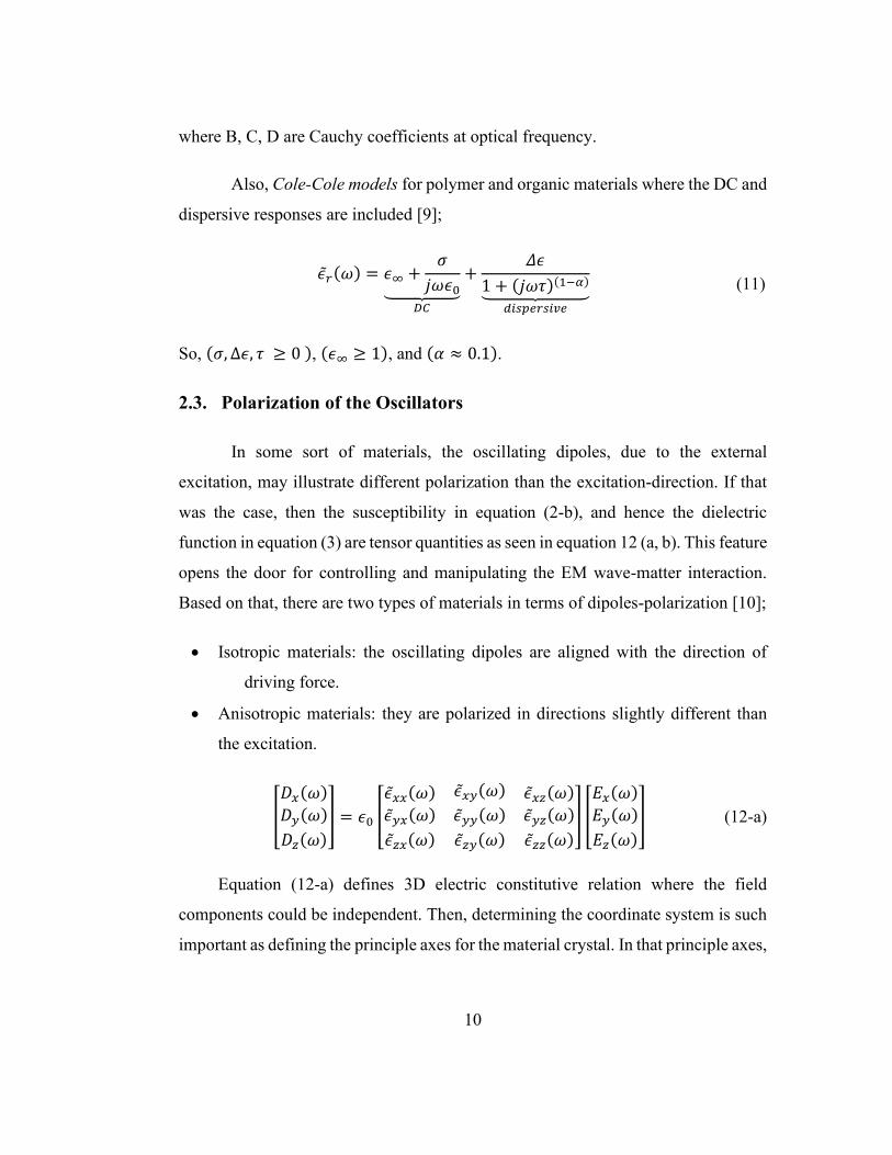
2.3. Polarization of the Oscillators
In some sort of materials, the oscillating dipoles, due to the external
excitation, may illustrate different polarization than the excitation-direction. If that
was the case, then the susceptibility in equation (2-b), and hence the dielectric
function in equation (3) are tensor quantities as seen in equation 12 (a, b). This feature
opens the door for controlling and manipulating the EM wave-matter interaction.
Based on that, there are two types of materials in terms of dipoles-polarization [10];
• Isotropic materials: the oscillating dipoles are aligned with the direction of
driving force.
• Anisotropic materials: they are polarized in directions slightly different than
the excitation.
[
𝐷𝑥(𝜔)
𝐷𝑦(𝜔)
𝐷𝑧(𝜔)
] = 𝜖0 [
𝜖�̃�𝑥(𝜔)
𝜖�̃�𝑥(𝜔)
𝜖�̃�𝑥(𝜔)
𝜖�̃�𝑦(𝜔)
𝜖�̃�𝑦(𝜔)
𝜖�̃�𝑦(𝜔)
𝜖�̃�𝑧(𝜔)
𝜖�̃�𝑧(𝜔)
𝜖�̃�𝑧(𝜔)
] [
𝐸𝑥(𝜔)
𝐸𝑦(𝜔)
𝐸𝑧(𝜔)
] (12-a)
Equation (12-a) defines 3D electric constitutive relation where the field
components could be independent. Then, determining the coordinate system is such
important as defining the principle axes for the material crystal. In that principle axes,

11
the unit vectors (�̂�, �̂�, �̂�) are not necessarily at 90o to each other, but they usually
match the coordinate system as shown in equation (12-b).
[𝜖�̃�𝑥(𝜔)00
0𝜖�̃�𝑦(𝜔)
0
00
𝜖�̃�𝑧(𝜔)] = [
𝜖�̃�(𝜔)00
0𝜖�̃�(𝜔)0
00
𝜖�̃�(𝜔)] (12-b)
Then, only the diagonal components in equation (12-a) represent the normal
alignment of an anisotropic material with the Cartesian system. The other
components in equation (12-a) represent the rotation of a material with respect to
these principle axes. In addition, equation (12-b) defines the three sorts of anisotropy:
1. 3D isotropic: [𝜖�̃� = 𝜖�̃� = 𝜖�̃�], such as a cubic crystal.
2. Uniaxial anisotropic: [𝜖�̃� = 𝜖�̃� ≠ 𝜖�̃�] where the similar called ordinary
(𝜖�̃� , 𝜖�̃�) = 𝜖�̃�, and the unique is extraordinary (𝜖�̃�) = 𝜖�̃�. Hexagonal and
Tetragonal crystals are such media.
3. Biaxial anisotropic: [𝜖�̃� ≠ 𝜖�̃� ≠ 𝜖�̃�], such as a monoclinic crystal.
2.4. Wave Vector Principles
According to the solid background owning from the previous sections, the
overall EM waves-matter interaction should be summarized in one vector quantity.
This quantity is the wave momentum or the wave vector (�⃗� ) as commonly known.
The magnitude and the direction of (�⃗� ) reveal how and where-to the resultant wave-
harmonic is interacting and propagating [10].
|�⃗� | =2𝜋
𝜆=2𝜋(𝑛)
𝜆0 (13)
�⃗� = 𝑘𝑎�̂� + 𝑘𝑏�̂� + 𝑘𝑐 �̂� (14)
The magnitude, equation (13), regards to the refractive index (n) of the
material while the direction, equation (14), describes the perpendicular direction of

12
the propagating waves. Also, the pure real quantity of �⃗� represents propagating wave
while the pure imaginary is the evanescent. Moreover, the higher values of wave
vector can define the 3D topology of the interested material and/or the overall
propagating medium. As seen in the past section, there are three types of the hosted
media; isotropic where all directions have equal phase momenta, uniaxial that have
only two equal phase momenta, and the biaxial where all directions are different to
each other.
Figure 2. Left to right: isotropic, uniaxial (�̃�𝐎 > �̃�𝐄), and uniaxial (�̃�𝐎 < �̃�𝐄) topology of
crystals. Also, color-bar shows the normalized optical axis (OA).
Figure 2 illustrates the topology of the isotropic and uniaxial media. Since
(�⃗� ), the red arrows, defines the direction and phase of propagation, then the regarding
velocity is the phase velocity (𝑣𝑝). But the poynting vector (𝑆 ) which is always
normal to the media-topology surface is the direction of the real propagating power.
Then, (𝑆 ), the blue arrows, defines the group velocity. In fact, the difference between
(�⃗� ) and (𝑆 ) directions is clearly noticed in the uniaxial crystals which provides unique
functionalities. Further, this uniaxial anisotropy feature will present better
functionalities when it is extreme [11]. Specifically, a hyperbolic response is noticed
with an extremely anisotropy media as shown in Figure 3.

13
Figure 3. Topology for Type-I (left) and Type-II (right) hyperbolic media.
Likewise the previous figure, the poynting vector, in Figure 3, denotes to the
group velocity (𝑣𝑔 =𝜕𝜔
𝜕�⃗� ) and perpendicular to the media surface and/or (�⃗� × �⃗⃗� )
plane [11]. The type-I and type-II hyperbolic features usually named as axial- and
tangential-planes, respectively. The axial term is referring to the wave vector aligned
with the optical axis (OA) of the crystal (�⃗� 𝑐), which usually is (�̂�) or (�̂�) direction,
and the tangential describes the surface wave vector (�⃗� 𝑡). As conclusion, extreme
uniaxial anisotropy feature (hyperbolic) is not only due to the condition (𝜖�̃� ≠ 𝜖�̃�),
but because these components have opposite signs.
2.5. Polaritons and Hosted Materials
The past section outlined the basic principles that defined the wave vector as
the best term for representing the interaction between a material and applied
excitation. This interaction introduces collective hybrid quasiparticles well-known
as POLARITONS differ based on the hosted material. Although there are several
type of polaritons such as cooper pairs in superconductors (Cuprate, FeSe, RuCl),
excitons in semiconductors (MoS2,WSe2), and magnon polaritons (Cr2, Ge2, Te6)
which also known as spin resonances in anti-ferromagnets [12], yet, this section

14
highlights different types of these quasiparticles considered as the most popular
which are; plasmon polaritons (PPs), and phonon polaritons (PhPs).
2.5.1. Metals
The underlying physics behind this sort of media depends strongly on the
frequency. Therefore, the verity of response in wide band spectrum starts with
microwave frequencies. In this low frequencies band, the metals in general are
perfect ~ good conductor, and there is no need for approximation or model, so a fixed
value for conductivity is adequate [6]. Next regime extends to near-infrared and
visible light where the conductivity will decrease and the models like Drude-Model
is considered. The third spectrum is the ultraviolet where the dielectric feature is
more obvious. Also in this high spectrum, exotic characteristics are noticed such as
ultraviolet transparency for Alkali metals, and strong absorption in transition-band
for noble metals [6].
PPs, class of polaritons, are referring to the metals like Ag, Au, Cu, Pt, Li or
metal alloys like; TiN, or even some doped semiconductors supporting excitons
could be considered as plasmonics with low losses like; n-CdO, n-InGaAs, In:ZnO
(=IZO), Ga:ZnO (=GZO), Al:ZnO (=AZO) [7]. In Figure 4, measured characteristics
for gold through different IR bands are shown. These data have been adopted
throughout our related studies as will be seen in the further sections.

15
Figure 4. Complex Dielectric Function for Gold (Au) through Infrared (IR) Spectrum-bands.
It should be mentioned that usage Au in many studies and applications is
attributing to its advantages like; matching to Drude-model behavior especially in IR
regime, stability under ambient conditions, and its compatibility to the biosensing
applications especially in medicine and biology [13].
2.5.2. Polar Dielectric Materials
This sort represents almost the third of 32 crystal classes of dielectric
materials. Their unique property is referred to the asymmetrical construction where
ionic and electronic forces are induced without any applied excitation, and
spontaneous polarization creates permanent dipoles [14]. Also, polar dielectrics
support the phonon polaritons such as; 4H-SiC, 3C-SiC, w-AIN, Al2O3, w-GaN,
ZnO, GaP, AlAs, InP, GaAs, InAs, BaF2, and InSb [7]. The complex dielectric
function of silicon dioxide (SiO2), compatible with Lorentz-model in equation (8-a),
is shown in Figure 5.

16
Figure 5. Dielectric function of the real system of [Si–O–Si] stretching vibration oscillator.
The parameters for the adopted Lorentz-model in Figure 5 are corresponding
to the real oxide data cited in [3]; dielectric background 𝜖∞ = 2.14, natural frequency
of phonons 𝜔𝑇𝑂 = 1064 cm−1, phono damping 𝛤 = 10 cm−1, and oscillator
strength 𝛺 = 950 cm−1. The unit (cm−1) is known for the wavenumber (𝑊#) which
is common for defining the frequency in spectroscopy and most chemistry fields
[15]. In fact, it has dimension of reciprocal wavelength (𝜆) in CGS unit-system, i.e.
reciprocal centimeters. So; 𝑊# =𝐹
(𝐶∗100).
2.5.3. Van der Waals Materials
In terms of crystalline structure, there are group of materials known as
Layered materials have strong extended crystalline planar by in-plane covalent
bonds, and weak out-of-plane due to Van der Waals (VdW) forces [16]. VdW-forces
are very weak, short-range, distance-dependent, and electrostatic attractive forces
arising from the permanent or transient interaction of dipole momenta [17].

17
Therefore, VdW materials are attributing to these weak bounded which forms
enhanced quantum effect materials as a resultant of reduction of available phase
space and diminished screening. Examples of these 2D materials extend to include
metals, polar insulator (dielectric), and even semiconductors and superconductor. So
that includes ‘‘graphene and its analogues, such as hexagonal boron nitride; black
phosphorus (BP) and its analogues; the III–VI family of semiconductors; and the
transition-metal dichalcogenides (TMDs)’’ [16]. In this section, the dielectric
function of graphene and hexagonal boron nitride (hBN) will be detailed.
2.5.3.1. Graphene
It was a result of innovative work that gained Physics Nobel Prize in 2010
[18]. This VdW material consists of hexagonal monolayer of carbon-atoms that has
unique response in Long- to Mid-IR spectrum.
Figure 6. Complex permittivity for graphene in many fermi-levels, equation (16).

18
Although graphene supports plasmons, however, it does not obey Drude-
model like Au. Therefore, Kobo Formula for complex conductivity-representation is
the common expression for graphene in many related literatures [19][20][21][22].
Exhibited results, in Figure 6, are plotted according to the following equations that
extracted from mentioned literatures.
𝜎 = (1
𝑍𝑆) = 𝜎intra + 𝜎inter (15-a)
𝜎intra = 𝑗𝑞2𝐾𝐵𝑇
2𝜋ℏ(𝑓 + 𝑗𝛤)[𝐸𝑓
𝐾𝐵𝑇+ 2 ∗ 𝑙𝑛 (𝑒
(−𝐸𝑓𝐾𝐵𝑇
)+ 1)] (15-b)
𝜎inter = 𝑗𝑞2
4𝜋ℏ𝑙𝑛 [2|𝐸𝑓| − 2𝜋ℏ(𝑓 − 𝑗𝛤)
2|𝐸𝑓| + 2𝜋ℏ(𝑓 − 𝑗𝛤)] (15-c)
where q is the electron charge (1.60217662×10⁻¹⁹ C), ℏ the reduced Plank constant
(1.0545718×10⁻³⁴ J.s/rad), 𝐾𝐵is the Boltzmann constant (1.38064852×10⁻²³ J/K), T
is room temperature (300 K), and 𝛤 is the damping rate. In addition, 𝐸𝑓 is the Fermi
level and also known as chemical potential of the graphene layer and it is defined in
Figure 6, for three levels: (0 eV), (0.25 eV), and (1 eV). Therefore, 𝐸𝑓 represents the
tuning knob for the graphene based on an applied bias voltage gate. For modeling
purpose, the complex permittivity for graphene is expressed in terms of the
conductivity (𝜎), free space wavelength (𝜆0), thickness of monolayer (d = 0.33 nm),
and free space wave impedance (𝜂0 = 377𝛺).
𝜖𝑟 = 1 + 𝑗𝜆0𝜂0𝜎
2𝜋𝑑 (16)
2.5.3.2. Hexagonal Boron Nitride (hBN)
Like a graphene, hBN belongs to VdW materials with naturally hyperbolic
dispersive properties in the mid-infrared spectrum. Specifically (22.8 THz ~ 24.75

19
THz) for the lower reststrahlen band, and (40.79 THz ~ 48.42 THz) for the upper
reststrahlen band [11]. It should be mentioned that these lower- and higher-limits for
reststrahlen bands represent transverse optical (TO) and longitudinal optical (LO)
resonances. However, hBN is a polar insulator (or dielectric) and each complex
permittivity for these two reststrahlen bands is described in equation (8-a) by Lorentz
oscillator [23][24]. It should be noticed that the lower reststrahlen band usually
named as type-I while the upper reststrahlen band is called type-II as explained in
section (2.4). Figure 7 illustrates the topology for type-I and II beside the optical
properties for hBN.
Figure 7. Complex dielectric function for hBN with yellow-highlighting for its lower and
upper reststrahlen-bands, type-I and II respectively, according to data in [11].

20
Chapter 3: Computational Methods for Analysis
Although the field of nano-optics, or nanophotonics, is a hundred years old
[6], yet the rapid development in computing power and speed beside nanofabrication
has made this field promising recently. Therefore, powerful numerical/computational
techniques represent an important class of modern researches in nanophotonics. The
relevant techniques/methods are classified based on the prospect of the aimed
structure/design.
Figure 8. Numerical methods chart: the red-identified are the relevant to this dissertation.
Figure 8 summarizes a group of NMs in three main categories in terms of the
design-expectations. The listed abbreviations in Figure 8 are examples for these
categories; FEM = Finite Element Method, FDTD = Finite Difference Time Domain,
MoM = Method of Moments, RCWA = Rigors Coupled Wave Analysis, MoL =

21
Method of Lines, BPM = Beam Propagation Method, TMM = Transverse Matrix
Method, RT = Ray Tracing, GTD = Geometrical Theory of Diffraction, and PTD =
Physical Theory of Diffraction. Only the methods highlighted with red color will be
considered in this dissertation as will be seen accordingly.
3.1 FEM Principles
Although this method was originally devoted to solve structural analysis
problems in civil and aeronautical engineering, however, the flexibility and
versatility features of FEM have attracted several disciplines recently [25].
Electromagnetics is one of these appropriate areas that adopted FEM as powerful
technique in low frequency, scale size-based analysis [26]. Since FEM introduces
good approximation for inhomogeneous media, curvatures and circular structures by
discretizing the continuous computational domain, FEM mesh can be used in key
regions without facing convergence issue [27]. Usually FEM mesh is a built-in
feature in a commercial FEM simulator-software. The used simulator in this study is
unified user interface called ANSYS Electronics Desktop 2019, or HFSS as
commonly known. So, the modelling process starts by building up the interested
model in HFSS-environment, and defining the properties of relevant materials,
appropriate boundary conditions and excitation. Next to that will be meshing process
where ‘‘the physics defines the mesh rather than the mesh defining the physics’’ [28].
Namely, HFSS has an automatic tool for meshing process beside another tool for
user-option called mesh operation. So, the meshing process will continue
automatically till convergence condition is met, or till the number of adaptive passes
is passed. Details and needed support are provided by help-tool in the user interface
in very clear searchable way.

22
Figure 9. Meshing in HFSS environment.
As shown in Figure 9, the objects-discretization is in form of connected
elements where there are a linear, or a surficial, or a volumetric element. Each
element has number of nodes; two for linear, and three for surficial, and four
(tetrahedron) for volumetric element according to the default setting of HFSS solver.
From mathematical prospective, the computational domain that FEM, or its
simulator, will discretize into several elements is described by Maxwell-equations.
Therefore, HFSS mathematically solves Maxwell-equations under certain conditions
at those nodes and set of eigenvalue problems will be formed based on those
elements. Regardless of the model-conditions (Driven or Eigen as available in the
simulator), HFSS has capability to categorize an electromagnetic structure in a
compact manner using the concept of S-parameters. This categorization is in terms
of the incident and reflected/transmitted modal amplitudes, so HFSS provides S-
matrix automatically for Driven-modal (with ports). In case of Eigen-modal (with
no port), S-matrix is computed based on circuit theory using Modes-to-Terminals
23
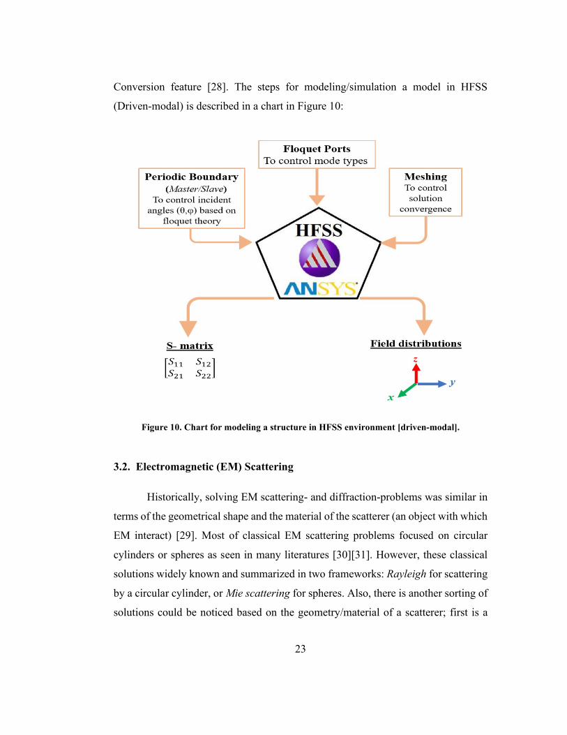
Conversion feature [28]. The steps for modeling/simulation a model in HFSS
(Driven-modal) is described in a chart in Figure 10:
Figure 10. Chart for modeling a structure in HFSS environment [driven-modal].
3.2. Electromagnetic (EM) Scattering
Historically, solving EM scattering- and diffraction-problems was similar in
terms of the geometrical shape and the material of the scatterer (an object with which
EM interact) [29]. Most of classical EM scattering problems focused on circular
cylinders or spheres as seen in many literatures [30][31]. However, these classical
solutions widely known and summarized in two frameworks: Rayleigh for scattering
by a circular cylinder, or Mie scattering for spheres. Also, there is another sorting of
solutions could be noticed based on the geometry/material of a scatterer; first is a

24
compact or closed-form solution for certain/defined shape, second is an integral-form
solution for an arbitrary shape. Later, after all those efforts, simple and compact
formulations had been presented in many literatures for solving EM scattering
problems in different computational domain [29]. The key for all solutions is the
wave vector where the incident, scattered, and internal fields are addressed in series
expansions/harmonics of the wave vector as analytical solving of Maxwell equations.
The term cross section facilitates solving EM scattering by dealing with
scattered, absorbed, extinction power in form of area carried by the source/incident
EM wave (𝐴𝑆).
𝑆𝐶𝑆 =∯𝑃𝑠𝑐𝑡�̂� 𝑑𝑠⃗⃗⃗⃗ =
12∯𝑅𝑒[𝐸𝑠𝑐𝑡 × 𝐻𝑠𝑐𝑡
∗ ] �̂�𝑑𝑠⃗⃗⃗⃗
(𝑃𝑖𝑛𝐴𝑆)
=𝑊𝑠𝑐𝑡 [ Watt ]
(𝑃𝑖𝑛𝐴𝑆) [Watt / m2]
(17)
𝐴𝐶𝑆 =
12∭ 𝑅𝑒[(𝜎𝐸 + 𝑗𝜔𝐷)𝐸∗ = 𝑗𝜔𝐵𝐻∗] 𝑑𝑣
𝑉
(𝑃𝑖𝑛𝐴𝑆)
=𝑊𝑎𝑏𝑠 [ Watt ]
(𝑃𝑖𝑛𝐴𝑆) [Watt / m2]
(18)
𝐸𝐶𝑆 = 𝑆𝐶𝑆 + 𝐴𝐶𝑆 (19)
Equations (17), (18), (19) define scattered, absorbed, and extinction cross
sections respectively where SCS is derived by integrating the poynting vector over
the scatterer while ACS is derived by integrating the energy loss over the volume of
the object. Therefore, this form of solution is considered as integral-form that fits
any complex arbitrary shape in computational domain. The common methods for
implementing such solution, especially in nano-matter scale, are full wave-
techniques [3][32]. Here FEM is chosen for this purpose where HFSS-solver
provides the poynting vector and volumetric energy loss calculations as built-in
functions (Poynting, and VolumeLossDensity) in the field calculator tool.

25
3.3. Effective Medium Theory
The aim of this method is introducing a homogeneous effective medium
based on the spatial wave vector-distribution. The discontinuities, or interfaces,
between different media define a new momentum called grating vector (�⃗⃗� 𝑔) plays a
crucial rule. So, there is a correlation between the polarization of incident field (�⃗� )
and �⃗⃗� 𝑔that represents the arrangement of the interfaces.
(a). 𝝐𝒆𝒇𝒇𝒆𝒄𝒕𝒊𝒗𝒆 = 𝝐∥ (b). 𝝐𝒆𝒇𝒇𝒆𝒄𝒕𝒊𝒗𝒆 = 𝝐⊥ (c). 2D effective Medium.
Figure 11. Scenarios of Effective Medium Theory (EMT).
As shown in Figure 11(a) and 11(b) respectively, there are two scenarios for
�⃗� polarization; either parallel to the interfaces and perpendicular to �⃗⃗� 𝑔, or vices
versa. That means there are two possible conventions for defining the effective
media, yet the adopted convention here is defining �⃗� polarization with respect to the
interfaces not �⃗⃗� 𝑔. Hence, Figure 11(a) is the parallel effective medium while Figure
11(b) represents the perpendicular effective medium. Analyzing the boundary
conditions explains the differences where;

26
• In the parallel scenario, Figure 11(a), �⃗� is tangential to the interfaces and
continuous across the interfaces. In contrast, the field density (�⃗⃗� = 𝜖 �⃗� ) is
discontinuous, so (�⃗⃗� 𝐻 = 𝜖𝐻 �⃗� 𝑎𝑣𝑒) and (�⃗⃗� 𝐿 = 𝜖𝐿 �⃗� 𝑎𝑣𝑒) where 𝜖𝐻 and ϵ𝐿 are the
higher and lower dielectric properties and �⃗� 𝑎𝑣𝑒 is the average field intensity while
(ff) is filling factor that addresses the relation between thicknesses [𝑓𝑓 =
(𝑤𝑖𝑑𝑡ℎ𝐻)
(𝑤𝑖𝑑𝑡ℎ𝐻+𝑤𝑖𝑑𝑡ℎ𝐿)]. Then:
�⃗⃗� 𝑎𝑣𝑒 = 𝑓𝑓�⃗⃗� 𝐻 + (1 − 𝑓𝑓)�⃗⃗� 𝐿 = 𝑓𝑓𝜖𝐻�⃗� 𝑎𝑣𝑒 + (1 − 𝑓𝑓)𝜖𝐿�⃗� 𝑎𝑣𝑒
∴ 𝜖𝑒𝑓𝑓(∥) =�⃗⃗� 𝑎𝑣𝑒
�⃗� 𝑎𝑣𝑒= 𝑓𝑓𝜖𝐻 + (1 − 𝑓𝑓)𝜖𝐿 (20)
• The second scenario when �⃗� is perpendicular to interfaces, as seen in Figure
11(b), where �⃗⃗� is continuous across the interfaces instead of �⃗� . As a result, (�⃗� 𝐻 =
𝜖𝐻−1 �⃗⃗� 𝑎𝑣𝑒) and (�⃗� 𝐿 = 𝜖𝐿
−1 �⃗⃗� 𝑎𝑣𝑒), also;
�⃗� 𝑎𝑣𝑒 = 𝑓𝑓�⃗� 𝐻 + (1 − 𝑓𝑓)�⃗� 𝐿 = 𝑓𝑓(𝜖𝐻−1)�⃗⃗� 𝑎𝑣𝑒 + (1 − 𝑓𝑓)(𝜖𝐿
−1)�⃗⃗� 𝑎𝑣𝑒
∴ 𝜖𝑒𝑓𝑓(⊥) =�⃗⃗� 𝑎𝑣𝑒
�⃗� 𝑎𝑣𝑒=
1
𝑓𝑓𝜖𝐻−1 + (1 − 𝑓𝑓)𝜖𝐿
−1 (21-a)
or 𝜖𝑒𝑓𝑓(⊥) =𝜖𝐻 𝜖𝐿
𝑓𝑓𝜖𝐿 + (1 − 𝑓𝑓)𝜖𝐻 (21-b)
• Unlike the previous two cases where the layers-stack assumed to have 1D
variation, Figure 11(c) is regarding to 2D effective medium calculations, so an
isotropic distribution of a certain geometry, here cylindrical nanorods along Z-
axis, is considered. Therefore, applying generalized Maxwell–Garnett (MG)
method defines the permittivity components (⊥ & ∥) [33].
𝜖𝑒𝑓𝑓(∥)(𝑀𝐺) = 𝑓𝑓𝜖𝐻 + (1 − 𝑓𝑓)𝜖𝐿 (22)
𝜖𝑒𝑓𝑓(⊥)(𝑀𝐺) =(1 − 𝑓𝑓)𝜖𝐿𝜖𝐻 + (1 − 𝑓𝑓)(𝜖𝐻)
2
(1 − 𝑓𝑓)𝜖𝐻 + (1 + 𝑓𝑓)𝜖𝐿 (23)
• For higher order-harmonics due to subwavelength greetings (1D or 2D, a study
addressed in [34] had presented up to 4th order for TE (⊥ here), and up to 2nd

27
order for TM: (∥ here). Although the (⊥) effective permittivity is explicit, yet the
(∥) effective permittivity is complex due to including Fourier coefficients (𝑎𝑛)
[34];
𝜖⊥ = 𝜖𝑎𝑣𝑒 +(𝛥𝜖𝑟)
2
2(𝛥
𝜆)2
+ 2𝛽2(𝛥𝜖𝑟)2 (𝛥
𝜆)4
(24)
where 𝜖𝑎𝑣𝑒 =(𝜖𝐻+𝜖𝐿)
2, Δϵ = (𝜖𝐻 − 𝜖𝐿), and 𝛽 = 𝑛𝑖𝑛𝑐 𝑠𝑖𝑛 𝜃𝑖𝑛𝑐.
𝜖∥
= 1
𝜖0𝑎0
[
𝜖0 − 𝛽2 + 𝜖0𝑎0𝛽
2
+ (𝛥
𝜆)2
{
𝛽4(𝛥𝜖)2
2𝜖02 +
𝛽2(𝛥𝜖) (1 −𝛽2
𝜖0)(2𝑎1𝑎0
+(𝛥𝜖)𝑎22𝜖0𝑎0
) +
𝜖0
𝑎02 (1 +
𝛽4
𝜖02 −
2𝛽2
𝜖0) [𝜖0∑(
𝑎𝑛𝑛)2
𝑛≠0
+ 2(𝛥𝜖)∑𝑎𝑛(𝑎𝑛+1)
𝑛(𝑛 + 1)𝑛>0
]}
]
(25)
3.4. Transfer Matrix Method (TMM)
This method solves Maxwell equations for the field that propagating
throughout 1D multilayers structure as seen in Figure 12. So, mathematical
expressions relate the field from one layer to the other are formed in a matrix [35].
Likewise the analysis of the fields at interfaces in the past section, the normal field
densities (�⃗⃗� 𝑛 and �⃗� 𝑛) and tangential field intensities (�⃗� 𝑡 and �⃗⃗� 𝑡 ≡ 𝛹𝑡) are passing
to the next layer regardless of medium properties ([𝜖] and [𝜇]) or medium thickness
(d).

28
Figure 12. A physical description of applying TMM for 1D structure.
Therefore, TMM is simple, accurate, and robust for several theoretical studies
like determining the reflection and transmission spectra [36][37], band diagram
calculations [38], and guided modes [39]. The process steps for this technique using
Matlab-environoment are summarized in the chart in Figure 13.
As detailed in Figure 13 and summarized in Figure 12, the overall fields-equation in
matrices form could be calculated;
[𝛹𝑡(𝑡𝑟𝑎𝑛𝑠𝑚𝑖𝑡𝑡𝑒𝑑 − 𝑠𝑖𝑑𝑒)]𝑚×1 = [𝑇𝑟(𝑔𝑙𝑜𝑏𝑎𝑙)]𝑚×𝑚[𝛹𝑡(𝑖𝑛𝑐𝑖𝑑𝑒𝑛𝑡 − 𝑠𝑖𝑑𝑒)]𝑚×1 (26)
where the global matrix represents the transfer matrix for overall structure as:
𝑇𝑟(𝑔𝑙𝑜𝑏𝑎𝑙) = (𝑇𝑟1)(𝑇𝑟2) ⋅⋅⋅ (𝑇𝑟𝑁) (27)

29
Figure 13. Chart for TMM process-steps using MatLab.

30
Chapter 4: Analysis and Designs
The common base between all nanophotonic-designs is engineering or
manipulating the EM-matter interactions. For sensing applications, maximize the
enhancement, coupling, hence the sensitivity, is the main purpose for engineering
light-matter interactions. In fact, different engineering methods have been headed
toward this goal including nanostructures geometries, arrangements, and materials.
Therefore, the sections in this chapter represent the contributions of this dissertation.
4.1. Coupling Between Metallic Structure and Phonon Polaritons for Sensing
Applications [40]
This work identifies the resulting coupled modes between metallic structure
and 2D phonon polaritons (PhPs) using finite element analysis backed up by cross
section areas method. The analysis of the integrated structure reveals the nature of
the generated quasi-particles and the anti-crossing behavior as a signature for
coupling. In fact, the first motivation was inferred from heterostructures consist of
plasmonic materials (like graphene) and anisotropic phononic materials (like hBN)
that offering coupled polariton modes (PP-PhP) [41]. In this heterostructure, the
graphene exhibits a tunable and wider response, and hBN is confining the light in
different volumetric shapes to provide large field enhancements. Also, exploring
PhPs in hBN antenna / waveguide was carried out experimentally and theoretically
for the first time where surprising modes were discovered [42].
These works were encouraging and attracting us to investigate the dispersive
PhPs in hBN antenna / waveguide as seen in Figure 14. The geometry of hBN
antenna was defined, in HFSS simulator, according to the Figure 14(a) with several
widths as listed in Figure 14(c). By applying incident plane wave that has orthogonal

31
polarization of (E-field) with hBN-antenna axis and operating band (37 THz ~ 50
THz), type-II properties of hBN are the dominant where Lorentz oscillator model
represents this properties and the longitudinal optical frequency (LO), lower
interface [SiO2] surface phonon frequency (LI), and upper interface [air] surface
phonon frequency (UI) are determined via energy loss function (ELF). In contrast
with the higher losses offered by natural/transversal optical frequency (TO), ELF
reveals the resonances corresponding to lowest losses at the lower, upper interfaces
and the bulk materials. Mathematically, ELF is the negative opposite of the
imaginary part of a dielectric function [3];
𝐸𝐿𝐹 = 𝑖𝑚𝑎𝑔 (−1
𝜖𝐿𝑜𝑟𝑒𝑛𝑡𝑧) (28-a)
𝐸𝐿𝐹𝑑 = 𝑖𝑚𝑎𝑔 (−1
(𝜖𝐿𝑜𝑟𝑒𝑛𝑡𝑧 + 𝜖𝑑)) (28-b)
where 𝜖𝐿𝑜𝑟𝑒𝑛𝑡𝑧 is the corresponding type-II hBN oscillator while 𝜖𝑑 surrounding
medium (upper = air, or lower = SiO2). Hence, 𝐸𝐿𝐹related to a pure hBN while 𝐸𝐿𝐹𝑑
represents the upper interface [air/hBN] or the lower interface [hBN/SiO2].
At HFSS simulator, the available simulation-modes for nonplanar sources
are: scattered, total, and incident-filed mode. So SCS and ACS are obtained using
scattered- and total-modes, respectively, while ECS = SCS + ACS. Figure 14(c)
depicts the results for ECS at different widths where wider hBN-antenna provides
stronger ECS. Peaks for each width in Figure 14(c) represents the dispersion curves
in Figure 14(d) where 𝑘 =𝜋
(𝑊ℎ𝐵𝑁). Further, the enhancement [𝐸𝑚𝑎𝑥
2 =
𝑚𝑎𝑥(𝐸𝑣𝑜𝑙𝑢𝑚𝑒 ⋅ 𝐸𝑣𝑜𝑙𝑢𝑚𝑒∗ )] has results for each width, so the peaks for each width are
presented in Figure 14(d) as purple curve along with the dispersion curves. As results,
the match between the dispersion and enhancement could be noticed for wider hBN-
antennas at longer wavelengths.

32
Figure 14. (a). hBN antenna placed on SiO2 substrate. (b). Complex (𝛜𝒉𝐁𝐍−𝐈𝐈) and ELF. (c).
Extinction cross section areas (ECS) for different widths (W) according to the model in (a) and
equation (19). (d). Dispersion curves based on the peaks of ECS in (c). The inset in (d)
explained the corresponding peaks with an example ECS (W=200 nm).
In addition, the second motivation was introduced by the study cited in [3]
where strong coupling between plasmons (PPs), caused by Au, and surface phonon
polaritons (SPhPs), caused by SiO2, was proved. Therefore, this motivating study

33
and other similar works [43][44][45], have confirmed that the strong coupling in IR
regime can be achieved by placing metallic structures on the top of ionic films.
Moreover, these ionic films-studies showed that there is an induced transparency
window caused by strong coupling between PPs and SPhPs.
Based on that, a new structure includes Au-rod beside hBN-antenna placed
together above SiO2 substrate as shown in Figure 15(a), then a graphene monolayer
is injected between [Au+hBN] rods and SiO2 substrate as seen in Figure 15(b).
According to the features of the used materials, and the capacitive excitation for
SPhPs, as a result of the gap between the rods, the design leverages high
enhancement and strong coupling between PPs and SPhPs in mid-IR regime [40].
Figure 15. The designed structure; (a) without, (b) with graphene monolayer.
It should be mentioned that the designed structure is modeled in HFSS
simulator where the length (L) in Figure 15 has eight values defined in (𝜇𝑚) as;
1.2566, 1.5708, 1.75, 1.9, 2.0944, 2.25, 2.5, and 3.1416. These lengths are swept for
two widths (W); [50 nm, 200 nm] while the width of the air-gap is fixed (t = 25 nm),
and the substrate has permittivity 𝜖𝑆𝑖𝑂2 = 2.25, and large dimensions in (X, Y, Z) to

34
avoid any outer interferences across the radiation boundaries in HFSS-environment.
In addition, the applied source is plane wave placed at the upper face of the model-
cell with E-field parallel to X-direction.
Figure 16. Results for (W= 50 nm) of hBN antenna; (a ~ h) SCS (red), ACS (blue), and ECS
(black) for the system. The dispersion relation is plotted in (i) according to the positions of the
largest peaks of ECS curves in (a-h). Those peaks represent the dominant modes per each
length (L) exactly as marked with the red circles. The three vertical dashed lines are TO, UI,
and LO for (a ~ h) from left to right, and from bottom to top for plot (i).

35
Figure 17. Results for hBN antenna with width (W = 200 nm); like a previous figure, (a ~ h)
are cross section areas for different length while (i) the corresponding dispersion relation.
Likewise the results in Figure 14(c) and (d), the three cross section areas,
SCS, ACS, and ECS for the model in Figure 15(a) are computed at (W = 50 nm) in
Figure 16, and at (W = 200 nm) in Figure 17. From the parts (a ~ h) in both Figure
16 and (17), gradual coupling between the dark modes (sharp peaks) and the bright
modes (wide peaks) is clearly seen. Moreover, inside the reststrahlen band, which is
defined by the outer vertical green dashed lines in the regarding results, the wider
hBN-antenna (W = 200 nm) offered more dark modes comparing with (W = 50 nm).
36
In terms of cross section areas, SCS curves are larger than ACS in both
Figure 16 and (17) which indicates a dominant behavior known as electromagnetic
induced transparency (EIT) instead of its counterpart; electromagnetic induced
absorption (EIA) [13]. Based on that, these results reflect the scenario of
overcoupling (OC) that has external losses exceed the internal/absorption losses.
By applying the same procedure for determining the cross section areas and
the dispersions on the model in Figure 15(b), the influence of graphene layer is
noticeable as shown in Figure 18 and (19) for (W = 50, 200 nm) respectively. The
ability of tuning the Femi-level of the graphene, plays the major role in tuning the
dispersion relations where these relations are classified into two group; dispersion
results for the dominant modes (connected dots with solid curves), and dispersion
results for the enhanced modes (dots connected by dashed curves). The dominant
modes represent the peaks of ECS while the second group are extracted from the
resonances that corresponding to the largest peaks of field-enhancement results
(𝐸𝑚𝑎𝑥2 ).
Briefly, the influence of the increased Fermi-level is interpreted with two
widths of the model as a blue-shift, shift in frequency toward the highest, of the
coupling characteristics. This shift for the dominant modes (solid curves) is
accompanied with a relative decreasing of the gap in the dispersion relation. In fact,
this gap due to the separation between two branches of a dispersion curve is known
as gap-spacing, and the quantum theory defining the coupling as an anti-crossing
(splitting) of the dispersion relation [46][47].

37
Figure 18. (a). Dispersion relations for model with (W=50 nm) has different graphene levels
(No graphene= black, 0 e.V= blue, 0.25 e.V= red, and 1 e.V= green). (b ~ d). Respectively,
ECS, ACS, and field enhancement for model with length (L = 2.0944 𝛍𝐦).
Figure 19. Like the previous figure: these results for the model with W = 200 nm.

38
In other words, the gap-spacing became fully controlled by Fermi-level (or
known as chemical potential) of the graphene, and the reciprocal amount of this gap
determining coupling strength [48]. Parts (b ~ c) in both Figure 18 and (19) illustrate
losses decreasing as the graphene level is increased. Further, the enhancement results
for (W = 50 nm) depicts the highest enhancement as 6 order of magnitude (5 × 10⁶)
corresponding to 45.4 THz which is the 4th ord6er mode. Likewise, the model with
width = 200 nm offers the largest enhancement (1.75 × 10⁶) that corresponding to
the 4th order mode as well at 44.3 THz.
The field enhancement depends on the width of hBN antenna and the
enhanced wavelength where thinner hBN-antenna means there will be higher wave
vector (K) (or effective refractive index) which can squeeze more waves into a small
volume. Mathematically, the difference between the wave vector for two width cases
is described based on the reststrahlen band limits (TO, and LO) of type-II hBN as
following:
𝑘50𝑛𝑚 =𝜋
50𝑛𝑚= 62.83 × 10⁶ ⇒ 123.2 ≤ (
𝑘50𝑛𝑚𝑘0
) ≤ 146.12 (29)
𝑘200𝑛𝑚 =𝜋
200𝑛𝑚= 15.71 × 10⁶ ⇒ 30.8 ≤ (
𝑘200𝑛𝑚𝑘0
) ≤ 36.53 (30)
4.2. Hybrid FEM/TMM Technique and Dispersive hBN (Type_II) [49]
4.2.1. Introduction
FEM and TMM are two common numerical mature methods have been
explained in the past chapter. Therefore, leveraging the accuracy and the simplicity
from the combination of these two methods offering a novel technique determining
the dispersion relations for a hetero-structure. Especially in nano-scale, modeling the
geometry of interest using a FEM simulator (HFSS) and modifying the outputs to
match a simpler technique (TMM) for extracting the dispersion is the brief

39
description of the hybrid technique as charted in Figure 20(a). According to this
chart, the benefits of both FEM and TMM are captured, and the whole modifications
are related to S-matrix data.
Figure 20. (a) Chart for Hybrid FEM / TMM technique. (b) hBN (Type-II) model in HFSS. (c)
S-matrix representation for (TE=mode#1) and (TM=mode#2) of Floquet Ports [FP#].
Namely, S-matrix interprets the interaction between EM (incident, reflected,
and transmitted) waves and the whole periodic structure in longitudinal directions.
The complex scenario is the case with multidirectional periodic structure such as the
hetero-structures that have stack of layers in Z-axis or surface gratings in (X, Y) axis.
In contrast, the simple scenario is the case with 1D longitudinal direction which is
exactly like TMM analysis. Using HFSS, the periodicity in any two directions is
modeled by Master/Slave boundaries while the third direction is place for Floquet-
Port sources.

40
4.2.2. Principle
The model in Figure 20(b) depicts an example for build a complex scenario;
a slab of hBN (Type_II) in HFSS-environment with periodicity in (Z, X) where
Master/Salve boundaries are placed. The Floquet sources are placed at the two
perpendicular faces to Y-axis. In this model/cell, the atomic stack of hBN-crystal is
layered in Z-axis, so the applied EM waves are perpendicular to the optical axis
(OA). This kind of excitation will trig the surface modes for hBN (Type-II). Also,
the whole cell will be replicated in (X, Z) directions to mimic the periodicity using
these kinds of boundaries and sources.
The practical analysis starts by extracting TMM from the S-matrix for the
entire model which has incident (i)- and transmitted (t) -terminals, and input- and
output-modes for each terminal. Therefore, S-matrix reflects the correlation between
input and output regardless of the terminals, equation (31), while TMM sorts the
modes for each terminal, equation (32). It should be mentioned that this S-matrix
reflects the interaction inside a 3D structure, so the corresponding TMM is referred
for each periodic direction.
[ℂ𝑖−
ℂ𝑡+] = [
𝕊𝑖𝑖 𝕊𝑖𝑡𝕊𝑡𝑖 𝕊𝑡𝑡
] [ℂ𝑖+
ℂ𝑡−] (31)
[𝕆𝕀
−𝕊𝑖𝑡−𝕊𝑡𝑡
] [ℂ𝑡+
ℂ𝑡−] = [
𝕊𝑖𝑖 −𝕀𝕊𝑡𝑖 𝕆
] [ℂ𝑖+
ℂ𝑖−] (32)
Also, it should be noticed that equation (32) is extracting directly from (31)
with simple algebra. For equations (31) and (32); [ℂ±] are vectors of mode
proportionality (amplitudes) as defined in section 3.4, the signs (±) define a
consistent direction of the mode propagation; (+) propagation = from (i) to (t) and (-
) propagation for the opposite direction, [𝕊] is the S-matrix components, [𝕀] is the
identity matrix, and [𝕆] is a zero matrix [50].

41
According to Bloch or Floquet theory as usually named [51], applying the periodic
condition, equation (33-a), and specifying the periodicity in this condition to the
unity (N=1), that limits the number of analyzing cells into one cell as seen in equation
(33-b).
[ℂ𝑡+
ℂ𝑡−] = 𝑒𝑥𝑝
𝑗(𝐾𝑑)∗𝑑𝐿∗𝑁 [ℂ𝑖+
ℂ𝑖−] (33-a)
[𝐶𝑡+
𝐶𝑡−] = 𝑒𝑥𝑝
𝑗(𝑅𝑒[𝐾𝑑]±𝐼𝑚[𝐾𝑑])∗𝑑𝐿 [𝐶𝑖+
𝐶𝑖−] (33-b)
[𝐶𝑡+
𝐶𝑡−] = [
𝑒𝑥𝑝𝑗(𝐾𝑑)∗𝑑𝐿 0
0 𝑒𝑥𝑝−𝑗(𝐾𝑑)∗𝑑𝐿] [𝐶𝑖+
𝐶𝑖−] (33-c)
Based on that, the periodic behavior in the whole (identical cells) structure is
representing by this single cell that has defining geometry. Further, by defining the
geometry’s dimension (dL) according to the periodic directions, a set of generalized
eigen-value problems, [𝐴𝑥 = 𝜆𝐵𝑥], is obtained as seen in equation (34).
[𝑆𝑖𝑖 −1𝑆𝑡𝑖 0
] [𝐶𝑖+
𝐶𝑖−] = [𝑒𝑥𝑝
𝑗(𝐾𝑑)∗𝑑𝐿]𝑑𝑖𝑎𝑔
[01
−𝑆𝑖𝑡−𝑆𝑡𝑡
] [𝐶𝑖+
𝐶𝑖−] (34)
Equation (34) is a resultant from applying equation 33(b-c) into (32), and it is solved
using MatLab function [𝑊, 𝐸𝑑] = 𝑒𝑖𝑔(𝐴, 𝐵) where [𝑊] is the eigen-vectors, [𝐸𝑑]
is the eigen-values, 𝐴 = [𝑆𝑖𝑖 −1 ; 𝑆𝑡𝑖 0], 𝐵 = [0 −𝑆𝑖𝑡 ; 1 −𝑆𝑡𝑡], and 𝑥 =
[𝐶𝑖+ 𝐶𝑖
−]𝑇. Since the eigen-values reflect the picture of mode’s propagation (phase
and losses), and eigen-vectors describe the picture of fields (amplitudes of modes),
then the complex wave vector (𝐾𝑑) in a periodic direction, [𝑑𝐿], can be extracted
from these modified eigen-values (𝜆𝑘) for harmonics-order (m=...-2,-1,0,1,2,...);

42
𝜆𝐾 = 𝑑𝑖𝑎𝑔 (𝑑𝑖𝑎𝑔(log(𝑑𝑖𝑎𝑔(𝐸𝑑)))) (35)
𝐾𝑑 = 𝛽 ± 𝛼 = (𝑖𝑚𝑎𝑔(𝜆𝐾) + (2𝜋 ∗ 𝑚)
𝑑𝐿) ± 𝑗 (
𝑟𝑒𝑎𝑙(𝜆𝐾)
𝑑𝐿) (36)
4.2.3. Benchmarking
As benchmarking for this hybrid technique, the results regarding to the model
in Figure 20(b) are presented in Figure 21(a-b) beside the experimental investigated
results Figure 21(c) for the same model [11]. Since the floquet port in HFSS-solver
is provided with built-in Mode Calculator, so the control for the fundamental TE and
TM modes is possible using this tool. In fact, most of the applied power is formed in
these incident, fundamental modes (TE00, TM00) as seen addressed in the related
technical report [52].
Figure 21. (a-b): Reflection (R), transmission (T) and absorption (A) for a slab of hBN (Type-
II) as modeled in Figure 20(b) for different incident-angle (𝛉𝟎 = 𝟏𝟎 ~ 𝟗𝟎) while (𝛟𝟎 = 𝟗𝟎),
and medium 1 and 2=Air. Also, L=W=1.618 𝛍𝐦. (c). Experimental results for the
corresponding material (flak of hBN upon BaF2 substrate) as cited in [11].

43
Therefore, comparing the modeled results with the corresponding
experimental shows identification with TE results only, however, the highest
absorption results are noticed for TM results. The physical interpretation for that is
regarding to the measurement’s way for the experimental results where the
measuring/probing tool was placed on or closed to the surface of hBN flake which is
known as imaging method to excite the modes based on phase matching-principle
[42][53]. In contrast, simulation method provides insight for the internal and external
generated modes. Therefore, the incident mode TM00 is the right mode to illustrate
the dispersion features due to the highest absorption index. Also, the phonon
polaritons are usually resultant for TM modes where magnetic field is orthogonal to
the optical axis (OA) [11]. Example of the simulated and non-imaging excitation for
hBN (Type_II) modes are shown in Figure 22.
Figure 22. Dispersive modes distribution for the model of hBN-slab shown in figure (20-b)
based on TM00 (left) and TE00 (right) excitation modes.
The most noticeable points from the Figure 22 are related to the illustrated
modes in both excitation where the both results (TM and TE) are considered as TE.
Due to the source orientation (𝜃, 𝜙), the results in Figure 22 are defined for TE plane
which is the same plane for experimental results in Figure 21(c).

44
Moreover, adopting TM00 excitation for the model sketched in Figure 20(b),
where the thickness (Tck) and the length (W=L) are changed, can show the relation
between absorption and the slab’s geometry for defining spectrum. All simulations
are achieved when (𝜃 = 60) due to the best momentum matching as seen in Figure
21(b).
Figure 23. Absorption Vs Frequency relationship for the model depicted in Figure 20(b) based
on TM00 excitation and (𝛉 = 𝟔𝟎,𝛟 = 𝟗𝟎).
The absorption results in Figure 23 reveal that the largest absorption for a
pure hBN-model (when medium 1, 2 are not exist) took place at (LO) resonance. In
contrast to (TO), (LO) resonance represents the less resistance which explains this
highest absorption. By introducing other media (medium 1 and 2 = Air) to
sandwiching the slab of hBN, this absorption will be decreased as the resonance will

45
be shifted away from (LO) simultaneously. In fact, all the presented resonances
except (LO) are surficial resonances dependence on the energy loss function (ELF)
as detailed in section (4.1) previously. Further, results in Figure 23 describe how the
absorption and the resonance are proportionally decreasing with the thickness of slab
hBN where medium (1, 2) get thicker at the same time. In addition, (length Vs.
absorption) relation is the same as (thickness Vs. absorption) relation where the
absorption decreases with small lengths.
4.2.4. Dispersion Relation for hBN (Type_II)
The equations (34 ~ 36) summarize the implementing steps of the hybrid
technique to determine the dispersion relation for the slab of hBN (Type_II) as seen
in Figure 20(b). The interested model is defining as following:
• Thickness of hBN-slab (Tck) = [0.5 𝜇𝑚, 2 𝜇𝑚].
• Medium 2 (substrate) = [Air, SiO2].
• Elevation source angle (𝜃) = [100, 600].
In addition, medium 1 = Air, (𝜙) = 900, and length (L) = width (W) = 1.618
𝜇𝑚. Consequently, the related results in Figure 24 are compatible with the presented
results in [54]. It is clearly noticed that the coupling between EM and hBN-phonons
is identified by the anti-crossing (or repulsion) signature. This behavior defines the
existence of surface phonon polaritons based on the interaction between EM and
hBN-phonons. Also, it should be mentioned that the strength of this coupling is
related to the size of the corresponding repulsion; wider repulsion means stronger
coupling. The four horizontal black lines in Figure 24 define the localized modes
(see section 4.1) where UI, for example, represents surface modes at the upper
interface of hBN-slab which is air. Also, the lower interface for hBN-slab has
different effect as seen by comparing the purple and green curves. This effect at lower

46
interface is attributing to the increase in permittivity of the substrate (from 𝜖𝑎𝑖𝑟 to
𝜖𝑆𝑖𝑂2). On the other hand, angle of incidence (𝜃 = 100, 600) has a tunability-effect on
the balance between propagating, or real wave vector, and losses, or imaginary wave
vector as seen with red and blue curves.
Figure 24. Dispersion relations for the model in Figure 20(b); upper parts (a, b) for the real
wave vectors, lower parts for imaginary wave vectors. Also, parts a(1, 2) for slab thickness =
0.5 𝛍𝐦 while parts b(1, 2) for thickness =2𝛍𝐦.
4.3. Mid-IR Metalense using Hyperbolic Metamaterials [55]
There are several promising applications for hyperbolic metamaterials
(HMMs) including imaging and sensing. Metalense serves to focus the propagating-
and evanescent-waves into a focal point. The story of these metalenses started after
devoted the feature of opposite propagation of the EM waves with respect to the
energy’s flow. This is the case when the medium has negative permittivity as

47
explained in [56]. Then, designing a flat lens using a slab of material has negative
refractive index captured the attention [57]. Lately, Metalense at visible light
spectrum was designed [58]. A novel design of metalense is suggested based on
plasmonic waveguide coupler (PWC) that is made from intercrossed rings of doped
indium arsenide (InAs). These rings are working as Fresnel Zone Plate (FZP) to
concentrate the waves like a conventional lens. Regarding to HMM which is stack
of periodic (doped and undoped) InAs layers placed under PWC. The effective
features of these HMM-layers are calculated according to effective medium theory
(EMT) as detailed in (section 3.3), equations (20) and (21-b). In fact, HMM region
plays important role in breaking the diffraction limit for the coupling waves coming
from PWC. Therefore, HMM region converts the evanescent waves into propagating
waves, then focuses these waves onto the focal point that matching a gap between
two golden disks placed on the surface of undoped InAs substrate. Using normal
incident excitation of TM-plane wave from incident PlaneWave-Source in HFSS-
simulator, the described design sketched in Figure 25(a) is modeled.
Figure 25. (a). HMM-based Metalense structure. (b). effective permittivities for HMM.
The complex permittivities for both doped and undoped InAs are calculated
by Drude-model, see section (2.2.2), to define the cylindrical slab HMM. Based on

48
that, the plasma frequency 𝜔𝑃 = 2.95 × 10¹⁴, damping rate Γ = 1012, and the
offset-permittivity 𝜖∞ = 10.4 for doped InAs. Likewise, the undoped InAs oscillator
has plasma frequency 𝜔𝑃 = 3 × 10¹³, damping rate Γ = 1012, and the offset-
permittivity 𝜖∞ = 12.3 [59]. For such uniaxial material, HMM, the parallel (𝜖∥ =
𝜖𝑋 = 𝜖𝑌) and perpendicular permittivities (𝜖⊥ = 𝜖𝑍) are shown in Figure 25(b). The
resulting HMM has a behavior of Type-I HMM (𝜖∥ > 0, 𝜖⊥ < 0) in the wavelength
range of 6.366 μm to 8.837μm, and a Type-II HMM (𝜖∥ < 0, 𝜖⊥ > 0) with the
wavelength range 10.4μm to 12μm. It also acts as a metal in the range between Type-
I and Type-II, 8.838μm to 10.03μm. For the interested design described in Figure
25(a), the type I HMM is adopted. So the conditions of EMT are applied by
considering doped InAs as the higher permittivity (𝜖𝐻) with thickness (th = 290 nm),
and undoped InAs as the lower permittivity (𝜖𝐿) that has a thickness (tl = 370 nm).
49
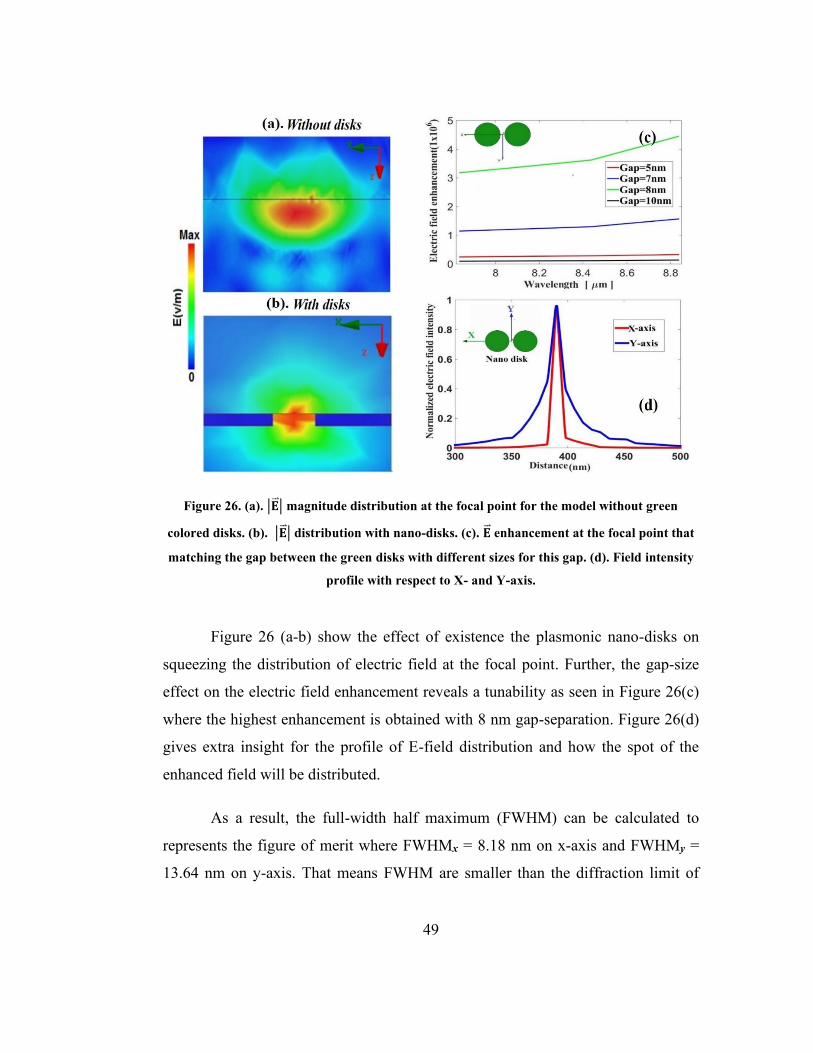
Figure 26. (a). |�⃗� | magnitude distribution at the focal point for the model without green
colored disks. (b). |�⃗� | distribution with nano-disks. (c). �⃗� enhancement at the focal point that
matching the gap between the green disks with different sizes for this gap. (d). Field intensity
profile with respect to X- and Y-axis.
Figure 26 (a-b) show the effect of existence the plasmonic nano-disks on
squeezing the distribution of electric field at the focal point. Further, the gap-size
effect on the electric field enhancement reveals a tunability as seen in Figure 26(c)
where the highest enhancement is obtained with 8 nm gap-separation. Figure 26(d)
gives extra insight for the profile of E-field distribution and how the spot of the
enhanced field will be distributed.
As a result, the full-width half maximum (FWHM) can be calculated to
represents the figure of merit where FWHMx = 8.18 nm on x-axis and FWHMy =
13.64 nm on y-axis. That means FWHM are smaller than the diffraction limit of

50
(0.5𝜆), so this is an appropriate for imaging particles are 1/1000 times smaller than
the wavelength.
4.4. 3D Investigations for the Coupling Between Bright- and Dark-Polaritons
in IR-Regime.
This section shows the strengths and advantages of the Hybrid FEM/TMM
technique that was explained in section (4.2). Briefly, the method can be considered
as a mature numerical platform valid for designing and developing most of dispersive
devices. In field of nanophotonic (or nano-optics), Several applications including
sub-diffraction imaging, hyperlensing, biosensing / fingerprinting, beam steering,
waveguiding, and optoelectronics at Terahertz ~ near-infrared, or even visible light
applications like solar cell [60], have gained momentum recently. Based on that, 3D
modeling/simulation for such nano-scale sensitive devices gives a clear analysis and
insight for the undergoing physics. Backed up by our two previous works, see
sections (4.1) and (4.2), applying the technique in (4.2) onto the model in (4.1) with
3D sweeping as illustrated in Figure 27(a) is implemented in HFSS-environment. As
a result, ability to analyze the dispersion for each direction and exploring the
regarding effects is concluding easily as seen in Figure 27(b~d).
According to the defined dimensions listed in Figure 27(a), there are 6
possible combinations represent the same 512 geometries, but they are different in
sorting. These combinations are [xyZ], [xzY], [yxZ], [yzX], [zxY], and [zyX]. For
instance, in [xyZ]-combination, all (8X) lengths are swept for one width (Y) and one
thickness (Z), then these (8X) sweeping lengths are repeated similarly with the other
widths. As a result, there are 64 sweepings (8X) for each width out of (8Y), hence
these 64 sweepings are replicated with the other thicknesses to form 512 sweepings.
Equation (37) shows [xyZ]-combination in a matrix form where the spectral (rows)
and spatial (columns) sweepings are included.

51
[(𝐹1, 𝑋1) . . (𝐹1, 𝑋8)
: : :(𝐹𝑛, 𝑋1) . . (𝐹𝑛, 𝑋8)
]⏟
𝑌1
… [(𝐹1, 𝑋1) . . (𝐹1, 𝑋8)
: : :(𝐹𝑛, 𝑋1) . . (𝐹𝑛, 𝑋8)
]⏟
𝑌8
⏞ 𝑍1
…… ~
~ …… [(𝐹1, 𝑋1):
(𝐹𝑛, 𝑋1). .
⏟ 𝑌1
… . .(𝐹1, 𝑋8)
:(𝐹𝑛, 𝑋8)
]⏟
𝑌8
⏞ 𝑍8
(37)
These different arrangements are beneficial for analyzing and exploring the
spatial dispersions since the shortest sweeping, for example (x) in [xyZ], governs the
spatial dispersion. In fact, the other two dimensions rather than the governing define
the effect of the whole geometry on this certain dispersion. Namely, for a geometry
(X1, Y1, Z1) in [xyZ] combination, the dispersion will be different than another
dispersion for a geometry has the same length but with different thickness and width
such as (X1, Y5, Z3). The physical interpretation for this is understood based on the
concept of constructive- or distractive-interference. So, the large variation between
the two mentioned geometries in terms of width and thickness leads to large
difference in dispersion for the same lengths (X1) in those geometries. Based on that,
each propagating/governing direction has two spatial dispersion representations such
as the dispersion for X-direction, Figure 27(a), which are extracted from [xyZ]- or
[xzY]-combination.
Also, it’s worthen to explain that the dispersions in K-space as seen in Figure
27(b~d) represent the real parts of three different wave vectors, 𝐾𝑋 , 𝐾𝑌, 𝐾𝑍, according
to the related combination. Each one of these wave vectors is calculated using
equation (36) with respect to the related dimension accordingly. For example, there
will be two kind of the complex wave vectors (𝐾𝑋)± by substituting the given
lengths, and each one of these wave vectors denotes to either the Endfire (𝐾𝑋) + or
Backfire (𝐾𝑋) + propagation according to subwavelength diffraction concept. These

52
two kinds of complex 𝐾𝑋 need sorting process before plotting due to inconsistency
between extracted S-matrices from HFSS and our adopted. The sorting process for
(+) and (-) wave vectors will be done using a certain MatLab-Code, see appendix.
Figure 27. (a). The HFSS-cell for the design involved with sweeping optimetrics at (f=40~52.5
THz,𝛉 = 𝟏𝟎𝐨, 𝛟 = 𝟎𝐨, 𝐠𝐲 = 𝟐𝟓 𝐧𝐦 and 𝛜𝐬𝐢𝐨𝟐 = 𝟐. 𝟐𝟓). The red and blue curved-arrows
illustrate the direct and indirect excitation, respectively. (b). 4D dispersion in K-space with
respect to X-direction where the color-bar represents the frequency-band. It is extracted from
[xyZ]- or [xzY]-combination for first (8) harmonics according to equation (36). (c). the
dispersion relation with respect to Y-direction, and it is plotted based on [yxZ]- or [yzX]-
combination. (d). The dispersion regarding to Z-direction extracted from [zxY]- or [zyX].

53
Likewise, the subwavelength diffractions’ concept is valid also for the other
directions (Y and Z) whenever the diffractive response condition is met where each
real structure has a limited spatial/spectral range; the wavelength less than the
directional gratings (𝜆 ≪ Λ). Also, the higher order harmonics, emerged up from
these diffractions, tend to be evanescent carrying lower energy as the order increases.
In that regard, an issue called optical nonlocality occurring due to the changing from
an ordinary material, on microscopic scale, to HMM on larger scale [10]. Unlike
other techniques that determine the dispersive features based on the effective
concept, and hence they fail to solve optical nonlocality and inaccurate predictions
for the effective media are resulted. Our hybrid technique handling this issue by
considering the harmonic-order, as seen in equation (36), and the resulting rippled
shapes in Figure 27(b~d).
Additionally, analyzing the 3 main planes for the results in Figure 27(b~d)
provides a clear insight for the nature of the generated modes and their coupling and
distributions. Therefore, Figure 28 sketches these planes of view with respect to each
K-space representation in the previous figure. Consequently, hyperbolic features for
HMMs, which are type-I (or volume modes) and type-II (or the surface modes), are
clearly distinguished in these results. Moreover, the edge modes which are well
known as Dyakonov polaritons [61][62], and the coupling or the overlapping
between these two different kinds of modes could be remarkable.

54
Figure 28. 3D depicting of XZ-, YZ-, and XY-plane view for the K-space representations as
seen in Figure 27(b~d). The colors in all plots represent the 4th dimension or the frequency
[THz] as defined in Figure (27).
Based on that, the geometric prospective for the model involved leads to
consider XZ-view plane relates directly to Y-direction and indirectly to the other
directions. Likewise, YZ-view plane is directly related to X-directions while XY-
view plane to Z-direction. Also, it should be mentioned that the length (X-direction)
and the thickness (Z-direction) of both Au and hBN rods are sweeping, but the sweep
for the width (Y-direction) is only the case with hBN. Further, the direct excitation

55
for the model, as shown in Figure 27(a) with red arrow, interacts profusely with Au-
rod and introduces bright (wide peak) modes as we investigated that previously,
section 4.1. Most of these bright modes are diffracted and responsible for indirect
excitation for hBN rod across the gap. Such capacitive trigging is depicted in Figure
27(a) by blue curved arrows.
The interpretation of the results in Figure 28 based on this background could
be summarized into 5 points.
• The bright modes are concentrated/distributed along the surfaces of Au-
rod which means they are surface modes as seen in XZ-view, X-direction.
On the other hand, sweeping the width of hBN rod illustrates that XZ-
view has edge-modes located exactly at the apexes of hBN rod.
• YZ-view confirms the previous interpretation where the explicit surface
modes are presented with Y-direction. So, the two apexes of hBN seem
as hot spots while the longitudinal faces of this rod regard to XZ-view
edge-modes.
• Surprisingly, the type-I hyperbolic mode that is defined as volume mode
takes place with the length spatial dispersion (X-direction) in YZ-view
plane. Namely, the air gap between two rods hosts these modes exactly
closed to the apexes.
• Regarding to Z-direction, no interesting remarks are presented except
with XY-view plane of the model where both kinds of modes (surface
and volume) are overlapping.
• A clear conclusion could be addressed that the distribution of these
dispersive modes is located at the air gap, the inner side of Au-rod, and
the apexes corners of the hBN rod.

56
Along the same lines of analyzing the nature and distributions of the modes,
the distributed energy inside different structures can provide the intrinsic offered
resonances. Hence, tuning the coupling between dark and bright polaritons reveals
that the intrinsic resonances are defined to facilitate designing a sensing device that
fits the optimum conditions such as critical coupling. In fact, matching optimum
sensing requirements is fulfilled when the maximum resonance takes place. In other
words, the exact overlapping between the dark/absorbing modes and the
bright/scattering modes defines the maximum resonance which is well-known as
critical coupling. At this coupling, the ratio between the internal (𝛾𝑖) and the external
damping rates (𝛾𝑒) is unity. In contrast, this ratio is less than 1 for undercoupling
(𝛾𝑖 > 𝛾𝑒), and overcoupling (𝛾𝑖 < 𝛾𝑒 ) according to the theory of resonators [13].
Starting from S-matrices, a comparison pattern between Reflectance (R),
Absorbance, (A), and transmittance (T) is listed and named starting with the smallest
quantity.
• TAR = (R > A) & (R > T) & (A > T).
• ATR = (R > A) & (R > T) & (A < T).
• ART = (R > A) & (R < T) & (A < T).
• TRA = (R < A) & (R > T) & (A > T).
• RAT = (R < A) & (R < T) & (A < T).
• RTA = (R < A) & (R < T) & (A > T).
The corresponding results are shown in Figure 29(a ~ c) for an incident angle
(𝜃 = 10). As seen in these plots, sorting the results as functions of length, width, and
thickness provides a clear vision for the correlation between the intrinsic resonances
and dimensions. From general design prospective, the optimum dimension should
meet the operation point where all these variations are vanished. These conditions
are clearly seen in 29(a ~ c) at the 5th, 7th, and 8th lengths, while the manipulating the
constructive and distractive harmonics interfaces is hard with the width due to the
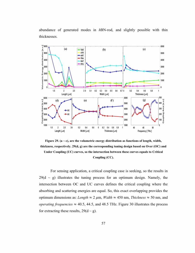
57
abundance of generated modes in hBN-rod, and slightly possible with thin
thicknesses.
Figure 29. (a ~ c), are the volumetric energy distribution as functions of length, width,
thickness, respectively. 29(d, g) are the corresponding tuning design based on Over (OC) and
Under Coupling (UC) curves, so the intersection between these curves equals to Critical
Coupling (CC).
For sensing application, a critical coupling case is seeking, so the results in
29(d ~ g) illustrates the tuning process for an optimum design. Namely, the
intersection between OC and UC curves defines the critical coupling where the
absorbing and scattering energies are equal. So, this exact overlapping provides the
optimum dimensions as: Length ≈ 2 𝜇m, Width ≈ 450 nm, Thickness ≈ 50 nm, and
operating frequencies ≈ 40.5, 44.5, and 48.5 THz. Figure 30 illustrates the process
for extracting these results, 29(d ~ g).

58
Figure 30. Process for Calculating OC- and UC-curves based on Corresponding areas as
function of dimension. The inset under the diagram is an example for Coupling areas as
function of Length (X).
In contrast for the results of broadside-incidence as seen previously (𝜃 = 10),
the endfire excitation at (𝜃 = 80) for the same design will tune-off the critical
coupling between the generated polaritons as shown in Figure 31(a,b). The main
reason can be noticed by comparing plots in 31(c,e), which are type I and II for the
whole involved design at (𝜃 = 80), with the corresponding plots in Figure 28 which
are type I and type II at (𝜃 = 10). The deformation in the hyperbolic features of type-
I and type-II modes explains how much weakness for these modes prevents
overlapping between them. So that leads to concludes that comparison between the
broadside and endfire applied excitation where the endfire has less diffractive or

59
reflective harmonics for trigging and interacting with phonon polaritons in h-BN rod
and air gap.
Figure 31. (a, b). Results for OC (blue) and UC (red) with excitation has (𝛉 = 𝟖𝟎𝐨)
corresponding to the results in 29(d) and 29(g) when 𝛉 = 𝟏𝟎𝐨. Likewise, the other results in
30(c, e) are view planes for K-space dispersions with X, Y, Z-direction and incident angle 𝛉 =
𝟖𝟎𝐨 corresponding to the results in Figure (28).

60
Chapter 5: Summary and Conclusions
The solid background that has been introduced through the first three chapters
could be addressed in one sentence; engineering the interaction between EM waves
and a hosted matter depends on what kind of dispersion-momentum or complex wave
vector is obtained. Further, this important quantity represents how much the
susceptibility of the hosted material is by exposing to a certain EM intensity under
certain conditions. In fact, most of the methods in chapter 3 seeking the best
estimation for this crucial momentum in different circumstances.
For the design explained in section 4.1. the plasmonic gold rod is excited
directly by the incident field and radiates the energy across the h-BN antenna
transversely. A spectrally tunable six orders of magnitude in field enhancement can
be achieved with the introduction of a monolayer of graphene to the gold/h-BN
coupled system. That high amount of enhancement is presented only with volumetric
modes and relatively depends on the width of the h-BN antenna and the enhanced
wavelength to squeeze waves in a small volume. The results shown in this work
indicate that the proposed structure has great potential as a platform for mid- to long-
IR wave sensing and surface enhanced IR absorption spectroscopy devices for the
detection and identification of molecular absorption lines.
Also, another conclusion could be noticed from the published study that is
explained in section 4.2 where a novel hybrid FEM/TMM technique is suggested.
This technique can provide the complex wave vector which is the most important
quantity in studying and designing the dispersive structures. Regardless of the
ingredients or the geometry, 3D modelling of a structure in FEM environment
introduces an accurate prototyping, hence set of governing equations are solved
according to TMM. As a result, complex wave vectors represent both the spectral
and spatial dispersions can be obtained.

61
Unlike the study shown in section 4.1, the design in section 4.3 is carried out
by EMT and represents a metalense which was originally works in visible light but
modified to fit mid infrared. Consequently, a new metalense provides a super-
resolution focusing with high electric-field enhancement. Using InAs as an
alternative to metals reduces losses. The hyperbolic metamaterial allows the lens to
support the propagation of waves with high wave vectors in IR regime. The electric
field at the focal point is enhanced by using two Au nano-disks. The fullwidth half
maximum (FWHM) of the field at the focal point is 8.18nm x 13.64nm on the x-axis
and y-axis, respectively. This high confinement allows to sense or image particles
that are 1/1000 times the wavelength. Such a metalenses may be used for sub-
wavelength imaging and sensing with super resolution and high electric field
enhancement.
Finally, 3D investigations in section 4.4 are related to applying the hybrid
technique, see section 4.2, into the design in section 4.1. In this work, an insightful
analysis for the nature of dispersive modes in IR structure provides a strong
numerical platform to design an optimum IR-sensing device. Therefore, identifying
the nature and distribution of the generated modes can lead to manipulating the
bounded modes and tuning them to the intrinsic resonances. So, defining the
appropriate materials for an interested spectrum and the geometry-restrictions are all
the design-requirements for this platform.
62
References
[1] M. W. McCall, “Classical Mechanics: From Newton to Einstein: A Modern
Introduction: Second Edition,” Class. Mech. From Newt. to Einstein A Mod. Introd.
Second Ed., p. 2020, 2010.
[2] L. J. Prokopeva, J. D. Borneman, and A. V. Kildishev, “Optical dispersion models
for time-domain modeling of metal-dielectric nanostructures,” IEEE Trans. Magn.,
vol. 47, no. 5, pp. 1150–1153, 2011.
[3] C. Huck et al., “Strong coupling between phonon-polaritons and plasmonic
nanorods,” Opt. Express, vol. 24, no. 22, p. 25528, 2016.
[4] A. D. Boardman and K. Marinov, “Electromagnetic energy in a dispersive
metamaterial,” Phys. Rev. B - Condens. Matter Mater. Phys., vol. 73, no. 16, pp. 1–
7, 2006.
[5] M. A. Ordal, R. J. Bell, R. W. Alexander, L. L. Long, and M. R. Querry, “Optical
properties of fourteen metals in the infrared and far infrared: Al, Co, Cu, Au, Fe, Pb,
Mo, Ni, Pd, Pt, Ag, Ti, V, and W,” Appl. Opt., vol. 24, no. 24, p. 4493, 1985.
[6] S. A. Maier, Plasmonics: Fundamentals and applications. 2007.
[7] J. D. Caldwell et al., “Low-loss, infrared and terahertz nanophotonics using surface
phonon polaritons,” Nanophotonics, vol. 4, no. 1, pp. 44–68, 2015.
[8] D. Y. Smith, M. Inokuti, and W. Karstens, “A generalized cauchy dispersion formula
and the refractivity of elemental semiconductors,” J. Phys. Condens. Matter, vol. 13,
no. 17, pp. 3883–3893, 2001.
[9] K. S. Cole and R. H. Cole, “Dispersion and absorption in dielectrics I. Alternating
current characteristics,” J. Chem. Phys., vol. 9, no. 4, pp. 341–351, 1941.

63
[10] R. C. Rumpf, “Engineering the Dispersion and Anisotropy of Periodic
Electromagnetic Structures,” Solid State Phys. - Adv. Res. Appl., vol. 66, pp. 213–
300, 2015.
[11] J. D. Caldwell et al., “Sub-diffractional volume-confined polaritons in the natural
hyperbolic material hexagonal boron nitride,” Nat. Commun., vol. 5, pp. 1–9, 2014.
[12] D. N. Basov, M. M. Fogler, and F. J. García De Abajo, “Polaritons in van der Waals
materials,” Science (80-. )., vol. 354, no. 6309, p. 2020, 2016.
[13] F. Neubrech, C. Huck, K. Weber, A. Pucci, and H. Giessen, “Surface-enhanced
infrared spectroscopy using resonant nanoantennas,” Chem. Rev., vol. 117, no. 7, pp.
5110–5145, 2017.
[14] J. C. Burfoot and G. W. Taylor, Polar dielectrics and their applications. Univ of
California Press, 1979.
[15] G. J. Fiechtner and J. R. Gord, “Absorption and the dimensionless overlap integral
for two-photon excitation,” J. Quant. Spectrosc. Radiat. Transf., vol. 68, no. 5, pp.
543–557, 2001.
[16] P. Ajayan, P. Kim, and K. Banerjee, “Two-dimensional van der Waals materials,”
Phys. Today, vol. 69, no. 9, pp. 38–44, 2016.
[17] E. P. Schoch, W. A. Felsing, G. W. Watt, and F. L. Okell, “General chemistry,”
Analyst, vol. 72, no. 854, pp. 226–227, 1947.
[18] K. S. Novoselov et al., “Electric field in atomically thin carbon films,” Science (80-.
)., vol. 306, no. 5696, pp. 666–669, 2004.
[19] A. Vakil and N. Engheta, “Transformation optics using graphene,” Science (80-. ).,
vol. 332, no. 6035, pp. 1291–1294, 2011.

64
[20] Z. Q. Li et al., “Dirac charge dynamics in graphene by infrared spectroscopy,” Nat.
Phys., vol. 4, no. 7, pp. 532–535, 2008.
[21] X. Luo, T. Qiu, W. Lu, and Z. Ni, “Plasmons in graphene: Recent progress and
applications,” Mater. Sci. Eng. R Reports, vol. 74, no. 11, pp. 351–376, 2013.
[22] J. S. Shin, J. S. Kim, and J. Tae Kim, “Graphene-based hybrid plasmonic modulator,”
J. Opt. (United Kingdom), vol. 17, no. 12, p. 125801, 2015.
[23] S. Dai et al., “Tunable phonon polaritons in atomically thin van der Waals crystals
of boron nitride,” Science (80-. )., vol. 343, no. 6175, pp. 1125–1129, 2014.
[24] E. Franke et al., “In situ infrared and visible-light ellipsometric investigations of
boron nitride thin films at elevated temperatures,” J. Appl. Phys., vol. 84, no. 1, pp.
526–532, 1998.
[25] M. N. O. Sadiku, Numerical techniques in electromagnetics. CRC press, 2000.
[26] F. Manene, E. C. Kinzel, and B. A. Lail, “Finite element eigenmode analysis of
hybrid surface phonon polariton infrared waveguides,” Annu. Rev. Prog. Appl.
Comput. Electromagn., vol. 2014-Janua, pp. 297–302, 2014.
[27] J.-M. Jin, The finite element method in electromagnetics. John Wiley & Sons, 2015.
[28] L. Ansoft, “An introduction to hfss fundamental principles, concepts, and use,”
Ansoft, Pittsburgh, p. 88, 2009.
[29] F. Frezza, F. Mangini, and N. Tedeschi, “Introduction to electromagnetic scattering:
tutorial,” J. Opt. Soc. Am. A, vol. 35, no. 1, p. 163, 2018.
[30] M. Kerker, “The Scattering of Light (New York: Academic),” 1969.
[31] Lord Rayleigh, “X. On the electromagnetic theory of light,” London, Edinburgh,
Dublin Philos. Mag. J. Sci., vol. 12, no. 73, pp. 81–101, 1881.

65
[32] T. Neuman et al., “Importance of Plasmonic Scattering for an Optimal Enhancement
of Vibrational Absorption in SEIRA with Linear Metallic Antennas,” J. Phys. Chem.
C, vol. 119, no. 47, pp. 26652–26662, 2015.
[33] C. L. Cortes, W. Newman, S. Molesky, and Z. Jacob, “Quantum nanophotonics using
hyperbolic metamaterials,” J. Opt. (United Kingdom), vol. 14, no. 6, p. 2020, 2012.
[34] P. Lalanne and J.-P. Hugonin, “High-order effective-medium theory of
subwavelength gratings in classical mounting: application to volume holograms,” J.
Opt. Soc. Am. A, vol. 15, no. 7, p. 1843, 1998.
[35] J. B. Pendry and A. MacKinnon, “Calculation of photon dispersion relations,” Phys.
Rev. Lett., vol. 69, no. 19, p. 2772, 1992.
[36] H. Kitahara, M. W. Takeda, M. Iida, M. Watanabe, K. Sakai, and M. Tani,
“Reflection losses of finite periodic photonic crystals,” Laser Phys., vol. 14, no. 5,
pp. 654–659, 2004.
[37] C. Zhang, F. Qiao, J. Wan, and J. Zi, “Enlargement of nontransmission frequency
range in photonic crystals by using multiple heterostructures,” J. Appl. Phys., vol. 87,
no. 6, pp. 3174–3176, 2000.
[38] R. S. Dubey and D. K. Gautam, “Photonic bandgap analysis in 1D porous silicon
photonic crystals using transfer matrix method,” Optoelectron. Adv. Mater.
Commun., vol. 1, no. 9, pp. 436–441, 2007.
[39] H. Taniyama, “Waveguide structures using one-dimensional photonic crystal,” J.
Appl. Phys., vol. 91, no. 6, pp. 3511–3515, 2002.
[40] A. Alsalhin, M. F. Finch, and B. A. Lail, “Coupling between metallic structure and
phonon polaritons for sensing applications,” no. September 2018, p. 82, 2018.
[41] A. Woessner et al., “Highly confined low-loss plasmons in graphene–boron nitride
heterostructures,” Nat. Mater., vol. 14, no. 4, pp. 421–425, 2015.

66
[42] F. J. Alfaro-Mozaz et al., “Nanoimaging of resonating hyperbolic polaritons in linear
boron nitride antennas,” Nat. Commun., vol. 8, 2017.
[43] R. Marty, A. Mlayah, A. Arbouet, C. Girard, and S. Tripathy, “Plasphonics: local
hybridization of plasmons and phonons,” Opt. Express, vol. 21, no. 4, pp. 4551–4559,
2013.
[44] P. Weis, J. L. Garcia-Pomar, R. Beigang, and M. Rahm, “Hybridization induced
transparency in composites of metamaterials and atomic media,” Opt. Express, vol.
19, no. 23, pp. 23573–23580, 2011.
[45] D. J. Shelton et al., “Strong coupling between nanoscale metamaterials and
phonons,” Nano Lett., vol. 11, no. 5, pp. 2104–2108, 2011.
[46] L. Verslegers, Z. Yu, Z. Ruan, P. B. Catrysse, and S. Fan, “From electromagnetically
induced transparency to superscattering with a single structure: a coupled-mode
theory for doubly resonant structures,” Phys. Rev. Lett., vol. 108, no. 8, p. 83902,
2012.
[47] L. Verslegers, Z. Yu, P. B. Catrysse, and S. Fan, “Temporal coupled-mode theory for
resonant apertures,” JOSA B, vol. 27, no. 10, pp. 1947–1956, 2010.
[48] L. Novotny, “Strong coupling, energy splitting, and level crossings: A classical
perspective,” Am. J. Phys., vol. 78, no. 11, pp. 1199–1202, 2010.
[49] A. Alsalhin and B. Lail, “Determining the dispersive features of nanophotonic
structures based on hybrid fem/tmm technique,” in 2019 International Applied
Computational Electromagnetics Society Symposium in Miami, ACES-Miami 2019,
2019.
[50] R. C. Rumpf, “Improved formulation of scattering matrices for semi-analytical
methods that is consistent with convention,” Prog. Electromagn. Res., vol. 35, pp.
241–261, 2011.

67
[51] P. Yeh, Optical waves in layered media, vol. 95. Wiley Online Library, 1988.
[52] A. W. T-junction, “Getting Started with HFSS :,” vol. 15317, no. May, pp. 724–746,
2003.
[53] P. Li et al., “Optical nanoimaging of hyperbolic surface polaritons at the edges of van
der Waals materials,” Nano Lett., vol. 17, no. 1, pp. 228–235, 2017.
[54] S. Dai et al., “Subdiffractional focusing and guiding of polaritonic rays in a natural
hyperbolic material,” Nat. Commun., vol. 6, no. 1, pp. 1–7, 2015.
[55] M. Kyamo, N. Premkumar, A. Alsalhin, and B. A. Lail, “A Novel Mid-Infrared
Metalens Using a Hyperbolic Metamaterial,” in 2019 International Applied
Computational Electromagnetics Society Symposium in Miami, ACES-Miami 2019,
2019.
[56] V. G. Vesselago, “The electrodynamics of substances with simultaneously negative
values of permittivity and permeability,” Sov. Phys. Usp, vol. 10, no. 4, pp. 509–514,
1968.
[57] J. B. Pendry, “Negative refraction makes a perfect lens,” Phys. Rev. Lett., vol. 85, no.
18, p. 3966, 2000.
[58] C. Ma and Z. Liu, “A super resolution metalens with phase compensation
mechanism,” Appl. Phys. Lett., vol. 96, no. 18, p. 183103, 2010.
[59] F. Peragut et al., “Hyperbolic metamaterials and surface plasmon polaritons,” Optica,
vol. 4, no. 11, pp. 1409–1415, 2017.
[60] T. Low et al., “Polaritons in layered two-dimensional materials,” Nat. Mater., vol.
16, no. 2, pp. 182–194, 2017.
[61] P. Li et al., “Infrared hyperbolic metasurface based on nanostructured van der Waals
materials,” Science (80-. )., vol. 359, no. 6378, pp. 892–896, 2018.

68
[62] Z. Jacob and E. E. Narimanov, “Optical hyperspace for plasmons: Dyakonov states
in metamaterials,” Appl. Phys. Lett., vol. 93, no. 22, p. 221109, 2008.

69
Appendix
The hybrid method described in section 4.2 and 4.4 has an important
procedure could be done using MATLAB environment. So, the related code is
explained in this appendix to give clear insight to the presented results and the
method. The code starts by defining S-matrix data as described in equation (37).
These block matrices are sorted to give 6 combination where each two combinations
define similar results. As a result, there are three main combinations.
A. Defining the Dimensions & Harmonic Orders
In this part of the code, the given dimensions, see Figure 27(a), are introduced to
the code. So, the relevant Code is:
Dx=1e-6.*[1.2566,1.5708,1.75,1.9,2.0944,2.25,2.5,3]; % Length
sz=2e-6; hz=1e-6.*[0.01,0.05,0.075,0.18,0.26,0.38,0.58,1]; Dz=sz+hz; % Thickness
hy=1e-6.*[0.025,0.05,0.1,0.2,0.35,0.48,0.6,0.7]; gy=0.025e-6; % Width
ay=0.1e-6; Dy=hy+gy+ay;
bf=[0 -1 -2 -3 -4 -5 -6 -7]; % Backfire Harmonic-Order
ef=[0 1 2 3 4 5 6 7]; % Endfire Harmonic-Order
B. Complex WaveVectors for Three Main Direction-Based Combinations:
[xyZ], [yzX], [zxY]
The second part of the code represents the main calculations for the complex
wave vectors based on the three main combinations. Therefore, several intercrossed
loops will be used to consider the Harmonic-Order (bf), number of operating
frequencies (rM), the sorted dimensions (cM), and the endfire (+) and backfire (-)
wave vectors. Only [xyZ] combination is detailed below, but the other combinations
have similar procedure.
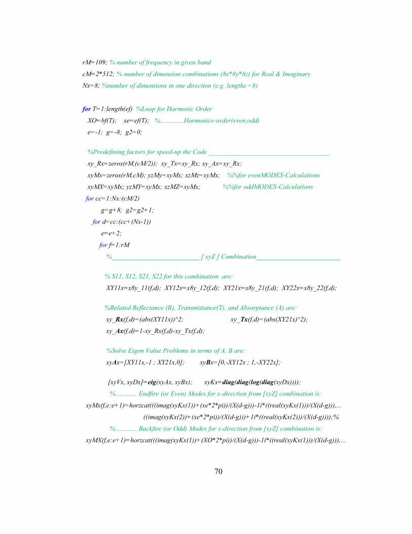
70
rM=109; % number of frequency in given band
cM=2*512; % number of dimension combinations (8x*8y*8z) for Real & Imaginary
Nx=8; %number of dimensions in one direction (e.g. lengths =8)
for T=1:length(ef) %Loop for Harmonic Order
XO=bf(T); xe=ef(T); %..............Harmonics-order(even,odd)
e=-1; g=-8; g2=0;
%Predefining factors for speed-up the Code ____________________________________
xy_Rx=zeros(rM,(cM/2)); xy_Tx=xy_Rx; xy_Ax=xy_Rx;
xyMx=zeros(rM,cM); yzMy=xyMx; xzMz=xyMx; %%for evenMODES-Calculations
xyMX=xyMx; yzMY=xyMx; xzMZ=xyMx; %%for oddMODES-Calculations
for cc=1:Nx:(cM/2)
g=g+8; g2=g2+1;
for d=cc:(cc+(Nx-1))
e=e+2;
for f=1:rM
%__________________________ [ xyZ ] Combination_________________________
% S11, S12, S21, S22 for this combination are:
XY11x=x8y_11(f,d); XY12x=x8y_12(f,d); XY21x=x8y_21(f,d); XY22x=x8y_22(f,d);
%Related Reflectance (R), Transmittance(T), and Absorptance (A) are:
xy_Rx(f,d)=(abs(XY11x))^2; xy_Tx(f,d)=(abs(XY21x)^2);
xy_Ax(f,d)=1-xy_Rx(f,d)-xy_Tx(f,d);
%Solve Eigen Value Problems in terms of A, B are:
xyAx=[XY11x,-1 ; XY21x,0]; xyBx=[0,-XY12x ; 1,-XY22x];
[xyVx, xyDx]=eig(xyAx, xyBx); xyKx=diag(diag(log(diag(xyDx))));
%............. Endfire (or Even) Modes for x-direction from [xyZ] combination is:
xyMx(f,e:e+1)=horzcat(((imag(xyKx(1))+(xe*2*pi))/(X(d-g)))-1i*((real(xyKx(1)))/(X(d-g))),...
((imag(xyKx(2))+(xe*2*pi))/(X(d-g)))+1i*((real(xyKx(2)))/(X(d-g))));%
%............. Backfire (or Odd) Modes for x-direction from [xyZ] combination is:
xyMX(f,e:e+1)=horzcat(((imag(xyKx(1))+(XO*2*pi))/(X(d-g)))-1i*((real(xyKx(1)))/(X(d-g))),...

71
((imag(xyKx(2))+(XO*2*pi))/(X(d-g)))+1i*((real(xyKx(2)))/(X(d-g))));%
end
end
end
xyMDx(1:rM, bf(T):( bf (T)+(cM-1)))=xyMx(1:rM,:); %even Kx
xyMDX(1:rM, bf (T):( bf (T)+(cM-1)))=xyMX(1:rM,:); %odd Kx
end
C. Sorting of Calculated Wave Vectors
The calculations from the past step show the wave vectors as a big matrices where
the endfire (+ harmonics) and the backfire (-harmonics) are listed beside each other,
see the part (f, e:e+1). Therefore, separating the odd order and the even order can
determain the endfire and backfire wave vectors for a certain direction.
xyOx=xyMDx(:,(1:2:end)); xyEx=xyMDx(:,(2:2:end));% ............ [xyZ]
xyOX=xyMDX(:,(1:2:end)); xyEX=xyMDX(:,(2:2:end));
yzOy=yzMDy(:,(1:2:end)); yzEy=yzMDy(:,(2:2:end));% ............ [yzX]
yzOY=yzMDY(:,(1:2:end)); yzEY=yzMDY(:,(2:2:end));
zxOz=zxMDz(:,(1:2:end)); zxEz=zxMDz(:,(2:2:end)); % ............ [xzY]
zxOZ=zxMDZ(:,(1:2:end)); zxEZ=zxMDZ(:,(2:2:end));
%After WaveVector Corrections:-
%(1). Plot K-space for each combination
%(2). Extracting the Dielectric Functions (Epsilon = E): real(E)=(n^2)-(k^2), imag(E)=2(n)(k).
Also: n=[real(K)]/K0, k=[imag(K)]/K0
D. WaveVectors Correction
The resultant wave vectors are inaccurate due to mismatching in the method of
calculation between S-matrix in HFSS-environment, and S-matrix represented in
TMM in the hybrid method, see section 4.2, and section 4.4. Then, the correction

72
step is important to solve this issue, and creating a simple function in MatLab Code
is the next shown part of the whole Code.
function [Ok, Ek] = WVcorrection (K1, K2)
% This function corrects the resultant Complex WaveVectors (K1 & K2) due to
% the mismatching for S-matrix parameters. [Ek] represents the positive
% and/or the biggest one between the inputs:(K1 & K2) while [Ok]= oppesite.
%
% [K1],[K2] are matrices that have rows=frequencies, and columns=dimensions
[rw,cl]=size(K1); Ek=zeros(size(K1)); Ok=Ek;
for i=1:rw % row-counter == Frequencies
for j=1:cl % column-counter == dimension
if (real(K2(i,j))>0) && (real(K1(i,j))<0)
Ek(i,j) = K2(i,j); Ok(i,j) = K1(i,j);
elseif (real(K2(i,j))<0) && (real(K1(i,j))>0)
Ek(i,j) = K1(i,j); Ok(i,j) = K2(i,j);
elseif (real(K2(i,j))>0) && (real(K1(i,j))>0) && (real(K2(i,j))>real(K1(i,j)))
Ek(i,j) = K2(i,j); Ok(i,j) = K1(i,j);
elseif (real(K2(i,j))<0) && (real(K1(i,j))<0) && (real(K2(i,j))>real(K1(i,j)))
Ek(i,j) = K2(i,j); Ok(i,j) = K1(i,j);
elseif (real(K2(i,j))>0) && (real(K1(i,j))>0) && (real(K2(i,j))<real(K1(i,j)))
Ek(i,j) = K1(i,j); Ok(i,j) = K2(i,j);
elseif (real(K2(i,j))<0) && (real(K1(i,j))<0) && (real(K2(i,j))<real(K1(i,j)))
Ek(i,j) = K1(i,j); Ok(i,j) = K2(i,j);
end
end
end
end
Finally, the organized wave vectors are ready for plotting in K-space as seen in figure
27 after this step. Moreover, extracting the directional Dielectric Functions (𝜖) is
possible based on these complex wave vectors where:

73
real (𝜖) = (n^2) - (k^2), and imaginary (𝜖) = 2*(n)*(k).
Also: (n) = [real(K)] / K0, and (k) = [imaginary(K)] / K0.
(K) is complex wave vector in a medium for certain direction while (K0) is the wave
vector in free space.