Embed Size (px)
Citation preview

Analog Filters Using MATLAB

Lars Wanhammar
Analog Filters UsingMATLAB
13

Lars WanhammarDepartment of Electrical EngineeringDivision of Electronics SystemsLinkoping UniversitySE-581 83 [email protected]
ISBN 978-0-387-92766-4 e-ISBN 978-0-387-92767-1DOI 10.1007/978-0-387-92767-1Springer Dordrecht Heidelberg London New York
Library of Congress Control Number: 2008942084
# Springer ScienceþBusiness Media, LLC 2009All rights reserved. This work may not be translated or copied in whole or in part without the writtenpermission of the publisher (Springer ScienceþBusiness Media, LLC, 233 Spring Street, New York,NY 10013, USA), except for brief excerpts in connection with reviews or scholarly analysis. Use inconnection with any form of information storage and retrieval, electronic adaptation, computersoftware, or by similar or dissimilar methodology now known or hereafter developed is forbidden.The use in this publication of trade names, trademarks, service marks, and similar terms, even if theyare not identified as such, is not to be taken as an expression of opinion as to whether or not they aresubject to proprietary rights.
Printed on acid-free paper
Springer is part of Springer ScienceþBusiness Media (www.springer.com)

Preface
This book was written for use in a course at Linkoping University and to aid the
electrical engineer to understand and design analog filters. Most of the advanced
mathematics required for the synthesis of analog filters has been avoided by
providing a set of MATLAB functions that allows sophisticated filters to be
designed. Most of these functions can easily be converted to run under Octave as
well.
The first chapter gives an overview of filter technologies, terminology,
and basic concepts. Approximation of common frequency selective filters
and some more advanced approximations are discussed in Chapter 2. The
reader is recommended to compare the standard approximation with
respect to the group delay, e.g., Example 2.5, and learn to use the corre-
sponding MATLAB functions. Geometrically symmetric frequency trans-
formations are discussed as well as more general synthesis using MATLAB
functions.
Chapter 3 deals with passive LC filters with lumped elements. The
reader may believe that this is an outdated technology. However, it is
still being used and more importantly the theory behind all advanced filter
structures is based on passive LC filters. This is also the case for digital
and switched-capacitor filters. The reader is strongly recommended to
carefully study the principle of maximum power transfer, sensitivity to
element errors, and the implications of Equation (3.26). MATLAB func-
tions are used for the synthesis of ladder and lattice structures. Chapter 4
deals with passive filters with distributed elements. These are useful for
very high-frequency applications, but also in the design of corresponding
wave digital filters.
In Chapter 5, basic circuit elements and their description as one-, two-, and
three-ports are discussed.
Chapter 6 discusses first- and second-order sections using single and
multiple amplifiers. The reader is recommended to study the implication
of the gain-sensitivity product and the two-integrator loop. Chapter 7 dis-
cusses coupled forms and signal scaling, and Chapter 8 discusses various
methods for immitance simulation. Wave active filters are discussed in
v

Chapter 9 and leapfrog filters in Chapter 10. Finally, tuning techniques are
discussed in Chapter 11.
Text with a smaller font is either solved examples or material that the reader
may skip over without losing the main points.
Linkoping
Sweden Lars Wanhammar
vi Preface

Contents
1 Introduction to Analog Filters . . . . . . . . . . . . . . . . . . . . . . . . . . . . . . . 1
1.1 Introduction . . . . . . . . . . . . . . . . . . . . . . . . . . . . . . . . . . . . . . . . 1
1.2 Signals and Signal Carriers. . . . . . . . . . . . . . . . . . . . . . . . . . . . . 1
1.2.1 Analog Signals. . . . . . . . . . . . . . . . . . . . . . . . . . . . . . . . . 2
1.2.2 Continuous-Time Signals . . . . . . . . . . . . . . . . . . . . . . . . 2
1.2.3 Signal Carriers . . . . . . . . . . . . . . . . . . . . . . . . . . . . . . . . . 3
1.2.4 Discrete-Time and Digital Signals. . . . . . . . . . . . . . . . . . 3
1.3 Filter Terminology . . . . . . . . . . . . . . . . . . . . . . . . . . . . . . . . . . . 4
1.3.1 Filter Synthesis . . . . . . . . . . . . . . . . . . . . . . . . . . . . . . . . 4
1.3.2 Filter Realizations . . . . . . . . . . . . . . . . . . . . . . . . . . . . . . 4
1.3.3 Implementation . . . . . . . . . . . . . . . . . . . . . . . . . . . . . . . . 5
1.4 Examples of Applications. . . . . . . . . . . . . . . . . . . . . . . . . . . . . . 6
1.4.1 Carrier Frequency Systems . . . . . . . . . . . . . . . . . . . . . . . 6
1.4.2 Anti-aliasing Filters . . . . . . . . . . . . . . . . . . . . . . . . . . . . . 7
1.4.3 Hard Disk Drives . . . . . . . . . . . . . . . . . . . . . . . . . . . . . . 7
1.5 Analog Filter Technologies . . . . . . . . . . . . . . . . . . . . . . . . . . . . 8
1.5.1 Passive Filters . . . . . . . . . . . . . . . . . . . . . . . . . . . . . . . . . 8
1.5.2 Active Filters . . . . . . . . . . . . . . . . . . . . . . . . . . . . . . . . . . 9
1.5.3 Integrated Analog Filters . . . . . . . . . . . . . . . . . . . . . . . . 9
1.5.4 Technologies for Very High Frequencies . . . . . . . . . . . . 10
1.5.5 Frequency Ranges for Analog Filters . . . . . . . . . . . . . . . 10
1.6 Discrete-Time Filters . . . . . . . . . . . . . . . . . . . . . . . . . . . . . . . . . 11
1.6.1 Switched Capacitor Filters . . . . . . . . . . . . . . . . . . . . . . . 11
1.6.2 Digital Filters. . . . . . . . . . . . . . . . . . . . . . . . . . . . . . . . . . 11
1.7 Analog Filters. . . . . . . . . . . . . . . . . . . . . . . . . . . . . . . . . . . . . . . 12
1.7.1 Frequency Response . . . . . . . . . . . . . . . . . . . . . . . . . . . . 12
1.7.2 Magnitude Function . . . . . . . . . . . . . . . . . . . . . . . . . . . . 12
1.7.3 Attenuation Function . . . . . . . . . . . . . . . . . . . . . . . . . . . 12
1.7.4 Phase Function . . . . . . . . . . . . . . . . . . . . . . . . . . . . . . . . 13
1.7.5 LP, HP, BP, BS, and AP Filters . . . . . . . . . . . . . . . . . . . 14
1.7.6 Phase Delay . . . . . . . . . . . . . . . . . . . . . . . . . . . . . . . . . . . 15
1.7.7 Group Delay . . . . . . . . . . . . . . . . . . . . . . . . . . . . . . . . . . 17
vii

1.8 Transfer Function. . . . . . . . . . . . . . . . . . . . . . . . . . . . . . . . . . . . 18
1.8.1 Poles and Zeros . . . . . . . . . . . . . . . . . . . . . . . . . . . . . . . . 19
1.8.2 Minimum-Phase and Maximum-Phase Filters . . . . . . . . 20
1.9 Impulse Response. . . . . . . . . . . . . . . . . . . . . . . . . . . . . . . . . . . . 21
1.9.1 Impulse Response of an Ideal LP Filter . . . . . . . . . . . . . 21
1.10 Step Response. . . . . . . . . . . . . . . . . . . . . . . . . . . . . . . . . . . . . . . 23
1.11 Problems. . . . . . . . . . . . . . . . . . . . . . . . . . . . . . . . . . . . . . . . . . . 24
2 Synthesis of Analog Filters. . . . . . . . . . . . . . . . . . . . . . . . . . . . . . . . . . 27
2.1 Introduction . . . . . . . . . . . . . . . . . . . . . . . . . . . . . . . . . . . . . . . . 27
2.2 Filter Specification . . . . . . . . . . . . . . . . . . . . . . . . . . . . . . . . . . . 27
2.2.1 Magnitude Function Specification . . . . . . . . . . . . . . . . . 27
2.2.2 Attenuation Specification . . . . . . . . . . . . . . . . . . . . . . . . 28
2.2.3 Group Delay Specification . . . . . . . . . . . . . . . . . . . . . . . 28
2.3 Composite Requirements . . . . . . . . . . . . . . . . . . . . . . . . . . . . . . 29
2.4 Standard LP Approximations . . . . . . . . . . . . . . . . . . . . . . . . . . 30
2.4.1 Butterworth Filters . . . . . . . . . . . . . . . . . . . . . . . . . . . . . 30
2.4.2 Poles and Zeros of Butterworth Filters . . . . . . . . . . . . . . 32
2.4.3 Impulse and Step Response of Butterworth Filters . . . . 34
2.4.4 Chebyshev I Filters . . . . . . . . . . . . . . . . . . . . . . . . . . . . . 36
2.4.5 Poles and Zeros of Chebyshev I Filters . . . . . . . . . . . . . . 39
2.4.6 Reflection Zeros of Chebyshev I Filters . . . . . . . . . . . . . 40
2.4.7 Impulse and Step Response of Chebyshev I Filters . . . . 40
2.4.8 Chebyshev II Filters . . . . . . . . . . . . . . . . . . . . . . . . . . . . 42
2.4.9 Poles and Zeros of Chebyshev II Filters . . . . . . . . . . . . . 45
2.4.10 Impulse and Step Response of Chebyshev II Filters . . . . 46
2.4.11 Cauer Filters . . . . . . . . . . . . . . . . . . . . . . . . . . . . . . . . . . 47
2.4.12 Poles and Zeros of Cauer Filters . . . . . . . . . . . . . . . . . . . 50
2.4.13 Impulse and Step Response of Cauer Filters . . . . . . . . . 50
2.4.14 Comparison of Standard Filters . . . . . . . . . . . . . . . . . . . 53
2.4.15 Design Margin. . . . . . . . . . . . . . . . . . . . . . . . . . . . . . . . . 55
2.4.16 Lowpass Filters with Piecewise-Constant
Stopband Specification . . . . . . . . . . . . . . . . . . . . . . . . . 55
2.5 Miscellaneous Filters . . . . . . . . . . . . . . . . . . . . . . . . . . . . . . . . . 57
2.5.1 Filters with Diminishing Ripple . . . . . . . . . . . . . . . . . . . 57
2.5.2 Multiple Critical Poles. . . . . . . . . . . . . . . . . . . . . . . . . . . 57
2.5.3 Papoulis Monotonic L Filters . . . . . . . . . . . . . . . . . . . . . 57
2.5.4 Halpern Filters . . . . . . . . . . . . . . . . . . . . . . . . . . . . . . . . 57
2.5.5 Parabolic Filters . . . . . . . . . . . . . . . . . . . . . . . . . . . . . . . 57
2.5.6 Linkwitz-Riley Crossover Filters. . . . . . . . . . . . . . . . . . . 57
2.5.7 Hilbert Filters . . . . . . . . . . . . . . . . . . . . . . . . . . . . . . . . . 58
2.6 Delay Approximations . . . . . . . . . . . . . . . . . . . . . . . . . . . . . . . . 58
2.6.1 Gauss Filters . . . . . . . . . . . . . . . . . . . . . . . . . . . . . . . . . . 58
2.6.2 Lerner Filters . . . . . . . . . . . . . . . . . . . . . . . . . . . . . . . . . . 58
2.6.3 Bessel Filters . . . . . . . . . . . . . . . . . . . . . . . . . . . . . . . . . . 58
2.6.4 Lowpass Filters with Equiripple Group Delay . . . . . . . . 60
2.6.5 Equiripple Group Delay Allpass Filters . . . . . . . . . . . . . 60
2.7 Frequency Transformations . . . . . . . . . . . . . . . . . . . . . . . . . . . . 60
viii Contents

2.8 LP-to-HP Transformation . . . . . . . . . . . . . . . . . . . . . . . . . . . . . 60
2.8.1 LP-to-HP Transformation of the Group Delay . . . . . . . 62
2.9 LP-to-BP Transformation . . . . . . . . . . . . . . . . . . . . . . . . . . . . . 64
2.10 LP-to-BS Transformation . . . . . . . . . . . . . . . . . . . . . . . . . . . . . 67
2.11 Piecewise-Constant Stopband Requirement . . . . . . . . . . . . . . . 70
2.12 Equalizing the Group Delay. . . . . . . . . . . . . . . . . . . . . . . . . . . . 72
2.13 Problems. . . . . . . . . . . . . . . . . . . . . . . . . . . . . . . . . . . . . . . . . . . 74
3 Passive Filters . . . . . . . . . . . . . . . . . . . . . . . . . . . . . . . . . . . . . . . . . . . 77
3.1 Introduction . . . . . . . . . . . . . . . . . . . . . . . . . . . . . . . . . . . . . . . . 77
3.2 Resonance Circuits . . . . . . . . . . . . . . . . . . . . . . . . . . . . . . . . . . . 77
3.2.1 Q Factor of Coils. . . . . . . . . . . . . . . . . . . . . . . . . . . . . . . 77
3.2.2 Q Factor for Capacitors . . . . . . . . . . . . . . . . . . . . . . . . . 78
3.3 Doubly Terminated LC Filters. . . . . . . . . . . . . . . . . . . . . . . . . . 79
3.3.1 Maximum Power Transfer . . . . . . . . . . . . . . . . . . . . . . . 79
3.3.2 Insertion Loss . . . . . . . . . . . . . . . . . . . . . . . . . . . . . . . . . 79
3.3.3 Doubly Resistively Terminated Lossless Networks . . . . 80
3.3.4 Broadband Matching . . . . . . . . . . . . . . . . . . . . . . . . . . . 80
3.3.5 Reflection Function. . . . . . . . . . . . . . . . . . . . . . . . . . . . . 81
3.3.6 Characteristic Function . . . . . . . . . . . . . . . . . . . . . . . . . . 81
3.3.7 Feldtkeller’s Equation . . . . . . . . . . . . . . . . . . . . . . . . . . . 82
3.3.8 Sensitivity . . . . . . . . . . . . . . . . . . . . . . . . . . . . . . . . . . . . 82
3.3.9 Element Errors in Doubly Terminated Filters . . . . . . . . 86
3.3.10 Design of Doubly Terminated Filters . . . . . . . . . . . . . . . 88
3.4 Lowpass Ladder Structures . . . . . . . . . . . . . . . . . . . . . . . . . . . . 88
3.4.1 RCLM One-Ports . . . . . . . . . . . . . . . . . . . . . . . . . . . . . . 89
3.4.2 Generic Sections . . . . . . . . . . . . . . . . . . . . . . . . . . . . . . . 89
3.4.3 Lowpass Ladder Structures without Finite Zeros. . . . . . 91
3.4.4 Lowpass Ladder Structures with Finite Zeros . . . . . . . . 92
3.4.5 Design of Lowpass LC Ladder Filters . . . . . . . . . . . . . . 93
3.5 Frequency Transformations . . . . . . . . . . . . . . . . . . . . . . . . . . . . 98
3.5.1 Changing the Impedance Level . . . . . . . . . . . . . . . . . . . . 99
3.5.2 Changing the Frequency Range . . . . . . . . . . . . . . . . . . . 100
3.5.3 LP-to-HP Transformation. . . . . . . . . . . . . . . . . . . . . . . . 100
3.5.4 Multiplexers. . . . . . . . . . . . . . . . . . . . . . . . . . . . . . . . . . . 102
3.5.5 LP-BP Transformation . . . . . . . . . . . . . . . . . . . . . . . . . . 103
3.5.6 LP-BS Transformation . . . . . . . . . . . . . . . . . . . . . . . . . . 107
3.6 Network Transformations . . . . . . . . . . . . . . . . . . . . . . . . . . . . . 107
3.6.1 Dual Networks . . . . . . . . . . . . . . . . . . . . . . . . . . . . . . . . 107
3.6.2 Symmetrical and Antimetrical Networks . . . . . . . . . . . . 109
3.6.3 Reciprocity . . . . . . . . . . . . . . . . . . . . . . . . . . . . . . . . . . . 109
3.6.4 Bartlett’s Bisection Theorem . . . . . . . . . . . . . . . . . . . . . . 110
3.6.5 Delta-Star Transformations . . . . . . . . . . . . . . . . . . . . . . 110
3.6.6 Norton Transformations . . . . . . . . . . . . . . . . . . . . . . . . . 111
3.6.7 Impedance Transformations . . . . . . . . . . . . . . . . . . . . . . 111
3.6.8 Transformations to Absorb Parasitic Capacitance . . . . . 113
3.6.9 Minimum-Inductor Filters . . . . . . . . . . . . . . . . . . . . . . . 114
3.7 Lattice Filters . . . . . . . . . . . . . . . . . . . . . . . . . . . . . . . . . . . . . . . 116
3.7.1 Symmetrical Lattice Structures . . . . . . . . . . . . . . . . . . . . 117
Contents ix

3.7.2 Synthesis of Lattice Reactances. . . . . . . . . . . . . . . . . . . . 117
3.7.3 Element Sensitivity . . . . . . . . . . . . . . . . . . . . . . . . . . . . . 118
3.7.4 Bartlett and Brune’s Theorem . . . . . . . . . . . . . . . . . . . . . 118
3.7.5 Bridged-T Networks . . . . . . . . . . . . . . . . . . . . . . . . . . . . 119
3.7.6 Half-Lattices . . . . . . . . . . . . . . . . . . . . . . . . . . . . . . . . . . 119
3.7.7 Reactance One-Ports . . . . . . . . . . . . . . . . . . . . . . . . . . . . 120
3.8 Allpass Filters. . . . . . . . . . . . . . . . . . . . . . . . . . . . . . . . . . . . . . . 121
3.8.1 Constant-R Lattice Filters. . . . . . . . . . . . . . . . . . . . . . . . 122
3.8.2 Constant-R Bridged-T Sections. . . . . . . . . . . . . . . . . . . . 122
3.8.3 Constant-R Right-L and Left-L Sections . . . . . . . . . . . . 122
3.8.4 Equalizing the Group Delay . . . . . . . . . . . . . . . . . . . . . . 123
3.8.5 Attenuation Equalizing . . . . . . . . . . . . . . . . . . . . . . . . . . 124
3.9 Electromechanical Filters . . . . . . . . . . . . . . . . . . . . . . . . . . . . . . 124
3.9.1 Mechanical Filters . . . . . . . . . . . . . . . . . . . . . . . . . . . . . . 124
3.9.2 Crystal Filters . . . . . . . . . . . . . . . . . . . . . . . . . . . . . . . . . 126
3.9.3 Ceramic Filters . . . . . . . . . . . . . . . . . . . . . . . . . . . . . . . . 127
3.9.4 Surface Acoustic Wave Filters. . . . . . . . . . . . . . . . . . . . . 127
3.9.5 Bulk Acoustic Wave Filters. . . . . . . . . . . . . . . . . . . . . . . 128
3.10 Problems. . . . . . . . . . . . . . . . . . . . . . . . . . . . . . . . . . . . . . . . . . . 129
4 Filters with Distributed Elements . . . . . . . . . . . . . . . . . . . . . . . . . . . . . 133
4.1 Introduction . . . . . . . . . . . . . . . . . . . . . . . . . . . . . . . . . . . . . . . . 133
4.2 Transmission Lines. . . . . . . . . . . . . . . . . . . . . . . . . . . . . . . . . . . 133
4.2.1 Wave Description . . . . . . . . . . . . . . . . . . . . . . . . . . . . . . 135
4.2.2 Chain Matrix for Transmission Lines . . . . . . . . . . . . . . . 135
4.2.3 Lossless Transmission Lines . . . . . . . . . . . . . . . . . . . . . . 136
4.2.4 Richards’ Variable. . . . . . . . . . . . . . . . . . . . . . . . . . . . . . 136
4.2.5 Unit Elements . . . . . . . . . . . . . . . . . . . . . . . . . . . . . . . . . 137
4.3 Microstrip and Striplines . . . . . . . . . . . . . . . . . . . . . . . . . . . . . . 138
4.3.1 Stripline . . . . . . . . . . . . . . . . . . . . . . . . . . . . . . . . . . . . . . 138
4.3.2 Microstrip . . . . . . . . . . . . . . . . . . . . . . . . . . . . . . . . . . . . 138
4.3.3 MIC and MMIC Microstrip Filters . . . . . . . . . . . . . . . . 139
4.4 Commensurate-Length Transmission Line Filters. . . . . . . . . . . 139
4.4.1 Richards’ Structures . . . . . . . . . . . . . . . . . . . . . . . . . . . . 140
4.5 Synthesis of Richards’ Filters. . . . . . . . . . . . . . . . . . . . . . . . . . . 140
4.5.1 Richards’ Filters with Maximally Flat
Passband . . . . . . . . . . . . . . . . . . . . . . . . . . . . . . . . . . . . . 141
4.5.2 Richards’ Filters with Equiripple Passband . . . . . . . . . . 141
4.5.3 Implementation of Richards’ Structures . . . . . . . . . . . . . 143
4.6 Ladder Filters . . . . . . . . . . . . . . . . . . . . . . . . . . . . . . . . . . . . . . . 144
4.7 Ladder Filters with Inserted Unit Elements. . . . . . . . . . . . . . . . 144
4.7.1 Kuroda-Levy Identities . . . . . . . . . . . . . . . . . . . . . . . . . . 145
4.8 Coupled Resonators Filters . . . . . . . . . . . . . . . . . . . . . . . . . . . . 148
4.8.1 Immitance Inverters. . . . . . . . . . . . . . . . . . . . . . . . . . . . . 148
4.8.2 BP Filters Using Capacitively Coupled
Resonators. . . . . . . . . . . . . . . . . . . . . . . . . . . . . . . . . . . . 150
4.9 Coupled Line Filters. . . . . . . . . . . . . . . . . . . . . . . . . . . . . . . . . . 150
4.9.1 Parallel-Coupled Line Filters . . . . . . . . . . . . . . . . . . . . . 151
4.9.2 Hairpin-Line Bandpass Filters . . . . . . . . . . . . . . . . . . . . 151
x Contents

4.9.3 Interdigital Bandpass Filters . . . . . . . . . . . . . . . . . . . . . . 152
4.9.4 Combline Filters . . . . . . . . . . . . . . . . . . . . . . . . . . . . . . . 152
4.10 Problems. . . . . . . . . . . . . . . . . . . . . . . . . . . . . . . . . . . . . . . . . . . 152
5 Basic Circuit Elements . . . . . . . . . . . . . . . . . . . . . . . . . . . . . . . . . . . . . 155
5.1 Introduction . . . . . . . . . . . . . . . . . . . . . . . . . . . . . . . . . . . . . . . . 155
5.2 Passive and Active n-Ports . . . . . . . . . . . . . . . . . . . . . . . . . . . . . 155
5.3 Passive and Active One-Ports. . . . . . . . . . . . . . . . . . . . . . . . . . . 156
5.3.1 Passive One-Ports . . . . . . . . . . . . . . . . . . . . . . . . . . . . . . 156
5.3.2 Active One-Ports . . . . . . . . . . . . . . . . . . . . . . . . . . . . . . . 156
5.4 Two-Ports . . . . . . . . . . . . . . . . . . . . . . . . . . . . . . . . . . . . . . . . . . 156
5.4.1 Chain Matrix . . . . . . . . . . . . . . . . . . . . . . . . . . . . . . . . . . 157
5.4.2 Impedance and Admittance Matrices . . . . . . . . . . . . . . . 158
5.4.3 Passive Two-Ports . . . . . . . . . . . . . . . . . . . . . . . . . . . . . . 158
5.4.4 Active Two-Ports. . . . . . . . . . . . . . . . . . . . . . . . . . . . . . . 159
5.5 Three-Ports. . . . . . . . . . . . . . . . . . . . . . . . . . . . . . . . . . . . . . . . . 161
5.5.1 Passive Three-Ports . . . . . . . . . . . . . . . . . . . . . . . . . . . . . 161
5.5.2 Active Three-Ports. . . . . . . . . . . . . . . . . . . . . . . . . . . . . . 161
5.6 Operational Amplifiers. . . . . . . . . . . . . . . . . . . . . . . . . . . . . . . . 161
5.6.1 Small-Signal Model of Operational Amplifiers. . . . . . . . 162
5.6.2 Implementation of an Operational Amplifier . . . . . . . . . 164
5.7 Transconductors. . . . . . . . . . . . . . . . . . . . . . . . . . . . . . . . . . . . . 164
5.7.1 Transconductance Feedback Amplifiers . . . . . . . . . . . . . 165
5.7.2 Small-Signal Model for Transconductors . . . . . . . . . . . . 165
5.7.3 Implementation of a Transconductor . . . . . . . . . . . . . . . 166
5.8 Current Conveyors . . . . . . . . . . . . . . . . . . . . . . . . . . . . . . . . . . . 166
5.8.1 Current Conveyor I (CCI) . . . . . . . . . . . . . . . . . . . . . . . 167
5.8.2 Current Conveyor II (CCII) . . . . . . . . . . . . . . . . . . . . . . 167
5.8.3 Current Conveyor III (CCIII) . . . . . . . . . . . . . . . . . . . . . 167
5.8.4 Small-Signal Model for Current Conveyor II . . . . . . . . . 167
5.8.5 CMOS Implementation of a CCII– . . . . . . . . . . . . . . . . 168
5.9 Realization of Two-Ports . . . . . . . . . . . . . . . . . . . . . . . . . . . . . . 168
5.9.1 Realization of Controlled Sources: Amplifiers . . . . . . . . 168
5.9.2 Realization of Integrators . . . . . . . . . . . . . . . . . . . . . . . . 170
5.9.3 Realization of Immitance Inverters and Converters . . . . 175
5.10 Realization of One-Ports . . . . . . . . . . . . . . . . . . . . . . . . . . . . . . 176
5.10.1 Integrated Resistors. . . . . . . . . . . . . . . . . . . . . . . . . . . . . 176
5.10.2 Differential Miller Integrators. . . . . . . . . . . . . . . . . . . . . 178
5.10.3 Integrated Capacitors . . . . . . . . . . . . . . . . . . . . . . . . . . . 179
5.10.4 Inductors . . . . . . . . . . . . . . . . . . . . . . . . . . . . . . . . . . . . . 180
5.10.5 FDNRs . . . . . . . . . . . . . . . . . . . . . . . . . . . . . . . . . . . . . . 183
5.11 Problems . . . . . . . . . . . . . . . . . . . . . . . . . . . . . . . . . . . . . . . . . . 183
6 First- and Second-Order Sections. . . . . . . . . . . . . . . . . . . . . . . . . . . . . 187
6.1 Introduction . . . . . . . . . . . . . . . . . . . . . . . . . . . . . . . . . . . . . . . . 187
6.2 First-Order Sections . . . . . . . . . . . . . . . . . . . . . . . . . . . . . . . . . . 187
6.2.1 First-Order LP Section . . . . . . . . . . . . . . . . . . . . . . . . . . 187
6.2.2 First-Order HP Section . . . . . . . . . . . . . . . . . . . . . . . . . . 188
6.2.3 First-Order AP Section . . . . . . . . . . . . . . . . . . . . . . . . . . 188
6.3 Realization of First-Order Sections . . . . . . . . . . . . . . . . . . . . . . 189
Contents xi

6.4 Second-Order Sections . . . . . . . . . . . . . . . . . . . . . . . . . . . . . . . . 190
6.4.1 Second-Order LP Section . . . . . . . . . . . . . . . . . . . . . . . . 190
6.4.2 Second-Order HP Section . . . . . . . . . . . . . . . . . . . . . . . . 192
6.4.3 Second-Order LP-Notch Section. . . . . . . . . . . . . . . . . . . 192
6.4.4 Second-Order HP-Notch Section . . . . . . . . . . . . . . . . . . 193
6.4.5 Second-Order BP Section . . . . . . . . . . . . . . . . . . . . . . . . 193
6.4.6 Element Sensitivity . . . . . . . . . . . . . . . . . . . . . . . . . . . . . 194
6.4.7 Gain-Sensitivity Product . . . . . . . . . . . . . . . . . . . . . . . . . 195
6.4.8 Amplifiers with Finite Bandwidth. . . . . . . . . . . . . . . . . . 196
6.4.9 Comparison of Sections. . . . . . . . . . . . . . . . . . . . . . . . . . 196
6.5 Single-Amplifier Sections . . . . . . . . . . . . . . . . . . . . . . . . . . . . . . 196
6.5.1 RC Networks . . . . . . . . . . . . . . . . . . . . . . . . . . . . . . . . . . 197
6.5.2 Gain-Sensitivity Product for SAB . . . . . . . . . . . . . . . . . . 197
6.5.3 Sections with Negative Feedback . . . . . . . . . . . . . . . . . . 197
6.5.4 NF2 AP Section. . . . . . . . . . . . . . . . . . . . . . . . . . . . . . . . 204
6.5.5 Sections with Positive Feedback . . . . . . . . . . . . . . . . . . . 204
6.5.6 ENF Sections. . . . . . . . . . . . . . . . . . . . . . . . . . . . . . . . . . 209
6.5.7 Complementary Sections. . . . . . . . . . . . . . . . . . . . . . . . . 211
6.6 Transconductor-Based Sections . . . . . . . . . . . . . . . . . . . . . . . . . 211
6.7 GIC-Based Sections . . . . . . . . . . . . . . . . . . . . . . . . . . . . . . . . . . 212
6.7.1 GIC LP Section . . . . . . . . . . . . . . . . . . . . . . . . . . . . . . . . 214
6.7.2 GIC LP-Notch Section . . . . . . . . . . . . . . . . . . . . . . . . . . 214
6.7.3 GIC HP Section. . . . . . . . . . . . . . . . . . . . . . . . . . . . . . . . 214
6.7.4 GIC HP-Notch Section . . . . . . . . . . . . . . . . . . . . . . . . . . 214
6.7.5 GIC BP Section . . . . . . . . . . . . . . . . . . . . . . . . . . . . . . . . 214
6.7.6 GIC AP Section. . . . . . . . . . . . . . . . . . . . . . . . . . . . . . . . 214
6.8 Two-Integrator Loops . . . . . . . . . . . . . . . . . . . . . . . . . . . . . . . . 215
6.8.1 Two-Integrator Loops with Lossless Integrators . . . . . . 215
6.8.2 Kerwin-Huelsman-Newcomb Section . . . . . . . . . . . . . . . 215
6.8.3 Transposed Two-Integrator Loop. . . . . . . . . . . . . . . . . . 217
6.8.4 Two-Integrator Loops with Lossy Integrators . . . . . . . . 218
6.8.5 Tow-Thomas Section. . . . . . . . . . . . . . . . . . . . . . . . . . . . 218
6.8.6 Akerberg-Mossberg Section . . . . . . . . . . . . . . . . . . . . . . 220
6.9 Amplifiers with Low GB Sensitivity . . . . . . . . . . . . . . . . . . . . . . 221
6.9.1 Differential Two-Integrator Loops . . . . . . . . . . . . . . . . . 222
6.9.2 Transconductor Based on Two-Integrator Loops . . . . . 222
6.9.3 Current Conveyors-Based Sections . . . . . . . . . . . . . . . . . 223
6.10 Sections with Finite Zeros . . . . . . . . . . . . . . . . . . . . . . . . . . . . . 224
6.10.1 Summing of Node Signals . . . . . . . . . . . . . . . . . . . . . . . . 225
6.10.2 Injection of the Input Signal . . . . . . . . . . . . . . . . . . . . . . 225
6.11 Problems. . . . . . . . . . . . . . . . . . . . . . . . . . . . . . . . . . . . . . . . . . . 227
7 Coupled Forms . . . . . . . . . . . . . . . . . . . . . . . . . . . . . . . . . . . . . . . . . . . 233
7.1 Introduction . . . . . . . . . . . . . . . . . . . . . . . . . . . . . . . . . . . . . . . . 233
7.2 Taxonomy for Analog Filters. . . . . . . . . . . . . . . . . . . . . . . . . . . 234
7.2.1 Coupled Forms . . . . . . . . . . . . . . . . . . . . . . . . . . . . . . . . 234
7.2.2 Simulation of Ladder Structures . . . . . . . . . . . . . . . . . . . 234
7.3 Cascade Form. . . . . . . . . . . . . . . . . . . . . . . . . . . . . . . . . . . . . . . 235
7.3.1 Optimization of Dynamic Range . . . . . . . . . . . . . . . . . . 236
xii Contents

7.3.2 Thermal Noise . . . . . . . . . . . . . . . . . . . . . . . . . . . . . . . . . 236
7.3.3 Noise in Amplifiers . . . . . . . . . . . . . . . . . . . . . . . . . . . . . 237
7.3.4 Noise in Passive and Active Filters . . . . . . . . . . . . . . . . . 238
7.3.5 Distortion . . . . . . . . . . . . . . . . . . . . . . . . . . . . . . . . . . . . 238
7.3.6 Pairing of Poles and Zeros. . . . . . . . . . . . . . . . . . . . . . . . 238
7.3.7 Ordering of Sections . . . . . . . . . . . . . . . . . . . . . . . . . . . . 239
7.3.8 Optimizing the Section Gain . . . . . . . . . . . . . . . . . . . . . . 240
7.3.9 Scaling of Internal Nodes in Sections . . . . . . . . . . . . . . . 241
7.3.10 LTC1562 and LTC1560. . . . . . . . . . . . . . . . . . . . . . . . . . 244
7.4 Parallel Form . . . . . . . . . . . . . . . . . . . . . . . . . . . . . . . . . . . . . . . 245
7.5 Multiple-Feedback Forms . . . . . . . . . . . . . . . . . . . . . . . . . . . . . 245
7.5.1 Follow-the-Leader-Feedback Form(FLF) . . . . . . . . . . . 246
7.5.2 Inverse Follow-the-Leader-Feedback Form . . . . . . . . . . 249
7.5.3 Minimum Sensitivity Form . . . . . . . . . . . . . . . . . . . . . . . 250
7.6 Transconductor-Based Coupled Forms . . . . . . . . . . . . . . . . . . . 250
7.6.1 Inverse Follow-the-Leader-Feedback Form . . . . . . . . . . 250
7.6.2 Finite Transmission Zeros. . . . . . . . . . . . . . . . . . . . . . . . 251
7.7 Problems. . . . . . . . . . . . . . . . . . . . . . . . . . . . . . . . . . . . . . . . . . . 252
8 Immitance Simulation . . . . . . . . . . . . . . . . . . . . . . . . . . . . . . . . . . . . . 253
8.1 Introduction . . . . . . . . . . . . . . . . . . . . . . . . . . . . . . . . . . . . . . . . 253
8.2 PIC-Based Simulation . . . . . . . . . . . . . . . . . . . . . . . . . . . . . . . . 253
8.3 Gyrator-Based Simulation . . . . . . . . . . . . . . . . . . . . . . . . . . . . . 254
8.3.1 Transconductor-Based Gyrator-C Filters . . . . . . . . . . . . 255
8.3.2 CCII-Based Gyrator-C Filters. . . . . . . . . . . . . . . . . . . . . 255
8.4 Gorski-Popiel’S Method . . . . . . . . . . . . . . . . . . . . . . . . . . . . . . 256
8.5 Bruton’s Method . . . . . . . . . . . . . . . . . . . . . . . . . . . . . . . . . . . . 259
8.6 Problems. . . . . . . . . . . . . . . . . . . . . . . . . . . . . . . . . . . . . . . . . . . 260
9 Wave Active Filters . . . . . . . . . . . . . . . . . . . . . . . . . . . . . . . . . . . . . . . 263
9.1 Introduction . . . . . . . . . . . . . . . . . . . . . . . . . . . . . . . . . . . . . . . . 263
9.2 Generalized Wave Variables. . . . . . . . . . . . . . . . . . . . . . . . . . . . 263
9.2.1 Wave Transmission Matrix . . . . . . . . . . . . . . . . . . . . . . . 264
9.2.2 Chain Scattering Matrix . . . . . . . . . . . . . . . . . . . . . . . . . 264
9.2.3 Generalized Scattering Matrix . . . . . . . . . . . . . . . . . . . . 264
9.2.4 Voltage Scattering Matrix . . . . . . . . . . . . . . . . . . . . . . . . 264
9.3 Interconnection of Wave Two-Ports . . . . . . . . . . . . . . . . . . . . . 266
9.4 Elementary Wave Two-Ports . . . . . . . . . . . . . . . . . . . . . . . . . . . 266
9.5 Higher-Order Wave One-Ports. . . . . . . . . . . . . . . . . . . . . . . . . . 268
9.6 Circulator-Tree Wave Active Filters . . . . . . . . . . . . . . . . . . . . . 270
9.7 Realization of Wave Two-Ports . . . . . . . . . . . . . . . . . . . . . . . . . 271
9.7.1 Realization of a Generic Wave Two-Port . . . . . . . . . . . . 271
9.7.2 Differential Wave Two-Port . . . . . . . . . . . . . . . . . . . . . . 272
9.8 Realization of Wave Active Filters . . . . . . . . . . . . . . . . . . . . . . 273
9.9 Power Complementarity. . . . . . . . . . . . . . . . . . . . . . . . . . . . . . . 273
9.10 Alternative Approach. . . . . . . . . . . . . . . . . . . . . . . . . . . . . . . . . 274
9.11 Problems. . . . . . . . . . . . . . . . . . . . . . . . . . . . . . . . . . . . . . . . . . . 275
10 Topological Simulation . . . . . . . . . . . . . . . . . . . . . . . . . . . . . . . . . . . . 277
10.1 Introduction . . . . . . . . . . . . . . . . . . . . . . . . . . . . . . . . . . . . . . . . 277
Contents xiii

10.2 LP Filters Without Finite Zeros. . . . . . . . . . . . . . . . . . . . . . . . . 277
10.2.1 Lowpass Leapfrog Filters . . . . . . . . . . . . . . . . . . . . . . . 278
10.2.2 Realization of the Signal-Flow Graph . . . . . . . . . . . . . 279
10.2.3 Scaling of Signal Levels . . . . . . . . . . . . . . . . . . . . . . . . . 282
10.3 Geometrically Symmetric BP Leapfrog Filters . . . . . . . . . . . . . 283
10.4 Lowpass Filters Realized with Transconductors . . . . . . . . . . . . 283
10.5 LP Filters with Finite Zeros . . . . . . . . . . . . . . . . . . . . . . . . . . . . 284
10.5.1 Odd-Order Lowpass Filters with Finite Zeros . . . . . . . 285
10.5.2 Even-Order Lowpass Filters with Finite Zeros . . . . . . . 287
10.6 Problems. . . . . . . . . . . . . . . . . . . . . . . . . . . . . . . . . . . . . . . . . . . 289
11 Tuning Techniques . . . . . . . . . . . . . . . . . . . . . . . . . . . . . . . . . . . . . . . . 291
11.1 Introduction . . . . . . . . . . . . . . . . . . . . . . . . . . . . . . . . . . . . . . . . 291
11.2 Component Errors . . . . . . . . . . . . . . . . . . . . . . . . . . . . . . . . . . . 291
11.2.1 Absolute Component Errors . . . . . . . . . . . . . . . . . . . . . 291
11.2.2 Ratio Errors. . . . . . . . . . . . . . . . . . . . . . . . . . . . . . . . . . 292
11.2.3 Dummy Components . . . . . . . . . . . . . . . . . . . . . . . . . . 292
11.3 Trimming . . . . . . . . . . . . . . . . . . . . . . . . . . . . . . . . . . . . . . . . . . 293
11.3.1 Trimming of Second-Order Sections . . . . . . . . . . . . . . . 294
11.3.2 LC Filters. . . . . . . . . . . . . . . . . . . . . . . . . . . . . . . . . . . . 296
11.4 On-Line Tuning . . . . . . . . . . . . . . . . . . . . . . . . . . . . . . . . . . . . . 296
11.4.1 Pseudo-on-Line Tuning . . . . . . . . . . . . . . . . . . . . . . . . . 296
11.4.2 Master-Slave Frequency Tuning . . . . . . . . . . . . . . . . . . 296
11.4.3 Master-Slave Q Factor Tuning . . . . . . . . . . . . . . . . . . . 298
11.5 Off-Line Tuning . . . . . . . . . . . . . . . . . . . . . . . . . . . . . . . . . . . . . 300
11.5.1 Tuning of Composite Structures . . . . . . . . . . . . . . . . . . 300
11.5.2 Parasitic Effects . . . . . . . . . . . . . . . . . . . . . . . . . . . . . . . 301
11.6 Problems. . . . . . . . . . . . . . . . . . . . . . . . . . . . . . . . . . . . . . . . . . . 302
References . . . . . . . . . . . . . . . . . . . . . . . . . . . . . . . . . . . . . . . . . . . . . . . . . . 305
Toolbox for Analog Filters . . . . . . . . . . . . . . . . . . . . . . . . . . . . . . . . . . . . . 309
Index . . . . . . . . . . . . . . . . . . . . . . . . . . . . . . . . . . . . . . . . . . . . . . . . . . . . . . 311
xiv Contents

Note to Instructors
The solutions manual for the book can be found on the author’s webpage at
http://www.es.isy.liu.se/publications/books/Analog Filters Using MATLAB/.
Supplementary information can also be found on the author’s webpage.
xv

Chapter 1
Introduction to Analog Filters
1.1 Introduction
Signal processing techniques involve methods to
extract information from various types of signal
sources but also methods to protect, store, and
retrieve the information at a later date. In, for
example, a telecommunication system we are inter-
ested in transmitting information from one place to
another, whereas in other applications, e.g., MP3
players, we are interested in efficient storing and
retrieving of information. Note that storing infor-
mation for later retrieval can be viewed as transmit-
ting the information over a transmission channel
with an arbitrary long time delay. In many cases,
for example in the MP3 format, signal processing
techniques have been used to remove nonaudible
(redundant) information in order to reduce the
amount of information that needs to be stored.
In, for example, a radio system, we need to gen-
erate different types of signals and modify the sig-
nals so that the information can be transmitted over
a radio channel, e.g., by frequency modulation of a
high-frequency carrier. Analog filters are key com-
ponents in these applications.
Figure 1.1 illustrates a simple digital transmis-
sion system where analog filters are key compo-
nents. Computer A acts as a digital signal source
that generates a sequence of ASCII symbols. The
symbols are represented by 8-bit words. In order to
transmit a symbol over a telephone line, we must
represent the bits in the symbol with a physical
signal carrier that is suitable for the transmission
channel at hand. Here we use a sinusoidal voltage
with two different frequencies as signal carrier and
use so-called frequency shift keying for representing
the information.
In modem A (modulator/demodulator), we let a
‘‘zero’’ bit correspond to 980Hz and a ‘‘one’’ correspond
to 1180 Hz. Hence, modem B has to determine if the
received frequency is 980 or 1180 Hz in order to deter-
mine if a zero or one was transmitted. Two bandpass
filters that let either of the sinusoidal signals pass can be
used to resolve the frequency of the received signal by
comparing the amplitudes of outputs of the two filters.
In a similarway,modemB sends information tomodem
A, but instead uses the frequencies 1650 and 1850 Hz.
Hence, filtering is an essential part of the modems.
The transmission system discussed above is now
outdated. However, modern transmission systems
with higher transmission capacity use similar tech-
niques. For example, high-definition TV (HDTV),
wireless local network (WLAN), and asymmetric
digital subscriber line (ADSL) use several carriers
andmore advancedmodulationmethods. However,
in these systems, different types of filters are also
key components.
1.2 Signals and Signal Carriers
Examples of common signals and signal processing
systems are speech, music, image, EEG, ECG, and
seismic signals and radio, radar, sonar, TV, phone,
and digital transmission systems. Characteristic for
signal processing systems is that they store, trans-
mit, or reduce the information. The concept ‘‘infor-
mation’’ has a strict scientific definition, but we will
L. Wanhammar, Analog Filters Using MATLAB, DOI 10.1007/978-0-387-92767-1_1,
Springer ScienceþBusiness Media, LLC 2009
1

here interpret the concept ‘‘information’’ in its
everyday sense, for example, representing what is
said in a phone conversation. Moreover, the infor-
mation is interpreted as what we consider to be of
interest, e.g., what is said, but not who is speaking.
In a different context, the relevant information may
be the identity of the speaker.
1.2.1 Analog Signals
The information in a signal processing system is repre-
sented in the form of signals, which often are contin-
uous in both time and amplitude. A signal carrier with
continuous amplitude and time and that varies ‘‘in the
same way as the information’’ is called an analog
signal. For example, the signal from a microphone
varies analogously with the sound pressure.
1.2.2 Continuous-Time Signals
In this case, the information and the signal do
not vary analogously, i.e., one-to-one, but instead
the information is embedded in the signal in a more
complicated way. For example, the frequency of
the output signal from an FM transmitter repre-
sents the information, i.e., the frequency varies
in the same way as the information (speech,
music, etc.).
Generally, a signal that is continuous in both
amplitude and time but does not vary analo-
gously with the information is referred to as a
continuous-time signal. Hence, an analog signal
belongs to a subset of continuous-time signals.
Here we will only discuss analog signals and
systems, although the analog filters that are
discussed are often useful for continuous-time
signals as well.
In this context, it is usually sufficient to
assume that the signals can be considered as
deterministic, i.e., they can be described with a
function x(t). However, in many cases, it is
necessary to study signal processing systems
using stochastic signals. Such signals, e.g., repre-
senting noise on a phone line, contain random
variations, which cannot be described with ordin-
ary mathematical functions, and statistical meth-
ods must be used instead.
Osc
1 0 1
Filter
Filter
980
1180
...01011...
...01011...
0
1
Comparison
Modem A Channel Modem B Computer BComputer A
Fig. 1.1 Computer-to-computer communication over phone line
2 1 Introduction to Analog Filters

1.2.3 Signal Carriers
A signal is an abstract concept and is associated
with a signal carrier. For continuous-time or
discrete-time signals, which are discussed in the
next section, the signal carrier is always a physi-
cal quantity. Typical signal carriers are currents,
voltages, and charges in electrical circuits, but
also mechanical vibrations and stress in crystals
are common. Piezoelectric materials are used
to convert between electrical and mechanical
quantities.
In the literature, there are circuits referred to as
voltage mode and current mode circuits. The differ-
ence is that the first uses negative feedback to reduce
the effect of component errors, distortion, etc.,
whereas the latter only uses a low amount of feed-
back. This means that voltage mode circuits cannot
be used for as high frequencies as current mode
circuits, whereas the latter has higher sensitivity
for errors in the components and larger signal
distortion.
The terms signal and signal carrier are often
misused. It is, however, often important to distin-
guish signals, which contain the information, from
signal carrying quantities.
1.2.4 Discrete-Time and Digital Signals
Modern signal processing systems often use sig-
nals that are only defined at discrete time
instances. Such discrete-time signals are often
acquired through sampling of continuous-time
signals, i.e., the discrete-time signal is a sequence
of measurement values. Normally the samples
are taken with the same time distance, T, i.e.,
the sampling is uniform. We distinguish discrete-
time signals with continuous values from those
that are quantized.
A signal, as shown to the left in Fig. 1.2, is
only defined at discrete times and has continuous
values is called a discrete-time signal. If the signal
also has quantized values, as illustrated to the
right in Fig. 1.2, the signal is called a digital
signal. Note that we unfortunately do not distin-
guish between a discrete-time and a digital signal
in English literature.
Of course, the signals may not necessarily origi-
nate from sampling of a continuous-time signal. In
fact, it may not have to do with time at all. For
example, a discrete-time or digital signal may be
obtained by sampling the height of a mountain at
various places. The corresponding signal is a real
function of the coordinates, i.e., a two-dimensional
signal.
Example 1.1 Consider the operation of the circuit shownin Fig. 1.3.
The switches, which can be implemented using MOS
transistors, switch back and forth with the period 2T.
When the lower switch is in the left position, the capacitorC is charged to the voltage vin(t). When the switch at time t
= nT switches to the other position, the capacitor remains
charged and the output voltage from the voltage followerchanges to the new value vout(t) = vin(nT) and remains
thereafter constant during the remaining part of the
clock phase. The upper switch, with its capacitor, works
in the same manner, but in opposite phase. The outputvoltage will thus be a sequence of measured values,
vin(nT), of the input signal. The output signal is appar-
ently a discrete-time signal, but it is represented by a
physical signal carrier; the stair-shaped voltage vout(t),which of course is continuous in time.
nT
x(nT )
Discrete-time signal
Quantized time
Continuous values
Digital signal
Quantized time
Quantized values
x(nT )
nT
Fig. 1.2 Discrete-time anddigital signals
1.2 Signals and Signal Carriers 3

1.3 Filter Terminology
With the term filter we refer to a (mathematical)
mapping of an input signal to an output signal.
This mapping is normally linear and the super-
position principle for signals is therefore valid.
Unfortunately, the term filter is often given a
much wider interpretation.
1.3.1 Filter Synthesis
We use the term filter synthesis for the process of
determining this mapping. Here we limit ourselves
to time-invariant filters, i.e., the filter properties do
not vary over time.
The most common filter types are frequency
selective, i.e., they let some frequencies pass and
reject others. A historically important use of
frequency selective filters was in radio receivers
and in carrier frequency systems for transmission
of telephony; see Section 1.4.1. Frequency selec-
tive filters are used, among other things, as anti-
aliasing filters; see Section 1.4.2, when sampling
analog signals. Such filters are an essential part
in interfaces between analog and digital systems,
e.g., in GSM phones between the microphone
and the A/D converter. Analog filters are also
used to filter the output signal of D/A
converters.
An example of time-variable filters are adap-
tive filters, which normally operate on time-dis-
crete or digital signals, and are used to, e.g.,
equalize and correct for errors in the transmis-
sion channel. Adaptive filters are a major part of
ADSL modems and cellular phones. Another
type of filters is matched filters, which are used
to detect if and when a given waveform occurs in
a signal. Matched filters are used in radar and
digital transmission systems to detect the arrival
time for the echo and which of several symbols
has been received, respectively.
1.3.2 Filter Realizations
A filter, as mentioned above, is a mathematical
mapping of input signal to the output signal. We
use the term realization of the filter to describe in
detail how the output is computed from the input
nT
t
0 T 2T 3T 4T 5T 6T
xout(nT )
t
Vin(t)
C
T
T
C
Vin(t) Vout (t)
Vout (t)
Signal Carrier
0 T 2T 3T 4T 5T 6T
Signal
Fig. 1.3 Concept ofsampling, signal, and signal
carrier
x(t)y(t)
t t
Filter
Fig. 1.4 Filter as a mapping
4 1 Introduction to Analog Filters

signal. There exists virtually an infinite number of
possible ways to perform and organize these com-
putations. Although they perform the same map-
ping and cannot be distinguished from each other
by only observing the input and output signal, they
may have very different properties.
In general, different realizations require different
number of components and have different sensitivity
to errors in the components. A realization with low
sensitivity may meet the performance requirements
with cheaper components with large tolerances. One
of the main problems is therefore to find such low
sensitive and thereby low cost realizations.
A filter realization can be described in several,
but equivalent ways. Here we are concerned with
analog filters, which use currents or voltages as
signal carriers. The realization can therefore be
described in terms of a set of coupled differential-
integral equations as shown below. For example, an
inductor with the inductance L is represented in the
equation v(t) = L di/dt.
We may use the representation shown below,
which uses signals in the time domain.
ninðtÞ ¼ RiðtÞ þ nC þ noutðtÞ
nC ¼ 1C
R
t
0
iðtÞdt
noutðtÞ ¼ L ddtiðtÞ
0
B
B
B
@
Amore common, however, is to use the equivalent
representation in the Laplace domain shown below
Vin ¼ RIþ VC þ Vout
VC ¼ IsC
Vout ¼ sLI
0
B
@
Traditionally we do not use differential equa-
tions; instead, we use an equivalent graphical
description with resistors, inductors, capacitors
symbols, which corresponds to elementary equa-
tions, i.e., generic circuit theoretical elements. We
will later introduce additional circuit elements for
realization of analog filters. Figure 1.5 shows a filter
in terms of these symbols that is equivalent to the
two representations above.
There are several synonyms used: realization, struc-
ture, algorithm, and signal-flow graph for describing
how the output is computed from the input signal.
1.3.3 Implementation
The physical apparatus that performs the map-
ping (the filtering), i.e., executes the computa-
tions that are needed to compute the output
signal according to the realization, is called an
implementation. In an analog implementation,
there is an input and an output signal carrier,
which vary analogous with the input and the
output signal.
A realization of RLC type consists of a network
with inductors, capacitors, resistors, and a voltage
or current source, which vary analogous with the
input signal. The output signal carrier is either a
current or a voltage. These circuit elements can
(approximately) be implemented with coils, capaci-
tors, and resistors. Unfortunately, we do not in the
English literature always distinguish between a cir-
cuit element and its implementation. The meaning
of the terms must therefore be inferred from the
context. In other cases, there are a physical device
and no corresponding circuit theoretical element,
e.g., operational amplifier.
Table 1.1 shows a compilation and the recom-
mended usage of different terms. VCVS and
VCCS denote voltage-controlled voltage-source
and voltage-controlled current-source, respec-
tively. These and other circuit elements will be
discussed further in Chapter 5.
C
+
_
L
R
Vin Vout
I
Fig. 1.5 Schematic representations of a filter realization
Table 1.1 Components, circuit elements, and parameters
Physical component Circuit element Parameter
Resistor Resistor Resistance, R
Coil Inductor Inductance, L
Capacitor Capacitor Capacitance, C
Transformer Transformer n : 1
– Gyrator r
Operationalamplifier
VCVS A
Transconductor VCCS Conductance, gm
1.3 Filter Terminology 5

1.4 Examples of Applications
In this section, we will briefly describe some typical applica-tions of analog filters. Here we will only discuss filtering of
signals and not, e.g., filters for attenuation of harmonics in an
AC/DC converter. Such filters for filtering large currents and
voltages are also used in the electric power grid.Historically, filters for use in telephone systems have had
a large impact on the development of both filter theory and
different types of filter technologies. Some of these filtersmust meet very strict requirements. Nowadays different
types of analog filters in, e.g., cellular phones and hard drives
are important applications that push the development for-
ward as these analog filters are manufactured in great num-bers annually.
1.4.1 Carrier Frequency Systems
In older parts of the telephone network, FDM (frequency
division multiplex) is used for transmission over vast dis-
tances. To transmit many calls on the same transmission
channel, the voice channels are placed next to each other inthe frequency spectrum using modulation and filtering
techniques.
When modulating a voice channel with a carrier fre-
quency, two sidebands are created according to Fig. 1.6. Byconnecting a filter after the modulator, one of the sidebands
can be filtered out, so that a signal spectrum, according to
Fig. 1.7, is maintained and the frequency band that is occu-
pied is minimized. The filter passes frequencies in the band
12–16 kHz and blocks frequencies in the band 0–12 kHz and
above 16 kHz [60].Figure 1.8 illustrates how three voice channels can
be translated in frequency and then combined into a
3-group. Figure 1.9 shows the principle of combiningfour 3-groups into a 12-group. The filter, which is needed
to filter out a 12-group, must comply with a specification
that is among one of the toughest filter specifications that
occur in practice.In a similar way, higher-order channels are successively
combined into groups of 3, 12, 60, 300, 900, 2700, and 10,800
channels. A carrier frequency system with 10,800 channels,
corresponding to six analog TV channels, was first intro-duced in Sweden in 1972 and is referred to as a 60 MHz
system.
The receiver side consists of corresponding demodulation
and filtering stages to successively extract the different chan-nels. A carrier frequency system thus contains a large number
of frequency filters. For example, Ericsson manufactured a
Spectrum
f
12 16 [kHz]
Fig. 1.7 Extracted side band
f
12 16 20 24
f
4
f
4
f
4
12
16
20
3-group
[kHz]
Fig. 1.8 Generation of a 3-group
4
Spectrum
Speech channel
f0
= 12
Spectrum after modulation
Lowerside band
CarrierUpperside band
12 16
PassbandBandpass filter
f[kHz]
f[kHz]
f[kHz]
0
8 16
Fig. 1.6 Modulation of a voice channel
6 1 Introduction to Analog Filters

filter for formation of a 12-group containing a large number
of inductors and capacitors, but also a crystal, which is a
very stable resonance circuit. The volume was approxi-
mately 2 l and it was contained inside a temperature-stabi-lized enclosure, which required a large space and an expen-
sive cooling system.
These filters have also been implemented as crystal filters,whereas Siemens among others used metallic resonators
instead of crystals. The requirements on these filters were
very strict and the number of manufactured filters per year
was large. During the late 1980s, approximately 5 million12-group filters were manufactured annually.
Nowadays, instead of carrier frequency systems, more effec-
tive and cheaper digital transmission systems are used, using
digital filter techniques, which can be implemented in integratedcircuits at a much lower cost. With a digital transmission sys-
tem, the available bandwidth can be used more effectively than
for the corresponding analog systems. Analog systems have
therefore successfully been replaced with digital transmissionsystems. Note that even these systems contain many analog
filters, not as complex though.
1.4.2 Anti-aliasing Filters
When sampling an analog or continuous-time signal, it mustbe band limited in order to preserve the information intact
in the discrete-time or digital signal. Otherwise so-called
aliasing distortion occurs and the information is lost. There-
fore, an anti-aliasing filter must be placed between the ana-log signal source and the sampling circuit according to
Fig. 1.10.
1.4.3 Hard Disk Drives
An economically important application of analog filters isin the read channel of hard disk drives, as many hundred
of millions of disk drives are manufactured annually. One
of the major filtering tasks in the read channel is to
equalize the frequency response so that subsequent pulsesare not smeared out in time and overlap. This problem is
referred to as intersymbol interference.
Figure 1.11 shows a block diagram of a typical mixed-
mode1 read channel. The signal obtained from the magnetic
Speechchannels
3-group
12-group
84
96
108
120
12
16
20
3 3 3 3
3
3
3
0 12 24 60 72 84 96 108 120
f
[kHz]4
Fig. 1.9 Generation of a12-group
Anti-aliasing filterInputsignal
Sampling circuit A/DDigitalsequence
v(t)
Band-limited signal
x (nT )
Discrete-time
sequence
Fig. 1.10 Sampling of a continuous-time signal
VGA Filter A/D DSP
Preamplifier
Magnetic/optical media
µP Interface
Gain Control
Timing Control
Fig. 1.11 Read channel in a typical disk drive
1A mixed-mode system uses both continuous-time and
discrete-time signals.
1.4 Examples of Applications 7

or optical media is first amplified by a preamplifier and
then by a variable gain amplifier (VGA). The analog filter
performs signal equalization, noise reduction, and bandlimiting before it is sampled. The analog-to-digital con-
version (A/D) block includes a sample-and-hold stage and
it has typically about 6 bits of resolution. The digitalsignal processor (DSP) core performs, if necessary, addi-
tional equalization. It also performs the data detection,
controls gain and timing, as well as communicates with
the mP interface.The filter must also be programmable to allow for different
bandwidths and gains requirements to accommodate for the
change in data rate when reading from the inner and outer
tracks of the disk. In addition, a tuning process is needed todetermine the optimal cutoff and gain and compensate for
temperature and power supply variations.
Partitioning the equalization between analog and digi-tal filtering involves trade-off between the complexity and
performance of the analog filter and the complexity and
power consumption of the digital filter for a given chip
area and power consumption. It is often favorable, when-ever possible, to use digital over analog circuits, as cost,
chip area, and power consumption as well as robustness
of the design is better. Thus, the analog filter could be
simplified to just perform anti-aliasing and the equaliza-tion could be performed entirely in the digital domain.
However, in this approach the quantization noise gener-
ated by the A/D will be amplified by the digital equal-
ization filter and result in an increased resolution require-ment for the A/D in order to reduce the quantization
noise contribution.
Current implementations of the equalization tasktherefore range from fully analog through mixed ana-
log-digital to fully digital approaches.
1.5 Analog Filter Technologies
To implement an analog filter structure, many
different technologies may be used. For an
inductor, which corresponds to the differential
equation v(t) = L di/dt, a coil can be used, but
also mechanical springs, as their length and force
are described by the same differential equation.
Thus, a filter structure could be implemented
with only mechanical components. In fact,
many different physical components are
described by the same system of equations.
In practice, all components will diverge some-
what from the ideal, i.e., they will not act as a
simple circuit element. For example, a coil has
losses due to resistance in the wires. In addition,
unwanted parasitic (stray) capacitances are
always present and affect the filters frequency
response. In integrated circuits, it is very hard
to implement good inductors and resistors and
we will therefore try to replace these with
equivalent circuits.
The different technologies are impaired with
different types of errors in the components. Hence,
it is important to select a filter structure with low
sensitivity to the errors in the intended implementa-
tion technology.
1.5.1 Passive Filters
Historically, the term passive filter2 was used for
implementations that only used passive compo-
nents, which cannot generate signal energy, e.g.,
coils, capacitors, transformers, and resistors.
Nowadays, the term passive filters is used for
filters that are realized using only passive, or
lossless, circuit elements, i.e., inductors, capaci-
tors, transformers, gyrators, and resistors, which
cannot increase the signal energy. Most of these
circuit elements have corresponding passive
implementations. The circuit element gyrator,
however, which is a lossless circuit element, can
only be implemented using active components
that amplify the signal energy. Gyrators and
other more advanced circuit elements will be
discussed further in Chapter 5.
Passive filters play an important role from a
theoretical point of view, as they are used in the
design of more advanced filters, but they are also
widely used and implemented with passive compo-
nents. Passive filters are often integrated into the
printed circuit board (PCB) board in order to
reduce the cost and size.
A new type of mechanical filters that are
based on so-called MEMS technology (micro-
electromechanical system) has been developed in
recent years. If a piezoelectric material is sub-
jected to pressure, a voltage that is proportional
to the pressure appears between the two pressure
surfaces. If a voltage is applied, then the size of
the material changes proportionally to the
2In the literature, the more restricted term LC is (wrongly)used to represent a filter that contains both R, L and C
elements.
8 1 Introduction to Analog Filters

voltage. The piezoelectric effect can be used for
converting between electrical and mechanical
quantities (vibration that corresponds to pres-
sure variations). The piezoelectric effect is also
used in certain cigarette lighters to ignite the gas.
In Chapters 3 and 4, we will discuss the design
and implementation of passive filters in more
detail.
At microwave frequencies, various types of
transmission lines and components based on fer-
rite materials are used.
1.5.2 Active Filters
Historically, active filters were introduced to
replace inductors impaired by a number of unde-
sirable properties, i.e., non-linearity, losses, large
physical size and weight, and they are only possi-
ble to integrate for very high frequencies. The
term active filter comes from the active (amplify-
ing) circuit elements that can generate signal
energy in order to distinguish from filters that
only consist of passive element. Active filters are
therefore potentially unstable.
The first active filters used electron tubes as
amplifying elements (1938) and later on, in the
1950s discrete transistors were used. Typically,
the components were soldered on a circuit
board made of thin film or thick film type.
Those active filters had a significantly smaller
physical volume than corresponding passive fil-
ters, especially for low (audio) frequencies, but
suffered from high sensitivity for variations in
the amplifying components compared with pas-
sive filters.
The modern theory for active filters is considered
to have begun with a paper by J.G. Linvill (1954).
This led to an increasing interest in research in ele-
ment sensitivity and it was discovered that some of
the LC filters that were used were optimal from an
element sensitivity point of view. This issue will be
discussed in detail in Chapter 3.
In the beginning of the 1970s, the operational
amplifier had become so cheap that it could replace
the transistor. Operational amplifier-based active
filters were easier to design, especially for low
(audio) frequencies, and it therefore became the
dominant technology. The usable frequency range
was, however, limited to a few MHz. Nowadays,
active filters can be implemented with bandwidths
of several hundreds of MHz.
1.5.3 Integrated Analog Filters
The event of integrated analog filters makes inte-
gration of a complete system on a single chip pos-
sible. Normally a system on a single chip contains
both digital and analog parts, e.g., anti-aliasing
filters in front of A/D converters. Integrating a
whole system on a single chip drastically reduces
the cost.
Operational amplifiers and capacitors can
relatively easily be implemented in CMOS pro-
cesses, but the gain, the bandwidth of the ampli-
fiers, and the capacitance vary strongly and have
to be controlled by a controller circuit. Resistors
with relatively low resistance values, but rela-
tively high tolerances, can also be implemented.
Different techniques, based on active elements,
have therefore been developed to also remove
the need for resistors.
The need for control of the filter frequency
response is not only a problem, but also a necessity
in some applications, e.g., in the read channel for
hard drives and magnetooptic disks. The disk spins
with constant speed and every bit occupies a fix
space of the track, which means that the data rate
will vary depending on which track is being read.
In the read channel there is an analog filter that at
the same time serves two purposes, one is band
limiting the signal before the A/D converter
(anti-aliasing filter) and the second is for equaliz-
ing the read channel (equalizer), i.e., shaping the
frequency response of the read channel so that the
reading of successive bits do not interfere. This
phenomenon is called intersymbol interference.
The bandwidth of the analog filter must also be
able to vary with a factor of at least 3, which causes
additional problems.
Controllable active integrated analog filters have
during the 1990s, due to the large economic signifi-
cance, been a driving force behind the development
1.5 Analog Filter Technologies 9

of integrated active filter technology. Other impor-
tant applications that are the driving force behind
technology development are anti-aliasing filters
that are used in front of the A/D converters and
filters to attenuate spurious elements after a D/A
converter. A/D and D/A converters are used in the
interfaces to digital signal processing systems, e.g.,
cellular phones, CD, DVD, MP3 players, and LAN
(local area networks). Because the filters in these
high-volume applications are often battery pow-
ered, the cost and the power consumption are of
major concern.
1.5.4 Technologies for Very High
Frequencies
The time for propagation of electrical signals
becomes important in realization and implemen-
tation of analog filters for very high frequencies.
This time becomes significant when the compo-
nent’s physical size is l/4 (a quarter of a wave-
length of the highest frequency) or larger. For
example, an electrical signal in vacuum has a
wavelength of approximately 300 mm at
1 GHz. If instead the material is silicon oxide
with the relative dielectric constant 10.5, the
wavelength becomes 300=ffiffiffiffiffiffiffiffiffi
10:5p
93mm. Thus,
a component of the size 23 mm or larger cannot
be considered to be small at 1 GHz and has to
be described with a more advanced circuit theo-
retical model, i.e., distributed circuit element [53].
In Chapter 4, we will discuss passive filters that
use transmission lines as the basic component.
If the components are small, we can, however,
use ordinary lumped circuit elements.
1.5.5 Frequency Ranges for
Analog Filters
Filtering is a fundamental operation in most
electronic signal processing systems. It is there-
fore important to have a general knowledge of
limitation of different filter technologies. Some
of the most important analog filter technologies
and their typical usable frequency ranges are:
Passive Filters Frequency range
Discrete LC components 100 Hz to 2 GHz
Distributed components 500 MHz to 50 GHz
Mechanical Filters
Crystal filters
Quartz – monolithic 1 MHz to 400 MHz
Quartz – non-monolithic 1 kHz to 100 MHz
Ceramic filters 200 kHz to 20 GHz
Metal resonator filters 10 kHz to 10 MHz
Surface acoustic wave filters 10 MHz to 4 GHz
Bulk acoustic wave filters 2 GHz to 20 GHz
Electrothermal filters 0.1 Hz to 1 kHz
Active filters
Active RC filters
Discrete components 0.1 Hz to 50 MHz
Integrated circuits 10 kHz to 500 MHz
Note that the frequency ranges given above are
not absolute limits; they just indicate typical fre-
quency ranges. The usable frequency range is also
affected by the requirements of the filter. Crystal
filters, e.g., can only be used for bandpass filters
with very narrow passbands. In the microwave
domain there is a number of different filter technol-
ogies, but these will not be discussed in this book.
Power consumption is an important issue inmany
applications. Generally, the power consumption is
proportional to the bandwidth, signal-to-noise ratio,
and inversely proportional to the distortion.
The choice of filter technology for a certain
application is, of course, dependent upon the filter
requirements and the acceptable manufacturing
cost. The cost of the filters depends to a high
degree on the number of manufactured filters. To
lower the cost, it is preferred to use technologies
that require little labor, i.e., can be manufactured
automatically and for this reason is suitable for
mass production. This is one of the most impor-
tant reasons to develop filter technologies that
allow filters to be implemented in integrated cir-
cuits. Digital filters and integrated active RC and
SC filters are suitable for this. The development in
IC technology has made it possible to integrate
complete signal processing systems, e.g., a com-
plete cellular phone on a single chip.
10 1 Introduction to Analog Filters

It is worth noting that there is no indication
that older filter technologies, e.g., LC filters, are
disappearing completely — there are certain
cases where they are competitive, e.g., in the
frequency range 1–2 GHz. Even ‘‘classic’’ com-
ponents such as inductors and capacitors are still
developed and improved.
In order to implement continuous-time filters for
high frequencies, it is necessary to reduce the physi-
cal size of the components, i.e., whole filters must be
implemented in an integrated circuit. This also
makes it possible to implement circuits with both
analog filters and digital circuits on the same silicon
plate. Suitable technologies are CMOS and
BiCMOS, which is a CMOS process with the possi-
bility to implement bipolar transistors. Filters are
also integrated in GaAs technology. The two later
technologies are considerably more expensive than
the standard CMOS technologies that are used for
digital circuits.
1.6 Discrete-Time Filters
Implementation of discrete-time filters has mainly used
charges as signal carriers. The earliest technologies,charged-coupled devices, use charges that were stored
under plates on top of a silicon die and a digital clock
to transfer the charges between different plates. Anothertechnology, called bucket-brigade circuit, used MOS
switches to transfer charges between different storage ele-
ments. Both these filter technologies have now disap-
peared, but charged-coupled devices are used in manyimage detectors, cameras, etc.
Yet another technology, switched current circuits, are cir-
cuits using currents as signal carriers (current mode) and has a
potential greater frequency range compared to circuits basedon ordinary operational amplifiers (voltage mode) because
the latter uses less or no feedback.
Today, the main filter technology for discrete-time filters is
the so-called switched capacitor techniques.
1.6.1 Switched Capacitor Filters
At the end of the 1970s a new type of discrete-time filter was
developed, so-called SC filters (switched capacitance filters)
[2], which could be integrated in a single IC circuit. This
makes it possible to implement SC filters together with digitalcircuits, i.e., SC technology makes it possible to integrate
complete systems on a chip (system-on-chip). In CMOS
technology, good capacitors and switches can easily be imple-
mented. A MOS transistor is a good switch with a small
resistance when it conducts (a few kO) and as an open-circuitwhen it does not conduct. Furthermore, good operational
amplifiers can be implemented in CMOS.
Using switches, the capacitor network can be switchedbetween several configurations. A control signal (clock) is
used to switch between two different configurations. Signal
carriers are the charges on the capacitors. Using this tech-
nique, a system of difference equations can be solved, i.e., adiscrete-time filter can be implemented. The power con-
sumption by SC filters is relatively low but increases with
increasing clock frequency. The bandwidth of SC filters can
be altered by changing the clock frequency. An enablingfeature of SC filters is that the ratio of capacitances can be
very accurate and therefore no trimming of the frequency
response is needed.SC filters is a mature technique used in a large num-
ber of applications, e.g., hearing aids, pacemakers, and
A/D converters, but they are now often replaced by
analog filters, especially for high frequency applications.The sampling circuit shown in Fig. 1.3 is an example of
an SC circuit.
Integrated circuits with SC filters exist for different stan-
dard applications. For example, the integrated circuitsMAX7490 and 7491 contain two second-order sections in a
16-pin package. The sections can realize transfer functions of
lowpass, highpass, bandpass, and bandstop type. The circuits
use power supply voltages of +5 V and+2.7 V, respectively,and consume only 3.5 mA. The center frequency, which is
determined by the clock frequency, can be controlled from
1 Hz to 30 kHz.
1.6.2 Digital Filters
Digital filters developed quickly when cheap digital circuits were
made available in the beginning of the 1970s. NMOS and TTL
circuits had, however, too large power consumption and there-fore only very simple circuits could be implemented. CMOS
circuits were more suitable for integration of large and complex
circuits, but the power consumption and the cost was large
in comparisonwith themoremature technologybased onopera-tional amplifiers. In addition, an analog filter does not
require A/D and D/A converters.
The development during the 1980s and 1990s of CMOStechnology and digital signal processors, and the fact that
many digital signal processing systems often include digital
filters, made them more competitive [134]. Today, digital
filters are usually preferred in applications that require highdynamic signal range, e.g., more than 50 dB, and sample
frequencies of less than a few hundred MHz. Analog filters
have their advantages in applications with less demands on
the dynamic signal range and for higher frequencies. Ofcourse, discrete-time and continuous-time filters are not
direct competitors as they are more suitable in their own
environments.
1.6 Discrete-Time Filters 11

1.7 Analog Filters
In this section, we will discuss some of the character-
istic properties of frequency selective analog filters.
1.7.1 Frequency Response
The properties of an analog filter can be described
by the output signal for various input signals. In
fact, the filters of interest here can be completely
described by the output signal in response to a
sinusoidal input signal with the angular frequency
o. The ratio of the Fourier transforms of the output
signal, Y(jo), and the input signal, X(jo), is called
frequency response.
Definition 1.1 The frequency response of a linear,
time-invariant system is defined as
Hð joÞ D¼Yð joÞXð joÞ : (1:1)
Henceforth we will assume that the analog filter’s
input and output voltages corresponds directly to
the input and output signals, respectively. Hence,
we do not strictly differentiate between signals and
signal carriers, i.e., we assume that X(jo) ¼ V1(jo)
and Y(jo) ¼ V2(jo). This distinction becomes more
essential for discrete-time filters.
1.7.2 Magnitude Function
The frequency response H( jo) is a complex func-
tion of o. For this reason it is interesting to study
both the value of H( jo) and the phase F(o). H( jo)
can be written as
Hð joÞ ¼ jHð joÞje jFðoÞ (1:2)
or
Hð joÞ ¼ HRðoÞ þ jHIðoÞ (1:3)
whereHR(o) and HI(o) are real (even) and imagin-
ary (odd) functions of o, respectively.
Definition 1.2 The magnitude function is defined as
jHð joÞj D¼ffiffiffiffiffiffiffiffiffiffiffiffiffiffiffiffiffiffiffiffiffiffiffiffiffiffiffiffiffiffiffiffiffi
H2RðoÞ þH2
I ðoÞq
: (1:4)
Normally we express the magnitude function
using a logarithmic scale,
20 logðjHðjoÞjÞ ½dB:
Thus, |H(jo)| ¼ 1 and 0.01 correspond to 0 dB
and –40 dB, respectively. Some works in the literature
use 20 ln(|H(jo)|) [Neper]. Figure 1.12 shows the mag-
nitude function of a fifth-order lowpass Cauer filter.
A sinusoidal signal with an angular frequency of
less than 1 rad/s will pass through the filter almost
unaffected while frequencies are reduced to less than
1% if the angular frequency is larger than approxi-
mately 1.2 rad/s. Hence, this filter is a lowpass filter.
1.7.3 Attenuation Function
Instead of using the magnitude function, it is more
common to use the attenuation function.
0 1 2 3 4 5 6 7 8 9 10–80
–60
–40
–20
0
ω [rad/s]
|H(j
ω)|
[dB
]
Fig. 1.12 Magnitudefunction for a fifth-order
lowpass filter of Cauer type
12 1 Introduction to Analog Filters

Definition 1.3 The attenuation is defined as
AðoÞ D¼ 20 logðjHðjoÞjÞ dB: (1:5)
|H(jo)| ¼ 1 corresponds to the attenuation 0 dB,
i.e., no attenuation of the input signal. The attenua-
tion for the same fifth-order lowpass filter of Cauer
type is shown in Fig. 1.13. Note that the attenuation
function and magnitude function (in dB) differ only
in terms of the sign.
Typical attenuation in the stopband for analog
filters are in the range 20–80 dB, which corresponds
to values on the magnitude function in the interval
0.1–0.0001.
In order to simplify the design of the filter, the
gain of the filter is normalized by dividing the mag-
nitude function with its largest value. Thus, the
normalized gain in the passband is equal to 1,
which corresponds to the attenuation 0 dB. The
required passband gain is adjusted to its desired
value after the filter has been synthesized.
1.7.4 Phase Function
The frequency response is a complex function of o
and it is therefore necessary to also consider the
phase of the frequency response.
Definition 1.4 The phase function3 is defined as
FðoÞ D¼ argfHðjoÞg ¼ atanHIðoÞHRðoÞ
: (1:6)
Figure 1.14 shows the phase function for the
same fifth-order Cauer filter as before.
0 1 2 3 4 5 6 7 8 9 100
20
40
60
80
ω [rad/s]
A(ω
) [d
B]
Fig. 1.13 Attenuation for afifth-order lowpass filter of
Cauer type
0 1 2 3 4 5 6 7 8 9 10
–150
–100
–50
0
50
100
150
ω [rad/s]
Φ(ω
)
Fig. 1.14 Phase response for
a fifth-order lowpass filter of
Cauer type
3Note that in the literature, the phase is sometimes defined
with a negative sign compared to Equation (1.6).
1.7 Analog Filters 13

The phase is usually drawn between –1808 and
+1808. This means that the apparent discontinuity
(jump) in the phase function ato 0.8 rad/s is not a
discontinuity. In fact, it is an artifact of the plotting.
However, the discontinuities at o 1.25 rad/s and
o 1.75 rad/s are real discontinuities of –1808. The
phase function decreases with 1808 at a discontinu-
ity. In many, but not all, applications these discon-
tinuities may be neglected.
Note that the phase for high frequencies always
approaches a multiple of 908. For o= 0, the phase
is always a multiple of 908.
1.7.5 LP, HP, BP, BS, and AP Filters
It is common to characterize frequency selective
filters with respect to their passbands A lowpass
(LP) filter is characterized by letting low frequency
components pass, while high frequency components
are suppressed. Between the passband and the stop-
band, there is always a transition band. A highpass
(HP) filter passes high frequencies and suppresses
lower frequencies. The magnitude functions for
a lowpass and a highpass filter are illustrated in
Fig. 1.15 and Fig. 1.16, respectively.
The magnitude function for a bandpass (BP) fil-
ter is illustrated in Fig. 1.17. There are two stop-
bands and in between a passband. Bandpass filters
are very common.
The magnitude function for a bandstop (BS)
filter (band reject filter) is shown in Fig. 1.18. It
suppresses signals in a certain frequency band. It
has two passbands and between them a stopband. If
the stopband is very narrow, it is often called a notch
filter.
Lowpass and highpass filters with narrow transi-
tion bands together with bandpass and bandstop
filters with narrow passbands and stopbands,
respectively, are more difficult and more costly to
|H( jω)|
Passband
Transition band
Stopband
0
1
ω
Fig. 1.15 Lowpass filter
|H( jω)|
Passband
Transition band
Stopband
0
1
ω
Fig. 1.16 Highpass filter
|H( jω)|
Lower
stopbandUpper
stopband
0
1
Passband
ω
Fig. 1.17 Bandpass filter
|H( jω)|
Lowerpassband
Upperpassband
Stopband
0
1
ω
Fig. 1.18 Bandstop filter
14 1 Introduction to Analog Filters

implement. The cost for realizing the filters
increases with decreasing transition band.
Figure 1.19 shows the magnitude function and
the phase function for an allpass (AP) filter. Char-
acteristic of allpass filters is that all frequencies pass
through the filter with the same or no attenuation.
However, different frequency components are
delayed differently, which leads to distortion of the
waveform. Allpass filters are therefore often used to
equalize the delay of a system so the delay becomes
equal for all frequencies.
It is convenient, during the synthesis, to nor-
malize the attenuation to 0 dB. After the synth-
esis has been completed, the gain of the filter is
adjusted.
1.7.6 Phase Delay
Definition 1.5 The phase delay is defined as
tfðoÞ D¼ FðoÞo
: (1:7)
The magnitude function and phase function
describes how the filter affects the input signal
in a steady state. The output signal Y(jo) from a
filter with the transfer function H(jo) and the
input signal x(t) ¼ A ejot, i.e., a complex sinu-
soidal signal with amplitude A and angular
frequency o, is
yðtÞ ¼ HðjoÞxðtÞ ¼ HðjoÞAe jot ¼ jHðjoÞjAejðotþFðoÞÞ
¼ jHðjoÞjAejo tþFðoÞoð Þ ¼ jHðjoÞjAejoðttfðoÞÞ:
How much a frequency component is delayed by
the filter is given by the phase delay, which is a
function of o.
Figure 1.20 shows the phase delay for the
same fifth-order Cauer filter as before. Note
that the two discontinuities in the phase response
cause a discontinuities in phase delay. The phase
delay can be negative within a certain limited
frequency band.
To investigate the filter’s influence at fast varia-
tions in the input signal, we use the square wave
shown in Fig. 1.21 as input signal. The period is
62.832 s, which corresponds to o0 = 0.1 rad/s.
The square wave can be described by the Fourier
series
|H( jω)|
0
1
ω
argH(jω)
0 ω
–nπ/2
Fig. 1.19 Frequency response for an allpass filter
0 0.5 1 1.5 2 2.5 3 3.5 4 4.5 50
1
2
3
4
5
6
7
ω [rad/s]
τ f (ω
) [s
]
Fig. 1.20 Phase delay for a
fifth-order lowpass filter of
Cauer type
1.7 Analog Filters 15

nðtÞ ¼ n01
2þ 2
pcosðo0tÞ
2
3pcosð3o0tÞ þ
2
5pcosð5o0tÞ . . .
nðtÞ ¼ n01
2 2
p
X
1
n¼1
ð1Þn2n 1
cosðð2n 1Þo0tÞ !
:
(1:8)
Thus, the square wave only contains odd fre-
quency components. A filter with a non-linear
phase delay will delay the different frequency com-
ponents differently.
Figure 1.22 shows the output signal for an ideal
lowpass filter, which lets all frequencies up to 9o0
pass unaffected and without any delay. The flanks
of the output signal are less distinct because of the
filter’s finite bandwidth and a ringing occurs after
every pulse flank. Such a filter is noncausal, which is
evident from the ringing in the output signal, which
occurs before (anticipates) the pulse flanks.
Figure 1.23 shows the output signal when all of
the frequency components up to 9o0 pass the filter
–60 –40 –20 0 20 40 60
0
0.2
0.4
0.6
0.8
1
t [s]
Fig. 1.21 Square wave
–60 –40 –20 0 20 40 60–0.2
0
0.2
0.4
0.6
0.8
1
1.2
t [s]
Fig. 1.22 A square wave as
input signal and thecorresponding output signal
to an ideal filter without
delay
–60 –40 –20 0 20 40 60
–0.2
0
0.2
0.4
0.6
0.8
1
1.2
t [s]
Fig. 1.23 A square wave asinput signal and the
corresponding output signal
to an ideal filter with a delaycorresponding to a fifth-
order Cauer filter
16 1 Introduction to Analog Filters

without any attenuation, but delayed corresponding
to the delay of a fifth-order lowpass Cauer filter.
If the interesting information in the input signal is
in the curve shape, the different frequency compo-
nents must be delayed equally by the filter in order to
leave the information, i.e., the waveform, undis-
torted. It is for this reason desirable that tf(o) is
constant so all frequency components are delayed
with the same amount. An equivalent way of expres-
sing this is saying that a filter has linear phase
response. The magnitude function and phase func-
tion for a causal filter depend on each other.
1.7.7 Group Delay
A more useful measure of delay of a filter is the
group delay.
Definition 1.6 The group delay is defined as
tgðoÞ D¼ @FðoÞ@o
: (1:9)
Figure 1.24 shows the group delay for a fifth-
order Cauer filter. Note that the group delay
varies strongly within the passband and has
its peak at or slightly above the passband edge,
o = 1 rad/s.
The group delay is an even, rational function of
o. Applications that require a small variation in the
group delay are, e.g., video, EKG, EEG, FM (fre-
quency modulated) signals, and digital transmission
systems, where it is important that the waveform is
retained.
To further study the delay properties of the filter,
we consider two sinusoidal signals with the angular
frequencies o1 and o2. Figure 1.25 shows the input
signal and the corresponding output signal of the
same fifth-order lowpass Cauer filter as discussed
before. Both frequency components pass through
the filter unaffected.
The input signal can be written as
xðtÞ ¼ sinðo1tÞ þ sinðo2tÞ
¼ 2 coso1 o2
2t
sino1 þ o2
2t
:(1:10)
Hence, the input signal will be perceived as
an amplitude modulated carrier with the angular
frequency (o1 + o2)/2 and with a slowly varying
amplitude 2 cos[(o1 – o2)t/2]. In Fig. 1.25 we
have o1 = 0.9895 rad/s, and o2 = 0.8995 rad/s,
which yields (o1 + o2)/2 = 0.9445 rad/s and
(o1 – o2)/2 = 0.045 rad/s.
The components in the output signal, which has
been phase shifted F1(o1) and F2(o2), respectively,
can be written
yðtÞ ¼ sinðo1tþ F1Þ þ sinðo2tþ F2Þ
¼ 2 coso1 o2
2tþ F1 F2
2
sino1 þ o2
2tþ F1 þ F2
2
¼ 2 coso1 o2
2tþ F F2
o1 o2
sino1 þ o2
2tþ F1 þ F2
o1 þ o2
When o1 ! o2, we get
yðtÞ ¼ 2 coso1 o2
2tþ dF
do
sino1 þ o2
2tþ F
o2
(1:11)
0 0.5 1 1.5 2 2.5 3 3.5 4 4.5 50
5
10
15
20
25
ω [rad/s]
τ g(ω
) [s
]
Fig. 1.24 Group delay for a
fifth-order Cauer filter
1.7 Analog Filters 17

and
yðtÞ ¼ 2 coso1 o2
2ðt tgðoÞÞ
sino1 þ o2
2ðt tfðoÞÞ
(1:12)
where tf(o) is the phase delay and tg(o) is the group
delay. For this filter, we have tf(o0) = 4.536 s and
tg(o0) = 12.898 s.
The group delay describes the delay suffered by
the modulating time function, i.e., the envelope (the
LF signal), and the phase delay describes the delay
of the carrier wave. For unmodulated (baseband,
video) signals, the variations of the phase delay
tf(o) define the delay of the frequency components
of the signal.
If the group delay varies strongly within the pass-
band of the filter, the waveform of the output signal
will change. It is for this reason usual that we put
requirements on the group delay. It is, however, not
easy to state how stringent requirementswe should use
in a certain application. In many applications within
the audio area, thephase distortionplays aminor part,
because the human ear is relatively insensitive in this
respect. However, for transmission of pulses or signals
where the waveform is of importance, it is important
that the phase characteristics of the transmission
system are linear, i.e., the group delay is constant, or
else the waveform will be distorted.
The group delay is more commonly used than the
phase delay, as it is a more sensitive indicator of
deviations from the ideal linear-phase behavior
than the phase delay. In addition, it has a simpler
mathematical form and it is easily measured.
1.8 Transfer Function
A common method of describing a system is using a
behavior description, i.e., describing the system
properties by using only input and output signals.
The frequency response is such a description, which
is the ratio of the Fourier transforms of the output
and the input signals for a sinusoidal input signal.
The transfer function, which is another more
powerful description, is the ratio of the Laplace
transforms4 of the output and the input signals.
–50 0 50 100
–2
–1
0
1
2
3
4
5
6
t [s]
Vout
Vin
τf
τg
Fig. 1.25 Input signal andcorresponding output signal
to a fifth-order Cauer filter
4A forerunner to the Laplace transform, the operational
calculus, was invented by Oliver Heaviside (1850–1925).The basis for Heaviside’s calculus was later found in writings
of Laplace (1780).
18 1 Introduction to Analog Filters

Here we consider transfer functions that can be
realized with lumped elements. In Chapter 4 we
will discuss more general transfer functions that
require distributed elements for their realization.
Definition 1.7 The transfer function for an analog
filter that can be realized with lumped elements is
HðsÞ ¼ NðsÞDðsÞ : (1:13)
H(s) is a rational function in s where N(s) and
D(s) are polynomials in s.
The degree5 of the numerator polynomial for
analog filters must be less than or equal to the
degree of the denominator polynomial to make the
filter realizable. The order of a transfer function of
an analog filter is equal to the denominator order.
1.8.1 Poles and Zeros
It is useful to describeH(s) using the numerator and
denominator polynomial roots. The roots of the
numerator are called zeros and the roots of the
denominator are called poles. The transfer function
can be written as
HðsÞ ¼ Gðs sz1Þðs sz2Þðs sz3Þ ðs szMÞðs sp1Þðs sp2Þðs sp3Þ ðs spNÞ
M N: (1:14)
The poles and zeros and the gain constant G is
sufficient to fully describe the transfer function. The
passband gain is, from a filtering point of view,
uninteresting, as it does not vary with frequency
and all frequency components are effected in the
same way. We will later discuss how the gain con-
stant G shall be determined in order to make the
output signal of appropriate size.
A necessary condition for a filter to be stable is
that the output signal is bounded for every limited
input signal. Moreover, all poles must lie in the left
half plane for a stable filter. Zeros, however, can lie
anywhere in the s-plane, but for frequency selective
filters, the zeros typically lie on the jo-axis.
Furthermore, there must for every complex pole
sp (zero sz) exist a corresponding complex conjugate
pole sp* (zero sz*).
The reason for this is that both the numerator
and the denominator polynomials in the transfer
function can only have real coefficients to make
the filter realizable with real circuit elements.
Thus, the poles and the zeros occur as complex
conjugating pairs. However, simple poles and
zeros can appear on the real axis in the s-plane.
The magnitude function and phase function can
easily be determined based on poles and zeros.
Definition 1.8 All roots of a Hurwitz6 polynomial
lie in the left half plane or on the jo-axis whereas an
anti-Hurwitz polynomial has all roots in the right
half plane. For a polynomial to be Hurwitz, it is
necessary but not sufficient that all of its coefficients
are positive.
If the denominator in Equation (1.13) has
higher order than the numerator, i.e., N > M,
then the transfer function has (N–M) zeros at infi-
nity because the transfer function asymptotically
approaches zero in the same manner as the
function
G
sðNMÞ (1:15)
for large values of s.
Figure 1.26 shows the poles and the zeros for a
fifth-order Cauer filter, which has four finite zeros
and one zero at s¼1. A semi-circle with the radius
oc¼ passband edge angular frequency has been
marked in the figure.
Theorem 1.1 For a stable analog filter, we have
Number of poles¼Number of finite zeros+Num-
ber of zeros at s¼1.
Consider the transfer function in factorized form
HðsÞ ¼ Gðs sz1Þðs sz2Þðs sz3Þ ðs szMÞðs sp1Þðs sp2Þðs sp3Þ ðs spNÞ
(1:16)
whereG is the gain factor. The frequency response is
obtained by replacing s with jo,
5In the literature, the terms order and degree are used inter-
changeably, but the former refers to the order of the corre-sponding differential equation whereas the later refers to the
degree of the polynomial. 6Adolf Hurwitz (1859–1919), Germany.
1.8 Transfer Function 19

HðjoÞ ¼ Gðjo sz1Þðjo sz2Þðjo sz3Þ ðjo szMÞðjo sp1Þðjo sp2Þðjo sp3Þ ðjo spNÞ
: (1:17)
The factors can be written jðoÞ ai jbi ¼ai þ jðo biÞ ¼ rie
jFi where ai þ jbi correspond to
either a pole or a zero where
ri ¼ffiffiffiffiffiffiffiffiffiffiffiffiffiffiffiffiffiffiffiffiffiffiffiffiffiffiffiffiffi
a2i þ ðo biÞ2q
Fi ¼ arctano bi
ai
(1:18)
Insertion in the expression for the frequency
response yields
HðjoÞ ¼ Gðrz1ejFz1Þðrz2ejFz2Þðrz3ejFz3Þ ðrzMejFzMÞðrp1ejFp1Þðrp2ejFp2Þðrp3ejFp3Þ ðrpNejFpNÞ
¼ Grz1rz2rz3 rzMejðFz1þFz2þFz3FzMÞ
rp1rp2rp3 rzNejðFp1þFp2þFp3þjFpMÞ :
(1:19)
By considering vectors in the s-plane, we can
determine the magnitude and the phase functions.
Vectors are drawn from the poles and zeros to
a common point on the jo-axis according to
Fig. 1.27.
The pole-zero configuration corresponds to a
lowpass filter with three poles and two finite zeros.
We obtain, according to Equation (1.19), the mag-
nitude response at the angular frequency o, except
for gain constant G, by multiplying the magnitude
of the vectors, which originate from the zeros, and
dividing with the product of the magnitude of the
vectors, which originate from the poles.
We get
jHðjoÞj ¼ jGj rz1rz2rz3 rzMrp1rp2rp3 rpN
: (1:20)
We get the phase by adding the angles from the
zeros and subtracting the angles from the poles
according to
FðoÞ ¼ argfGg þ Fz1 þ þ FzM Fp1 FpN (1:21)
The above method has been implemented in the
MATLAB function PZ_2_FREQ_S(G, Z, P, W).
The function is part of the accompanying toolbox,
and it is significantly more accurate to perform all
computations using the poles and zeros than by using
the MATLAB function freqs(N, D, w), which uses the
denominator and numerator polynomials N andD.
1.8.2 Minimum-Phase and Maximum-
Phase Filters
Consider the four possible pole-zero configura-
tions shown in Fig. 1.28. By considering the vectors
–1.5 –1 –0.5 0 0.5–2
–1.5
–1
–0.5
0
0.5
1
1.5
2 1 zero at ∞
ωc
Fig. 1.26 Poles and zerosfor a fifth-order LP Cauer
filter
Φz2
Φz1
Φp2
Φp1
Φp3
rp1
rz2
rz1
rp3
rp2
s-plane
jω
jω
σ
Fig. 1.27 Vector-based computation of the magnitude and
phase functions
20 1 Introduction to Analog Filters

from the poles and zeros to an arbitrary point on
the jo-axis, it is understood that their length is
equal in the four cases, i.e., the magnitude func-
tions are the same. The angles according to Equa-
tion (1.21) are however different. The phase char-
acteristics and the group delays are different in the
four cases.
Definition 1.9 Aminimum-phase filter has all zeros
in the left half plane or on the jo-axis.
This is applied in the case (a) shown in Fig. 1.28.
This pole-zero configuration has minimum-phase
and the smallest group delay of the four filters.
There exists a unique relationship between mag-
nitude and phase response for a minimum-phase
system. Hence, we cannot have conflicting require-
ments on the two responses.
Transfer functions with minimum phase are of
special interest because good filter structures, e.g.,
LC ladder network, which are insensitive to errors
in the component values can be used to realize
transfer functions of minimum-phase type.
Any finite linear physical structure that is stable
and where energy only travels through one path
from the input to the output is normally a mini-
mum-phase system.
Definition 1.10 A maximum-phase filter has all
zeros in the right half plane.
The filter (d) in Fig. 1.28 is a maximum-phase
filter. Allpass filters are an example of filters that are
of the maximum-phase type.
1.9 Impulse Response
In previous sections, the filter properties were
described by ratio of the Fourier or Laplace trans-
forms of the output and input signals. It is also of
interest to characterize the filter for other types of
input signals such as steps and impulses [68]. It is
often of theoretical importance to describe the filter
using the Laplace transform and with an input sig-
nal that corresponds to X(s)¼ 1. This input signal
corresponds to a Dirac function7.
Definition 1.11 A filter’s impulse response, h(t), is
defined as
yðtÞ ¼ hðtÞ $ YðsÞ ¼ HðsÞ (1:22)
xðtÞ ¼ dðtÞ $ XðsÞ ¼ 1: (1:23)
h(t) = 0 for t < 0 for a causal filter. Note that all
definitions of filter properties that have been dis-
cussed in this chapter assume that the filter has no
stored energy when the input signal is applied.
1.9.1 Impulse Response of an Ideal
LP Filter
Consider the ideal LP filter shown in Fig. 1.29,
which is not realizable in practice.
The frequency response is
HðjoÞ ¼ jHðjoÞjejot0 (1:24)
and the magnitude function is
jHðjoÞj ¼ 1 joj oc
0 joj4oc:
(1:25)
The width of the transition band is zero, the phase
function, F(o)¼ –ot0, is linear, i.e., the group delay
jω
σ
jω
σ
a) b)jω
σ
jω
σ
c) d)Fig. 1.28 Pole-zeroconfigurations with the same
magnitude function but with
different phase responses
7Proposed by the nobel laureate Paul A. M. Dirac (U.K.) in
1927 (1902–1984).
1.9 Impulse Response 21

in the passband is constant and equal to t0. The filter
is, thus, an ideal LP filter, but with a delay t0. In the
literature, however, an ideal LP filter is often defined
as an LP filter without delay, i.e., with t0¼ 0.
The impulse response for an ideal LP filter is
hðtÞ ¼ 1
2p
Z
1
1
HðjoÞejotdo ¼ 1
2p
Z
oc
oc
ejot0ejotdo ¼
¼
oc
2p
sinðocðt t0ÞÞocðt t0Þ
; t 6¼ t0
oc
2p; t ¼ t0:
8
>
>
<
>
>
:
(1:26)
Figure 1.30 shows the impulse response for
an ideal LP filter with oc¼ 1 rad/s and t0¼ 5s.
The filter is noncausal, as the impulse response is
not 0 for t < 0. The maximum of the impulse
response, which depends on the group delay, occurs
at t¼ t0¼ 5s. Note that the period of the ringing is
inversely proportional to bandwidth oc.
In order to make the filter realizable it is neces-
sary, but not sufficient, that the impulse response is
0 for t < 0. A necessary and sufficient condition is
stated in Theorem 1.2 [21].
Theorem 1.2: Paley-Wieners Theorem A necessary
and sufficient condition for a magnitude function to
be realizable with a causal analog filter is thatZ
1
1
jHðjoÞ2jdo51
and
Z
1
1
j ln jHðjoÞjj1þ o2
do51:
Theorem 1.3 A continuous-time filter with constant
group delay, i.e., with linear phase characteristics,
must have a symmetric impulse response.
This implies that causal, analog filters, which
are realized with lumped circuit elements, cannot
have exact linear phase. Some filters, which are
realized with distributed circuit elements, can,
however, have linear phase.
Figure 1.31 shows the output signal from a
realizable, causal LP filter with an impulse as
input signal, i.e., the impulse response. Because
the filter is casual, h(t) = 0 for t < 0. If the
order of the numerator and denominator are
equal, there will be an impulse at t = 0.
The length of the impulse response indicates
for how long a time a disturbance at the input
effects the output signal. It can be shown that a
filter with rapid variations in the magnitude
function or in the phase response results in an
impulse response with long duration.
A signal carrier, i.e., a voltage, which corre-
sponds to an impulse, can of course not be
|H( jω)|
ω
Φ( jω)|
ω
1
−ωc ωc
Fig. 1.29 Ideal LP filter
–30 –20 –10 0 10 20 30
–0.1
0
0.1
0.2
0.3
0.4
t [s]
h(t
) τ0 +ωc
π
τ0
τ0
+ωc
2π
Fig. 1.30 Impulse response
for an ideal LP filter
22 1 Introduction to Analog Filters

realized in practice. It is therefore not possible to
directly measure the impulse response for an
analog filter.
1.10 Step Response
Definition 1.12 A filter’s step response, s(t), is
defined as
yðtÞ ¼ sðtÞ $ YðsÞ ¼ HðsÞ 1s
(1:27)
xðtÞ ¼ uðtÞ $ XðsÞ ¼ 1
s(1:28)
where u(t) is the unit step function. The filter has no
stored energy at the time when the step is applied.
u(t) in Equation (1.28) is called the Heaviside
function. Figure 1.32 shows a typical output signal
for an LP filter with a unit step as input signal, i.e.,
step response. We get an output signal, s(t), that
increases from 0 to its final value, which corre-
sponds to |H(0)|. The step response s(t) = 0 for t
< 0 for a causal filter.
To describe how fast the output signal is grow-
ing, the term rise time is used. The rise time is
defined as the time it takes for the output signal to
grow from 10% to 90% of the final value with a unit
step as input signal. For a filter of higher order than
one, an overshoot is usually obtained.
The impulse response corresponds to the deriva-
tive of the step response.
hðtÞ ¼ d
dtsðtÞ: (1:29)
The step response is equal to the integral of the
impulse response.
sðtÞ ¼Z
t
0
hðtÞdt: (1:30)
0 5 10 15 20 25 30 35 40 45 50–0.2
–0.1
0
0.1
0.2
0.3
h(t
)
t [s]
Fig. 1.31 Impulse responsefor a fifth-order LP filter of
Cauer type
0 5 10 15 20 25 30 35 40 45 50
0
0.2
0.4
0.6
0.8
1
t [s]
s(t)
Fig. 1.32 Step response for
a fifth-order LP filter of
Cauer type
1.10 Step Response 23

The step response will be delayed proportionately
to group delay. The time for the step response to reach
the value 0.5 is an approximatemeasure of the average
group delay, and ringing in the step response indicates
that the group delay varies strongly in the passband.
1.11 Problems
1.1 Describe the difference between the concepts
signal and signal carrier as well as continuous-
time and analog signals.
1.2 a) Determine the transfer function and fre-
quency response for a first-order filter
with a pole sp=– 3 rad/s and a zero sz=0.
b) Sketch in the same diagram the magnitude
and phase response and the group delay.
c) Sketch in the same diagram the impulse and
step responses.
1.3 a) Determine the transfer function for the RC
filter shown in Fig. 1.33 when R = 15 kO
and C = 10 nF.
b) Determine and mark the position of the
poles and zeros in the s-plane.
c) Determine the frequency response.
d) Determine and plot in the same diagram
the magnitude and phase response and
determine the type of filter.
e) Determine and plot in the same diagram
tf(o) and tg(o).
f) Determine and plot in the same diagram
h(t) and s(t).
1.4 Repeat Problem 1.2 for the network in
Fig. 1.34 when R = 15 kO and C = 10 nF.
1.5 a) Determine the transfer function, H(s), for
the filter in Fig. 1.35.
b) Determine the magnitude function and
phase angle at the angular frequency
where the magnitude function has its max-
imal value.
1.6 a) Compute the gain of a filter at o = o0
when the attenuation at the same angular
frequency is 1.25 dB.
b) Compute the gain of a filterwhen the attenua-
tion at the same angular frequency is 40 dB.
1.7 The input to a filter is vin(t) = 0.5 sin(ot+0.4)
V and the output signal is vout(t) = 0.75
cos(ot+5.2) V. Determine the magnitude
and phase of the frequency response at that
angular frequency.
1.8 a) Determine the transfer function for a second-
order filter with a pole pair sp=–3 – 2j rad/s
and a zero pair sz = –3j rad/s.
b) Determine the frequency response and the
group delay for the filter.
c) Determine and plot in the same diagram the
magnitude, phase, and the group delay
responses.
d) Determine and plot in the same diagram
the impulse and step responses.
1.9 a) Define the phase and the group delay
functions.
b) Give examples of applications where a small
variation in the group delay is required and
in applications where relatively large varia-
tions are acceptable.
c) Determine and plot in the same diagram tfand tg for the network in Fig. 1.36.
CVin
+
_
Vout
R
Fig. 1.33 RC filter
C
CL
+
_
LVin Vout
Fig. 1.35 LC filter
C+
_
RVin Vout
Fig. 1.34 RC filter
24 1 Introduction to Analog Filters

1.10 Show that the phase response is
FðoÞ ¼ atan jHðsÞHðsÞHðsÞþHðsÞ
for s ¼ jo
.
1.11 Show that the group delay is
tgðoÞ ¼1
2HðsÞ@HðsÞ
@s 1
2HðsÞ@HðsÞ@s
for s ¼ jo:
1.12 a) Determine the area under the group delay
expressed in the phase response at o = 0
and o = 1.
b) Determine all possible values for the phase
response at o = 0 and o = 1.
1.13 a) Determine the frequency response and
group delay of a filter, with the transfer
function
HðsÞ ¼ s2
ðsþ 0:4Þðsþ 0:5Þ ¼s2
s2 þ 0:9sþ 0:2:
b) Plot the magnitude response and group
delay in the same diagram usingMATLAB.
c) Determine and plot in the same diagram the
impulse and step responses using MATLAB.
1.14 Repeat Problem 1.13 for a filter with the trans-
fer function
HðsÞ ¼ s
ðsþ 0:5Þðsþ 0:6Þ :
1.15 Consider two filters with the following transfer
functions
HðsÞ ¼ s2 þ 16
ðs2 þ 2sþ 26Þ
and
HðsÞ ¼ s2 þ 16
ðs2 þ 2sþ 10Þ
C
+
_
L
R
Vin Vout
Fig. 1.36 RLC filter
Filter 1 Filter 2 Filter 3
Filter 4 Filter 5 Filter 6jω
σ σ
σ σ σ
jω jω
jω jωjω
σ
Fig. 1.37 Poles and zeros
for six filters
σ
jω
–1 1
j
–j
Fig. 1.38 Pole-zero
configuration
1.11 Problems 25

a) Use the vector-based technique to sketch
the pole-zero configuration in the s-plane.
b) Determine the order of the filter.
1.16 a) Determine the transfer function for the
network in Fig. 1.36 when R = 15 kO,
C = 10 nF, and L = 10 mH.
b) Plot the position of the poles and zeros in
the s-plane.
c) Determine the frequency response.
d) Sketch using the vector-based technique
the magnitude function, attenuation, and
phase response of the network.
1.17 a) What is a minimum-phase filter?
b) What are the restrictions on the poles and
zeros?
c) Give examples of two filters with identi-
cal attenuation, of which one of the
filters is a minimum-phase filter whereas
the other is not.
1.18 a) Which of the filters in Fig. 1.37 are mini-
mum-phase filters?
b) Which filters are allpass filters?
c) Which filters are stable?
1.19 Consider a filter with the pole-zero configura-
tion shown in Fig. 1.38.
a) Determine the transfer function, H(s).
b) Sketch the magnitude function, |H(jo)|, for
o 0 rad/s.
c) Sketch the phase response, arg(H(jo)), for
o 0 rad/s.
d) What type of filter is it?
e) Suggest a possible application for the filter.
1.20 Show that LffðktÞg ¼ 1
kF
s
k
:
26 1 Introduction to Analog Filters

Chapter 2
Synthesis of Analog Filters
2.1 Introduction
In this chapter, we will discuss different methods to
synthesize the transfer function of an analog filter,
i.e., determine the required filter order and the coef-
ficients in the transfer function, for different types
of requirements. The coefficients, which determine
the positions of the poles and zeros, will later be
used to determine the component values in the filter
realizations. Here, we will focus on frequency selec-
tive filters, which can be used to separate signals and
noise that lie in different frequency bands.Moreover,
in this chapter we will focus on transfer functions
that can be realized with lumped circuit elements,
i.e., the transfer functions are rational functions of s.
2.2 Filter Specification
Because an ideal lowpass filter cannot be realized, we
must use an approximation of the ideal frequency
response. Several standard approximations (fre-
quency responses) have been proposed. The approx-
imations, which usually are referred to as standard
filters (approximations), have been optimized using
different optimization criteria, i.e., to have the best
possible performance from a certain point of view.
Tables with standard filters, which are suitable for use
in simple applications, are widely available [11, 100,
146]. Design of filters meeting more general require-
ments usually require numerical optimization techni-
ques [29, 112, 124]. We will use programs, written in
MATLABTM [75], both to synthesize standard filters
and filters that meet more general requirements.
A filter specification contains all relevant perfor-
mance requirements in terms of acceptable bounds
within measurable quantities may vary. Typically,
the specification contains information of acceptable
bounds within measurable quantities may vary.
Typically, the specification contains bounds on the
acceptable passband ripple, stopband attenuation,
cutoff frequency, temperature range, etc. Further-
more, the specification usually contains other types
of constraints, e.g., date of delivery and an agree-
ment between the buyer and the seller, as it is impor-
tant that the responsibility for design and manufac-
turing errors, etc., is well defined.
2.2.1 Magnitude Function Specification
Foran idealLP filter, themagnitude function equals one
in the passband and zero in the stopband. Because such
filters cannot be realized, we have to use an approxima-
tion of the ideal filter. An acceptable approximation of
themagnitude responseof an ideal filterhas amagnitude
functionwith sufficiently small variation in the passband
to be negligible and an attenuation that is sufficiently
large in the stopband. In some approximations, there
may also be requirements on the phase and group delay
characteristics as well.
In order to give the designer full freedom to solve
the approximation problem, it is common to specify
the frequency response in terms of a specification of
acceptable variations with the magnitude function
and possibly the phase function and the group
delay. We will discuss the specification of the
group delay in Section 2.2.3.
L. Wanhammar, Analog Filters Using MATLAB, DOI 10.1007/978-0-387-92767-1_2,
Springer ScienceþBusiness Media, LLC 2009
27

Typically, the tolerance ranges within the magni-
tude function may vary in the passband and the stop-
band, as shown in Fig. 2.1. In the transition band, the
magnitude function is only required to be decaying.
Figure 2.1 shows a standard specification for the
magnitude function for an LP filter with cutoff
angular frequency oc and the stopband edge angular
frequency os. Sometimes the term ripple edge for oc
is used. The transition band is the band between the
stopband and passband edges, i.e., os –oc.
A specification with a small transition band will
require a filter of high order, and a filter that meets
higher requirements than necessary will be more
expensive to implement. Because the cost of a filter
increases with the filter order, it is sensible to mini-
mize the filter order. In many cases, however, it is
advantageous to use a filter with slightly higher
order than necessary.
2.2.2 Attenuation Specification
A typical specification of the attenuation requirements
for a lowpass filter is shown in Fig. 2.2 where Amax is
the allowed variation in the passband attenuation and
Amin is the minimum required stopband attenuation.
From a filtering point of view, we are only inter-
ested in the relative attenuation in the passband and
stopband. It is therefore convenient to normalize
the maximal passband gain in the passband to 1,
which corresponds to an attenuation of 0 dB as was
done in Figs. 2.1 and 2.2.
The real passband gain of the filter is then
adjusted in the last step of the filter design.
2.2.3 Group Delay Specification
Sometimes there are also requirements on the phase
function of a filter, but instead it is more common to
use a specification for the group delay. Figure 2.3
shows a typical requirement on the group delay for
a telephone channel.
1
0ωc ωs
ω
Passband
Transition band
Stopband
|H( jω)|
Fig. 2.1 Typical specification for an LP filter
A(ω)
Amin
Amax
ωc ωs
ω
Passband
Transition band
Stopband
[dB]
Fig. 2.2 Attenuation specifiction for an LP filter
[ms]
f
[Hz]2800260010006005000
0
0.75
1.5
0.25
τg( f )
Fig. 2.3 Specification of variation in the group delay for a
telephone channel
28 2 Synthesis of Analog Filters

In this case, the variation of group delay in the
passband may not be too large and the specification
has therefore been normalized with respect to tgmin.
Hence, we have
tgðoÞ ¼ tgmin þ DtgðoÞ:
In some applications, the total group delay can-
not be too large, e.g., as in a telephone connection
via satellite. Typically, the communication channel
is active in only one direction at a time, i.e., the
direction from the speaker that starts to speak.
When the speaker stops speaking, the other speaker
may take command of the channel in the other
direction. If the delay is too large, it will be difficult
to have a conversation because the two speakers will
tend to speak or listen at the same time.
The variation of the group delay in the passband
cannot be too large either. Typically, the high fre-
quency part of the speech signal is delayed more
than the low frequency part. This is perceived as a
high frequency time-compressed copy of the word
at the end of the word. This is very disturbing to the
speakers.
2.3 Composite Requirements
It is difficult to synthesize a transfer function, H(s),
which at the same time meets requirements on both
the magnitude function and the group delay.
Traditionally, this problem has been solved by
dividing the problem into two separate design
problems, one involving the synthesis of a mini-
mum-phase and the other of a maximum-phase
filter, i.e., an allpass filter. This approach is illu-
strated in Fig. 2.4.
Definition 2.1 Aminimum-phase filter has all zeros
in the left half of the s-plane including the jo-axis.
First, we synthesize a minimum-phase transfer
function, Hm(s), which meets the requirement on
the magnitude function. Then we synthesize a trans-
fer function of allpass type, Hap(s), which corrects
(adds to) the group delay of Hm(s). This can be
summarized
HðsÞ ¼ HmðsÞHapðsÞ (2:1)
HðjoÞj j ¼ HmðjoÞHapðjoÞ
¼ HmðjoÞj j (2:2)
FðoÞ ¼ FmðoÞ þ FapðoÞ (2:3)
tfðoÞ ¼ tfmðoÞ þ tfapðoÞ (2:4)
tgðoÞ ¼ tgmðoÞ þ tgapðoÞ: (2:5)
Figure 2.4 illustrates how the magnitude func-
tion and the group delay of the filter Hm(s) and
Hap(s) interact so that the combined filters meet
the requirements on H(s). However, this method is
generally not optimal, i.e., the sum of the orders of
the two filters is not always minimal, even though
the minimum-phase filter and allpass filter both
1
|Hm( jω)| |Hap( jω)| = 1
ωc ωc
ωc ωc
ω ω
τgap(ω)τgm(ω)
ω
1
Hm(s) Hap(s)
ωc
τg(ω) = τgm(ω) +τgap(ω)
ω
ωωc
|H( jω)| = |Hm( jω)|
1
⇒
⇒
H(s)⇒
Fig. 2.4 Specification in
terms of a minimum-phase
and a group delay
specification
2.3 Composite Requirements 29

have minimal order. Computer-based numerical
optimization techniques may thus be used to synth-
esis optimal filters that simultaneously meet
attenuation and group delay requirements.
2.4 Standard LP Approximations
Traditionally, we have derived different analytical
solutions to the approximation problem, i.e., the
problem to find a transfer function that meets the
filter specification. Here we first consider the partial
problem of finding a transfer function that meets
the requirement on the magnitude function.
The analytical solutions, which will be dis-
cussed below, are optimal in a certain aspect.
This means that one performance measure has
been made as high as possible but often at the
expense of other performance measures. In real
applications, the filter requirements are often
more complex. Often we require that the transfer
function at the same time shall meet several differ-
ent requirements, which even may be contradic-
tory. This makes it difficult to synthesize a good
filter. The availability of computer-based methods
has changed the situation dramatically, and a
transfer function that meets several different
requirements can easily be found using an optimiz-
ing program. Hence, it is often possible to find
more efficient and cheaper solutions than those
found in filter tables [11, 100, 146].
In this chapter, the classic filter approximations for
an LP filter and the corresponding computer-aided
design methods are discussed first. In the following
sections, we will discuss methods to transform an LP
filter to a highpass, bandpass, or bandstop filter [68].
We also discuss computer-aided methods of synthe-
sizing filters that meet non-standard requirements as
well as correction of the group delay with the use of
allpass filters.
The magnitude function squared for a filter can
be written as
jHðjoÞj2 ¼ 1
1þ e2jCNðjoÞj2(2:6)
where CN(jo) is the characteristic function. CN(s) is
an odd (even) function of s for an odd (even) order
filter. The zeros of CN(s), which are called reflection
zeros, typically lie in the passband. The poles of
CN(s) lie in the stopband and are referred to as
transmission zeros. e is a constant that determines
the variation in passband of the filter.
2.4.1 Butterworth Filters
The mathematically simplest and therefore most
common approximation is Butterworth filters.1 But-
terworth filters are usedmainly because they are easy
to synthesize and not because they have particularly
good properties [29, 135]. Figure 2.5 shows the
attenuation for Butterworth filters of different
10–1 100 101 1020
10
20
30
40
ω [rad /s]
A(ω
) [d
B]
N = 1
N = 2
N = 3
N = 4N = 5
Fig. 2.5 Attinuation for
Butterworth filters of
different orders
1S. Butterworth, UK, 1930.
30 2 Synthesis of Analog Filters

orders2 and Fig. 2.6 shows the corresponding group
delays. The allowed tolerance in the passband is in
this case Amax¼ 1.25 dB, which is obtained at the
passband edge oc¼ 1 rad/s. Note that the overall
group delay is larger and it has a sharper peak for
filters of higher order. In an ideal filter, however, the
group delay should be constant in the passband.
The area under the group delay isNp/2, whereN is
the filter order.Hence, the group delay in the passband
will increase if the bandwidth is reduced and vice versa.
For a given attenuation requirement, the Butter-
worth approximation requires a relatively high filter
order and hence the group delay becomes large in
comparison to the standard approximations, which
shall be discussed later.Ahigh-order filter is expensive
to implement and has large power consumption if the
filter is implemented as an active RC filter.
Figure 2.7 shows the attenuation in the passband
for Butterworth filters of different order. Note that
a linear scale has been used for the o-axis. For
Butterworth filters, the attenuation and magnitude
functions are maximally flat for o¼ 0 and o¼1,
and a maximum number of derivatives (N–1) of the
functions are zero at these angular frequencies. The
magnitude function is monotonously decaying
while the attenuation is monotonically increasing.
The magnitude function squared for a Butter-
worth filter can be written as
jHðjoÞj2 ¼ 1
1þ e2ðoocÞ2N
: (2:7)
where e is a constant that determines the variation in
the passband, 0 –oc. The characteristic function
squared3 for a Butterworth filter is
010–1 100 101 102
1
2
3
4
5
τ g(ω
) [s
]
ω [rad]
N = 1
N = 2
N = 3
N = 4
N = 5
Fig. 2.6 Group delays forButterworth filters of
different orders
0 0.2 0.4 0.6 0.8 1 1.2 1.40
1
2
3
4
5
ω [rad /s]
A(ω
) [d
B]
N = 1
N = 2
N = 3
N = 4N = 5
Fig. 2.7 Attenuation in the
passband for Butterworth
filters of different order
2The order of a rational function is the greater of the degree
of the numerator and denominator polynomials. For a causalfilter, the degree of the numerator is equal to or less than the
degree of the denominator.
3In some literature, the factor e2 is included in the character-
istic function.
2.4 Standard LP Approximations 31

jCNðjoÞj2 ¼o
oc
2N
: (2:8)
The attenuation Amax at the passband edge, i.e.,
o¼oc is
Amax ¼ 20 logðjHðjocÞjÞ ¼ 10 log1
1þ e2
:(2:9)
The attenuation Amin at the stopband edge, i.e.,
o = os is
Amin ¼ 20 logðjHðjosÞjÞ
¼ 10 log 1þ e2os
oc
2N !
:(2:10)
The required filter order, which can be derived
from Equations (2.9) and (2.10), is
N log
100:1Amin 1
100:1Amax 1
2 logos
oc
: (2:11)
The filter order must be an integer, and we there-
fore, but not always, select N to the nearest highest
integer.
If the transition band os –oc is small, then the
ratio os/oc is small and the required filter order
becomes large. Furthermore, the order is affected,
but to a lesser degree, by the required stopband
attenuation, Amin, and the allowed ripple in the
passband, Amax.
2.4.2 Poles and Zeros of Butterworth
Filters
The poles and zeros can also be derived from Equa-
tion (2.7) as follows.
The magnitude function squared can be
written as
jHðjoÞj2 ¼ HðsÞHðsÞjs¼jo: (2:12)
Equation (2.7) yields
HðsÞHðsÞ ¼ 1
1þ e2ð sjocÞ2N
: (2:13)
The denominator is
DðsÞDðsÞ ¼ 1þ e2s
joc
2N
:
The roots to the denominator are evenly spaced
along a circle with the radius, rp0, with an angle
spacing p/N.
spk ¼ joce1=Nejpð2k1Þ=2N for k¼ 1;2; . . . ;2N (2:14)
which can be written as
spk¼ rp0 sinp 2k1ð Þ
2N
þjcosp 2k1ð Þ
2N
(2:15)
for k = 1, 2,...,2N where the pole radius, rp0, is
rp0 ¼ oce1=N (2:16)
and
e ¼ffiffiffiffiffiffiffiffiffiffiffiffiffiffiffiffiffiffiffiffiffiffiffiffiffi
100:1Amax 1p
: (2:17)
The denominator can be factorized into two
polynomials D(s) and D(–s) belonging to H(s) and
H(–s), respectively. D(s) is a Hurwitz4 polynomial
and D(–s) is an anti-Hurwitz polynomial.
Definition 2.2 A Hurwitz polynomial has all zeros
in the left half of the s-plane or on the jo-axis
whereas an anti-Hurwitz polynomial has its root
in the right half of the s-plane or on the jo-axis.
A strictly Hurwitz polynomial has all roots strictly
in the left half of the s-plane.
Definition 2.3 An even (odd) polynomial has
only non-zero coefficients for the even (odd)
power of s.
We allocate the roots in the left half of the
s-plane to D(s) and those in the right half-plane
to D(–s). The factorization of an even polyno-
mial into a Hurwitz and an anti-Hurwitz poly-
nomials, which is very difficult to do accurately if
the roots are closely clustered, can be computed
by either of the programs HURWITZ_POLY and
HURWITZ_ROOTS.
4Adolf Hurwitz, (1859–1919), Germany.
32 2 Synthesis of Analog Filters

The roots belonging to D(s), i.e., the poles of the
Butterworth filter, are
spk ¼ rp0 cosp Nþ 2K 1ð Þ
2N
þj sinp Nþ 2 k 1ð Þ
2N
(2:18)
for k¼ 1, 2,..., N.
In tables, Butterworth filters are often denoted
by PN, where P stands for the German word for
exponent, i.e., ‘‘potenz,’’ and N is the filter order
(2 digits) [100]. Thus, P08, denotes an eight-order
Butterworth filter. The poles of Butterworth filters,
which are normalized with a passband edge¼ 1, are
denormalized by multiplying with rp0.
For each complex pole pair, we define its Q
factor. In Chapter 3, we will discuss the Q factor in
more detail. Here it is sufficient to note that it is
favorable from an implementation point of view to
have as low Q factors as possible.
Definition 2.4 The Q factor for a pole (pair) is
defined as
Q ¼ jspj2Refspg
: (2:19)
The minimal Q factor is 0.5 and it occurs for a
real pole and becomes infinite for a complex pole
pair on the jo-axis.
For Butterworth filters, the Q factors are
Q ¼ 1
2 cospð2 k1Þ
2N
(2:20)
and the largestQ factor for, e.g., 10th-orderButterworth
filter, isQ¼ 3.19623, which is a relatively low value.
The finite zeros of a transfer function are the
roots of the numerator. Hence, Butterworth filters
have no finite zeros because the numerator is a
constant. According to Theorem 1.1, the number
of zeros is equal to the number of poles. Hence,
Butterworth filters have N transmission zeros at
s¼1 and N reflection zeros at s¼ 0.
Figure 2.8 shows the poles for a fifth-order But-
terworth filter withAmax¼ 1.25 dB andoc¼ 1 rad/s.
A semicircle with the radius oc has been marked in
the s-plane.
An odd-order lowpass filter has one real pole and m
complex conjugate pole pairs, i.e., N¼ 2m + 1 poles.
Even-order filters have only m complex conjugate poles,
i.e.,N¼ 2m. The transfer function for aButterworth filter
has only poles and lacks finite zeros. According to Sec-
tion1.8.1, all five zeros lie thereforeat s¼1.Butterworth
filters are therefore said to be of all-pole type.
The transfer function for a Butterworth filter can
be written as
HðsÞ¼
G
ðss0Þðs22s1sþr2p0Þ:::ðs22smsþr2p0ÞN¼odd
G
ðs22s1sþr2p0Þ:::ðs22smsþr2p0ÞN¼even
8
>
>
>
<
>
>
>
:
(2:21)
where s0¼ –rp0.
Theorem 2.1 A second-order polynomial with posi-
tive real coefficients has its roots in the left half-plane,
and if any coefficient is negative or zero, there is at
least one root in the right half-plane or on the jo-axis.
Note thatsp< 0 forall poles, andall of the coefficients
in the denominator are positive in a stable analog filter.
The gain constant G> 0 is, in the last steps of the
design, chosen so that the appropriate gain is obtained
in the passband. During the synthesis of the transfer
function, G is for the sake of simplicity normalized so
that the largest gain within the passband, |H(jo)|max,
equals one. For lowpass filters of Butterworth type,
we select G so that |H(0)|¼ 1, i.e., A(0)¼ 0 dB.
–1.2 –1 –0.8 –0.6 –0.4 –0.2 0 0.2
–1
–0.8
–0.6
–0.4
–0.2
0
0.2
0.4
0.6
0.8
1
5 zeros at ∞
ωc
π/N
Sp4
Sp5
Sp2
Sp1
rp0
Sp3
Fig. 2.8 Poles for a fifth-order Butterworth filter
2.4 Standard LP Approximations 33

2.4.3 Impulse and Step Response
of Butterworth Filters
Figure 2.9 shows corresponding impulse and step
responses for a fifth-order Butterworth filter. The
step response has a relatively small overshoot and
the ringing decays relatively rapidly. Note the rela-
tion in Equation (1.30) between impulse and step
responses. Thus, the step response is obtained by
integration of the impulse response.
Example 2.1 Write a MATLAB program with the help of
the included toolbox or Signal Processing ToolboxTM [75]
that computes the required order, poles and zeros, andimpulse and step response for a Butterworth filter that
meets the specification shown in Fig. 2.10 where Amax
¼ 0.28029 dB, Amin ¼ 40 dB, oc¼ 40 krad/s, and os¼ 56
krad/s.
Validate the result by plotting the magnitude function,
group delay, and poles and zeros in the s-plane and
compare the result with Equation (2.11) and Equation(2.18).
Equation (2.11) yields
N log
100:1Amin 1
100:1Amax 1
2 logos
oc
¼log
104 1
100:028029 1
2 log56
40
¼ 5:176
0:29226¼ 17:711:
The computation above gives N¼ 17.711, but the filter order
mustbe selected toa larger integer.Often,butnotalways, the closest
higher integer is chosen. Here we chose N¼ 18, which meets a
slightly higher requirement. Thus, there is a so-called designmargin.How the design margin may be exploited will be discussed later.
Note that an analog filter of orderN¼ 18 is very high.
The MATLAB function, which is a part of the accompa-nying toolbox,
N¼BW_ORDER(Wc, Ws, Amax, Amin)
is used to determine required filter order. Because the order
must be chosen to an integer, we get a design marginal. The
MATLAB function
[G, Z, Zref, P, Wsnew]¼BW_POLES(Wc, Ws,Amax, Amin, N)
is used to determine poles and zeros and the gain constant,G,so that |H(jo)|max¼ 1. Z is an empty vector as Butterworth
0 5 10 15 20 25 30–0.5
0
0.5
1
1.5
t [s]
h(t)
s(t)
Fig. 2.9 Impulse and step
response for a Butterworth
filter with N¼ 5
A(ω)
Amin
Amax
ωc ωs
[dB]
ω
Fig. 2.10 Specification of an LP filter
34 2 Synthesis of Analog Filters

filters lack finite zeros. The function BW_POLES uses the
whole design marginal to reduce the stopband edge, i.e., so
that the attenuation Amin is achieved at a lower frequency
than os. We get
% Synthesis of a lowpass Butter worth filterWc¼40000; Ws¼56000; % Requirement for the lowpass filterAmax¼0.28029; Amin¼40;N¼BW_ORDER(Wc, Ws, Amax, Amin);N¼18; % Re-run the program after selecting N¼integer[G,Z,Zref,P,Wsnew]¼BW_POLES(Wc,Ws,Amax,Amin,N);Q¼-abs(P)./(2*real(P));omega¼linspace(0, 1e5, 1000); % 1000 values between 0 and 1e5 rad/sH¼PZ_2_FREQ_S(G, Z, P, omega); % Compute the frequency responseAtt¼MAG_2_ATT(H); % Compute the attenuationTg¼PZ_2_TG_S(G, Z, P, omega); % Compute the group delayPLOT_A_TG_S(Att, Tg, omega, 60, 6*10^-4);
Figure 2.11 shows the resulting attenuation and the group
delay.
The poles can, thus, be computed either according to
Equation (2.18) or by using the above program and plotted
with the following addition.
xmax¼10000;xmin¼-80000;ymax¼80000;PLOT_PZ_S(Z, P, Wc, Ws, xmin, xmax,
ymax)
P¼1.0 e+04 * Q =
-0.3758591 + 4.2960893i 0.5019
-0.3758591 - 4.2960893i 0.5019
-1.1161570 + 4.1655548i 0.5176
-1.1161570 - 4.1655548i 0.5176
-1.8225411 + 3.9084520i 0.5517
-1.8225411 - 3.9084520i 0.5517
-2.4735482 + 3.5325929i 0.6104
-2.4735482 - 3.5325929i 0.6104
-3.0493977 + 3.0493978i 0.7071
-3.0493977 - 3.0493978i 0.7071
-3.5325929 + 2.4735482i 0.8717
-3.5325929 - 2.4735482i 0.8717
-3.9084520 + 1.8225411i 1.1831
-3.9084520 - 1.8225411i 1.1831
-4.1655548 + 1.1161570i 1.9319
-4.1655548 - 1.1161570i 1.9319
-4.2960893 + 0.3758591i 5.7369
-4.2960893 - 0.3758591i 5.7369
G¼2.6614803 e+83
All zeros of a Butterworth filter lie at s¼1 while the
poles lie on a circle with the radius rp0, which is shown in
Fig. 2.12 where two semicircles with the radii oc and os
have been marked. The complex conjugate poles can be
combined into a second-order equation according to
ðs spÞðs spÞ ¼ s2 2ReðspÞsþ jspj2
¼ s2 2spsþ r2p :
0
x 104
× 10–4
0
10
20
30
40
50
60
Attenuation
Group delay
A(ω
) [d
B]
ω [rad/s]
1 2 3 4 5 6 7 8 9 100
1
2
3
4
5
6
τ g(ω
) [s
]
Fig. 2.11 Attenuation
and group delay for an18th-order Butterworth filter
2.4 Standard LP Approximations 35

The transfer function is
HðsÞ ¼ 1:8597653 109
s2 þ 85921:785sþ 1:8597653 109
:1:8597653 109
s2 þ 83311:095sþ 1:8597653 109
:1:8597653 109
s2 þ 78169:04sþ 1:8597653 109
:1:8597653 109
s2 þ 70651:858sþ 1:8597653 109
:1:8597653 109
s2 þ 60987:955sþ 1:8597653 109
:1:8597653 109
s2 þ 49470:963sþ 1:8597653 109
:
:1:8597653 109
s2 þ 36450:822sþ 1:8597653 109
:1:8597653 109
s2 þ 22323:141sþ 1:8597653 109
:1:8597653 109
s2 þ 7517:1822sþ 1:8597653 109
:
We use the following program for computing the impulse
and step responses:
Wc¼40000; Ws¼56000; % Requirement for the lowpass filterAmax¼0.28029; Amin¼40;tmax¼10^-3;N¼18;[G, Z, Zref, P, Wsnew]¼BW_POLES(Wc, Ws, Amax, Amin, N);t_axis¼[0:0.01*tmax:tmax];[h, dirac0, t_axis]¼PZ_2_IMPULSE_RESPONSE_S(G, Z, P, t_axis);[s_of_t,t_axis]¼PZ_2_STEP_RESPONSE_S(G,Z,P,t_axis);h_scale¼5*10^-5;ymin¼-0.4;ymax¼1.3;PLOT_h_s_S(h,h_scale,s_of_t,t_axis,tmax,ymin,ymax)
Figure 2.13 shows the corresponding impulse and stepresponse, where the impulse response has been multiplied
with a scaling factor in order to fit into the same
diagram.
The area under the impulse response equals the final value
of the step response, i.e., limt!1
sðtÞ ¼ Hð0Þ ¼ 1.
Hence, if the bandwidth of the filter is increased, thelength of the impulse response becomes shorter and
its amplitude becomes larger. Note that the impulse response
has a relatively long ringing, which becomes larger and longer
for higher-order Butterworth filers. The delay of the stepresponse is almost 0.3 ms.
Note also the long ringing and the larger overshoot in the
step response and compare this to the impulse response. Thestep response can be obtained from the impulse response
through integration. The step response approaches 1,
because we have normalized the Butterworth filter toH(0)¼ 1, i.e., A(0)¼ 0 dB.
2.4.4 Chebyshev I Filters
A Butterworth filter does not use the allowed passband
tolerance efficiently. By allowing the magnitude function to
vary within the acceptable passband bounds, a smaller
transition band than for a Butterworth filter of the same
order is obtained. For a Chebyshev I filter, the magnitude
function varies between the two tolerance bounds, that is,
the filter has equiripple variation, i.e., the error oscillateswith
equal peaks across themagnitude response in the passband.
An equiripple error is optimal in the Chebyshev sense.
Figure 2.14 shows the attenuation for Chebyshev I
filters of different orders and Fig. 2.15 shows the corre-
sponding group delays. All filters have Amax¼ 1.25 dB
and oc¼ 1 rad/s.
–8 –6 –4 –2 0× 104
–8
–6
–4
–2
0
2
4
6
818 zeros at ∞
rp0
ωc
ωs
× 104
Fig. 2.12 Poles for an 18th-order Butterworth filter
36 2 Synthesis of Analog Filters

0 0.1 0.2 0.3 0.4 0.5 0.6 0.7 0.8 0.9 1
× 10–3
–0.5
0
0.5
1
1.5
t [s]
h(t)*5e-05
s(t)
Fig. 2.13 Impulse and stepresponse for the Butterworth
filter
010–1 100 101 102
10
20
30
40
ω [rad/s]
A(ω
) [d
B]
N = 1
N = 2
N = 3
N = 4N = 5
Fig. 2.14 Attenuation for
Chebyshev I filters of
different orders
010–1 100 101 102
2
4
6
8
10
12
14
τ g(ω
) [s
]
ω [rad]
N = 1N = 2
N = 3N = 4
N = 5
Fig. 2.15 Group delay for
Chebyshev I filters of
different orders
2.4 Standard LP Approximations 37

Note that a direct comparison between different
filter approximations of the same order, which often,
unfortunately, is done in the literature, is not correct
as the filters meet different magnitude specifications.
The magnitude function squared for a Cheby-
shev I filter can be written as
jHðjoÞj2 ¼ 1
1þ e2T2N
ooc
(2:22)
where TN is an Nth-order Chebyshev polynomial5
of the first kind, which is defined as
TNðxÞ ¼cos½NacosðxÞ jxj 1
cosh½NacoshðxÞ jxj 4 1: (2:23)
Chebyshev polynomials are easily generated by
using the recursion
TNþ1ðxÞ ¼ 2xTNðxÞ TN1ðxÞ (2:24)
with T0ðxÞ ¼ 1 and T1ðxÞ ¼ x. The Chebyshev
polynomials oscillate between –1 and 1 for values
of x between –1 and 1. Hence, the squared magni-
tude response oscillates in the passband between a
maximum value of 1 and a minimum value of
1=ð1þ e2Þ. Hence,
e ¼ffiffiffiffiffiffiffiffiffiffiffiffiffiffiffiffiffiffiffiffiffiffiffiffiffi
100:1Amax 1p
(2:25)
The use of Chebyshev polynomials was proposed
byW. Cauer in 1931. Figure 2.16 shows the attenua-
tion in the passband for Chebyshev I filters for
different orders. A Chebyshev I filter has equiripple
in the passband andmonotonically decreasing mag-
nitude in the stopband.
The attenuation is obtained from Equations
(2.22) and (2.23)
AðoÞ¼10log 1þ ecosh Nacosho
oc
2" #
: (2:26)
The attenuation at the passband edge, i.e.,o¼oc,
is Amax. Note that an even order filter has the
attenuation Amax at o¼ 0.
The filter order can be determined from
Fig. 2.16 as the order is equal to the sum of the
number of minimum and maximum in the pass-
band. Actually, the detailed variation in the pass-
band is of little interest because we are only
requiring the variation to be within the tolerance
bounds. Furthermore, to obtain filters that are
less sensitive to errors in the component values,
we will require that the allowed passband varia-
tion is small, i.e., Amax is small. This issue will be
further discussed in Chapter 3.
Note that the transition band is smaller and the
group delay is larger and varies more within the
passband for higher order filters. The group delay
also varies more than for a Butterworth filter of the
same order. However, we should avoid comparing
filters of the same order because they do not per-
form the same amount of filtering.
The required filter order for a Chebyshev I filter,
which can be determined with Equation (2.21)
[29, 135], is
0 0.2 0.4 0.6 0.8 1 1.2 1.40
1
2
3
4
5
ω [rad/s]
A(ω
) [d
B]
N = 1
N = 2
N = 3
N = 4N = 5
Fig. 2.16 Attenuation in thepassband for Chebyshew I
filter of different orders
5Pafnuty L. Chebyshev, (1821–1894), St. Petersburg, Russia.
38 2 Synthesis of Analog Filters

N acosh
ffiffiffiffiffiffiffiffiffiffiffiffiffiffiffiffiffiffiffiffiffiffiffiffiffi
100:1Amin1
100:1Amax 1
r !
acoshos
oc
(2:27)
or alternatively we may use the function
N¼CH_ORDER(Wc, Ws, Amax, Amin).
2.4.5 Poles and Zeros of Chebyshev I
Filters
The transfer function is an all-pole function, i.e., all
zeros are at infinity. The poles are obtained by sol-
ving the denominator of Equation(2.22) with s¼ jo
1þ e cos Nacoss
joc
2
¼ 0: (2:28)
We get
cos Nacoss
joc
¼ j
e: (2:29)
By letting
Nacoss
joc
¼ xþ jy (2:30)
we get
cosðxþ jyÞ ¼ cosðxÞ cosðjyÞ sinðxÞ sinðjyÞ ¼
¼ cosðxÞ coshðyÞ j sinðxÞ sinhðyÞ ¼ j
e
which yields the two equations
cosðxÞ coshðyÞ ¼ 0
and
sinðxÞsinhðyÞ ¼ 1
e:
Now, because coshðyÞ40; the first equation yields
cosðxÞ ¼ 0 ) x ¼ ð2 k 1Þ p2
for k ¼ 0;1;2; . . .
(2:31)
The second equation can now be solved.
y ¼ asinh1
e
: (2:32)
Let spk denote the poles. Equations (2.29) – (2.32)
yield
Nacosspk
joc
¼ ð2 k 1Þ p2 j asinh
1
e
and
spk
joc
¼spkþ jopk
joc
¼cosp
2Nð2k1Þ j
Nasinh
1
e
:
The poles for anNth-order Chebyshev I filter are
[5, 135]
spk ¼ oc asinpð2 k 1Þ
2N
þjb cospð2 k 1Þ
2N
(2:33)
for k¼ 1, 2,. . ., N where6
a ¼ sinh1
Nasinh
1
e
b ¼ cosh1
Nasinh
1
e
(2:34)
e ¼ffiffiffiffiffiffiffiffiffiffiffiffiffiffiffiffiffiffiffiffiffiffiffiffiffi
100:1Amax 1p
: (2:35)
All zeros lie at s¼1. The poles to a Chebyshev I
filter can also be computed with the function
[G, Z, P]¼CH_I_POLES(Wc, Ws, Amax,
Amin, N).
Z is an empty vector, as Chebyshev I filters lack
finite zeros. P is a column vector with poles and G is
the gain constant. Here and in corresponding pro-
grams, G is chosen for simplicity so that |H(jo)|max
¼ 1. After the filter has been synthesized, G can be
multiplied with a suitable factor to obtain appro-
priate passband gain.
The poles positions are shown in Fig. 2.17 for a
fifth-order Chebyshev I filter with Amax¼ 1.25 dB
andoc¼ 1 rad/s. A semicircle with the radiusoc has
been marked in the figure. Note that here we have
chosen Amax¼ 1.25 dB, which is a relatively large
value.
6acoshðxÞ¼ Inðxþffiffiffiffiffiffiffiffiffiffiffiffi
x21p
Þand asinhðxÞ¼ Inðxþffiffiffiffiffiffiffiffiffiffiffiffi
x2þ1p
Þ.
2.4 Standard LP Approximations 39

We will show in Chapter 3 that an LC filter that
has a large passband ripple will have high sensitivity
for errors in the element values. Hence, we may
often design a filter with lower passband ripple
than required by the application in order to be
able to use less precise components. Moreover,
both the Q factors for the poles and the group
delay is reduced for Chebyshev I filters if the design
margin is used to reduce Amax.
In tables, Chebyshev I filters are usually repre-
sented with TNr, where T stands for Chebyshev
(Tshebycheff, according to German transcription),
N is the filter order, and r is the reflection coefficient
in the passband.
The poles of Chebyshev I filters, which are nor-
malized with a passband edge¼ 1, are denormalized
by multiplying with oc.
Definition 2.5 The reflection coefficient, r, which is
given in %, is related to the ripple in the passband
according to
Amax ¼ 10 logð1 r2Þ: (2:36)
Thus, the filter T0815 represents an eighth-order
Chebyshev I filter with Amax¼ 0.09883 dB. Filter
tables are often made with respect to the reflection
coefficient, r, instead of with respect to Amax.
The transfer function for a Chebyshev I filter is
HðsÞ ¼
G
ðs s0Þðs2 2s1sþ r2p1Þ ðs2 2smsþ r2pmÞN ¼ odd
G
ðs2 2s1sþ r2p1Þ ðs2 2smsþ r2pmÞN ¼ even (2:37)
8
>
>
>
<
>
>
>
:
where rpk ¼ffiffiffiffiffiffiffiffiffiffiffiffiffiffiffiffiffiffiffiffi
s2pk þ o2pk
q
. The transfer function has
only poles and lacks (finite) zeros, i.e., the filter is of
all-pole type and all zeros are at s¼1.
2.4.6 Reflection Zeros of Chebyshev
I Filters
It is also of interest to determine points in the s-
plane where the attenuation is minimum. These
points are referred to as reflection zeros. For
Butterworth filters, all N reflection zeros are at
s¼ 0, and for Chebyshev I filters, we get the
zeros by finding the minima of Equation (2.26).
Hence,
cos Nacoss
joc
¼ 0
which yields theN reflection zeros for Chebyshev I filters
srz ¼ ioc cospð2 k 1Þ
2N
(2:38)
which all lie in the passband and on the jo-axis. As
can be seen in Fig. 2.16, there is a reflection zero at
s¼ 0 for filters of odd order.
2.4.7 Impulse and Step Response
of Chebyshev I Filters
Figure 2.18 shows the impulse and step responses.
Both the impulse response and step response have a
larger and longer ringing than in the Butterworth filter
–1.2 –1 –0.8 –0.6 –0.4 –0.2 0 0.2
–1
–0.8
–0.6
–0.4
–0.2
0
0.2
0.4
0.6
0.8
1
5 zeros at ∞
ωc
Sp1
Sp2
Sp3
Sp4
Sp5
Fig. 2.17 Poles for the fifth-order Chebyshev I filter
40 2 Synthesis of Analog Filters

of the same order. However, we shall refrain from
comparing different filter types with the same order,
as they do not perform the same amount of filtering.
Note, however, that the Chebyshev I filter meets
a stricter requirement. Thus, a comparison of dif-
ferent filter approximations of the same order is
incorrect. Instead, different filter approximations
should be compared when they meet the same spe-
cification of the attenuation.
The rise time of the step response is proportional to
thewidthof the first half-periodof the impulse response.
The rise time and delay of the step response are also
larger than for the Butterworth filter of the same order.
Example 2.2 Write a MATLAB program that determines
necessary order, poles and zeros, and impulse and step
responses for a Chebyshev I filter that meets the specification
shown in Fig. 2.10 where Amax¼ 0.28029 dB, Amin¼ 40 dB,
oc¼ 40 krad/s, andos¼ 56 krad/s, i.e., the same specificationas in Example 2.1. Verify the result by plotting the attenua-
tion, the group delay, and poles and zeros in the s-plane and
verify the result with Equations (2.21) and (2.22).
Equation (2.21) yields
N acosh
ffiffiffiffiffiffiffiffiffiffiffiffiffiffiffiffiffiffiffiffiffiffiffiffiffiffi
104 1
100:028029 1
r !
acosh56
40
¼ acoshð387:277Þacoshð1:4Þ
¼ 7:6726:
We modify the program in Example 2.1 according to the
following:
% Synthesis of lowpass Chebyshev I filterWc ¼40000; Ws ¼56000;Amax¼0.28029; Amin¼40;N¼CH_ORDER(Wc, Ws, Amax, Amin)N¼8; % Re-run the program after selecting an integer order[G, Z, Zref, P, Wsnew]¼CH_I_POLES(Wc, Ws, Amax, Amin, N);Q ¼-abs(P)./(2*real(P))omega¼linspace(0, 1e5, 1000);H ¼PZ_2_FREQ_S(G, Z, P, omega);Att ¼MAG_2_ATT(H);Tg ¼PZ_2_TG_S(G, Z, P, omega);lw ¼2; fs¼16; fn¼‘times ’;PLOT_A_TG_S(Att,Tg,omega,80,8*10^-4);set(gca,‘FontName’,fn,‘FontSize’,fs);xtick([0:10000:100000])
which yields
N¼8P¼1.0 e+04 * Q =- 0.2035170 + 4.0543643i 0.6366- 0.2035170 - 4.0543643i 0.6366- 0.5795674 + 3.4371241i 1.4151
- 0.5795674 - 3.4371241i 1.4151- 0.8673839 + 2.2966129i 3.0071- 0.8673839 - 2.2966129i 3.0071- 1.0231491 + 0.8064632i 9.9733- 1.0231491 - 0.8064632i 9.9733
G¼1.9829574 e+35.
0 5 10 15 20 25 30–0.2
0
0.2
0.4
0.6
0.8
1
t [s]
s(t)
h(t)
s(t)
Fig. 2.18 Impulse and stepresponses for the fifth-order
Chebyshev I filter
2.4 Standard LP Approximations 41

The poles and zeros for the eight-order Chebyshev I filter
is shown in Fig. 2.19. Two semicircles with the radiioc andos
have been marked in the figure. Note that the poles lie closerto the jo-axis and that the Q factors are higher compared
with the corresponding Butterworth filter.
The transfer function is
HðsÞ ¼ 1:6479289 109ðs2 þ 4070:3401sþ 1:6479289 109Þ
1:2149721 109ðs2 þ 11591:348sþ 1:2149721 109Þ
0:60267857 109ðs2 þ 17347:678sþ 0:60267857 109Þ
0:16972169 109ðs2 þ 20462:981sþ 0:16972169 109Þ
The constant G has been chosen so |H(jo)|max¼ 1 in thepassband and has been divided into four 0factors. These
factors should be selected so that the internal signal levels in
the corresponding realization are optimized. We will discussthis issue later. This optimization is referred to as scaling the
signal levels in the filter realization.The attenuation and the
group delay are shown in Fig. 2.20.
Note that the difference in the group delay of the filter
shown in Fig. 2.20 and the filters in Fig. 2.14 is mainly caused
by the difference in Amax. The group delay is largest just
above the passband edge and it varies somewhat within thepassband, whereas for Butterworth filters the group delay
increases monotonically in the passband.
By modifying the program for computing the impulse and
step responses for Butterworth filters, we can compute the
impulse and step responses for Chebyshev I filters. Figure 2.21shows the impulse and step responses. The step response can also
be computed by integration of the impulse response. Note the
long ringing in the impulse and step responses.
The step response approaches |H(0)|¼ 10–0.05Amax for a nor-
malized Chebyshev I filter of even order. Here we have
|H(0)|¼ 0.968246. However, for filters of odd order, the step
response approaches |H(0)|¼ 1.
2.4.8 Chebyshev II Filters
The attenuation for Butterworth and Chebyshev
I filters of LP type approaches infinity for high fre-
quencies. Thus, the filters have amuch larger attenua-
tion in the stopband than necessary. In most practical
applications, we only require that the attenuation in
the stopband is sufficiently large; for example, at least
60 dB attenuation in the whole stopband. This extra
attenuation comes at a higher cost.
A filter approximation that is similar to a Butter-
worth filter in the passband, but has equiripple
stopband attenuation, is the Chebyshev II filter,
which is also called inverse Chebyshev filter. Cheby-
shev II filters do not provide more attenuation than
necessary in the stopband.
Figures 2.22 and 2.23 show the attenuation and
the group delay for Chebyshev II filters of different
orders.
The attenuation for Chebyshev II filters is mono-
tonically increasing in the passband and has equir-
ipple stopband attenuation. The Chebyshev II filter
has finite zeros, which are situated on the jo-axis.
In the passband, the filter resembles a Butterworth
filter. Due to the finite zeros, the filter gets a smaller
transition band than a Butterworth filter of the
same order, but the same transition band as for a
Chebyshev I filter of the same order. Figure 2.24
shows the corresponding attenuations in the pass-
band for Chebyshev II filters of different order. All
filters have Amax¼ 1.25 dB.
The magnitude function squared for a Chebyshev
II filter is
jHð joÞj2 ¼ 1
1þ e2T2N
os
oc
T2N
os
o
0
B
@
1
C
A
(2:39)
–8 –6 –4 –2 0
× 104
× 104
–8
–6
–4
–2
0
2
4
6
88 zeros at ∞
ωcωs
Fig. 2.19 Poles for an eigth-order Chebyshev I filter
42 2 Synthesis of Analog Filters

0 0.1 0.2 0.3 0.4 0.5 0.6 0.7 0.8 0.9 1
× 10–3
–0.5
0
0.5
1
1.5
t [s]
h(t)*5e-05
s(t)
Fig. 2.21 Impulse and step
response for the Chebyshev I
filter
0
10
20
30
40
50
60
70
80
AttenuationGroup delay
A(ω
) [d
B]
ω [rad/s]
0 1 2 3 4 5 6 7 8 9 10
× 104
× 10–4
0
1
2
3
4
5
6
7
8
τ g(ω
) [s
]
Fig. 2.20 Attenuationand group delay for an
eighth-order Chebyshev I
filter
010–1 100 101 102
20
40
60
80
ω [rad/s]
A(ω
) [d
B]
N = 1
N = 2N = 3
N = 4
N = 5
Fig. 2.22 Attenuation for
Chebyshev II filters of
different orders withAmax¼ 1.25 dB and
Amin¼ 40 dB
2.4 Standard LP Approximations 43

where TN is an Nth-order Chebyshev polynomial,
which is either an even or odd function of o.
The required order for Chebyshev II filters can
be determined either by using the function
CH_ORDER, which is the same for Chebyshev I
filters, or from Equation (2.21).
The pole-zero configuration for a fifth-order
Chebyshev II filter with Amax = 1.25 dB, Amin¼ 40
dB, oc¼ 1 rad/s, and os¼ 1.4 rad/s is shown in
Fig. 2.25. Circles with radii oc and os are marked
in the figure. The filter has two finite zero pairs; one
pair is close to the stopband edge, the other pair is
further inside the stopband, and finally, a zero at
s¼1. Note the large difference between the pole
positions of Chebyshev I and Chebyshev II filters.
Transfer functions with poles close to the jo-axis are
more difficult to realize than if the poles lay far from
the jo-axis. A simple measure of how difficult it is
to realize a transfer function is Q factors for the
poles.
The transfer function has finite zeros. For odd-
order filters, there is a zero at s¼1, but for even-
order filters, the magnitude function approaches
Amin. For Chebyshev II lowpass filters, we can
choose G so that |H(0)|¼ 1.
The transfer function for a Chebyshev II filter
can be written as
HðsÞ ¼
Gðs2 þ r2z1Þ ðs2 þ r2zmÞðs s0Þðs2 2s1sþ r2p1Þ ðs2 2smsþ r2pmÞ
N ¼ odd
Gðs2 þ r2z1Þ ðs2 þ r2zmÞðs2 2s1sþ r2p1Þ ðs2 2smsþ r2pmÞ
N ¼ even: (2:40)
8
>
>
>
>
<
>
>
>
>
:
0
2
4
6
τ g(ω
) [s
]N = 1
N = 2
N = 4N = 5
N = 3
10–1100 101 102
ω [rad]
Fig. 2.23 Group delay forChebyshev II filters to
different orders
0 0.2 0.4 0.6 0.8 1 1.2 1.40
1
2
3
4
5
ω [rad/s]
A(ω
) [d
B]
N = 1
N = 2
N = 3
N = 4N = 5
Fig. 2.24 Attenuation in the
passband for Chebyshev II
filters of different orders
44 2 Synthesis of Analog Filters

2.4.9 Poles and Zeros of Chebyshev II
Filters
The squared magnitude response as given by
Equation (2.39) can be rewritten as
jHðjoÞj2 ¼ HðsÞHðsÞ
¼T2N j
os
s
T2N j
os
s
þ e2T2N
os
oc
for s ¼ jo:
(2:41)The transmission zeros are obtained when the
numerator is zero, i.e.,
T2N j
os
sz
¼ cos2 Nacos jos
sz
¼ 0:
All of the transmission zeros lie on the imaginary
axis, and at these frequencies the attenuation is
infinite. Associating half of them to H(s) and the
other half to H(–s) yields
szk ¼ jos
cos p2N
ð2 k 1Þ for k ¼ 1; 2; ;N:(2:42)
For N = odd, one zero is obtained at infinity.
The poles are obtained by solving for the roots of
the denominator of Equation (2.41)
T2N j
os
spk
þ e2T2N
os
oc
¼ 0
or
cos2 Nacos jos
spk
þ e2cosh2 Nacoshos
oc
¼ 0:
(2:43)
Letting K ¼ e cosh Nacoshos
oc
yields
cos2 Nacos jos
spk
¼ K2:
In the same way as was done for Chebyshev I
filters, we get
jos
spk¼ cos
p
2Nð2 k 1Þ j
NasinhðKÞ
and by using a polar representation, i.e.,
spk ¼ rpkejfk , we get
oS
rpksinðfkÞ¼ cos
p
2Nð2k1Þ
h i
cosh½NasinhðKÞos
rpkcosðfkÞ¼sin
p
2Nð2k1Þ
h i
sinh½NasinhðKÞ:
8
>
>
<
>
>
:
Selecting the poles in the left-hand s-plane yields
rpk ¼os
ffiffiffiffiffiffiffiffiffiffiffiffiffiffiffiffiffiffiffiffiffiffiffiffiffiffiffiffiffiffiffiffiffiffiffiffiffiffiffiffiffiffiffiffiffiffiffiffiffiffiffiffiffiffiffiffiffiffiffiffiffiffiffiffiffiffiffiffiffiffiffiffiffiffiffiffiffiffiffiffiffi
cos2p
2Nð2 k 1Þ
h i
þ sinh21
NasinhðkÞ
s
fk ¼ atan cotp
2Nð2 k 1Þ
h i
coth1
NasinhðKÞ
þ p
for k ¼ 1 N
8
>
>
>
>
>
>
>
<
>
>
>
>
>
>
>
:
(2:44)
–2 –1.5 –1 –0.5 0 0.5–3
–2.5
–2
–1.5
–1
–0.5
0
0.5
1
1.5
2
2.5
3 1 zero at ∞
ωc
ωs
Fig. 2.25 Poles and zerosfor a fifth-order
Chebyshev II filter
2.4 Standard LP Approximations 45

The transfer function can now be written in the
form
HðsÞ ¼ G
D0ðsÞY
n
k¼1
s2 þ o2zk
ðs2 2sksþ r2pkÞ(2:45)
where ozk¼ |szk|, sk¼ rpk cos(fk), n¼ 2 floor (N/2),
and
D0ðsÞ ¼s snþ1 for N odd
1 for N even: (2:46)
Poles and zeros can be determined with the
function CH_II_POLES. The reflection zeros for
Chebyshev II filters are at s¼ 0.
2.4.10 Impulse and Step Response
of Chebyshev II Filters
Figure 2.26 shows the impulse and step responses. Note
that the impulse and step responses for Butterworth and
Chebyshev II filters are similar and that the size of the
ringing and its duration in the step response is small.
For Chebyshev II filters of even order, the
impulse response has an impulse, d(t) at t¼ 0, and
the corresponding step response has a small initial
step. The step response approaches 1 for high fre-
quencies for Chebyshev II filters because H(0)¼ 1
for both odd and even filter orders.
Example 2.3 Determine poles and zeros for a Chebyshev II
filter thatmeets the same attenuation requirement as the filter
in Example 2.1.
We know that an eighth-order Chebyshev I filter meets
the requirement and, hence, an eighth-order Chebyshev II
filter meets the same requirement, i.e., Amax¼ 0.28029 dB,Amin¼ 40 dB, oc¼ 40 krad/s, and os¼ 56 krad/s.
The poles and zeros for the Chebyshev II filters can be
computed bymodifying the program for computing the polesand zeros for Chebyshev I filters. We therefore modify the
program in Example 2.2 and instead call the function
CH_II_POLES.
The above, modified program yields
N¼8
Z¼1.0 e+05 *0 + 0.5709710i0 - 0.5709710i0 + 0.6735063i0 - 0.6735063i0 + 1.0079734i0 - 1.0079734i0 + 2.8704653i0 - 2.8704653i
P¼1.0 e+04 * Q =-0.5295096 + 4.5906227i 0.5265-0.5295096 - 4.5906227i 0.5265-1.8485257 + 4.7708137i 0.7463-1.8485257 - 4.7708137i 0.7463-4.0650817 + 4.6840490i 1.3380-4.0650817 - 4.6840490i 1.3380-7.1772824 + 2.4619622i 4.1989-7.1772824 - 2.4619622i 4.1989
G¼0.0100000.
0 5 10 15 20 25 30–0.2
0
0.2
0.4
0.6
0.8
1
t [s]
h(t)
s(t)
Fig. 2.26 Impulse and step
response for a fifth-orderChebyshev II filter
46 2 Synthesis of Analog Filters

The poles and zeros of the Chebyshev II filter are shown in
Fig. 2.27. Note that the Q factors are lower than for the
corresponding Chebyshev I filter. For N¼ even, all zerosare finite, and for N¼ odd, there are (N–1) finite zeros and
one zero at s¼1. Two semicircles with the radii oc and os
have been marked in the figure.
The poles of Chebyshev II filters, which in tables often are
normalized with a stopband edge¼ 1, are denormalized by
multiplying with oc3, i.e., the 3-dB passband frequency.
The attenuation and the group delay are shown in
Fig. 2.28. The constant G has been chosen so |H(0)|¼ 1.
The transfer function for the Chebyshev II filter is
HðsÞ ¼ 0:06987403ðs2 þ 82:395710 109Þðs2 þ 143545:65sþ 5:7574641 109Þ
0:37858268ðs2 þ 10:160103 109Þðs2 þ 81301:635sþ 3:8465204 109Þ
0:57708826ðs2 þ 4:5361070 109Þðs2 þ 36970:513sþ 2:6177710 109Þ
0:65506019ðs2 þ 3:2600794 109Þðs2 þ 10590:192sþ 2:1354197 109Þ :
The impulse response and step response for the Cheby-
shev II filter can be computed by modifying the previously
discussed program for computing the impulse and stepresponses for Chebyshev I filters. Figure 2.29 shows the
corresponding impulse and step responses.
The impulse response, in this case, has an impulse, d(t) att¼ 0, because the filter order is even. The impulse is thus so
small that it does not show up in the figure. Note that the
delay of the step response is smaller than for the two earlier
filter approximations, which agrees with the fact that thegroup delay is smaller.
In order to realize aChebyshev II filter of even order
with a passive LC filter, the poles and zeros positions
must be modified. A necessary requirement for an LC
realizable lowpass filter is that there is at least one zero
at s¼1. Thismodification, which also is necessary for
Cauer filters of even order, will be discussed later.
2.4.11 Cauer Filters
Cauer filters, also known as elliptic filters or Zolo-
tarev filters, have equiripple in both the passband
and stopband and therefore exploit the acceptable
–10 –5 0
× 104
–3
–2
–1
0
1
2
3× 10⁵Fig. 2.27 Poles and zeros
for an eighth-order
Chebyshev II filter
0 1 2 3 4 5 6 7 8 9 100
10
20
30
40
50
60
70
80
Attenuation
Group delay
A(ω
) [d
B]
ω [rad/s] × 104
× 10–4
0
0.5
1
1.5
2
2.5
3
3.5
4
τ g(ω
) [s
]
Fig. 2.28 Attenuation
and group delay for the
eighth-order Chebyshev II
filter
2.4 Standard LP Approximations 47

tolerances in the filter specification optimally. This
means that a Cauer filter meets a standard magni-
tude specification with lower filter order than any
other filter approximation. The main contribution
to the development of Cauer, Chebyshev I, and
Chebyshev II filters was made by the German scien-
tist Wilhelm Cauer (1933).
The characteristic function for an Nth-order Cauer filter
involves the Chebyshev rational function RNðx;LÞ. RN is a
complicated function and its details are beyond the scope of
this book, and the interested reader is referred to [5, 29, 96].The Chebyshev rational function RN has the following
properties
RN is odd (even) for N odd (even).
The N zeros lie in the interval –1 < x < 1 and the N poles
lie outside this interval.
RN oscillates between –1 in the interval –1 < x < 1 andRN(1, L)¼ 1.
1/RN oscillates between –1/L in the interval |x|> xL¼os/
oc where
L ¼ffiffiffiffiffiffiffiffiffiffiffiffiffiffiffiffiffiffiffiffiffiffiffiffiffiffiffiffiffiffiffiffiffiffiffiffiffiffiffiffiffiffiffiffiffiffiffiffiffiffiffiffiffiffiffiffiffiffiffi
ð100:1Amin 1Þ=ð100:1Amax 1Þq
: (2:47)
The characteristic function for an Nth-order lowpass
Cauer filter is
CNðjoÞj j2¼ R2N
o
oc
;L
(2:48)
where
RNðs;LÞ ¼c1sQ
N=2
i¼1
s2þðxL=xiÞ2s2þx2
i
N odd
c2Q
ðN1Þ=2
i¼1
s2þðxL=xiÞ2s2þx2
i
N even:
(2:49)
8
>
>
>
>
>
<
>
>
>
>
>
:
The normalizing constants c1 and c2 are determined fromRN(1, L)¼ 1. Obviously, for x¼ xL/xiwe have a reflection zero,
ori, because RN(xL/xi, L)¼ 0, i.e., |H(jo)|¼ 1, and a transmis-
sion zero for x¼ xi¼ozi. Note that the reflection and transmis-
sion zeros are related according to
ori ¼os
oc
1
ozi
: (2:50)
The expression for the transmission zeros, osi, involves
the elliptic sine function, which is the reason why the name
elliptic filter sometimes is used.
Figures 2.30 and 2.31 show the attenuation and
the group delay for Cauer filters of different order.
Figure 2.32 shows the passband for corresponding
attenuations for Cauer filters of different order.
The order of a Cauer filter can be determined from
the passband response as the sum of the number of
maxima andminima in the passband. This is also true
for Chebyshev I filters. Filters of even order have the
attenuationAmax ato¼ 0 while odd-order filters have
Amax¼ 0. Note, however, we are not really interested
in the detailed behavior in the passband. In fact, we
are only interested in that the requirement is met.
The required filter order for a Cauer filter can be
determined with the function
CA_ORDER(Wc, Ws, Amax, Amin).
In tables, Cauer filters are usually represented by
CNry, where C stands for Cauer-Chebyshev (the
prefix CC is also used), N is the filter order, r is
the reflection coefficient (%), see Equation (2.36),
and y is the modular angle (degrees). The three
quantities are given with two digits. Cauer filters,
which in tables are normalized with a passband edge
of 1, are denormalized by multiplying the poles and
zeros with oc.
0 0.1 0.2 0.3 0.4 0.5 0.6 0.7 0.8 0.9 1
× 10–3
–0.5
0
0.5
1
1.5
t [s]
s(t)
h(t)*5e-05
Fig. 2.29 Impulse and stepresponse for the eighth-order
Chebyshev II filter
48 2 Synthesis of Analog Filters

010–1 100 101 102
5
10
15
20
25
τ g(ω
) [s
]
ω [rad]
Fig. 2.31 Group delay for Cauer filters with different orders with Amax ¼ 1:25 dB; Amin ¼ 40 dB; andoc ¼ 1 rad=s
010–1 100 101 102
20
40
60
80
ω [rad/s]
A(ω
) [d
B]
N = 1
N = 2N = 3
N = 4
N = 5
Fig. 2.30 Attenuation for Cauer filters with different orders with Amax ¼ 1:25 dB; Amin ¼ 40 dB; andoc ¼ 1 rad=s
0 0.2 0.4 0.6 0.8 1 1.2 1.40
1
2
3
4
5
ω [rad/s]
A(ω
) [d
B]
N = 5 N = 4
N = 3
N = 2
N = 1
Fig. 2.32 Attenuation in thepassband for Cauer filters
with different orders
2.4 Standard LP Approximations 49

Definition 2.6 The modular angle is defined as
y ¼ arcsinoc
os
: (2:51)
2.4.12 Poles and Zeros of Cauer Filters
The poles and zeros are complicated to derive. An
algorithm for computing the poles and zeros is given
in [5]. The transfer function has finite zeros. Filters
of odd order have a zero at s¼1, but for filters of
even order, the magnitude function approaches the
stopband attenuation, Amin. The gain constant G is
chosen in the programs so that |H(jo)|max¼ 1.
The poles and zeros of Cauer filters, which are
normalized with respect to oc, can be determined
with the function
[G, Z, R_ZEROS, P, Wsnew]¼CA_POLES(Wc, Ws, Amax, Amin, N).
The transfer function for a Cauer filter can be
written
HðsÞ ¼
Gðs2 þ r2z1Þ . . . ðs2 þ r2zmÞðs s0Þðs2 2s1sþ r2p1Þ . . . ðs2 2smsþ r2pmÞ
N ¼ odd
Gðs2 þ r2z1Þ . . . ðs2 þ r2zmÞðs2 2s1sþ r2p1Þ . . . ðs2 2smsþ r2pmÞ
N ¼ even:
8
>
>
>
>
<
>
>
>
>
:
(2:52)
Thus, C042056, denotes a Cauer filter with N¼ 4,
Amax¼ 0.1772877 dB, and os/oc¼ 1.2062¼ sin(568).
The poles and zeros for a fifth-order Cauer filter
with Amax¼ 1.25 dB, Amin¼ 40 dB, oc¼ 1 rad/s,
and os¼ 1.205 rad/s is shown in Fig. 2.33. Note
that one of the pole pairs lies close to the jo-axis
and that the lower finite zero pair lies close to the
stopband edge.
2.4.13 Impulse and Step Response
of Cauer Filters
Figure 2.34 shows the impulse and step response
for the Cauer filter C055056. The impulse response
contains a small impulse for t¼ 0 for Cauer filters
of even order. The step response approaches
asymptotically 1 and |H(0)|¼ 10–0.05Amax for normal-
ized odd-order and even-order Cauer filters,
respectively. The impulse response has larger ring-
ing than any of the previous filters, but note that
they do not meet the same requirements on the
magnitude function. Hence, we should not compare
these filters. A proper comparison will be done in
Section 2.4.14.
Example 2.4 Determine the poles and zeros for a Cauer filterthat meets the same attenuation requirement as the filter in
Example 2.1.
Wemodify the program by instead calling CA_ORDER andCA_POLES for computing of poles and zeros. We get
N¼5Z¼1.0 e+04*0 - 7.9217042i0 + 7.9217042i0 - 5.4610294i0 + 5.4610294i
P¼1.0 e+04* Q =-1.2952788 - 3.0512045i 1.2795-1.2952788 + 3.0512045i 1.2795–1.5 –1 –0.5 0 0.5
–2
–1.5
–1
–0.5
0
0.5
1
1.5
2 1 zero at ∞
ωc
ωs
Fig. 2.33 Poles and zerosfor a fifth-order Cauer filter
50 2 Synthesis of Analog Filters

-0.3208531 - 4.1105968i 6.4249-0.3208531 + 4.1105968i 6.4249-2.1649281 0.5000
G¼2.1607653 e+03.The locations of the poles and zeros for the Cauer filter
are shown in Fig. 2.35.
ForN¼ even, all zeros are finite, and forN¼ odd, there isa zero at s¼1. Two semicircles with radii oc and os are also
shown in the figure.
Note that is a zero pair, sz3,4¼ – j 54610.294, in the
transition band, i.e., inside the utter semicircle because54,610.294< 56,000. This is because the design margin has
been used to reduce the stopband edge.
The transfer function can be written as
HðsÞ ¼ 21607653
ðsþ 2164:9281Þ
ðs2 þ 62753397Þðs2 þ 2590:5577sþ 1:0987596 109Þ
ðs2 þ 29822842Þðs2 þ 6417:0618sþ 1:6999953 109Þ :
(2:53)
The two finite zero pairs can be combined with either of thetwo second-order sections to optimize the signal levels inside the
filter realization, see Section 7.3.
The attenuation and the group delay are shown in Fig. 2.36.The constant G has been chosen so |H(0)|¼ 1. Note that the
magnitude function approaches zero when o ! 1 as there is a
transmission zero at s¼1.
By modifying the above program in the same way as done
earlier, we get the impulse and step responses. Figure 2.37 shows
the impulse and step responses. Note that the ringing has a
somewhat longer duration than for corresponding Butterworthand Chebyshev I, and Chebyshev II filters that meet the same
specification. The impulse and step responses for filterswith large
group delays are delayed proportionately to the group delay.
2.4.13.1 Cauer Filters with Minimum Q Factors
A less expensive circuit, with smaller element spread, is
required to implement a pole pair with a low Q factor.
The importance ofQ factors will be further discussed in
Chapter6. Cauer filters with the following relationship
between Amax and Amin have minimalQ factors [71]
Amax ¼ 10 log100:1Amin
100:1Amin 1
: (2:54)
Hence, for an arbitrary specification it may be
favorable to modify the specification so that
Equation (2.54) holds. For example, Amin¼ 40 dB
yields Amax¼ 0.0004343 dB, which is a very small
0 5 10 15 20 25 30–0.2
0
0.2
0.4
0.6
0.8
1
t [s]
h(t)
s(t)
Fig. 2.34 Impulse and stepresponse for the Cauer filter
C055056
–6 –4 –2 0
x 104
–1
–0.8
–0.6
–0.4
–0.2
0
0.2
0.4
0.6
0.8
1
x 105
1 zero at ∞
ωc
ωs
Fig. 2.35 Poles and zeros
for a fifth-order Cauer filter
2.4 Standard LP Approximations 51

passband ripple. It may appear that this is an unrea-
sonable small ripple, but in fact it is advantageous
to design the filter for a smaller ripple than required,
as it results in a less sensitiveLC filter. This issue will
be further discussed in Sections 3.3.8 and 3.3.9.
This special case is related to digital half-band filters
where the poles lie on the imaginary axis in the z-plane.
2.4.13.2 Cauer and Chebyshev II Filters of Type B
In order for an LP filter to be realized with an LC laddernetwork without the couples coils (see Chapter 3), the trans-
fer function must have at least one zero at s¼1. Cauer and
Chebyshev II filters of even order lack this zero. However, the
transfer functions can be modified to circumvent these pro-blems. The modified filters are denoted type b and type c [29].
[G, Z, R_ZEROS, P, Wsnew]¼CH_II_B_POLES(G, Z, P, Wc, Ws, Amax, Amin)[G, Z, R_ZEROS, P, Wsnew]¼CA_B_POLES(G, Z, P, Wc, Ws, Amax, Amin)
Figure 2.38 shows the attenuation for a fourth-order
Cauer filter and corresponding modified filter.
The highest zero pair has been moved to s¼1 so themodified filter obtains a double zero at s¼1. The
remaining finite zeros are also moved slightly, which has
the effect that the stopband edge is increased. Such filters
are provided with a suffix b, e.g., C045042b. The passbandedge, oc, and Amax and Amin do not change, but the
transition band increases with this modification.
Sometimes we use the suffix a for the unmodified Cauer
filter to avoid misunderstandings.
2.4.13.3 Cauer and Chebyshev I Filters of Type C
Cauer and Chebyshev I filters of even order must be modified
so that |H(0)|¼ 1 in order to be able to use the same source andload resistances in a ladder network (see Section 3.3.3). In type
b filters, the highest finite zero pair is moved to infinity as was
0 1 2 3 4 5 6 7 8 9 100
10
20
30
40
50
60
70
80
Attenuation
Group delayA
(ω)
[dB
]
ω [rad /s]× 104
0
0.5
1
1.5
2
2.5
3
3.5
4
× 10–4
τ g(ω
) [s
]
Fig. 2.36 Attenuation andgroup delay for the fifth-
order Cauer filter
0 0.1 0.2 0.3 0.4 0.5 0.6 0.7 0.8 0.9 1
× 10–3
–0.5
0
0.5
1
1.5
t [s]
s(t)
h(t)*5e-05
Fig. 2.37 Impulse and step
response for the fifth-order
Cauer filter
52 2 Synthesis of Analog Filters

done in type b filters. In addition, the lowest reflection zero is
moved to the origin. The passband edge oc and attenuationsAmax and Amin are not affected by this modification, but the
transition band becomes larger compared with C045042b.
This modification is indicated with the suffix c, e.g.,C045042c. Figure 2.39 shows how the attenuation is changed.
The programs
[G, Z, P, Wsnew]¼CH_I_C_POLES(G, Z, P, Wc, Ws)[G, Z, R_ZEROS, P, Wsnew]¼CA_C_POLES(G, Z, P, Wc, Ws, Amax, Amin)
generate themodified pole and zeros for a type c filter.Note that
for these two filter approximations, it is not valid that the sumof
the number of maxima and minima in the passband is equal tothe filter order.
2.4.14 Comparison of Standard Filters
In comparing the standard approximations Butter-
worth, Chebyshev I, Chebyshev II, and Cauer fil-
ters, we find that the two latter have less variation in
the group delay. In the literature it is often stated
that Cauer filters have larger variation in the group
delay than, i.e., Butterworth filters and that this is a
valid reason for using the Butterworth approxima-
tion. The mistake is that the two filter approxima-
tions are compared using the same filter order. This
is obviously not correct, which is evident of the
following example, as Cauer filters can handle a
considerably stricter requirement on the magnitude
function. Even the step response for a Cauer filter is
better. The difference between Chebyshev II and
10–1100 101 102
0
10
20
30
40
50
60
ω [rad /s]
A(ω
) [d
B]
C045042a
C045042b
Fig. 2.38 Cauer filter,C045042a, and
corresponding modified
Cauer filter, C045042b
10–1 100 101 1020
10
20
30
40
50
60
ω [rad /s]
A(ω
) [d
B]
C045042a
C045042c
10–1 1000
0.5
1
C045042c
C045042a
Fig. 2.39 Cauer filter,
C045042a, and
corresponding modified
Cauer filter, C045042c
2.4 Standard LP Approximations 53

Cauer filters is however relatively small, the latter
has a somewhat smaller group delay however the
order is on the other hand larger.
Example 2.5 CompareButterworth,ChebyshevI,ChebyshevII,and Cauer filters that meet the same standard LP specification:
Amax¼ 0.01dB,Amin¼ 40dB,oc¼ 2rad/s,andos¼ 3rad/s[135].
NotethatAmaxhasbeenchosenverysmallbecausethiswillmaketheelementsensitivityinacorrespondingLCrealizationsmall.Thiswill
bediscussedindetailinSection3.3.
We get the following filter orders with the four standardapproximations.
Butterworth: NB¼ 18.846 ) NB¼ 19
Chebyshev I and Chebyshev II: NC¼ 8.660 ) NC¼ 9
Cauer: NCa¼ 5.4618 ) NCa¼ 6
Note the large difference between the required orders for
standard approximations that meet the same requirement.
Figure 2.40 shows the attenuation for the different
approximations. The allowed passband ripple is very small,and we are only interested in that the requirement is met, and
not in detailed variation inside the passband. Figure 2.41
shows the corresponding group delays.
The attenuation in the transition band and the stopband
varies between the different filters. The Chebyshev II filter
has a more gradual transition between the passband andstopband compared with the Chebyshev I filter in spite of
the fact that they have the same order. Note that the Cauer
filter has a smaller transition band than required. The order
has been rounded up from 5.46 to N¼ 6.The attenuation approaches infinity for all of the filters,
except for the Cauer filter, as its order is even.
The differences in the group delays are large between
different approximations. The peaks in the group delays lieabove the passband edge oc¼ 2 rad/s. The Butterworth and
Chebyshev I filters have larger group delay in the passband
whereas the Chebyshev II andCauer filters have considerablysmaller group delay and the difference between the latter two
is small.
In the literature, it is commonly stated that the Butter-
worth filter has the best group delay properties. This isobviously not correct and is based on an unfair comparison
between the standard approximations of the same order.
According to Fig. 2.41, Chebyshev II and Cauer filters have
considerably better properties. The Q factors for the fourfilters are shown in Table 2.1.
The element sensitivity for anLC filter is proportional to the
group delay, see Section 3.3.9. For example, by using a Cauer
filter instead of a Butterworth filter, the group delay can be
101
102
0
20
40
60
80
ω [rad /s]
A(ω
) [d
B]
Chebyshev I
Chebyshev II
Butterworth
Cauer
Cauer
Butterworth
Chebyshev I
Fig. 2.40 Attenuation for
Butterworth, Chebyshev I,
Chebyshev II, and Cauerfilters
0 1 2 3 4 5 60
2
4
6
8
10
12
ω [rad /s]
τ g(ω
) [s
]
Chebyshev IChebyshev II
Butterworth
Cauer
Fig. 2.41 The group delayfor Butterworth, Chebyshev
I, Chebyshev II, and Cauer
filters
54 2 Synthesis of Analog Filters

reduced with about a factor 3 and the component tolerance isincreased with the same factor. Components with large toler-
ances are considerably cheaper than thosewith small tolerances.
Besides, the number of components is fewer. It is therefore
important to use an approximation with small group delay.Cauer is often the preferred approximation because the require
order is significantly lower than for Chebyshev II and the group
delay and Q factors are similar.
The conclusion is that Cauer is the best approximation inmost cases, i.e., when we have requirements on both the
magnitude function, the group delay, and step response. We
will later see that the Cauer filter has almost as low sensitivity
to errors in the element values as Chebyshev II filters when itis realized with an LC filter.
2.4.15 Design Margin
The filter order must be an integer. Often, but not
always, the order is chosen to the closest larger inte-
ger. The difference between theoretical and chosen
filter order allows that the slightly more stringent
requirement can be met. The design margin can
then be used to reduce the passband and the stop-
band ripples and reduce the width of the transition
band in excess ofwhat is required in the specification.
For example, we first compute the case where the
whole design margin is used to reduce the stopband
edge, osmin, and afterwards choose a suitable reduc-
tion of this as shown in Figure 2.42.
In the samemanner, we can then use the remaining
part of the design margin to determine the largest
possible attenuation in the stopband and afterwards
choose a suitable increase of the attenuation require-
ment with d1. Finally, in the samemanner the remain-
ing part of the design margin is used to increase the
passband edge and reduce the passband ripple.
The intention is to obtain a safety margin for the
errors, which always are present in the element
values in the circuit that realizes filter. By exploiting
the design margin appropriately, we can minimize
the number of filters that violates the specification
with a given statistical error distribution of the
component values.
It can be shown that the Q factors of the poles
become smaller if we use the design margin to
reduce the passband ripple, and, hence, the filter
will be simpler to implement.
2.4.16 Lowpass Filters with Piecewise-
Constant Stopband Specification
Cauer filters have equiripple in both the passband and stop-
band, i.e., they meet a filter specification with a maximumattenuation of Amax in the passband and has at least the
attenuation Amin in the stopband. However, we often have
different requirements in different parts of the stopband as
illustrated in Fig. 2.43. In such cases, the Cauer filter is notthe best filter approximation. The zerosmust in these cases be
computed using numerical optimizing methods.
Table 2.1 Comparison of Q factors
Butterworth Chebyshev I Chebyshev II Cauer
N¼ 19 N¼ 9 N¼ 9 N¼ 6
0.5000 0.5000 0.5000 No real pole
0.5069 0.6821 0.5980 0.5832
0.5286 1.1807 0.9067 1.4315
0.5685 2.2638 1.6395 6.0126
0.6336 7.2466 5.1370
0.7382
0.9142
1.2447
2.0368
6.0548
A(ω)
ωωc
Amax
ωsmin
ωs
d1
ωcmax
Amax min
Fig. 2.42 Example of distribution of the design margin
A(ω)
ωc
Amax
d4
ωs1 ωs2 ωs3
d5
d1
d2
d3
ω
Fig. 2.43 Lowpass filter that meets a piecewise-constant
stopband requirement
2.4 Standard LP Approximations 55

A program that is based on a well-known method [29] is
called the PolePlacer where the ancient term pole refers to
attenuation poles, i.e., the zeros of the transfer function.The transfer function can be optimized by making the
distance di between the attenuation function and attenuation
requirement equal. In this way, we get an equally large
attenuation margin in the whole stopband. It is howevernot certain that there exists an optimum where all di become
equal.
The passband requirement is constant in the passband, and
we can let the filter have equiripple or maximally flat passband.In the same way can highpass and bandpass filters, which
meet a piecewise-constant stopband requirement, be synthe-
sized using the functions
POLE_PLACER_HP_MF_SPOLE_PLACER_HP_EQ_SPOLE_PLACER_BP_MF_SPOLE_PLACER_BP_EQ_S
where MF and EQ indicate maximally flat and equiripple
passband, respectively. Note that we must provide reason-
able initial values for the number of finite and non-finitezeros and their placement in order for the programs to find
an optimal solution.
Example 2.6 Below is shown how the POLE_PLA CER_L-P_EQ_S program may be used.
Amax¼0.5; % POLE_PLACER_LP_EQ_SWc¼1;Amin¼[75 55]; % Amin¼75 dB from 2 and 55 dB above 2.5 rad/sWstep¼[2 2.5]; % Break frequenciesWfi¼[2.5 4]; % Initial guess of finite zeros –j2.5 and –j4 rad/sNIN¼1; % Number of zeros at infinity, N¼2Nfi + NIN
% Hence, a 5th-order LP filter with equiripple passband
[G, Z, Zref, P, dopt]¼POLE_PLACER_LP_EQ_S(Amax, Wc, Amin, Wstep, Wfi, NIN)W¼(0:1000)*4*pi/1000;H¼PZ_2_FREQ_S(G, Z, P, W);axis([0 8 0 100]), subplot(‘position’, [0.1 0.4 0.88 0.5]);PLOT_ATTENUATION_S(W, H)
If the programdoes not converge, a new initial placement of the
finite zeros or an increase of the number of zeros may be tried. Ifdopt< 0, the number of zeros might be too small. If instead the
function POLE_PLACER_LP_MF_S is used, a filter withmaximally
flat passband is obtained. However, this requires an increase of thefilter order. Figure 2.44 shows the resulting attenuation function.
All design margins in the stopband are equal with dopt.
The program yields the following poles and zeros. The designmargin in the stopband is at least 2.27 dB. Zref is a vector
with the reflection zeros. For the maximally flat case, all
reflection zeros are at the origin.
0 1 2 3 4 5 6 7 80
20
40
60
80
100
A(ω
) [
dB
]
ω [rad /s]
Fig. 2.44 Lowpass filter
with piecewise-constant
stopband requirement
56 2 Synthesis of Analog Filters

N¼5
Z¼ P =
0 - 2.0472076i -0.0921637 - 1.0123270i
0 - 2.3868661i -0.0921637 + 1.0123270i
0 + 2.0472076i -0.2886563 + 0.6753131i
0 + 2.3868661i -0.2886563 - 0.6753131i
-0.4023776
G¼0.009392200 dopt¼2.2734442
2.5 Miscellaneous Filters
2.5.1 Filters with Diminishing Ripple
The sensitivity to errors in the element values in the double
terminated ladder that implements an LP filter is low for
o¼ 0 and increases for increasing frequency and becomes lar-gest where the group delay is maximal, i.e., just above the
passband edge. The sensitivity can be reduced by reducing the
ripple, i.e., use an approximation where the ripple decays
toward the passband edge. We will discuss this case in moredetail in Chapter 3.
2.5.2 Multiple Critical Poles
Another way of reducing the sensitivity emanates from thefact that the most sensitive pole pair is the one that has the
highest Q factor, see Section 6.4. By increasing the filter
order, i.e., higher than necessary, we can make the pole pairwith the highestQ factor a multiple pole pair and reduce their
Q factors. This technique is called multiple critical root and
can be used for both maximum flat passband (MUCRMAF)
and equiripple passband (MUCROER) [94].
2.5.3 Papoulis Monotonic L Filters
In the literature, there exist a number of different types of all-
pole approximations, e.g., Papoulis, parabolic, and Halpernapproximations [68, 88]. These filters can have, in some cases,
either better group delay, step response, or lower Q factors.
However, the interest for different standard approxima-tion has diminished with the event of effective optimizing
programs that are able to optimize several different para-
meters at the same time.
Papoulis developed this class of filters whose attenuationincreases monotonically in the passband and has maximal
attenuation rate at the cutoff edge. The approximation max-
imizes the rate of change of the magnitude function at o¼ 1
under the constraint of monotonic attenuation response.
The filters combine the desirable features of the Butter-
worth and Chebyshev responses. The step response of these
filters is good because the magnitude response monotonicallydecreases. The characteristic function for these filters is an
Legendre polynomial of the first kind, and they are therefore
referred to as Monotonic L filters.
2.5.4 Halpern Filters
Halpern filters are closely related to Papoulis filters but optimize
the shaping factor under the conditions of a monotonically
decreasing response. Halpern filters have a monotonic stepresponse and maximum asymptotic cutoff rate. The character-
istic function is a polynomial related to the Jacobi polynomials.
From the point of view of the stopband attenuation, little can
be gained from maximizing the asymptotic attenuation cutoffrate instead of maximizing the attenuation rate at the edge as
done for the Papoulis filters. In addition, the Papoulis filters yield
much smaller passband magnitude distortion than the Halpern
filters, and the latter are therefore only of academic interest.
2.5.5 Parabolic Filters
This class of filters has all the poles located in a parabolic
contour in the left-hand side of the s-plane. Parabolic filters
have a monotonic passband magnitude response, similar tothe Halpern filters, and the variation between the maximum
and minimum values of their group delay is better, and the
step response has the fastest response without overshoot [68].
2.5.6 Linkwitz-Riley Crossover Filters
Loudspeakers are not capable of covering the entire audio
spectrum with acceptable loudness and distortion. However,
high-quality loadspeakers can be manufactured for smaller
frequency ranges. Audio crossover filters are therefore usedto split the audio signal into separate frequency bands, which
are sent to individual loudspeakers that have been optimized
for those bands.
2.5 Miscellaneous Filters 57

Linkwitz-Riley crossover filters, named after S. Linkwitz
and R. Riley, consist of a parallel combination of a lowpass
and a highpass filter. Each filter consist of two cascadedButterworth filters. Because each Butterworth filter has 3
dB attenuation at the cutoff frequency, the resulting Link-
witz-Riley filter will have 6 dB attenuation at the cutoff
frequency. The overall attenuation at the cutoff frequencyof the lowpass and highpass filter will be 0 dB, and the
crossover filter behaves like an allpass filter with a smoothly
changing phase response.
2.5.7 Hilbert Filters
Hilbert filters are used in single-sideband modulationschemes. The Hilbert filter is an allpass filter that approxi-
mates the phase function 908 for o > 0 and 908 for o < 0.
Hilbert filters have the ideal frequency response
HðjoÞ ¼j o40
0 o ¼ 0
j o50:
8
<
:
(2:55)
Thus, a Hilbert filter generates an output signal that is
–908 different compared to the input signal. It is, however,often simpler to realize the Hilbert filter as a filter with two
outputs with 908 difference in their phase responses.
2.6 Delay Approximations
In previous sections, transfer functions that meet a given
magnitude specification have been discussed. In this section,we will discuss filter approximations, which approximate
linear phase or constant group delay. A group delay require-
ment is more stringent than a linear-phase requirement.There exist standard approximations with maximally flat or
equiripple group delay.
2.6.1 Gauss Filters
Characteristic for a Gauss filter [11, 29, 68, 88, 146] is thatthe step response does not have any overshoot or ringing
and that the impulse response is approximately symmetric
around the time t0, i.e., the phase function is almost linear.
Both Gauss and Bessel filters are nowadays of limitedinterest because filters that meet demands on both the mag-
nitude function and the phase function can be determined
with the help of optimization programs.
2.6.2 Lerner Filters
Lerner filters have approximately linear phase in most of thepassband and a relatively small transition band [88].
2.6.3 Bessel Filters
ABessel filter, which also is called a Thomson filter, approximates
a lowpass filter with linear phase [88]. Bessel filters were first
described by Z. Kiyasu 1943 and later by W.E. Thomson 1952.Bessel filters have a maximally flat group delay for o¼ 0. Figure
2.45 shows themagnitude function for Bessel filters with orders 1–
5. Themagnitude function decaysmonotonically and the filter has
relatively poor attenuation in the stopband and a wide transitionband. The passband edge depends on the filter order. There exists
no simple expression for computing the required filter order of the
poles given an attenuation and group delay requirement.
Figure 2.45 shows the attenuation and Fig. 2.46 shows thecorresponding groupdelays for Bessel filterswith orders 1–5. The
filters have been normalized to have tg(0)¼ 1 s. Note that the
frequency range over which the group delay is approximatelyconstant increases with increasing filter order. In fact, the band-
width-group delay product7 is fixed and increases with the filter
order. Hence, we may obtain a larger group delay over a small
bandwidth or vice versa.
10–1
100
101
102
0
10
20
30
40
50
60
ω [rad /s]
A(ω
) [d
B]
N = 1
N = 2
N = 5
Fig. 2.45 Attenuation for
Bessel filters of different
orders
7This product is an alternative formulation of the Heisenberg
uncertainty principle.
58 2 Synthesis of Analog Filters

The transfer function for a Bessel filter is
HðsÞ ¼ BNð0ÞBNðsÞ
¼ b0
P
N
k¼0
bksk(2:56)
where bk ¼ð2N kÞ!
2Nkk!ðN kÞ! and BN(s) is a Bessel polynomial
[140].
TheBessel polynomial can easily be computedby the recursion
Bn ¼ ð2n 1ÞBn1 þ s2Bn2 (2:57)
withB0=1andB1¼ s+1. Bessel filters do not have finite zeros.
The poles for a fifth-order Bessel filter are shown in Fig. 2.47with tg(0)¼ 3.93628 s, and Fig. 2.48 shows the impulse and step
responses of the corresponding filter.
Note that a filter with linear phase has an impulse
response that is symmetric around the time t0 tg. The
impulse response for the Bessel filter is almost symmetric,
which results in an almost linear phase response. Note thatbecause the impulse response only has a small undershoot,
the ripple in the step response will also be small. The over-
shoot and the ringing in the step response are much smallercompared with the previously discussed filters.
The required order for a Bessel filter with a given group
delay at o¼ 0, a maximal deviation in the group delay from
tg(0), and a maximum ripple in the passband at o0, can becomputed with the function BESSEL_ORDER.
Filters that are similar to Bessel filters are used in the read
channel for hard drives to equalize both magnitude function
and the group delay and to reduce the noise. The resultingread channel should have linear phase in order to reliably
detect the ones and zeros. In this application, the filter’s
bandwidth varies depending on which track is being read. Atypical filter has order seven and a bandwidth that can be
varied between 10 and 100 MHz. The allowed variation in
phase function is less than –0.058.
Because hard drives are manufactured in several hundredmillion units annually, these filters are economically impor-
tant, and large development efforts have been made to inte-
grate the filters on the same chip as other digital logic that is a
part of the read channel.It is common to use different compromising solutions
between, e.g., Chebyshev II filter and Bessel filter. Such a
filter can therefore obtain a relatively good group delay
and at the same time a good attenuation and narrowtransition band because the finite zeros give large stop-
band attenuation and do not affect the group delay [11,
29]. Note that zeros on the jo-axis do not affect the groupdelay. Moreover, the area under the group delay for an
Nth-order all pole filter depends only on the filter order.
We have
Z 1
0
tgðoÞdo ¼Z 1
0
@F
@odo ¼ ½Fð1Þ Fð0Þ ¼ N
p
2 0
h i
¼ Np
2: (2:58)
10–1
100
101
102
0
1
τ g (
ω)
[s]
ω [rad]
N = 1 N = 5 2 3 4
Fig. 2.46 Group delay forBessel filters
–1.2 –0.9 –0.6 –0.3 0–1.5
–1
–0.5
0
0.5
1
1.5 5 zeros at ∞
Fig. 2.47 Poles for a fifth-order Bessel filter
2.6 Delay Approximations 59

Hence, because the area under the group delay is con-
stant, an increase in the bandwidth will result in a decrease in
the group delay and vice versa.
2.6.4 Lowpass Filters with Equiripple
Group Delay
Lowpass filters with equiripple group delay response can be
designed by using numerical optimization routines. The equiripple
group delay filters have a wider equiripple–group delay band and
similar stopband attenuation as the corresponding Bessel filter ofthe same order and are therefore often preferred.
2.6.5 Equiripple Group Delay Allpass
Filters
An allpass filter can be derived from any of the previouslydiscussed allpole, lowpass filters by forming the transfer func-
tion using their denominator, i.e.,
HðsÞ ¼ DðsÞDðsÞ (2:59)
The group delay of this filter is twice that of the corre-
sponding lowpass filter, e.g.,
tgAP ¼ 2tgBessel:
The ripple will also be twice as large as in the lowpass filter.
2.7 Frequency Transformations
In the following sections, we will discuss a method to
compute the poles and zeros of highpass, bandpass, or
bandstop filters from the poles and zeros of a lowpass
filter [68]. This technique is based on a frequency trans-
formation. These transformations, which are also
called reactance transformations, result in a filter that
meets a magnitude specification. However, the result-
ing filters are in general not optimal, except for high-
pass filters, which are optimal if the corresponding
lowpass filter is optimal. Hence, bandpass and band-
stop filters designed using reactance transformations
result in suboptimal solutions, but the technique is
often used due to its simplicity. The group delay with
the lowpass filter is not retained by the transformation.
Thus, it is not meaningful to frequency transform Bes-
sel filters because the group delay is distorted.
Optimal frequency selective filters can, however, be
designed by using numerical optimization techniques.
We discuss how bandpass filters that are optimal with
respect to the magnitude specification can be synthe-
sized with a PolePlacer program. It is also possible to
synthesize corresponding bandstop filters.
2.8 LP-to-HP Transformation
To design a highpass filter, we first design a corre-
sponding lowpass filter according to the methods
that have been described earlier. The requirement
on the magnitude function of the LP filter depends
on the requirement on the highpass filter.
Figure 2.49 shows the specification for the highpass
filter, which shall be synthesized, and the correspond-
ing specification for the lowpass filter, which is used
in the synthesis. Note thatAmax andAmin are the same
in the highpass filter and the lowpass filter.
To separate the frequency variable for the lowpass
filter from the corresponding frequency variable for
the desired frequency transformed filter, capital
0 2 4 6 8 10 12 14 16 18 20–0.5
0
0.5
1
1.5
t [s]
s(t)
h(t)
Fig. 2.48 Impulse and stepresponse for a fifth-order
Bessel filter
60 2 Synthesis of Analog Filters

letters and lowercase letters are used, respectively.
The complex frequency for the lowpass filter and
highpass filter is S ¼ Sþ jO and s ¼ sþ jo,
respectively.
The relation between s and S is
S ¼ o2I
s(2:60)
where oI is the transformation angular frequency. It
is often favorable, as it simplifies the computations,
to choose oI¼oc.
Figure 2.50 shows how the poles and zeros are
transformed when oI2= 3.5. Poles on the real axis
are mapped onto the real axis and zeros on the
jO-axis are mapped onto the jo-axis. A complex
pole pair is mapped to a complex pole pair. Zeros
in the LP filter at S¼1 are mapped to s¼ 0.
The design process for highpass filter is as follows:
1. Determine the LP specification from the HP
specification using Equation (2.60). That is,
Oc¼oI2/oc, Os¼oI
2/os and with the same
Amax and Amin.
2. Determine required filter order, poles and zeros
for the lowpass filter.
3. Transform poles and zeros of the lowpass filter
as well as any zeros at S¼1 using Equation
(2.60).
Example 2.7 Write a MATLAB program that determines
necessary order and poles and zeros for a Butterworth filterthat meets the specification shown in Fig. 2.51. Verify the
result by plotting the attenuation and poles and zeros in the s-
plane.
We get
Wc¼30000; Ws¼8000;Amax¼0.1; Amin¼40; % Requirements for the highpass filterWI¼Wc; % We select WI¼WcOmegac¼Wc; % Omegac¼WI^2/Wc¼WcOmegas¼WI^2/Ws;NLP¼5; % Synthesis of 5th-order lowpass Butterworth filter[GLP, ZLP, ZrefLP, PLP, Wsnew]¼BW_POLES(Omeagc, Omegas, Amax, Amin, NLP);QLP¼-abs(PLP)./(2*real(PLP))% Transform the LP to a HP filter[GHP, ZHP, PHP]¼PZ_2_HP_S(GLP, ZLP, PLP, WI^2)N¼NLP; % LP and HP filter has the same orderQHP¼-abs(PHP)./(2*real(PHP))
A(ω)
ωs ωc
ω
A(Ω)
Amin
ΩsΩc
ΩAmax
–Ωc–Ωs
Amin
Amax
–ωs–ωc
Fig. 2.49 Specificaiton for a highpass and corresponding
lowpass specification
–6 –5 –4 –3 –2 –1 0–5
–4
–3
–2
–1
0
1
2
3
4
5
–3 –2 –1 0
–3
–2
–1
0
1
2
3
1 zero at ∞
ωc
ωs
ωI2
Ωc
Ωs
Fig. 2.50 LP-HP transformation of poles and zeros
2.8 LP-to-HP Transformation 61

Here we use the function PZ_2_HP_S to transform the LP
poles and zeros. The program yields
NLP¼5
PLP¼1.0e+04 * QLP =
-4.369168 0.50000
-3.534731 - 2.568132i 0.61804
-3.534731 + 2.568132i 0.61804
-1.350147 - 4.155326i 1.618034
-1.350147 + 4.155326i 1.618034
GLP¼1
GHP¼1
ZHP¼0
0
0
0
0
PHP¼1.0e+04 * QHP =
-2.05989 0.50000
-1.666485 - 1.210772i 0.61804
-1.666485 + 1.210772i 0.61804
-0.6365407 - 1.959071i 1.618034
-0.6365407 + 1.959071i 1.618034
The poles and zeros for the highpass filter are shown in
Fig. 2.52. The attenuation and the group delay for the high-
pass filter are shown in Fig. 2.53. The transfer function of thehighpass filter is
HðsÞ ¼ s5
ðsþ 20598:888Þðs2 þ 12730:813sþ 424314200Þ
1
s2 þ 33329:701sþ 424314200:
(2:61)
Note that the orders of the highpass and lowpass filters
are the same and that a Butterworth filter of highpass type
hasN zeros at s¼ 0 while the corresponding lowpass filter hasN zeros at S¼1. The Q factors are the same in the lowpass
and highpass filters.
Note that all poles and zeros are mirrored in a circle with
radius oI2. This means that if the poles with the LP filter lie
on a circle with radius Rp0, as is the case for Butterworth
filters, the poles with corresponding highpass filters will also
lie on a circle, but with the radius rp0
rp0 ¼o2
I
Rp0
:
An HP filter with piecewise-constant stopband requirements
can be synthesized with the programs POLE_PLACER_HP_MF_Sand POLE_PLACER_ HP_EQ_SwhereMF and EQdenotemaxi-mally flat and equiripple passband, respectively.
2.8.1 LP-to-HP Transformation
of the Group Delay
The group delay of the highpass filter can be expressed in terms
of the group delay for the corresponding lowpass filter.We have
for the highpass and lowpass filters
A(ω)
Amin = 40
Amax = 0.1
ωs = 8 ωc = 30
ω
[dB]
[krad /s]
Fig. 2.51 HP filter specification
–3 –2 –1 0
× 104
–4
–3
–2
–1
0
1
2
3
4× 10
4
5
ωcωs
Fig. 2.52 Poles and zeros
for the HP filter
62 2 Synthesis of Analog Filters

tgHPðoÞ ¼ d
doFHPðoÞ ¼ d
doFLPðOÞ
¼ dOd
dodOFLPðOÞ ¼
dO
dotgLPðOÞ
and the relation between the lowpass and highpass angular fre-
quencies is, according to Equation (2.60), O ¼ o2I=o. We get
dO
do¼ d
do
o2I
o¼ o2
I
o2:
Finally, we get
tgHPðoÞ ¼o2
I
o2tgLPðOÞ: (2:62)
The transfer function can be expanded into a partial fac-
tion expansion. Each term in this expression consists of a
first- or second-order transfer function. The group delay for
the lowpass filter is the sum of contributions for each indivi-dual pole pair
tgLPðOÞ ¼X
N
n¼1
tgnðOÞ
where tg1ðOÞ ¼ sp
O2þs2p
and tg2ðOÞ ¼2spðO2 þ r2pÞ
O4 þ 2ð2s2p r2pÞO2 þ r4p
for a first-order pole and second-order pole pair, respectively.
Replacing O with o according with O ¼ o2I=o yields for a
real pole
tgHPðoÞ ¼ o2I
sp
1
o2 þ o4I
s2p
and for a second-order pole pair
tgHPðoÞ ¼ 2spo
2I
r2p
o2 þ o4I
r2p
o4 þ 2o4I
r4pð2s2
p r2pÞo2 þ o8I
r4p
:
The group delay for the highpass filter has a similarshape as the group delay for the lowpass filter, but distorted
according to Equation (2.62). The group delay for the high-
pass filter approaches zero for o ! 1 and toward a con-
stant for o ! 0. Figure 2.54 shows the group delays for afifth-order lowpass Butterworth filter with Amax¼ 0.1 dB
and Oc¼ 1 rad/s and the corresponding highpass filter,
which is obtained with oI¼Oc. Hence, they have the samepassband edges. Note that the group delay for the highpass
filter is small in the passband.
0
10
20
30
40
50
60
A(ω
) [d
B]
ω [rad /s]
Attenuation
Group delay
0 1 2 3 4 5 6 7 8 9 100
1
2
3
4
5
6
× 10–4
× 104
τ g (
ω)
[s]
Fig. 2.53 Attenuation andgroup delay for the highpass
filter
0 0.5 1 1.5 2 2.5 3 3.5 4 4.5 50
1
2
3
4
5
6
7
8
τ g (
ω)
[s]
ω [rad]
LP
HP
Fig. 2.54 Group delay for a
lowpass and corresponding
highpass filter
2.8 LP-to-HP Transformation 63

2.9 LP-to-BP Transformation
In the samemanner as for highpass filters, a lowpass
filter can be frequency transformed to a bandpass
filter [68]. The frequency relation between the band-
pass filter and the lowpass filter for the LP-BP
transformation is
S ¼ s2 þ o2I
s: (2:63)
However, this frequency transformation requires
that the product of the passband and the stopband
edges meet a condition for geometric symmetry, i.e.,
o2I ¼ os1os2 ¼ oc1oc2 (2:64)
where oI is the transformation angular frequency.
Figure 2.55 shows the specifications for a band-
pass filter and the specification for a corresponding
lowpass filter.
The relations between the edges in the LP and BP
filters are
Oc ¼ oc2 oc1
Os ¼ os2 os1:(2:65)
The bandwidth of the lowpass filter is equal to
the bandwidth of the bandpass filter, and the
stopband edge corresponds to the difference
between stopband edges for the bandpass filter.
Normally, the specification does not meet the con-
dition in Equation (2.64). The specification must
therefore be sharpened by changing at least one of
the band edges.
If the transition bands or the attenuation require-
ments in the upper and lower stopbands differ, the
bandpass filter must be designed to meet the most
stringent requirement. This means that bandpass
filters often get higher order than necessary because
the frequency response meets a higher requirement
than necessary. The bandpass filter that is obtained
is a geometric symmetric bandpass filter.
Figure 2.56 illustrates how the poles and zeros
are mapped by the LP-BP transformation. A com-
plex conjugate pole pair is mapped to two complex
conjugate pole pairs, both with the same Q factors.
FromFig. 2.56 it is obvious that this way of design-
ing bandpass filters results in a filter with the same
number of zeros in the upper and lower stopbands.An
optimizing program must be used to design a more
complicated bandpass filter with, for example, differ-
ent number of zeros in the two stopbands.
The design process for geometric symmetrical
bandpass filters is
1. Compute the LP specification from the BP spe-
cification. If needed, change the band edges so
that the symmetry constraint is satisfied.A(ω)
Amin
ωs1
Amax
ωc1
ω
Ω
ωs2ωc2
A(Ω)
Amin
Ωc
Amax
Ωs
Fig. 2.55 Specification for a bandpass filter and correspond-
ing LP specification
–40 –20 0–60
–40
–20
0
20
40
60 1 zero at ∞
–40 –20 0–60
–40
–20
0
20
40
60 1 zero at ∞
Fig. 2.56 LP-BP transformation of poles and zeros
64 2 Synthesis of Analog Filters

2. Determine necessary order and the poles and
zeros of the LP filter.
3. Transform the poles and zeros of the LP filter.
Transform also the zeros at S¼1.
Example 2.8 Write a MATLAB program that determinesnecessary order and poles and zeros for a Cauer filter that
meets the specification shown in Fig. 2.57. Validate the result
by plotting the attenuation and poles and zeros in the s-plane.The requirement of geometric symmetry, Equation (2.64),
is not met because oc1oc2¼ 800 [krad/s]2 and os1os2¼ 720
[krad/s]2. The symmetry requirement can be met, i.e., if the
lower transition band is made smaller, i.e., os1 is changed soos1¼ 13.333333 krad/s.
Wc1¼25000; Wc2¼32000; % Requirement for the bandpass filterWs1¼12000; Ws2¼60000;Amax¼0.28; Amin¼60;if Wc1*Wc2 <= Ws1*Ws2; % Modify band edges if needed
Ws2¼Wc1*Wc2/Ws1;else
Ws1¼Wc1*Wc2/Ws2;endWI2¼Wc1*Wc2;Omegac¼Wc2 - Wc1; % Requirements for lowpass filterOmegas¼Ws2 - Ws1;NLP¼CA_ORDER(Omegac, Omegas, Amax, Amin)% Synthesis of LP filterNLP¼3; % Select the next higher integer[GLP, ZLP, R_ZEROSLP, PLP, Wsnew]¼CA_POLES(Omegac, Omegas, Amax, Amin, N);QLP¼-abs(PLP)./(2*real(PLP))
% Transform the lowpass to a bandpass filter[GBP, ZBP, PBP]¼PZ_2_G_SYM_BP_S(GLP, ZLP, PLP, WI2);
figure(1)PLOT_PZ_S(ZBP, PBP, 0,0, -40000, 10000, 80000)ZBPPBPGBPQBP¼-abs(PBP)./(2*real(PBP))W¼[0:100:100000];H¼PZ_2_FREQ_S(GBP, ZBP, PBP, W);
figure(2)axis_Amax¼80; axis_Tg_max¼1.6*10^-3;
_ _ % Compute the attenuationTg¼PZ_2_TG_S(GBP, ZBP, PBP, W); % Compute the group delayPLOT_A_TG_S(Att, Tg, W, axis_Amax, axis_Tg_max);set(gca,‘FontName’, ‘times’, ‘FontSize’, 16);
We use the function PZ_2_G_SYM_BP_S to synthesize a
geometric symmetrical bandpass filter. The program yields
Ws1¼13333.333NLP¼3ZLP¼1.0 e+04 *
0 - 5.064487i0 + 5.064487i
PLP¼1.0 e+03 * QLP =-2.563182 - 7.566248i 1.558365-2.563182 + 7.566248i 1.558365-5.257168 0.500000
GLP¼1.3080498 e+02
A(ω)
60
0.28
6012 3225
ω
[krad/s]
[dB]
Fig. 2.57 BP filter specification
2.9 LP-to-BP Transformation 65
Att¼MAG_2_ATT(H);

For the BP filter we getN¼6ZBP =1.0 e+04 *0 - 1.264104i0 + 1.264104i0 - 6.328590i0 + 6.328591i0
PBP¼1.0 e+04 * QBP =-0.111152 - 2.472474i 11.13352-0.111152 + 2.472474i 11.13352-0.145166 + 3.22910i 11.13352-0.145166 - 3.22910i 11.13352-0.262858 - 2.81619i 5.380143-0.262858 + 2.81619i 5.380143
GBP¼1.3080498 e+02
Poles and zeros and two semicircles, which indicated thepassband and the stopband edges for the highpass filter, are
shown in Fig. 2.58. Note that every pole (or zero) in the LP
filter is mapped to a complex conjugate pole (or zero) pair in
the BP filter while the zero at S¼1 in the LP filter is mappedto s¼ 0 and s¼1. There are equally many zeros in the upper
and lower stopband. The order for the bandpass filter is twice
as high as for the corresponding lowpass filter, and the Q
factors are much larger. The transfer function is
HðsÞ ¼ 130:80050sðs2 þ 15979600Þðs2 þ 2223:036sþ 61254838Þðs2 þ 2903:327sþ 1044815429Þ
ðs2 þ 4005106465Þðs2 þ 5257:168sþ 8000000000Þ :
(2:66)
Note that the design margin for Cauer filters is used so the
stopband edge is reduced and the lower stopband edge hasbeen increased so an infinite zero pair lies in the specifica-
tion’s lower transition band. The attenuation and the group
delay for bandpass filter are shown in Fig. 2.59.
The group delay of the LP filter is mapped to two peaks for
the BP filter, see Problem 2.34. Note that the group delay islargest at the lower end of the passband. The impulse response
is shown inFig. 2.60. The frequency of the ringing is related to the
center frequencyof the bandpass filter, and the envelope is relatedto the impulse response of the corresponding lowpass filter.
–8 –6 –4 –2 0
× 104
× 104
–8
–6
–4
–2
0
2
4
6
8 1 zero at ∞
ωc1
ωs1
ωc2
ωs2
Fig. 2.58 Poles and zeros for the bandpass filter
0 1 2 3 4 5 6 7 8 9 10
× 10
0
10
20
30
40
50
60
70
80
A(ω
) [d
B]
ω [rad /s]
Attenuation
Group delay
4
0
0.2
0.4
0.6
0.8
1
1.2
1.4
1.6
× 10–3
τ g (
ω)
[s]
Fig. 2.59 Attenuation and group delay for the bandpass filter in Examples 2.8
66 2 Synthesis of Analog Filters

2.10 LP-to-BS Transformation
Bandstop filters can be designed in a similar way as
the bandpass filter [68]. Figure 2.61 shows the spe-
cifications for a bandstop filter and corresponding
lowpass filter.
The frequency relation between the bandstop filter
and lowpass filter using the LP-BSLtransformation is
S ¼ o2I s
s2 þ o2I
: (2:67)
The frequency transformation of BS filters yields
a geometric symmetrical BS filter, i.e., the frequency
transformation results in that the product of pass-
bands and respective stopband edges will meet the
geometric symmetry constraint
o2I ¼ os1os2 ¼ oc1oc2 (2:68)
where oI is the transformation angular frequency.
The relations between the LP and BS filters band
edges are
0 0.5 1 1.5 2 2.5 3 3.5 4 4.5 5
× 10–3
–4000
–2000
0
2000
4000
t [s]
Fig. 2.60 Impulse response for the bandpass filter
A (ω)
ω
ωc1
Amin
Amax
Amin
Amax
ωs1 ωs2 ωc2
Ωc Ωs
Ω
A (Ω)
Fig. 2.61 Specification for a bandstop filter and corresponding LP specification
2.10 LP-to-BS Transformation 67

Oc ¼o2
I
oc2 oc1
Os ¼o2
I
os2 os1
(2:69)
Because Equation (2.68) must be met, the band-
stop filters often need to meet a stricter requirement
than necessary [29, 112].
Figure 2.62 illustrates how the poles and zeros
are mapped by the LP-BS transformation.
The design process for geometric symmetrical
bandstop filters is
1. Compute the LP specification from the BS
specification. If needed, adjust the band edges
to meet the symmetry constraint.
2. Determine necessary order and poles and zeros
for the LP filter.
3. Transform the poles and zeros of the LP filter.
Transform also any zeros at S = 1.
Example 2.9 Write a MATLAB program that determines
necessary order and poles and zeros for a Cauer filter that
meets the specification shown in Fig. 2.63. Verify the resultby plotting the attenuation and poles and zeros in the s-
plane.
The requirement on geometric symmetry, Equation
(2.64), yields oc1oc2¼ 540 [krad/s]2 and os1os2¼ 650 [krad/s]2. The symmetry requirement can be met if the transition
band is made smaller, i.e., os1 is changed to os1¼ 20.769
krad/s, as it is the lower transition band that determines thefilter order. We get
–15 –10 –5 0–1.5
–1
–0.5
0
0.5
1
1.5× 10
5× 10
4
× 104
× 104
1 zero at ∞
–4 –2 0–5
–4
–3
–2
–1
0
1
2
3
4
5
Fig. 2.62 LP-BP
transformation of poles and
zeros
A (ω)
60
0.28
4512 2625
ω
[krad /s]
[dB]
Fig. 2.63 BS filter specification
68 2 Synthesis of Analog Filters

Wc1¼12000; Wc2¼45000;% Requirement for the bandstop filterWs1¼25000; Ws2¼26000;Amax¼0.28; Amin¼60;% Modify band edges if neededif Wc1*Wc2 >= Ws1*Ws2;
Ws2¼Wc1*Wc2/Ws1;else
Ws1¼Wc1*Wc2/Ws2;endWI2¼Wc1*Wc2;% Requirements for lowpass filterOmegac¼WI2/(Wc2 - Wc1)Omegas¼WI2/(Ws2 - Ws1)% Synthesis of lowpass filter (Cauer)NLP¼CA_ORDER(Omegac, Omegas, Amax, Amin)NLP¼3; % Select next higher integer[GLP, ZLP, R_ZEROSLP, PLP, Wsnew]¼CA_POLES(Omegac, Omegas, Amax, Amin, N);QLP¼-abs(PLP)./(2*real(PLP))
% Transform the lowpass to a bandstop filter[GBS, ZBS, PBS] = PZ_2_G_SYM_BS_S(GLP, ZLP, PLP, WI2);QBS = -abs(PBS)./(2*real(PBS))
figure(1)PLOT_PZ_S(ZBS, PBS, 0,0, -50000, 10000, 50000);alfa¼linspace(pi/2, 3*pi/2, 200);plot(Wc1*cos(alfa), Wc1*sin(alfa), ‘_’, ‘linewidth’, 1);plot(Wc2*cos(alfa), Wc2*sin(alfa), ‘_’, ‘linewidth’, 1);plot(Ws1*cos(alfa), Ws1*sin(alfa), ‘_’, ‘linewidth’, 1);plot(Ws2*cos(alfa), Ws2*sin(alfa), ‘_’, ‘linewidth’, 1);N¼2*NLP % The BS filter has the order 2*NLPZBSPBSGBSW¼[0:10:100000];H¼PZ_2_FREQ_S(GBS, ZBS, PBS, W);
figure(2)axis_Amax¼80; axis_Tg_max¼0.8*10^-3;Att¼MAG_2_ATT(H); % Compute the attenuationTg¼PZ_2_TG_S(GBS, ZBS, PBS, W); % Compute the group delayPLOT_A_TG_S(Att, Tg, W, axis_Amax, axis_Tg_max);set(gca, ‘FontName’, ‘times’, ‘FontSize’, 16);xtick([0:10000:100000])
We get
N¼6ZBS¼1.0e+04 *0 - 2.563104i0 + 2.563104i0 - 2.106821i0 + 2.106821i0 - 2.323790i0 + 2.323790i
PBS¼1.0e+04 *-0.2257678 - 1.298334i-0.2257678 + 1.298334i
-0.7020074 - 4.037086i-0.7020074 + 4.037086i-2.197004 - 0.7570833i-2.197004 + 0.7570833i
GBS¼-1.000000e+00
QLP¼ QBS =1.558365 2.918536
2.9185361.558365 2.918536
2.9185360.500000 0.5288544
0.5288544
2.10 LP-to-BS Transformation 69

The poles, zeros, and semicircles, which indicate the pass-
band and stopband edges for the bandstop filter, are shown
in Fig. 2.64. TheQ factors are not affected by the transforma-tion. Because the MATLAB routine for the Cauer filter uses
the design margin to lower the stopband edge for the lowpass
filter, the width for the corresponding stopband will increase,
which is evident as two finite zeros lie in the transition band.
The stopband thus becomes larger than necessary.
The attenuation and the group delay for the bandstopfilter are shown in Fig. 2.65. Note that the group delay
becomes largest in the lower transition band.
The transfer function is
HðsÞ ¼ ðs2 þ 6:569500 108Þðs2 þ 5:400000 108Þðs2 þ 4:394007 104sþ 5:400000 108Þðs2 þ 1:404015 104sþ 16:79088 108Þ
ðs2 þ 4:438669 108Þs2 þ 0:4515357 104sþ 1:736657 108 :
2.11 Piecewise-Constant Stopband
Requirement
Frequency transformations of lowpass filter to bandpassfilter result in both stopbands meeting the same attenuation
requirement Amin. Furthermore, one of the transition bands
normally becomes smaller than necessary due to the geo-metric symmetry constraint. The filter, thus, gets unnecessary
high order. In many applications, the requirements are dif-
ferent in the two stopbands and the requirements usually
vary, which is shown in Fig. 2.66.With the help of an optimizing program of the type Pole-
Placer, the poles and zeros can be determined to a filter that
meets a partially constant stopband requirement. The passband
canbechosenwithequirippleorasamaximumflat.Bychoosingasuitablenumberof zeros inbothstopbands, the filterorder canbe
minimized.
A way of optimizing the filter, so the design margin is usedwell, is by making the distances di between the attenuation
function and the specification equal. It is however not certain
that the programalwayswill find such a solution. In such cases,
we have to try with another set of the start values for the zerosor increasing the number of zeros if the filter order is too small.
There are, however, in both cases certain limits on how the
zeros can be placed in order for the transfer function to be
realized with an LC network.
Example 2.10 Below is shown the use of POLE_PLA-CER_BP_MF_S for a maximum flat passband. Using the
program POLE_PLACER_BP_EQ_S, a BP filter with equir-ipple passband can be synthesized. Note that the program is
sensitive to the initial positions of the zeros.–4 –2 0× 10
4
–5
–4
–3
–2
–1
0
1
2
3
4
5× 10
4
ωc1
ωs1
ωc2
ωs2
Fig. 2.64 Poles and zeros for the bandstop filter
70 2 Synthesis of Analog Filters

% POLE_PLACER_BP_MF_S with maximally flat passband
Amax¼0.5;
Wc1¼3; Wc2¼4; % Passband edges 3 and 4 rad/s
Amin_low¼[40]; % 40 dB between 0 and 2 rad/s
Wstep_low¼[2];
Amin_high¼[35 60]; % 35 dB between 5 and 6 rad/s
% 60 dB from 6 rad/s and higher
Wstep_high¼[5 6];
Wi_low¼[0.4]; % Initial finite zeros in the lower stopband
Wi_high¼[7 8]; % and in the upper stopband
NIN¼1; % One zero at infinity
NZ¼1; % One zero at the origin
[G, Z, P, dopt]¼POLE_PLACER_BP_MF_S(Amax, Wc1, Wc2, ...
Amin_low, Amin_high, Wstep_low, Wstep_high, Wi_low, Wi_high, NZ, NIN)
W¼(0:1000)*15/1000;
H¼PZ_2_FREQ_S(G, Z, P, W);
Att¼MAG_2_ATT(H);
subplot(‘position’, [0.08 0.4 0.90 0.5]);
A(ω)
ω
d3
ωs1
d4
d7
d6
d5
d1
d2
ωs4 ωs6 ωs7ωs5ωs2 ωs3 ωc1 ωc2
Fig. 2.66 Bandpass filterwith piecewise-constant
stopband requirement
0 1 2 3 4 5 6 7 8 9 10
× 104
0
10
20
30
40
50
60
70
80
A(ω
) [d
B]
ω [rad /s]
Attenuation
Group delay
0
1
2
3
4
5
6
7
8
× 10–4
τ g(ω
) [s
]
Fig. 2.65 Attenuation andgroup delay for the bandstop
filter in Example 2.9
2.11 Piecewise-Constant Stopband Requirement 71

PLOT_ATTENUATION_S(W, Att)
axis([0 15 0 100]); color¼[0.7 0.7 0.7]; % Gray
patch([0 Wstep_low(1) Wstep_low(1) 0], [0 0 Amin_low(1) ...
Amin_low(1)], color);
V¼axis;
patch([Wstep_high(1)V(2)V(2)Wstep_high(2)Wstep_high(2)...
Wstep_high(1)], [0 0 Amin_high(2) Amin_high(2) Amin_high(1)...
Amin_high(1)], color);
Z¼ P =
0 -2.328055e-01 - 4.103456e+00i
0 - 1.777425i -2.328055e-01 + 4.103456e+00i
0 + 1.777425i -6.190255e-01 + 3.779765e+00i
0 - 5.678486i -6.190255e-01 - 3.779765e+00i
0 + 5.678486i -6.267145e-01 + 3.224695e+00i
0 - 7.574665i -6.267145e-01 - 3.224695e+00i
0 + 7.574665i -2.323394e-01 + 2.894913e+00i
1 -2.323394e-01 - 2.894913e+00i
G¼1.631020e-02 dopt¼1.008892e+00
With the specification given in the program we
obtain the attenuation shown in Fig. 2.67.
2.12 Equalizing the Group Delay
By connecting a minimum-phase filter that meets
a specification for the magnitude function with
an allpass filter, we can, according to Fig. 2.4, equalize
the group delay so that the two combined filters meet
both a magnitude and group delay specification.
Example 2.11 The program below computes the poles and
zeros of an allpass filter for equalizing the group delay of a
fifth-order Cauer filter in Example 2.4. The frequency rangehas been normalized to oc¼ 1.
% Determine poles and zeros for the Cauer lowpass filterWc¼1; Ws¼56/40;Amax¼0.28029; Amin¼40;N¼CA_ORDER(Wc, Ws, Amax, Amin);N¼5;[GLP, ZLP, R_ZEROSLP, PLP, Wsnew]¼CA_POLES(Wc, Ws, Amax, Amin, N);W1¼0; W2¼1; % Equalization range¼passbandNap¼7; % 7th-order allpass filter
0 5 10 150
20
40
60
80
100
A(ω
) [
dB
]
ω [rad /s]
Fig. 2.67 Bandpass filterwith a piecewise-constant
stopband requirement
72 2 Synthesis of Analog Filters

[PAP, Wpas]¼EQ_TG_LP_S(W1, W2, GLP, ZLP, PLP, Nap);
figure(1)PLOT_PZ_S(-PAP, PAP, Wc, Ws,-1.5, 0.5, 2.5)PLOT_PZ_S(ZLP, PLP, Wc, Ws, -1.5, 0.5, 2.5)TgH¼PZ_2_TG_S(GLP, ZLP, PLP, Wpas);TgAP¼PZ_2_TG_S(1, -PAP, PAP, Wpas);
figure(2);subplot(’position’, [0.08 0.4 0.90 0.5]);plot(Wpas, TgAP + TgH, ‘linewidth’, 2)hold on; grid on; axis([0, 1, 0, 25]);plot(Wpas, TgH, ‘linewidth’, 2)plot(Wpas, TgAP, ‘linewidth’, 2)
The poles and zeros for the allpass filter are
ZAP =0.1834844 - 0.560061i0.1834844 + 0.560061i0.1873279 - 0.2830502i0.1873279 + 0.2830502i0.1649636 - 0.8441111i0.1649636 + 0.84411110.1921410
PAP =-0.1834844 - 0.560061i-0.1834844 + 0.560061i-0.1873279 - 0.2830502i-0.1873279 + 0.2830502i-0.1649636 - 0.8441111i-0.1649636 + 0.8441111-0.1921410
Note that zeros of an allpass filters lie in the right half-plane
and that they are mirror images in the jo-axis of corresponding
poles. That is, poles and zeros of the allpass filter have the same
imaginary part and the same real part except for the differentsigns. Typically,most of the poles of the allpass filter lie closer to
the jo-axis than the poles in the lowpass filter. That is, most of
the Q factors are higher than in the lowpass filter.
Figure 2.69 shows the resulting group delays for the lowpass
filter in Example 2.4, allpass filter, and resulting overall group
delay using a seventh-order allpass filter. Figure 2.68 shows thepole-zero configurations for the lowpass and allpass filters.
Synthesis of the allpass filter can be made with the help of the
above optimizing program,which yields an approximately equir-ipple solution. In this case, the minimax error is about 1.7372.
0 0.1 0.2 0.3 0.4 0.5 0.6 0.7 0.8 0.9 10
5
10
15
20
25
LP
AP
EQ
Fig. 2.69 Group delay for alowpass filter, allpass filter,
and the resulting group delay
–1.5 –1 –0.5 0 0.5–2.5
–2
–1.5
–1
–0.5
0
0.5
1
1.5
2
2.51 zero at ∞
Fig. 2.68 Pole-zero
configuration for the
lowpass and allpass filters
2.12 Equalizing the Group Delay 73

2.13 Problems
2.1 a) Derive an expression for the required filter
order for a Butterworth filter.
b) Derive an expression for the poles for a
Butterworth filter.
2.2 Derive the relation between Amax, e, and r.
2.3 The poles in a normalized Butterworth filter are
denormalized by multiplying with the factor,
rp0, and not with the passband edge, oc, which
is done with the other approximations. Deter-
mine the attenuation at o¼ rp0.
2.4 Show that the first 2N1 derivatives of the
magnitude function squared of a Butterworth
filter are zero at o¼ 0.
2.5 Determine how the impulse and step responses
are affected by a scaling of the frequency with
a factor k.
2.6 Determine the extreme values of Tn(x)¼ cos(n
acos(x)).
2.7 Determine the poles and zeros and transfer
function for a third-order Butterworth filter
with Amax¼ 0.1 dB and oc¼ 5 Mrad/s and
determine the attenuation at o¼ 10 Mrad/s
and o¼ 20 Mrad/s.
2.8 Repeat Problem 2.7 for a Chebyshev I filter.
2.9 Repeat Problem 2.7 for a Chebyshev II filter
with Amin¼ 40 dB.
2.10 Repeat Problem 2.7 for a Cauer filter with
Amin¼ 40 dB.
2.11 a) Determine the required filter order and the
poles and zeros for a filter withmaximally flat
magnitude function that meets the following
attenuation requirement: Amax¼ 0.40959 dB
(r¼ 30%), Amin¼ 50 dB, oc¼ 3 Mrad/s,
os¼ 12 Mrad/s.
b) Repeat a) but only a fourth-order filter can
be afforded. How much of the stopband
attenuation must be sacrificed?
2.12 Design a fifth-order Butterworth lowpass filter
for use in a high data rate Bluetooth system,
which is required tomeet the requirements: 3 dB
cutoff edge at 1 MHz and passband gain of 5.
2.13 a) Write a MATLAB program that computes
required filter order, poles and zeros for a
Butterworth filter that meets the requirement:
r¼ 30%, Amin¼ 35 dB, oc¼ 10 krad/s,
os¼ 30 krad/s.
b) Validate the program by plotting the
attenuation.
c) Plot the group delay.
d) Plot the poles and zeros in the s-plane.
e) Plot the impulse and step responses in the
same diagram.
2.14 Repeat Problem 2.13 for a Chebyshev I filter.
2.15 Repeat Problem 2.13 for a Chebyshev II filter
with Amin¼ 40 dB.
2.16 Repeat Problem 2.13 for a Cauer filter with
Amin¼ 40 dB.
2.17 Compare the filters in Problems 2.13, 2.14,
2.15, and 2.16 and plot the magnitudes,
group delays, and poles and zeros.
2.18 Determine the constant G in Example 2.2 so
that the gain at o¼ 0 is 32. Determine also the
rate of attenuation increase in dB per octave at
high frequencies.
2.19 Determine and compare the required filter
order and the poles and zeros for a
a) Butterworth filter
b) Chebyshev I filter
c) Chebyshev II filter
d) Cauer filter
that meets the following requirement:
r¼ 15%, Amin¼ 60 dB, oc¼ 5 Mrad/s, and
os¼ 2.5 Mrad/s. Mark the poles and zeros in
the s-plane and determine the transfer
function.
2.20 Compare using MATLAB the Butterworth,
Chebyshev I, Chebyshev II, and Cauer
approximations with respect to
a) Required order for a given standard lowpass
specification.
b) The width of the transition band for filter
of order N¼ 4 and N¼ 5. Select typical
values for Amax and Amin.
2.21 Determine the required filter order and the
poles and zeros for a
a) Butterworth filter
b) Chebyshev I filter
c) Chebyshev II filter
d) Cauer filter
that meets the following requirements:
r¼ 15%, Amin¼ 60 dB, oc¼ 10 Mrad/s,
74 2 Synthesis of Analog Filters

os¼ 25 Mrad/s. Mark the poles and zeros in
the s-plane and determine the transfer function.
2.22 An anti-aliasing filter in front of an analog-to-
digital converter (ADC) in a video system is used
to bandlimit the input signal before sampling.
The passband is up to 8 MHz and the stopband
edge is at 12 MHz. The acceptable passband
ripple corresponding to r¼ 5% and the stop-
band attenuation is at least 40 dB. Select a sui-
table filter approximation and find the transfer
function find and the poles and zeros.
2.23 LP (long-playing) records are engraved with
reduced bass levels and increased treble levels
because of two main reasons. Low signal fre-
quencies require a larger groove, which has
the drawback of shorter recording time and
difficulties for the stylus to follow, and, thus,
causes distortion. In addition, at high frequen-
cies the stylus has difficulty to accurately fol-
low the groove, which causes high frequency
noise. RIAA (Recording Industry Association
of America) has standardized a scheme where
the high frequencies are amplified during
recording to obtain a higher signal-to-noise
ratio and attenuated at playback through a
filter described by the RIAA frequency curve
N ¼ 10 logð1þ o2t21Þ þ 10 logð1þ o2t22Þ 10 logð1þ o2t23Þ
whereN¼ level in dB; treble time constant, t1¼ 75
ms; medium time constant, t2¼ 318 ms; and bass
time constant, t3¼ 3.180 ms. Find the corre-
sponding transfer function and its poles and
zeros. The attenuation should be normalized to
0 dB at 1 kHz.
2.24 Find a second-order allpass transfer function
with gain¼ –2 and FAP(o)¼ –p/4 rad at
o¼ 2p Mrad/s.
2.25 Determine how the group delay of a lowpass
filter is transformed by the LP-HP transforma-
tion and mark the positions of the poles and
zeros in the s-plane.
2.26 Determine how the groupdelay of a lowpass filter
is transformed by the LP-BS transformation.
2.27 Compute by hand the poles and zeros for a
highpass filter of Butterworth type that meets
the requirement:Amax¼ 1 dB,oc¼ 70Mrad/s,
Amin¼ 25 dB, and os¼ 20 Mrad/s.
2.28 Design an allpass filter that minimizes the
overall ripple in the group delay of the cascade
of the filter in Problem 2.22 and the allpass
filter to less than 5%.
2.29 A filter design program found on the Internet,
a so-called shareware program, produces the fol-
lowing transfer function for given specification
HðsÞ ¼ s6 31s4 þ 175s2 625
s3 5s2 þ ð3þ 4jÞs 15 20j:
Give several reasons why you should not buy the
program, at least not in this version.
2.30 Design an LP filter with rise time of 3 ms and a
delay of 1.5 ms.
2.31 Determine the poles and zeros for a Cauer
filter that meets the attenuation requirement:
r¼ 15% Amin¼ 45 dB, oc¼ 5.5 Mrad/s, and
os¼ 3.5 Mrad/s.
2.32 Write aMATLAB program that computes the
required filter order, poles and zeros, and
transfer function, for a
a) Chebyshev I filter
b) Cauer filter thatmeets the following require-
ment: r¼ 30%, oc¼ 10 krad/s, Amin¼ 35
dB, and os¼ 6 krad/s.
c) Plot the impulse and step responses.
2.33 Show that lowpass and highpass Butterworth
filters can be designed so that: |HLP(jo)|2 +
|HHP(jo)|2¼ 1.
2.34 Determine how the group delay of a low-
pass filter is transformed by the LP-BP
transformation.
2.35 Determine the poles and zeros for a Chebyshev
I filter that meets the specification: r¼ 30%,
Amin¼ 60 dB, os1¼ 2 krad/s, oc1¼ 6 krad/s,
oc2¼ 8.5 krad/s, and os2¼ 25.5 krad/s.
2.36 Compute by hand the poles and zeros for an
analog filter that meets the requirement:
r¼ 30%, oc1¼ 10 krad/s, oc2¼ 12 krad/s,
Amin¼ 35 dB, os1¼ 5 krad/s, and os2¼ 32
krad/s. The filter approximation should be of
Chebyshev I type.
2.13 Problems 75

2.37 Write aMATLAB program that computes the
required filter order and the poles and zeros as
well as the transfer function for a
a) Butterworth filter
b) Chebyshev I filter
c) Chebyshev II filter
d) Cauer filter
that meets the requirement: r¼ 30%,
oc1¼ 10 krad/s, oc2¼ 12 krad/s, Amin¼ 35
dB, os1¼ 5 krad/s, and os2¼ 17 krad/s.
2.38 Add plotting of the impulse and step responses
to the MATLAB program developed in Pro-
blem 2.37.
2.39 Write aMATLAB program that computes the
required filter order and the poles and zeros as
well as the transfer function for a Chebyshev I
filter that meets the specification:
Amax1¼ 0.409586 dB oc1¼ 2p 49.5 krad/s
Amax2¼ 0.409586 dB oc2¼ 2p 50.5 krad/s
Amin¼ 29 dB os1¼ 2p 48.5 krad/s
os2¼ 2p 51.5 krad/s
2.40 Determine the required filter order and the
poles and zeros for a
a) Butterworth filter
b) Chebyshev I filter
c) Chebyshev II filter
d) Cauer filter
that meets the requirement: os1¼ 3 krad/s,
oc1¼ 5 krad/s, oc2¼ 8 krad/s, and
os2¼ 15 krad/s.
Mark the poles and zeros in the s-plane and
determine the transfer function.
2.41 Design an equiripple passband filter with
r¼ 30% and oc¼ 15 Mrad/s that meets the
following piecewise-constant stopband require-
ment: Amin1¼ 65 dB at os1¼ 23 Mrad/s, and
Amin2¼ 40 dB at os2¼ 30 Mrad/s.
2.42 Use the POLE_PLACER_BP_EQ_S program
to design a BP filter that meets the specifica-
tion in Problem 2.40 and discuss the pros and
cons of using the geometric symmetric LP-BP
transformation.
76 2 Synthesis of Analog Filters

Chapter 3
Passive Filters
3.1 Introduction
The transfer functions that were discussed in
Chapter 2 can be realized with so-called LC filters,
or more correctly RLC filters, where RLC refer to
resistors, inductors, and capacitors. Such filters are
normally realized with only passive elements and
are implemented with resistors, coils, and capaci-
tors. A passive or lossless circuit element cannot
increase the signal energy. Passive LC filters
belong to the oldest implementation technologies
but still play an important role as they are being
used in large volumes and are used as prototypes
for the design of advanced frequency selective
filters.
Passive LC filters were first studied by George A.
Campbell (USA) and Karl Wagner (Germany) in
1915 in connection with transmission lines and
vibrations in mechanical systems. Electrical filter
models were also successfully used to improve the
frequency response of electromechanical systems
such as loudspeakers and phonographs. The most
important contributions to filter theory were made
in the 1920’s and 1930’s by Otto J. Zobel, USA,
Ronald M. Foster, USA, Wilhem E.A. Cauer,
Germany (1900–1945), Otto Brune, South Africa
(19011982), Hendrik W. Bode, USA (19051982), and Sidney Darlington, USA (19061997)
to mention just a few [30].
A drawback with LC filters is that it is difficult
to integrate resistors and coils with sufficiently
high quality in integrated circuit technology. LC
filters are for this reason not well suited for systems
that are implemented in an integrated circuit.
A more important aspect is that the theory for
LC filters is used as a basis for realizing high-
performance frequency selective filters. This is the
case for mechanical, active, discrete-time, and SC
filters as well as for digital filters. Themain reason is
that the magnitude function for a well-designed LC
filter has low sensitivity for variations in the element
values.
3.2 Resonance Circuits
An ideal resonator has poles on the jo-axis. In
practice, though, there will always be some losses
so the poles will lie in the left half plane. In some
literature, the poles are referred to as the natural
modes of the network. A measure of quality for a
resonance circuit is the Q factor.
Definition 3.1 The Q factor is
Q ¼ 2pMaximally stored energy per cycle
Energy loss per cycle: (3:1)
3.2.1 Q Factor of Coils
Large inductors are typically implemented with a
coil with a magnetic ferrite-based core whereas
smaller inductors may be implemented without
magnetic cores. The most important problem with
an LC filter is due to losses in the inductors. These
are mainly due to two phenomena. The first is the
wire resistance, r << L, in the coils, which is
L. Wanhammar, Analog Filters Using MATLAB, DOI 10.1007/978-0-387-92767-1_3,
Springer ScienceþBusiness Media, LLC 2009
77

frequency dependent due to the skin effect. The
second component is due to losses in the ferrite
core, which exhibits both frequency and current
dependence.
A coil can be modeled with a series resistance
according to Fig. 3.1. There are also parasitic capa-
citances, so-called stray capacitances, between the
different wires. These stray capacitances can be
modeled with a parallel capacitance CL [26, 138].
The coil is only usable for frequencies where CL can
be neglected, i.e., for frequencies well below the
resonance frequency. A coil has the Q vfactor
QL ¼ oL
rL: (3:2)
For an ideal coil we have rL = 0. The Q factor
should be large for a good coil, typically larger than
100. A too lowQ factor impairs the filter’s frequency
response. The attenuation will increase, especially
near the passband edge, and decrease in the stop-
band. The Q factors of the coils should therefore be
sufficiently large at the passband edge. For low fre-
quencies (< 100 Hz), it is difficult to manufacture
good coils due to wire losses. The coils also become
heavy and take up large space. Good coils can, how-
ever, be manufactured for higher frequencies.
Coils with magnetic cores are nonlinear when the
current through the coil becomes too large. Coils
without magnetic core can be used for frequencies
above 10 MHz. Small wire coils for surface assembly
in the format 0402, i.e., 1.19 0.64 0.61mm, can be
manufactured with inductances in the range 1–40 nH
and with 5% or 10% tolerances. At high frequencies,
wire coils have relatively lowQ factors. For example,
at 1.8 GHz, a wire coil for surface assembly at 2 nH
has Q factors less than 100, which is not enough to
implement LC filters that shall meet strict require-
ments on frequency selectivity.
LC filters for higher frequencies are often imple-
mented directly on the printed circuit board or on a
thick-film substrate using coils of spiral type with-
out a magnetic core.
Coils of spiral type are often used in filters and
oscillators for high frequencies but are, however,
difficult to implement in integrated circuit technol-
ogies due to losses that limit theQ factor for coils on
a silicon substrate to about 10. Integrated coils have
a great potential use of filters and oscillators in
radio applications, i.e., in the frequency range 1 to
5 GHz. Because these applications demand consid-
erably higher Q factors, extensive research is for the
moment pursued to develop methods of improving
the Q factor with integrated coils or replacing these
with active components.
3.2.2 Q Factor for Capacitors
A simple model for the losses of a capacitor is a
parallel resistance, r, which usually is caused mainly
by leakage across the dielectric. The maximum
accumulated energy for a sinusoidal voltage over
the capacitor is 0.5CV2 and the losses during a
cycle are pV2/ro where V is the r.m.s. value. For a
capacitor, the Q factor thus becomes
QC ¼ oCr: (3:3)
The Q factor for most capacitors is very large.
The parallel resistance, r, is usually inversely pro-
portional to the capacitance, i.e.,
r ¼ k
C(3:4)
where k can be as high as 104. Hence, the Q factor
for a high-quality capacitor may beQC=ok, which
is a very high value.
High-quality discrete capacitors with tolerances
1%andQ> 1000 aremica capacitors, which consist
of silver-plated mica plates that are encapsulated in
a plastic compound. Typically, capacitance values
are below 1 nF. They have small sizes and can with-
stand high temperatures, and the temperature co-
efficients of these capacitors lie in the range 0 to
104 1/8C. Polystyrene and polypropylene capaci-
tors are used in high-quality filters. They typically
have Q’s >10,000 and typical temperature coeffi-
cients of 104 1/8C and 2 104 1/8C, respectively.
Even resistors have different types of defects,
which can be modeled with a series inductor and a
L rL
CL
Fig. 3.1 Model for a coil
with ferrite core
78 3 Passive Filters

parallel capacitor, but their effect on the frequency
response is relatively small compared with that of
coils. The component’s values are affected by the
temperature and by aging. It is therefore important
at an early stage in the design process to estimate the
effect of component tolerances and parasitic ele-
ments such as stray capacitances, etc. In Section
3.4, these questions are discussed in detail. In the
next section, the cause for the errors in the compo-
nents in certain types of LC filter structures having
only a small effect on the magnitude function is
discussed.
3.3 Doubly Terminated LC Filters
The first usable theory for designing an LC filter
was the image parameter method [48, 76], developed
by G.A. Cambell, Otto Zobel, and others (1923).
The method does not normally give optimum filters
unless advanced methods and skilled designers are
used.1 It has nowadays fully been replaced by a
more effective method, which was developed inde-
pendently by W. Cauer2 (1931) and S. Darlington
and H. Piloty (1939). The method is based on mini-
mizing the mismatch between the load and source
resistors and is known as the insertion loss method.
The insertion loss method, however, requires long
and complex computations with high accuracy [26,
29, 112, 124]. Therefore, it did not become the
favored approach until computers become widely
available in the mid-1960s. The insertion loss
method is today the standard method for design of
frequency selective filters [100, 146].
3.3.1 Maximum Power Transfer
To explain the good sensitivity properties of cor-
rectly designed LC filters, we first consider the
power transferred from the source to the load in the
circuit shown in Fig. 3.2. We assume that the input
signal is vðtÞ ¼ V1ejot where V1 is the effective value.
The dissipated power in the load isP=ReV2I2*=
Re|V2|2/Z2* where V2 is the r.m.s. value.
Theorem 3.1: Maximum Power Transfer The max-
imum power that can be transferred to the load impe-
dance Z2 in the circuit shown in Fig. 3.2 is
P2max ¼ jV1j24R1
(3:5)
and it is attained when Z2=Z1* where R1=ReZ1
and R2 = ReZ2.
In the case of Z1 = R1 6¼ Z2 = R2, a transformer
can be used to match the load to the source. Max-
imum power is transferred to the load if a transfor-
mer with the turns ratio n:1 is placed between the
source and load resistors.
The input impedance to the primary side of the
transformer is n2R2 and the maximum power trans-
fer occurs if we select R1 = n2R2. In this case is an
equal amount of power dissipated in the resistor R1
and R2, and the ratio of the output and input power
is 0.5.
3.3.2 Insertion Loss
Consider the circuit in Fig. 3.2 with real impe-
dances, i.e., resistors. The maximum power trans-
ferred to the load, i.e., available from the source, is
given by Equation (3.5). If a network is inserted
between the source and load impedances, the
power dissipated in Z2 will be equal to or smaller
than P2max. Hence, there is a loss in transferred
power due to the inserted network, which is referred
to as insertion loss.
Definition 3.2 The insertion loss is
IL ¼ 10 logP2
Pin
: (3:6)
+
_
V2Z 2
Z1I1
V1
Fig. 3.2 Signal source with
source and load impedances
1Torben Laurent, Royal Institute of Technology, Sweden.2The civilian Wihelm A.E. Cauer was executed by soldiers of
the Red Army in the streets of Berlin in 1945. He became thevictim of fate similar to that of Archimedes, who was killed in
Syracuse by Roman soldiers in 212 B.C.
3.3 Doubly Terminated LC Filters 79

Thus, if IL = 3 dB, only 50% of the incident
power from the source is delivered to the load.
It is common to consider the power that might
have been dissipated in the load to be ‘‘reflected’’
back to the source. The reflected power is
Pr ¼ P2max P2: (3:7)
In the next few sections, we will show that LC
filters that are insensitive to errors in the component
values can be designed by minimizing the insertion
loss.
3.3.3 Doubly Resistively Terminated
Lossless Networks
Consider the doubly resistively terminated network
in Fig. 3.3, which is lossless, i.e., it dissipates no
power. A lossless reciprocal network can be realized
by using only lossless circuit elements, e.g., induc-
tors, capacitors, transformers, and lossless trans-
mission lines. Although other circuit elements can
be used, these filters are often referred to as LC
filters.
We shall later discuss realizations that contain
active circuit elements, which enhances the signal
energy, but are used in a configuration that makes
the overall circuit lossless.
The ratio of the power dissipated in the load
resistor and the maximum power, given by Equa-
tion (3.5), is
Pout
Poutmax
¼ 4Rs
RL
jVoutð joÞj2
jVinð joÞj2 1
where Vin(jo) is the r.m.s. value of the sinusoidal
input signal. An important observation is that the
power that the signal source can deliver to the load
is limited. The upper bound for the maximal power
transfer is the base for the design of filter structures
with low element sensitivity.
We define the frequency response3 as the ratio
between input and output voltages, i.e., the relation
between signal quantities and corresponding physi-
cal signal carrier, according to
Hð joÞ ¼ffiffiffiffiffiffiffiffi
4Rs
RL
r
Voutð joÞVinð joÞ
(3:8)
which means that the frequency response is
bounded from above according to
Pout
Poutmax
¼ jHð joÞj2 1: (3:9)
The corresponding transfer function4 is
HðsÞ ¼ffiffiffiffiffiffiffiffi
4Rs
RL
r
NðsÞDðsÞ (3:10)
where D(s) is a strictly Hurwitz polynomial as the
poles lie inside the left half of the s-plane. The poly-
nomial N(s) is either even or odd, and its zeros are
the transmission zeros5. For a lossless ladder net-
work, all loss poles (transmission zeros) lie on the
jo-axis.
3.3.4 Broadband Matching
A more difficult and constrained problem is when either the
source or load resistor or both are not purely resistive.Anothercase is when the network between the source and load is fixed,
e.g., antenna, loudspeaker, frequency-dependent input and
output impedances of an amplifier [23]. The performance can
be optimized by placing lossless networks between the sourceand the amplifier and between the amplifier and load resistor
[70]. The approximations discussed in Chapter 2 no longer
yields optimal power transfer and selectivity [21, 24, 145].
Lossless NetworkZi = Ri + jXi
+
_
VoutRL
RsI1
Vin
I2
Vi
Fig. 3.3 Doubly resistively terminated LC network
3Note that in the passive filter literature, the transfer func-
tion, often referred to as the output, is divided by the input
signal.4The reciprocal of Equation (3.10) is often referred to as the
transducer function.5Often referred to as loss poles.
80 3 Passive Filters

Formulas for the element values for Butterworth and Cheby-
shev I filters have been derived for more general terminations
[22, 24, 145]. Theoretical limits and performance constraints ofwideband matching networks have been derived by Bode-
Fano [8, 28, 145].
3.3.5 Reflection Function
Note that the signal source shown in Fig. 3.3 does
not deliver maximum power for all frequencies as
the input impedance to the reactance network is
frequency dependent. This can be interpreted as
part of the maximum available power is reflected
back to the source. The relationship between the
power that is absorbed in RL and the power that is
reflected back to the source can be derived in the
following way.
The input impedance to the LC network is
ZiðjoÞ ¼ RiðoÞ þ jXiðoÞ. Because the reactance
network is lossless, the power into the network will
be absorbed in RL, i.e.,
I1ðjoÞj j2RiðoÞ ¼VoutðjoÞj j2
RL
:
Furthermore, we have
I1ð joÞ ¼Vinð joÞ
Rs þ Zið joÞ:
After some simplifications, we obtain
4Rs
RL
Hð joÞj j2¼ 1 Zi Rs
Zi þ Rs
2
and
4Rs
RL
Hð joÞj j2¼ 1 r1ð joÞj j2 (3:11)
where r is the reflection function6 for port 1.
Definition 3.3 The reflection function for port 1 is
r1ðsÞ ¼Zi RS
Zi þ RS
: (3:12)
The reflection function for port 2 is defined
analogously
r2ðsÞ ¼Zi2 RL
Zi2 þ RL
(3:13)
where Zi2 is the input impedance to port 2. Unless
explicitly indicated, r(s) will henceforth refer to port 1.
Definition 3.4 The reflection coefficient is
r ¼ max r1ð joÞj jf g for oc1 o oc2: (3:14)
The reflection coefficient is related to the pass-
band ripple according to Equation (2.36). The
reflection functions at the ports can be written as
r1ðsÞ ¼FðsÞDðsÞ (3:15)
r2ðsÞ ¼ FðsÞDðsÞ (3:16)
where the sign in Equation (3.16) is positive (nega-
tive) if Z(s) is odd (even). The polynomial D(s),
which is equivalent to the denumerator of the trans-
fer function, is either even or odd. In general, the
polynomial F(s) has no special constraints on its
zeros. We will later discuss the polynomials F(s)
and D(s) in more detail.
The voltage standing wave ratio (VSWR) is often
used in the high-frequency literature. It is defined as
Definition 3.5 The voltage standing wave ratio
(VSWR) is
VSWR ¼ 1þ jrj1 jrj :
3.3.6 Characteristic Function
The characteristic function plays an important role
as it tends to simplify the approximation problem
and is directly used in the synthesis of LC ladder
structures.
Definition 3.6 The characteristic function is
CðsÞ ¼ rðsÞHðsÞ ¼
FðsÞZðsÞ : (3:17)
|C(s)|2 is proportional the ratio of the reflected
power and the transferred power. Hence, the zeros
6In some literature, r1 and r2 are defined with the opposite
signs.
3.3 Doubly Terminated LC Filters 81

of C(s), i.e., zeros of F(s), are the frequencies at
which P2 = P2max, also known as the reflection
zeros. The poles of C(s) are the frequencies of infi-
nite loss at whichP2=0, i.e., the transmission zeros
of H(s).
A frequency selective filter will have all of the
zeros of C(s) in the passband and the poles in the
stopband. F(s) is either even or odd, with a degree
no greater than that of P(s). The poles and zeros of
C(s) will, therefore, lie on the jo-axis, and hence
C(s) is either even or odd.
Sometimes the term return loss, LI, is used, where
LI ¼ 20 logðjrð joÞjÞ: (3:18)
The maximum return loss, over a frequency
band, is a measure of the matching of the load and
source in that band. The return loss is infinite when
the source and load is perfectly matched.
3.3.7 Feldtkeller’s Equation
Feldtkeller’s equation (1938) for the lossless two-
port is
4Rs
RL
Hð joÞj j2þ rð joÞj j2¼ 1 (3:19)
which describes how the power is distributed in the
filter, i.e.,
Pout
Pout max
þ Pr
Pout max
¼ 1: (3:20)
Alternatively, the Feldtkeller equation can be
written as
DðsÞDðsÞ ¼ FðsÞFðsÞ þ ZðsÞZðsÞ: (3:21)
D(s)D(s) is an even function of s. One of the
most difficult problems in filter synthesis is to accu-
rately compute F(s) from D(s) and Z(s), due to
unavoidable loss in accuracy in the coefficients in
the sum of squared polynomials.
Theorem 3.2: The transfer function and the reflec-
tion function with a doubly resistively terminated
reactance network, which is designed for maximum
power transfer, have the same poles. The zeros of r(s),
called reflection zeros, correspond to frequencies with
maximum power transfer.
LC filters, which are designed using the insertion
loss method, have maximum power transfer at the
angular frequencies (reflection zeros) ok, k = 1, 2
and 3, as illustrated in Fig. 3.4.
In a doubly resistively terminated reactance net-
works the part of theP2max that is not absorbed inRL
will be reflected in the reactance network back to the
source. This means that the frequency response and
the reflection function are power complementary
magnitude functions. If the filter is a lowpass filter
from the source to RL, then the reflection function is
a highpass filter. However, if the stopband attenua-
tion of the highpass filter is large, the passband ripple
of the lowpass filter becomes extremely small. This
property with doubly resistively terminated reac-
tance network is used in some applications.
3.3.8 Sensitivity
A doubly resistively terminated LC filter that has
been designed for maximum power transfer has a
very low sensitivity for errors in the element values.
The ripple in the passband and passband edges
changes very little if the circuit elements differ some
from their nominal values. Ameasure of sensitivity is
relative sensitivity of the magnitude function.
Definition 3.7 The relative sensitivity of the magni-
tude function is
SjHð joÞjx ¼ x
jHð joÞj@jHð joÞj
@x¼
@jHð joÞjjHð joÞj
@x
x
: (3:22)
Pout max
ω1 ω2
ωω4ω3 ω5
PrPoutP
2
out max
Fig. 3.4 Power transfer to RLand reflected power as a func-
tion of frequency
82 3 Passive Filters

The sensitivity equals the relative change in the
magnitude function divided by the relative change
in the element value.
It is difficult to find a simple and goodmeasure of
how the attenuation changes when several element
values vary at the same time. The reason for this is
that the influence of errors in different element
values interacts. In fact, for a doubly resistively
terminated reactance network, we will demonstrate
below that they tend to cancel. We shall therefore
use and interpret sensitivity measures according to
Equation (3.22) with care. It is very difficult to
compare different filter structures in a fair way.
But it is important in an early stage of the design
process to estimate the influence of component tol-
erances. To design a filter, that shall meet a given
requirement, we must start from a filter with nom-
inal element values that meets a stricter
requirement.
3.3.8.1 Passband Sensitivity
The sensitivity is a function of the angular fre-
quency. The sensitivity in the passband can be deter-
mined from the derivative of Feldtkeller’s equation
4Rs
RL
Hð joÞj j2þ rð joÞj j2¼ 1 (3:23)
with respect to an arbitrary circuit element x.We get
8Rs
RL
jHð joÞj @jHð joÞj@x
þ 2jrð joÞj @jrð joÞj@x
¼ 0
which together with Equation (3.22) yields
SjHð joÞjx ¼ RL
4Rs
rð joÞHð joÞ
2
Sjrð joÞjx : (3:24)
A. Fettweis showed (1960) that the sensitivity
becomes minimal in the whole passband if the filter
is designed for maximum power transfer at a num-
ber of angular frequencies in the passband. At these
angular frequencies, the reflection function r( jo) is
zero, as Zin = Rs and the sensitivity is therefore,
according to Equation (3.24), zero. If Amax is small,
both the reflection coefficient, according to Equa-
tion (2.36), and themagnitude of the reflection func-
tion |r( jo)|, according to Equation (3.11), will be
small. This also leads to that the sensitivity will be
small. If the ripple is increased in the passband, the
sensitivity is also increased.That a doubly resistively terminated LC filter
has low element sensitivity can also be realized
through the following reasoning. Irrespective of if
the element value is increased or decreased from its
nominal value, Pout will decrease, since Pout = Pout
max for the nominal element value. Because the
derivative is zero where the function has a max-
imum, i.e.,
@Pout
@x¼ 0: for o ¼ ok and nominal element values:
If there are many angular frequencies, ok, with
maximal power transfer in the passband, the sensi-
tivity will be low throughout the passband. This
line of reasoning is called Fettweis-Orchard’s7
argument [86].
Example 3.1 In this example, we study the sensitivity of the
frequency response for errors in the element values in
the doubly resistively terminated ladder network shown inFig. 3.5. The filter is a Chebyshev I filter with Amax = 3 dB.
The filter has been chosen with unusually large ripple in the
passband to clearly demonstrate the sensitivity for errors in
the element values.
The element values are varied 20% around the nominal
values. Note that this variation is extremely large and is used
only to clearly demonstrate the difference in elementsensitivity.
Rs ¼ 1;L1 ¼ L5 ¼ 3:4813;C2 ¼ C4 ¼ 0:7619;
L3 ¼ 4:5375;RL ¼ 1:
Because the filter is symmetrical with respect to both
structure and element values, i.e., L1 and L5 will have thesame affect on the magnitude function, which is evident in
Fig. 3.6. Fully symmetrical filters, which both symmetrical
structure and element values, has, in general, very goodsensitivity properties. very good sensitivity properties. Note
+
_
RLVoutC4
L5L3
C2
L1Rs
Vin
Fig. 3.5 Adoubly resistively terminated Chebyshev I filter of
ladder type
7H.J. Orchard, USA (1922–2004).
3.3 Doubly Terminated LC Filters 83

that the variation in the magnitude function is convex and
that it is relatively small. The peaks in the passband lie essen-tially on the same level. Thus, the sensitivity is zero at these
frequencies. The influence of errors in C2 and C4 is also small
according to Fig. 3.7. A small reduction and frequency shift
can be observed.
The filter is symmetrical, independently of errors in the
inductor L3, which is placed in the center of the filter. Experi-ence indicates that errors in such symmetrically placed circuit
elements tend to have a small effect on the magnitude func-
tion. As shown in Fig. 3.8, a deviation in L3 mainly causes a
frequency shift of the highest pole pair.
The effect of variations in source and load resistance isdifferent even though the elements are symmetrically placed.
They mainly affect the filter gain and the ripple size, which is
evident from Figs. 3.9 and 3.10. This is often of little impor-tance because we are mainly interested in the frequency
selectivity.
A doubly resistively terminated LC filter, which has been
designed according to the insertion loss method, is optimalfrom a sensitivity point of view. Thus, doubly terminated
ladder structures are the best filter structures from a sensitivity
point of view.
Example 3.2 Compare the sensitivity for errors in the element
values in the singly resistively terminated ladder network that
are shown in Fig. 3.11 with the filter in Example 3.1. The filter
|H( jω)|
|H( jω)|
ω
ω
–20%
+20%
∆CC
Fig. 3.7 Variation of the magnitude function due to 20%
variation in C2 or C4
+
_
RLVoutC4
L5L3
C2
L1
Vin
Fig. 3.11 Singly resistively terminated Chebyshev I ladder
network
|H( jω)|
|H( jω)|
ω
ω–20%
+20%
∆LL
Fig. 3.6 Variation of the magnitude function due to 20%
variation in L1 or L5
|H( jω)|
|H( jω)|
ω
ω
–20%
+20%
∆LL
Fig. 3.8 Variation of the magnitude function due to 20%
variation in L3
|H( jω)| |H( jω)|
ω
ω
–20%
+20%
∆RR
Fig. 3.9 Variation of the magnitude function due to 20%
variation in Rs
|H( jω)|
|H(jω)|
ω
ω
–20%
+20%
∆RR
Fig. 3.10 Variation of the magnitude function due to 20%
variation in RL
84 3 Passive Filters

is a Chebyshev I filter with Amax = 3 dB. The element values
vary 20% around the nominal values
L1 ¼ 2:1491;C2 ¼ 1:3015;L3 ¼ 2:6227;
C4 ¼ 1:2501;L5 ¼ 1:7409;RL ¼ 1:
The effect of errors in L1 is evident from Fig. 3.12. Note
that the variation in the magnitude function is very large,
especially near the passband edge. The ladder is not symme-
trical with respect to element values, and L1 and L5 will there-fore not have the same sensitivity.
According to Figs. 3.13, 3.14, 3.15, 3.16, the effects of
errors in the components C2, L3, C4, and L5 are also very
large. More expensive components that have smaller toler-
ances compared with the doubly terminated filter must there-fore be used in order for an implementation to comply with
the specification.
The effect of variations in the load resistance is evident
from Fig. 3.17. Errors in the load resistor tilt the passband,unlike the doubly resistively terminated ladder network
where an error only causes a change of the gain.
A singly resistively terminated ladder for which the prin-
ciple of maximum power transfer is not valid has, thus, a high
sensitivity in the passband. Such LC filters should therefore
not be used because it would require more expensive compo-nents with smaller tolerances.
A singly resistively terminated LC ladder net-
work is much more sensitive for variations in the
|H( jω)|
|H( jω)|
ω
ω
–20%
+20%
∆LL
Fig. 3.12 Variation of the magnitude function due to20%
variation in L1
|H( jω)|
|H( jω)|
ω
ω
–20%
+20%
∆CC
Fig. 3.13 Variation of the magnitude function due to20%
variation in C2
|H( jω)|
|H( jω)|
ω
ω
–20%
+20%
∆LL
Fig. 3.14 Variation of the magnitude function due to20%
variation in L3
|H( jω)|
|H( jω)|
ω
ω
–20%
+20%
∆CC
Fig. 3.15 Variation of the magnitude function due to20%
variation in L4
|H( jω)|
|H( jω)|
ω
ω
–20%
+20%
∆LL
Fig. 3.16 Variation of the magnitude function due to20%variation in L5
3.3 Doubly Terminated LC Filters 85

element values than a doubly resistively terminated
LC ladder network. In practice, there are few
applications involving frequency selective filters
where we have to use singly resistively terminated
filters.
3.3.8.2 Stopband Sensitivity
The transmission zeros will, for the ladder struc-
tures discussed in Section 3.4.4, depend on only
two reactances that affect each zero. If the reso-
nance frequency of the two components is trimmed
accurately, which is easy to do, and their tempera-
ture dependency matches, then the deviation in the
zero will be small. The sensitivity to changes in the
element values in the stopband will therefore be
relatively low if there are many tightly spaced trans-
mission zeros in the stopband.
3.3.9 Element Errors in Doubly
Terminated Filters
Any error in an element from its nominal value will
cause a deviation in the attenuation. Moreover, any
deviation of an element from its ideal behavior, e.g.,
losses in an inductor, will also cause a deviation in
the attenuation. A naive approach to mitigate this
problem is to use better and more accurate compo-
nents. However, this may become too expensive. A
better approach is to select and design a circuit that
is less sensitive to errors in its components. Less
expensive components may thereby be used while
still meeting the specification.
3.3.9.1 Errors in the Reactive Elements
It can be shown that the deviation shown in Fig. 3.18
in the passband attenuation for a doubly resistively
terminated filter is [133]
DAðoÞ 8:69ejrðjoÞjjHðjoÞj2
otgðoÞ ½dB (3:25)
where e = |DL/L| = |DC/C| represent the uni-
formly distributed errors in the inductances and
the capacitances, i.e., (1e)L L (1+e)L, etc.
It can be shown that DA is proportional to the
electric and magnetic energy stored in the capaci-
tors and inductors and that Equation (3.25) also
holds for commensurate transmission line filters,
which will be discussed in Chapter 4. Note that
Equation (3.25) is not valid for singly terminated
filters.
If the component tolerances are halved, e.g.,
from 2% to 1%, the deviation, DA, in the pass-
band will be halved.
The deviationwill, according toEquation (3.25),
be largest for frequencies where otg(o) is largest,
as the magnitude of the reflection function, |r( jo)|
is in the passband equal to the reflection coeffi-
cient, see Equation (2.36). Hence, |r( jo)| is small
in the passband. Hence, a doubly resistively termi-
nated filter with 3 dB ripple in the passband is
significantly more sensitive for element errors
than a corresponding filter with smaller passband
ripples, e.g., 0.01 dB. Moreover, the Q factors of
the poles will be smaller if the passband ripple is
smaller. Thus, it is often better to design a filter
with a smaller ripple at the expense of a slightly
higher filter order.
|H( jω)|
|H( jω)|
ω
ω
–20%
+20%
∆RR
Fig. 3.17 Variation of the magnitude function due to20%
variation in RL
A(ω)
∆ A = |A(ω) – ANom(ω)|
ω
ANom(ω)A(ω)
Fig. 3.18 Deviation in the attenuation
86 3 Passive Filters
3.3.9.2 Errors in the Terminating Resistors
The sensitivities with respect to Rs and RL are [112]
SHð joÞRs
¼ 8:69r1ð joÞ
2(3:26)
and
SHð joÞRL
¼ 8:69r2ð joÞ
2: (3:27)
The sensitivities SHRSð joÞ and SH
RLð joÞ are small
in the passband, as |r( jo)|<< 1, and equal zero for
the frequencies at maximal power transfer.
For a doubly resistively terminated LC filter we
have
jr1ðjoÞj ¼ jr2ðjoÞj ¼ jrjmax ¼ffiffiffiffiffiffiffiffiffiffiffiffiffiffiffiffiffiffiffiffiffiffiffiffiffiffiffiffi
1 100:1Amax
p
:
The deviation in the attenuation, see Fig. 3.18,
due to errors in the terminating resistors is
DAðoÞ58:69ffiffiffiffiffiffiffiffiffiffiffiffiffiffiffiffiffiffiffiffiffiffiffiffiffiffiffiffi
1 100:1Amax
p DR
R(3:28)
where we have assumed that the terminating resistors
have the same tolerances. Hence, the effect of errors in
the resistors can be reduced by selecting a small pass-
band ripple and in addition Equations (3.26) and
(3.27) indicate that the error becomes zero for the
frequencies at maximal power transfer. For example,
Amax = 0.5 dB and resistors with 2% tolerances yield
DA(o) < 0.057 dB. However, this error is an almost
constant shift of the frequency response, i.e., essentially
an error in the gain of the filter and of little concern.
3.3.9.3 Effects of Lossy Elements
The effect on the attenuation of lossy reactive elements
can be estimated in terms of their Q factors where we
assume that all inductors have the sameQ factor and the
same holds for the capacitors [70, 112]
DAðoÞ5 8:69
2
1
QL
þ 1
QC
otgðoÞ þ8:69
2
1
QL
1
QC
Imr1 þ r2
2
n o
(3:29)
and
DAðoÞ5 8:69
2
1
QL
þ 1
QC
otgðoÞ þ8:69
2
1
QL
1
QC
jrjmax: (3:30)
Also in this case it is favorable to select a small
ripple in the passband. The deviation will be lar-
gest at the passband edge, i.e., where otg(o) is
largest.
Example 3.3 Consider the doubly resistively terminated LC
filters in Example 2.5. We do not consider the sixth-order
Cauer filter, because even-order lowpass filters cannot be
realized as LC filters. However, Cauer type b filters can be
realized.The group delay at the passband edge is for the Cheby-
shev II, Chebyshev I, and Butterworth filters, 2.7457 s,
7.275 s, and 7.817 s, respectively. The factor otg(o) is for
the three filters: 5.4914, 14.55, and 15.634, respectively.Amax = 0.01 dB corresponds to |r|max = 0.048. Hence, the
first term in Equation (3.30) dominates. We assume that QL
> 200 and QC > 1000. We get for the four filters:
DA (o) according to DA (o) according to
Equation (3.30) Equation (3.25)
Chebyshev II 0.144 dB 0.0457 e dB
Chebyshev I 0.380 dB 0.1210 e dB
Butterworth 0.408 dB 0.1300 e dB
where e is the tolerances in the reactive elements. Note thatthe Chebyshev II filter requires only 11 components, which
may have 2.8 times larger tolerances, compared with the
Butterworth filter, which requires 19 components. In
3.3 Doubly Terminated LC Filters 87

addition, note that it is more important to use reactive
components with high Q factors than low-tolerance
components.
3.3.10 Design of Doubly Terminated
Filters
Instead of using expensive components with low
tolerances and large Q factors, we can compensate
for an increase in e, i.e., using components with
larger tolerances, using either or all of the following
trade-offs so the maximum of A+DA in the pass-
band does not increase.
Use a doubly resistively terminated reactance
network that is designed for maximum power
transfer, i.e., Equation (3.25) is valid.
Reduce |r(jo)| by reducing the passband ripple,
Amax, of the filter more than required by the
application. However, this requires the filter
order to be increased. That is, we can use a few
more, but cheaper components to reduce the
overall cost of the implementation.
Use an approximation that has low group delay,
i.e., Chebyshev II and Cauer filters are preferred
over Butterworth and Chebyshev I filters, see
Fig. 2.41.
Use an approximation with diminishing ripple,
as will be further discussed below.
3.3.10.1 LC Filters with Diminishing Ripple
Because of deviations in the attenuation caused by
errors in the element values, a part of the allowed
ripple in the passbandAmaxmust be reserved to allow
for the errors in the component values. The filter
must therefore be synthesized with a design margin,
i.e., with a ripple, which is less than required by the
application, Amax. According to Equation (3.25), the
deviation is smaller for low frequencies and increases
toward the passband edge. In practice, however, in
order to simplify the synthesis, the design margin is
for the standard approximations distributed evenly
in the passband even though the margin will not be
exploited for lower frequencies.
In order to better exploit the allowed passband
ripple in a doubly resistively terminated filter, we
may let the reflection function r(jo) of the synthesized
filter decrease at the same rate as the other factors
in DA(o) increase. That is, so that A(o) + DA(o) Amax. The ripple will decay toward the passband edge
and the corresponding LC filter can be implemented
with components with larger tolerances, i.e., the filter
can be implemented with a lower overall cost. The
group delay of a filter with diminishing ripples is
slightly smaller than for the original filter.
Figure 3.19 shows the attenuation, A(o), in the
passband of a fith-order filter where the function
A(o) + DA(o) is equiripple. The attenuation has
diminishing ripples in order to compensate for the
increasing DA(o).
Note that DA(o) = 0 for the frequencies of
maximum power transfer and that A(o) also was
assigned a small margin at the cutoff edge to allow
for the element errors (1%).
3.4 Lowpass Ladder Structures
The most commonly used type of filter structure
lowpass filters are the ladder networkwith alternating
series and shunt impedances (reactances) according
toFig. 3.20.Ladder networks for highpass, bandpass,
and stopband filters will be discussed in Section 3.5.
ω
∆A
[dB]
A + ∆A
0.2 0.4 0.6 0.8 1
0.1
0.2
0.3
0.4
0.5
A
Fig. 3.19 Diminishing ripple
Z2
Z1
Vout
_
+
Vin
Rs
RLZ4
Z3 ZN
ZN–1
+
Fig. 3.20 T ladder
88 3 Passive Filters

Here we focus on doubly resistively terminated
ladder networks that are designed for maximum
power transfer and therefore have superior sensitivity
properties.
For a lowpass filter, the impedances, Z1, Z3,..,
are inductors and the shunt impedances are series
resonance circuits. In the dual network shown in
Fig. 3.21, the series impedances are parallel reso-
nance circuits and the shunt branches are capacitors.
Usually, Rs = RL is chosen in order to get max-
imum power transfer, i.e., low sensitivity, without
needing to use transformers or corresponding cir-
cuits. However, for even-order filters, this requires a
transformer between the last ladder element and the
load resistor. The transformer is not needed if we
selectRL
Rs
¼ 2:100:1Amax 12ffiffiffiffiffiffiffiffiffiffiffiffiffiffiffiffiffiffiffiffiffiffiffiffiffiffiffiffiffiffiffiffiffiffiffiffiffiffiffi
100:2Amax 100:1Amax
p
For example: r¼ 25%¼>Amax¼ 0.28028 dB¼>RL/
Rs¼ 0.6 or RL/Rs¼ 1/0.6¼ 1.66666.
In addition to the minimal passband sensitivity,
ladder structures also possess advantageous stop-
band properties, as a ladder structure has a trans-
mission zero, if and only if a shunt admittance or
a series impedance is zero for that frequency. That
is, a transmission zero is realized by two circuit
elements, L and C, in a single branch.
A ladder structure can only realize transfer func-
tions with zeros on the jo-axis and it cannot realize
zeros on the real s-axis or conjugate complex quads.
In fact, not even all transfer functions with only jo-
axis zeros can be realized with a ladder structure
with positive elements. If all transmission zeros lie
on the jo-axis and if there is at least one at s=0or s
= 1, then a ladder realization may be possible.
Although restricted, ladder structures are used in
most practical cases.
The constraints of the transmission zeros and the
fact that they depend only on the elements in a
single series or shunt impedance causes ladder struc-
tures to have low stopband sensitivity to element
variations. This simplifies the tuning of the ladder
filters. In practice, it is often enough to tune the
inductors in the series and shunt impedances to
within a few percent of their nominal values and
then tune the frequencies of the resonance circuits.
Westress that theprocessofdeterminingtheelement
values in any structure from the transfer function is an
extremely ill conditioned problem [87]. That is, small
errors in the numerical calculations will result in large
errors in the elementvalues. It has thereforebeenneces-
sary to develop special synthesis algorithms based on,
forexample, the transformedvariable technique toalle-
viate thenumerical problemsand/orperformall opera-
tions using only the roots of polynomials.
On the other hand, the inverse problem, i.e., a
small error in an element value in a doubly resis-
tively terminated reactance network, will have a
small affect on the magnitude function.
3.4.1 RCLM One-Ports
Conditions for a realizable impedance are given in terms of a
positive-real function8, often abbreviated PR function [124,131] by the following theorem, which is undoubtedly themost
important concept in network theory.
Theorem 3.3 A function Z(s) is realizable as the
impedance of a one-port consisting of only R, C, L,
and M (mutual inductance) elements with positive
values only if it is a rational PR function, i.e., it
satisfies Brune’s conditions
Z(s) is a real rational function of s
ReZ(s) 0 for Res 0
or equivalently
Z(s) is a real rational function of s
ReZ(jo) 0 for all real o
All poles of Z(s) are in the closed left half plane and
all jo-axis poles are simple with positive residues.
3.4.2 Generic Sections
Darlington and Piloty showed that a cascade connection of
the four basic sections, shown in Figs. 3.22, 3.23, 3.24, 3.25, issufficient to realize any realizable reactance two-port [7, 124, 145],
but more general sections, e.g., E section, are also used [24].
Z2
Z1 V2
_
+
V1
Rs
R2
Z4
Z3
ZN
ZN–1
Fig. 3.21 p ladder
8Proposed by Otto Brune.
3.4 Lowpass Ladder Structures 89

TheA andB sections can only realize a pair of zeros on the
jo-axis, including zeros at s= 0 and s= 1. It is convenient
to describe the sections with their chain matrices, see
Section 5.4. The chain matrix for an A section is
V1
I1
¼ 1 Z
0 1
V2
I2
(3:31)
and for the B section
V1
I1
¼ 1 0
Y 1
V2
I2
: (3:32) The chain matrix for the C section is
V1
I1
" #
¼ 1
CMs2 þ 1
CL1s2 þ 1 ðL1 þ L2 2MÞs
Cs CL2s2 þ 1
" #
V2
I2
" #
(3:33)
where M ¼ ffiffiffiffiffiffiffiffiffiffiffi
L1L2
p. The factor CMs2 + 1 in Equation
(3.33) contributes, if M > 0, to a pair of finite zeros on the
jo-axis at s ¼ j=ffiffiffiffiffiffiffiffiffi
CMp
. In this case, the C section is known
as the Brune section. IfM < 0, it is known as the DarlingtonC section, and it realizes a pair of zeros on the real axis.
Finally, the D section can realize a complex zero quadruplet,
i.e., s = sz joz.
As shown in Figs. 3.24 and 3.25, the C and D sectionscontain coupled inductors, which may be difficult to imple-
ment. These sections are therefore in practice realized by using
electrically equivalent networks [80, 100]. Figure 3.26 shows
four equivalent ladder structures for a C section with finitezeros on the jo-axis.
Note that there is always a negative circuit element. How-
ever, these elements can often be removed by performing
network transformations on the complete ladder structure,see Section 3.6, in order to arrive at a ladder with only
positive elements. Note that the maximum power transfer
principle is not valid for a ladder structure with negativeelement values and it should not be used.
3.4.2.1 Coupled Inductors
Figure 3.27 shows two coupled inductors and their equivalentT network. The coupled inductors are described by
V1 ¼ sL1I1 þ sMI2
V2 ¼ sMI1 þ sL2I2
(3:34)
ZFig. 3.22 A section
Y
Fig. 3.23 B section
L1 L2
C
MFig. 3.24 C section
L1 L2
L3
C3
L4
C
Fig. 3.25 D section
±
+
+
±
±
+
±
+
+
+
± ±
+
+±
±
Fig. 3.26 Four possible equivalent circuits for the C
section with zeros on the jo-axis
LcLa
LbL
1 L2
MI1
I2
V1 V
2
+
_ _
+
=
Fig. 3.27 Coupled inductor and their equivalent T network
90 3 Passive Filters

whereM is the mutual inductance. The dots in Figs. 3.24 and
3.27 indicate that an increase of the voltage at port 1 results in
an increase of the voltage at port 2. The coupling coefficientk, which cannot be greater than unity, is defined by
K2 ¼ M2
L1L2
: (3:35)
The chain matrix for the coupled coils is
V1
I1
¼L1
M
L1L2 M2
M
s
1
Ms
L2
M
2
6
6
4
3
7
7
5
V2
I2
: (3:36)
The elements in the equivalent T network and the coupled
inductors are
La ¼ L1 Lb
Lb ¼ M
Lc ¼ L2 Lb:
8
<
:
(3:37)
3.4.2.2 C Section with Tapped Coils
An efficient way to realize a C section is to use a single coil
with a tap, as illustrated in Fig. 3.28. The relations between
the element values and the elements in T network, which
corresponds to a C section, are also shown in Fig. 3.28.
The case when Lc is negative is obtained by interchanging
the ports in the upper rightmost circuit.
Theorem 3.4: A passive, reciprocal ladder network
without mutual coupling between branches can only
realize a minimum-phase transfer function.
3.4.3 Lowpass Ladder Structures without
Finite Zeros
Figure 3.29 shows ladder networks of T type and
Fig. 3.30 shows ladder networks of p type9, which
can only realize transfer functions of LP type with
all zeros at s = 1, i.e., to realize LP filters of
Butterworth and Chebyshev I type. T and p refer
to the left side of the ladder, i.e., a T type LP ladder
always begins with a series (A section) inductor
+
_
RL VoutC4
LNL3
C2
L1
Vin
Rs
+
_
VoutCN
RL
EvenOdd
Butterworth RL ≥ Rs Chebyshev I RL ≥ Rs coth2 (a)
Fig. 3.29 Nth-order
T ladder for LP filterswithout finite zeros
=
L = Lb + Lct
C
La < 0
t = Lb /L
L = La + L ct
CL b < 0
t = La /L
LcLa
Lb
C
Fig. 3.28 T network and its equivalent tapped coils
realization
+
_
RL VoutC3
LN
L4
C1
L2
Vin
Rs
+
_
VoutCN
RL
EvenOdd
Butterworth RL
≤ Rs Chebyshev I RL ≤ Rstanh2(a)
Fig. 3.30 Nth-order
p ladder for LP filterswithout finite zeros
9Also the terms symmetrical and antisymmetrical network
are used for odd-order and even-order networks, respec-tively. The terms refer to the scattering matrix for the corre-
sponding LC two-port, see Chapter 9.
3.4 Lowpass Ladder Structures 91

whereas the p type begins with a shunt (B section)
capacitor. The p ladder is often preferred because it
has fewer inductors than the T ladder.
The nature of a ladder network can directly be
obtained by noting that at low angular frequencies
(o 0), the capacitors have no effect and the
inductors have low impedance (short circuit).
Hence, the network behaves as a resistive voltage
divider. At very high frequencies, a series impe-
dance consisting of an inductor behaves as an
open circuit; whereas a shunt impedance consisting
of a capacitor behaves as a short circuit. This leads
to that no signal power is transferred to the load
resistance. Hence, each series and shunt impedance
create a zero at s = 1.
There are two possible structures for odd-order
filters. For odd-order filters with RL Rs, there are
shunt capacitors at both ends; whereas in the dual
filter with RL Rs, there are series inductors at both
ends. Because the ladder network is reciprocal, we
can chose to place the voltage source in series with
eitherRs orRL. In both cases, we get the same transfer
function except for a possible difference in the gain
if Rs 6¼ RL. Even-order filters have in both cases a
series inductor at the end with the smaller resistor
and a shunt capacitor at the end with the larger resis-
tor. There exist simple formulas to compute
the element values for Butterworth and Chebyshev
I filters [21, 33]. For Butterworth andChebyshev I the
terminating resistors are constrained as indicated in
Figs. 3.29 and 3.30 where the constant a is
a ¼ 0:5 asinh1
e
: (3:38)
In the case of singly terminated ladders, the last
element is either a shunt capacitor with an open
circuit termination or a series inductor with a
short circuit termination.
3.4.4 Lowpass Ladder Structures
with Finite Zeros
There are two different types of ladder networks for
realization of LP filters with finite zeros. These
filters can be used to realize LP filters of Chebyshev
II and Cauer type. Figure 3.31 shows a T ladder,
which can realize finite zeros because the series
resonance circuits work as short circuits at the
resonance frequencies.
Figure 3.32 shows a p ladder, which can realize
finite zeros because the parallel resonance circuits
+
_
RL Vout
C2
LNL3
C4
L1
Vin
Rs
+
_
Vout
CN–1
RL
L2 L4 LN–1
ω0,N−1ω04ω02 ω0,N−2
LN–2
CN–2
LN–1
CN
Fig. 3.31 Nth-order T
ladder for LP filters with
finite zeros
+
_
RLVoutC2Vin
Rs
+
_
VoutCN–1 RL
L2 LN–1
ω0,N−1ω02 ω0,N−2
LN–2
CN–2
C1C3
CN
LN
CN–1Fig. 3.32 Ladder of p type
for LP filters with finite zeros
92 3 Passive Filters

work as open-circuits at the resonance frequencies.
In both cases, zeros are realized by reflection of the
signal at a resonance circuit to be absorbed in the
source resistor. This method results in low sensi-
tivity close to the reflection zeros. The p ladder is
often preferred because it has fewer inductors than
the T ladder.
The sensitivity with respect to errors in the
element values and the spread in the element
values depends on in which order the zeros are
extracted in the synthesis of the LC ladder. For
example, an 11th-order Cauer LP filter, which has
five finite zero pairs and one zero at s = 1, has 6
series and shunt impedances. Hence, there are 6!
= 720 different possibilities to assign the zeros to
the ladder arms. The designer has to select one of
the best among these structures depending on the
element sensitivity and spread in the elements.
Note that a small spread tends to make all impe-
dances of the same order and, hence, voltages and
currents are also of the same order, and the
dynamic range will be better. The dynamic signal
range is the ratio of the largest input signal that
does not cause severe distortion to the thermal
noise voltage.
As a rule of thumb, a good ladder network is
obtained by beginning at both ends of the ladder
and working toward the center and assigning the
zeros with the lowest and highest resonance fre-
quency to the first and last branch [48].
Ladder structures can only realize transfer func-
tions of minimum phase type. Thus, they cannot
realize transfer functions with zeros in the right
half of the s-plane. The transfer function for an
LP filter must also have at least one zero in
s = 1 to be realizable with a ladder network.
Chebyshev II and Cauer filters of even-order can
therefore not be realized without using transfor-
mers and often requires unequal terminations. The
transfer function can, however, be modified to a b
or c type so the filter can be realized with a ladder
structure.
An odd-order Cauer filter has a symmetric
topology and may have equal termination resis-
tors. The number of resonance circuits is (N1)/
2. An even-order Cauer filter of type a requires
coupled inductors and therefore type b or c is
often preferred.
3.4.5 Design of Lowpass LC Ladder Filters
The synthesis of a ladder structure according to
the insertion loss method is complicated and
requires high-accuracy computations and is for
this reason performed by advanced computer
programs. The synthesis of a ladder structure
for a realizable transfer function is generally
carried out by alternating extracting series impe-
dances and shunt admittances from the input
impedance Zi, using special algorithms [29, 80,
96, 112, 124].
An alternative approach is to first find a feasible
ladder, possibly with negative elements, which can
by applying certain network transformations be
modified into a realizable ladder structure. The lat-
ter will be discussed in Section 3.6. The element
values are then determined by using a numerical
optimization procedure.
The following sections are required in a ladder
structure.
For a transmission zero of order n at s=0, there
will be a sequence of n alternating A and B sec-
tions, where the A sections will consist of a series
capacitor and the B sections will consist of a
shunt inductor.
For a transmission zero of order n at s = 1,
there will be a sequence of n alternating A and
B sections, where the A sections will consist of a
series inductor and the B sections will consist of a
shunt capacitor.
For each conjugate pair of finite, nonzero jo-axis
zeros, there will be one C section.
The sections may be placed in any desired order
as long as the alternation of the A and B type
sections for the zeros at s = 0 and s = 1 is pre-
served, and the first section (either an A or B
section) is compatible with the required input and
output impedance of the reactance network at
s = 0 and s = 1. Finite zeros, or zeros on the
negative real axis, requires C sections whereas zero
quadruplets requires D sections.
There exists many possible ordering of the sec-
tions. For example, consider a 12th-order band-
pass filter with four finite zero pairs and double
zeros at s = 0 and s = 1. The number of possible
orders of the n = 8 sections is n! divided by the
3.4 Lowpass Ladder Structures 93

multiplicity of the zeros as these orders appear
several times. Hence, we have
8!
2!2!¼ 10; 080
different configurations. Hence, many different
ladders, consisting of the same sections, but in
different order, can realize a given transfer func-
tion. Some of these may, however, have negative
element values. Moreover, the ordering of the
sections has a significant effect on the element
sensitivity and spreads of the element values. By
applying network transformations, the element
spread as well as negative element values can
often be removed. This further increases the num-
ber of potentially good structures. It is therefore a
challenging task for the designer to find the ‘‘best’’
realization among the many alternatives.
Here we will use the functions BW_LADDER,
CH_I_LADDER and CH_II_LADDER and
CA_LADDER, which are a part of the toolbox, to
compute the element values in a ladder network
that realizes a standard LP approximation. How to
use these functions is demonstrated using a few
examples.
3.4.5.1 Element Values in Butterworth
LC Ladders
Simple algorithms for computing the lumped element values
in a Butterworth lowpass filter have been derived [33, 96].A recursive algorithm for a Butterworth lowpass filter with
oc = 1 and Amax = 3.01 dB, shown in Fig. 3.29, is
a ¼ 1 4RsRL
ðRs þ RLÞ2
! 12N
bk ¼ 1þ a2 2a cos kp
N
k ¼ 1; 2; . . . ; N
ak ¼ sinð2 k 1Þp
2N
g1 ¼2a1
1 a; gk ¼
4akak1
bk1gk1
k ¼ 2; . . . ; N
8
>
>
>
>
>
>
>
>
>
>
>
>
>
>
>
>
<
>
>
>
>
>
>
>
>
>
>
>
>
>
>
>
>
:
(3:39)
where gi are alternating between inductance and capacitance.
For N= odd and if RL Rs, g1 and gN are shunt capacitors
for a p ladder and series inductors for a T ladder. For N =even, there is an inductor at the low-resistance end and a
shunt capacitor at the high-resistance end. Because the LC
ladder is a reciprocal network, the signal source can be placedat either end. The denormalization is done by multiplying the
inductances with Rs/rp0 and capacitances with 1/(Rsrp0)
where Rs is the desired source resistor.
Example 3.4 Determine the element values in a doubly resis-
tively terminated LC ladder that realizes a Butterworth filter
withN=5,oc=20 krad/s,os=62 krad/s,Amax=0.5, and
Amin = 40 dB. Use a T ladder shown in Fig. 3.33 with Rs =RL = 1000 O.
The element values in the ladder networks can be deter-
mined using the function BW_LADDER, which implementsthe algorithm in Equation (3.39). We select Rs = RL to get
low element sensitivity and minimal insertion loss. The
attenuation for the filter is shown in Fig. 3.34
Vin
Rs
RL Vout
+
_
L1 L5
C2C4
L3
Fig. 3.33 Fifth-order Butterworth filter realized with a
T ladder
0 2 4 6 8 10 12
× 104
0
10
20
30
40
50
60
A(ω
) [d
B]
ω [rad /s]
Fig. 3.34 Attenuation for a
fifth-order Butterworth filterrealized with a T ladder
94 3 Passive Filters

Wc = 20000;Ws = 62000;Amax = 0.5;Amin = 40;Rs = 1000;RL = 1000;Ladder = 1; % 1 for a T ladder and 0 for a ladderN = BW_ORDER(Wc, Ws, Amax, Amin)Norder = 5; % Must be an integer. We select a 5th-order filter[L, C, K] = BW_LADDER(Wc, Ws, Amax, Amin, Norder, Rs, RL, Ladder);Z0 = []; T = 1; % Used only for transmission linesomega = [0:Ws/200:2*Ws];H = LADDER_2_H(Norder, Z0, L, C, Rs, RL, K, omega, T);Att = MAG_2_ATT(2*H); % Normalize attenuation to 0 dBsubplot(’position’, [0.08 0.4 0.90 0.5]);PLOT_ATTENUATION_S(omega, Anorm);PLOT_LP_SPEC_S(Wc, Ws, Amax, Amin); % Amin = 0 => No stopband specaxis([0, 2*Ws, 0, 1.5*Amin]);L’C’
We get for a T ladder
L1 = 2.503946e-02 C1 = 0
L2 = 0 C2 = 6.55542e-08
L3 = 8.102939e-02 C3 = 0
L4 = 0 C4 = 6.55542e-08
L5 = 2.503946e-02 C5 = 0
We get the following element values for a p ladder
L1 = 0 C1 = 2.503946e-08
L2 = 6.55542e-02 C2 = 0
L3 = 0 C3 = 8.102939e-08
L4 = 6.55542e-02 C4 = 0
L5 = 0 C5 = 2.503946e-08
Note that the element values for each ladder section are
the same, except for a scaling factor. That is, L1 in the T
ladder corresponds to a capacitor C1 =L1/R2 in the dual p
ladder.
3.4.5.2 Element Values in Chebyshev I LC
Ladders
Similar recursive formulas also exists for Chebyshev I filters
[33, 96]. Simpler formulas, but involving impedance inver-
ters, are given in [96].
a ¼
4RSRL
ðRS þ RLÞ2N ¼ odd
4RSRLe
ðRS þ RLÞ2N ¼ even
8
>
>
>
<
>
>
>
:
Z ¼ sinh1
Na sinh
1
e
; g ¼ sinh1
Na sinh
ffiffiffiffiffiffiffiffiffiffiffi
1 ap
e
!" #
bk ¼ Z2 þ g2 2Zg cos kp
N
þ sin2 kp
N
k ¼ 1; 2; . . . ;N
ak ¼ sinð2 k 1Þp
2N
g1 ¼2a1
Z g; gk ¼
4akak1
bk1gk1
k ¼ 2; . . . ;N:
8
>
>
>
>
>
>
>
>
>
>
>
>
>
>
>
>
>
>
>
>
>
>
<
>
>
>
>
>
>
>
>
>
>
>
>
>
>
>
>
>
>
>
>
>
>
:
(3:40)
According to Figs. 3.29 and 3.30, gk is a capacitor for k= odd and inductor for k = even in a p ladder if
RL RS tanhðaÞ2 where a is given by Equation (3.38).
If RL RS cothðaÞ2, then gk is an inductor for k = oddand a capacitor for k= even in a T ladder. For Chebyshev I
filters, these values are not unique [96].
3.4 Lowpass Ladder Structures 95

Example 3.5 Determine the element values in the p ladder
shown in Fig. 3.35 to Chebyshev II filter with oc = 22
krad/s, os = 43 krad/s, Amax = 0.5 dB, and Amin = 40dB that yields N = 4.921. We therefore select N = 5 and
Rs = RL = 1000 O.
The element values are computed using the function
CH_I_LADDER, which implements the algorithm in Equa-
tion (3.40).
Wc = 22000;Ws = 43000;Amax = 0.5;Amin = 40;N = CH_ORDER(Wc, Ws, Amax, Amin)Norder = 5; % We select a 5th-order filterRs = 1000; RL = 1000;Ladder = 0; % 1 for a T ladder and 0 for a ladder[L, C, K] = CH_I_LADDER(Wc, Ws, Amax, Amin, Norder, Rs, RL, Ladder);Z0=[];T=1; %Used only for transmission linesomega = [0:Ws/200:2*Ws];H = LADDER_2_H(Norder, Z0, L, C, Rs, RL, K, omega, T);Att = MAG_2_ATT(2*H); % Normalize attenuation to 0 dBsubplot(’position’, [0.08 0.4 0.90 0.5]);PLOT_ATTENUATION_S(omega, Anorm);PLOT_LP_SPEC_S(Wc, Ws, Amax, Amin); % Amin = 0 => No stopband specaxis([0, 2*Ws, 0, 1.5*Amin]);L’C’
which yields
C1 = 7.753501e-08
L2 = 5.589212e-02
C3 = 1.154921e-07
L4 = 5.589212e-02
C5 = 7.753501e-08
The p ladder has only two inductors, whereas theT ladder
has three inductors. For Butterworth and Chebyshev I filters
with Rs = RL and N = odd, the ladder networks becomesymmetrical with respect to both the structure and element
values.
3.4.5.3 Element Values in Chebyshev II LC
Ladders
Complicated formulas for a few special cases of Chebyshev II
filters that involve impedance inverters are given in [96].
Different solutions are obtained, depending on the ordering
of the transmission zeros and the ordering of the section, as
discussed above. Hence, the element values in Chebyshev II
filters are not unique.
Example 3.6 Determine the element values in the T laddershown in Fig. 3.36 to realize a Chebyshev II type with oc =
22 krad/s, os =43 krad/s, Amax =0.5 dB, and Amin = 40 dB
that yields N = 4.921. We therefore select N = 5 with Rs =
RL = 1000 O.The element values are computed using the function
CH_II_LADDER.Vin
Rs
RL Vout
+
_
L4
C1C3
L2
C5
Fig. 3.35 Fifth-order Chebyshev I filter realized with a p
ladder
+
_
RL Vout
C2
L5L3
C4
L1
Vin
Rs
L2 L4
ω04ω02
Fig. 3.36 Fifth-order Chebyshev II filter realized with aT ladder
96 3 Passive Filters

Wc = 22000;
Ws = 43000;
Amax = 0.5; Amin = 40;
[G, Z, P] = CH_II_POLES[Wc,Ws,Amax,Amin,N];
Rs = 1000; RL = 1000;
Norder = 5; % We select a 5th-order filter
Ladder = 1; % 1 for a T ladder and 0 for a ladder
[L, C, Rs, RL, Wo, KI] = CH_II_LADDER(G, Z, P, Wc, Ws, Rs, RL, Ladder);
Z0=[]; T=1; %Used only for transmission lines
omega = [0: Ws/200: 2*Ws];
H = LADDER_2_H(Norder, Z0, L, C, Rs, RL, K, omega, T);
Att = MAG_2_ATT(2*H); % Normalize attenuation to 0 dB
subplot(’position’, [0.08 0.4 0.90 0.5]);
PLOT_ATTENUATION_S(omega, Anorm);
PLOT_LP_SPEC_S(Wc, Ws, Amax, Amin); % Amin = 0 => No stopband spec
axis([0, 2*Ws, 0, 1.5*Amin]);
L’
C’
Wo’
which yields
L1 = 1.87202e-02
L2 = 3.4900018e-03 C2 = 5.353957e-08 w02 = 7.315600e+04
L3 = 6.674866e-02
L4 = 1.099776e-02 C4 = 4.448067e-08 w04 = 4.521288e+04
L5 = 1.255138e-02
3.4.5.4 Element Values in Cauer LC Ladders
Complicated formulas for a few special cases of Cauer
filters that involve impedance inverters are given in [96].Similar to Chebyshev II filters, the element values in
Cauer filters are not unique. A computer-based search
among all possible solutions is therefore to be preferred.
As selection criteria, the element sensitivity and spreadmay be used.
Example 3.7 Determine the element values in the p ladder
shown in Fig. 3.37 to realize a Cauer filter with N = 5, r =
50%,Amin=40.3 dB,oc=10 krad/s. Use a T ladder withRs
= RL = 1000 O.
The element values are computed using the function
CA_LADDER. The reflection coefficient r = 50% cor-
responds, according to Equation (2.36), to Amax =1.2494 dB.
Vin
Rs
RL Vout
+
_
L4
C1 C
3
L2
C5
C2 C4
ω02ω
04
Fig. 3.37 Fifth-order Cauer
filter realized with a p ladder
3.4 Lowpass Ladder Structures 97

Wc = 22000;
Ws = 28000;
r = 0.5;
Amax = -10*log10(1-r^2);
Amin = 40;
Rs = 1000;
RL = 1000;
N = CA_ORDER(Wc, Ws, Amax, Amin);
[G, Z, R_ZEROS, P, Wsnew] = (A_POLES [Wc, Ws, Amax, Amin, N];
Norder = 5; % We select a 5th-order filter
Ladder = 0; % 1 for a T ladder and 0 for a ladder
[L, C, Rs, RL, Wo, KI] = CA_LADDER(G, Z, R_ZEROS, P, Wc, Ws, Rs, RL,
Ladder);
Z0 = []; T = 0; % Used only for transmission lines
omega = [0:Ws/200:2*Ws];
H = LADDER_2_H(Norder, Z0, L, C, Rs, RL, K, omega, T);
Att = MAG_2_ATT(2*H); % Normalize attenuation to 0 dB
subplot(’position’, [0.08 0.4 0.90 0.5]);
PLOT_ATTENUATION_S(omega, Anorm);
PLOT_LP_SPEC_S(Wc, Ws, Amax, Amin); % Amin = 0 => No stopband spec
axis([0, 2*Ws, 0, 1.5*Amin]);
L’
C’
Wo’
We get
C1 = 9.076098e-08
L2 = 3.763656-02 C2 = 1.839124-08 w02 = 3.800927e+04
C3 = 10.17367-08
L4 = 2.464374e-02 C4 = 5.490668-08 w04 = 2.718530e+04
C5 = 6.953684-08
For Butterworth and Chebyshev I lowpass filters
with Rs = RL, the element values are unique. For
the remaining filter types, there are several different
sets of element values that have the same transfer
function. For even-orders of Chebyshev I and
Cauer filters of b type, Rs and RL cannot be chosen
equal. It is possible to determine the ranges in which
the resistances must be chosen. As an alternative,
the transfer function can be modified so that
|H(0)| = 1. For Chebyshev II and Cauer lowpass
filters of even-order, the transfer function must
always be modified so that a double zero at s = 1
is obtained in order for the filter to be realizable as a
ladder network.
3.5 Frequency Transformations
In Chapter 2, it was shown how the poles and zeros to
an LP filter could be transformed to corresponding
poles and zeros of a HP filter or a geometric symme-
trical BP or BS filter. The frequency transformation
can also be applied directly to the impedances in the
98 3 Passive Filters

LP filter. This leads to that if all the impedances in,
e.g., a ladder network of LP type are replaced with
frequency transformed impedances, the same ladder
network is obtained as if we instead synthesized it
from corresponding frequency transformed transfer
function. The principle for frequency transformation
of LC filters10 is illustrated in Fig. 3.38.
The filters that are obtained are based on the
same frequency transformations that were used in
Chapter 2 and must therefore meet the geometric
symmetry constraint. In general, the LC filters will
not be optimal for bandpass and bandstop filters.
In this section, we will discuss this technique and its
limitations.
3.5.1 Changing the Impedance Level
For the standard approximations for lowpass fil-
ters, there exist in the literature many tables with
poles, zeros, as well as the element values in the
corresponding ladder structure [100]. However, it
is only possible to compute such tables for filters
with only lumped circuit elements. Both the impe-
dance level and bandwidth of the ladder network
can be changed by simple calculations. In most
tables, the networks are normalized with source
and/or load resistance = 1 ohm, and the passband
edge oc = 1 rad/s.
Example 3.8 We show with the means of a simple example
that the poles and zeros are not changed if all impedances in a
lumped element network are changed with the same factor k.
Consider therefore the RLC network shown in Fig. 3.39.
The frequency response is
Hð joÞ ¼
1
joC
Rþ joLþ 1
joC
¼ 1
1 o2LCþ joRC:
We multiply all impedances with the factor k.
R ! kR
joL ! kjoL , L ! kL
1
joC! k
joC, C ! C
k:
Inserting the new element values in the expression for
frequency response yields
H0ð joÞ ¼ 1
1 o2ðkLÞ C
k
þ joðkRÞ C
k
¼ 1
1 o2LCþ joRC¼ Hð joÞ:
The factor k is cancelled in the expression, as all coeffi-
cients in the expression consist of products of the typeLC and
RC.
⇒
⇒A(Ω)
Amin
Ωs
Amax
Ωc
Ω
A(ω)Amin
ωs
Amax
ωc
ω
HHP(s)
HLP (s) ⇒
+
_
VoutRL
Rs
Vin l2 l4
c3c1
⇒
Vin
Rs L1 L3
C2 C4 RL
+
_
Vout
⇒
Fig. 3.38 Principle forfrequency transformation of
an LC filter
Vin
R
Vout
+
_
C
LFig. 3.39 Simple RLC
network
10To differentiate between elements in the LP and HP filters,
we use capital and lowercase letters, respectively.
3.5 Frequency Transformations 99

Theorem 3.5: A transfer function corresponding to the
ratio Vout=Vin or Iout=Iin is invariant with respect to the
impedance level of the network whereas a transfer func-
tion corresponding to a transfer impedance or admittance
is only affected by a change of the gain factor. That is,
FðaR; aL;C=a; sÞ ¼ bFðR;L;C; sÞ (3:41)
where b ¼1 F ¼ transfer function
a F ¼ impedance function
1=a F ¼ admittance function:
8
>
<
>
:
3.5.2 Changing the Frequency Range
In a similar way as in Example 3.8, new values on the
circuit elements can be computed so that the frequency
range is changed, instead of the impedance level.
Example 3.9 Show that the frequency scale is changed with
the factor k if all the normalized inductances and capaci-
tances are divided with k. Assume that the source filter hasthe element values Rn, Ln, and Cn, n = 1, 2,. . . at the edge
angular frequency o0. The new element values are
R ¼ Rn L ¼ Ln
kC ¼ Cn
k: (3:42)
Insertion of the expression for the frequency response gives
H0ðjoÞ¼ 1
1o2LCþ joRC¼ 1
1o2LnCn
k2þ jo
RnCn
k
:
If the original filter has the same passband edge o0, the
new frequency transformed filter will have the followingpassband edge
o2
k2¼ o2
0 ) onew ¼ ko0:
The new poles are
sp;1;2 ¼ Rn
2 Ln
k
j
ffiffiffiffiffiffiffiffiffiffiffiffiffiffiffiffiffiffiffiffiffiffiffiffiffiffiffiffiffiffiffiffiffiffiffi
1Ln
k
Cn
k
R2n
4 Ln
k
2
s
¼ kRn
2Ln
j
ffiffiffiffiffiffiffiffiffiffiffiffiffiffiffiffiffiffiffiffiffiffiffiffiffiffiffi
k2
LnCn
k2R2n
4L2n
s
¼ k Rn
2Ln
j
ffiffiffiffiffiffiffiffiffiffiffiffiffiffiffiffiffiffiffiffiffiffiffiffi
1
LnCn
R2n
4L2n
s" #
:
The magnitude of the poles has been multiplied with the
factor k, but their relative position remains unchanged. Thefrequency response of the filter is unchanged when the fre-
quency scale is multiplied with a factor k. In this way, the
frequency scale can be changed for filters that only contain
lumped circuit element, i.e., when the frequencies are so lowthat the physical dimensions of the circuit elements can be
neglected. However, filter structures with distributed circuit
elements can in general not be frequency scaled. The networkhas to be synthesized for the intended frequency range.
Hence, in order to change the impedance level
with a factor, R0, and frequency of a lumped, RLC
network with a factor, o0, we multiply all
resistances with R0
inductances with R0/o0
capacitances with1
R0o0
.
3.5.3 LP-to-HP Transformation
In Chapter 2, it was shown how the transfer func-
tion to an LP filter can be frequency transformed
into a HP filter using the mapping
S ¼ o2I
s: (3:43)
According to Equation (3.43), an inductor in the LP filter,
with the impedance SL, shall be replaced with an equivalentimpedance oI
2L/s, i.e., a capacitor with the capacitance c= 1/
oI2L. In the same way a capacitor in the LP filter with the
impedance 1/SC shall be replaced with a network with the
impedance s/oI2C, i.e., an inductor with inductance l=1/oI
2C.
Example 3.10 Determine the element values in a ladder net-
work that meet the filter specification in Example 2.8. Select a
T network with Rs = RL = 1000 O. The requirement on theLP filter was determined in Example 2.7 tooc=30 krad/s,N
= 5, and Amax = 0.1 dB.
Figure 3.40 shows the LP filter and corresponding HPfilter. In Table 3.1, it is shown how the impedances in the LP
filter are transformed.
The element values for the LP filter are computed in the
sameway as in Example 3.4 using BW_LADDER,which yields
L1 = 1.414535e-02 C2=3.703300e-08
L3 = 4.577531e-02 C4=3.703300e-08
L5 = 1.414535e-02
The element values in the HP filter are computed accord-
ing to the relations shown in Table 3.1. Rs and RL remain
unchanged. We get
c1=7.854958e-08 l2=3.000327e-02
c3=2.427315e-08 l4=3.000327e-02
c5=7.854958e-08
100 3 Passive Filters

Vin
Rs =
1 kΩ
RL =
1 kΩ
L1 =
14.15
mH L3
= 45.78
mH L5
= 14.15
mH
C2 =
37.03
nF C4
= 37.03
nF
rL =
1
kΩ
+
_
Vout
+
_
Vout
rs =
1
kΩ
Vin l2 =
30.00
mH l4
= 30.00
mH
c5 =
78.55
nFc3
= 24.27
nFc1
= 78.55
nF
Fig. 3.40 Frequencytransformation of a fifth-
order LP filter to a HP filter
Table 3.1 LP-HP transformation
LP filter
A(Ω
Ω
Ω Ω
Ω
)Amin
s
Amax
c
Ω
SωI
2
s-------=
A(ω)Amin
ωs
Amax
ωc
ω
c
ωI
2
ωc
------= s
ωI
2
ωs
------=
R r = R
HP filter
L c 1/ωI
2L=c
Cl 1/ω
I
2C=l
L
C
l 1/ωI
2C= c 1 ω
I
2L/=
ω01
ωI
2LC=
c
l
L C l 1 ωI
2C/= c 1 ω
I
2L/=
ω01
ωI
2LC=
c l
3.5 Frequency Transformations 101

3.5.4 Multiplexers
Amultiplexer is used to divide the frequency band of interestinto different bands that essentially do not overlap each
other. Sometimes the term filter bank is used. A multiplexer
that divides the frequency band into two parts is called a
diplexer [145]. Figure 3.41 shows an example of a diplexerconsisting of an LP and HP ladder network in parallel. The
two filters have the same poles.
Characteristic for this diplexer is that the input impe-dance to the two ladder networks is Zi = RL. Compare with
Fig. 3.2. The signal source therefore transfers a constant
power, which is split between the two ladder networks. The
filters are, thus, power complementary, i.e., the power,
which is not dissipated in the LP load is dissipated in the
HP load and vice versa. Hence, we have
P2max ¼ PLP þ PHP ¼ ð HLPj j2þ HHPj j2ÞPin: (3:44)
Because, Zi = RL, each of the load resistors can bereplaced with an LP-HP pair that divides each of the two
frequency bands into two bands. A multiplexer with four
bands is thereby obtained. This type of multiplexer has very
low sensitivity for errors in the element values.Figure 3.42 shows an example of a multiplexer with three
channels where the sum of the input impedances to the two
ladder networks is purely resistive and equals 3RL.
Vin
Rs
L1
L3
L5
C2 C4
RL
+
_
VLP
+
_
VHP
RL
C5C3
L4
L2
C1
Zi
Fig. 3.41 Diplexer of
parallel type
Vin
Rs
L3
C2
Zi
L1
RL
+
_
Vout 1
+
_
Vout 2
+
_
Vout 3
C3
L2
C1
RL
L4
C4
C7
RLC
5
C6
L 5
Fig. 3.42 Multiplexer of
series type
102 3 Passive Filters

Note that there exist stringent constraints on the ladder
networks, i.e., in the diplexer of parallel type; the ladder
networks may not have input impedances, which are zerofor any frequency. None of the ladder networks may there-
fore have a shunt inductor at its input. For the series type,
none of the ladder networks may have infinite impedance.
Example 3.11 Figure 3.43 shows a fourth-order branching
filter for a speaker system. Because we do not want towaste any signal power in resistor Rs, it has been deleted.
Hence, the diplexer has not minimal element sensitivity.
However, in this application, this is of less importance asthe filters are of low order and not highly frequency
selective [72].
With the following element values L1 = 800 mH, L2 =267 mH, L3 = 400 mH, L4 = 1.20 mH, C1 = 3.52 mF,
C2 = 10.6 mF, C3 = 7.03 mF, C4 = 2.34 mF, and RL = 8
O, a branching frequency of 3 kHz is obtained. At the
branching frequency, half of the power is dissipated inthe two load resistors, i.e., the attenuation at the branching
frequency is 6 dB.
3.5.5 LP-BP Transformation
Similarly, an LC filter of lowpass type can be trans-
formed to a bandpass filter by using the relations in
Table 3.2. Figure 3.44 shows a BP ladder that was
derived from an odd-order T ladder with finite
zeros. A bandpass filter that is designed through
this frequency transformation of a lowpass filter
results in a geometric symmetrical bandpass filter.
Such a filter is often not optimal because it always
has the same number of zeros in both stopbands and
the stopbands attenuations are equal. The steepness
of the magnitude function for a geometric symme-
trical bandpass filter becomes larger in the lower
transition band.
The relative bandwidth of a bandpass filter is
oc2 oc1ffiffiffiffiffiffiffiffiffiffiffiffiffiffiffi
oc1 oc2p : (3:45)
A relative bandwidth that is less than 10% is
considered as small and if it is less than 1% is very
small. The spreads in the element values will become
large for BP filters with small relative bandwidths.
In Section 3.6, we will discuss network transforma-
tions that will reduce the spread.
An LC filter with a relative bandwidth of less than
1% can in practice not be implemented with RLC
structures. In [11, 137] design methods that are suita-
ble for narrow bandpass filters are discussed. Band-
pass filters are much more complicated than lowpass
filters and the choice of the best configuration often
requires considerable skill and experience.
Design of more general types of filter functions
requires a direct synthesis from the transfer function
[112, 124]. Of importance is the order in which the
transmission zeros is realized. For example, in a band-
pass filter, it is favorable if a transmission zero in the
lower stopband is followed by one in the upper stop-
band as this usually will yield smaller spreads in the
element values. However, all possible orders should in
practice be investigated, as there exist orders that yield
filters with small spreads and low sensitivity and filters
with larger spreads and higher sensitivities.
Vin
L1
L3
C2 C4 R
L
+
_
VLP
+
_
VHP
RL
C3
L4
L2
C1
Fig. 3.43 Example ofbranching filter
3.5 Frequency Transformations 103

Table 3.2 LP-BP transformation
LP filter BP filter
A(Ω
Ω Ω
Ω Ω
)Amin
s
Amax
c
Ω
Ss2 ω
I
2+
s------------------=
A(ω)Amin
ωs1
Amax
ωc1
ω
ωs2ωc2
c ωc2
ωc1
–=s
ωs2
ωs1
–=
ωI
2ωc1
ωc2
ωs1
ωs2
= =
R r = R
Ll L= c 1/ω
I
2L=
ω01
ωI
=
c l
C l 1/ωI
2C= c C=
ω01
ωI
=
c
l
L
C c1
l1
c2
l2
l1
1
C 1 ω01
2+( )ωI
2-----------------------------------= c
1C 1 ω
02
2+( )= ω01
Ω02
4ωI2
---------- 1+Ω0
2ωI
---------+=
l2
1
C 1 ω02
2+( )ωI
2-----------------------------------= c
2C 1 ω
01
2+( )=ω02
Ω02
4ωI2
---------- 1+Ω0
2ωI
---------–=
ωI2 ω
01ω02
= Ω0
1
LC-----------=
L C c1l1
c2l2
l1
L 1 ω022+( )= c
1
1
L 1 ω022+( )ω
I2
----------------------------------= ω01
Ω02
4ωI2
---------- 1+Ω0
2ωI
---------+=
l2
L 1 ω012+( )= c
2
1
L 1 ω012+( )ω
I2
----------------------------------=ω02
Ω02
4ωI2
---------- 1+Ω0
2ωI
---------–=
ωI2 ω
01ω02
= Ω0
1
LC-----------=
104 3 Passive Filters

Example 3.12 Determine the element values in a ladder net-
work of Chebyshev I type that meets the specification
Amax ¼ 2 dB, oc1 ¼ 60Mrad=s, oc2 ¼ 120Mrad=s,Amin1 ¼ 35 dB, os1 ¼ 40Mrad=s, Amin2 ¼ 40 dB and
os2 ¼ 150Mrad=s.The LP filter specification is computed in the same way as in
Example 2.8, which givesoclp ¼ 60Mrad=s,oslp ¼ 120Mrad=s.Here os1 has been increased to os1 ¼ 48Mrad=s to meet the
symmetry requirement in Equation (2.52).
The element values for the lowpass filter computed in the
same way as in Example 3.5 with CH_I_LADDER, whichyields for a T network with Rs = RL = 1000 O
L1=4.71836 e-05 C2=1.49744 e-11
L3=6.30454 e-05 C4=1.49744 e-11
L5=4.71836 e-05
The element values are transformed according to
Table 3.2. Figure 3.45 shows the lowpass filter and the
corresponding bandpass filter. The inductors are trans-formed to series resonance circuits
l1 = 4.71836 e-05 l3 = 6.30454 e-05 l5 = 4.71836 e-05
c1 = 2.94359 e-12 c3 = 2.20300 e-12 c5 = 2.94359 e-12
w01 = 8.48528 e+07 w03 = 8.48528 e+07 w05 = 8.48528 e+07
The capacitors are transformed to parallel resonance
circuits
c2=1.49744 e-11 c4 = 1.49744 e-11
l2=9.27511 e-06 l4 = 9.27511 e-06
w02=8.48528 e+07 w04 = 8.48528 e+07
With advanced computer software, the element
values in a ladder network can be computed for a
general transfer function. There must however exist
a zero at s = 1 and one at s = 0 in order for a BP
transfer function to be realizable with a ladder
network.
+
_
RL
VoutV
in
Rs
Fig. 3.44 BP filter derivedfrom a T ladder with finite
zeros
Vin
RsL
1 L3 L
5
C2 C4R
L
+
_
Vout
Vin
rsl1
l3
l5
c2 c
4r
L
+
Vout
c1
c3 c
5
l4l2
ω02 ω
04
ω01 ω
03ω
05
_
Fig. 3.45 Frequency
transformation of an LP
filter to a BP filter
3.5 Frequency Transformations 105
Table 3.3 LP-BS transformation
LP filter BS filter
A(Ω
Ω Ω
Ω Ω
)Amin
s
Amax
c
SωI
2s
s2
ωI2+
------------------=
A(ω)Amin
ωs1
Amax
ωc1
ω
ωs2ωc2
c
ωI2
ωc2
ωc1
–-------------------------=
s
ωI2
ωs2
ωs1
–-------------------------=
ωI2 ω
c1ωc2
ωs1
ωs2
= =
R r = R
Ll L= c 1 ω
I
2L( )/=
ω01
ωI
=
c
l
C l 1/ ωI
2C( )= c C=
ω01
ωI
=
c l
L
C c1
l1
c2
l2
l1
L
1 ω01
2+( )-----------------------= c
1
1 ω02
2+( )
LωI
2-----------------------= ω
01
ωI2
4Ω02
---------- 1+ωI
2Ω0
----------+=
l2
L
1 ω02
2+( )-----------------------= c
2
1 ω01
2+( )
LωI
2-----------------------=
ω02
ωI2
4Ω02
---------- 1+ωI
2Ω0
----------–=
ωI2 ω
01ω02
= Ω0
1
LC-----------=
L C c1l1
c2l2
c1l1
c2l2
l1
1 ω022+( )
CωI2
-----------------------= c1
C
1 ω012+( )
-----------------------= ω01
ωI2
4Ω02
---------- 1+ωI
2Ω0
----------+=
l2
1 ω012+( )
CωI2
-----------------------= c2
C
1 ω022+( )
-----------------------=ω02
ωI2
4Ω0
2---------- 1+
ωI
2Ω0
----------–=
ωI2 ω
01ω02
= Ω0
1
LC-----------=
106 3 Passive Filters

3.5.6 LP-BS Transformation
In a similar way, BS filters can be designed using the
relations shown in Table 3.3. For bandstop filters,
there are also some restrictions on the ladder network.
A bandstop filter does not have any zeros in s = 1and s=0. Thus, the series arms in the ladder network
maynot contain a series resonance circuit as it behaves
as an open-circuit at s = 1 and s = 0. The series
branchesmust therefore be parallel resonance circuits.
The shunt branches may not behave as short circuits
at s=1 and s= 0. Thus, the shunt branches in the
ladder network can only contain series resonance cir-
cuits. Figure 3.46 shows an example of a ladder net-
work that can be used for bandstop filters.
3.6 Network Transformations
In this section, we will discuss a number of network
transformations that are used to modify the LC
network into a more suitable form. A well-designed
filter should satisfy the attenuation requirements
but should also be easy to manufacture and have
the following desired features:
A minimum number of inductors.
Small element spreads, i.e., the ratio of the largest
and smallest inductor (capacitor) should be small.
The magnitude of the impedances in the series
and shunt branches should be of the same order
so that the voltages and currents are of the same
order. This will tend to optimize the signal-to-
noise ratio.
Shunt inductors should have a capacitor in par-
allel to absorb the distributed capacitance of the
coils.
The floating node in a series resonance circuit in
a series arm should have a capacitor to ground
that absorb any parasitic capacitances.
Proper distribution of the resonance frequencies
in order to make the network less sensitive to
deviations in the element values and minimize
the element spreads.
3.6.1 Dual Networks
A network and its dual have identical response
characteristics and identical voltage transfer
functions, H(s), but the input and output
impedances may be different. The original
network and its dual are described by the same
set of differential equations, but voltage has been
replaced by currents, resistors by conductors,
inductors by capacitors, and capacitors by induc-
tors while the first set of differential equations is
derived from the loop and the other from the node
equations.
Any planar network11 can be transformed into
its dual by the following rules:
Place one node in each loop and one outside the
network as shown in Fig. 3.47.
Connect the nodes with a branch through each
circuit element in the original network, traver-
sing only one circuit element at a time.
Place an inverse element with the same numeric
element value between the nodes in the dual net-
work. That is, an inductor L= 3 H corresponds
to a capacitor C = 3 F in the dual network. A
resistance is replaced with a conductance; that is,
R = 2 O becomes G = 2 S.
Change voltage sources into current sources and
vice versa.
Vin
Rs
RL Vout
_
+
Fig. 3.46 Example of aladder network of BS type
11A planar network can be drawn on a paper without any
crossing branches.
3.6 Network Transformations 107

These rules converts series branches into shunt
branches and vice versa. The above method will fail
for non-planar networks, but it can be modified to
include those as well.
Thevenin’s theorem, which was derived by von
Helmholtz in 1853, and Norton’s theorem12, which
was derived by H.F. Mayer in 1926, are examples of
dual theorems. As frequently occurs in science and
engineering, the name given to a theorem or law
may not have been the first or even the main inven-
tor and often more than one person deserve credit
for developing a new concept.
Example 3.13 Consider the sixth-order BP ladder shown
in Fig. 3.48 that was derived from a third-order Cauerfilter, C035025, and derive its dual form. The normal-
ized bandwidth and center frequency are 1 and 10,
respectively.
The element values are
Rs ¼ RL ¼ 1;
L1 ¼ L3 ¼ 2:08036Rs=oc ¼ 2:08036;
C1 ¼ C3 ¼ 0:48069oc=Rso2I ¼ 0:48069 103;
C2a ¼ 6:2735oc=Rs o2I ¼ 6:2735;
L2a ¼ L2b ¼ 1:1617Rsoc=o2I ¼ 11:617 103; and
C2b ¼ 0:8608=Rsoc ¼ 0:8608:
First, we introduce the nodes 0, 1, 2, and 3, each in a
separate loop of the network, and the node 0 outside the net-work. Next, we draw a branch between the nodes through each
circuit element. A few of these branches are shown in Fig. 3.49.
Next, we generate the dual network by connecting the
dual elements with their numerical values between the corre-sponding nodes, as shown in Fig. 3.50. Voltage sources are
replaced with current sources and impedances with admit-
tances and vice versa. The input current source can be con-verted to a voltage source using Norton’s theorem.
1
0
2
3
Vin
RsL
1 L3
C2b
RL
+
Vout
C1 C
3
L2b
_
C2a
L2a
Fig. 3.49 Nodes with a few connected branches through the
circuit elements.
V1
Rs = 3
RL = 9
C1= 7
L2 = 5
0
1
2
I1Gs= 3 GL = 9
C2 = 5
L1= 7
0
1 2
Fig. 3.47 Dual networks
Vin
Rs L1
L3
C2b
RL
+
Vout
C1 C
3
L2b
_
C2a
L2a
Fig. 3.48 Sixth-order BP ladderI1 rs
l1 l3
c2b
rL
c1
c3
l2b
c2al2a
1
0
2
3
Fig. 3.50 Dual BP ladder12Leon Charles Thevenin (1883) and E.L. Norton (1898–1983).
108 3 Passive Filters

The element values in the dual network are
rs ¼ Gs ¼ 1; rL ¼ GL ¼ 1;
c1 ¼ c3 ¼ 2:08036; l1 ¼ l3 ¼ 0:48069 103;
c2a ¼ c2b ¼ 11:617 103; l2a ¼ 62:735 103; and
l2b ¼ 0:8608:
The spread in the element values are proportional to
ðoI=ocÞ2 ¼ 100. Hence, the element spread will be verylarge for BP filters with small relative bandwidths.
3.6.2 Symmetrical and Antimetrical
Networks
It is of interest to consider symmetrical two-ports, as they
may simplify the design, and experience indicates that symme-
trical ladders have slightly better sensitivity properties. How-ever, only a very limited subset of networks has any symmetry
properties. We distinguish between electrical and structural
symmetrical two-ports.A structural symmetrical two-port can be divided with
respect to the center line into two identical halves that are
connected back-to-back as shown in Fig. 3.51 [140].
Unfortunately, only a few standard approximations can berealized by using a structurally symmetrical or antisymmetri-
cal, which often is referred to as antimetrical, ladder network.
Definition 3.8 The relation between the input impedances atports 1 and 2 for an electrically symmetrical two-port is
Z1
Rs
¼ Z2
RL
(3:46)
and for an electrically antisymmetrical two-port
Z1
Rs
¼ RL
Z2
: (3:47)
The ports in an electrically symmetrical two-port may be
interchanged without any change in its electrical behavior.
An electrically symmetrical two-port can sometimes be
divided into two identical halves, i.e., if it also is structurallysymmetrical, but there exist, networks where this is not pos-
sible. An example of such an electrically symmetrical network
that is not structurally symmetrical is shown in Fig. 3.76.
A more stricter symmetry requirement is that both the
structure and the circuit element values are symmetrical aswell. Hence, then the network is also electrically symmetrical.
A structurally antimetrical two-port has antisymmetry with
respect to the symmetry line. That is, the two halves are dualnetworks, as shown in Fig. 3.52 [140].
Consider the ladder structures shown in Figs. 3.20 and
3.21. When the characteristic function, C(s), is odd, then
Equations (3.15) and (3.16) show that r1 ¼ r2, and hencethat Z1=Rs ¼ Z2=RL: Hence, the two-port networks are sym-
metric. If C(s) is even, Equations (3.15) and (3.16) show that
r1 ¼ r2, and hence that Z1=Rs;¼ RL=Z2 and the two-port
networks are antimetrical.The two structures are dual with respect to the unit termi-
nations and this causes them to have element values that are
numerically equal. For example, ifZ1=2.33s in theT ladder,then Z1 = 1/2.33s in the dual p ladder. If Rs 6¼ RL, then the
terminations will be Gs and GL instead and the remaining
element values will be numerically the same.
3.6.3 Reciprocity
Reciprocity is an important property of linear networks,consisting only of linear resistors (R), inductors (L), capaci-
tors (C), and transformers (T) and one independent source.
Generally, nonlinear networks and networks with dependent
sources are nonreciprocal. Duality and reciprocity are oftenused to manipulate a network to satisfy termination require-
ments or to obtain a desired network.
Theorem 3.6: Lord Rayleigh’s Reciprocity Theorem 13
The ratio of a voltage (current) response at one port
of a linear RLCT network to a current (voltage)
source at another port of the network is the same if
the response and source ports are interchanged as
illustrated in Fig. 3.53.
N NRs RL
Z1Z2
Fig. 3.51 Symmetrical network
Dual NNRs RL
Z1Z2
Fig. 3.52 Antimetrical network
13Lord Rayleigh (John William Strutt).
Reciprocal
NetworkV1 I2
Reciprocal
NetworkV1I2
Fig. 3.53 Reciprocal networks
3.6 Network Transformations 109
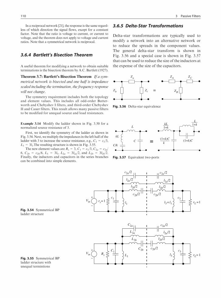
In a reciprocal network [21], the response is the same regard-
less of which direction the signal flows, except for a constant
factor. Note that the ratio is voltage to current, or current tovoltage, and the theorem does not apply to voltage and current
ratios. Note that a symmetrical network is reciprocal.
3.6.4 Bartlett’s Bisection Theorem
A useful theorem for modifying a network to obtain suitable
terminations is the bisection theorem by A.C. Bartlett (1927).
Theorem 3.7: Bartlett’s Bisection Theorem If a sym-
metrical network is bisected and one half is impedance
scaled including the termination, the frequency response
will not change.
The symmetry requirement includes both the topology
and element values. This includes all odd-order Butter-
worth and Chebyshev I filters, and third-order ChebyshevII and Cauer filters. This result allows many passive filters
to be modified for unequal source and load resistances.
Example 3.14 Modify the ladder shown in Fig. 3.50 for a
normalized source resistance of 3.
First, we identify the symmetry of the ladder as shown in
Fig. 3.54.Next,wemultiply the impedances in the left half of theladder with 3 to increase the source resistance, e.g., C1 = c1/3,
L1 = 3l1.The resulting structure is shown in Fig. 3.55.
The new element values areRs=3, C1= c1/3, C2a= c2a/
6, C2b = c2b/6, L1 = 3l1, L2a = 3l2a/2, and L2b = 3l2b/2.Finally, the inductors and capacitors in the series branches
can be combined into simple elements.
3.6.5 Delta-Star Transformations
Delta-star transformations are typically used to
modify a network into an alternative network or
to reduce the spreads in the component values.
The general delta-star transform is shown in
Fig. 3.56 and a special case is shown in Fig. 3.57
that can be used to reduce the size of the inductors at
the expense of the size of the capacitors.
rs= 1 l3= l1 rL=1
c3Vin l1
l2a /2
c2a /2
c2b/2
l2b/2
c1
c2a /2
l2a/2
l2b/2
c2b /2
Fig. 3.54 Symmetrical BP
ladder structure
Rs l3 rL= 1
c3Vin
L2a
C2a c2a/2
c2b/2
l2a/2
l2b/2
C2b
L2b
C1
L1Fig. 3.55 Symmetrical BP
ladder structure withunequal termintions
(1+k)C=
C/k
L
kL
kL
C
1+k
k(1+k)C
L1+k
Fig. 3.57 Equivalent two-ports
ZA
ZB
ZCZa
Zb Zc =
Fig. 3.56 Delta-star equivalence
110 3 Passive Filters

ZA ¼ ZaZb
ZaþZbþZc
ZB ¼ ZbZc
ZaþZbþZc
ZC ¼ ZaZc
ZaþZbþZc
8
>
>
<
>
>
:
Za ¼ ZAZCþZAZBþZBZC
ZB
Zb ¼ ZAZCþZAZBþZBZC
ZC
Zc ¼ ZAZCþZAZBþZBZC
ZA
8
>
>
<
>
>
:
(3:48)
3.6.6 Norton Transformations
The Norton transformations, shown in Figs. 3.58
and 3.59, are useful in the elimination of redundant
elements or for the modification of element values
[12]. Norton transformations can also be used to
reduce the inductance spread and their quality fac-
tors in narrow-band filters [55]. Moreover, using
several successive network transformations, it is
possible to eliminate any redundant elements and
obtain equal source and load terminations. We
demonstrate the use of Norton transformations by
using two examples.
Note that if n 6¼ 1 in the circuits, then one of the
series impedances will be negative. We will later
show how to make use of this fact.
A transformer, with turns ratio n: 1, can be
removed bymultiplying all impedances on the second-
ary side of a transformer with n2. Hence, inductances
and resistances are multiplied by n2 and the capaci-
tances by 1/n2. A voltage sourceV and current source
I on the secondary side are replaced with a voltage
source nV and current source I/n, respectively.
A transformer, with turns ratio n: 1, can be
inserted by dividing all impedances on the
secondary side of a transformer with n2. Hence,
inductances and resistances are multiplied by 1/n2
and the capacitances by n2.
One caution must be observed here. The compo-
nents must be carefully chosen to withstand the
high voltages that may occur after applying this
transformation.
3.6.7 Impedance Transformations
It is often of interest to modify the impedance level in anetwork, or part of a network, without changing its fre-
quency response. For example, some element values may be
difficult to realize. In other cases, it may be desirable to havea network with impedances of similar magnitudes so that all
voltages and currents are of the same order. This will tend to
improve the signal-to-noise ratio.
Figure 3.60 shows some equivalent one-ports that can beused to modify the size of the impedances. For example, if
Z2 = sL2 is a too large inductor and Z1 and aZ1 are suitable
sized capacitors, e.g., a = 2, in the left one-port, then the
corresponding inductor in the equivalent one-port becomes22L2/(2+1)2 = 4L2/9.
The Norton transformations may also be used to change
the impedance level in a part of the network.
Example 3.15 Consider the bandpass filter shown in
Fig. 3.61, which has been derived from a third-order Cheby-
shev I filter with Amax = 0.1 dB and the normalized element
values LLP1 = LLP3 = 1.0316 and CLP2 = 1.1474, and Rs =RL = 1. The passband edges of the geometric symmetrical
filter are oc1 = 100 Mrad/s and oc2 = 105 Mrad/s.
n : 1Z
Zn Z
n(n–1)=Z
1–n
Fig. 3.58 Norton’s first two-port equivalence
(n –1)Z
n : 1
Z =
n
(1– n)Z
n2
Z
n
Fig. 3.59 Norton’s second two-port equivalence
Z1
aZ1
Z2
=
aZ1
b = a+1
2
a Z12
ba Z2
2
b
b
Fig. 3.60 Equivalent one-ports
RsL1 L3
C2
C3
RLVin
+
V2
_
C1
L2
Fig. 3.61 Sixth-order Butterworth bandpass filter
3.6 Network Transformations 111

The denormalized element values in Table 3.2 yield
L1 ¼ L3 ¼LLP
oc2 oc1
¼ 1:0316
5 106 ¼ 0:20632 mH
C1 ¼ C3 ¼oc2 oc1
o2ILLP
¼ 5 1061:05 1016 1:0316 ¼ 0:4616 nF
(3:49)
and
C2 ¼CLP
oc2 oc1
¼ 1:1474
5 : 106¼ 0:22948mF
L1 ¼ L3 ¼LLP
oc2 oc1
¼ 1:0316
5 : 106¼ 0:20632mF
C1 ¼ C3 ¼oc2 oc1
o2ILLP
¼ 5 : 106
1:05 : 1016 : 1:0316¼ 0:4616 nF:
(3:50)
From Equations(3.49)and(3.50), we find that the element
spread is inversely proportional to the relative bandwidth
squared. Because the relative bandwidth is about 5%, the
element values C2 >> C1 and L2 << L1, making the filterdifficult to realize. The element spread is about 497 for both
the capacitors and inductors.
In order to make the element spread smaller, we insert a
transformer on the left side of the shunt branch with turnsratio n1:1. To compensate for the transformer, we divide all
impedances on the secondary side of the transformer with
n12. The output voltage will beV2/n1. The resulting network is
shown in Fig. 3.62.
In the next step, we use Norton’s first equivalence, wherethe capacitor C1 corresponds to Z in Fig. 3.58, to replace the
transformer. We get the network shown in Fig. 3.63.
In the next step, a second transformer with turns ratio n2:1is inserted to the right of the inductor L2, as shown in
Fig. 3.64, where n3= n1n2.
We again use the first Norton equivalence with capacitor
n32C3 as impedance. Note that the turns ratio in Fig. 3.58 is
now n=1/n2, as the equivalence circuit has been flipped over.
To retain equal the source and load resistor, we select n1n2=1.
The new element values shown in Fig. 3.66 are
C3a ¼ð1 n2Þ
n22n23C3 ¼
ð1 n2Þn22
C3
C3b ¼n23C3
n2¼ C3
n1
C3c ¼ðn2 1Þ
n2n23C3 ¼
ðn2 1Þn2
C3:
The capacitors, n1(n1 l)C1 and C3a will be negative if n1< 1. It is possible to eliminate the effective shunt capacitor,
Cx, entirely by an appropriate choice of n1. The effective
shunt capacitor Cx shown in Fig. 3.65 is
Cx ¼ n1ðn1 1ÞC1 þ n21C2 þ ð1 n2Þn21C3:
RsL1
n12C2 RLVin
+
V2
_
C1
n12
L2
n12
L3
n12n1
2C3n1 : 1
Fig. 3.62 Ladder with
inserted transformer
RsL1
Vin
+
V2
_
n1C1
(1–n1)C1
n1(n1–1)C1
n2 : 1
n12C2 L2
n12
L3
n32n3
2C3
RL
n32
Fig. 3.64 Ladder with a
second transformer inserted
RsL1
Vin
+
V2
_
n1C1
(1– n1)C1
n1(n1–1)C1
n12C2 L2
n12
L3
n12n1
2C3
RL
n12Fig. 3.63 The transformer is
removed by using Norton’s
first equivalence
112 3 Passive Filters

If we make Cx = 0 in order to save one capacitor, thenn1 = 4.00692 103, n2 = 249.568, and the spreads in ele-
ment values will become (n2 l)C3/n1n2C1=248.6, which is
somewhat large. In practice, however, the shunt inductorwill in practice have a parasitic capacitance that may be
absorbed into Cx. If we select, for example, n1 = 0.25 and
n2 = 4, which yields Cx = 14.169 nF, the element spread is
reduced to about 122.8 and 16 for the capacitors and induc-tors, respectively.
3.6.8 Transformations to Absorb
Parasitic Capacitance
One problem with the standard synthesis methods is
that they result in networks, as shown in Fig. 3.67,
that have nodes that are not connected to ground
through a shunt branch. Such high-impedance nodes
are sensitive to a stray capacitance. In order to
remove such sensitive nodes, we may perform one
or several successive Norton transformations.
If the LP filter has finite zeros, as shown in
Fig. 3.67, the corresponding bandpass filter will
have series and shunt branches that contain four
circuit elements. This is not good from a sensitivity
point of view. Therefore, different types of network
transformations should be applied, i.e., Norton
transformations, to obtain a BP filter structure
without high-impedance nodes [26, 95, 100, 137,
146]. The filter shown in Fig. 3.67 is very sensitive
for a stray capacitance, Cstray.
Example 3.16 Consider the bandpass filter shown in
Fig. 3.67, which has only one critical node between the twoparallel resonance circuits in the shunt arm.
First, we place a transformer with turns ratio n : 1 imme-
diately after the second parallel resonance circuit, L2bC2b
and divide all impedances on the right side of the transformer
with n2. Next, we apply Norton’s second equivalence, using
the parallel resonance circuit L2bC2b as impedance, to
obtain the ladder network shown in Fig. 3.68.
RsL1
Vin
Cx
C3aC3c
n1C1
(1–n1)C1 n1(n1–1)C1
C3b
L2
n12
n12C2
L3
n32
RL
n32
Fig. 3.65 The transformer isremoved by using Norton’s
first equivalence
RsL1
Vin
0.25C1
16L20.75C1
0.0.25C3 L3
RLCx 0.75C3
Fig. 3.66 Final structure with less element spread
Vin
Rs
L2
C2
RL
+
_
VoutC1 C3
Vin
rs
l1c1
Cstray
l2b
c2b
c3
l3 rL
+
_
Vout
c2a
l2a
Fig. 3.67 Frequency
transformation of an LPfilter with finite zeros to a BP
filter
3.6 Network Transformations 113

The negative shunt components that result from the trans-
formation are combined in parallel with the positive shunt
inductors and capacitors to obtain realizable component
values
nð1 nÞC2b þ n2C3 ¼ 0 ) n ¼ C2b
C2b C3
(3:51)
or alternatively if we select to eliminate the inductance
L2b
nðn 1ÞL3
n2L2b
nðn 1Þ þL3
n2þ L2bL3
n2L2b þ nðn 1ÞL3
¼ 0 ) n ¼ L3
L2b þ L3
: (3:52)
The value of nmay be chosen so that only one additionalshunt capacitor or inductor is required. In most cases, we will
select to remove an inductor. The two rightmost parallel
resonance circuits can be combined to a single circuit. The
resulting circuit has four inductors and five capacitors. TheNorton transformations will usually not maintain equal
source and termination resistances.
3.6.9 Minimum-Inductor Filters
Inductors that are implemented using magnetic
cores are bulky, heavy, and expensive compared
to the capacitors. In applications where a larger
number of filters shall be manufactured, the num-
ber of components in the filter structure are of
economical concern. In addition, in cases when
the physical space is restricted, it is essential to
minimize the number of components. Hence, it is
desirable to minimize the number of inductors.
In so-called parametric filters, two real zeros
are inserted into the characteristic function in
order to trade off some of the attenuation in the
stopband for a more suitable network structure,
or save an inductance, or to have certain relation-
ship between some of the element values, etc.
These zeros will either cancel a transmission zero
at s = 0 or s = 1.
Definition 3.9 A canonical network realizes an
impedance with a minimum number of circuit
elements.
A transmission zero at s = 0 or s = 1 can be
obtained using only a series (or shunt) capacitor,
but the realization of a finite (nonzero) jo-axis zero
pair, however, requires an inductor. Each pair of
real zeros (realized with a C section) also requires
one tapped inductor.
Theorem 3.8: For LP and HP filters, the minimum
number of inductors equals the number of finite (non-
zero) zero pairs.
Figure 3.69 shows examples of lowpass and highpass
ladders where all inductors are used to realize finite zeros.
For BP filters, the situation is more involved. Band-
pass filters with at least two zeros at both s = 0 ands = 1 can be realized with a minimum-inductor ladder
with N/2 inductors, where N is the order of the filter.
That is, the number of inductors equals the number of
zeros, including those at s = 0 and s = 1. So-calledparametric BP filters require only N/2 1 inductors [29,
123, 124].
Rs
RLC1 n2C3
Vin L1
L2b/n
nC2b
L3
+
_
Vout
C2a
L2a
n(n–1)C2b
L2b(1–n)C2b 1–n
L2b
n(n–1) n2 n2
Fig. 3.68 BP structure thatis less sensitive to parasitics
VinVinFig. 3.69 Examples of
minimum-inductor LP and
HP filters
114 3 Passive Filters

Figure 3.70 shows four additional sections that are useful
for realizing BP filters with a minimum number of inductors.
The two sections to the left realize transmission zeros belowthe passband whereas the two on the right realize transmis-
sion zeros above the passband.
Figure 3.71 shows a Laurent14 zig-zag bandpass filter
with double zeros at both s= 0 and s=1, where network
transformations have been used to obtain a minimumnumber of inductors and a small spread in the element
values [33, 48, 49, 100]. The Norton transformations can
be used to reduce the number of inductors. Note that
sections 1 and 6 realize a transmission zero at s = 0, section
5 realizes a transmission zero at s= 0 and s=1, sections 2
and 4 realize a transmission zero in the upper stopband,
and section 3 realizes transmission zeros in the lowerstopband.
Example 3.17 Consider the network in Fig. 3.72, which
contain, a capacitive loop C1C2C3. The order of thetransfer function is therefore one less than the number of
reactive components and one capacitor can therefore be
eliminated.
Inserting a transformer with turns ratio n : 1 in the cutAA’
and using the first Norton equivalence yields the network
shown in Fig. 3.73. It is possible to eliminate either the
capacitor resonating with L1 or with L2 by inserting thetransformer appropriately. Alternatively, if neither of the
capacitors is eliminated, instead, the output impedance is
modified. To eliminate the capacitors resonating with L1,we select C1 þ ð1 nÞC2 ¼ 0: That is, n ¼ ðC2 þ C1Þ=C2:
Alternatively, we can eliminate the capacitors resonatingwith L2 by selecting
Fig. 3.70 BP sections for realization of finite transmission
zeros
Vin Vout
_
+
1 2 3 4 5 6
Fig. 3.71 Laurent zig-zagBP filter with minimum
number of inductors
Vin
A
A’
RL
Rs
C1
C2
C3
L 1 L 3
Fig. 3.72 Ladder structure with a capacitive loop
Vin
Rs
C1
nC2
L 1
(1–n)C2n2C3n(n–1)C2
L 3
n2
RL
n2Fig. 3.73 The transformer
inserted in the cur A-A’ is
removed by using Norton’s
first equivalence
14Torben Laurent, Royal Institute of Technology, Sweden.
3.6 Network Transformations 115

nðn 1ÞC2 þ n2
C3¼ 0, which yields
n ¼ C2=ðC2 þ C3Þ51:
The load resistor RL/n2 will be larger than RL. Note
that if n is small, then the voltages will be large and
the components must be chosen to withstand the
high voltages.
3.7 Lattice Filters
Passive filters can also be implemented using different
types of electromechanical resonators instead of LC
resonance circuits, e.g., piezoelectric crystals. These
types of filters, which will be further discussed in
Section 3.9, often employ so-called lattice structures;
a name suggested by its schematic shown in Fig. 3.74,
with quartz crystals in the branches. The lattice struc-
ture can accommodate such resonators much more
easily than the corresponding ladder structure.
Lattice filters have extremely high sensitivity in
the stopband for errors in the circuit elements, but
this is acceptable because the quartz crystals are
very stable with respect to temperature and ageing.
Several millions of passive filters with crystals or
ceramic circuit elements are nowadays manufac-
tured each month.
In principle, the crystals in the lattice structure
can be replaced withLC circuits, but this is unusable
in practice due to large variations in the element
values. Frequency selective lattice filters with
regular RLC components are therefore not recom-
mended. Moreover, lattice structures are not cano-
nical and require more than a minimal number of
circuit elements.
By redrawing the lattice section, according to
Fig. 3.75, it becomes evident that it in fact has the
same structure as a measurement bridge. Using a
sinusoidal voltage source, the output voltage becomes
zero when the bridge is balanced, i.e., when Za/Zc =
Zb/Zd. Knowing three of the impedances, the fourth
can be determined with very high accuracy at that
frequency. The four impedances are usually pure reac-
tances when the bridge is used as a filter.
When the bridge is balanced, i.e., at a frequency
that corresponds to the transmission zero, the out-
put signal isVout=0.A small variation of any of the
reactances will make Vout nonzero. Hence, the ele-
ment sensitivity in the stopband is very large.
The normalized transfer function of the lattice
filter in Fig. 3.75 is
HðsÞ ¼2Vout
Vin
¼ RLðZbZc ZaZdÞZ1RL þ ðZ2 þ Z3ÞRsRL þ RsZ2Z3 þ Z3ZaZb þ Z2ZcZd
(3:53)
where Z1 ¼ Za þ Zcð Þ Zb þ Zdð Þ;Z2 ¼ Za þ Zb;
and Z3 ¼ Zc þ Zd.
The lattice structure contrary to ladder struc-
tures can realize zeros in the right half of the
s-plane. This is useful for realizing allpass filters.
Moreover, one of the best digital filter structures,
lattice wave digital filters, is derived from analog
lattice structures [135]. In fact, lattice structures are
both of practical and theoretical interest in spite of
their very high stopband sensitivity.
Vin
Rs Za
Zc
Zd
Zb
+
_
VoutRL
Fig. 3.74 Lattice structure
Vin
Rs
Za
Zc Zd
Zb
Vout
RL
+ _
Fig. 3.75 Lattice filter
116 3 Passive Filters

3.7.1 Symmetrical Lattice Structures
Consider the symmetrical lattice filter shown in
Fig. 3.76, where Za = Zd, Zb = Zc, and Rs = RL
= R. Equation (3.53) simplifies for the symmetrical
lattice to
HðsÞ ¼ 2Vout
Vin
¼ RðZb ZaÞðZa þ RÞðZb þ RÞ
¼ 1
2
Zb R
Zb þ R Za R
Za þ R
(3:54)
or
HðsÞ ¼ R1
Rþ Za
1
Rþ Zb
: (3:55)
The reflection functions are
r1ðsÞ ¼ r2ðsÞ ¼1
2
Zb R
Zb þ Rþ Za R
Za þ R
: (3:56)
IfZa andZb are pure reactances, the two terms in
Equation (3.54) become allpass functions. The
impedance Za and Zb can, in principle, be deter-
mined by performing a partial fraction expansion
of transfer function and assigning the appropriate
terms toZa andZb. There is usually only one assign-
ment among the terms that leads to lattice reac-
tances with positive element values.
It can be shown that lattice filters only can realize
odd lowpass and highpass filters and even-order
bandpass filters with zeros at both s = 0 and s =1.
Another disadvantage of the symmetric lattice
structure, besides the very high sensitivity, is the
large number of components required, i.e., twice
the order of the filter.
3.7.2 Synthesis of Lattice Reactances
In this section, we demonstrate by the means of an examplehow the lattice reactances of a symmetric lattice can be
derived.
The lattice reactances can be computed with the following
scheme.
. Find all the transmission zeros and the stopband edge os.
. Compute the characteristic function, whichmust be an odd
function of o.. Form a polynomial X(s) by adding the numerator polyno-
mial, multiplied by e, and denominator polynomial, p(s), of
the characteristic function. The roots of p(s) are the trans-
mission zeros.. Compute the roots of the polynomial X(s) and assign the
roots in the left-half s-plane to h(s) (Hurwitz) and the
roots in the right-half s-plane to ah(s) (anti-Hurwitz).That is, X(s) = h(s) ah(s). A useful program for this step
is hurwitz.. Compute the two lattice reactances, see Theorem 3.10,
if p(s) is even Za ¼ RahoðsÞaheðsÞ
Zb ¼ RheðsÞhoðsÞ
and
if p(s) is odd Za ¼ RahoðsÞaheðsÞ
Zb ¼ RhoðsÞheðsÞ
:
The subscripts e and o indicate polynomials formed by
deleting the odd and even terms of the polynomial, e.g., h(s)
= a s3+ b s2+ c s+d yields ho(s) = a s3+ c s and he(s) = b
s2+ d.
The realization of Za and Zb, can be done by any of the
structures discussed in Section 3.7.7.
Apart from a phase shift with p, lattices with any of thereactance pairs (Za, Zb), (Zb, Za), (R
2/Za, R2/Zb), or (R
2/Zb,
R2/Za) have the same transfer function.
Example 3.18 Determine the lattice reactances for the third-
order Cauer filter C031511 when the passband edge is
oc = 1 rad/s.
Synthesizing the filter, we find that the stopband edge isos = 5.2408 rad/s, Amax = 0.0988324 dB, Amin = 50.625 dB,
and e= 0.1517165. The filter has two transmission zeros at s
= j 6.04657 rad/s and one at s = 1. The characteristic
function is, see Equation (2.49), is
CðsÞ ¼ eRN
s
oc
;L
¼ 21:68806sðs2 þ 0:7512366Þs2 þ 36:561032
:
We form the polynomial X(s) =21.68806 s(s2+0.7512366) + (s2+36.56103) and solve for
its roots
Vin
R
ZaZb
Vout
R
+ _
Za
Zb
Fig. 3.76 Symmetrical lattice filter
3.7 Lattice Filters 117

XðsÞ ¼ 21:68806ðs 0:474289þ j1:212363Þðs 0:474289 j1:212363Þðsþ 0:994686Þ ¼
¼ 21:68806ðs2 0:948578sþ 1:694774Þðsþ 0:994686Þ:
We assign the root in the left half plane to h(s),
i.e., h(s) = s+0.994686, and the remaining to ah(s),
i.e., ah(s) = s20.948578 s+1.694774. Because p(s) is
odd, we get
Za ¼ RahoðsÞaheðsÞ
¼ R0:948578
s2 þ 1:694774
¼ RsL
1þ s2LC:
Hence, a normalized inductor L = 0.988578 in parallel
with a capacitorC=1.7866.R is a factor that determines the
impedance level, i.e., if R = 1 O then L = 0.988578 H
Zb ¼ RhoðsÞheðsÞ
R0:994686
s:
That is, a capacitor C = 1.00534.The computations above have, of course, been carried out
with higher precision than shown.
3.7.3 Element Sensitivity
A major problem of lattice structures is that trans-
mission zeros are realized through a balancing of
the branches, i.e., by making Za = Zb at each zero
frequency. Furthermore, the impedancesmust track
at all frequencies, which requires a large number of
low-tolerance components, making the lattice struc-
ture expensive.
Methods to realize transmission zeros, which are
based on the principle that two currents are summed
in a circuit node, or the difference in voltage
between two nodes, as in the lattice structure, are
very sensitive for errors in the element values and
should therefore be avoided.
The high element sensitivity in the stopband
makes, in practice, the lattice structure with
coils and capacitors unusable for frequency
selective filters. However, lattice structures
with crystals in the bridge arms are useable.
This works well despite the high element sensi-
tivity in the stopband because the crystals are
highly stable and the variations in the element
values are very small.
The element sensitivity in the passband is, how-
ever, small if the lattice section is designed accord-
ing to the insertion loss method.
3.7.4 Bartlett and Brune’s Theorem
Lattice filters are related to symmetrical ladder fil-
ters. A symmetrical ladder filter has always an
equivalent lattice structure having equal transfer
function and the same input impedance. However,
a lattice structure does not always have a symme-
trical ladder counterpart with positive elements.
Theorem 3.9: Bartlett and Brune’s Theorem A sym-
metrical LC network corresponds to a lattice filter
with the impedances Za and Zb, which can be found by
the following procedure:
1. Cut the ladder network along its line of symmetry
into two identical parts.
2. Short-circuit all nodes that lie on the line of sym-
metry. The input impedance to this network is Za.
3. The input impedance of the network (one of the
parts) is Zb.
Figure 3.37 show some equivalent networks
derived by using Bartlett and Brune’s theorem.
According to Bartlett and Brune’s theorem, a sym-
metrical LC ladder network corresponds to a lattice
filter, but the opposite is not always true. Hence, not
all minimum-phase transfer functions can be rea-
lized by a lattice filter. For example, only lowpass
(highpass) filters of odd order and with at least one
zero at s ¼ 1ðs ¼ 0Þ are realizable.
Example 3.19 A symmetrical ladder network is shown in
Fig. 3.78 with L1 = L5 and C2 = C4. Derive the reactances
in the corresponding lattice network.
118 3 Passive Filters

First, we partition the symmetrical network into two
identical parts along the line of symmetry. The inductor L3
is split into two inductors in series, each with the value L3/2.
The reactance Za equals the input impedance when the nodes
at the line of symmetry are short-circuited. The reactance Zb
equals the input impedance to the remaining part of the net-work when the nodes are not short-circuited. In this case, the
inductor L3/2 is superfluous.
Note that the order of the impedances Za and Zb willalways be different.
3.7.5 Bridged-T Networks
A lattice filter can be realized in an equivalent form
with the bridged-T network shown in Fig. 3.79. The
bridged-T network has the advantage that the
source and load have a common ground.
The lattice impedances corresponding to the
impedances in a symmetrical bridged-T network,
i.e., ZB = ZC and Rs = RL = R, is directly obtain
by using Bartlett and Brune’s theorem.
We get
Za ¼ZA
2ZB
ZA
2þ ZB
¼ ZAZB
ZA þ 2ZB
Zb ¼ ZB þ 2ZD:
8
>
>
>
<
>
>
>
:
(3:57)
An unabridged network is obtained by letting
ZA ! 1. We get
ZB ¼ ZC ¼ Za
ZD ¼ Zb Za
2:
(
(3:58)
3.7.6 Half-Lattices
The number of circuit elements can be reduced by
using one of the equivalent unbalanced circuits that
are shown in Fig. 3.80. These circuits, called (incor-
rectly) half-lattices, trade half of the components of
Za
Zb
Za
Zb
Za
Zb
Za
–Za
Zb
–Za
=
Za
Zb
Za
Zb=
–Zb–Zb
Fig 3.77 Equivalentnetworks based on Bartlett
and Brune’s theorem
L1
L1
L3Za
C2Zb
2
L3
2
C2L1L3 L5
C2 C4Z
Fig. 3.78 Example of the
use of Bartlett and Brune’s
theorem
Vin
R
ZA
ZB ZC
ZDR Vout
_
+
Fig. 3.79 Bridged-T network
3.7 Lattice Filters 119

the lattice for an ideal transformer [12]. In addition,
these circuits have higher sensitivity in the stop-
bands than their ladder counterparts.
The chain matrix, see Section 5.4, for the circuits
shown in Fig. 3.80 is
V1
I1
¼
Za þ Zb
Zb Za
2ZaZb
Zb Za
2
Zb Za
Za þ Zb
Zb Za
2
6
6
4
3
7
7
5
V2
I2
: (3:59)
Lattices and half-lattices are used mostly to rea-
lize filters with complex zeros and, especially, filters
using electromechanical resonators.
3.7.7 Reactance One-Ports
To obtain a better realization, it may be advanta-
geous to replace an impedance with an equivalent
one-port. In this section, we discuss four generic
structures for realizing (lossless) reactances and
some often used special cases.
Let F(s) denote a reactance, then F(s) is an
odd positive-real function with the following pro-
perties [124]:
F(s) is an odd function, i.e., F(s) = F(s), with
real coefficients
F(s) ! K/s or Ks when s ! 1 F(s) have only simple poles on the jo-axis with
real and positive residues
The poles and zeros are alternating on the jo-axis
ReF(s) = 0.
Theorem 3.10: The ratio of the even and odd, or odd
and even, parts of a Hurwitz polynomial is an impe-
dance function.
Theorem 3.11: The minimum number of reactances
necessary to realize a lossless impedance or admit-
tance is equal to its degree.
3.7.7.1 Foster I and II
The Foster I realization of an arbitrary reactance
function X(s) is obtained by a partial fraction expan-
sion of the impedance, which can be performed by
the function PART_FRACT_ EXPANSION,
XðsÞ ¼ L1sþ 1
C0sþX
N
i¼1
1
Ci
s
s2 þ o2i
(3:60)
The Foster I structure [23] is shown in Fig. 3.81
where LiCio2i ¼ 1.
The Foster II realization of an arbitrary reac-
tance function X(s) is obtained by instead expand-
ing 1/X(s)
YðsÞ ¼ C1sþ 1
L0sþX
N
i¼1
1
Li
s
s2 þ o2i
: (3:61)
The Foster II realization is shown in Fig. 3.82
where LiCio2i ¼ 1.
Two common special cases of a Foster II circuit
that may occur in the LP-BP transformation and its
corresponding equivalent Foster I circuit are shown
in Figs. 3.83 and 3.84.
1:–1
Za
Zb
2
2
1
1
2Za
2Zb
1:–1
Zb2
2Za
= =
Fig. 3.80 Examples of two-port equivalents of a
symmetric lattice
L∞
L1 L2 LN
C0C1 C2 CΝ
Fig. 3.81 Foster I structure
120 3 Passive Filters

3.7.7.2 Cauer I and II
The Cauer I realization [23] is obtained by a con-
tinued fraction expansion of X(s) around s = 1according to
XðsÞ ¼ L11sþ1
C12sþ1
L13sþ1
C14sþ . . .
(3:62)
The Cauer I realization is shown in Fig. 3.85.
Note that the reactance can either be terminated
with an open-circuit or short-circuit for an even-
order and odd-order reactance, respectively. For
reactances with order 3, the Cauer I and Foster
I structures become identical.
The Cauer II realization is obtained by expand-
ing X(s) around s = 0 according to
XðsÞ ¼ 1
C01sþ 1
1
L02sþ 1
1
C03sþ 1
1
L04sþ . . .
(3:63)
The Cauer II realization is shown in Fig. 3.86.
Note that the reactance can either be terminated
with an open-circuit or short-circuit. For reactances
with order 3, the Cauer II and Foster II structures
become identical.
Deffinition 3.10 A canonical reactance network has
a minimum number of inductors and capacitors.
Both the Foster and Cauer networks are canoni-
cal and require aminimumnumber of inductors and
capacitors. Non-canonical networks use more than
the minimum number of components to realize an
impedance function.
3.8 Allpass Filters
Here we will only discuss lattice structures of allpass
type, which are realized with a symmetrical lattice
section, i.e., withRs=RL,Za=Zd andZb=Zc, or
the corresponding equivalent bridged-T network.
The latter network has the advantage of only requir-
ing two impedances and a tapped inductor whereas
the lattice structure requires four impedances.
Furthermore, the bridged-T network has common
ground between input and output.
To equalize the group delay of a minimum-phase
filter,Hm(s), i.e., a filter that does not have any zeros in
the right-half s-plane, we use an allpass filter in
C∞L0
C1 C2 CN
L1 L2 LN
Fig. 3.82 Foster II structure
=
Fig. 3.84 Equivalent Foster I and II structures
=
Fig. 3.83 Equivalent Foster I and II structures
L∞1 L∞3 L∞5
C∞2 C∞4 C∞6
Fig. 3.85 Cauer I structure
C01 C03 C05
L02 L04 L06
Fig. 3.86 Cauer II structure
3.8 Allpass Filters 121

cascade withHm(s). In fact, a ladder network can only
realize transfer functions of minimum-phase type.
An allpass filter, however, has all zeros in the right-
half s-plane is are therefore a maximum-phase filter.
3.8.1 Constant-R Lattice Filters
If we choose
ZaZb ¼ R2 (3:64)
where Za and Zb are pure reactances, an allpass
filter with interesting properties is obtained. The
transfer function is
HðsÞ ¼ Zb R
Zb þ R: (3:65)
Input and output impedances in such a lattice
structure are Zi = Zo= R. Therefore, the Sections
are called constant-R lattice sections (Otto Zobel).
Note that the multiplexers discussed in Section 3.5.4
also have constant input impedance, Zi = R, but
they are not of allpass type.
The transfer functions for the two allpass filters
shown in Figs. 3.88 and 3.89 are given by Equations
(3.64) and (3.65).
We get
HAP1 ¼ s R=L
sþ R=L(3:66)
where C = L/R2 and
HAP2 ¼s2 s
RC2
þ 1
L2C2
s2 þ s
RC2
þ 1
L2C2
(3:67)
where C1 = L2/R2 and L1 = C2R
2.
3.8.2 Constant-R Bridged-T Sections
In order to reduce the number of components com-
pared to the lattice structure, it is common to instead
use bridged-T networks. Another advantage is that
they have a common ground. A constant-R bridged-
T network is obtained using the network shown in
Fig. 3.79 with ZB = ZC = R and ZA = ZD = R2.
The transfer functions for the networks shown in
Fig. 3.90 are given by Equations (3.66) and (3.67),
respectively. The first-order section, however,
requires a negative inductor that can, according to
Fig. 3.28, be realized by a tapped coil.
3.8.3 Constant-R Right-L and Left-L
Sections
The two networks shown in Fig. 3.91 are also con-
stant-R networks, when terminated with a resistor
R, and if Equation (3.64) holds. The transfer func-
tions are
Vin
R
Za
Zb
Za
Zb
+
_
VoutR
Zi = R Zo = R
Fig. 3.87 Constant-R lattice
V1 V2
R L
LC C
_
+
R
Fig.3.88 First-order constant-R lattice
V1
C2
L2
L1 L1
C1 C1
C2
V2
+
_
R
L2
R
Fig.3.89 Second-order constant-R lattice
122 3 Passive Filters

HðsÞ ¼ 1
1þ Za=R(3:68)
Constant-R sections are useful for realizing a
Hilbert filter, which is a three-port where the two
output ports have the same constant magnitude
function, but their phase-difference approximates
908 over a prescribed band of frequencies.
The structure resembles the diplexer shown in
Figure 3.41, but the two branches consist of con-
stant-R sections, i.e., allpass sections.
3.8.4 Equalizing the Group Delay
Theorem 3.12: The group delay of a reciprocal loss-
less two-port is an even nonnegative function of o.
Several sections can be cascaded according to
Fig. 3.92. Because every section has the load resis-
tor, R, we can replace it with a new lattice structure
with the input impedance R, and so on. The lattice
sections will not interact.
Figures 3.88 and 3.89 show two examples of first-
and second-order lattice structures [11, 26, 146] and
the corresponding bridged-T networks are shown in
Fig. 3.90.
Example 3.20 Determine the element values in a third-order
allpass filter built of cascaded bridged-T networks thatequalizes the group delay of the ladder network in
Example 2.4 when Rs = RL = 1000 O.
The poles of the allpass filter were in Example 2.11 deter-
mined to
sp1 = 7.1328393364267 j 6.5766989368398
krad/s
sp2 = 7.0319414698343 j 19.3771121673633krad/s
sp3 = 6.7508088487487 j 32.4760875022130
krad/s.
From Equation (3.67), we obtain the element values in the
lattice structures. We get using 1/RC2 = 2 Resp and 1/
L2C2 = rp2 and R = 1 kO.
R
Za
Zb
RZa
Zb
Fig. 3.91 Left-Land right-Lconstant-R networks
V2
+
_
V1
R 2L
2C R
N = 1
V1
(C2–C1)/2
R
+
_N = 2
2L2
V2
R
2
L1C1 C1
Fig. 3.90 Bridged-T networks
Vin
R
+
_
VoutR
Zin = R Zin = R Zin = R Zin = R
...
Fig. 3.92 Cascaded
constant-R sections
3.8 Allpass Filters 123

Bridged-T L1[mH] L2[mH] C1[nF] C2[nF]
1 70.09831 151.55237 151.5524 70.098312
2 71.10412 33.09767 33.09767 71.10412
3 74.06520 12.27119 12.27119 74.06520
The element values of the LP filter were determined using
CA_LADDER. The resulting equalized LP filter is shown in
Fig. 3.93.
From the lattice structures, the element values can then becomputed in the corresponding bridged-T network. In prac-
tice, bridged-T networks are used because they have fewer
components than lattice structures and they have common
ground between the input and output. Note that the allpasssections can be put in any order at the output, or at the input,
or a combination thereof, as Rs = RL in this case.
If a general synthesis program is available, wemay instead
of using this approach synthesize a ladder with one or severalallpass sections inside the ladder as this often lead to a less
sensitive overall structure.
3.8.5 Attenuation Equalizing
Constant-resistance lattice sections and bridge-T net-
works can also be used to equalize the attenuation; for
example, to reduce the attenuation in a neighborhood
of the passband edge that is deteriorated because of
use of coils with too low Q factors. However, in this
case the sections are not allpass sections.
3.9 Electromechanical Filters
As discussed in Section 3.3, a doubly resistively termi-
nated lossless LC network can be designed to have
optimal sensitivity in the passband. An alternative
approach to implement such passive filters is to
replace the LC resonance circuits with lossless
mechanical resonators. Electromechanical filters that
realize a doubly resistively terminated lossless network
with maximum power transfer have therefore also
optimal sensitivity in the passband. However, electro-
mechanical filters are solely bandpass filters.
In an electromechanical filter, the input signal
carrier (voltage or current) is converted intomechan-
ical form, e.g., vibrations, by means of an input
transducer, as illustrated in Fig. 3.94. Typically, the
signal carrier after the input transducer is a force or
velocity. The actual filtering takes place within the
mechanical structure, which is composed of reso-
nators and coupling elements. Finally, the filtered
signal carrier is then converted back into electrical
form by means of the output transducer.
Electromechanical filters are typically used in
telecommunication systems, for example in carrier
frequency systems and in intermediate frequency
(IF) filters in radio and TV sets as well as in con-
sumer electronics [57, 60, 80].
3.9.1 Mechanical Filters
True mechanical BP filters can be manufactured with the
center frequency in the interval 10 kHz to 10 MHz. Mechan-
ical filters, with constant modulus iron-nickel alloy
Vin
_
+
Vout
Fig. 3.93 LP filter with
equalized group delay
+
_
RL Vout
Rs
Vin
Input
tran
sduce
r
Outp
ut
tran
sduce
r
Res
onat
ors
and
coupli
ng e
lem
ents
Force and Velocity Voltage and
Current
Voltage and
Current
Fig. 3.94 Electromechanical bandpass filter
124 3 Passive Filters

resonators, can be implemented with Q factors up to 10,000,
and with better stability than conventional filters built with
coils, capacitors, and active elements. For example, it ispossible to build a mechanical IF filter with a bandwidth of
500 Hz, centered at 455 kHz, i.e., the relative bandwidth is
only 0.11%. Significant rounding of the passband response,due to losses, is avoided due to the high Q factors of the
resonators. The center frequency shift may be as low as
50 Hz for a 1008C change in temperature.
Figure 3.95 shows the principle for implementation of amechanical filter. The transducer converts a voltage to a force
using a coil with a magnetorestrictive core, which changes its
dimensions proportionally to the magnetic field. The core will
therefore vibrate analogously to the input signal. The vibrationsin the core are then transferred to the resonator structure by
means of thin wires. The wires act as springs when they are less
than one-eighth acoustic wavelength long. The frequencyresponse is determined by the resonance frequencies and the
coupling between the resonators. The resonators can be shaped
in many different ways, i.e., long rods or disks.
The resonators shown in Fig. 3.95 are torodial resonators.Finally, at the output, the vibrations in the last resonator are
connected to another magnetorestrictive core. The changes in
its dimensions produce a magnetic field that generates a
proportional voltage in the output coil.
Frequency selective filters withmechanical circuit elementare characterized by
. Very large Q factors
. Very narrow banded bandpass filters
. Aging and temperature stability
. Low cost
. High reliability
. Cannot be integrated in an IC and have thereforebeen replaced by integrated circuit compatible
technologies.
3.9.1.1 Integrated Microelectromechanical
Filters
MEMS (microelectromechanical systems) is an
emerging technology that uses the same CMOS
processes as for regular integrated circuits to man-
ufacture very small mechanical systems on silicon.
Typical subsystems are switches for antennas, IF
filters, front-end RF filtering, and demodulation in
cellular phones.
The CMOS process that is used has the potential
advantage of mass fabrication of the filters, but they
do not have sufficient geometrical precision. Typi-
cally, the error in the resonator frequency is about
0.5% andmay cause significant passband deviation.
The resonator structure must therefore, for highly
frequency selective filters, be tuned to adjust the
filter characteristics. The tuning involves special
processes for removing or adding material from
the resonators.
Most microelectromechanical filters are imple-
mented using one or several flexural-mode beam
elements on top of the silicon substrate, as shown
in Fig. 3.96. The beam, which is suspended in free
air, is clamped at both ends to the substrate and
connected to electrode 2 at one end. Underneath the
beam is electrode 1. Both the beam and electrodes
are made of conductive materials, such as metal or
doped silicon.
The micromechanical resonator structure, shown
in Fig. 3.96, has two electrical inputs, V1 and V2,
which are applied to the electrode-1 and the beam
through electrode 2, respectively. Hence, a voltage
(V2V1) is applied across the electrode-1-to-beam
gap, generating a force between electrode 1 and the
movable beam. A variation in the voltage (V2V1)
will therefore produce a proportional vibration in the
beam. Several such resonator structures can be elec-
trically or mechanically coupled to implement a
higher order filter. At the output, an electrical signal
can be obtained, as the vibrating beamwill modulate
the electrode-to-beam capacitance.
The clamped-clamped resonators are usable for
frequencies from about 250 kHz to 100 MHz, and
Q factors of up to 10,000 can be obtained. However,
Pins
Transducer Resonators Transducer
Fig. 3.95 Example of a mechanical filter
Electrode 1 Electrode 2
Fig. 3.96 Clamped-clamped beam resonator
3.9 Electromechanical Filters 125

at frequencies over 30 MHz, the mechanical energy
loss to the substrate becomes large and limits the
attainable Q factors. To obtain high Q factors at
high frequencies requires beams with both ends free,
but this requires additional complex mechanical
circuitry.
3.9.2 Crystal Filters
The main difference between a mechanical band-
pass filter and a crystal or ceramic filter is that, in
the case of mechanical filters, both the resonators
and their coupling are mechanical, whereas in crys-
tal and ceramic filters, the resonators are made out
of piezoelectric materials and the coupling is accom-
plished electrically using capacitors and inductors.
Piezoelectricity, which was discovered by the Pierre
Curie and Jacques Curie in the 1880 s, is found in
many crystalline materials, e.g., quartz. One of its
first practical usages was in World War I, when
sonar systems used quartz crystals to generate directed
pulses at audio frequencies to detect submarines.
The piezoelectric effect is stronger in ceramics,
but quartz is still widely used, because it has low
acoustic losses and good temperature stability.
A resonator consists of a freely supported paral-
lel-sided piezoelectric plate with an electrode on
each major face. When a voltage is applied, the
impedance is found to show a sharp resonance due
to the excitation of acoustic waves, reflected many
times between the two faces. Quartz resonators are
used as the controlling element of oscillators used in
clocks, watches, and in electronic equipment, wher-
ever accurate frequency or timing information is
needed.The resonator structure, shown in Fig. 3.94, consists of
piezoelectric crystal or ceramic resonators. The transducers
convert between a voltage to pressure or vice versa. Hence, a
varying input voltage will make the resonator to vibrate
proportionally.Crystal and ceramic filters are also based on doubly resis-
tively terminated reactance networks that are designed for
maximum power transfer, but the conventional resonance
circuits consisting of inductors and capacitors are replacedwithmechanical resonators. Crystal filters are able to provide
narrow bandwidth filtering without excessive loss, tempera-
ture drift, and ageing.
Figure 3.97 shows the symbol for a crystal or ceramicresonator and a corresponding electrical model. The capaci-
tance Cp represents the capacitance of the electrodes.
The equivalent electric circuit contains several (lossy)
series resonance circuits, each representing a particular har-monic mode. The resonator can, for example, oscillate in
parallel resonance mode, i.e., L1Cp, or in series resonance
mode, L1C1. In the first case, the impedance of the resona-
tor becomes large whereas in the series resonance case itbecomes small. For quartz, the series-resonant circuit,
C1L1, has an extremely high Q factor, ranging from about
104 to 106. Hence, the deterioration of the passband edges dueto losses is small.
We may assume that the crystal is operated in the close
neighborhood of one of its resonance frequencies, e.g., f1, and
the influence of the other branches (resonances) areneglected. This is, of course, only valid in a narrow frequency
range around f1. This assumption is only valid in the design
and implementation of very narrow bandpass filters where it
is possible to replace subcircuits in an LC ladder structurewith crystals, or crystal-capacitors. This approach, however,
is restricted to filters with extremely narrow relative band-
widths < 0.1%.Ladder structures with relative bandwidths of 5%, or
more, are not realizable by crystals and capacitors alone,
because of too small capacitance ratios, C1/Cp. It is therefore
better to use a lattice structure, which tends to have highercapacitance ratios than its ladder counterpart does.
In principle, we may realize the whole filter (if it is symme-
trical) by a single lattice, but because of sensitivity reasons, it is
better to use a cascade of simple lattices and ladder sections.Often, the best structure is a cascade of simple lattice sections
with shunt or series capacitors or inductors between the sec-
tions. Lattice structures are very sensitive for circuit elementerrors, but it is still possible to use such structures, as the
crystals are very stable [48, 59].
Figure 3.98 shows a half lattice sectionwith two crystals, a
capacitor, and a transformer. This type of crystal filter is
R1
C1
L1
Cp
ω1
Rn
Cn
Ln
ωn
Fig. 3.97 Symbol for a crystal and corresponding model
Vin
Rs
RL
C1
Fig. 3.98 Example of simple crystal filter
126 3 Passive Filters

often used in the IF part of more expensive receivers. Today,
millions of passive filters with crystals or ceramic circuit
resonators are manufactured annually and used in mostradio and TV receivers.
For filters with relative bandwidths of more than about
10% it is only possible to realize a few selected attenuationpeaks by embedding crystals into an LC ladder structure.
Figure 3.99 shows an example of the implementation of a
simple crystal filter. See [80, 123] for a more detailed discus-
sion of electromechanical filters and their design.
Characteristic of crystal filters, which always are verynarrow band BP filters, are that passbands of only a couple
of hundred Hz and with center frequencies of tens of MHz
can be implemented. Sometimes the term form factor is used,
which is defined as the bandwidth at the attenuation 60 dBdivided with the bandwidth at the attenuation 6 dB. The form
factor can be less than 1.5. Crystals can bemanufactured with
center frequencies in the range 1.5400 MHz and with rela-
tive bandwidths in the range 0.004–0.05%. Crystal filtershave small losses and good signal dynamic.
3.9.3 Ceramic Filters
Ceramic filters are based on piezoelectric ceramics,
and the design principles resemble those of crystal
filters [123]. Piezoelectric ceramic resonators can
only be used to realize narrow bandpass filters.
Ceramic resonators have lower Q factors compared
to crystal resonators. Typically, Q factors is of the
order a few thousand. Ceramic filters are also used
in radio and TV sets. A common application is IF
filters with, e.g., 10.7 MHz center frequency. The
dimension of crystal and ceramic filters is small. For
example, a ceramic filter, from MurataTM, which is
intended for Bluetooth applications, consisting of
three resonators, has been implemented in a small
package (2 4.5 4 mm). The filter is a bandpass
filter with passband 24002500 MHz with a
variation of 2.7–3 dB in the passband and attenuat-
ing at least 25 dB at 1950MHz, 16 dB at 2200MHz,
and 9.5 dB at 2700 MHz.
3.9.4 Surface Acoustic Wave Filters
The first surface acoustic wave filters (SAWs)
appeared in the mid-1960’s. A SAW device operates
by converting electrical energy, through an interdi-
gital transducer (IDT), into a surface acoustic wave
on a piezoelectric crystal plate (substrate). The out-
put is typically obtained through a second IDT, as
illustrated in Fig. 3.100, but there are resonator
structures with a single port. The transducer,
which consists of an array of metallic electrodes on
the surface of the substrate, determines the fre-
quency response. Another basic SAW component
is the reflector, which consists of periodic arrays of
either metal strips or grooves.
By combining IDTs and reflectors, SAW resonators and
resonator filters can be implemented for frequencies in therange from about 10 MHz up at a few GHz. The Q factor of
SAW resonators is relatively low, typically between 6000 and
12,000. SAW filters can be designed to have linear phase,contrary to analog filters realized with lumped elements.
SAWs are relatively easy to manufacture because they
require only one or two photoresist and metal deposition
steps.Surface acoustic wave filters (SAW filter) are commonly
used in radio, TV sets, video players, WLAN, and cellular
phones [122, 123]. Diplexers for WCDMA are also imple-
mented in SAW technologies. Surface acoustic wave filtersare based on a special type of wave propagation mode of
acoustic waves, so-called Rayleigh waves15, on the surface of
a piezoelectric material. However, there exist similar devicesthat use different types of wave propagation modes. Usually
quartz, lithium tantalate (LiTaO3), or lithium niobate are
used. Surface acoustic wave filters for cellular phones are
Pins
Electrode
Support
Package
Isolator
Quartz Crystal
Fig. 3.99 Example of simple crystal
Substrate
Inp
ut
Ou
tpu
t
Fig.3.100 SAW filter
15Lord Rayleigh,1885.
3.9 Electromechanical Filters 127

small, a few mm2, but they cannot easily be implemented on
top of an integrated circuit.
Surface acoustic wave filters can be manufactured withvery narrow transition bands. In principle, surface acoustic
wave filters can be designed with linear phase, but in practice,
a small phase distortion is obtained. Typically, 1o to 5o,and the passband has a constant attenuation of a few dB.
Stopband attenuations of 40 to 60 dB can be obtained. Pass-
band ripples as low as 0.3 dB is achievable. Usable
frequency ranges are 10MHz 4 GHz and the relative band-widths are in the range 0.1% to 10%. For example, a SAW
filter for GSM with Amax = 2 dB has a bandwidth of 25 kHz
that is centered at 902.5 MHz (transmitter) and 947.5 MHz
(receiver). The weight is only 0.15 g and with the dimensions3.8 3.8 1.6 mm.
Today, several hundred millions of surface acoustic wave
filters are manufactured annually. SAW filters are used inmost cellular phone and TV sets. Currently, extensive
research is ongoing with aim at replacing SAW filters with
other filtering techniques, which can be integrated in a reg-
ular integrated circuit, or radio architectures that alleviatethe filtering requirements.
Figure 3.101 shows a simplified block diagram for the
receiver in a GSM phone with two down converter stages.
The first stage is followed by a surface acoustic wave filter(SAW) of bandpass type with a center frequency of approxi-
mately 85 MHz and a bandwidth of approximately 6 MHz
while the second stage has a typical center frequency in the
range 10–20 MHz. This transceiver architecture is expensive,and simpler and less expensive alternative exists.
3.9.5 Bulk Acoustic Wave Filters
In the past decade, many other types of acoustic
wave filters have been developed in order to achieve
ultralow power consumption and greater integra-
tion levels, particularly in RF transceivers. For
example, devices operating with different types of
waves: bulk acoustic waves, BleusteinGulyaev
waves, Lamb waves, and Love waves. Bulk acoustic
wave devices are much smaller than their electro-
magnetic distributed element counterparts are, as
acoustic waves propagate about four to five orders
of magnitude slower than electromagnetic waves.
BAW resonators and filters are suitable for wire-
less communication systems, as they can operate in
the range 2–20 GHz with very high Q factors, and
have large power capability and low volume.
Furthermore, BAW devices have an advantage
over technologies such as ceramic or SAW filters,
as they can be fabricated on top of integrated cir-
cuits. Such a co-integration reduces even further the
size and the cost of high-performance RF front-
ends. Bulk acoustic wave (BAW) and film bulk
acoustic resonator (FBAR) filters are determined
to replace conventional RF filters in cellular phones
as they have now evolved in performance beyond
SAW filters and can be manufactured at a very low
cost using standard IC process steps.
Thin film bulk acoustic wave resonators
(FBARs) convert electrical energy into an acoustic
wave, but unlike SAW devices, the wave is directed
into the bulk. The primary mode is a longitudinal
wave, whereas a SAW employs either a Rayleigh
wave or a surface-skimming wave.
There are two main types of resonators, air gap
and solidly mounted resonators (SMRs). The first
type, which is illustrated in Fig. 3.102, consists of a
piezoelectric membrane, sandwiched between two
electrodes, that is supported at the edges, but free
from the substrate in the resonator region. The elec-
trodes can be directly connected to the top levelmetal
interconnect of the integrated circuit that is used as
substrate. The most commonly used piezoelectric
material for BAWdevices is aluminumnitride (AlN).
An alternative mode of operation is to use Lamb
waves (1988). A Lambwave resonator (LWR) is also
composed of a thin piezoelectric layer sandwiched
between two thin electrodes on top of themembrane.
The piezoelectric layer is small compared to the
wavelength. However, whereas the FBAR operates
LNA
HBP(s)
LO1
SAW
LO2
SAW
Transmitter
Fig. 3.101 Simplified block diagram for the receiver of a
GSM phone
Top levelmetal
Substrate – Integrated circuit
Membrane
Electrode
Pizoelectric layer
Air cavity
Fig. 3.102 Suspended membrane BAW resonator
128 3 Passive Filters

using vertical wave propagation, the LWR employs
lateral wave propagation. Lamb wave resonators
used in IF filters offers high quality factors (>1000)
and on top of IC integration.
The second type of resonator also consists of
such a membrane, but the air gap is replaced with
a sequence of quarter-wavelength thick layers with
alternating high and low acoustic impedances, as
illustrated in Fig. 3.103
The acoustic wave that is generated in the reso-
nator has a component that propagates vertically
downwards. Multiple reflections from these layers
form a standing wave that approximates a free air
surface reflection. Hence, acoustically, the mem-
brane appears to be suspended in free air. In addi-
tion, in this case, the electrodes can be directly con-
nected to the top-level metal interconnect of the
integrated circuit that is used as substrate.
The resonance frequency of a BAW resonator is
determined by the thickness of the piezoelectric layer
and the neighboring layers. In an LWR, the reso-
nance appears when the length of the piezoelectric
layerL= l/2. The BWRandLWRhave a resonance
and an anti-resonance and can be used as resonators
in both ladder and lattice structures as well as in
oscillators. However, the special design techniques
that are required to effectively use only one of the
resonances are beyond the scope of this book.
The required tolerance for the resonance fre-
quency is around 0.1% for filters used in typical
communication systems, and the tolerance
requirements are in the same range for the piezo-
electric layer and the electrodes. These stringent
thickness tolerances cannot be met by standard
tools for IC processes. Hence, there are still pro-
blems regarding thickness tolerances to be solved.
Thin film BAW filters that are based on AlN
or ZnO have high Q factors and can handle high
signal power and operate at frequencies in the range
2–16 GHz where they are expected to replace SAW
filters. In addition, both FBAR and SMR based
filters and oscillators have small sizes and their
implementation is compatible with standard IC
processes. The main advantages of BAW over the
SAW filters are intrinsically low insertion loss, the
smaller temperature drift, and the possibility to be
implemented on top of IC devices.
3.10 Problems
3.1 A coil has the inductance 1 mH andQ= 500 at
10 kHz. Determine the size of the equivalent
series resistor in the simple model.
3.2 Determine the transfer function of a doubly
resistively terminated LC network when the
LC part consists of a capacitor and inductor in
parallel in series branch.
3.3 Show that the ratio of dissipated power, P2, and
maximally transferred power, P2max, in a dou-
bly resistively terminated LC ladder network is
proportional to |H(jo)|2.
3.4 Prove the maximum power transfer theorem.
3.5 Compute the output signal for a doubly resistively
terminated LC ladder network with Rs = RL
that realizes the transfer function C055030 when
the input signal isVin(t)=2 sin(ot) foro=0and
o=oc. Also compute themaximal output power
when the filter is terminated with equal resistors.
3.6 a) A filter realized with a T network with Rs =
RL = 600 O, L1 = 600 mH, C2 = 3.3 mF,
and L3 = 600 mH has the desired frequency
response. Determine the element values if
the load resistor is changed to 1 kO.
b) The passband edge, 1 krad/s, but we need a
passband edge of 3MHz. Determine the new
element values.
3.7 A lowpass RC section has been normalized
so that the attenuation is 3.0102 dB at oc = 1,
Electrode
Substrate – Integrated circuit
Low impedance layer
Electrode
Pizoelectric layer
Low impedance layer
Low impedance layer
High impedance layer
High impedance layer
Fig. 3.103 Solidly mounted BAW resonator
3.10 Problems 129

R = 1, and C = 1. Denormalize the section so
that the 3 dB edge occurs at fc = 1.2 kHz and
R = 10 kO.
3.8 Determine suitable element values using the
MATLAB program for ladder network of p
type with Rs = RL = 50 O that meets
the following specification: Amax = 0.01 dB,
oc = 200 Mrad/s, os = 700 Mrad/s, and
Amin = 50 dB. The filter shall be of type
a) Butterworth filter
b) Chebyshev I filter
c) Chebyshev II filter
d) Cauer filter
3.9 Determine suitable element values for an LC
ladder network of Butterworth type that meets
the requirements: Amax = 0.1 dB, oc =
100 krad/s,os=600 krad/s, andAmin=60 dB.
a) T network with Rs = RL = 50 O
b) p network with Rs = RL = 50 O
c) p network with Rs = 600 O and RL = 300 O
3.10 Determine suitable element values for an
LC ladder network of Chebyshev I type
that meets the requirements: Amax = 0.5
dB, fc = 500 kHz, fs = 2500 kHz, and
Amin = 30 dB.
a) T network with Rs = RL = 50 O
b) p network with Rs = RL = 50 O
3.11 Synthesize a lowpass LC ladder network with
a ripple less than Amax = 0.5 dB in the pass-
band and with fc = 22 MHz, fs = 33 MHz,
and Amin = 24 dB. Use a T ladder with Rs =
RL = 50 O.
3.12 Determine suitable element values in a T lad-
der with Rs = RL= 50 O that realizes a
fifth-order Cauer filter with Amax = 0.1 dB,
oc = 100 Mrad/s, os = 215 Mrad/s, and
Amin = 40 dB.
3.13 Synthesize a doubly resistively terminated
ladder network of p type that realizes the
filter C031534. Use equal termination resis-
tances of 50 O. The passband edge is 800p
Mrad/s.
3.14 Derive the expressions for the LP-HP trans-
formation of the specification, resistors, induc-
tors, and capacitor.
3.15 Realize an LC ladder of Butterworth type with
minimumorder thatmeets the specification:Amax
= 0.5 dB, Amin = 25 dB, fc = 15 kHz, and fs =
6 kHz. Use a p ladder. Rs = RL = 50 O.
3.16 Realize an LC ladder that meets the
same specification as in Problem 5.2 but of
Chebyshev I type.
3.17 Realize a doubly resistively terminated LC
ladder of Cauer type that meets the require-
ment: Amax =0.09883 dB, Amin =28 dB, fc =
7.5 MHz, and fs = 2 MHz. Select Rs = RL =
50 O.
3.18 a) Determine the element values in the
diplexer, shown in Fig. 3.104, with a Butter-
worth frequency response that can be used
as branching filter in an audio system with
8O speaker elements. The crossover fre-
quency should be 2.5 kHz.
b) Determine the input impedance to the
diplexer. Discuss any advantages with
this particular choice of input impedance.
c) Suggest how the branching filter can be
modified to include a subwoofer as well.
3.19 Derive the expressions for the LP-BP transfor-
mation of the specification, resistors, induc-
tors, and capacitors.
3.20 Determine the element values in a Butterworth
ladder structure that meets the requirement:
r = 15%, i.e., Amax = 0.09883 dB, Amin = 40
dB, oc1 = 40 Mrad/s, oc2 = 90 Mrad/s,
os1 = s, and/s, and os2 = 3/s. Use a p ladder
network with Rs = RL = 100 O. Determine the
Vin
L1 L3
C2 RL
+
_
VLP
+
_
VHPRL
C3
L2
C1
Woofe
rT
wee
ter
Fig. 3.104 Diplexer
130 3 Passive Filters

number of zeros for s = 0 and s = 1 and the
number of poles for the BP filter.
3.21 Realize a minimal order Chebyshev I LC
ladder that meets the following specification:
r=15%, i.e., Amax = 0.09883 dB, Amin = 40
dB,oc1=12p krad/s,oc2=18p krad/s,os1=8p
krad/s, and os2=24p krad/s. Use a T ladder
with Rs = RL = 500 O.
3.22 Synthesize a Chebyshev I ladder filter of
minimal order that meets the requirement:
r = 15%, i.e., Amax = 0.09883, Amin = 22
dB, oc1=10p krad/s, oc2=20p krad/s,
os1=2p krad/s, and os2=40p krad/s. Use a p
ladder with Rs = 500 O and RL = 1 kO.
3.23 Realize a Chebyshev I LC ladder filter that
meets the requirement: r = 15%, i.e., Amax
= 0.09883 dB, Amin = 22 dB, oc1=1000p
krad/s, oc2=2200p krad/s, os1=500p krad/s,
and os2=4200p krad/s. Use a T ladder with
Rs = RL = 600 O.
3.24 Determine the element values in a Cauer lad-
der that meets the requirement: r= 15%, i.e.,
Amax = 0.09883 dB, Amin = 40 dB, oc1=40
Mrad/s, oc2=90 Mrad/s, os1=24 Mrad/s,
and os2=150 Mrad/s. The ladder network
shall be of p type and double resistively termi-
nated with Rs = RL = 100 O.
3.25 Derive the expressions for the LP-BS transfor-
mation of the attenuation specification, resis-
tors, inductors, and capacitors.
3.26 Determine the element values in double resistively
terminatedpRs=RL=100O. The filter shall be
of Chebyshev I type and meet the specification:
oc1=2p 49.5 rad/s oc2=2p 50.5 rad/s
os1=2p 48.5 rad/s os2=2p 51.5 rad/s
Amax1=Amax2=2dB, Amin=35 dB
3.27 Derive the dual network and its element values
to a p ladder that realizes the Cauer filter
C051523.
3.28 Find the dual of the network in Fig. 3.45.
3.29 Derive the transfer function for a symmetrical
lattice structure and determine necessary con-
straints on Za, Zb, and R if the network shall
realize the transfer function in Equation (3.65)
that corresponds to a constant-R lattice section.
3.30 Show how the group delay of a doubly
resistively terminated ladder network can be
equalized using constant-R lattice sections.
Determine also suitable element values for an
allpass filter that realizes the poles: sp0 = 1
and sp1,2 = 3 j 4.
3.31 Show the input impedance of the bridged-T
network in Fig. 3.105 isZin=R and determine
the transfer function when ZaZb = R2.
3.32 Find the lattice equivalent to the bridged-T
network shown in Fig. 3.106.
3.33 Verify that the bridged-T and the right-L and left-
L networks are constant-R networks when termi-
nated with a resistor R and if ZaZb = R2. Verify
also that the voltage transfer functions are.
3.34 Validate Equations (3.51) and(3.52) and
derive the resulting element values if one
inductor is eliminated.
3.35 a) Where in the s-plane can the following
structures realize poles and zeros.
b) Doubly resistively terminated ladder network.
c) Doubly resistively terminated lattice network.
d) Why is a doubly resistively terminated lad-
der preferred over a singly resistively termi-
nated ladder, which has one fewer
component?
e) Give an example of application in which a
singly resistively terminated ladder may be
an appropriate choice.
R
RR
Za
Zb VoutVin
Fig. 3.105 Brided-T network
V1
R1
C1 L2
R1
C1L1
V2
Fig. 3.106 Bridged-T network
3.10 Problems 131

Chapter 4
Filters with Distributed Elements
4.1 Introduction
At microwave frequencies, the lumped elements
discussed in Chapter 3 tend to become small and
therefore difficult to manufacture. In addition, the
lumped inductors and capacitors depart from
their ideal characteristics due to radiation, loss,
and propagation effects. In this chapter, we will
discuss the synthesis of analog filter structures
that are based on distributed circuit elements.
There exist a large number of components that
must be modeled by distributed circuit elements.
To discuss all filter structures based on commonly
used components and associated design techni-
ques is beyond the scope of this book. The inter-
ested reader may find a wealth of material in
[7, 50, 53, 93, 95–97, 99].
Here we will focus on a subset of components
that can be modeled by uniform transmission
lines. Moreover, we will focus on lossless trans-
mission lines that can be used to realize doubly
resistively terminated reactance networks that
are optimal from an element sensitivity point of
view if they are designed for maximum power
transfer. Uniform lossless transmission lines
may be implemented using stripline and micro-
strip techniques.
These structures are used in many practical
applications, but also used to derive digital counter-
parts, so-called wave digital filters [135]. Because
these digital filter structures simulate a doubly resis-
tively terminated reactance network, they will have
the same sensitivity properties as the analog filter
structures discussed in Chapter 3.
4.2 Transmission Lines
Any distributed component can, in principle, be
analyzed by solving Maxwell’s equations with the
appropriate boundary conditions. However, this
general approach does not support synthesis and
optimization of filter structures. Here we will there-
fore discuss a simpler technique that allows us to
map the synthesis problem into a form that allows
us to utilize the wealth of the lumped-element the-
ory. A disadvantage of this method is that it does
not model the electromagnetic field pattern or pos-
sible modes of propagation.
An implementation of a transmission line that
consists of two or more conductors may support
transverse electromagnetic (TEM) waves, charac-
terized by the lack of longitudinal field components.
That is, the E andH fields are orthogonal as well as
almost orthogonal to the direction of propagation.
TEM waves have a uniquely defined voltage, cur-
rent, and characteristic impedance.
Waveguides, typically consisting of a single tube
conductor, support transverse electric (TE) and/or
transverse magnetic (TM) waves, which are charac-
terized by the presence of longitudinal magnetic or
electric, respectively, field components. A unique
definition of characteristic impedance is not possi-
ble for such waves. Hence, the underlying assump-
tions in Section 4.2 are not valid for these waves,
and we will henceforth not discuss these structures.
The dimensions and electrical properties of a
uniform transmission line are identical at all planes
orthogonal to the direction of propagation. A uni-
form transmission line may bemodeled by short line
L. Wanhammar, Analog Filters Using MATLAB, DOI 10.1007/978-0-387-92767-1_4,
Springer ScienceþBusiness Media, LLC 2009
133

segments. Each segment consists of series induc-
tance lx and resistance rx as well as shunt capa-
citance cx and conductance gx, as shown in
Fig. 4.1.
r= series resistance per unit length of line (O/m)
l= series inductance per unit length of line (H/m)
g= shunt conductance per unit length of line (S/m)
c=shunt capacitance per unit length of line (F/m).
The series resistance r is due to the finite conduc-
tivity of the metallic conductors. Because of the skin
and proximity effects, it is also a function of fre-
quency. The conductance g is due to loss in the
insulating material between the conductors. The
series inductance l depends on the magnetic flux
linking the conductors, and c depends on the
charges on the conductors.
Consider a uniform transmission line of length
d that is connected to a voltage source at x = 0.
We model a small piece x of the line according to
Fig. 4.1. The voltage and current v and i are
approximately
n ¼ riþ l@i
@i
xþ nþn
i ¼ gnþ c@n
@t
xþ iþi
8
>
>
>
<
>
>
>
:
(4:1)
or
nþ l@i
@txþ rix ¼ 0
iþ c@n
@txþ gnx ¼ 0:
8
>
>
<
>
>
:
(4:2)
We get by dividing Equations (4.2) by x and
taking the limit as x ! 0
@n
@xþ l
@i
@tþ ri ¼ 0
@i
@xþ c
@n
@tþ gn ¼ 0:
8
>
>
<
>
>
:
(4:3)
The derivatives of Equations (4.3) with respect to
x and to t yield
@2n
@x2þ l
@2i
@t@xþ r
@i
@x¼ 0
@2i
@x@tþ c
@2n
@t2þ g
@n
@t¼ 0:
8
>
>
<
>
>
:
(4:4)
From Equations (4.3) and (4.4), we get the so-
called telegraphist equations for the voltage and
current on the line by changing the order of the
partial derivatives
@2n
@x2 lc
@2n
@t2 ðlgþ rcÞ @n
@t rgn ¼ 0
@2i
@x2 lc
@2i
@t2 ðlgþ rcÞ @i
@t rgi ¼ 0:
8
>
>
<
>
>
:
(4:5)
Assume that the signal source is a sinusoidal voltage
source. Then for the voltage and current at a point x at
the time t, we make use of the complex notation
nðx; tÞ ¼ Re VðxÞejotf giðx; tÞ ¼ Im IðxÞejotf g:
(4:6)
HereV(x) and I(x) are the complex amplitudes of
voltages and currents along the line. Equation (4.5)
can be rewritten as
@2
@x2VðxÞ ðrþ jolÞðgþ jocÞVðxÞ ¼ 0
@2
@x2IðxÞ ðrþ jolÞðgþ jocÞIðxÞ ¼ 0:
8
>
>
<
>
>
:
Finally, we get
@2
@x2VðxÞ g2 VðxÞ ¼ 0
@2
@x2IðxÞ g2IðxÞ ¼ 0
8
>
>
<
>
>
:
(4:7)
where g is the propagation constant
g ¼ffiffiffiffiffiffiffiffiffiffiffiffiffiffiffiffiffiffiffiffiffiffiffiffiffiffiffiffiffiffiffiffiffiffiffiffiffi
ðrþ jolÞðgþ jocÞp
¼ aþ jb: (4:8)
a is the attenuation constant, and b is the phase
constant. Hence, a uniform transmission line is
r ∆x
g ∆x
i
v
i+∆i
v+∆v
l∆x
∆x
c ∆x
Fig. 4.1 Lumped-element model of a segment of a uniform
transmission line
134 4 Filters with Distributed Elements

characterized by the propagation constant and the
characteristic impedance, which will be defined in
Section 4.2.1.
4.2.1 Wave Description
In this section, instead of using voltages and cur-
rents, we will use wave quantities to describe the
transmission line. Any waveform can be
expressed as two waves: one propagating to the
right and the other to the left. The wave quanti-
ties are a linear combination of voltages and cur-
rents. Hence, this represents only a change of the
coordinate system.
Consider the uniform transmission line that is
shown in Fig. 4.2. The voltage and current at a
position x along the line can be described by an
incident and a reflected wave.
The solution to Equation (4.7) can be written in
terms of the voltage waves A(x) and B(x)1 as
VðxÞ ¼ AðxÞ þ BðxÞ2
(4:9)
whereAðxÞ ¼ A1egx ¼ A1e
ðaþjbÞx is referred to theincident wave that propagates to the right in
Fig. 4.2, and BðxÞ ¼ B1egx ¼ B1e
ðaþjbÞx is the
reflected wave that propagates to the left. A1 and
B1 are constants determined by the boundary con-
ditions for the line. We get from Equation (4.9)
@
@xVðxÞ ¼ 1
2ðgA1e
gx þ gB1egxÞ ¼ g
2½AðxÞ þ BðxÞ:
The expression for the current is obtained from
Equations (4.3) and (4.6),
g
2½AðxÞ þ BðxÞ þ jolIðxÞ þ rIðxÞ ¼ 0
) IðxÞ ¼ g
2ðrþ jolÞ ½AðxÞ BðxÞ ¼ AðxÞ BðxÞ
2
ffiffiffiffiffiffiffiffiffiffiffiffiffiffiffiffi
rþ jol
gþ joc
r :
Hence, we get
IðxÞ ¼ AðxÞ BðxÞ2Z0
(4:10)
where
Z0 ¼ffiffiffiffiffiffiffiffiffiffiffiffiffiffiffiffi
rþ jol
gþ joc
s
(4:11)
where r, l, g, and c are the primary constants for the
line: resistance, inductance, conductance, and capa-
citance per unit length, respectively. g is the propa-
gation constant, and Z0 is the characteristic
impedance.
4.2.2 Chain Matrix for Transmission Lines
Consider the loaded transmission line shown in
Fig. 4.3. The voltage and current at the distance x
from the source are
VðxÞ ¼ A1egx þ B1e
gx
2
IðxÞ ¼ A1egx B1e
gx
2Z0
:
8
>
>
<
>
>
:
(4:12)
At the source, i.e., x=0, we haveV(0) =V1 and
I(0) = I1. We get
Vð0Þ ¼ V1 ¼A1 þ B1
2
Ið0Þ ¼ I1 ¼A1 B1
2Z0
8
>
>
<
>
>
:
V(x)
x
I(x)
A(x)
B(x)
Fig. 4.2 Wave description
of a transmission line
I2I1
V(x)
x
d
V1 V2
I(x)
Z2
Fig. 4.3 Loaded
transmission line
1We have divided Equations (4.10) and (4.9) with a factor of2 to adhere to the definitions commonly used in the literature
for wave digital filters.
4.2 Transmission Lines 135

and
A1 ¼ V1 þ Z0I1
B1 ¼ V1 Z0I1
(
VðxÞ ¼ V1egx þ Z0I1e
gx þ V1egx Z0I1e
gx
2¼ V1 coshðgxÞ Z0I1 sinhðgxÞ
IðxÞ ¼ Vgx1 þ Z0I1e
gx V1egx þ Z0I1e
gx
2Z0
¼ V1
Z0
sinhðgxÞ þ I1 coshðgxÞ
8
>
>
>
<
>
>
>
:
or in matrix form
VðxÞIðxÞ
¼coshðgxÞ Z0 sinhðgxÞ
sinhðgxÞZ0
coshðgxÞ
2
4
3
5
V1
I1
: (4:13)
After inverting the matrix, we get
V1
I1
¼coshðgxÞ Z0 sinhðgxÞsinhðgxÞ
Z0
coshðgxÞ
2
4
3
5
VðxÞIðxÞ
: (4:14)
At the load, x= d, we have for I(x) = I(d) = –I2and V(x) = V2
V1
I1
¼ KV2
I2
where
K ¼coshðgdÞ Z0 sinhðgdÞsinhðgdÞ
Z0
coshðgdÞ
2
4
3
5: (4:15)
The matrix K, which is called the chain matrix, is
very useful for computing the overall chain matrix
for a network that consists of cascaded two-ports.
The interested reader is therefore urged at this stage
to read the first part of Section 5.4.
Using the hyperbolic identity, we get
coshðgd Þ ¼ coshðgdÞffiffiffiffiffiffiffiffiffiffiffiffiffiffiffiffiffiffiffiffiffiffiffiffiffiffiffiffiffiffiffiffiffiffiffiffiffiffiffiffiffiffiffiffi
cosh2ðgdÞ sinh2ðgdÞq ¼ 1
ffiffiffiffiffiffiffiffiffiffiffiffiffiffiffiffiffiffiffiffiffiffiffiffiffiffiffiffi
1 tanh2ðgdÞq
and the chain matrix can be written as
K ¼ 1ffiffiffiffiffiffiffiffiffiffiffiffiffiffiffiffiffiffiffiffiffiffiffiffiffiffiffiffi
1 tanh2ðgdÞq
1 Z0 tanhðgdÞtanhðgdÞ
Z0
1
2
4
3
5:(4:16)
4.2.3 Lossless Transmission Lines
Of special interest are lossless lines for which r = 0
and g = 0. This gives the propagation constant
g ¼ffiffiffiffiffiffiffiffiffiffiffiffiffiffiffiffiffi
jol jocp
¼ joffiffiffiffi
lcp
¼ jb (4:17)
and the characteristic impedance, which now
becomes a real positive constant
Z0 ¼ffiffiffiffiffiffiffiffiffiffiffiffiffiffiffiffi
rþ jol
gþ joc
s
¼ffiffiffi
1
c
r
: (4:18)
Even the phase constant b is real. Furthermore,
we have
bd ¼ 2pd
l¼ 2pfd
n¼ od
n¼ ot (4:19)
where l is the wavelength, n is the phase velocity,
and t= d/n is the propagation time from one end to
the other of the transmission line2.
4.2.4 Richards’ Variable
Commensurate-length transmission line filters con-
stitute a special case of distributed element net-
works that can easily be designed by mapping
them into a form that resembles a lumped element
structure. This mapping involvesRichards’ variable,
which is defined as
CD¼ tanhðstÞ (4:20)
where C ¼ Sþ jO. Richards’ variable is a dimen-
sionless complex variable. Henceforth, we will
2In the literature for wave digital filters, the sample period is
T = 2t.
136 4 Filters with Distributed Elements

assume thatC has the same properties and usage as
the Laplace variable s.
The real frequencies in the s- and C-planes are
related by
O ¼ tanðotÞ (4:21)
where the function ðotÞ is periodic with period 2p.
The bilinear transformation between s- and
z-planes used in synthesis of digital filters is similar
to Richards’ variable. In fact, commensurate-length
transmission line filters have the same periodic fre-
quency responses as digital filters, except that in
digital filters we use the sample period T ¼ 2t.
4.2.5 Unit Elements
For a lossless transmission line we have a = 0, and
from Equation (4.19) we get gd ¼ jbd ¼ jot. By
replacing jo with s, the chain matrix in Equation
(4.16) can be written
K¼ 1ffiffiffiffiffiffiffiffiffiffiffiffiffiffiffiffiffiffiffiffiffiffiffiffiffiffiffi
1 tanh2ðstÞq
1 Z0 tanhðstÞtanhðstÞ
Z0
1
2
4
3
5: (4:22)
Substituting Richards’ variable into Equation
(4.22), we get
K ¼ 1ffiffiffiffiffiffiffiffiffiffiffiffiffiffiffi
1C2p
1 Z0C
C
Z0
1
2
4
3
5: (4:23)
The matrix in Equation (4.23) has, similar to the
chain matrix for a lumped element network, ele-
ment values that are rational functions in Richards’
variable. The square-root factor can be handled
separately during the synthesis, and synthesis pro-
cedures (programs) used for lumped element design
can therefore be used with small modifications for
synthesis of commensurate-length transmission line
filters.
Obviously, a transmission line cannot be
described by poles and zeros because the elements
in the chain matrix are not rational functions in s.
The transmission line filters of interest are often
built using only one-ports. At this stage, it is there-
fore interesting to study the input impedance of the
one-port shown in Fig. 4.4. A lossless transmission
line described by Equation (4.23) is called a unit
element (UE ).
The input impedance to a unit element, which is
terminated by the impedance Z2, can be derived
from Equation (4.23). From Equation (4.23) we
get the input impedance to a transmission line,
with characteristic impedance Z0 and loaded with
an impedance Z2, as
ZinðCÞ ¼ V1
I1¼ Z2 þ Z0C
Z0 þ Z2CZ0: (4:24)
We are interested in the input impedance of a
lossless transmission line with characteristic impe-
dance Z0 that is terminated by an impedance in the
following three cases
4.2.5.1 Matched Termination (Z2 = Z0)
ZinðCÞ ¼ Z2 þ Z0C
Z0 þ Z2CZ0 ¼ Z0: (4:25)
For case Z2 ¼ Z0, we have a matching between
the unit element and the load, and an incident wave
reaching the load will not be reflected. The reflected
wave amplitude is zero, because at the load we have
Vðd Þ ¼ Z2IðxÞ ¼ Z0Iðd Þ and Equation (4.12) yields
Aeld þ Beld ¼ Aeld Beld:
Identification gives B = 0. According to Equation
(4.25), the input impedance is purely resistive and
equals Z0.
4.2.5.2 Open-Ended (Z2 = ¥)
ZinðCÞ ¼ Z2 þ Z0C
Z0 þ Z2CZ0 ¼
Z0
C: (4:26)
Zin Z0 Z2
Fig. 4.4 Terminated
transmission line
4.2 Transmission Lines 137

Hence, an open-ended unit element can be inter-
preted as a capacitor, i.e., a C-plane capacitor with
the value 1/Z0. Note that for a lossless line, Z0 is a
positive real constant.
4.2.5.3 Short-Circuited (Z2 = 0)
ZinðCÞ ¼ Z2 þ Z0C
Z0 þ Z2CZ0 ¼ Z0C: (4:27)
A short-circuited unit element can be interpreted
as a C-plane inductor with the value Z0.
4.3 Microstrip and Striplines
Many microwave systems use waveguides for trans-
mission, e.g., radar transceiver to the antenna,
because they can handle high power at relative low
losses. However, waveguides systems are bulky and
expensive. Low-power and cheaper alternatives are
stripline, microstrip, slotline, and coplanar wave-
guides [8, 50, 93, 97, 99]. These transmission lines
are compact and may be integrated with active
devices to form microwave integrated circuits
(MMICs). Typically, these transmission lines are
used at power levels below 100 W.
We differentiate between symmetrical or asymme-
trical geometries. A symmetrical structure is called
stripline and an asymmetrical is denoted microstrip.
4.3.1 Stripline
Figure 4.5 shows a cross-sectional view of a symme-
trical strip transmission (stripline) structure [70].
Such a stripline can support TEM waves, but it
can also support TM and TE waves even at higher
modes. With a voltage applied between the center
strip and the pair of ground planes, current flows
down the center strip and returns via the two
ground planes. Although the structure has open
sides, it is a non-radiating transmission line. In
practice, however, any unbalance in the line causes
energy to be radiated out of the sides. To prevent
this and suppress higher-mode propagation in the
frequency range of interest, the ground planes are
connected to each other with screws and by restrict-
ing the ground plane spacing to less than l/4.
Usually, stripline filters are based on copper-clad
printed-circuit boards, where the center conductor
thickness, t, is very small in comparison to the other
dimensions.
The characteristic impedance depends only on
the capacitance per unit length of the stripline. For-
mulas for the characteristic impedance and formu-
las for slotlines, bends, junctions, as well as induc-
tors are given in [8, 50]. A program for computing
the characteristic impedance can be found in [99].
The characteristic impedance for striplines
implemented using a FR4 (epoxy-glass) printed cir-
cuit board is typically in the range 30–250 O.
4.3.2 Microstrip
Microstrip line is a very popular type of planar trans-
mission line, primarily because it may be fabricated
usingprinted circuit techniques and is easily integrated
with other passive and active microwave devices.
The line consists of a thin conductor and a
ground plane separated by a low-loss dielectric
material as shown in Fig. 4.6. Discrete devices can
be directly mounted on top of the microstrip circuit.
The use of high dielectric materials forces the
fields into the dielectric and reduces the fields in
the air. In most cases, the fields are negligible at a
distance 2h above the metal conductor. To prevent
Ground plane
w
t
Ground plane
Dielectric
Fig. 4.5 Cross section of
stripline transmission line
w
tDielectric
h
a
Fig. 4.6 Asymmetric microstrip
138 4 Filters with Distributed Elements

radiation losses, the complete microstrip circuit is
usually placed in a metal enclosure as shown in
Fig. 4.7.
The analysis of microstrip line is complicated
because the fields are partly in the dielectric and
partly in the air [8]. In fact, the microstrip line
cannot supports a pure TEM wave, because the
phase velocity of TEM waves in the dielectric is
c=ffiffiffiffi
erp
; but c in the air. The microstrip line therefore
supports a hybrid TM-TE wave, which requires an
advanced analysis. However, in most practical
applications, the dielectric substrate is very thin
(h << l) and the fields are quasi-TEM.
Approximate expressions for the characteristic
impedance for microstrips is found in [8, 50]. A
program for computing the characteristic impe-
dance can be found in [99]. The characteristic impe-
dance for microstrip implemented using a FR4
(epoxy-glass) printed circuit board is typically in
the range 20–120 O.
Filters implemented using striplines and micro-
strip lines are usable in the range 0.1–20 GHz and
0.1–100 GHz, respectively. Filters with suspended
microstrip lines may operate in a slightly larger
range, i.e., typically 1–200 GHz.
4.3.3 MIC and MMIC Microstrip Filters
The performance of filters based on monolithic micro-wave integrated circuits (MMICs) is not comparable to
standard hybrid MIC and waveguide filters, due to the
low Q of filter components. However, depending on sys-
tem requirements, MMIC techniques allow complete sub-systems to be fabricated in a single package, thus leading
to high-volume components with low cost. Microwave
integrated circuits (MICs) and monolithic microwave
integrated circuits (MMICs) may consist of a number ofdiscrete active and passive components, such as transis-
tors, capacitors, inductors, and resistors mounted on a
common substrate. The passive elements may even be
implemented inside the substrate. The active elements
are often used to compensate for the losses in the passivecomponents, which degrade the frequency selectivity. In
addition, the active element has the potential for electric
tuning. See [123] for active filters with distributedelements.
4.3.3.1 Superconducting Circuits
High-temperature superconducting (HTS) filters are an
interesting alternative, especially for very narrowbandfilters, which otherwise may be degraded due to resistive
losses in the transmission lines. Most superconducting
filters are implemented as microstrip filters using HTSthin films.
Superconductors exhibit zero intrinsic resistance to
direct currents when cooled below a certain temperature.
The temperature at which the intrinsic resistance abruptlychanges is referred to as the critical temperature. How-
ever, for alternating currents, the resistance is not zero,
but the resistance of a superconductor is of the order one
thousandth of that in the best ordinary conductor. Thisprovides a significant improvement of the Q factors of the
components and the performances of highly frequency
selective microstrip filters.
4.4 Commensurate-Length
Transmission Line Filters
Lumped elements have physical dimensions that are
insignificant with respect to the wavelength of the
highest operating frequency. One of the great
advantages of lumped element networks is that
they may be described in terms of a single complex
frequency variable. Networks consisting of arbi-
trary distributed circuit elements are more complex.
For example, analysis of a network consisting of
transmission lines of different lengths would be
very complicated and require more than one com-
plex variable. In general, analysis of such circuits is
therefore done by solving Maxwell’s equations
using, for example, finite element analysis (FEM).
A special case of transmission line networks is
when the transmission lines have equal lengths,
i.e., they have a common electrical propagation
time. Such commensurate-length transmission line
networks are a special case of distributed element
networks that lend themselves to analysis and
synthesis using Richards’ variable. In fact, we may
often use an analogy between a lumped-element
Metal enclosure
w
t
h
2h
a
Fig. 4.7 Enclosed
microstrip that preventsradiation losses
4.4 Commensurate-Length Transmission Line Filters 139

network and the commensurate-length transmis-
sion line network counterpart, which is described
by Richards’ variable to design the later.
4.4.1 Richards’ Structures
An arbitrary Nth-order reactance function can be
realized by a cascade ofN unit elements, a so-called
Richards’ structure, as shown in Fig. 4.8. The far-
end is either open or short-circuited [7]. According
to Richards’ theorem, the unit elements can succes-
sively be extracted from the reactance function by
the following theorem.3
Theorem 4.1: Richards’ Theorem Let Z(C) be a
positive real impedance function such that Z(C)/
Z(1) 6¼ C and 6¼ 1/C. A unit element with character-
istic impedance Z(1) can be extracted and the remain-
ing impedance function is
Z1ðCÞ ¼ ZðCÞ CZð1ÞZð1Þ CZðCÞZð1Þ: (4:28)
Example 4.1 Realize the reactance function,
Z1ðCÞ ¼ 8C2 þ 1
8C3 þ 3C, by a Richards’ structure.
We get the characteristic impedance of the first UE:
Z1ð1Þ ¼8þ 1
8þ 3¼ 9
11:
The remaining impedance is
Z2ðCÞ ¼
8C2 þ 1
8C3 þ 3CC
9
11
911C
8C2 þ 1
8C3 þ 3C
9
11
¼ 9ð72C4 61C2 11Þ176CðC2 1Þ
:
We get by factoring4 out C21
Z2ðCÞ ¼ 9ð72C2 þ 11ÞðC2 1Þ176CðC2 1Þ
¼ 9ð72C2 þ 11Þ176C
:
Now, a second unit element can be extracted,
Z2ð1Þ ¼9ð72þ 11Þ
176¼ 747
176O.
The remaining impedance is
Z3ðCÞ ¼9ð72C2 þ 11Þ
176CC
747
176
747
176C
9ð72C2 þ 11Þ176C
747
176
¼ 83
128CandZ3ð1Þ ¼
83
128O:
Z3(1) represents a third unit element, with characteristicimpedance = 83/128O, and that is open-ended (C-capacitor).
Hence, the reactance is realized by a cascade of three unit
elements that are open-ended at the far end, with character-
istic impedances Z1 = 9/11O, Z2 = 747/176O, andZ3 = 83/128O, respectively.
The synthesis of an Nth-order reactance as a
cascade of unit elements can be done by using the
program RICHARDS_REACTANCE.
4.5 Synthesis of Richards’ Filters
Richards’ structures may be used as doubly resis-
tively terminated reactance networks, which have
low passband sensitivity. However, possible trans-
fer functions are limited to lowpass, highpass, and
bandpass filters.
The transfer function is of the form
HðCÞ ¼ ð1C2ÞN=2
DNðCÞ (4:29)
where C ¼ tanhðstÞ, and t is the propagation time
through a transmission line. DN(C) is a Hurwitz
polynomial.
N/2 transmission zeros are obtained on the real
axis at C= –1. However, zeros cannot be realized
on the imaginary axis. This means that the
magnitude response of these filters are similar to
an allpole lumped element filter, but the transition
UE
ZN
UE
Z1
UE
Z2
Zin
Fig. 4.8 Realization of an Nth-order reactance
3Paul I. Richards, USA, 1948.4Solving for the roots of polynomials is a numerically diffi-
cult operation.
140 4 Filters with Distributed Elements

band is always larger due to the lack of zeros on
the imaginary axis. Thus, the filtering effect of a
unit element is slightly less than for an inductor or
capacitor.
Note also that the frequency response of these
filters cannot be changed by frequency normaliza-
tion. In fact, they have to be designed for the actual
passband frequency.
Inserting C ¼ jO into Equation (4.29) yields
jHðjOÞj2 ¼ ð1þ O2ÞN
jDNðjOÞj2: (4:30)
It can be shown that
jHðjOÞj2 ¼ 1
1þ e2P2NðsinðotÞÞ
(4:31)
where O ¼ tanðotÞ, and P2N is an even polynomial
of order 2N.
4.5.1 Richards’ Filters with Maximally
Flat Passband
A maximally flat passband is obtained by making
the first 2N1 derivatives of the squared magnitude
function to vanish at ot = 0, but only the first
derivative vanishes at ot = p. For a transmission
line filter of Richards’ type with a maximally flat
magnitude function, we have
jHðejotÞj2 ¼ 1
1þ sinðotÞa
2N(4:32)
where a ¼ e1N sinðoctÞ, and e ¼
ffiffiffiffiffiffiffiffiffiffiffiffiffiffiffiffiffiffiffiffiffiffiffiffiffi
100:1Amax 1p
.
Closed form expressions for the characteristic
impedances do not exist, but approximate values
can be computed by using the following expres-
sions [96], which have been implemented in the
program RICHARDS_MF, for the case
Rs ¼ RL ¼ 1:
gn ¼2 sin
ð2n 1Þp2N
a1 a2 cos p
N
4 sinð2n 3Þ
2Np
sinð2nþ 1Þ
2Np
2
6
6
4
3
7
7
5
(4:33)
Zn ¼gn; n ¼ even
1=gn; n ¼ odd
(4:34)
where n = 1,2,.., N.
Example 4.2 Synthesize a fifth-order doubly resistively ter-
minated Richards’ structure according to Fig. 4.9 with maxi-
mally flat passband and Amax=0.5 dB,oc=2p 300Mrad/s,t = 0.5 ns.
Use the formulas above or RICHARDS_MF. We get with
e=0.3493114, a=0.5602789, andoct=2p 3001060.5109
= 0.3 p rad
g1 = 1.383222 Z1 = 0.722950O
g2 = 2.294564 Z2 = 2.294564O
g3 = 3.223380 Z3 = 0.310233O
g4 = 2.294564 Z4 = 2.294564O
g5 = 1.383222 Z5 = 0.722950O
The attenuation for the filter is shown in Fig. 4.10.
The frequency response can be computed with LAD-
DER_2_H. Note that the frequency response is periodicwith period ot = 2p. The impedance level can be changed
by multiplying all characteristic impedances and the termi-
nating resistor with the same factor.
4.5.2 Richards’ Filters with Equiripple
Passband
An algorithm for synthesis of equiripple passband
filters is given below [96], which has been implemented
in the program RICHARDS_EQ, for the case Rs ¼ 1.
UE
ZN
UE
Z1
UE
RL
Rs
Z2
Vin Vout
Fig. 4.9 Doubly resistively terminated Richards’ structure
4.5 Synthesis of Richards’ Filters 141

An ¼Z2 þ sin2
ðn2ÞN
p h i
Z2 þ sin2ðn4ÞN
p h i
. . .
Z2 þ sin2ðn1ÞN
p h i
Z2 þ sin2ðn3ÞN
p h i
. . .(4:35)
and n = 1, 2,. . ., n with the term Z2 þ sin2ð0Þreplaced by Z, i.e.,
A1 ¼1
Z; A2 ¼
Z
Z2 þ sin2 pN
; A3 ¼Z2 þ sin2 p
N
Z2 þ sin2 2pN
Z(4:36)
gn ¼ An
2 sinð2n1Þ2N
p
a a
4
Z2 þ sin2 nNp
sinð2nþ1Þ2N
p þ
Z2 þ sin2ðn1ÞN
p
sinð2n3Þ2N
p
2
4
3
5
0
@
1
A (4:37)
where a ¼ sinðoctÞ and
RL ¼ tanh2N
2a sinhðZÞ
¼1 N oddffiffiffiffiffiffiffiffiffiffiffiffiffi
1þ e2p
effiffiffiffiffiffiffiffiffiffiffiffiffi
1þ e2p
þ eN even: ð4:38Þ
8
<
:
Z ¼ sinh1
Nasinh
1
e
(4:39)
Zn ¼1gn; n ¼ even
gn; n ¼ odd:
(4:40)
Example 4.3 Use the formulas or RICHARDS_EQ to synthe-
size a fifth-order doubly resistively terminated Richards’
structure according to Fig. 4.9 with equiripple passband
and Amax = 0.5 dB, oc = 2p 300 Mrad/s, t = 0.5 ns.
We get e = 0.3493114, a = 0.5602789, andoct = 2p 3001060.5 109 = 0.3 p rad
g1 = 1.342666A1 A1 = 2.759994 Z1 = 3.705751O
g2 = 3.271357A2 A1 = 0.759951 Z2 = 0.402241O
g3 = 4.114757A3 A3 = 1.270414 Z3 = 5.227443O
g4 = 3.271357A4 A4 = 0.759951 Z4 = 0.402241O
g5 = 1.342666A5 A5 = 2.759994 Z5 = 3.705751O
0
5
10
15
20
25
30
A(ω
τ) [
dB
]
ωτ [rad]
0 0.2π 0.4π 0.6π 0.8π π 1.2π 1.4π 1.6π 1.8π 2π
Fig. 4.10 Attenuation for afifth-order Richards’ filter
with maximally flat
passband
142 4 Filters with Distributed Elements

The attenuation for the filter is shown in Fig. 4.11. To get
a larger stopband, the value for t has to be made smaller andthe electrical length of the UEs made shorter. This means a
larger value of a and a larger spread in the characteristic
impedances.
As in the case of LC ladder networks, the dual prototypenetwork could have been used, see Problem 4.5. In this
case, the first UE will have a low rather than a high
characteristic impedance. The Richards’ structure can be
implemented using the technique discussed in the nextsection.
4.5.3 Implementation of Richards’
Structures
A Richards’ structure can be implemented by using
amicrostrip as shown in Fig. 4.12. The filter has five
UEs. Approximate formulas for computing the size
of the microstrip segments can be found in [8].
Alternatively, a coaxial transmission line shown
in Fig. 4.13 can be used. The characteristic
impedances may be realized as a coaxial line with a
stepped inner conductor.
The diameters of the segments can be computed
from
Z0 ¼60ffiffiffiffi
erp ln
b
a
: (4:41)
These implementations are popular because they
take less board space than the ladder structures that
will be discussed in the next section. A program for
more accurate computation of the characteristic
impedance can be found in [99].
4.5.3.1 Stepped Impedance Filters
An alternative design approach exploits that it is easy to
implement structures that alternate between high and
low characteristic impedances. These filters may bedesigned by simple approximations [50, 76, 93]. Of
course, the approximation may later be improved by
using a numerical optimization program. Note that thesefilters do use transmission lines with different electrical
length and their frequency response suffers from
spuriousness.
0
10
20
30
40
50
A(ω
τ) [
dB
]
ωτ [rad]
0 0.2π 0.4π 0.6π 0.8π π 1.2π 1.4π 1.6π 1.8π 2π
Fig. 4.11 Attenuation of aRichards’ filter with
equiripple passband
a
Dielectric
b
Fig. 4.13 Coaxial transmission line
High impedance Low impedance
Fig. 4.12 Typical microstrip circuit for a Richards’ filter
4.5 Synthesis of Richards’ Filters 143

4.6 Ladder Filters
Figure 4.14 shows how a commensurate-length trans-
mission line filter is mapped to a C-plane filter using
Richards’ variable. Resistors are not affected by the
mapping because they are frequency independent.
The synthesis of a transmission line filter starts
by mapping its specification to the C-plane accord-
ing to Equation (4.21). In the next step, a lumped
element filter is synthesized using this specification.
TheC-plane elements are related to the normalized
elements in the conventional lumped filter (s-plane)
as indicated in Fig. 4.15.
Finally, the element values for the C-plane
filter are obtained from the lumped filter. In
general, filters with distributed circuit elements
cannot be frequency scaled, i.e., the bandwidth
cannot be changed by a simple scaling of the
characteristic resistances. However, frequency
scaling of commensurate-length transmission
line filters can be done according to
Equation (4.21) if all transmission lines are used as
one-ports.
Example 4.4 Determine the characteristic impedances in a
third-order commensurate-length transmission line filter of
Butterworth type with a cutoff angle oct = p/4. The pass-band ripple is Amax = 0.1 dB and the terminating resistances
are 50 O.
The cutoff edge of the C-plane filter, according to Equa-tion (4.21), is
Oc ¼ tanðp=8Þ ¼ 0:4142136:
The corresponding lumped element filter shall have a
normalized cutoff frequency oc ¼ Oc. A third-order
lumped element ladder filter of Butterworth has the ele-ment values
Rs ¼ RL ¼ 1 L1 ¼ 1:290169
C2 ¼ 2:580338 L3 ¼ 1:290169
e ¼ 0:15262042 e1=3 ¼ 1:8712369
The element values are denormalized by multiplying induc-
tances with R0=Oc and dividing capacitances with OcR0. The
characteristic impedances in the transmission line filter,
which have the same numerical values as the lumped element
filter, are
Rs ¼ RL ¼ 50O Z1 ¼L1R0
Oc
¼ 398:645O
Z2 ¼OcR0
C2
¼ 3:1356O Z3 ¼L 3R0
Oc
¼ 398:645O
where R0 = 50 O. The structure is shown in Fig. 4.14. The
element spread is large. A program for the design of physicaldimension of both coaxial lines and microstrip lines needed
to realize these filters can be found in [99].
4.7 Ladder Filters with Inserted Unit
Elements
The ladder structures discussed in the previous sec-
tionmay be difficult to implement in a planar layout
and it may also be necessary to physically separate
the branches in a ladder structure, transform series
Vin
Rs Z1 Z3
RL
Z2
Vin
Rs
RL
Z3Z1
Z2
Ψ Ψ
ΨFig. 4.14 Mapping of a
transmission line filter into a
C-plane filter
L1 s L3s
1C2sVin
Rs
RL
Z1 Ψ Z3 Ψ
Z2
ΨVin
Rs
RLFig. 4.15 Analogy with a
lumped element filter
144 4 Filters with Distributed Elements

branches into shunt branches, or vice versa, and
change impractical characteristic impedances into
more realizable ones.
To physically separate the branches in a ladder
structure, we may introduce separating UEs
between the series and shunt branches. The inser-
tion of unit elements can be done at the synthesis
stage, which is most efficient, as their filtering
capability can be utilized. Moreover, the element
spread becomes smaller. However, we will not
discuss this approach here [73, 123]. Another,
suboptimal way is to insert unit elements into
the ladder structure by using Kuroda-Levy
identities.
In the case that the ladder structure shall be used
to design a corresponding wave digital filter, it is
also advantageous to use UEs that are inserted
between the branches in order to avoid delay-free
loops.
4.7.1 Kuroda-Levy Identities
Figure 4.16 shows the generic Kuroda5-Levy6 iden-
tity. The two networks N1 and N2 contain lossless
commensurate-length transmission lines. Table 4.1
shows some special cases [70].
Kuroda-Levy identities can sometimes be used to
transform impedances to more practical levels, but
they are more often used to remove unwanted series
short-circuit stubs from planar designs. We demon-
strate the insertion of UEs into a ladder structure by
the means of an example.
N2Z2
UEUE
Z1
N1 =
Fig. 4.16 Generic Kuroda-Levy identity
5K. Kuroda, Japan, 1955.6R. Levy, UK.
Table 4.1 Kuroda-Levy identities
Z3
Z1
Z2
+=
Z4
Z2
Z22 Z
1+=
Z3
Z1
Z /
/
/
2Z
1Z
2+(
(
=
Z4
Z22 Z
1Z
2+=
Z3
Z3
UE
Z2
Z2
Z1Ψ
Z4ΨZ1Ψ
UE Z4
Ψ
UE UE
n:1
n:1
Z3
nZ2
=
Z4
nZ1
=n
Z1
Z1
Z2
+------------------=
Z1
Ψ
UE
Z2Z3
UE Z4
Ψ
Z3
nZ2
=
Z4
n 1–( )Z3
=n
Z1
Z2
+
Z2
------------------=
Z1
Ψ
UE
Z2
Z4Ψ
Z3
UE)
)
4.7 Ladder Filters with Inserted Unit Elements 145

Example 4.5 Realize a ladder structure of Butterworth type,
which satisfies the requirement in Fig. 4.17, where
Amax ¼ 0:5 dB; Amin ¼ 20 dB; oct ¼ p=4, and ost ¼ p=2.Use a ladder with inserted unit elements.
The critical angles in the O domain corresponding to oct
and ost are
Oc ¼ tanðoct=2Þ ¼ tanðp=8Þ 0:4142136
Os ¼ tanðost=2Þ ¼ tanðp=4Þ ¼ 1 )Os
Oc
¼ 1
0:4142136 2:414214:
The normalized cutoff edge is 2.414214 and Amax = 0.5 dB,
Amin 20 dB. The specification can be satisfied with a filter oforderN= 3.
Next, we design a lumped element ladder structure that
satisfies the same specification, but with oc ¼ Oc and
os ¼ Os. The element values in the normalized LC filter,shown in Fig. 4.18, are Rs = RL= 1, L1 = L3 = 1.5963,
and C2 = 1.0967.
We select to use equal source and load resistance so that the
maximal power transfer is obtained foro=0. The correspond-
ing filter in the Richards’ domain, which is shown in Fig. 4.19, is
obtained by an analogy between the lumped and distributedelement filters.
We denormalize the element values by multiplying
inductances with Rs=Oc and dividing capacitances with
Rs=O. The denormalized characteristic resistances areZ1 ¼ Z3 ¼ L1Rs=Oc ¼ 3:85381O and Z2 ¼ RsOc=C2 ¼ 0:3776909O.
Next, we introduce two unit elements as shown inFig. 4.20. If these unit elements have the characteristic
resistance equal to the load resistor, i.e., matched termi-
nated, then the left-most input impedance to the unit
elements is equal to RL. Thus, the unit elements performno filtering, they only cause a delay, i.e., increase of the
group delay with 2t.
The unit elements can be propagated into the ladderby using the first Kuroda-Levy identity shown in
Table 4.1. We get the structures in Figs. 4.21 and
4.22 where R3 ¼ RL þ Z3 ¼ 4:853809O and
Z4 ¼ RL þ R2L=Z3 ¼ 1:2594835O.
Using the first identity twice, but in the reverse direction,
we get
R4 ¼R3Z2
R3 þ Z2
¼ 0:3504233O; Z5 ¼R2
3
R3 þ Z2
¼ 4:5033858O and
R5 ¼RLZ4
RL þ Z4
¼ 0:557421O; Z6 ¼R2
L
RL þ Z4
¼ 0:442579O:
[rad]π
Amax
A(ωτ)
ωcτ ωsτ
ωτ
Amin
Fig. 4.17 Filter specification
Rs L1s L3s
VoutRLVin C2s
1
Fig. 4.18 Lumped element ladder structure
Vout
Rs Z1Ψ Z3Ψ
VinΨ
Z2
RL RL
RL
UE UE
Fig. 4.20 Insertion of non-filtering unit elements
Rs Z1Ψ Z3Ψ
VoutRLVin
Ψ
Z2
Fig. 4.19 Filter in the Richards’ domain
146 4 Filters with Distributed Elements

Denormalizing to, e.g., 50 O is done by multiplying the
characteristic impedances with 50 O. Figure 4.23 shows the
attenuation when t=0.5 ns. Note that the frequency responseis periodic like a digital filter with sample frequency 1/t =
2 GHz. Finally, note that the element spread is significantly
smaller compared to the filter in Example 4.4.
Example 4.6 Consider the same lowpass filter as inExample 4.5 that should be implemented using microstrip
lines. However, the series stubs, i.e., inductors, are difficult to
implement as microstrip lines. Redesign therefore the filter so
that only shunt capacitors are obtained.In the first design step in Example 4.5, a series
inductor–UE was converted to a UE–shunt capacitor
using the first Kuroda-Levy identity. Hence, we may inthe same way convert the left-most series inductor by
inserting a UE, with characteristic impedance = Rs,
between the source resistor and the inductor Z1C. The
resulting, dual filter structure is shown in Fig. 4.24. The
computation of the characteristic impedances is left as
an exercise.
Finally, we scale the impedance level of the circuit by multi-plying the normalized characteristic impedances by 50 O. The
frequency range is determined by the electrical length of the
stubs. Figure 4.25 shows a typical microstrip layout for a third-
order filter.
Unit elements can also be inserted from the
source side, whereby a more symmetric filter is
obtained. However, the inserted unit elements do
not perform any frequency selective filtering if they
are inserted by using the Kuroda-Levy identities.
Vout
Rs Z1Ψ Z5Ψ Z6Ψ
RLVin
R5
UE
R4
UE
Fig. 4.22 Second-time use of Kuroda-Levy identity
0
5
10
15
20
25
30
A(ω
τ) [
dB
]
ωτ [rad]
0 0.2π 0.4π 0.6π 0.8π π 1.2π 1.4π 1.6π 1.8π 2πFig. 4.23 Attenuation for
equiripple filter
Vout
Rs
RLVin Ψ
Z4
Ψ
Z5
Ψ
Z6
R4 R5
UE UE
Fig. 4.24 Dual Structure
50 Ω 50 Ω
Z4 Z5Z6
R4 R5
Fig. 4.25 Microstrip layout of the final filter
Vout
Rs Z1Ψ
RLVin
Ψ
Z2 Z4
R3 RL
UE UE
Ψ
Fig. 4.21 First-time use of Kuroda-Levy identity
4.7 Ladder Filters with Inserted Unit Elements 147

4.8 Coupled Resonators Filters
A general approach to realize high-order filters is
illustrated in Fig. 4.26. Each resonator realizes a
complex pole pair, and the coupling networks
provide suitable coupling. The resonators may be
purely of series or parallel type or a mixture of
types, and there are many possible coupling net-
works that are used in practice [8, 76]. Examples of
commonly used coupling networks are capacitors,
inductors, transformers, and impedance inverters.
However, the resonators and coupling networks
should represent a lossless reactance network that
is designed for maximal power transfer.
In order to discuss a wider class of coupled reso-
nators structures, we need to briefly discuss the con-
cept of impedance and admittance inverters. The
interested reader is recommended to first read Section
5.4 where these two-ports are discussed inmore detail.
4.8.1 Immitance Inverters
Higher-order ladder structures consist of resonators
in both the series and shunt arms. It is often desir-
able to use only series or only shunt resonators
when implementing a filter with transmission lines.
Earlier we showed how a series impedance could
be converted into a parallel impedance using the
Kuroda-Levy identities. Another option is to use
general immitance inverters, which are especially
useful for realization of BP and BS filters using
only one kind of resonator. The interested reader
is here urged to read Section 5.4.4.
4.8.1.1 General Immitance Inverter
A general immitance inverter, GII, is a two-port
described by the chain matrix
K ¼0 BðsÞ
CðsÞ 0
" #
:
The input impedance of a GII that is loaded with
an impedance ZL is
Zin ¼BðsÞCðsÞ
1
ZL
: (4:42)
A series impedance embedded between two
impedance inverters, as shown in Example 5.3, is
equivalent to a shunt impedance. Two GIIs may,
thus, be used to convert series to shunt impedances,
and vice versa, and to change the impedance level.
Moreover, GII are also used in the synthesis of
ladder structures, and the designer can opt to realize
these by special circuits or perform network trans-
formations to completely remove them from the
final structure.
4.8.1.2 Positive Impedance Inverters
To obtain a positive impedance inverter (PII), we
select BðsÞ=CðsÞ ¼ K2 where K2 is a real positive
constant. The input impedance to aGII that is loaded
with an inductor, joL, is Zin = K2/joL = 1/joC,
which is equivalent to a capacitor, C = L/K2.
In the microwave literature, it is common to use a
special case of PII, which is referred to as impedance
inverter that can be realized with transmission lines.
Definition 4.1 An impedance inverter is (usually)
defined as
K ¼0 jK1
j
K2
0
2
4
3
5: (4:43)
where K1K2 > 0. The impedance inverter is also
known as a K-inverter. Note that there are several
possible ways to select B(s) and C(s) to obtain a
chain matrix corresponding to a positive impedance
inverter [50, 76]. The input impedance becomes
Zin ¼ K2=ZL.
An alternative selection ofB(s) andC(s) yields an
impedance inverter that is known in the microwave
literature as an admittance inverter. It is the dual of
the impedance inverter.
Vin Vout
Rs
RL
Co
up
lin
gN
etw
ork
Co
up
lin
gN
etw
ork
Co
up
lin
gN
etw
ork
Fig. 4.26 Generic coupled resonators filter
148 4 Filters with Distributed Elements

Definition 4.2 An admittance inverter is (usually)
defined as
K ¼ 01
jJ1jJ2 0
2
4
3
5: (4:44)
The admittance inverter is also known as a
J-inverter. The input admittance is Yin ¼ J2=YL, and
input impedance is Zin ¼ 1=ðJ2ZLÞ where J1J2 > 0.
4.8.1.3 Realization of GII
The properties of the K- and J-inverters can be approxi-
mated over a limited frequency range by a circuit based on
a quarter-wavelength transmission line of characteristicimpedance K and characteristic admittance J, respectively
[50, 97]. From Equation (4.14) and that cosh(jx) = cos(x)
and sinh(jx) = j sin(x), we get the chain matrix for a quar-
ter-wavelength line
K¼cosðblÞ jZ0 sinðblÞjsinðblÞ
Z0
cosðblÞ
2
4
3
5¼0 jZ0
j
Z0
0
2
4
3
5 (4:45)
where the length of the transmission lines is bl = –p/2.
Because a quarter-wavelength line is l/4 long only at a singlefrequency, they are only useful in filters having a relative
bandwidth that is less than about 20%.
Figure 4.27 shows a general PII with lumped reactive
elements. Figure 4.28 shows a corresponding realizationbased on transmission lines where X = oL with f < 0
or X = –1/oC with f > 0 and K ¼ Z0tanF
2
,
f ¼ atan2X
Y0
, and X ¼ K
1 K
Y0
2 .
The lengths, bl, of the transmission line sections are
generally required to be negative for this type of inverter,
but often these negative elements can be absorbed intoadjacent positive series elements.
Figure 4.29 shows a J-inverter with lumped reactive
elements. A corresponding transmission line circuit is
shown in Fig. 4.30, where B = –1/oL with f > 0 or B = oC
with f < 0 and J ¼ Y0tanf
2
; f ¼ atan2B
Y0
, and
B ¼ J
1 J
Y0
2.
Example 4.7 Consider the transmission line circuit in
Fig. 4.28 where we assume that X is a transmission line that
is short-circuited at the far end. According to Equation (4.27),the transmission line represent a reactance X = RO. Now
assume that the combined electrical length of the two transmis-
sion lines is< 0, e.g., bl1 = p/2 and bl2 = –3p/2, the combined
circuit has the chain matrix
K ¼0 jZ0
jZ0
0
" #
1 0
Y 1
0 jZ0
jZ0
0
" #
¼ 1 YZ20
0 1
" #
where Y = 1/jX. This corresponds to a series capacitor,
C ¼ R=Z20. Hence, a quarter-wave open-circuited or short-
circuited transmission line stub between two such trans-
mission lines appears as a series inductor or capacitor,respectively. Of course, in the overall network there must
be a transmission line with positive electric length to the
right of the one with negative length that can absorb the
latter.Quarter-wavelength sections between the stubs act as
impedance inverters that effectively convert alternate
shunt resonators to series resonators. The stubs and thetransmission line sections are l/4 long at the center
frequency, o0.
± jX ± jX
jX
±
Fig. 4.27 K-inverter
φ
Z0 Z1 Z0
Fig. 4.28 Transmission line K-inverter
± X
X
±
X
±
Fig. 4.29 J-inverter
B
φ/2
Z0
φ/2
Z0
Fig. 4.30 Transmission line J-inverter
4.8 Coupled Resonators Filters 149

4.8.2 BP Filters Using Capacitively
Coupled Resonators
Bandpass filters can be implemented using micro-
strip or stripline techniques using a capacitive cou-
pling between the resonators as shown in Fig. 4.31
[50, 97, 123]. An Nth order filter requires N
transmission line resonators that are separated by
N1 gaps. The gaps can be approximated by
series capacitors, and the filter can then be
modeled as shown in Fig. 4.31b. The resonators
are approximately l/2 long at the center
frequency, o0.
In order to better understand the function of this
realization, we redraw the equivalent circuit of
Fig. 4.31b with negative-length transmission line
sections on either side of the series capacitors.
They correspond to an admittance inverter, as seen
by comparing Fig. 4.30 and 4.31c. Hence, the gaps
correspond to shunt inductors between transmis-
sion lines.
4.9 Coupled Line Filters
Figure 4.32 shows two conductors of a stripline that
are sufficiently close together so that an electric and
magnetic coupling occurs between the two lines.
This configuration can be described by a four-
port where the ports are between one end of the line
and ground [50, 73, 76, 97, 123].
Figure 4.32 also shows a corresponding equiva-
lent circuit, whereZ1 is the characteristic impedance
for the line (2-to-3) and the second UE, Z2, is due to
the coupling between the two lines [73].
Table 4.2 shows some examples of coupled lines
and the corresponding circuit models. The circuit
models are directly obtained from Figure 4.32 with
the appropriate boundary constraints. Additional
cases are found in [73, 123].
Example 4.8 Figure 4.33 shows a possible layout of the filer in
Fig. 4.24 using coupled striplines. The structure consists of twocopies of the third of the coupled lines in Table 4.2, coupled
with a common with a ground (marked with a black square)
using a via to the ground plane. The center capacitor is imple-
mented with an open-circuited transmission line (vertical in thefigure). The widths of the lines depend on the required char-
acteristic impedances.
Z0Z0 Z0
Z0 Z0 Z0
<0 <0 <0 <0
a)
b)
c)
Fig. 4.31 (a) Layout of a capacitive coupled resonator struc-ture, (b) Transmission line model, (c) Transmission line model
with negative-length sections forming admittance inverters
n : 1
Z2
Z1
1 : n
1
2 3
4
1
2 3
4
Fig. 4.32 Coupled striplines and corresponding circuit model
Fig. 4.33 Implementation of the filter in Fig. 4.24 with
coupled striplines
150 4 Filters with Distributed Elements

4.9.1 Parallel-Coupled Line Filters
BP and BS filters are particularly easy to implement
using parallel-coupled microstrip or striplines for
bandwidths less than 20%. Figure 4.34 shows a nar-
row-band bandpass filter consisting of three cascaded
sections [76]. From Table 4.2, we can recognize that
this layout corresponds to three UEs interlaced with
shunt capacitors. For fractional bandwidths of 15%or
less, these filters have practical impedance levels, but
for larger fractional bandwidth the structures discussed
in Section 4.7 are recommended. A program for the
design of physical dimension ofmicrostrip lines needed
to realize these filters can be found in [53, 70, 99].
In addition, non-commensurate transmission
line filters can be designed using coupled lines.
Moreover, complex coupled line structures are
often used, e.g., interdigital, combline, hairpin-
line, and multiplexer structures. Some of these
structures will be briefly discussed below. The
design of filters based on these types of structures
is beyond the scope of this text. See [50, 73, 93, 97,
123] for analysis and synthesis of these types of
filters as well as for structures that are suitable for
lowpass, highpass, and bandstop filters.
4.9.2 Hairpin-Line Bandpass Filters
Hairpin-line bandpass filters are a variation of
parallel-coupled resonator filters where the lines
have been bent into a U-shape, so-called hairpin-
line resonators, as shown in Fig. 4.35. Hairpin-line
bandpass filters have the advantage of compact
layouts [50].
Table 4.2 Coupled lines and corresponding circuit models
1
2 3
4
1 and 4 open
2 3Z1
1
2 3
4 2 3Z2
1+
Z1
1
1
2 3
42 3Z1 Z2
1
1 and 3 open
1
2 3
4
2 4Z1 Z2
1
1
2 3
4Z1 42 Z2
n : 1
n : 1
Fig. 4.34 Layout of a BP filter with three coupled lines
4.9 Coupled Line Filters 151

4.9.3 Interdigital Bandpass Filters
Figure 4.36 shows the layout of a typical interdigital
bandpass filter that is commonly implemented
using microstrips. The layout consists of an array of
l/4-length transmission line resonators, which
alternately are short-circuited at one end and
open-circuited at the other end. In general, the phy-
sical length and widths of the lines may be different
[50, 53, 73].
4.9.4 Combline Filters
Figure 4.37 shows the layout of a typical combline
bandpass filter, which consists of an array of
coupled resonators [50, 53, 73, 76]. The resonators
consist of transmission lines, which are short-
circuited at one end and with a grounded lumped
capacitance at the other end. The lumped capacitors
may be used for tuning the filter, which may be
required particularly for narrow-band filters. The
input and output of the filter are through the first
and last lines, which are not resonators.
4.10 Problems
4.1 Find the resulting chain matrix of two cascaded
transmission lines of length d1 and d2. Their
characteristic impedance is the same.
4.2 Determine aRichards’ structure that corresponds
to a series resonance circuit in theC domain.
4.3 Determine a Richards’ structure that corre-
sponds to a parallel resonance circuit in the C
domain.
4.4 Determine the characteristic impedances of the
stubs in Example 4.6.
4.5 Validate that the dual network is obtained by
replacing gi with 1/gi in Equation (4.40).
4.6 Derive the circuit model for a pair of coupled
lines where terminals 1 and 3 are used as input
and output terminals, terminal 2 is open-
circuited, and terminal 4 is grounded.
4.7 Design a lowpass Chebyshev I filter with cutoff
frequency 3 GHz, Amax = 0.5 dB, and Amin >40 at 6 GHz. Use commensurate-length trans-
mission lines, and the phase velocity of the
dielectric material is 0.6 of the speed of light.
4.8 Design a bandstop commensurate-length
transmission line Butterworth filter with 50 O
resistive terminations. The center frequency is
2.4 GHz, the relative bandwidth is 50%, and
the phase velocity of the dielectric material is
0.6 of the speed of light.
4.9 Design a third-order bandpass Chebyshev I
filter with Amax = 0.5 dB, center frequency
2.4 GHz, relative bandwidth is 20%, and ter-
minated in 50 O resistors. Discuss the possibi-
lity to realize this filter using discrete lumped
components.
Fig. 4.35 Layout of a hairpin-line filter
Fig. 4.36 Layout of a fifth-order interdigital filter
Fig. 4.37 Combline filter
152 4 Filters with Distributed Elements

4.10 A 50 O transmission line with length
20 mm is loaded with a complex impe-
dance: ZL = 30 +j60 O. The transmission
line is operated at 2.4 GHz. Determine the
input impedance when the phase velocity
of the dielectric material is 0.6 of the speed
of light.
4.11 Show that an open-ended loseless transmis-
sion line of length l/4 behaves as an impedance
inverter.
4.12 A lossless transmission line with Z0 shall be
matched to a real load RL using an impedance
inverter. Determine characteristic impedance
of the inverter.
4.10 Problems 153

Chapter 5
Basic Circuit Elements
5.1 Introduction
Inductors in LC filters for low frequencies require
large and heavy ferrite cores, and it is difficult to
manufacture inductors with sufficiently largeQ fac-
tors at low as well as high frequencies. Furthermore,
passive LC filters are not compatible with systems
that are built using integrated circuit technologies.
Therefore, it is desirable to replace inductors with
other types of solutions.
It is possible to simulate an inductor with the
help of capacitors and active circuit elements such
as transistors and operational amplifiers. Because
an amplifying element, different from a passive
component, can increase the power of the signals,
the corresponding filters are called activeRC filters.
Active RC filters are often implemented using
thin film technology, but it is common that active
filters are implemented using monolithic circuit
technologies. However, this requires special circuit
techniques because we cannot tune the component
values in an integrated circuit as easily as when
discrete components are used. This is also the case
when the filter is implemented inside the PCB.
In this chapter, we will discuss basic circuits that
are used as building blocks for active filters. Basic
amplifying (active) components are bipolar and
FET transistors. A good model for a transistor is,
however, very complex and does not correspond to
a simple circuit element. To simplify the design of
analog filters, it is therefore common to divide the
design problem into two main steps.
In the first step, a circuit, with the desired trans-
fer function, consisting of resistors, capacitors, and
different types of one-, two- or three-ports (circuit
elements), is realized. The latter will in general
require amplifying (active) components for their
implementation. The choice of passive components
is of course important [138], as the cost of a discrete
capacitor with high precision is comparable with the
cost of an operational amplifier.
The second step consists of realization of the
one-, two-, and three-ports with properties as close
as possible to the ideal ones.
5.2 Passive and Active n-Ports
In this section, we will discuss some fundamental
properties of the n-ports, such as passivity and
losslessness.
Theorem 5.1 A system that initially is at rest and
contains no stored energy is passive if the energy,
w(t), which is supplied to the system is always non-
negative. That is, for all ports we have
wðtÞ ¼X
all ports
Re
Z
t
1iðtÞnðtÞdt
8
<
:
9
=
;
0 8t: (5:1)
Theorem 5.2 A system that initially is at rest and
contains no stored energy is lossless if the energy, w(t),
which has been supplied to the system ports is zero. That
is, the system is lossless if we have for all ports
wð1Þ ¼X
all ports
Re
Z
1
1
iðtÞnðtÞdt
8
<
:
9
=
;
¼ 0: (5:2)
L. Wanhammar, Analog Filters Using MATLAB, DOI 10.1007/978-0-387-92767-1_5,
Springer ScienceþBusiness Media, LLC 2009
155

Theorem 5.3
An n-port, which contains a finite number of resis-
tors, inductors, capacitors, transformers, gyra-
tors, transmission lines, and dependent voltage
and current sources, is time invariant.
An n-port is passive if it also lacks dependent
voltage and current sources.
An n-port is reciprocal if it also lacks gyrators.
An n-port is lossless if it only contains inductors,
capacitors, transformers, gyrators, and lossless
transmission lines.
5.3 Passive and Active One-Ports
One-ports are characterized by the input current
and the voltage across the port. Furthermore, a
one-port can be active, passive or lossless, i.e., in
the two latter cases it cannot generate any signal
power. Below we shall introduce two one-ports,
which are active, i.e., they can amplify the signal
power, which for analog circuits corresponds to the
power of the signal carrier.
5.3.1 Passive One-Ports
Passive circuit elements cannot amplify the power of
a signal carrier, i.e., the power of the signal carrier can
only be preserved or reduced. Examples of elemen-
tary passive circuit elements of one-ports type are
resistors, inductors, and capacitors. More complex
passive one-ports can be constructed by arbitrary
connections of passive circuit elements, i.e., resistors,
inductors, capacitors, transformers, gyrators, and
lossless transmission lines. We distinguish between
passive one-ports, which have losses and dissipate
signal energy, and lossless one-ports, which do not
dissipate signal energy. A one-port is passive if the
energy delivered into it always is non-negative.
Theorem 5.4 A rational impedance Z is realizable
with an RC network that only contains positive resis-
tors and capacitors if and only if
all poles are simple and confined to the negative
real axis with positive residues
there are no poles at infinity.
5.3.2 Active One-Ports
An active one-port can generate signal energy and
must contain at least one active (amplifying) circuit
element. Examples of active one-ports are resistors,
inductors, and capacitors with negative element
values, which thus only can be realized using active
circuit elements. Sometimes a negative resistor is used
to compensate for losses in a passive component, e.g.,
of a coil to increase its effective Q factor [67].
5.3.2.1 Frequency-Dependent Negative
Resistors (FDNRs)
Two active one-ports, which can be used to realize
analog filters, are FDNRs – frequency dependent nega-
tive resistors,1which also are called supercapacitor and
superinductor [18].Asupercapacitorhas the impedance
Z ¼1
s2D(5:3)
whereas a superinductor has the impedance
Z ¼ s2E (5:4)
where D [Fs] and E [Hs] are real positive constants.
The use of superinductors is not recommended
because they are difficult to realize at high frequen-
cies. We will in Section 5.10.4 discuss the realization
of these circuits. Figure 5.1 show the symbols used
for supercapacitors and superinductors.
5.4 Two-Ports
Two-ports can also be divided into passive/lossless
and active two-ports. Many two-ports are nonreci-
procal and require active components to be realized
even if the two-port in itself is passive. Figure 5.2
shows the definition of currents and voltages for a
1
s2Ds2E
Fig. 5.1 Symbols used forsupercapacitors and
superinductors
1Proposed by L.T. Bruton.
156 5 Basic Circuit Elements

two-port. Note that positive current directions are
into the ports.
To describe two-ports, different types of 2 2
matrices are used, i.e., impedance, admittance, and
chain matrices together with scattering matrices.
The latter are discussed in Chapter 9.
5.4.1 Chain Matrix
Especially useful is the chain matrix, K , which is
defined as
V1
I1
¼ KV2
I2
¼A B
C D
V2
I2
(5:5)
where A, B, C, and D for a two-port, containing
only lumped elements, are rational functions in s.
The two-port is memoryless if A, B, C, and D are
constants.
Theorem 5.5 A two-port is reciprocal if and only if
det(K ) = AD BC = 1.
A symmetrical two-port has
A ¼ D: (5:6)
An advantage with the chain matrix is that it can
be used to compute the resulting chain matrix for a
cascade of two-ports. For example, for a ladder
network the resulting chain matrix is the product
of the chain matrices for the arms in the ladder
network.
Example 5.1 Compute the transfer function of a third-order
doubly terminatedLC ladder filter using chainmatrices when
the ladder is of T type.First we determine the transfer function in terms of the
chain matrix of the LC network.We have (note the definition
of positive direction of I2)
Vin ¼ R1I1 þ V1
Vout ¼ V2 ¼ R2I2
andV1 ¼ AV2 BI2
I1 ¼ CV2 DI2:
After eliminating I1 and I2 we get
H ¼R2
AR2 þ Bþ CR1R2 þDR1
: (5:7)
Next we compute the chain matrix for the LC ladder. The
chain matrix for a series impedance is
1 Z
0 1
(5:8)
and a shunt admittance
1 0
Y 1
: (5:9)
We assume that the a ladder has no finite transmissionzeros. The resulting chain matrix is
A B
C D
¼1 sL1
0 1
1 0
sC2 1
1 sL3
0 1
¼C2L1s
2 þ 1 C2L1L3s3 þ L1sþ L3s
C2s C2L3s2 þ 1
" #
:
Inserting into Equation (5.7) yields the transfer function.
HðsÞ ¼R2
C2L1L3s3 þ C2ðR1L3 þ R2L1Þs2 þ ðR1R2C2 þ L1 þ L3Þsþ R1 þ R2
:
The magnitude function at o = 0 is jHð0Þj ¼ R2
R1þR2.
Hence, by multiplying with ðR1 þ R2Þ=R2, we get a nor-
malized transfer function.
V1 V2
_
+I1 I2
Two-port
Fig. 5.2 Two-port
5.4 Two-Ports 157

5.4.2 Impedance and Admittance
Matrices
In some cases it is convenient to use impedance or
admittance matrices. The impedance matrix of a
two-port is defined by
V1
V2
¼z11 z12
z21 z22
I1
I2
: (5:10)
For a reciprocal two-port, we have z21= z12. The
admittance matrix of a two-port is defined by
I1
I2
¼y11 y12
y21 y22
V1
V2
: (5:11)
For a reciprocal two-port, we have y21 = y12.
5.4.3 Passive Two-Ports
Passive two-ports can be constructed by arbitrary
connections of passive circuit elements, i.e., resis-
tors, inductors, capacitors, transformers, gyrators,
and lossless transmission lines. Such two-ports,
except for gyrators, are reciprocal. This property
allows us to put the signal source at either port of
the LC ladder.
Note that reciprocity is a precondition for reali-
zation of certain classes of very high-performance
analog filters with low element sensitivity. For
example, the components, which are used in the
LC ladders discussed in Chapter 3, are reciprocal
and the whole LC ladder is therefore reciprocal.
5.4.3.1 Transformer
An example of a passive two-port is the transformer,
which is defined by the relation between currents
and voltages for the two ports
V1 ¼ nV2
I1 ¼I2
n:
(
(5:12)
The chain matrix for a transformer with turns
ratio n : 1 is
K ¼n 0
01
n
" #
: (5:13)
The energy that is absorbed by the transformer is
w ¼ Re I1V1
þ Re I2V2
¼ Re I1V1
þ Re nI1V1
n
¼ 0(5:14)
where n > 0 and real. The transformer is, according
to Theorem 5.5, a memoryless, lossless, reciprocal
two-port that cannot store energy.
The input impedance to a transformer that is
loaded on the secondary side with an impedance
ZL is
Zin ¼ n2ZL: (5:15)
5.4.3.2 Gyrator
A two-port that is described by the relations
V1 ¼ r1I2
I1 ¼V2
r2
8
<
:
(5:16)
where r1 and r2> 0 and real is called a gyrator2. The
constants r1 and r2 are the gyrator resistances. The
chain matrix for the gyrator is
K ¼
0 r11
r20
2
4
3
5: (5:17)
Thus, the gyrator is, according to Theorem 5.5, a
nonreciprocal two-port and therefore is the ‘‘direc-
tion’’ of the gyrator essential. The direction is
defined, as shown in Fig. 5.3, where a positive
input current gives rise to a positive output voltage,
according to Equation (5.16), with r2 > 0.
I2
V2
+
–
I1
V1
+
–
r1:r2
Fig. 5.3 Gyrator
2Proposed by the inventor of the pentode tube, B.D.H.
Tellegen,1948.
158 5 Basic Circuit Elements

The energy that is absorbed by the gyrator is for
r1 = r2,
w ¼ Re I1V1
þ Re I2V2
¼ Re I1V1
þ Rer2V
1I1
r1
¼ 0:(5:18)
Thus, the gyrator is a lossless, reciprocal two-
port for r1 = r2, and it cannot store energy.
Example 5.2 Determine the chain matrix for a circuit that
consists of two cascaded gyrators according to Fig. 5.4. Noticehow the gyrators are connected and their direction.
The resulting chain matrix is obtained by multiplying the
chain matrices of the individual gyrators. We get
K ¼
0 r11
r20
2
4
3
5
0 r21
r10
2
4
3
5 ¼1 0
0 1
:
Comparison with Equation (5.13) shows that the circuit
corresponds to a transformer with n=1. The two combinedgyrators represent a reciprocal two-port, but internally the
circuit is nonreciprocal.
5.4.4 Active Two-Ports
There exist several classes of active two-ports.
Here we will discuss the three classes of two-
ports: controlled signal sources, immitance con-
verters, and inverters. Immitance is a term coined
by Bode for denoting an impedance or an
admittance.
5.4.4.1 Controlled Signal Sources
There are four different types of controlled sources
with finite gain:
VCVS: Voltage controlled voltage source
VCCS: Voltage controlled current source –
transconductance amplifier
CCVS: Current controlled voltage source –
transresistance amplifier
CCCS: Current controlled current source
The corresponding symbols are shown in Fig. 5.5.
5.4.4.2 Generalized Immitance Converters (GICs)
Generalized immitance converters are often used as
basic building blocks in high-performance active
filters. The symbol for a generalized immitance con-
verter, GIC, is shown in Fig. 5.6.
Definition 5.1 A two-port is a generalized immi-
tance converter (GIC) if, when terminated at
port 2 with an impedance Z2, the input immitance
at port 1 is K(s)Z2–1, where the converter function,
K(s), is independent of Z2.
The chain matrix for a generalized impedance
converter is
K ¼AðsÞ 0
0 DðsÞ
(5:19)
V2
+
–
I1I2
V1
+
–
r1:r2 r2:r1
Fig. 5.4 Cascaded gyrators
g V1
I2
VCCS
V2
_
+
A V1
VCVS
CCVS
V2
_
+
r I1 α I1
I1I2
CCCS
V1= 0
I1
V1 V1
V1= 0
I1= 0 I1= 0
Fig. 5.5 Controlled signal sources with finite gain
A : D I2
V2
+
–
I1
V1
+
–Fig. 5.6 Generalized
immitance converter (GIC)
5.4 Two-Ports 159

where B(s) =C(s)= 0. The input impedance to port
1, when port 2 is loaded with an impedance Z2, is
Zin1 ¼AðsÞDðsÞZ2 (5:20)
and the input impedance to port 2, when port 1 is
loaded with the impedance Z1, is
Zin2 ¼DðsÞAðsÞZ1: (5:21)
In general, A(s) and D(s) may be rational func-
tions of s. There are two special cases of the GIC,
where A(s) and D(s) are real constants.
Positive Impedance Converter (PIC): A(s) = n1 and
D(s) = n2 have the same signs and the converter
function A/B = n1/n2 is positive. A PIC is active if
n1 6¼ n2.
For example, a transformer, which is defined by
Equation (5.13), is a positive impedance converter
with A(s) = n and D(s) = 1/n. The load impedance
Z2 at port 2 is seen from port 1 as an impedance
Zin1 ¼ n2Z2: (5:22)
Negative Impedance Converter (NIC): A(s) = –n1and D(s) = n2 have opposite signs and the con-
verter function is negative. For example, a nega-
tive resistance can be realized by using a NIC3.
Figure 5.7 show the symbols used for impedance
converters.
5.4.4.3 Generalized Immitance Inverters (GIIs)
Generalized immitance inverters are also used as
basic building blocks in high-performance active
filters. The symbol for a generalized immitance
inverter (GII) is shown in Fig. 5.8.
The chain matrix for a generalized immitance
inverter is
K ¼0 BðsÞ
CðsÞ 0
(5:23)
where A = D = 0. The input impedance to port 1,
when port 2 is loaded with an impedance Z2, is
Zin1 ¼BðsÞ
CðsÞ
1
Z2
: (5:24)
The input impedance to port 2, when port 1 is
loaded with impedance Z1, is
Zin2 ¼BðsÞ
CðsÞ
1
Z1
:
In general, B(s) and C(s) may be rational func-
tions of s. The GII has also two special cases, when
B(s) and C(s) are real constants.
Positive Impedance Inverter (PII): B(s) = r1 and
C(s) = 1/r2 have the same signs and the converter
function B/C= r1r2 is positive. A PII is active if r1 6¼r2. The gyrator is an example of a positive impedance
inverter, i.e., a load impedance Z2 at port 2 is seen
from port 1 as an impedance
Zin1 ¼r1r2
Z2
: (5:25)
Hence, gyrator loaded by a capacitor will appear
from the input of the gyrator as an inductor.
Negative Impedance Inverter (NII): B(s) = –r1 and
CðsÞ ¼ 1=r2 have opposite signs and the converter
function is negative. Figure 5.9 show the symbols
used for impedance invertors
In Section 5.9, we will discuss the realization of
these two-ports.
Example 5.3 Determine the converter constants so that the
circuit in Fig. 5.10 corresponds to a series impedance.
From Equations (5.9) and (5.23), we get the chain matrix
for the circuit
n1 : n2 I2
V2
+
–
I1 n1 : n2 I2I1
V1 V2V1
+
–Positive Impedance Converter
+
–
+
–Negative Impedance Converter
±
±
Fig. 5.7 Positive and negative impedance converters
B : C I2
V2
+
–
I1
V1
+
–Fig. 5.8 Generalized
immitance inverter (GII)
3J. Linvill (1954).
160 5 Basic Circuit Elements

0 B1
C1 0
1 0
Y 1
0 B2
C2 0
¼C2B1 YB1B2
0 C1B2
:
A series impedance has the chain matrix in Equation
(5.8). Hence, we must have C2B1 = C1B2 = 1, which withB1 = r1 and C1 = 1/r2 yields B2 = r2 and C2 = 1/r1 and
the series impedance becomes Z = r1r2Y. For example, if
Y= sC, i.e., a shunt capacitor, then Z= sr1r2C, i.e., a series
inductor L = r1r2C. This is a commonly used circuit torealize inductors in integrated active filters.
5.5 Three-Ports
Three-ports can, in principle, be decomposed into a
network consisting of one-ports and two-ports and
they are therefore not fundamental circuit elements.
However, they are in practice very useful and can be
efficiently implemented directly using transistors in
integrated circuits. It is therefore convenient to use
three-ports, and in some cases four-ports, as basic
building blocks.
5.5.1 Passive Three-Ports
A circulator is a lossless nonreciprocal three-port.
The symbol for a three-port circulator is shown in
Fig. 5.11. A signal incident to port 1 of a circulator
is transmitted to port 2. In the same way, a signal
incident to port 2 is transmitted to port 3, and a
signal incident to port 3 is transmitted to port 1. The
arrow in the circulator symbol indicates the
sequence in which the incident signals are circulated
from port to port.
A circulator can be used between the antenna
and the transmitter and receiver. That is, the trans-
mitter is connected to port 1, the antenna to port 2,
and the receiver to port 3. A three-port circulator
can, as shown in Fig. 5.12, be realized by using a
single gyrator.
5.5.2 Active Three-Ports
The active elements typically limit the performance
of active filters, and we will therefore in the next few
sections discuss in more detail the properties of the
most common types of active elements and their
implementations [109]. Here we are mainly inter-
ested in three classes of active three-ports, i.e.,
operational amplifiers, transconductors, and cur-
rent conveyors, which basically are generalizations
of controlled sources, e.g., VCVS and VCCS.
5.6 Operational Amplifiers
A special case of VCVS, operational amplifier
(op-amp), which has one of the two output terminals
grounded and, in principle, infinite gain (A), has
+
–
+
–
±
Negative Impedance Inverter, NII
r1 : 1/r2 I2
V2
+
–
I1r1 : 1/r2 I2I1
V1 V2V1
+
–
Positive Impedance Inverter, PII
±Fig. 5.9 Positive andnegative impedance inverters
+
–
I1
V1 V2
+
–
I2B1: C1 B2: C2
Y
Fig. 5.10 PIIs with embedded admittance Y
R1
2
3Fig. 5.11 Symbol for a
circulator
R
1
3
2
Fig. 5.12 Realization of a
circulator using a gyrator
5.6 Operational Amplifiers 161

become the workhorse for implementation of ana-
log circuits [43, 101, 103]. The main reasons are the
simplicity with which most analog functions can be
realized and their low cost when implemented in
integrated circuit technologies.
The term ‘‘operational’’ comes from the fact that
these amplifiers originally were used to realize basic
mathematical operations, e.g., addition and integra-
tion, in analog simulation machines. The latter,
which predated digital computers, was used to solve
differential equations. Hence, with the term opera-
tional amplifier, we normally mean the physical
implementation of an amplifier, but it is often useful
to consider an idealized operational amplifier.
An ideal operational amplifier, which is a voltage
controlled voltage source, typically with one of the
output terminals grounded, is described by
Vout ¼ AðVþ VÞ (5:26)
where A! 1. Note that here A denotes the transfer
function of the amplifier and not the attenuation. The
ideal operational amplifier is thus a differential ampli-
fier with infinite gain and infinite input impedance
while the output impedance is zero. The symbol used
for an operational amplifier is shown in Fig. 5.13.
A more general version of the operational ampli-
fier, shown in Fig. 5.14, which has both a positive
and a negative output terminal is described by
Voutþ Vout ¼ AðVþ VÞ:
Differential-mode operational amplifiers are nor-
mally used to implement active filters in integrated
circuit technology. The advantage with this type of
amplifier is that we can realize circuits that operate
with differential signals, which tend to reduce the
distortion due to nonlinearities. Furthermore, the
need for inverters is avoided, aswe can choose appro-
priate output, i.e., inverted or noninverted.
Yet another type of operational amplifier is the
current feedback operational amplifier, which was
introduced in the early 1980s. This type of amplifier
provides higher gain and bandwidths, but we will
not discuss it any further.
5.6.1 Small-Signal Model of Operational
Amplifiers
A real operational amplifier is, however, not ideal.
The gain is finite and frequency dependent. For
simple operational amplifiers that do not need to
be frequency compensated to be stable, it is often
sufficient to model the frequency response with a
single pole, i.e.,
AðsÞ ¼ A0
1þ s
o3dB
: (5:27)
For more advanced operational amplifiers, a
higher-order model should be used, i.e., a model
with several poles and zeros. Figure 5.15 shows a
typical magnitude response for a simple bipolar
operational amplifier with A0 105 and o3dB 2p
10 rad/s. CMOS amplifiers often have a 10-fold
smaller A0. Note that here |A(jo)| denotes the mag-
nitude of the amplifier’s gain. A more accurate
model includes a second pole on the negative real
axes at about s –ot, which is defined below.
Unity Gain Bandwidth: The angular frequency, ot,
at which the magnitude function equals 1, i.e., ot A0 o3dB, is referred to as the unity gain bandwidth.
Typically, a simple op amp has ot 2p 106 rad/s.
A useful approximation of the frequency
response is
AðsÞ ot
s: (5:28)
Gain-Bandwidth Product: We will later use the gain-
bandwidth product (GB), where GB = A0 o3dB/2p ot/2p, as a measure of the amplifier’s finite
V+
V–
gm
Vout
A
Fig. 5.13 Operational
amplifier
V+
V–
gmA
Vout+
Vout–Fig. 5.14 Operational
amplifier with differential
output
162 5 Basic Circuit Elements

bandwidth. Operational amplifiers with bipolar tran-
sistors have often a very high gain-bandwidth pro-
duct, of the order a few GHz, whereas operational
amplifiers withMOS transistors typically haveGB in
the range 50–100 MHz. The GB varies strongly
between different samples of amplifiers (typically
–50%) and it is temperature dependent (–10%
from 0 till 70C8).
Typical values for simple operational amplifiers of
type 741 areA0 105,o3dB 2p 10 rad/s, andot 2p
106 rad/s.GB is typically in the range 1–10MHz for a
simple operational amplifier. A low-power opera-
tional amplifier, e.g., MAX416x, has A0 104, o3dB
2p 10 rad/s, and ot 200 p krad/s. Operational
amplifiers for higher frequencies have lower gain and
much larger GB. For example, the operational ampli-
fier MAX426x has a GB= 450 MHz.
Input Currents: The operational amplifier has a dif-
ferential input stage. The transistors in this stage
require a bias current in order for the transistors to
operate in the saturated region. A DC path must
therefore exist from both of the inputs of the opera-
tional amplifier to either ground or to the output of
an operational amplifier. The resistance of the DC
paths to the positive and negative inputs to the
operational amplifier should be the same. Otherwise,
the bias currents will cause a nonzero input (offset)
voltage to the amplifier. The bias currents are essen-
tially constant but strongly temperature dependent.
Output Voltage: The slope of the output voltage is
limited, because charges on capacitances within the
operational amplifier cannot be changed arbitrarily
fast. A measure of the slope is the slew rate, S =
|dV/dt| [V/ms], i.e., the derivative of the output
signal with a step as input signal. The slew rate,
which essentially is determined by the maximal cur-
rent in the differential stage, affects signals with
large amplitude and high frequency.
Operational amplifiers, like MAX416x and
MAX426x, have typical slew rates of 0.1 and
900 V/ms, respectively, whereas simple operational
amplifiers typically have S 0.5 to 50 V/ms.
Asymmetry: Operational amplifiers are in practice
not completely symmetric. Even if the input is zero,
the output may be nonzero. A measure of the asym-
metry is an equivalent input, offset voltage, Vos,
which is required to make the output voltage zero.
Typically, Vos is a few mV and somewhat higher for
the operational amplifiers with FET transistors in
the differential stage.
In an ideal operational amplifier, only the differ-
ence between the input voltages is amplified. In
practice, however, the mean value of the input vol-
tages, (V+ + V)/2, the common mode voltage, will
be amplified and contribute to the output. As a
measure of this contribution, we use the common
mode rejection ratio (CMRR).
Disturbances from the power supply voltages
also cause disturbances at the amplifier’s output.
As a measure of the influence of these disturbances,
we used the power supply rejection ratio (PSRR).
Noise and Distortion: Operational amplifiers are the
main cause of noise in active RC filters and they
have nonlinearities that cause distortion. The
design, or selection, of the operational amplifiers is
therefore a crucial step in the realization of active
filters. Thus, we will henceforth focus on determin-
ing the requirements on the operational amplifiers.
010–1 100 101 102 103 104 105 106
20
40
60
80
100
120
ω [rad/s]
|A(j
ω)|
[d
B]
Fig. 5.15 Magnituderesponse of a simple
operational amplifier
5.6 Operational Amplifiers 163

5.6.2 Implementation of an Operational
Amplifier
Figure 5.16 shows the layout [9, 52, 103] of a CMOS
realization of a folded cascode operational ampli-
fier in a 0.35-mm CMOS technology. The corre-
sponding schematic is shown in Fig. 5.17. The top
half of the layout is occupied with a 3.731 pF capa-
citor. The gate length is 0.7 mm and the transistor
widths (mm) are
The amplifier hasA0=70 dB,ot=2p 75Mrad/s,
phase margin= 608, PSRRp= 70 dB, PSRRn= 65
dB, CMRR= 119 dB, and power consumption is
7.54 mW with VDD = 5 V. The area for the layout
is 130 95 mm. The amplifier is designed to drive a
load of 5 pF.
5.7 Transconductors
Transconductors, which also are called OTA
(operational transconductance amplifiers), are often
used to implement analog filters in integrated cir-
cuits [1, 3, 32, 56, 58, 84, 92, 103, 130]. Figures 5.18
and 5.19 show the symbols used for a single-ended
and a differential transconductor, respectively. Note
that the definition of the direction of the output cur-
rent may vary in literature. It is also common that the
transconductor may have a differential output.
Also in this case, it is useful to idealize the compo-
nent. The inputs of the ideal transconductor have,
similar to an operational amplifier, high impedance.
However, a transconductor differs from an opera-
tional amplifier by having high output impedance. In
fact, the ideal transconductor is a voltage controlled,
current source, VCCS. The output current is
I ¼ gmðVþ VÞ: (5:29)
For an ideal transconductor, gm is constant<1and frequency independent. The transconduc-
tance, gm, is in practice, however, constant over
only a small range of input signals. In addition, a
transconductor is linear over only a small range of
input signals, and differential circuits are therefore
used to improve the linearity. To simplify the
design and analysis of an analog filter, a single-
ended circuit is often used. The resulting circuit is
M1 M2 M3 M4 M5 M6 M7 M8 M9 M10 M11 M12 M13
92.8 92.8 26.4 26.4 103 61 61 58.8 58.8 41 41 500 158.8
VDD
Vout
+
–Vbias3
V+ V–
M3
M1 M2
M5
M4
M11
M13
M12
M9
M7
M8
M10
M6
Vbias1
Vbias2
Vbias4
Vbias3
Vbias5
Ccomp
3.731 pF
Fig. 5.16 Folded cascode
operational amplifier
164 5 Basic Circuit Elements

at a later stage converted to a differential circuit,
which then is implemented. Transconductors suf-
fer from the same limitations as operational
amplifiers.
5.7.1 Transconductance Feedback
Amplifiers
Wilson [139] proposed an amplifier, the so-called transcon-
ductance feedback amplifier (TFA), which can bemodeled as
shown in Fig. 5.20. This amplifier belongs to the family ofconstant-bandwidth amplifiers such as the current feedback
amplifiers (CFA) [109].
The TFA has an input stage with high gain, which is
followed by a transconductor around which feedback isapplied. The voltage at the output of the transconductor
is then buffered to yield a low output impedance.
Several differences however, exist between the TFA and
the conventional CFA. For example, the CFA cannot begenerally configured as an integrator while the TFA can be
configured as an integrator making it useful in filter struc-
tures. Of less importance is that the CFA can realize a differ-
entiator contrary to the TFA. The use of differentiators is notrecommended since they tend to generate high noise.
5.7.2 Small-Signal Model
for Transconductors
A simple small-signal model for a transconductor is
shown in Fig. 5.21. The transconductance is fre-
quency dependent and is often modeled with only
one single real pole, sp = –o3dB, i.e.,V+
V–
gm
I
IFig. 5.19 Differentialtransconductor
V+
V–
gm
Igm
Fig. 5.18 Transconductor
Vin
gm
Vout
R1
R2
1
Fig. 5.20 Model of a transconductance feedback amplifier
Fig. 5.17 Layout of folded cascode operational amplifier
I
C0
gm(V+–V–)G0
V+
Gi
Ci
V–
Ci
Fig. 5.21 Small-signal model for a transconductor
5.7 Transconductors 165

gm ¼ gm0
1þ s
o3db
: (5:30)
Typical values are gm0 = 50 mS and o3dB = 2p
100 Mrad/s. The input conductance Gi is very small
for CMOS transconductors and can be neglected
except at very high frequencies. Transconductors rea-
lized in bipolar technologies have larger input con-
ductance. The capacitancesCi andC0 are normally of
the order 50 fF and 200 fF, respectively, and G0 is
typically less than 1 mS for CMOS transconductors.
The usage of the terms transconductor and OTA
for physical components differs in that the trans-
conductance is constant over a larger frequency
range for the transconductor compared with the
OTA. An OTA is not suitable to use for continu-
ous-time filters, but is suitable for use in SC filters.
5.7.3 Implementation of
a Transconductor
Figure 5.22 shows an example of a simple transcon-
ductor realization in a standard digital CMOS
process where the width/length (W/L) of the transis-
tor are indicated [1]. Note that the channel length,
L=3 mm, is very long compared with the transistors
in a digital circuit. This is required to obtain good
linearity and low noise. Transconductors can be
implemented using CMOS or BiCMOS processes.
See [58] for realization of a differential folded cas-
code transconductor and SPICE models for simula-
tion of transconductor filter and [10] for methods for
layout of analog circuits.
With the power supply voltages VCC = VSS =
5 V and with a control voltage VBB = 3.24 V, a
bias current IB = 336 mA is obtained and the trans-
conductance is gm0 = 1.33 mS and o3dB = 2p
30 Mrad/s. The value of gm is determined by VBB.
A complete transconductor filter requires a con-
trol circuit, which uses the control voltage VBB to
tune the filter parameters to their desired values. To
reduce the implementation cost, a common control
circuit is often used for all transconductors, which
for this reason must be identical and have the same
transconductance. In some cases, however, a few
different transconductance sizes are used.
5.8 Current Conveyors
Integrated continuous-time filters for high frequen-
cies, i.e., several hundreds of MHz, is needed in for
example hard drives but also as anti-aliasing filters
in front of ADCs with high sample rates.
A relatively new class of circuit elements that has
received great interest is current conveyors (CCs),
whose symbol is shown in Fig. 5.23. These three-
ports are suitable for integration of analog filters for
high frequencies. Current conveyors can be used to
realize most two-ports [34].
As for all integrated filters, implementations with
current conveyors must be tuned continuously
because the circuit element’s parameter values vary
with temperature, power supply voltage, and from
sample to sample [78]. Current conveyors, which
can be implemented using both bipolar and
CMOS processes, have a circuit complexity of the
same order as conventional operational amplifiers.
VCC
VSS
Vout
+
–
VBB
V+ V–30/3 30/3
12/3 12/3
12/3 12/3
36/3
45/3
36/3
IB
Fig. 5.22 Simple CMOS transconductor
Vy
Vz
+
_Vx
Iz
Ix
Iy
CC
y
x
z
+
+
Fig. 5.23 Current conveyor
166 5 Basic Circuit Elements

5.8.1 Current Conveyor I (CCI)
In his diploma work (1968), A.S. Sedra proposed a
new type of three-port called current conveyor. A
current conveyor of type I (CCI) is a three-port that
is defined by the matrix
Iy
Vx
Iz
2
6
4
3
7
5¼
0 a 0
1 0 0
0 b 0
2
6
4
3
7
5
Vy
Ix
Vz
2
6
4
3
7
5: (5:31)
The first generation of current conveyors, CCIs,
which no longer are in practical use, is obtained for
a = 1, which has two variants. A noninverting
current conveyor is obtained, CCI+, with b = 1,
and b = 1 yields an inverting current conveyor,
CCI. A current conveyor can be considered as an
ideal transistor.
5.8.2 Current Conveyor II (CCII)
A more useful class of current conveyors, type II,
was suggested 1970 by Sedra and Smith [114]. A
current conveyor of type II (CCII) is a three-port
that is defined by Equation (5.31) where a = 0.
There are two variants, CCII+ and CCII, which
differ with respect to if the output current Iz is
noninverted, b = 1, or inverted, b = 1, with
respect to Ix. Electrically tunable CCIIs have been
proposed [78].
Figure 5.24 shows a simple model for a CCII.
The voltage at the y-port, which has high input
impedance, is transferred to the x-port, which has
low input impedance. The current into the x-port is
transferred by a current controlled current source
(CCCS) between x and z, which has high output
impedance. A current conveyor of the type CCIIhas an inverting CCCS between x and z.
Current conveyors can be implemented in both
bipolar and CMOS technologies as well as in BiC-
MOS technology. Examples of commercial inte-
grated circuits are CCCII01 from LTP Electronics,
which no longer is manufactured, and AD844,
which is an operational amplifier with current feed-
back fromAnalogDevices, which can be configured
as a CCII+. OPA860 from Burr Brown contains a
CCII+ and a voltage buffer. OPA2662 is another
transconductor that also can be used as a current
conveyor of the type CCII+. The circuit package
contains two CCII+.
5.8.3 Current Conveyor III (CCIII)
A third-generation current conveyor type III (CCIII)
is obtained for a = 1, which also has two variants.
b = 1 yields a CCIII+, and with b = 1 CCIII is
obtained.
5.8.4 Small-Signal Model for Current
Conveyor II
A simple small-signal model for a current conveyor
is
Iy
Vx
Iz
2
6
4
3
7
5¼
0 a 0
1þ ey 0 0
0 bþ ex 0
2
6
4
3
7
5
Vy
Ix
Vz
2
6
4
3
7
5(5:32)
where b = –1 and |ex | << 1 and |ey | << 1.
Figure 5.25 shows a more accurate small-signal
model for CCII, which is suitable for simulation of a
analog filters.
Ry and Cy model the input impedance of port y.
The input impedance for port x, which has largest
effect on the frequency dependency, is represented
by Rx1, Rx2, Lx, and Cx. The input impedance is
small for low frequencies and obtains a maximum at
resonance between Lx and Cx. The output impe-
dance for port z is modeled with Rz and Cz.
Typical values for an integrated current con-
veyor are Ry 10 MO, Cy 0 pF, Rx1 350 O,
Rx2 0.5O,Lx 10 m;H,Cx 100 pF,Rz 10MO,
Cz 20 pF, and k 0.95 and h=1.05 for CCII+
and h = 1.05 for CCII.
Iz
Ix
bIx
x
zy
Fig. 5.24 Model for a CCII
5.8 Current Conveyors 167

AD844 CFOA (current feedback operational
amplifier) have the following typical values: Ry 10 MO, Cy 0 pF, Rx1 0.5 O, Rx2 60 O, Lx 10
nH, Cx 2 pF, Rz 3 MO, and Cz 4.5 pF. The
manufacturer also publishes on the Internet a cor-
responding SPICE model.
5.8.5 CMOS Implementation of a CCII–
Figure 5.26 shows a CMOS implementation of a
CCII–with complementary outputs [132]. The circuit,
realized using a 0.6-mm CMOS process, has the fol-
lowing parameters when IB1=100 mA and IB2=200
mA: k=0.95, h+=1.03, h =1.03,VDD=VSS
= 2.5 V.
5.9 Realization of Two-Ports
In this section, we will discuss the realization of two-
ports using operational amplifiers, transconduc-
tors, and current conveyors. These realizations will
later be used as building blocks for active filters, but
also for the realization of active one-ports.
5.9.1 Realization of Controlled Sources:
Amplifiers
Controlled sources are synonyms to amplifiers. For
example, the transfer function of a VCCS is of the
type I/V; it is often referred to as a transimpedance
amplifier, whereas a CCVS is a transresistance
amplifier. The four types of amplifiers, i.e., VCVS,
VCCS, CCVS, and CCCS, can be realized with the
previously discussed active three-ports.
5.9.1.1 Controlled Sources with Operational
Amplifiers
Figures 5.27 and 5.28 show two of the most com-
monly used VCVS that can be realized with opera-
tional amplifiers. A CCVS is obtained if the input
current is injected at the inverting input of the
inverting amplifier and Z1 is grounded.
VDD
XY
VSS
Z+ Z–M1 M2
M3 M4 M6
M7
M10
M5
M8 M9IB1 IB2 IB2
IB2
Fig. 5.26 Example of CMOS realization of CCII–
y
Ry Cy
CxRx1
Rx2
hIx
x
Lx
kVy
Ix
Rz Cz
zIz
Fig. 5.25 Small-signal model for CCII
Vin
Z1
Z2
r
A
Vout
_
+
Fig. 5.27 Invertingamplifier
Vin
r
Z1
A
Z2Vout
+
_Fig. 5.28 Noninvertingamplifier
168 5 Basic Circuit Elements

Inverting Amplifier: The transfer function of the
inverting amplifier is
HðsÞ ¼ Z2
Z1 þZ1 þ Z2
A
: (5:33)
Note that here A(s) denotes the transfer function
of the amplifier and not the attenuation. When
operated as a regular amplifier, the impedances Z1
and Z2 are resistors.
The transfer function with an ideal operational
amplifier, i.e., A ! 1,
HIdealðsÞ ¼ R2
R1
: (5:34)
The transfer function can therefore be written
HðsÞ ¼ R2
R1
1
1þ R1 þ R2
R1A
(5:35)
where the last term represents an error factor. The
phase response is
FðoÞ¼atanfHðjoÞg¼patanR1þR2
R1ot
o
(5:36)
where we have used the approximation in Equation
(5.28). Hence, the finite unity gain bandwidth intro-
duces a phase lag that is significant if the amplifier is
used inside a feedback loop.
The inverting amplifier can be used to summulti-
ple input signals by providing each input source
with a resistor connected to the inverting input of
the operational amplifier.
In case of realization of an amplifier with very
high gain, it may be advantageous to realize the
feedback resistor R2 as a resistive T network [107].
Noninverting Amplifier: The transfer function for
the noninverting amplifier is
HðsÞ ¼ Z1 þ Z2
Z1 þZ1 þ Z2
A
(5:37)
andwith an ideal operational amplifier, i.e.,A!1,
HðsÞ ¼ Z1 þ Z2
Z1
: (5:38)
The transfer function can therefore for resistive
impedances be written
HðsÞ ¼ R1 þ R2
R1
1
1þ R1 þ R2
R1A
: (5:39)
The phase response is
FðoÞ¼atanfHðjoÞg¼atanR1þR2
R1ot
o
: (5:40)
For inverting and noninverting amplifiers, we
select r Z1//Z2 at o = 0, and for the integrator
rR in order to reduce the offset voltage due to the
bias currents. Note that r does not affect the transfer
function. With this choice, the offset voltage at the
output of the amplifier is typically reduced with a
factor of 4.
Example 5.4 Consider an inverting amplifier with an
operational amplifier that can be described by Equation
(5.27). The transfer function is given by Equation (5.33).
We now replace the operational amplifier with anideal amplifier with the impedances Z1 and Z3. We
get: Z2
Z1þðZ1þZ2Þ=A ¼ Z3
Z1) 1
Z3¼ 1
Z2þ 1=Z1þ1=Z2
A. Now,
we can interpret this as a correction admittance,
ð1=Z1 þ 1=Z2Þ=A, in parallel with the impedance Z2.
For example, with R1, R2, and A = ot/s, we getsð1=R1 þ 1=R2Þ=ot, which represents a capacitor
C ¼ otR1R2=ðR1 þ R2Þ in parallel with R2.
We have the following general rule for the inverting
amplifier:
The correction admittance, parallel to Z2, is the sum of all
admittances connected to the inverting input of the operational
amplifier, divided by A.
5.9.1.2 Controlled Sources with
Transconductors
A voltage amplifier can be realized with a transcon-
ductor and a resistor as shown in Fig. 5.29. We get
an inverting amplifier with the gain
Vin
gm
R
Vout
Fig. 5.29 Voltage amplifier
5.9 Realization of Two-Ports 169

Vout
Vin
¼ gmR
and a noninverting amplifier if the inputs to the
transconductor are interchanged. Several voltages
can be added/subtracted by first converting the vol-
tages to currents by using one transconductor for
each voltage and then adding their output currents.
The voltages can be weighted by selecting different
transconductances for the transconductors.
A drawback of this circuit is that the output
impedance is R, i.e., neither very low nor very
high. Hence, this circuit does not correspond to an
ideal voltage nor current source.
Resistors are difficult and expensive to imple-
ment in an integrated circuit.
Resistors are therefore often realized with the
transconductor circuit shown in Fig. 5.45.
5.9.1.3 Controlled Sources with Current
Conveyors
Consider Equation (5.31), which can be rewritten
Iy ¼ aIx
Vx ¼ Vy
Iz ¼ bIx:
8
<
:
A current controlled current source, CCCS, is
realized with a CCII+ with a = 0 and b = 1, if
the y-port is grounded and the x-port is used as
input. Hence,Vx=Vy=0 and Iz= Ix. The current
gain of the controlled current source is a = +1.
If, instead a conveyor of the type CCII , with
a = 0 and b = 1, is used, a current controlled
current source, with the current gain a = 1, i.e.,
Iz = Ix, is obtained. The input impedance to the
x-port is low and the circuit is suitable for summing
multiple input currents.
Figure 5.30 shows a realization of current con-
trolled current source, CCCS, with the gain a = R1/
R2. If, instead a conveyor of type CCII is used, we
obtain the current gain a=R1/R2. The resistor,R1,
which is connected to the y-port, must be chosen
much smaller than the input impedance of the y-port.
A tranconductor, VCCS, can be realized by a cur-
rent conveyor as shown in Fig. 5.31. From Equation
(5.31) with a= 0 and b= –1, we get for the circuit
Vx ¼ Vy ¼ Vin
Vx ¼ RIx
Iz ¼ Ix:
8
<
:
After elimination of Vy, Vx, and Ix, we obtain
Iz
Vin
¼ 1
R: (5:41)
Thus, the circuit realizes a (negative/positive)
transconductor using a current conveyor of type
CCII–.
5.9.2 Realization of Integrators
Integrators play an important role as basic building
blocks in many active filter structures. We will
therefore in this section discuss the realization of
integrators and their properties in detail [17, 82].
An ideal integrator has the transfer function
HðsÞ ¼ 1
sRC: (5:42)
An integrator with (+)-sign is called a noninvert-
ing integrator or positive integrators and an inte-
grator with ()-sign is called an inverting integrator
or negative integrator.
IzCCII+
y
x
z
Iy
Ix
R1
Iin
R2
Fig. 5.30 CCCS realized with a current conveyer of type
CCII+
IzCCII±
y
x
z
RZ
+
–
Vin
Ix
Fig. 5.31 VCCS realized with a CCII–
170 5 Basic Circuit Elements

5.9.2.1 Miller Integrator
Equation (5.33) can be rewritten as
HðsÞ ¼ Z2
Z1
1
1þ Z1 þ Z2
AðsÞZ1
(5:43)
where the second term in the denominator repre-
sents a deviation from the ideal frequency response
of an inverting amplifier.
AMiller integrator is obtained by selecting Z1 =
R andZ2=1/sC, as shown in the circuit in Fig. 5.32.
The transfer function is
HðsÞ ¼ 1
sRC 1
1þ1þ 1
sRcAðsÞ
: (5:44)
Using a simple model of the operational ampli-
fier, i.e., Equation (5.27), and for not too low fre-
quencies, we can approximate A(s) A0o3dB/s =
ot/s for o >> o3dB. Inserting A(s) = ot/s in Equa-
tion (5.44) yields
HðsÞ ¼ 1
sRC ot
sþ ot þ 1RC
: (5:45)
The Miller integrator has, thus, a parasitic pole
sp ¼ ot þ1
RC
ot
: (5:46)
Now, an ideal integrator should have a pure
imaginary frequency response. As a measure of
quality of an integrator with the frequency response
HðjoÞ ¼ 1
RðoÞ þ jXðoÞ(5:47)
we use the quality factor
QI ¼XðoÞ
RðoÞ: (5:48)
Hence, an ideal integrator should have an infinite
QI factor. Note that QI may be negative. For the
Miller integrator, we have according to Equation
(5.45)
HðjoÞ ¼1
o2RC
ot
þ joRC 1þ1
RCot
(5:49)
but as 1/RC <<ot , we get
HðjoÞ ¼1
o2RC
ot
þ joRC
: (5:50)
The quality factor for the Miller integrator is
QI ¼ot
o jAðjoÞj (5:51)
where A(jo) is the frequency response of the opera-
tional amplifier.
A nonideal integrator has according to Equa-
tions (5.47), (5.48), and (5.50) the phase response
F ¼ p atanXðoÞ
RðoÞ
¼ p atan ðQIÞ
¼ pþ atanot
o
:
(5:52)
5.9.2.2 Negative Integrator with Passive
Compensation
The effect of finite bandwidth of the operational
amplifier can be alleviated by placing a resistor R0
in the feedback path, as shown in Fig. 5.33. The
resistor should be
R0 ¼ 1=ðotCÞ: (5:53)
Alternatively, a capacitor, C0, in parallel with R,
may be used where
C0 ¼ 1=ðotRÞ: (5:54)
C
Vin
R
r
A +
_
Vout
Fig. 5.32 Miller integrator
5.9 Realization of Two-Ports 171

See Problem 5.23. The problem with passive
compensation is that we are trying to match two
completely different components, i.e., an RC con-
stant and the unity gain frequency, which depend on
different physical processes. Hence, it is difficult to
match and achieve good tracking over time, tem-
perature, and power supply voltages.
5.9.2.3 Positive Integrators
A positive integrator has the transfer function
H(s) = +1/sRC, unlike the (negative) Miller inte-
grator, which has the transfer function H(s) =
1/sRC. In many applications, noninverting inte-
grators are needed.
A simple solution that is shown in Fig. 5.34 is to
use a Miller integrator that is followed by an invert-
ing amplifier. The measure of quality for a Miller
integrator in series with an inverting amplifier is [112]
QI ¼1
o1
ot1
þ 2
ot2
(5:55)
where ot1 and ot2 are the unity gain frequencies for
the integrator and the inverting amplifier, respec-
tively. Hence, this version of positive integrator has
about three times as large phase lag compared with
the Miller integrator.
5.9.2.4 Noninverting Integrator with Passive
Compensation
The parasitic poles in the integrator and the invert-
ing amplifier causes excess phase in the overall
transfer function. This excess phase shift is a
major problem when the integrator is used inside
a feedback loop, because it will change the pole
positions. The excess phase can, however, be
reduced by a capacitor in parallel with the feed-
back resistor R2 in the noninverting amplifier. In
general, the correcting admittance should be equal
to the sum of the admittances connected to the
inverting input of the inverting amplifier, divided
by ot/s. See Problem 5.14. The passive compensa-
tion is, however, not very efficient because ot var-
ies both with the temperature and with the power
supply voltage.
5.9.2.5 Noninverting Integrators with Active
Compensation
A more efficient approach is to place a unity gain
amplifier in the feedback path, as shown in Fig. 5.35.
In this case, it is required that the two operational
amplifiers are matched and track over time and tem-
perature [107].
C
Vin
R
r
A +
_
Vout
R0
Fig. 5.33 Negative integrator with passive compensation
C
Vin
R
A2 +
_
Vout
R1
R2
A1
r r
Fig. 5.34 Positive integrator
Vin
R
r
C
A1
A2
Vout
_
+
Fig. 5.35 Noninverting integrator with active compensation
172 5 Basic Circuit Elements

The quality factor for this circuit is
QI ¼ jAðjoÞj3 5 0:
However, to obtain this high quality factor
required very tightly matched amplifiers.
Phase-Lead Integrator: A better way of reducing the
error in the phase function is to use an integrator
with active compensation, as shown in Fig. 5.36.
The transfer function is
HðsÞ R1
R2
1
sRC: (5:56)
The quality factor of the noninverting integra-
tor is
QI ¼1
o2
ot2
1
ot1
(5:57)
and with matched operational amplifiers, i.e.,ot1=
ot2, is
QImatched ¼ot
o: (5:58)
Note that the quality factor is positive. Hence,
the excess phase
F ¼ atan ðQIÞ ¼ atanot
o
(5:59)
is positive for this integrator. This circuit is there-
fore known as phase-lead integrator. Comparing
with the uninverting integrator in Fig. 5.34 and
Equation (5.55), the quality is three times better
for matched amplifiers.
We will later use an inverting and a noninverting
integrator in a feedback loop. High performance is
obtained if a Miller integrator, which has a phase
lag, atan(QI), is compensated for by a phase-
lead integrator with a phase lead of +atan(QI)
[18, 112].
Improved Miller-Inverter Integrator: An alternative
circuit is shown in Fig. 5.37 [17]. The positive input to
the second amplifier has been lifted off ground and
connected to the virtual ground of the integrator. By
choosing R0 ¼ 1=ot1C and a ¼ R2=R1 ¼ ot2=ot1,
the transfer function becomes
HðsÞ ¼ a
sRC:
The quality factor of this integrator is the same as
for the Miller integrator. Hence, we obtain a three-
fold reduction of the phase lag compared with the
circuit shown in Fig. 5.34.
An even better positive integrator is obtained if
the integrator in Fig. 5.37 is replaced by the inte-
grator shown in Fig. 5.35, but this requires an addi-
tional amplifier [112].
5.9.2.6 Transconductor-Based Integrators
As mentioned previously, many techniques to build
higher order filters use integrators as the basic com-
ponent. This is particularly true in integrated active
filters.
Vin
R
r
C
A1
A2
R2
r
R1
Vout
_
+
Fig. 5.36 Noninverting integrator with active compensation
C
Vin
R
r
+
_
Vout
R2
R1A1
A2
R0
Fig. 5.37 Noninverting integrator
5.9 Realization of Two-Ports 173

Figure 5.38 shows a so-called gm-C integrator.
The output voltage is
Vout ¼I
sC¼ gm
C
1
sVin
where Vin = (V+ V). The integrator’s transfer
function is
HðsÞ ¼ gm
C
1
s: (5:60)
A circuit realizing a transconductor, however,
will have finite output impedance, i.e., nonzero out-
put conductance G0, and the transfer function is
HðsÞ ¼ gm
C 1
sþ a(5:61)
where a = G0/C is a real pole. This parasitic pole
introduces a phase error of the integrator. The
phase of an ideal integrator is 908 for all frequencies.
A small deviation from 908 affects strongly the fre-
quency response of an integrator-based filter.
Example 5.5 Determine the effect of finite input and output
impedances of the transconductor for the integrator shown inFig. 5.38.
The integrator’s output voltage is
V2 ¼gmVin
ðG0 þ sðC0 þ CÞÞ
and the transfer function is
HðsÞ ¼ gm
ðC0 þ CÞ1
sþ G0
C0 þ C
:
The transconductor’s output capacitance, C0, which is
nonlinear and depends on the signal level, is added to theload capacitance. Depending on how the integrator is used,
the input admittance of the following circuit will also be
added.
With typical values,G0=1 mS,C0=200 fF, and the loadcapacitance C = 4.8 pF, the real pole becomes sp = 200
krad/s
Parasitic elements, which will appear in an imple-
mentation of an analog filter, will affect the frequency
response. Typically, the resistive parasitic can be
neglected and often also inductive coupling to adja-
cent components and wires. The dominating parasitic
elements are stray capacitances between different elec-
trical nodes and ground. In an integrated circuit, an
implementation of a capacitor will have two major
parasitic capacitors; the top-plate-to-ground and the
bottom-plate-to-ground, as illustrated in Fig. 5.39.
Note that one of the stray capacitances (bottom
plate), see Fig. 5.39, will have a constant (zero)
voltage and will therefore not affect the integrator.
The second stray capacitance (top plate) can be
estimated during the design and absorbed in the
capacitor C. However, the effective capacitance at
the output of the transconductor will be affected.
It is essential that all capacitors in an integrated
circuit are grounded and that floating capacitors are
avoided. The later introduces parasitic capacitances
that affect the frequency response.
5.9.2.7 Current Conveyor-Based Integrators
Figure 5.40 shows a (negative/positive) integrator that oper-
ates in current mode. With an ideal current conveyor, wehave the following relation for the circuit
gm
V+
V–C
IVout
Fig. 5.38 gm-C integrator
gm
V+
V–
Vout
C
I
Bottom plate
Top plate
Fig. 5.39 Stray capacitance in a gm-C integrator
IzCCII±
y
x
z
RZ
Iin
IxC
Fig. 5.40 Integrator
174 5 Basic Circuit Elements

Vy ¼Iin
sCVy ¼ Vx ¼ RIx
Iz ¼ Ix:
8
>
>
<
>
>
:
After elimination of Vy, Vx, and Ix, we get the transfer
function
HðsÞ ¼Iz
Iin¼
1
sRC: (5:62)
Note that the transfer function is represented by the ratio
between two currents. An integrator, which operates in vol-tage mode, can be realized with a transconductor, according
to Fig. (5.66), and with a capacitor as load.
Filter structures, which are based on integrators, i.e., two-
integrator loops and leapfrog filters, which operate in currentmode can easily be realized with these integrators.
5.9.3 Realization of Immitance Inverters
and Converters
Generalized immitance inverters and converters are
flexible two-ports that are used in many active filter
realizations. Both the GII and GIC can be realized
using operational amplifiers, transconductors, or
current conveyors.
5.9.3.1 Antoniou’s GIC
A useful two-port, which is shown in Fig. 5.41, is
Antoniou’s GIC (generalized impedance converter)
[18]. The input impedance with ideal amplifiers is
Zin ¼V1
I1¼
Z1Z3
Z2Z4
Z5 ¼ KðsÞZ5: (5:63)
Hence, if we view Z5 as the load at port 2, the
circuit realizes a positive impedance converter
(PIC). We will in Sections 5.10.4 and 5.10.5 discuss
in detail how this circuit can be used to realize
inductors and FDNRs.
The chain matrix with ideal operational ampli-
fiers is
K ¼1 0
0 Z2Z4
Z1Z3
" #
: (5:64)
Ys is a compensation admittance that will be
discussed later. We may also consider Z2 or Z4 as
the load. In this case, however, the two ports do not
have a common ground. In this case, the circuit
realizes a positive impedance inverter (PII).
5.9.3.2 Transconductor-Based Gyrator
Equation (5.16), which describes two voltage con-
trolled current sources (voltage controlled current
source; VCCS), can be realized with two transcon-
ductors according to Fig. 5.42 [18]. A simple analy-
sis of the circuit yields r1 = 1/gm1 and r2 = 1/gm2.
Generally, a floating impedance can be realized
with two lossless gyrators embedding a shunt admit-
tance according to Fig. 5.10.
5.9.3.3 Current Conveyor-Based Gyrator
Figure 5.43 shows a circuit that realizes a gyrator
and for which the following equations are valid if
the current conveyors are ideal.
Vy2 ¼ R2Ix2
Ix2 ¼ Iz2
Vy2 ¼ ZIz1
Ix1 ¼ Iz1
Vy1 ¼ R1Ix1:
8
>
>
>
>
>
>
<
>
>
>
>
>
>
:
A1
V1
Z1 Z2
Z3 Z4
V2
+
_
Z5A2
+
_
Ys
I1 I2
Fig. 5.41 Antoniou’s GIC
V1V2
gm1
gm2
Fig. 5.42 Gyrator
5.9 Realization of Two-Ports 175

Elimination yields the input impedance
Zin ¼Vy1
I1¼ R1R2
Z: (5:65)
Normally we select R1 = R2.
5.10 Realization of One-Ports
In this section, we will discuss the realization of
one-ports, which will be used for realization of
higher-order filters. Passive components such as
resistors, capacitors, and inductors are an integral
part of every electronic subsystem. In a typical
electronic circuit board, 80% of the components
are passive, taking up 50% of the PCB area, and
requiring 25% of all solder joints. It is therefore of
interest due to both technical and economical rea-
sons to be able to integrate analog filters using a
standard digital CMOS process. Particularly inter-
esting is to be able to use integrated analog circuits
on the same chip as the digital circuits. This allows
complete signal processing systems to be inte-
grated in a single chip. The cheap digital CMOS
processes are unfortunately not suitable for imple-
mentation of analog circuits and often special pro-
cesses with multiple layers of polycrystalline silicon
are therefore used to implement good resistors and
capacitors.
5.10.1 Integrated Resistors
Integration of resistors can essentially take place in
twomain ways, either using long thin conductors of,
e.g., polycrystalline silicon, or using a MOSFET,
see [54, 56, 65, 92].
5.10.1.1 Polycrystalline Resistors
Polycrystalline-based resistors can only bemadewith
small resistor values because they require a large chip
area [65]. The polycrystalline layer is often referred to
as simply the polylayer. Figure 5.44 shows an exam-
ple of a layout of the polylayer for a resistor of 10 kO.
The layout of the conductor is in meander form in
order to obtain a more square shape. Often special
layout techniques are used with adjacent dummy
resistors to reduce the edge effects.
5.10.1.2 Active Realization of Integrated
Resistors
Figure 5.45 shows how a grounded resistor can be
realized with a transconductor. For the circuit we
have I1 = gmVin and I = I1, which yields
CCII+
y
x
z
CCII–
y
x
z
Z
R2
R1
I1
Vy1
2
1
Iz1
Iz2
Ix2
Vy2
Ix1
Fig. 5.43 Gyrator
Fig. 5.44 Example of layout of a polycrystalline resistor
Vin
gm
II1
Fig. 5.45 Realization of agrounded resistor
176 5 Basic Circuit Elements

R ¼ Vin
I¼ 1
gm:
A general floating resistor with R =1/(2gm) can
be realized with two identical transconductors
according to the circuit shown Fig. 5.46. A floating
resistor, which is driven by a voltage source, can be
realized with a single transconductor as shown in
Fig. 5.47. This circuit can be used for simulation of
the resistor in series with the signal source in a
doubly resistively terminated LC filter.
We have for the circuit shown in Fig. 5.48
Vin ¼ Vy ¼ Vx
Vx ¼ RIx
Iz ¼ Ix
Iin ¼ Iz
8
>
>
>
<
>
>
>
:
and after elimination ofVy,Vx, Ix, and Iz, we obtain
Vin
Iin¼ R: (5:66)
Thus, the circuit realizes a (negative/positive)
resistor using a current conveyor.
5.10.1.3 MOSFET Circuits
An important class of circuits, so-called MOSFET
circuits [56], utilizes the fact that we can implement
good capacitors and MOS transistors instead of
resistors. The later is, however, nonlinear, and spe-
cial circuit techniques must be used to linearize the
circuits. MOSFET-C filters [110, 111] are the most
common implementation technique for integrated
analog filters after transconductor-based filters.
MOSFET-C filters often have less distortion than
transconductor filters.
Suitable active circuit elements are operational
amplifiers or current conveyors. Operational ampli-
fiers, however, require a large gain (>103) in the
feedback loop in order for acceptable function to
be obtained. This limits the usable frequency range.
It is in practice necessary to use differential reali-
zations to suppress the distortion due to the non-
linearities. Often is synthesis, analysis, etc., made
using a single-ended realization, which then is trans-
formed to a differential realization. A differential
realization not only improves the linearity of the
filter, but also increases the signal dynamic and
suppresses noise on the power supply voltage,
which can be large in an integrated digital circuit.
5.10.1.4 MOSFET Resistors
Because it is difficult to effectively implement large
resistance values with a polysilicon, it is attractive to
instead use a MOSFET, which unfortunately is non-
linear, as resistor. We shall show that this problem
can be solved with the help of a differential circuit.
V2V1
gm
gm
Fig. 5.46 Realization of a floating resistor
Vin
gm
V2
Fig. 5.47 Realization of afloating with voltage source
Iz
CCII±
y
x
z
R
Z
+
–
Iin
Vin
Ix
Fig. 5.48 Grounded resistor
5.10 Realization of One-Ports 177

We have for an nMOS transistor according to
Fig. 5.49 that operates in the nonsaturated region
ID ¼ Coxm0W
LðVGS VTÞVDS
V2DS
2
(5:67)
which can be written as
ID ¼ FðVD;VGÞ FðVS;VGÞ (5:68)
FðVX;VGÞ¼2KðVGVBVFBFBÞ
KðVXVBÞ2ð4KgðVXVBþFBÞÞ2=3
(5:69)
K ¼ gCox
W
L(5:70)
g ¼ 2qNAeS
Cox
: (5:71)
We assume here that the mobility m0 is constant.
Consider Czarnul-Song’s circuit that is shown in
Fig. 5.50, which in the literature often is referred to
as theMOS resistive circuit (MRC). We assume that
V3 = V4. For the circuit we have
I1 I2 ¼ ðID1 þ ID3Þ ðID2 þ ID4Þ ¼
¼ FðV1;VG1Þ FðV3;VG1Þ þ FðV2;VG2Þ FðV3;VG2Þ
FðV1;VG2Þ þ FðV3;VG2Þ FðV2;VG1Þ þ FðV3;VG1Þ
¼ FðV1;VG1Þ FðV1;VG2Þ þ FðV2;VG2Þ FðV2;VG1Þ:
(5:72)
Insertion of Equation (5.69) yields
I1 I2 ¼ 2KðVG1 VG2ÞðV1 V2Þ: (5:73)
Hence,DI= I1 I2 is proportional toDV=V1V2,
i.e., the circuit corresponds to a controllable, linear
resistor.
It is not necessary that the transistors operate in
the nonsaturated region. The circuit eliminates the
nonlinearities even if all transistors operate in the
saturated region or if the two cross-coupled transis-
tors operate in the nonsaturated region and the two
other in the saturated region.
5.10.2 Differential Miller Integrators
Figure 5.51 shows a differential Miller integra-
tor. A simple approach to derive a differential
realization for a single-ended circuit is discussed
in Section 9.7.2. Differential circuits result in
that even overtones are suppressed because the
nonlinearities normally have odd symmetry. Odd
overtones are not suppressed. Furthermore,
VSVD
VG
VB
ID
Fig. 5.49 MOS transistor
V1
VG1
VG2
VG2
VG1
V2
ID1
ID2
ID3
ID4
V3
V4
I1
I2
Fig. 5.50 Czarnul-Song’s MOS resistive circuit
178 5 Basic Circuit Elements
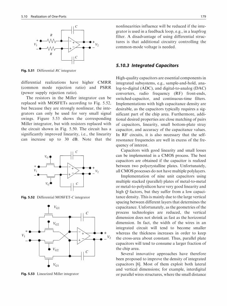
differential realizations have higher CMRR
(common mode rejection ratio) and PSRR
(power supply rejection ratio).
The resistors in the Miller integrator can be
replaced with MOSFETs according to Fig. 5.52,
but because they are strongly nonlinear, the inte-
grators can only be used for very small signal
swings. Figure 5.53 shows the corresponding
Miller integrator, but with resistors replaced with
the circuit shown in Fig. 5.50. The circuit has a
significantly improved linearity, i.e., the linearity
can increase up to 30 dB. Note that the
nonlinearities influence will be reduced if the inte-
grator is used in a feedback loop, e.g., in a leapfrog
filter. A disadvantage of using differential struc-
tures is that additional circuitry controlling the
common-mode voltage is needed.
5.10.3 Integrated Capacitors
High-quality capacitors are essential components in
integrated subsystems, e.g., sample-and-hold, ana-
log-to-digital (ADC), and digital-to-analog (DAC)
converters, radio frequency (RF) front-ends,
switched-capacitor, and continuous-time filters.
Implementations with high capacitance density are
desirable, as the capacitors typically requires a sig-
nificant part of the chip area. Furthermore, addi-
tional desired properties are close matching of pairs
of capacitors, linearity, small bottom-plate stray
capacitor, and accuracy of the capacitance values.
In RF circuits, it is also necessary that the self-
resonance frequencies are well in excess of the fre-
quency of interest.
Capacitors with good linearity and small losses
can be implemented in a CMOS process. The best
capacitors are obtained if the capacitor is realized
between two polycrystalline plates. Unfortunately,
all CMOS processes do not have multiple polylayers.
Implementation of nine unit capacitors using
multiple stacked (parallel) plates of metal-to-metal
or metal-to-polysilicon have very good linearity and
high Q factors, but they suffer from a low capaci-
tance density. This is mainly due to the large vertical
spacing between different layers that determines the
capacitance. Unfortunately, as the geometries of the
process technologies are reduced, the vertical
dimension does not shrink as fast as the horizontal
dimension. In fact, the width of the wires in an
integrated circuit will tend to become smaller
whereas the thickness increases in order to keep
the cross-area about constant. Thus, parallel plate
capacitors will tend to consume a larger fraction of
the chip area.
Several innovative approaches have therefore
been proposed to improve the density of integrated
capacitors [6]. Most of them exploit both lateral
and vertical dimensions; for example, interdigital
or parallel wires structures, where the small distance
C
V1
R
+_ V2
RC
Fig. 5.51 Differential RC integrator
C
+_
C
VG
VG
V1 V2
Fig. 5.52 Differential MOSFET-C integrator
C
V1+_ V2
C
VG1
VG2
VG2
VG1
Fig. 5.53 Linearized Miller integrator
5.10 Realization of One-Ports 179

between two wires in the same layer is used as a
capacitor. Many complex structures that exploit
both interlayer and intralayer capacitors are possi-
ble [6]. In addition, higher capacitance density can
be achieved by using insulators with higher dielec-
tric constant.
Some circuits, e.g., SC filter, exploit the fact that
the ratio of two capacitors can be very accurate,
but their absolute values are of less importance.
Figure 5.54 shows a typical layout of two matched
capacitors, which consist of nine unit capacitors.
The ratio of the two capacitances can be very
accurate (0.1%), while the accuracy of the absolute
values may be of the order 10%. The capacitors in
the four corners and in the center constitute one of
the capacitors and the others the second one. Unity
capacitors are used to reduce the edge effects.
5.10.4 Inductors
5.10.4.1 Integrated Inductors with Passive
Components
Inductors can be integrated on various substrates,
e.g., thin film and silicon [25]. Magnetic material is
rarely used, and the inductances that can be imple-
mented using high-density technologies are rela-
tively small. Furthermore, the Q factors are often
in the range 5–20 on silicon substrates, which often
is too low for many applications. The effective Q
factors can, of course, be increased by combining a
passive coil and an active circuit that realizes a
negative resistor. For high-performance integrated
filters, however, inductorless, or more correctly
coil-less solutions are used in practice because inte-
grated coils have too low Q factors.
5.10.4.2 Integrated Inductors with Active
Components
An inductor can be realized by using Antoniou’s
GIC. There exist several alternative selections of
the circuit elements in the GIC. The input impe-
dance, with nonideal operational amplifiers, is
Zin ¼Z1Z3Z5 þ Z1ðZ4 þ Z5Þ Z2
A1þ Z3
A2þ Z2þZ3þZ2Z3Ys
A1A2
Z2ðZ4 YsZ5Z3Þ þ ðZ4 þ Z5Þ Z2
A1þ Z3
A2þ Z2þZ3þZ2Z3Ys
A1A2
: (5:74)
5.10.4.3 Antoniou’s GIC of Type A
There are several ways of choosing the impedances
Z1 through Z5 so the circuit shown in Fig. 5.41 rea-
lizes, for example, an inductor. By choosingZ1=R1,
Z2=1/sC2,Z3=R3,Z4=R4, andZ5,=R5, a GIC
of type A is obtained. The input impedance is
Zin ¼ Ls
where L = R1R3R5C2/R4.
It can be shown using Equation (5.74) that the
effect of the finite bandwidths of the amplifiers is
minimized if we select
ot1R5 ¼ ot2R4: (5:75)
Antoniou’s GIC is sensitive for stray capaci-
tances parallel with R5. The detrimental effect of a
Fig. 5.54 Layout of two matched capacitors consisting of
nine unti capacitrs
180 5 Basic Circuit Elements

stray capacitanceCp can for type A be compensated
with a capacitance Cs = CpR4/R3 between the
operational amplifier’s inverted input and ground.
5.10.4.4 Antoniou’s GIC of Type B
By choosing Z1 = R1, Z2 = R2, Z3 = R3, Z4 = 1/
sC4, and Z5 = R5, a GIC of type B is obtained with
the input impedance
Zin ¼ Ls
where L = R1R3R5C4/R2.
Usually the B type is used, also called type II,
because it has better high frequency properties, i.e., is
less sensitive for the amplifier’s finite gain-bandwidth
products, GB [112]. It is advisable to choose [106]
Z2 ¼ Z3 ¼ R (5:76)
to obtain good high-frequency properties and to use
matched amplifiers.
The detrimental effect of a stray capacitance Cp
at port 2 can for type B be compensated with a
resistance Rs = C4R3/Cp between the operational
amplifier’s inverted input and ground.
5.10.4.5 Transconductor-Based Inductors
A grounded gm-C inductor with the inductance
L ¼ C=gm1gm2 can be realized with a gyrator
according to Fig. 5.55.
Figure 5.56 shows the corresponding small-
signal model where the input and output impedances
have been included in the model [18].
We get by summing the currents in the output
and input nodes
gm1Vin þ ðYout1 þ Yin2 þ sCÞV2 ¼ 0
Iin ¼ Yin1Vin þ I2
I2 ¼ Yout2Vin þ gm2V2
8
>
<
>
:
where
Yin1 ¼ Gi1 þ sCi1
Yout1 ¼ G01 þ sC01
Yin2 ¼ Gi2 þ sCi2
Yout2 ¼ G02 þ sC02:
We get the input admittance
Yin ¼ Yin1 þ Yout2 þgm1gm2
Yin2 þ Yout1 þ sC
and after simplification
Yin ¼ G1 þ sC1 þgm1gm2
G2 þ sC2
(5:77)
where
G1 ¼ Gi1 þ G01 G2 ¼ Gi2 þ G02
C1 ¼ Ci1 þ C02 C2 ¼ Ci2 þ C01 þ C:
The inductor has the inductance
L ¼ C
gm1gm2
and the parasitic elements in the model of a
grounded inductor that is shown in Fig. 5.57
V1
C
gm1
gm2
Fig. 5.55 Realization of a
grounded inductor
I1
C01gm1(0 – Vin)
G01
Ci1
Gi1
Gi2
Ci2
G02
C02
I2
CVin
Iin
V2
gm2(Vout – 0)
Fig. 5.56 Small-signal model for the grouded inductor
5.10 Realization of One-Ports 181

Ls ¼Ci1 þ C02
gm1gm2
Rs ¼G01 þ Gi2
gm1gm2
Cp ¼ Ci1 þ C02 Rp ¼1
Gi1 þ G02
:
For two identical gyrators with Gi1 = Gi2, Ci1 =
Ci2, G01 = G02, C01 = C02, and gm1 = gm2, which is
the requirement for the gyrators being lossless, we
get the Q factor for the inductor
QL ¼ oL
Rs
¼ oCi2 þ C02 þ C
ðGi2 þ G02Þ:
For example, a gm-C inductor with the induc-
tance 100 mH at o= 2p 10 MHz obtains a Q factor
of more than 3000 ifG02=0.1 mS and gm=220 mS.
This is a high Q factor.
A floating inductor can be realized according to
Fig. 5.10 using the gyrator shown in Fig. 5.42. The
circuit corresponds to a shunt capacitor between
two gyrators. It is advantageous to use grounded
capacitors because the voltage over the bottom
plate stray capacitance is not changed. This circuit
can, however, be simplified according to Fig. 5.58,
where gm1 = gm3 and the series inductor is L = C/
(gm2gm3).
A grounded inductor requires two transconduc-
tors whereas a floating inductor requires three.
A floating parallel resonance circuit, which is
difficult to realize because it contains a floating
capacitor, can thus be realized with two gyrators
and a grounded series resonance circuit as shown in
Fig. 5.59. The element values in the realized series
resonance circuit are
L0 ¼ C
gm2gm3
C 0 ¼ 1
Lgm2gm3
where gm1 = gm3 and. The series resonance circuit
can then be realized in two different ways.
Figure 5.60 shows the case with grounded inductor
RpL
Cp
LsRs
Zin
Fig. 5.57 Small-signal model for the grounded inductor
C
gm1gm2
V1 V2
gm3
Fig. 5.58 Simplified realization of a floating inductor
L
C
gm1gm2
V1 V2
L’
C’
gm3
Fig. 5.59 Realization of a floating parallel resonance
circuit
gm
gm
C ’
C ’
L ’
Floating node
C ”
Fig. 5.60 Realization of a series resonance circuit with afloating node
182 5 Basic Circuit Elements

and floating capacitor, which is a poorer realiza-
tion, as it has a floating node where the stray capa-
citance of C 0 will have a large effect.
Figure 5.61 shows the case with a grounded capa-
citor and floating inductor, which requires three
transconductors, but has no floating nodes, which
makes it more suitable for implementation.
5.10.4.6 Current Conveyor-Based Inductors
Integrated inductors can of course also be imple-
mented by using current conveyors [144].
5.10.5 FDNRs
An FDNR can be realized by Antoniou’s GIC.
Here we are only interested in supercapacitors
because superinductors have very poor frequency
performance. We have several alternative selections
of the elements in the GIC, which mainly differs
with respect to the sensitivity to the bandwidth of
the operational amplifiers. The best realization of a
supercapacitor is obtained by selecting Z1 = 1/sC1,
Z2 = R2, Z3 = R3, Z4 = R4, and Z5 = 1/sC5. In
order to minimize the influence of finite bandwidths
of the amplifiers, we should select
R2 ¼ R3: (5:78)
A supercapacitor can also be realized by cascad-
ing two lossless integrators that can be realized
by, e.g., tranconductors and current conveyors.
Figure 5.62 shows a current conveyor circuit that
realizes a supercapacitor with the value
D ¼ C1C2R
a1a2(5:79)
where a1 and a2 are the current gains for CCII+
and CCII–, respectively. An operational amplifier
(transconductance) of type OPA2662 typically has
the current gains a1 = 3.1 and a2 = 2.9.
5.11 Problems
5.1 a) Show that
|Z|2 = Z Z*.
b) 2 ReZ = Z + Z*.
c) If V= Vr + j Vi and I= Ir + j Ii, then P=
ReVI* = VrIr + Vi Ii.
5.2 Determine which of the following circuit ele-
ments are passive and lossless:
a) resistor
b) inductor
c) capacitor
d) negative inductor (L)
e) negative capacitor (C)
f) negative resistor (R)
5.3 Determine the K matrix for a two-port consist-
ing of
a) a series impedance
b) a shunt admittance
L ’
C ’
C ’
gm2
gm1
gm3
C ”
Fig. 5.61 Realization of a series resonance circuit without
floating node
Vin
IinCCII+
y
x
z CCII–
y
x
z
R
Ix2
+
–
C1 C2
Fig. 5.62 Supercapacitor
5.11 Problems 183

5.4 Derive the K matrix for
a) VCVS
b) VCCS
c) CCVS
d) CCCS
5.5 Derive the inverse of the K matrix in terms ofA,
B, C, and D.
5.6 Use the K matrix to determine the transfer func-
tion for a third-order T ladder with Rs = RL =
600 O, L1 = L3 = 600 mH, and C2 = 3.3 mF.
5.7 Determine the K matrix for the LC network
shown in Fig. 3.5.
5.8 a) Determine the K matrix for the two-port
shown in Fig. 5.63 when the operational
amplifier is assumed to be ideal.
b) Determine the input impedance to the two-
port.
5.9 a) Determine the input impedance to the cir-
cuit shown in Fig. 5.64 by using chain
matrices. Identify the type of two-port
when Z5 is considered to be the load
impedance.
b) Determine the input impedance when
Z1Z3 ¼ Z2Z4.
5.10 Determine the transconductance, gm = I2/
V1, for the circuit shown in Fig. 5.65 and pro-
pose how it can be used in a possible
application.
5.11 Determine the poles and zeros of the transfer
functions for the inverting and noninverting
amplifiers shown in Fig. 5.27 and 5.28 when
Z1 and Z2 are resistors.
a) R1 = R2 = 10 kO
b) R1 = 10 kO and R2 = 100 kO
c) R1 = 1 and R2 = r = 10 kO
The amplifiers are nonideal and are mod-
eled with the simple single-pole model with
A0 = 2105 and a real pole sp = 100 rad/s.
Determine the 3 dB bandwidth of the circuits.
5.12 Determine suitable values for the resistor r in
the circuits shown in Figs. 5.28 and 5.29. What
is the function of the resistor? How should the
resistor, r, be selected if R2 in the inverting
amplifier is changed to a capacitor?
5.13 Estimate A0, o3dB, and ot for the operational
amplifier MAX426x that has a 3 dB band-
width of 450 MHz when the open-loop gain
equals 1 and gain = 10 at 50 MHz.
5.14 Propose a model that includes the frequency
response for the inverting amplifier, shown in
Fig. 5.27. The model should only contain pas-
sive components and an ideal operational
amplifier. Hint: Place an extra impedance in
parallel with Z2.
5.15 Derive the transfer function for the Miller
integrator shown in Fig. 5.32. Determine the
poles and zeros when R = 10 kO, C = 10 pF,
A0 = 105, and o3dB = 100 rad/s.
R1 R3
R2 V2V1
_
+
I1 I2
Fig. 5.63 Two-port in problem 5.8
Z1
Zin
Z2 Z3 Z4
Z5
Fig. 5.64 One-port in problem 5.9
V1
R1
R2 R3
R4
I2
Z
Fig. 5.65 Circuit in problem 5.10
184 5 Basic Circuit Elements

5.16 Derive the transfer function for the Deboo inte-
grator shown in Fig. 5.66. Determine the poles
and zeros when all resistors are equal, e.g., R =
10 kO andC = 10 pF, A0 = 105 and o3dB =
100 rad/s. The integrator is sensitive for resistor
ratio mismatch and is not recommended.
5.17 Determine the transfer functions for the cir-
cuits shown in Figs. 5.67, 5.68, and 5.69.
5.18 Derive Equation (5.79).
5.19 Propose a circuit with only one operational
amplifier that realizes the function: Vout =
2V1 – 5V2 where V1 and V2 are inputs.
5.20 Determine the output signal V3 as a function
of V1 and V2 for the circuit shown in Fig. 5.70.
5.21 Determine the output signal V3 as a function
of V1 and V2 for the circuit shown in Fig. 5.71.
Vin C
Vout
_
+
R4
R1
R2
R3
Fig. 5.66 Circuit in problem 5.17
C
Vin Vout
R
+
_
A1
A2
Fig. 5.68 Circuit in problem 5.17
VinVout
R2 C2
C1
R1
_
+
Fig. 5.67 Circuit in problem 5.17
Vin
Vout
R2R2
R5
R4
R3
R1
C1
_
+
Fig. 5.69 Circuit in problem 5.17
V1
V2V3
gm1
gm2
gm3
Fig. 5.70 Transconductor circuit in problem 5.20
5.11 Problems 185

5.22 Determine the chain matrix and identify the
two-port that is realized by the circuit shown
in Fig. 5.72.
5.23 Determine a suitable value for the resistor, rx,
shown in Fig. 5.73, to compensate for the finite
bandwidth of the amplifier. Select the element
values R= 22 kO and C= 10 nF. The opera-
tional amplifier has very low power consump-
tion and has therefore low bandwidth, e.g.,
ot = 100 krad/s.
5.24 Determine theQ factor for the circuit shown in
Fig. 5.74 and the resonance frequency when
R=10 kO, C1 =10 nF, C2 =27 nF, and r=
500 O.
5.25 a) Derive the input impedance to the circuit
shown in Fig. 5.41 assuming that the opera-
tional amplifiers are ideal.
b) Determine the K matrix for the circuit
where Z5 is the load impedance.
5.26 Use Antoniou’s GIC to realize an
a) inductor with inductance L = 300 mH
b) supercapacitor with D = 108 Fs
5.27 Determine the admittance between the opera-
tional amplifiers’ inverting inputs and ground
in Antoniou’s GIC so that a stray capacitor at
the output of the circuit is compensated when
Z1= R1, Z2 = R2, Z3 = R3, and Z4 = 1/sC4.
Assume that Z5 consists of R5 in parallel with
1/sCstray and that the operational amplifiers
are ideal.
5.28 Determine suitable element values to realize
an inductor with inductance 100 mH when
there is a stray capacitor of 10 pF in par-
allel with Z5.
5.29 Determine the admittance Ys in Problem 5.27
so that a stray capacitor at the output of the
circuit is compensated when the circuit shall
realize a supercapacitor with D = 109 Fs.
5.30 Derive Equation (5.55).
+
_Vin
Vout
I1
I2
CCII
y
x
z
+
Fig. 5.72 Current conveyor circuit in problem 5.21
C
V1
R – rx
rx
V2
A(s) +
_
Fig. 5.73 Compensated integrator used in problem 5.23
r
V1
C2C1
R
Fig. 5.74 Gyrator circuit in problem 5.24
C
V1
V2V3
gm1
gm2
Fig. 5.71 Transconductor
circuit in problem 5.21
186 5 Basic Circuit Elements

Chapter 6
First- and Second-Order Sections
6.1 Introduction
Many active filter structures are based on first- and
second-order sections. In this chapter, we will first
discuss different types of sections with respect to
their transfer functions. Next, we will classify, ana-
lyze, and compare different realizations that are
based on resistors, capacitors, and with one or sev-
eral operational amplifiers, transconductors, or cur-
rent conveyors [58, 130]. These circuits can, of
course, be implemented with discrete components,
but this is of less interest because a large number of
active elements are often needed and the cost and
the power consumption becomes high. Integrated
active elements are considerably cheaper and con-
sume less power.
A problem with integrating analog circuits is that
the capacitors require large chip area and that the
tolerances in the capacitance values vary signifi-
cantly due to variations in the manufacturing pro-
cess. The resistance values are restricted to a rela-
tively small interval and the tolerances in the
resistance values vary significantly as well.
In SC filters, circuit techniques are used that are
based on the fact that the frequency response
depends on the ratio between two capacitances
and not on the absolute capacitance values. The
error in the ratio between two capacitances can be
made less than 0.1% even though the capacitance
values can vary –10% or more. The capacitors
dominate the chip area required for an integrated
analog filter. Typically, the total capacitance, which
can currently be economically integrated on a chip,
is less than 30 pF.
Circuit techniques that rely on ratios of compo-
nent values are not directly applicable for integrated
active filters. Instead, special circuits for tuning of
the frequency response are used because the active
elements and capacitance values vary strongly and
the filter properties depend on the absolute values.
The tuning must also be made while the filter is
operating because the element values vary with the
temperature and the power supply voltage.A large
number of transconductor-C filters are manufac-
tured and used in, e.g., the read and write channels
in hard drives. These filters are programmable
because the bandwidth must be adjusted depending
on which track is being accessed.
Transconductor-C filters and other methods
for integrating analog filters are active research
topics due to the trend to integrate whole signal
processing systems on a single chip. Integrating a
whole system tends to reduce the physical size
and power consumption, and cost is therefore
suitable for manufacturing cheap consumer pro-
ducts in large volumes.
6.2 First-Order Sections
A first-order section can either be of lowpass (LP),
highpass (HP), or allpass (AP) type.
6.2.1 First-Order LP Section
The transfer function for a first-order LP
section is
L. Wanhammar, Analog Filters Using MATLAB, DOI 10.1007/978-0-387-92767-1_6,
Springer ScienceþBusiness Media, LLC 2009
187

HðsÞ ¼ G
s sp
(6:1)
with a real pole on the negative real axis and one
zero at s=1. Figure 6.1 shows the magnitude and
phase functions for a first-order LP section with a
real pole for the two cases sp1 = 1 rad/s and
sp2 = 5 rad/s. By choosing G = sp, the magni-
tude function is normalized to 1 foro=0.Note that
the magnitude function decays faster the closer the
pole is to the jo-axis. The phase goes from 0 top/2.
According to Equation (5.27), an operational
amplifier can thus be modeled with a first-order
transfer function withG=A0o3dB and sp=o3dB.
6.2.2 First-Order HP Section
The transfer function for a first-order HP
section is
HðsÞ ¼ Gs
s sp
: (6:2)
Figure 6.2 shows the magnitude and phase
functions for a first-order highpass section with a
real pole for the two cases sp1 = 1 rad/s and
sp2 = 5 rad/s and a zero at the origin. The gain
at high frequencies has been normalized to 1 by
choosing G = 1.
6.2.3 First-Order AP Section
The transfer function for a first-order AP
section is
HðsÞ ¼ Gs sz
s sp
(6:3)
where sz = sp. The poles and the zeros for an
allpass section lie symmetrically around the jo-axis.
0 5 10 15 200
0.2
0.4
0.6
0.8
1
ω [rad/s]
–90
–72
–54
–36
–18
0
σp2 = –5 rad/s
σp1 = –1 rad/s
Φ2
Φ1
|H1|
|H2||H
(jω
)|
Φ(ω
) [
deg
rees
]
jω
σ×σp
1 zero at ∞
Fig. 6.1 Pole-zeroconfiguration and
magnitude and phase
functions for a first-order LPsection for the two cases
sp1 ¼ 1 rad=s andsp2 ¼ 5 rad=s
0 5 10 15 200
0.2
0.4
0.6
0.8
1
ω [rad/s]
0
18
36
54
72
90
|H(j
ω)|
Φ(ω
) [d
egre
es]
σp1 = –1 rad/s
σp2 = –5 rad/s
Φ1
Φ2
|H1|
|H2|jω
σ×σpFig. 6.2 Pole-zero
configuration and
magnitude and phasefunctions for a first-order
HP section for the two cases
sp1 ¼ 1 rad=s andsp2 ¼ 5 rad=s
188 6 First- and Second-Order Sections

Figure 6.3 shows the magnitude and phase func-
tions for an allpass filter for the two cases sp1 =
1 rad/s and sp2 = 5 rad/s where G = 1, i.e.,
|H(jo)| = 1.
6.3 Realization of First-Order Sections
The first-order sections of LP and HP type can be
realized with simple RC sections according to
Fig. 6.4. The sections must, however, be driven by
a low impedance signal source, e.g., an operational
amplifier. Furthermore, if a section has high out-
put impedance, it cannot be loaded by a subse-
quent circuit. In this case, we must use a buffer
amplifier with high impedance input and low impe-
dance output. In some cases, a first-order section is
combined with a second-order section into a third-
order section to reduce the number of operational
amplifiers.
The LP and HP sections have the transfer
functions
HðsÞ ¼ 1
RC 1
sþ 1
RC
(6:4)
and
HðsÞ ¼ s
sþ 1
RC
(6:5)
respectively. To reduce the influence of the bias cur-
rents, a resistorR should be inserted into the feedback
loop. Henceforth, we will always explicitly show these
resistors in order to simplify the schematics.
Theorem 6.1 A lowpass filter that is realized by a
linear active RC network is converted to a highpass
filter if all resistors and capacitors are replaced by
capacitors and resistors, respectively.
An amplifier is required in order to realize a first-
order AP section. Figure 6.5 shows an example of a
first-order AP section with the transfer function
HðsÞ ¼ s 1RC
sþ 1RC
(6:6)
where we select R1 R/2 in order to minimize the
offset voltage due to the bias currents.
Figure 6.6 shows a first-order gm-C section with
two transconductors. We have for the circuit
0 5 10 15 200
0.2
0.4
0.6
0.8
1
ω [rad/s]
0
36
72
108
144
180
σp1 = –1 rad/s
σp2 = –5 rad/s
Φ1
Φ2|H(j
ω)|
Φ(ω
) [d
egre
es]
|H|jω
σ×σp σz
Fig. 6.3 Pole-zero
configuration andmagnitude and phase
functions for a first-order AP
section for the two cases
sp1 ¼ 1 rad=s andsp2 ¼ 5 rad=s
Vin
R
CVout
+
_
+
_
VoutR
C
Vin
Fig. 6.4 Realization of
first-order LP and HP
sections
6.3 Realization of First-Order Sections 189

I1 ¼ gm1Vin
I2 ¼ gm2Vout
I1 þ I2 ¼ sCVout :
8
<
:
After simplification we obtain
HðsÞ ¼ Vout
Vin
¼ gm1
C
1
sþ gm2
C
:
6.4 Second-Order Sections
A general transfer function of the second order with
a complex-conjugated pole pair sp = sp – jop and
arbitrary zeros can be written
HðsÞ ¼ as2 þ bsþ c
s2 2spsþ r2p(6:7)
where the pole radius, rp, is
rp ¼ffiffiffiffiffiffiffiffiffiffiffiffiffiffiffiffi
s2p þ o2p
q
: (6:8)
Two poles on the real axis are obtained if rp sp/2. By choosing different values of a, b, and c, a
number of interesting special cases of the second-
order sections are obtained.
Theorem 6.2 A necessary condition for a polynomial
to be Hurwitz is that all coefficients of s are present,
i.e., 6¼ 0, and have the same sign.
Thus, if any of the terms is missing or has a
different sign, at least one root (pole) will lie in the
right half plane.
6.4.1 Second-Order LP Section
The transfer function for a second-order LP
section is
HðsÞ ¼ G
s2 2spsþ r2p: (6:9)
The corresponding pole-zero configuration, mag-
nitude and phase response is shown in Fig. 6.7. The
transfer function has two zeros at s = 1. The pole
radius can be determined with high accuracy by
measuring the frequency for which the phase func-
tion is 908 as HðjrpÞ ¼ G=ðspjrpÞ and 2sp =
o45 o135, whereo45 and o135 are the angular
frequencies for which the phase is 458 and 1358,
respectively.
gm1
Vin
C
I1I2 Vout
gm2––
Fig. 6.6 First-order LP section
jω
σ
×
×
σp
jωp
–jωp
rp Φ
0 5 10 15 200
0.2
0.4
0.6
0.8
1
1.2
1.4
1.6
1.8
2
ω [rad/s]
–180
–144
–108
–72
–36
0
σp2 = –3 rad/s
Φ2
Φ1
|H1|
|H(j
ω)|
Φ(ω
) [
deg
rees
]σp1 = –1 rad/s
|H2|Fig. 6.7 Pole-zero
configuration andmagnitude and phase
functions for a second-order
LP section with rp ¼ 3 rad=sand G ¼ rp
2
R
+
_
C
Vin
Vout
R1 R1
Fig. 6.5 First-order AP section
190 6 First- and Second-Order Sections

6.4.1.1 Q Factor for a Pole Pair
The transfer function for an LP section can also be
written
HðsÞ ¼ G
s2 þ rp
Q
sþ r2p
(6:10)
where the Q factor (quality factor) of the poles is
defined as
Q D¼ rp
2sp
: (6:11)
According to Equation (6.11), the Q factor
depends on the angle between the jo-axis and the
vector from origin to the pole. TheQ factor for a real
pole is 0.5. The Q factor for a resonance circuit is
defined according to Definition 3.1 as the ratio
between maximum stored energy and dissipated
energy during a period. Figure 6.8 shows the
magnitude function for different Q factor when
rp = 3 rad/s. The magnitude function at o = 0 has
been normalized to 1 by choosing G ¼ r2p.
There is a peak in the magnitude function if
Q41=ffiffiffi
2p
and it occurs at
opeak ¼ rp
ffiffiffiffiffiffiffiffiffiffiffiffiffiffiffiffiffi
1 1
2Q2
s
: (6:12)
The Q factor is a simple measure of how difficult
it is to implement a second-order transfer function.
It is therefore customary to classify pole pair in
second-order sections with respect to the Q factor
for the poles according to
low Q factors : Q 2
medium high Q factors : 25Q 20
high Q factors : Q420
Example 6.1 Determine the pole radius and the Q factorfor the pole pair, sp = 0.25 – j0.95 krad/s. The pole radius
is rp ¼ffiffiffiffiffiffiffiffiffiffiffiffiffiffiffiffiffi
s2p þ o2
p
q
¼ffiffiffiffiffiffiffiffiffiffiffiffiffiffiffiffiffiffiffiffiffiffiffiffiffiffiffi
0:252 þ 0:952p
¼ 0:9823441 krad=s and
the Q factor is Q ¼ rp
2sp
¼ 0:9823441
2 ð0:25Þ ¼ 1:9646883.
The largest change of the magnitude function
due to errors in the Q factor and the pole radius
is obtained in the proximity of the resonance
frequency.
Figure 6.9 shows the variation in the magnitude
function when the Q factor and the pole radius is
varied with –5% where the nominal pole radius is
rp = 3 rad/s. From the figure, it is evident that the
magnitude function is very sensitive for variations
in the pole radius whereas an error in the Q factor
has less influence. It can be shown that the variation
of the magnitude function is proportional to
0 2 4 6 80
1
2
3
4
5
6
7
ω [rad/s]
|H(j
ω)|
1
2
3
4
5
6
Fig. 6.8 Magnitude function for pole pairs with different Q
factors
0 2 4 60
5
10
15
20
25
ω [rad/s]
0 2 4 60
5
10
15
20
25
ω [rad/s]
|H(j
ω)|
|H(j
ω)|
–5%
+5%
Fig. 6.9 Variation in themagnitude function due to a
5% variations in the Q
factor (left) and pole radius
(right). Q = 20
6.4 Second-Order Sections 191

DjHjjHj / DQ
Q(6:13)
and
DjHjjHj / 2Q
Drp
rp: (6:14)
The influence on the magnitude function, due to
an error in the Q factor, is proportional to the error
in Q factor, whereas the influence of an error in the
pole radius is much larger for large Q factors.
It can be shown that similar relations as Equa-
tions (6.13) and (6.14) are valid for the phase func-
tion as well. It is therefore essential to use realiza-
tions of the sections in which any deviation from the
nominal component values have small influence on
the pole radius. In this chapter, we will therefore
focus on this issue when we compare different reali-
zations of second-order sections.
6.4.2 Second-Order HP Section
The transfer function for a second-order HP section
(highpass section) is
Hs ¼ Gs2
s2 2spsþ r2p¼ Gs
2
s2 þ rpQ
sþ r2p
: (6:15)
The transfer function has two zeros at the origin.
The pole radius in Fig. 6.10 is rp = 3 rad/s and the
gain at high frequencies has been normalized to 1 by
choosingG=1.An implementation of aHP section
will of course have finite bandwidth due to parasitic
capacitances and the active element’s finite band-
width, but this will occur at such high frequencies
that are of no interest.
The phase function at s = jrp is +908. The peak
of the magnitude function occurs at
o ¼ rpffiffiffiffiffiffiffiffiffiffiffiffiffiffiffiffiffi
1 1
2Q2
s : (6:16)
6.4.3 Second-Order LP-Notch Section
The transfer function for a second-order LP-notch
section (lowpass-notch section) is
HðsÞ ¼ Gðs2 þ r2zÞs2 2spsþ r2p
¼ Gðs2 þ r2zÞs2 þ rp
Q
sþ r2p
; rz4rp: (6:17)
The transfer function has a complex conjugating
zero pair on the jo-axis at o = rz. The frequency
response becomes equal to zero for this frequency.
The pole radius, shown in Fig. 6.11, is rp = 3 rad/s,
and the zero pair has the radius rz = 6 rad/s.
For high frequencies, the magnitude function
approaches G, which has here been set to G =
(rp/rz)2. Note that for an LP-notch section, the
radii of the poles are smaller than that of the
zeros and that the phase function jumps p at a
zero at the jo-axis.
If the pole radius the zero radius, we have a
second-order LP notch filter, i.e., a filter with
jω
jωp
–jωp
σ
×
×
σp
rp
0 5 10 15 200
0.2
0.4
0.6
0.8
1
1.2
1.4
1.6
1.8
2
ω [rad/s]
0
18
36
54
72
90
108
126
144
162
180
σp2 = –3 rad/s
Φ2
Φ1
|H1|
|H(j
ω)|
σp1 = –1 rad/s
|H2|
Φ(ω
) [
deg
rees
]
Fig. 6.10 Pole-zero
configuration and
magnitude and phasefunction for a second-order
HP section
192 6 First- and Second-Order Sections

approximately constant magnitude function, except
for a notch at the zero. Such filters can be used as
simple bandstop filters, i.e., to attenuate disturbances
originating from the mains (50 or 60 Hz).
6.4.4 Second-Order HP-Notch Section
An HP-notch section is obtained if instead the pole
radius is larger than the zero radius, as shown in
Fig. 6.12. The transfer function for a second-order
HP-notch section (highpass-notch section) is
HðsÞ ¼ Gðs2 þ r2zÞs2 2spsþ r2p
¼ Gðs2 þ r2zÞ
s2 þ rp
Q
sþ r2p
; rz5rp: (6:18)
The transfer function has a finite zero pair. The
pole radius, shown in Fig. 6.12, is rp = 3 rad/s, and
the complex conjugating zero pair has the radius
rz = 2 rad/s and G = 1. The phase jumps p at
the zero on the jo-axis.
6.4.5 Second-Order BP Section
The transfer function for a second-order BP
section (bandpass section) is
HðsÞ ¼ Gs
s2 2spsþ r2p¼ Gs
s2 þ rp
Q
sþ r2p
: (6:19)
jωz = jrz
jωp
–jωp
–jωz
jω
σ
×
×
σp
rp
0 5 10 15 200
0.2
0.4
0.6
0.8
1
1.2
1.4
ω [rad/s]
–180
–144
–108
–72
–36
0
36
72
σp2 = –3 rad/sΦ2
Φ1
|H1|
σp1 = –1 rad/s
|H2|
Φ(ω
) [d
egre
es]
|H(j
ω)|
Fig. 6.11 Magnitude andphase functions and
corresponding pole-zero
configuration for a second-
order LP-notch section withG ¼ ðrp=rzÞ2
jω
σ
×
×
σp
jωp
–jωp
rpjωz
–jωz
0 5 10 15 200
0.2
0.4
0.6
0.8
1
1.2
1.4
ω [rad/s]
–90
–54
–18
18
54
90
126
162
σp2 = –3 rad/s
Φ1
|H1|
σp1 = –1 rad/s
|H2|
Φ(ω
) [d
egre
es]
|H(j
ω)|
Φ2Fig. 6.12 Pole-zeroconfiguration and
magnitude and phase
functions for a second-orderHP-notch section
6.4 Second-Order Sections 193

The pole radius, shown in Fig. 6.13, is rp=3 rad/
s and G=rp. The transfer function has a finite zero
at s = 0 and one at s = 1. The peak of the
magnitude function occurs at o = rp. The phase
function at s = jrp is 08.
6.4.5.1 Second-Order AP Section
The transfer function for a second-order AP section
(allpass section) is
HðsÞ ¼ Gs2 2szsþ r2zs2 2spsþ r2p
(6:20)
where the poles are
sp ¼ sp jop
and the zeros, which equal the poles mirrored in the
jo-axis, are
sz ¼ sz joz ¼ sp jop:
The magnitude function is constant, but the sec-
tion has a frequency-dependent phase function.
Allpass sections are often used for correction of
the phase function of a filter by placing AP sections
in series with the filter so the total phase function
becomes approximately linear. The AP section,
which has its zeros in the right half plane, is a
maximum-phase filter.
6.4.6 Element Sensitivity
As a measure of sensitivity of a function, Y, with
respect to a parameter, x, we use the ratio of the
normalized derivatives.
Definition 6.1 The element sensitivity is defined as
SYxD¼x
Y
@Y
@x: (6:21)
jω
σ
×
×
σp
jωp
–jωp
rp
0 5 10 15 200
0.2
0.4
0.6
0.8
1
1.2
1.4
1.6
ω [rad/s]
–90
–45
0
45
90
σp2 = –3 rad/s
Φ2
Φ1
|H1| σp1 = –1 rad/s
|H2|
Φ(ω
) [d
egre
es]
|H(j
ω)|
Fig. 6.13 Pole-zeroconfiguration and
magnitude and phase
functions for a second-order
BP section
jω
σ
×
×
σz
jωp
–jωp
σp
rp rp
0 5 10 15 200
0.2
0.4
0.6
0.8
1
1.2
ω [rad/s]
–180
–120
–60
0
60
120
180
σp2 = –3 rad/sΦ2
Φ1
|H |
σp1 = –1 rad/s
Φ(ω
) [d
egre
es]
|H(j
ω)|
Fig. 6.14 Pole-zeroconfiguration and
magnitude and phase
functions for a second-orderallpass section
194 6 First- and Second-Order Sections

For an LP second-order section, we have
SHðsÞQ ¼ rp
Q s
DðsÞ (6:22)
and
SHðsÞrp
¼ rp
Q sþ 2rpQ
DðsÞ (6:23)
where D(s) is the denominator of a second-order
transfer function. The numerator in Equation
(6.22) has a zero at s = 0 whereas Equation (6.23)
has a zero on the negative real axis, far from the
origin. Hence, the sensitivity of the transfer function
with respect to Q is much less than the sensitivity
with respect to rp. Thus, we have, if o << 2rpQ and
Q >> 1,
SHð joÞQ
55 SHð joÞrp
: (6:24)
The difference in sensitivity was earlier illu-
strated in Fig. 6.9. According to Equations (6.13)
and (6.14), the influence of errors in the pole radius
is about 2Q times larger than for corresponding
error in the Q factor. Hence, we should therefore
only use second-order sections where the errors in
the element values have minimal influence on the
pole radius and we will henceforth only discuss sec-
tions that have minimal pole radius sensitivity.
The sensitivity of the pole radius for errors in a
resistor and capacitance are
SrpRD¼R
rp
@rp@R
(6:25)
and
SrpCD¼C
rp
@rp@C
: (6:26)
For a useful second-order section, the sensitivi-
ties SrpR and S
rpC for all R and C elements should be
small. For all second-order sections, we have
X
i
SrpRi
¼X
i
SrpCi
¼ 1 (6:27)
X
i
SQRi
¼X
i
SQCi
¼ 0: (6:28)
6.4.7 Gain-Sensitivity Product
As ameasure of sensitivity of the poles radius andQ
factor due to the finite amplifier gain,A0, we use the
gain-sensitivity product that is defined for the pole
radius [105, 106, 112].
Definition 6.2 The gain-sensitivity product for the
pole radius is
GSrpA0
D¼A0SrpA0
¼ A20
rp
@rp@A0
(6:29)
and for the Q factor
GSQA0
D¼A0SQA0
¼ A20
Q
@Q
@A0
: (6:30)
The relative errors in the pole radius and the Q
factor can be expressed in terms of the relative
errors in resistors, capacitances, and gain-sensitivity
products of the operational amplifiers
Drp
rp
X
i
SrpRi
DRi
Ri
þX
i
SrpCi
DCi
Ci
þX
i
GSrpA0i
DA0i
A20i
(6:31)
DQ
Q
X
i
SQRi
DRi
Ri
þX
i
SQCi
DCi
Ci
þX
i
GCQA0i
DA0i
A0i
2
(6:32)
where the summation is over all components.
6.4 Second-Order Sections 195

For a usable section, we must have GSrpA0
0,
because the error in the pole radius, according to
Equation (6.14), must be small. In the literature
there are, however, sections that have higher gain-
sensitivity products. These sections are of course of
no practical use as the variation in A0 is very large
(typicaly –50%).
6.4.8 Amplifiers with Finite Bandwidth
The pole radius and theQ factor also depend on the
bandwidth of the operational amplifier, i.e., ot 2pGB, where GB is the gain-bandwidth product.
We use the following twomeasures of the deviations
from nominal values with ideal amplifiers.
The relative error in the pole radius, due to the
finite bandwidth of the amplifiers, is
d D¼Drp
rpnominal
¼ rp rpnominal
rpnominal
: (6:33)
The deviation in the Q factor, due to the finite
bandwidth of the amplifiers, is
Z D¼Q
Qnominal
: (6:34)
It can be shown that both d and Z are indepen-
dent of the RC network and only depend on
the gain-sensitivity product with respect to the Q
factor, i.e., both d and Z can be expressed in terms of
GSQA0
[112].
6.4.9 Comparison of Sections
According to Equation (6.14), it is important to use
sections and design these so the sensitivities in the
pole radius with respect to the passive elements
become small. Even more important is to use sec-
tions and design these so the gain-sensitivity pro-
ducts are minimized. The sections, which we will
discuss henceforth, will have gain-sensitivity pro-
ducts that are almost zero or approximately 1
(low), but there exist sections with gain-sensitivity
products that are proportional to Q2.
While comparing different sections, we first com-
pare the sensitivities GSrpA0, S
rpR , and S
rpC , which
should be minimal, and thereafter the sensitivities
GSQA0, S
QR , and S
QC .
Because of sensitivity reasons, normally only sec-
tions of the first and second order are used, but in
some cases, sections of the third order may also be
used [31]. Furthermore, when selecting the type of
sections, we may also consider other factors. For
example, we may consider:
cost
power consumption
requirement on the amplifier’s bandwidths
spreads of the element values
low output impedance so the sections can be
cascaded
high input impedance for all frequencies because
the previous section may have a limited drive
capability (this can cause large distortion and
may even cause an oscillation)
possibility to add several input signals
realize several simultaneous filter functions (LP,
BP, HP, and AP)
easy to tune, etc.
6.5 Single-Amplifier Sections
Second-order sections can be realized in many
different ways, and many circuit solutions have
been proposed in the literature. In this section, we
will classify the majority of circuit solutions into a
few classes, which will have similar sensitivity prop-
erties [31, 38, 64, 68, 79, 81, 112, 113]. There are,
however, a few realizations that do not fit into these
classes, but, in general, they do not provide any
additional advantages. Hence, we can neglect these
realizations.
Because of cost and their power consumption,
sections with only a single operational amplifier are
especially interesting. Such second-order sections
are called SAB (single amplifier biquad) as the
transfer function consists of the ratio between
two second-order polynomials. Note that the
power consumption of active RC filters with high
196 6 First- and Second-Order Sections

dynamic signal range is relatively large in compar-
ison with competitive filter technologies such as
SC filters and digital filters.
Figure 6.15 shows a general single op-amp sec-
tion, but the structure is so general that it is difficult
to analyze. Hence, we need to specify and specialize
the RC network into more detail.
6.5.1 RC Networks
We are from a sensitivity point of view interested in
how the poles are created. That is, the poles are
created by feedback loops. The zeros, which are
less of a problem, can be obtained by injecting the
input signal into several nodes in the RC network.
The poles of an RC two-port are single on the
negative real axis, excluding s = 0 and s = 1. The
zeros can be anywhere in the s-plane, except for a
sector defined by jo ps=n and jo ps=n where
n is the number of poles. Hence, a second-order RC
two-port cannot have its zeros on the jo-axis.
To realize a complex conjugate pole pair, an
amplifying element is required. In most second-
order sections, either a bridged-T or bridged twin-T
RC network is used for the networkN1. The class of
sections, with the network N1 of the type bridged-T
network, which was introduced by Deliyannis
(1969), is called NF1 sections, and the class of sec-
tions with bridged twin-T networks is called NF2
sections.
6.5.2 Gain-Sensitivity Product for SAB
The transfer function for a SAB can be written
HðsÞ ¼ NðsÞ
DðsÞ þ EðsÞA
: (6:35)
We get with an ideal operational amplifier, i.e.,
A ! 1,
HðsÞ ¼ NðsÞDðsÞ (6:36)
where E(s), which is due to the finite bandwidth of
the amplifier, represents an error polynomial [39].
Generally, for a operational amplifier described by
Equation (5.27), E(s) is a polynomial of the form
EðsÞ ¼ a s2 þ brp
Q
sþ cr2p
(6:37)
when D(s) has been normalized so that
DðsÞ ¼ s2 þ rp
Q
sþ r2p.
The gain-sensitivity product for SAB sections is
GSQA0
¼ aðb 1Þ: (6:38)
6.5.3 Sections with Negative Feedback
Figure 6.16 shows the general case for a negative
feedback section. The networks N1 and N2 only
contain resistors and capacitors. There are several
different ways of choosing the networks, but
all have in many respects similar sensitivity
properties.
It can be shown that single op-amp sections
with negative feedback have the following prop-
erties. The relative error in the pole radius, due
to the finite bandwidth of the operational ampli-
fier, is
RC
Network
Vin
Vout
_
+
Fig. 6.15 General single-op-amp section
N1
N2
VinVout
_
+
Fig. 6.16 NF section with negative feedback
6.5 Single-Amplifier Sections 197

d ¼ Drp
rpnominal
1
2Q
rp
ot
GSQA0: (6:39)
The deviation in the Q factor, due to the finite
bandwidth of the operational amplifier, is
Z ¼ Q
Qnominal
1
1þ rp
ot
rp
ot
1
2Q
GSQA0
(6:40)
where ot = 2p GB. The only factor in Equations
(6.39) and (6.40) that depends on the network N1 is
GSQA0. For NF sections, we have GS
QA0
2Q. For a
given rp, Q factor, and network, N1, can we only
reduce the right-hand sides of Equations (6.39) and
(6.40) by selecting an amplifier with larger ot.
The network N1 is a part of the feedback loop
and will therefore determine the poles. The sensi-
tivity of the pole radius is minimal for the sections,
which we will discuss, due to the choice of struc-
ture for N1. Therefore any remaining degrees of
freedom in selecting the network N1 and its ele-
ment values are chosen to minimize the sensitivity
of the Q factor, while at the same time the spreads
of the element values is kept within reasonable
limits.
6.5.3.1 NF1 Sections
Figure 6.17 shows a general NF1 section, which is
characterized by a bridged-T network in the feed-
back loop.
The transfer function for the NF1 section can be
determined by summing the currents into all nodes
except for the amplifier’s output. We get, for the
currents into the nodes V8, V, V+ and for the
output node
Y8V8 þ Y3ðVin V8Þ þ Y7ðV V8Þ þ Y9ðVout V8Þ ¼ 0
Y2ðVin VÞ þ Y7ðV8 VÞ þ Y6ðVout VÞ Y4V ¼ 0
Y1ðVin VþÞ Y5Vþ ¼ 0
and for the amplifier
Vout ¼ AðVþ VÞ:
Elimination of V8, V+, and V, which may be
done with the help of a symbolic algebra program,
e.g., MathematicaTM [141] or MAPLETM [120],1
yields
NðsÞ ¼ KN2 þ Y7Y3 þN1Y2
DðsÞ ¼ Y7Y9 þN1Y6
K ¼ Y1=ðY1 þ Y5ÞN1 ¼ Y9 þ Y8 þ Y7 þ Y3
EðsÞ ¼ N2 ¼ Y27 þ ðY7 þ Y6 þ Y4 þ Y2ÞN1:
8
>
>
>
>
>
>
<
>
>
>
>
>
>
:
(6:41)
Note that N(s), D(s), and E(s) in Equation (6.41)
must be normalized so thatD(s) is monic, i.e., of the
form
DðsÞ ¼ s2 þ rp
Q
sþ r2p
in order to get the desired error polynomial in
Equation (6.37).
Vin
Y3
Y2
Y1
Y8
Y7
Y6
Y4Y5
Vout
_
+
Y9V8
Fig. 6.17 NF1 section with bridged-Tnetwork
1The reader should recognize that solving of these equationsystems and simplifying the expressions by hand is a very
tedious and error-prone process.
198 6 First- and Second-Order Sections

We get with an ideal operational amplifier, i.e.,
letting A ! 1,
HðsÞ ¼ NðsÞDðsÞ ¼ KN2 þ Y7Y3 þN1Y2
Y27 þN1Y6
: (6:42)
Normally, a symmetric T network is used, i.e.,
Y7=Y9. Note that only the admittancesY6,Y7,Y8,
and Y9 in the feedback loop affect the poles while
Y1, Y2, Y3, Y4, and Y5 only affect the zeros.
It can be shown that NF1 sections have the fol-
lowing sensitivity properties:
SrpR;C
0.5 for R and C
GSrpA0
0
SQR;C
0.5 for R and C
GSQA0
/ Q2 (m means proportional to)
Spreads in passive element values / Q2.
The sensitivity to R and C elements are minimal,
see Problem6.9. Because the sensitivity of the pole
radius is minimal for all sections, which we will dis-
cuss, it only remains tominimize the sensitivity of the
Q factor. In practice, a passive sensitivity SQR;C
1
is sufficiently low. GSQA0
for NF1 sections are, how-
ever, large, and NF1 sections are only usable to
realize low and medium high Q factors (<10).
There are also practical limitations of how large
the spreads in the element values can be. For exam-
ple, a discrete operational amplifier cannot drive a
load resistance that is smaller than a few kOwhile the
largest usable resistor should typically have a resis-
tance that is smaller than 400 kO due to stray capa-
citances and leakage currents. Thus, the spreads in
element values should be less than 400, i.e., the Q
factor must be less than 20. For high Q factors, the
spreads in the element values of the NF1 sections
becomes large and the tuning of these becomes diffi-
cult. The sections gain should not be chosen higher
than 10. Examples of NF1 sections are shown in
Figs. 6.18, 6.19, 6.20, 6.21 and 6.22.
6.5.3.2 NF1 LP Section
The transfer function for the NF1 LP section shown
in Fig. 6.18 is
HðsÞ ¼ 1
R3R7C6C8
1
s2 þ 1
R3
þ 1
R7
þ 1
R9
s
C8
þ 1
R7R9C6C8
(6:43)
We normally select a symmetric T network and
R7 = R9 = R3 = R, C8 = C, and C6 ¼ C8=ð9Q2Þ,which yields
rp ¼3Q
RC
R6
Vin
r
C7C9
Vout
+
_
C3
R8
Fig. 6.19 HP section of NF1 type with a bridged-T network
Vin
R3
R7 R9
C8
Vout
_
+
r
C6 =C
9Q2
Fig. 6.18 LP section of NF1 type with a bridge-T network
6.5 Single-Amplifier Sections 199

ELPðsÞ ¼ s2 þ ð3Q2 þ 1Þ rp
Q
sþ 2r2p
and from Equation (6.38) we get
GSQA0
¼ 3Q2: (6:44)
R cannot be chosen too low so that the input
impedance becomes too low and represents a too
high load to the signal source. The output impe-
dance is low. Note that the section gain can be
lowered by replacing R3 with a resistive voltage
divider. The resistor r is selected r R3//R7//R9
(the // denote impedances in parallel).
Example 6.2
a) Determine suitable element values for the NF1 section,
shown in Fig. 6.18, to realize a pole pair sp = 5p – j50p
krad/s under the assumption that the operational ampli-fier is ideal.
b) Determine the transfer function and the poles according
to Equation (6.35) when the operational amplifier ischaracterized by the following parameters: A0 = 105
and ot = 20 Mrad/s.
c) Compare the results with Equations (6.39) and (6.40).
a) The Q factor is Qnominal ¼rp
2sp
ffiffiffiffiffiffiffiffiffiffiffiffiffiffiffiffiffiffiffiffiffiffiffiffiffiffiffiffiffiffi
ð5pÞ2 þ ð50pÞ2q
2 ð5pÞ ¼5:0249378We first select C = 1 nF, because capacitors contrary to
resistors can easily be trimmed. We get C6 = C/9Q2 =
4.400 pF and
R ¼ 3Q
Crp¼ 3 5:02494
109 157863:08 ¼ 95:493 kO:
Note that the spreads in the element values are large, i.e.,
C/C6 = 9Q2.
b) WehaveY1=Y2=Y4=0,Y3=Y7=1/R,Y6=sC/9Q2,Y8 = sC, and Y5 ffi 2/3R.
K=0,N1= sC+3/R,N2=1/R2(3/R+sC)(1/R+
sC/9Q2), and
EðsÞ ¼ s2 þ ð3Q2 þ 1Þ rp
Q
sþ 2r2p:
Vin
C3
R1
R5
R7 R9
Vout
_
+
C6 =C
4Q2
Fig. 6.22 AP section of NF1 type with bridged-T network
Vin
R1
R5
R6
C7 C9
Vout
_
+
C8 = aC
R3
Fig. 6.20 HP-noted section of NF1 type with a bridged-T
network
R6
Vin
r
C7 C9
Vout
+
_
4Q2 R3 =
R
Fig. 6.21 BP section of NF1 type with a bridged-T network
200 6 First- and Second-Order Sections

The denominator with A ot/s is
NðsÞ þ EðsÞA
¼ s3 þ 22411172s2 þ 6:7815977 1011sþ 4:9841664 1017
¼ ðsþ aþ jbÞðsþ a jbÞðsþ 22381867Þ
and the poles with a non-ideal operational amplifier are
sp ¼ a j b ¼ 14:652287 j 148:50586 krad=s
and there is a parasitic real pole at sp = 22381.868 krad/s.
Because the radius of the real pole is about 141 times larger
than the radius for the complex pole pair, it will have aninsignificant influence on the frequency response.
The Q factor with a non-ideal operational amplifier is
Q ¼
ffiffiffiffiffiffiffiffiffiffiffiffiffiffiffiffiffiffiffiffiffiffiffiffiffiffiffiffiffiffiffiffiffiffiffiffiffiffiffiffiffiffiffiffiffiffiffiffiffiffiffiffiffiffiffiffiffiffiffiffiffiffi
ð14652:287Þ2 þ ð148505:86Þ2q
2 ð14652:292Þ¼ 5:0922748:
(c) From (b) and Equations (6.39) and (6.40) we get
d ¼ j 14652:292þ j148505:86j j 15707:963þ j157079:63jj 15707:963þ j157079:63j ¼ 0:05470
Z ¼ Q
Qnominal
¼ 5:0922748
5:0249¼ 1:0134:
The deviations in the pole radius and theQ factor are thus
very large, probably too large for the section to be usable.
To reduce the deviation in the pole radius and Q factor,we should therefore choose an operational amplifier with
larger ot.
According to Equation (6.39) through (6.40) we get withGS
QA0
¼ 3Q2 ¼ 75:75
d ¼ 1
2Q
rp
ot
GSQA0
¼ 1
2ð5:0249Þ157863:08
2 107 75:75
¼ 0:0595
Z ¼ 1
1þ rp
ot
rp
ot
1
2Q
GSQA0
¼ 1:0579:
The error in the estimate of the pole radius is relativelysmall whereas the deviation in estimated Q factor is larger.
The error in the estimates increases if the ratio ot/rp becomes
small. Note that the ratio ot/rp should be of the order 50 or
higher for the influence of the operational amplifier’s finitebandwidth to be insignificant. The availability of symbolic
algebra programs decreases the need for these estimates.
6.5.3.3 NF1 HP Section
Figure 6.19 shows the NF1 HP section, which with
an ideal amplifier has the transfer function
HðsÞ ¼ C3
C9
:s2
s2 þ C3 þ C7 þ C9
R6C7C9
sþ 1
R6R8C7C9
: (6:45)
We normally choose a symmetric T network,
i.e., C7 = C9 = C3 = C, R6 = R and
R8 ¼ R6=ð9Q2Þ, which gives rp ¼ 3Q=RC and the
error polynomial
EHPðsÞ ¼ 2s2 þ ð3Q2 þ 1Þ rp
Q
sþ r2p
and the gain-sensitivity product is GSQA0
¼ 6Q2,
which is slightly larger than for the corresponding
LP section. With this choice of element values, the
gain becomes equal to 1 for high frequencies.
The gain can be reduced by replacing C3 with a
capacitive voltage divider. The resistor r is selected
r R6.
We obtain the section shown in Fig. 6.19 if all
resistors and capacitors, shown in Fig. 6.18 (except r),
are changed to capacitors and resistors, respec-
tively. This procedure, which can be applied to all
LP sections, corresponds to a lowpass-to-highpass
transformation.
6.5 Single-Amplifier Sections 201

6.5.3.4 NF1 HP-Notch Section
In the NF1 HP-notch section, shown in Fig. 6.20, the
input signal is injected into the bridged-T network and
through the network, N2, which in this case is a resis-
tive voltage divider. The finite complex conjugate zero
pair is realized by the difference between these two
signal paths. This scheme to realize zeros is sensitive
to errors in the components.
With the following choices C7 = C9 = C and
a ¼r2p
r2z 140 R3 ¼
R6
ð2þ aÞ2Q2
K ¼ R5
R1 þ R5
¼ ð2þ aÞQ2
ð2þ aÞQ2 þ 1
we obtain an NF1 HP-notch section. The transfer
function and error polynomial of the NF1 HP-
notch section are
HðsÞ ¼ ð1þ aÞK s2 þ r2z
s2 þ ð2þ aÞR6C
sþ 1
R3R6C2
(6:46)
EðsÞ ¼ ð1þ aÞs2 þ ðð2þ aÞQ2 þ 1Þ rp
Q
sþ r2p: (6:47)
6.5.3.5 NF1 BP Section
Figure 6.21 shows an NF1 BP section with a simple
bridged-T network. The transfer function of the
NF1 BP section, with an ideal amplifier, is
HðsÞ ¼ 1
R3C9
s
s2 þ C7 þ C9
R6C7C9
sþ 1
R3R6C7C9
: (6:48)
With C7 = C9 = C, R6 = R = r, and R3 ¼ R4Q2,
we obtain
HðsÞ ¼ 2rpQs
s2 þ rp
Q
sþ r2p
(6:49)
EBPðsÞ ¼ s2 þ ð2Q2 þ 1Þ rp
Q
sþ r2p (6:50)
rp ¼2Q
RCGS
QA0
¼ 2Q2:
The spreads in the resistors are proportional to 4Q2.
Also in this case, the gain can be reduced by repla-
cing R3 with a resistive voltage divider.
6.5.3.6 NF1 AP Section
Figure 6.22 shows an NF1 AP section, which also
was proposed by Delyannis. Also in this case, a
network, N2, is used to realize the complex conju-
gate zero pair. The transfer function of the NF1 AP
section, with an ideal amplifier, is given by Equation
(6.20).
Selecting R7 = R9 = R, C3 = C, and
C6 ¼ C=ð4Q2Þ, we get
rp ¼2Q
RCG ¼ R5
R1 þ R5
¼ Q2
Q2 þ 1
EAPðsÞ ¼ s2 þ ð2Q2 þ 1Þ rp
Q
sþ r2p: (6:51)
A resistor r in series with C6 may be used to
compensate for the finite bandwidth of the amplifier
[116] where
r ¼ 2Q
otC6
and R7 is changed to R7 r.
6.5.3.7
NF2 sections, which were introduced by Hamilton
and Sedra (1972), have a bridged twin-T network
in the feedback loop, as shown in Fig. 6.23. There
exists, in principle, two types of bridged twin-T
networks, i.e., T networks of notch and bandpass
type.
A drawback of the bridged twin-T network is
that it realizes a third-order transfer function. Ide-
ally, it should be only a second-order transfer func-
tion in the feedback loop. However, the two T net-
works can be designed so that a real pole and a real
zero cancels.
The condition for the pole and zero to be
cancelled is
Y3 þ Y7 þ Y8 þ Y9 ¼ kðY10 þ Y11 þ Y12 þ Y13Þ
where k is a positive real constant.
202 6 First- and Second-Order Sections

The generic NF2 section, shown in Fig. 6.23, has
the transfer function
HðsÞ ¼ NðsÞ
DðsÞ þ EðsÞA
(6:52)
where
NðsÞ ¼ N1Y11Y10 þ ðY7Y3 þN1Y2ÞN2 KEðsÞDðsÞ ¼ N1Y11Y13 þN2Y7Y9 þN1N2Y6
N1 ¼ Y3 þ Y7 þ Y8 þ Y9
N2 ¼ Y10 þ Y11 þ Y12 þ Y13
N3 ¼ Y2 þ Y4 þ Y6 þ Y7 þ Y11
EðsÞ ¼ N1Y211 þN2Y
27 N1N2N3
K ¼ Y1
Y1 þ Y5
:
8
>
>
>
>
>
>
>
>
>
>
>
>
>
<
>
>
>
>
>
>
>
>
>
>
>
>
>
:
(6:53)
Normally, symmetric T networks are used, i.e.,
Y7 = Y9 and Y11 = Y13.
It can be shown that the NF2 sections have the
following sensitivity properties:
jS rpR;Cj 0.5 for R and C
GSrpA0 0
jSQR;Cj 0.5 for R and C if pole and zero cancels
jSQR;Cj / Q for R and C if pole and zero cancels
GSQA0
/ Q
Spreads of passive elements 1 Q.
GSQA0
and the spreads of passive elements in the
NF2 sections are, thus, much lower than for NF1
sections, but they have more passive elements and
jSQR;Cj is also higher if pole and zero do not cancel.
The higher passive sensitivities are a relativey small
problem as the element values can be trimmed to
desired values. Through a suitable choice of compo-
nents, the temperature coefficients can be chosen so
the RC products become almost temperature and
frequency independent. The high-frequency proper-
ties of the NF2 sections are very good [24]. An essen-
tial drawback withNF2 sections is, however, the large
number of passive circuit elements. NF2 sections are
usable to realize medium to high Q factors. Figs. 6.24
and 6.25 show two examples of NF2 sections.
6.5.3.8 NF2 Generic Section
A generic NF2 section is shown in Fig. 6.24. The
transfer function, assuming an ideal operational
amplifier, is
HðsÞ ¼ fs2 þ g
RCsþ b
R2C2
s2 þ rp
Qsþ r2p
(6:54)
where
rp ¼ffiffiffiffiffiffiffiffiffiffiffiffiffiffiffiffiffiffiffiffiffiffiffiffiffi
1þ að2þ bÞp
RCQ ¼ rpRC
að2þ fÞ g ¼ b eþ 2
and the gain-sensitivity product is
GSQA0
¼ ð fþ 1Þð fþ bþ 4Það fþ 2Þ :
Vin
Y3
Y2
Y1
Y8
Y7
Y6
Y4Y5
Vout
_
+
Y9
Y10 Y12
Y11 Y13
Fig. 6.23 NF2 section with a bridged twin-T network
Vin
R/g
fC
R/b
r
(2 + f )C
R
R/e
R
C C
R/a
Vout
_
+
Fig. 6.24 NF2 section with a bridged twin-T network
6.5 Single-Amplifier Sections 203

With these element values, a real pole and a real
zero will be cancelled. This section can realize all
types of second-order transfer functions, except an
allpass section.
Example 6.3 Determine the element values in the NF2section that are shown above to realize a BP section with
rp = 5 krad/s, Q = 15.473398, and G = 323.13523.
Obviously f = b = 0 as the section shall be of BP type.Elimination of the parameter a in the equations above yields
RC ¼ffiffiffiffiffiffiffiffiffiffiffiffiffiffiffiffiffi
1þ 4Q2p
þ 1
2Qrp:
We select a fixed capacitance C = 10 nF and trim the
resistors. We get
R = 20656.71O
a ¼ RCrp
2Q¼ 0:03337455 R=a ¼ 618:93592 kO
g ¼ GRC ¼ 0:066749105 R=g ¼ 309:46796 kO
e ¼ 2 g ¼ 1:9332509 R=e ¼ 10:68496 kO:
6.5.4 NF2 AP Section
The transfer function of the NF2 AP section, which
is shown in Fig. 6.25, is given by Equation 6.20)
where G= 1. A suitable choice of element values is
rp ¼ffiffiffiffiffiffiffiffiffiffiffiffiffiffi
1þ 2ap
RCQ ¼
ffiffiffiffiffiffiffiffiffiffiffiffiffiffi
1þ 2ap
2ak ¼ 1
1þ a
and the error polynomial is
EðsÞ ¼ s2 þ aþ 2
a
rp
Q
sþ r2p:
6.5.5 Sections with Positive Feedback
Another class of second-order sections uses positive
feedback. The generic section, shown in Fig. 6.26,
has a network N1, which is of BP type, in the
positive feedback loop. However, for the circuit
to be stable, a compensating negative feedback is
required. The negative feedback is realized with R1
and R2. The input signal may be injected partly via
the network N1 and partly via R3.
PF sections with positive feedback can be divided
into four subgroups depending on the network
structure and the degree of negative feedback.
6.5.5.1 PF1 Sections
N1 is aRC ladder network in a PF1 section. Figure 6.27
shows a PF1 section with the ladder elements Y1, Y2,
Y3, andY4 and an amplifier with finite gainK> 1. The
Vin
R/2
2C
R1
R5
R/a
C C
R R
Vout
_
+
Fig. 6.25 NF2 section with a bridged twin-T network
N1
Vin
R3
R1
VoutR2
+
_
Fig. 6.26 Generic PF section
Vin
Y1
R7
R8
Vout
_
+
Y6
Y2
Y3
Y5
Y4
Fig. 6.27 General PF1 section with ladder network
204 6 First- and Second-Order Sections

feedback loop is closed by injecting the output voltage,
Vout, by replacing the first grounded ladder armwith an
impedance divider, Y2 and Y6.
The PF1 section,2 shown in Fig. 6.27, has the
transfer function
HðsÞ ¼ NðsÞ
DðsÞ þ EðsÞA
(6:55)
where
NðsÞ ¼ KðN1Y5 þ Y3Y1ÞDðsÞ ¼ N2 þ KY6Y3
N1 ¼ Y6 þ Y3 þ Y2 þ Y1
N2 ¼ Y23 ðY5 þ Y4 þ Y3ÞN1
EðsÞ ¼ KN2
K ¼ R7 þ R8
R7
:
8
>
>
>
>
>
>
>
>
>
>
<
>
>
>
>
>
>
>
>
>
>
:
(6:56)
Figures 6.28, 6.29, and 6.30 show some examples
of PF1 sections. It can be shown that PF1sections
have the following sensitivity properties:
SrpR;C
0:5 for R and C
GSrpA0
0 0
SQR;C
/ Q for R and C
GSQA0
/ Q
Spreads in passive elements are independent
of Q.
Note that the spreads in the element values are
independent ofQ. It can be shown that PF1 sections
have the following properties with respect to the
gain-bandwidth product, GB.
The relative error in the pole radius, due to the
finite bandwidth of the operational amplifier, is
d 1
2Q
rp
ot
GSQA0: (6:57)
The deviation in the Q factor, due to the finite
bandwidth of the operational amplifier, is
Z 1
1þ d 2GKdrp
ot
Q
(6:58)
where ot = 2p GB. PF1 sections have good high-
frequency properties, and the spreads in the element
values are less than for theNF sections. The sections
are usable for Q factors up to 50.
6.5.5.2 PF1 LP Section
Figure 6.28 shows a PF1 LP section, also called
Sallen-Key LP section, where the amplifier has a
Vin
R1
C4
R3
R7
R8
C6
Vout
_
+
Fig. 6.28 PF1 section of LP type
2Sections of this type, which are based on VCVS, were
described by R.P. Sallen and E.L. Key in 1955.
V1
C1 C3
R6
R4
R7R8
Vout
_
+
Fig. 6.29 PF1 section of HP type
Vin
R1
C2 R4
R7R8
C3
R6
Vout
_
+
Fig. 6.30 PF1 section of BP type
6.5 Single-Amplifier Sections 205

positive gain of K ¼ ð1þ R8=R7Þ41. We shall
later discuss the special case where the gain is
equal to 1.
The transfer function for the PF1 LP section,
shown in Fig. 6.28, with an ideal amplifier, is given
by Equation (6.10), with
r2p ¼1
R1R3C4C6
rp
Q¼ 1
R1C6
þ 1
R3C6
þ 1 K
R3C4
G ¼ Kr2p: (6:59)
The error polynomial becomes
EðsÞ ¼ K s2 þ ðKQþ 1Þ rp
Q
sþ r2p
: (6:60)
By choosing R1 = R3 = R, C4 = C6 = C, and
C6 ¼1
rpR3
, we obtain rp ¼1
RC, G ¼ k ¼ 3 1
Q, and
GSQA0
¼ K2Q.
The gain, K, must thus be < 3 in order for the
filter to be stable. But with this choice of element
values, the passive sensitivities with respect to Q
become proportional to Q, i.e., the passive sensitiv-
ities become large.
W. Saraga proposed the following selection of
the element values. First, select C4 to a suitable
value and then R3 ¼ 1=ðffiffiffi
3p
rpC4Þ, R1 ¼ffiffiffi
3p
ðR3=QÞ,
and C6 ¼ffiffiffi
3p
QC4, which gives K = 4/3. With this
choice, the active sensitivity with respect to Q
becomes small, but the passive sensitivities increase
and the spreads in the element values become pro-
portional to Q. By choosing 1 K 4/3, we can
obtain a good compromise between the active and
passive sensitivities.
6.5.5.3 PF1 HP Section
The transfer function for the PF1 HP section,
which also is called Sallen-Key HP section [102],
shown in Fig. 6.29, is given by Equation (6.15)
with
rp ¼1
ffiffiffiffiffiffiffiffiffiffiffiffiffiffiffiffiffiffiffiffiffiffi
R4R6C1C3
p rp
Q¼ 1
R4C1
þ 1
R4C3
þ 1 K
R6C1
: (6:61)
The error polynomial becomes
EðsÞ ¼ K s2 þ ðð2Kþ 3ÞQ 1Þ rp
Q
sþ r2p
and GSQA0
¼ Kðð2Kþ 3ÞQ 2Þ, which is low. A
suitable choice of element values is C1 = C3 = C
and R6 = R4 = R where rp = 1/RC, which gives
R4 ¼ 1=rpC6 and G ¼ K ¼ 3 1=Q.
Because a PF1 section of HP type can be
obtained from the LP section, shown in Fig. 6.28,
by changing resistors and capacitors to capacitors
and resistors, respectively, except for R7 and R8, it
is obvious that both sections have the same ele-
ment sensitivity.
6.5.5.4 PF1 BP Section
The transfer function for the PF1 BP section shown
in Fig. 6.30 is given by Equation (6.19) with
r2p ¼R1 þ R6
R1R4R6C2C3
rp
Q¼ 1
R1C2
þ 1
R4C2
þ 1
R4C3
þ 1 K
R6C2
(6:62)
G ¼ K
R1C2
(6:63)
EðsÞ ¼ K S2 þ 3KQ 1
K 1
rp
Q
sþ r2p
: (6:64)
A suitable choice is rp = 1/RC, R1 = R4 = R,
R6 ¼ffiffiffi
2p
Crp, C2 ¼ C3 ¼
ffiffiffi
2p
Rrp, K ¼ R7 þ R8
R7
¼ 4ffiffiffi
2p
Q,
which according to Equation (6.38) yields
GSQA0
¼ K2ð3Q 1Þk 1
.
206 6 First- and Second-Order Sections

6.5.5.5 PF2 Sections
In the PF2 sections, as well as in PF1 sections, a
ladder network is used, but instead a voltage fol-
lower is used as amplifier. By selecting the gain K=
1 in a PF1 section, the corresponding PF2 section is
obtained, see Fig. 6.27. The PF2 sections are there-
fore often referred to as Unity Gain sections.
PF2 sections have the transfer function
HðsÞ ¼ NðsÞ
DðsÞ þ EðsÞA
(6:65)
where
NðsÞ ¼ N1Y5 Y3Y1
DðsÞ ¼ N2 þ Y6Y3
N1 ¼ Y1 þ Y2 þ Y3 þ Y6
EðsÞ ¼ N2 ¼ Y23 ðY3 þ Y4 þ Y5ÞN1:
8
>
>
>
>
>
<
>
>
>
>
>
:
(6:66)
It can be shown that PF2 sections have the fol-
lowing sensitivity properties:
SrpR;C
0.5 for R and C
GSrpA0
0
SQR;C
0.5 for R and C
GSQA0
/ Q2
Spreads in passive elements are / Q2.
PF2 sections have, thus, the same spreads in the
element values as NF1 sections and they are also
from a sensitivity point of view similar to NF1 sec-
tions, i.e., have large gain-sensitivity products. An
advantage with PF2 sections is, however, the low
passive sensitivity and they have few circuit elements.
Figures 6.31, 6.32 and 6.33 show some examples
of PF2 sections, which also are known as Sallen-Key
unity gain sections [102].
6.5.5.6 PF2 LP Section
The transfer function for the PF2 LP section shown
in Fig. 6.31 is given by Equation (6.10) where
rp ¼1
ffiffiffiffiffiffiffiffiffiffiffiffiffiffiffiffiffiffiffiffiffiffi
R0R3C4C6
p Q ¼ R0R3C6rp
R0 þ R3
(6:67)
G ¼ R2
R1 þ R2
r2p R0
R1R2
R1 þ R2
(6:68)
and the error polynomial
EðsÞ ¼ s2 þQ2 R0 þ R3
R3
rp
Q
sþ r2p: (6:69)
A small resistor in series with C4 may be used to
compensate for the finite bandwidth of the amplifier
[116].
Vin
R1
R2
R3
C4
C6
r
Vout
_
+
Fig. 6.31 PF2 section of LP type
Vin
C1
C2
C3
R4
R6
rVout
_
+
Fig. 6.32 PF2 section of HP type
Vin
R1
C2
C3
R4
R6
Vout
_
+
r
Fig. 6.33 PF2 section BP type
6.5 Single-Amplifier Sections 207

6.5.5.7 PF2 HP Section
The transfer function of the PF2 HP section shown
in Fig. 6.32 is given by Equation (6.15) where
r2p ¼1
ðC1 þ C2ÞC3R4R6
rp
Q¼ 1
R4C1
þ 1
R4C3
GC2
R4C21
G ¼ C1
C1 þ C2
:
6.5.5.8 PF2 BP Section
The transfer function for the PF2 BP section shown
in Fig. 6.33 is given by Equation (6.19) where
rp
Q¼ 1
R1C2
þ 1
R4C2
þ 1
R4C3
Selecting R1 = R4 = R, C2 = C3 = C, and
R6 = R/(9Q21) yields
GSQA0
¼ 3Q2 1
3:
6.5.5.9 PF3 Sections
In PF3 and PF4 sections, third-order RC networks
are used, i.e., bridged twin-T networks, and an ampli-
fier with the gain K > 1 and K = 1, respectively. In
both cases, the T networks are designed so that with
nominal values a real zero cancels a real pole.
PF3 sections have the following sensitivity
properties:
SrpR;C
0.5 for R and C
GSrpA0
0
SQR;C
0.5 for R and C if cancelling occurs
SQR;C
/ Q for R and C without cancelling
GSQA0
/ Q
Spreads in passive elements are / Q.
The passive sensitivities for bridged twin-T net-
works are, as for the NF2 sections, large, i.e., pro-
portional to Q, if cancellation does not occur.
Furthermore, PF3 sections do not have better
properties with respect to GSQA0
than PF1 sections,
which have fewer circuit elements. However, in
some cases PF3 sections may be easier to tune,
but there are in practice few reason to use PF3
sections.
6.5.5.10 PF4 Sections
Voltage followers are used in PF4 sections as well as
in PF2 sections. A PF4 section has the following
sensitivity properties:
SrpR;C
0.5 for R and C
GSrpA0
0
SQR;C
/ Q for R and C
GSQA0
/ Q
Spreads in the passive elements are / Q.
The gain-sensitivity product has been reduced
due to the bridged twin-T network, but the passive
sensitivities have increased compared with PF1
sections. PF4 sections have almost the same sensi-
tivity properties as NF2 sections, but they have no
special advantage compared with PF1 sections.
Figures 6.34, 6.35 and 6.36 show some examples
of PF4 sections [112]. In all sections, the element
values have been chosen so a real pole and a real
zero are cancelled.
Vin
C
C
R
R
R/a
2C
R/2
Vout
_
+
r
Fig. 6.34 PF4 LP section
208 6 First- and Second-Order Sections

6.5.5.11 PF4 LP Section
Figure 6.34 shows a PF4 LP section. The transfer
function is given by Equation (6.10) where
rp ¼ffiffiffiffiffiffiffiffiffiffiffiffiffiffi
1þ 2ap
RCQ ¼
ffiffiffiffiffiffiffiffiffiffiffiffiffiffi
1þ 2ap
2aG ¼ 1
4a2Q2:
6.5.5.12 PF4 LP-Notch and HP-Notch Sections
Figure 6.35 shows a PF4-notch section. The transfer
function for the section is given by Equations (6.17)
and (6.18) where
rp ¼ffiffiffiffiffiffiffiffiffiffiffiffiffiffi
1þ 2ap
RCQ ¼
ffiffiffiffiffiffiffiffiffiffiffiffiffiffi
1þ 2ap
2aG ¼ C1
C:
To obtain an LP-notch section, which has rz> rp,
we may select R1 = R, b = 0 and C1 ¼dC
1þ 2a,
d ¼ ðrz=rpÞ2 and C2 ¼ C1ð1þ 2a dÞ=d.To obtain a HP-notch section, with rz < rp and
G = 1, we may select C1 = C, C2 = 0, b = 1,
R1 ¼ Rd2=ð1þ 2aÞ, and R2 R1=ð1 d2Þ.
6.5.5.13 PF4 HP Section
Figure 6.36 shows a PF4 HP section. The transfer
function is given by Equation (6.15) where G = 1
and
rp ¼ffiffiffiffiffiffiffiffiffiffiffiffiffiffi
1þ 2ap
RCQ ¼
ffiffiffiffiffiffiffiffiffiffiffiffiffiffi
1þ 2ap
2a:
6.5.5.14 PF4 BP Section
Figure 6.37 shows a PF4 BP section. The transfer
function is given by Equation (6.19) where
rp ¼ffiffiffiffiffiffiffiffiffiffiffi
1þ ap
RCQ ¼
ffiffiffiffiffiffiffiffiffiffiffi
1þ ap
a:
6.5.6 ENF Sections
NF and PF sections either have low sensitivities for
errors in the passive circuit elements or high
Vin
C
2C
R1
R
R/a
R/2
Vout
_
+
C1
r
bRC2
Fig. 6.35 PF4 LP-notch and HP-notch section
Vin
C
C
R
R
2C
R/2
Vout
_
+
r
R/a
Fig. 6.36 PF4 section of HP type
Vin
R1
C1
C2
R2
R3
C3
R5
Vout
_
+
r
Fig. 6.37 PF4 BP section
6.5 Single-Amplifier Sections 209

sensitivities for variations in the gain-bandwidth
product, GB, or vice versa. For example, NF1
sections have low sensitivities for errors in the
passive elements and high sensitivities for errors in
the GB, whereas the opposite is true for PF1
sections.
By using positive feedback in an NF section, a
trade-off can be made between the two types of
sensitivities so that the active sensitivities decrease
on behalf of an increase in the passive sensitivities
and the spreads in the element values decrease as
well [112].
Figure 6.38 shows an ENF section (enhanced
negative feedback). The resistor R3 can in the gen-
eral case be an arbitrary RC network. The positive
feedback is realized withR1 andR2. ForR2=1, an
NF section is obtained.
If we choose R2 < 1, the poles of the corre-
sponding NF section will be moved closer to the
jo-axis. The positive feedback thus increases the
section’sQ factor (Q enhancement). The amount of
the positive feedback can be chosen so the effect of
the errors in the passive circuit elements and the
limited bandwidth of the operational amplifier is
minimized [38].
ENF sections are suitable to realize sections with
medium high Q factors because for low Q factors
the NF1 sections are simpler.
The generic ENF section shown in Fig. 6.39 has
the transfer function
HðsÞ ¼ NðsÞ
DðsÞ þ EðsÞA
where
NðsÞ ¼ Y27Y1 þN3Y3Y7 þ ðN3Y2 N2Y1ÞN1
DðsÞ ¼ ðN1N2 Y27ÞY10 ðY7Y9 þN1Y6ÞN3
N1 ¼ Y3 þ Y7 þ Y8 þ Y9
N2 ¼ Y2 þ Y4 þ Y6 þ Y7
N3 ¼ Y10 þ Y5 þ Y1
EðsÞ ¼ ðY27 N1N2ÞN3:
8
>
>
>
>
>
>
>
>
>
>
>
>
<
>
>
>
>
>
>
>
>
>
>
>
>
:
(6:70)
6.5.6.1 ENF Section: Deliyannis-Friend Section
Deliyannis3- Friend section [37], also called STAR,
is shown in Fig. 6.40 and can realize transfer
functions of type LP-notch, HP, HP-notch, BP,
and AP.
6.5.6.2 ENF BP Section
We get a BP section by selecting the element values
as shown in Fig. 6.40. A suitable choice of the ele-
ment values is: R1 = R2 = R4 = R8 =1, R6 = R,
R3 = R=ð4a2Q2Þ, C7 = C9 = C, R5 = r, and
R10=(K1)r where rp ¼ 1=RC, Q ¼ 1=2a,
RC
Network
Vin
R3
R1
VoutR2
+
_
Fig. 6.38 ENF section
3Teodor Deliyannis, Patras University, Greece.
Vin
Y3
Y2
Y1
Y8
Y7
Y6
Y4
Vout
_
+
Y9
Y10Y5
V8
Fig. 6.39 ENF section
210 6 First- and Second-Order Sections

G ¼ 2ða 1 2a2Q2Þ=RC, and K ¼ 1þ 2a2Q2=
ð1 aÞ:The gain-sensitivity product for the Q factor is
GSQA0
¼ ð1 aþ 2a2Q2Þ22a3Q2
: (6:71)
If we select aQ > 3, we get GSQA0
¼ 2aQ2. If a is
selected less than 1, the section becomes less depen-
dent on the operational amplifier’s bandwidth, but
the sensitivities with respect to the passive compo-
nents increases [32, 36].
6.5.7 Complementary Sections
Consider the two sections shown in Fig. 6.41 The net-
works N are the same but the terminals 2 and 3 have
been interchanged and the inputs to the operational
amplifiers have also been interchanged. If we have
R2 = kR1 and R3 = kR4 where k > 0, the sections
have the same poles and element sensitivities.
Example 6.4 Fig. 6.42 shows the PF1 BP section,
shown in Fig. 6.30, and corresponding complemen-
tary section.
6.6 Transconductor-Based Sections
Transconductor-C filters, also called gm-C filters,
are one of the filter techniques that are recom-
mended for filtering of high frequencies. Transcon-
ductor-C filters with a passband edge of more than
100 MHz have been manufactured. Bipolar transis-
tors are preferable at these frequencies because they
have higher gm, lower noise, less DC offset, and use
less power than MOS transistors. For filtering of
signals up to 100MHz, MOS transistors can also be
used. Important applications for such filters are in
hard drives.
It is essential to minimize the number of trans-
conductors in a structure because the power con-
sumption, noise, and chip area is directly propor-
tional to the number of transconductors.
First- and second-order sections can be realized in many
different ways and with one or more transconductors. A
structure for realization of first- and second-order sectionswith only one transconductor and three admittances is shown
in Fig. 6.44.
The transfer function is
HðsÞ ¼ gmðY1 þ Y2ÞY1Y2 þ Y1Y3 þ Y2Y3 þ gmY2
: (6:72)
By a suitable choice of admittances, which can consist of
resistors and capacitors, all types of first- and second-order
sections can be realized, see [32]. The resistors can, of course,be realized with transconductors.
A circuit with one transconductor and four admittances is
shown in Fig. 6.43. The section’s transfer function is
HðsÞ ¼ Y1ðY3 gmÞY1Y2 þ Y1Y4 þ Y2Y3 þ Y2Y4 þ Y3Y4 þ gmY3
:
Analysis and design of these types of sections are dis-cussed in detail in [32].
Vin
R6
R1
R3
R2 C7 C9
R8
R4 R5R10
Vout
_
+
Fig. 6.40 Deliyannis-Friend ENF section
N
R1
R2Vout
_
+
1
2
3
N
R3
R4Vout
_
+
1 2
3
Fig. 6.41 Complementary sections
6.6 Transconductor-Based Sections 211

6.7 GIC-Based Sections
In the previous chapter, the sensitivity of ampli-
fier sections was discussed. The gain-sensitivity
product for the pole radius was very small for all
sections. If that is not the case, then the section
has no practical use. The gain-sensitivity product
for the Q factor was at best proportional to Q
and there are no known sections that have a
lower gain-sensitivity product.
These good active sensitivity properties can
also be obtained for sections with several opera-
tional amplifiers. For the single op-amp sections,
the sensitivity for errors of the passive elements is
at the lowest proportional to Q. However, sec-
tions with low passive sensitivities did not have
low active sensitivities and vice versa. A motive to
use several operational amplifiers is therefore to
obtain low passive sensitivities while at the same
time the active sensitivities are small. Of course,
the gain-sensitivity product for the pole radius
must be very small; otherwise, the section is not
useful.
In the literature, there exist second-order sections
that have been optimized with respect to the sensi-
tivity of the pole with respect to the amplifier gain
[20, 40, 41]. The pole sensitivity is improved for
certain types of sections if several operational
amplifiers are used.
Another reason to use several operational
amplifiers is that the sections may be easier to
tune, realize at the same time several types of
transfer functions, and have smaller spread in
the element values. Note, however, that several
operational amplifiers means larger cost and
power consumption.
A large number of different two op-amp sec-
tions are represented in literature. A sensitivity
comparison with single op-amp sections shows
that the best circuits do not have any major
advantages from a sensitivity point of view. An
exception is sections that are based on Antoniou’s
GIC [18].
Vin
R1 R1
R4
R7R8
R6
R6C2
C3
VoutVin
_
+
1
3
2
C2
R4
C3
R7 R8R8
Vout
_
+
1
3
2
Fig. 6.42 PF1 BP sectionand corresponding
complementary section
gm
VoutVin
Y1Y3
Y4Y2
_
+
Fig. 6.43 Section with one transconductor and four
admittances
gm
Vout
Y1
Y2Y3
Vin
_
+
Fig. 6.44 Section with one transconductor and three
admittances
212 6 First- and Second-Order Sections

Second-order sections can be realized with a
GIC that simulates the inductor in an LC circuit.
Figures 6.45 6.46, 6.47, 6.48, 6.49, and 6.50
show examples of different GIC sections. GIC
sections of this class have the following sensitivity
properties:
SrpR;C
0:5 for R and C
GSrpA01
0
GSrpA02
0
SQR;C
0:5 for R and C
GSQA01
Q and GSQA02
Q
d ¼ Drp
rpnominal
rp1
ot1
þ 1
ot2
Z ¼ QQnominal
1
ð1þdÞ 12Qrp
ot1
1ot2
ot1
þ 2d
The spreads in passive elements are 1 Q.
Vin
R1 R2
R3
R4
R5
C3
A2
C1
Vout
_
+
A1
Fig. 6.45 LP section
Vin Vout
_
+
–
–
R7
R1C7
C6
A2
C2 R3
R5
R4
A1
R6
Fig. 6.46 LP-notch section
Vin
R1C6
R6A2
C2 R3 R4
A1
R5
+
_
Vout
Fig 6.47 HP section
Vin
C6
R7
R6
C2
R3
A2
A1
R4
R5Vout
_
+
R1
R8
Fig. 6.48 HP-notch section
Vin
R6
C6
R1
A2
C2R3 R4
A1
R5
+–
–
_
Vout
Fig. 6.49 BP section
Vin
C6
R6
R1C2 R3
A2
A1
R4
R5
Vout
_
+
–
–
Fig. 6.50 AP section
6.7 GIC-Based Sections 213

Thus, these GIC sections are among the better
second-order sections. The sensitivity becomes
especially low of matched operational amplifiers,
i.e., if ot1 = ot2 the variations in the Q factor will
be small. Operational amplifiers, which are imple-
mented on the same silicon die, are often designed to
have matched performances. The high-frequency
properties of the GIC sections to be discussed
below are equivalent with or better than the best
single op-amp sections. The below two op-amp sec-
tions have very good high-frequency properties if
matched operational amplifiers are used.
6.7.1 GIC LP Section
Figure 6.45 shows an LP section based on Anto-
niou’s GIC.With the choice of element values R1=
R2=R4=R5=R, R3=QR, andC1=C3=C an
LP section is obtained. The transfer function is
given by Equation (6.10) G ¼ 2r2p where rp = 1/
RC. The section has good high-frequency properties
and its gain can be reduced by using a voltage
divider instead of R1.
6.7.2 GIC LP-Notch Section
Figure 6.46 shows an LP-notch section with very
good high-frequency properties if the operational
amplifiers are matched. A section with a PIC of type
A is obtained with the following selection of the
element values: R7 = R6 = 2QR, R1 = R3 =
R4 = R5 = R, C7 ¼ 0:5ð1þ 1=k2ÞC, C2 ¼ C,
C6 ¼ 0:5ð1 1=k2ÞC, and k ¼ ðrz=rpÞ2 1. The
transfer function is given by Equation (6.17) where
G=1/k and rp=1/RC.Note that the signal source
is applied at both ports.
6.7.3 GIC HP Section
Figure 6.47 shows an HP section based on Anto-
niou’s GIC. We obtain a HP section with a GIC of
type A with the following choice of the element
values: R6 = QR, R1 = R3 = R4 = R5 = R,
C2 = C6 = C, and rp = 1/RC.
The transfer function is given by Equation (6.15)
whereG=2. The section has good frequency prop-
erties if the operational amplifiers are matched.
6.7.4 GIC HP-Notch Section
Figure 6.48 shows an HP-notch section with a
GIC of type A. The section’s transfer function
with the choice of element values R2 = R3 =
R8 = R, R6 = (1 + k2)QR, R7 ¼ ð1þ 1=k2ÞQR,
R4 ¼ 2 k2R=ð1þ k2Þ, R5 ¼ 2 k2R=ð1 k2Þ, and
C2 ¼ C6 ¼ C is given by Equation (6.18) where
G ¼ 22 k2
3 k2; k ¼ ðrz=rpÞ2 1; and rp ¼ 1=RC:
6.7.5 GIC BP Section
Figure 6.49 shows a BP section based onAntoniou’s
GIC.With the choice of the element valuesR1=R3
=R4=R5=R, R6=QR, C2=C6=C, and rp=
1/RC a BP section with good high-frequency prop-
erties is obtained. It is advantageous to chooseZ4=
Z5 = R to reduce the effect of finite GB of the
amplifiers under the assumption that they are
matched [106].
The transfer function is given by Equation (6.19)
where G ¼ 2rp=Q. To obtain suitable gain of LP,
HP, and BP sections, the input stage can be mod-
ified to a voltage divider. For example, the BP sec-
tion has a gain equal to 2 at o= rp. By dividing the
R6 into two equally large resistors, one in series with
the voltage source and the other parallel with the
capacitance C6, a halving of the input signal to the
GIC is obtained. If the gain shall be larger than 2,
we can choose R4 > R5.
6.7.6 GIC AP Section
Figure 6.50 shows an AP section based on Anto-
niou’s GIC. With the element values R1 = R3 = R4
=R5=R, R6=QR, C2=C6=C, and rp=1/RC
we get an AP section with G = 1. The sensitivity
214 6 First- and Second-Order Sections

properties are the same as for the BP section dis-
cussed above.
6.8 Two-Integrator Loops
A reason to use several operational amplifiers in a
second-order section is that we can simultaneously
realize several transfer functions in a single second-
order section. That is, the output from different
operational amplifiers in the section can have LP,
HP, and BP characteristics. Furthermore, the
design and tuning procedures often become
simpler.
A technique to realize active filter structures
with low sensitivities to variations in the band-
width of the operational amplifiers employs
several operational amplifiers to realize a compo-
site amplifier that has very low sensitivities for
variations in the gain-bandwidth product. It is also
an advantage to use several amplifiers to realize high-
performance integrators.
Most three op-amp sections, but not all, realize a
so-called two-integrator loop. There are several dif-
ferent variations of the loop, and we will here dis-
cuss their properties and realization. Note that
two-integrator loops are also used to build more
advanced filter structures, i.e., leapfrog filters,
which will be discussed in Chapter 10.
6.8.1 Two-Integrator Loops with Lossless
Integrators
An integrator has the transfer functionH(s) = –1/s,
i.e., the transfer function has a pole at the origin. An
integrator with losses has a real pole in the left half
of the s-plane, i.e., H(s) = –1/(s+a). In order to
distinguish between a true integrator and a lossy
integrator, the former is often referred to as a loss-
less integrator. We will in Section 6.8.4. discuss two
types of second-order sections with lossy and/or
lossless integrators [32, 107, 115, 131].
For the signal-flow graph shown in Fig. 6.51,
which has two lossless integrators, we have
Vout ¼ Vin a
st1Vout
b
s2t1t2Vout (6:73)
and we get
HðsÞ ¼ Vout
Vin
¼ s2t1t2
s2t1t2 þ ast2 þ b: (6:74)
Thus, the signal-flow graph represents a second-
order HP filter. The denominator to the two-
integrator loop, shown in Fig. 6.51, is
DðsÞ ¼ t1t2s2 þ at2sþ b ¼ t1t2 s2 þ rp
Q
sþ r2p
where
rp ¼ffiffiffiffiffiffiffiffiffi
b
t1t2
s
; Q ¼ 1
a
ffiffiffiffiffiffiffi
bt1
t2
s
;rp
Q¼ a
t1: (6:75)
The following sensitivities are obtained directly
from Equation (6.75):
S rpt1
¼ S rpt2
¼ Srpb ¼ 1
2S rpa ¼ 0
SQt1¼ SQ
t2¼ S
Qb ¼ 1
2SQa ¼ 1:
The sensitivities are, thus, very low.
6.8.2 Kerwin-Huelsman-Newcomb
Section
The Kerwin-Huelsman-Newcomb section, also
known as the state variable realization, is based on
the two-integrator loop with two lossless integrators
[32, 107, 115, 131]. Consider the HP transfer function
HðsÞ ¼ Gs2
s2 þ rp
Q
sþ r2p
: (6:76)
–a
Vin 1
sτ1
1
sτ2Vout
–b
Fig. 6.51 Two-integrator loop with two lossless integrators
6.8 Two-Integrator Loops 215

Equation (6.76) can be rewritten as
VoutðsÞ s2 þ rp
Q
sþ r2p
¼ Gs2VinðsÞ
and
Vout ¼ rp
Q
1
s
Vout r2p1
s
2
Vout þ Gs21
s
2
Vin
and we get
Vout ¼ 1
Q
rp
s
Vout rp
s
2
Vout þ GVin: (6:77)
Equation (6.77) corresponds to the signal-flow
graph shown in Fig. 6.52, which contains only two
lossless integrators and one addition. Because
Vout has HP characteristic, the outputs (rp/s)Vout
and (rp/s)2Vout will have BP and LP characteristics,
respectively.
A Miller integrator, with the transfer function
H(s) = 1/sRC, can be realized with one single
operational amplifier.
We modify the signal-flow graph as shown in
Fig. 6.52 according to Fig. 6.53 to obtain inverting
integrators, i.e., so Miller integrators can be used.
Note that the loop gain in each loop in the two signal-
flow graphsmust be retained after themodification.
The three transfer functions become
HHP ¼ Gs2
s2 þ rp
Q
sþ r2p
(6:78)
HBP ¼ Grps
s2 þ rp
Q
sþ r2p
(6:79)
HLP ¼Gr2p
s2 þ rp
Q
sþ r2p
: (6:80)
The relation between the node voltages in the
modified signal-flow graph shown in Fig. 6.53 is
VHP ¼ 1
QVBP VLP þ GVin: (6:81)
An adder/subtractor circuit that can realize
Equation (6.81) is shown in Fig. 6.54.
By considering the three input signals, one by
one, and superimposing their contributions, we get
VHP ¼ R4
R1 þ R4
R2 þ R5
R5
VBP R2
R5
VLP
þ R1
R1 þ R4
R2 þ R5
R5
Vin:
(6:82)
Thus, Equation (6.81) can be realized by using
the circuit that is shown in Fig. 6.54. We obtain by
comparing Equations (6.81) and (6.82):
rp ¼ 1=RC;R1=R4 ¼ 2Q 1; andG ¼ 2 1=Q
where we have selectedR2=R5,R3=R6=R, and
C1 = C2 = C. The resistor R4 can be used to select
the gain factor G.
Fig. 6.54 Adder/subtractor
Vout
−1/Q
−1
HPG BP rp
srp
s
rp
s
Vin
LP
Vout
rp
s
2
Vout
Fig. 6.52 Two-integrator loop
1/Q
−1
HPG BPVin LP
VHP = Vout
− rp
s
− rp
s
VBP =rp
s
−Vout VLP
=rp
s
2
Vout
Fig. 6.53 Modified signal-flow graph
216 6 First- and Second-Order Sections

Figure 6.55 shows the complete realization of the
section, which is known as theKHN section after the
originators Kerwin, Huelsman, and Newcomb
(1967). Note that the section at the same time rea-
lizes an LP, HP, and BP transfer function. Burr
Brown manufactures a commercial version of this
type of section with the name UAF 42.
The KHN section has, as required, low sensitiv-
ity with respect to the pole radius for errors in the
passive and active elements. Furthermore, it has low
sensitivity with respect to the Q factor for errors in
the passive elements and the gain-sensitivity pro-
duct is proportional toQ. The Q factor is, however,
sensitive for the operational amplifier’s finite band-
width, which tends to increase the Q factor and
move the poles toward the jo-axis. If the opera-
tional amplifier’s bandwidth is too small, the poles
move into the right half plane and the section will
become unstable. This tendency is referred to as Q
enhancement. This effect can partly be alleviated by
using a feedback resistor between the output of A1
and its positive input terminal.
Another problem with this section is that if the
input signal contains a large high-frequent compo-
nent, slew rate-limitation of the output signal may
occur in the operational amplifier A1.
Variations of this circuit can be obtained by
instead injecting the input signal via one of the two
integrators.
Example 6.5 Determine suitable component values whenthe KHN section shall realize an HP section with gain = 3
and the poles sp = 0.2 – j3 krad/s.
We get rp ¼ffiffiffiffiffiffiffiffiffiffiffiffiffiffiffiffiffiffiffiffiffiffiffiffiffiffiffiffiffi
ð10:2Þ2 þ 32q
¼ 3:00666 krad=s and
Q ¼ rp=ð2spÞ ¼ 7:516648:
We select R2 = R5, R3 = R6 = R, C1 = C2 = C and get
rp = 1/RC, GHP = 2 1/Q, and R1/R4 = 2Q 1. We select
R2=R3=R4=R5=R=10 kO, which givesC=3.32595nF, GHP = 1.86696, and R1 = 140.333 kO.
The HP section’s maximum gain is obtained at
o ¼ rpffiffiffiffiffiffiffiffiffiffiffiffiffiffiffiffiffiffiffiffiffiffi
1 1=2Q2p which gives |H(jo)|max = 14.0644. The
HP section’s gain is, thus, too large and therefore we use
a voltage divider on the input. R4 is therefore replaced withR4a and R4b where R4a //R4b = R4 and R4b/(R4a + R4b) =
3/14.0644. We get R4a = 46.8813 kO and R4b =
12.7114 kO.
6.8.3 Transposed Two-Integrator Loop
The transposition theorem is useful to generate new
signal-flow graphs [108].
Theorem 6.3: Transposition Theorem If we change
the direction on all branches in a signal-flow graph
and interchange the input and output, then the new
signal-flow graph will have the same transfer function
as the original.
By transposing the signal-flow graph shown in
Fig. 6.51, i.e., change the directions on all branches
and interchange the input and output, the transposed
two-integrator loop, shown in Fig. 6.56, is obtained.
The transfer function and its denominator are
according to the transposition theorem the same as
for the signal-flow graph shown in Fig. 6.51, i.e., the
denominator is
DðsÞ ¼ t1t2s2 þ at1sþ b ¼ t1t2 s2 þ rp
Q
sþ r2p
: (6:83)
Vin
R1
R2
A1
R5
R3
C1
A2
VHP
+
_
R4 R6
A3
C2
VBP_
+
_
+
VLP
Fig. 6.55 KHN section
6.8 Two-Integrator Loops 217

Because the coefficients in the denominator are
the same as earlier, the sensitivities will also be the
same, i.e., the sensitivities are low also for this two-
integrator loop.
6.8.4 Two-Integrator Loops with Lossy
Integrators
Further variants of two-integrator loops are
obtained if one of the integrators is replaced by a
lossy integrator. A lossy integrator has a first-order
transfer function with a pole on the negative real
axis [32, 107, 115, 131].
6.8.5 Tow-Thomas Section
A two-integrator loop with a lossy integrator is
obtained if the inner loop is replaced with a first-
order LP section [125]. The denominator of the two-
integrator loop when one integrator has been
replaced with a lossy integrator, according to
Fig. 6.57, is
DðsÞ ¼ t1t2s2 þ at2sþ b
¼ t1t2 s2 þ rp
Q
sþ r2p
(6:84)
where the coefficients are the same as in Equation
(6.75).
The denominator is the same as for the two-inte-
grator loop with lossless integrators and the sensitiv-
ities are therefore the same. The feedback loop can be
modified according to Fig. 6.58 so it can be realized
with twoMiller integrators and an inverter. See [107]
for an analysis of finite amplifier gain.
Figure 6.59 shows the resulting section. This sec-
tion is named after the originators for the Tow-
Thomas section. Here the integrator with losses
has been placed to the left but it is of course possible
to change the order between the inverter and the
integrators or use a positive integrator.
The two transfer functions are
HLP ¼ R5
R1
r2p
s2 þ rp
Q
sþ r2p
(6:85)
HBP ¼ 1
R1C1
s
s2 þ rp
Q
sþ r2p
(6:86)
where
r2p ¼R4
R3R5R6C1C2
rp
Q¼ 1
R2C1
: (6:87)
Normally, R3 = R4 and r3 R3//R4 are chosen.
The gain factor, G, is determined by the resistor R1.
Tow-Thomas section has no HP output and there-
fore an input signal with high frequency will not
cause slew rate-limitation. From a sensitivity point
of view, it is equal with the KHN section [32, 107,
115, 131]. With suitable design, both sections have
the following sensitivities:
SrpR;C
0:5 for R and C
GSrpA01
GSrpA02
GSrpA03
1
Vin1
sτ1+ a
1
sτ2
–b
Vout
Fig. 6.57 Tow-integrator loop with one lossy integrator
–a
Vin 1
sτ1
–b
1
sτ2Vout
Fig. 6.56 Two-integrator loop with two lossless integrators
Vin–1
sτ1+ a
–1
sτ2
b
–1
Vout
Fig. 6.58 Modified two-integrator loop with one lossyintegrator
218 6 First- and Second-Order Sections

SQR;C
0:5 for R and C
GSQA01
2Qþ 1
GSQA02
1
GSQA03
Qþ 1
d rp1
ot1
þ 1
ot3
(Relative error in the pole
radius)
Z 1
1Qrp1
ot1
þ 2
ot2
þ 3
ot3
(6:88)
The spreads in passive elements are 1 Q.
The passive sensitivities are, thus, minimal and
the gain-sensitivity products are proportional to Q,
i.e., lowest possible. The error in the pole radius and
the increase of the Q factor, due to the limited
bandwidth of the operational amplifiers, is with
identical operational amplifiers
d ¼ 3rp
ot
(6:89)
Z ¼ 1
1 4Qrp
ot
: (6:90)
For large Q factors and relatively large pole
radius, Z becomes large and we get Q = ZQnominal.
Example 6.6 Consider a second-order section with Q = 25,
rp=2p 10 krad/s that should be realized with an operational
amplifier of the type 741 with ot = 2p Mrad/s.
From Equation (6.89) we get d ¼ 3rp2ot
¼ 32p10422p106 ¼
0:015: Thus the pole radius is reduced. However, according
to Equation (6.90), Z becomes = 1. That is, the section
becomes unstable. The cause of the increase in the Q factoris due to an excess phase shift in the integrators.
We can generally show that for a two-integrator
loop [31],
Z ¼ 1
1þQ1
QI1
þ 1
QI2
: (6:91)
Insertion of Equation (5.51), which is valid for
theMiller integrator, into Equation (6.91) witho=
rp gives Equation (6.88). The real poles cause excess
phase in the integrators. This phase function is the
cause for the increase of the section’s Q factor. The
error in the phase function between an ideal inte-
grator and a Miller integrator is
DQ ¼ arctanR
Z
¼ arctan1
Q
1
QI
: (6:92)
This extra phase shift can be compensated with a
capacitor parallel to R4 shown in Fig. 6.59.
Cc ¼1
R4
1
QI1
þ 1
QI2
¼ 1
R4
1
ot1
þ 2
ot2
þ 1
ot3
: (6:93)
Insertion of Equations (5.55) and (5.51), with
matched operational amplifiers, into Equation
(6.91) yields Z 1. The error in Q factor has, thus,
in practice been eliminated. However, as discussed
in Section 5.9.2, the passive compensation is not
working as well as the active compensation using
the phase-lead integrator.
6.8.5.1 Integrators with Several Operational
Amplifiers
The above analysis of integrators, which is based
on the quality factor of the integrator, is, however,
Vin
R1
C1
R2
A1
R5
R3
R4
A2
VBP
_
+
R6
C2
A3 +
_
VBP
_
+
R3
–R4VLP
Fig. 6.59 Two-Thomassection
6.8 Two-Integrator Loops 219

not complete because it only pays attention to the
integrator’s excess phase. A more complete analy-
sis must also pay attention to the integrator’s mag-
nitude function. In [42] a more complete analysis is
made and several different integrators with con-
siderably better frequency properties are presented
and evaluated. Sections based on two-integrator
loops and with these more advanced integrators
can be used to realize a pole radius of up to GB/
20. With the simple Miller integrator, two-integra-
tor loop sections can only realize poles with rp <
GB/100.
6.8.6 Akerberg-Mossberg Section
Figure 6.60 shows a section that is named after the
inventors, the Akerberg-Mossberg section4 [147].
The section is based on a two-integrator loop with
one lossy integrator andwith an active compensated
integrator (phase-lead integrator).
The transfer function is for the VLP output
HLPðsÞ ¼G
s2 þ rp
Qsþ r2p
(6:94)
where
r2p ¼R6
R3R4R5C1C2
rp
Q¼ 1
R2C1
G ¼ R5
R1
r2p:
Normally, we chooseR1=R/G,R2=QR,R3=
R4 = R5 = R6 = R, and C1 = C2 = C.
The Akerberg-Mossberg section is characterized
with suitable element values of the following sensi-
tivity properties:
SrpR;C
0:5 for R and C
GSrpA01
GSrpA02
GSrpA02
1
SQR;C
0:5 for R and C
GSQA01
2Q
GSQA02
Q
GSQA03
low
d rp1
ot1
1
2ot3
Z 1
ð1þ dÞ 1þQrp2
ot3
ð1þ 2dÞ 1
ot1
þ 1
ot3
The spreads in passive elements are / Q.
The sensitivity of the Q factor due to the limited
bandwidth of the operational amplifiers is consider-
ably less than for KHN and Tow-Thomas sections
and equal with the best single- and two-op-amp sec-
tions. The reason is that the phase errors in the Miller
integrator and the phase-lead integrator are the same,
but of different sign, if the amplifiers arematched. For
matched operational amplifiers, we obtain
d 3rp
2ot
(6:95)
Z 1
ð1þ dÞ 1 4dQrp
ot
: (6:96)
A1
Vin
R1
C1
R2
C2
R5
A3+
A2
VBP VLP –VLP
++
___
R4 R6
R3
Fig. 6.60 Akerberg-
Mossberg section
4Dag Akerberg and KareMossberg, Royal Institute of Tech-
nology, Sweden.
220 6 First- and Second-Order Sections

Example 6.7 For the Akerberg-Mossberg section with
Q = 25, rp = 2p 10 krad/s and matched operational ampli-
fiers of the type 741 with ot = 2p Mrad/s, we obtain
d ¼ 3rp
2ot
¼ 3 2p 1042 2p 106 ¼ 0:015: The pole radius is reduced
Z ¼ 1
ð1þ dÞ 1 4dQrp
ot
¼ 1
ð1 0:015Þ 1þ 4 0 015 25 2p 1042p 106
¼ 1
0:985 1:015 ¼ 1:000225 ) Q ¼ 1:000225 Qnominal 25:0056:
The effect of the finite bandwidth of the operationalamplifiers on the Q factor is, thus, very small and the effect
is somewhat smaller on the pole radius compared with Tow-
Thomas section.
6.9 Amplifiers with Low GB Sensitivity
Active filters are in general sensitive for variations
of the gain-bandwidth product of the operational
amplifiers, and typically the ratio rp/ot must be less
than about 0.01; otherwise the pole radius and Q
factor will differ toomuch from their desired values.
The effect is especially large for large Q factors.
By using several operational amplifiers to realize
a composite amplifier, we can make it less sensitive
for the finite gain-bandwidth products of the indi-
vidual operational amplifiers.
Figure 6.61 shows an example of such a BP sec-
tion, which uses a composite amplifier with low
sensitivity with respect to the finite gain-bandwidth
products of the operational amplifiers. The section
can be used for poles with rp/ot < 0.05, i.e., the
requirement on the gain-bandwidth products of
the operational amplifiers is small [41].
The section is actually a single op-amp section
with a bridged-T network where the operational
amplifier has been replaced by three operational
amplifiers. Normally, a symmetric T network is
used, i.e., C1 = C2. The passive sensitivities are,
thus, the same as for the corresponding single op-
amp section. For the section, we have
r2p ¼1
R3R4C1C2
Q ¼ 1
2
ffiffiffiffiffiffi
R2
R1
r
:
To avoid oscillations when the power supply
voltage is applied, or for large disturbances via the
input signal, a reverse biased diode should be placed
between the (+)-input onA3 and ground. The oscil-
lations originate from the operational amplifiers in
this case working in a nonlinear mode.
Further examples of several sections with low
requirements on the bandwidth of the operational
amplifiers can be found in [41].
Vin
R1
C1
R2
A1
R6
R3
A2
VBP
R7
C2
A3
_
R4
R5
Fig. 6.61 BP section with low sensitivity for variations in GB
6.9 Amplifiers with Low GB Sensitivity 221

6.9.1 Differential Two-Integrator Loops
The above integrators are suitable to use in a two-
integrator loop. Figure 6.62 shows a Tow-Thomas
section. Because it is necessary to use differential
realizations in integrated circuits, we mirror the
structure shown in Fig. 6.62 in the ground plane
and obtain a corresponding differential structure
as shown in Fig. 6.63. Note that the inverter is
realized by interchanging the outputs of the last
integrator. Inverters are, thus, without cost in dif-
ferential realizations.
By replacing the integrators with any of the
earlier discussed integrators, a realization that
is suitable for implementation in an integrated
circuit is obtained. Figure 6.64 shows the
resulting balanced Tow-Thomas section with
MOSFETs.
6.9.2 Transconductor Based on
Two-Integrator Loops
In the same way as for active RC sections, there are
a large number of realizations of first- and second-
order gm-C sections. Below are some examples
shown of second-order sections, which are based
on a two-integrator loop [1, 32]. All these sections
have
jSrpCij ¼ jSrp
gmj ¼ jSQ
Cij ¼ jSQ
gmj ¼ 1
2
i.e., the sensitivities are low.
6.9.2.1 LP Section
Figure 6.65 shows an LP section with the transfer
function given by Equation (6.10) where
rp
Q¼ gm2
C2
rp ¼ffiffiffiffiffiffiffiffiffiffiffiffiffiffiffi
gm1
C1
gm2
C2
r
G ¼ gm2
C2
gm3
C1
:
VinR1
C1
R2
A1
R5
R3
A2
C2
–1Vout
Fig. 6.62 Tow-Thomas section
VoutVin
R1
R1
R5
R5
R3
R3
C2
C2
C1
R2
C1
R2
Fig. 6.64 Tow-Thomas section with MOSFETs
Vin Vout
R1
R1
R5
R5
R3
R3
C2
C2
C1
R2
C1
R2
Fig. 6.63 Balanced Tow-Thomas section
C1 C2
Voutgm1 gm2
Vingm3
Fig. 6.65 LP section
222 6 First- and Second-Order Sections

If we select G ¼ r2p, the section can be simplified
according to Fig. 6.66, so only two transconductors
are required. Note that both the capacitors are
grounded, which is advantageous for implementa-
tion in an integrated circuit.
6.9.2.2 HP Section
A HP section based on a two-integrator loop is
shown in Fig. 6.67. The HP section has the transfer
function given by Equation (6.15) where
rp ¼ffiffiffiffiffiffiffiffiffiffiffiffiffiffiffiffiffiffiffiffiffiffiffi
gm1
C1
gm2
C2
gm3
gm4
r
rp
Q¼ gm2
C2
gm3
gm4
G ¼ gm3
gm4
:
Most of the previously discussed structures based
on one, two, or three op-amps have corresponding
realizations based on transconductors. Numerous
alternative realizations of second-order section can
be found in [32].
6.9.3 Current Conveyors-Based Sections
In this section, we will discuss two examples of
second-order sections that are based on current
conveyors of type II. Additional realizations of
second-order section can be found in [27, 32, 118,
148, 149].
Note that in integrated circuits, it is advanta-
geous to only use grounded passive elements
because parasite capacitances then have less effect
and the tuning becomes simpler.
6.9.3.1 LP Section
Figure 6.68 shows a second-order section of low-
pass type. The active element is here used as an
inverting current amplifier as the y-port is
grounded.
We have
Vz V1 ¼ R1I1
Iz ¼ Ix
Vz ¼ I1 þ Iz
sC1
Iout ¼ Iin Ix þ I1
V1 ¼ R2Iout
R2Iout ¼ Iin Ix
sC2
:
Elimination yields the transfer function of the
section
HðsÞ ¼ Iout
Iin¼ 1
C1C2R1R2s2 þ ðR1 þ R2ÞC1sþ 1: (6:97)
C1 C2
Vin
Voutgm1 gm2
Fig. 6.66 Simplified LP section
CCII–
y
xz
R1Iout
Iin
C1
C2
R2
V1Vz
I1
Ix Iz
Fig. 6.68 Section-order LP section
C2
C1
Vin
Voutgm1gm2
gm3gm4
Fig. 6.67 HP section
6.9 Amplifiers with Low GB Sensitivity 223

6.9.3.2 General Section
A general second-order section that operates in
voltage mode is shown in Fig. 6.69 and can
realize LP, HP, BP, notch, and allpass sections
[148].
The section has only three current conveyors
and five passive elements, i.e., a minimal num-
ber. It has a low impedance output and can
therefore easily be cascaded. Furthermore, the
last conveyor operates as current amplifier and
can in practice be realized easier than a complete
CCII+. The component spread is proportional
to the Q factor, i.e., the spread is small. This
means that the total capacitance for the section
also becomes small.
The transfer function for the section shown in
Fig. 6.69 is obtained by selecting suitable input
signals and from the relation
Vout ¼R2Vin1 sC1R1R2Vin2 þ ðs2C1C2R1R2R3 þ sC1R1R3ÞVin3
s2C1C2R1R2R3 þ sC1R2R3 þ R2
:
By selecting the input signals and compo-
nents, we get the transfer functions shown
below.
Section type Vin1 Vin2 Vin3
LP Vin 0 0
HP 0 Vin 0 R2 = R3
BP 0 Vin 0
Notch Vin Vin Vin R2 = R3
AP Vin Vin Vin R2 = 2R3
The pole radius and Q factor are
r2p ¼1
C1C2R1R3
Q ¼ R2
ffiffiffiffiffiffiffiffiffiffiffiffiffiffiffiffiffi
C2
C1R1R3
r
(6:98)
The passive sensitivities, which are low, are
SrpC1
¼ SrpC2
¼ SrpR1
¼ SrpR3
¼ 1
2
SQC1
¼ SQR1
¼ SQR3
¼ SQC2
¼ 1
2:
See [77] for second-order sections that can be
realized with controllable conveyors, i.e., CCCII–.
6.10 Sections with Finite Zeros
The KHN section realizes transfer functions of LP,
BP, and HP type whereas Tow-Thomas and Aker-
berg-Mossberg sections only realize transfer func-
tions of BP and LP type. To realize a, section with
arbitrary finite zeros, two different methods are
used.
Vin1
C1
+
–
Vin2
R3
+
–
R2
Vin3
+
–
Vout
R1
+
–
C2
CCII+
y
x
z
CCII+
y
x
zCCII+
y
x
z
Fig. 6.69 General second-
order section
224 6 First- and Second-Order Sections

6.10.1 Summing of Node Signals
Figure 6.70 shows one of two common schemes to
generate finite zeros, which are formed by a
weighted sum of the signals in three independent
nodes. The transfer function is
HðsÞ ¼fs2 þ gs
t1þ e
t1t2
s2 þ as
t1þ b
t1t2
: (6:99)
A drawback with this method is that it requires
one extra operational amplifier to perform the sum
of the node voltages.
Fig. 6.71 shows a typical example of a second-
order section with finite zeros. The transfer function
is obtained from Fig. 6.71 and from Section 6.8.2.
We get
HðsÞ ¼ R10
R7
HHP þ R10
R8
HBP þ R10
R9
HLP
and
HðsÞ ¼R10G
s2
R7
þ rps
R8
þr2p
R9
!
s2 þ rp
Q
sþ r2p
: (6:100)
The section can only realize zeros on the jo-axis or in
the left half plane because only positive coefficients can
be realized in the numerator polynomial. Negative coef-
ficients can be realized by using the positive input of the
amplifier, as was done in the circuit shown in Fig. 6.54.
6.10.2 Injection of the Input Signal
Another and better method is to inject the input
signal into several nodes in the section as shown in
Fig. 6.72. This requires no extra operational ampli-
fier, which reduces both the cost and power con-
sumption. Note that the structure in Fig. 6.72 is the
transpose of the structure shown in Fig. 6.70 and it
Vin
R1
A1
R2
R5
R3
HP
C1
A2
R6 R6
A3
R8R9
R10
A4R7
BP
+
_
Vout
C2
LP
Fig. 6.71 KHN section withzeros realized by summing
node voltages
–a
Vin 1
sτ1
1
sτ2
–b
f e
g
Vout
Fig. 6.70 Two-integrator loop with finite zeros
6.10 Sections with Finite Zeros 225

has the same transfer function. Figure 6.73 shows
how arbitrary zeros can be realized with the Tow-
Thomas section by feed forward of the input signal.
In Fig. 6.73, the order of the inverter and the inte-
grator has been changed due to the transposition.
The transfer function to the Tow-Thomas section
with injectionof the input signal into twonodes becomes
HðsÞ ¼ G s2 þ rz
Qz
sþ r2z
s2 þ rp
Qp
sþ r2p
(6:101)
where G ¼ C3
C1
and
r2p ¼R4
R3R5R6C1C2
rp
Qp
¼ 1
R2C1
8
>
>
>
<
>
>
>
:
r2z ¼R4
R3R5R7C2C3
rz
Qz
¼ 1
R1C3
R4
R8R5C3
:
8
>
>
>
<
>
>
>
:
(6:102)
This section can realize zeros on both sides of the
jo-axis. It is only necessary to use either R1 or R4,
depending on if the zeros should be in the left- or
right- hand side of the s-plane. For zeros on the jo-
axis, we may select R1 = R8 = 1.
The element values for all sections should be
chosen so the sensitivities become low and that
the signal levels at the operational amplifier’s
output become optimal. An advantage is that
the poles and zeros can be trimmed independ-
ently.
Figure 6.74 shows how arbitrary zeros can be
realized with Akerberg-Mossberg section by using
feed forward of the input signal. Akerberg-Moss-
berg section is especially simple to tune because for
both the poles and the zeros, theQ factor and radius
can be tuned individually with different circuit
elements.
The transfer function of the Akerberg-Mossberg
section shown in Fig. 6.74 is
HðsÞ ¼ C3
C1
s2 þ 1
R1
R6
R5R8
s
C3
þ r2z
s2 þ rp
Qsþ r2p
(6:103)
where
r2p ¼R6
R3R4R5C1C2
Q ¼ R2C1rp r2z ¼R6
R4R5R7C2C3
:
Vin
R1
C1
A1
C2
Vout
+
_
R2 R5
R6
R7
C3
A3
R4
R3
A2
R8
Fig. 6.73 Tow-Thomas
section with finite zeros
–a
Vin
–b
f
e
g
1sτ1
1sτ2
Vout
Fig. 6.72 Two-integrator loop with finite zeros
226 6 First- and Second-Order Sections

Example 6.8 Select the component values in an Akerberg-
Mossberg section so that
a) A section with the poles corresponding to Q = 10 andrp=20 krad/s and zeros on the jo-axis at rz=25 krad/s is
realized.
b) An allpass section with the same poles is realized.a) We select all capacitors equal, i.e., C1 = C2 = C3 =
10 nF, which makes the gain equal with 1. The condi-
tion on the Q factor gives R2 = Q/C1rp = 50kO. From
the ratio of the pole and zero radii, we obtain
rp
rz
2
¼ R6R4R5R7C2C3
R3R4R5C1C2R6
¼ R7C3
R3C1
and we select R7 =
10kO, which gives R3 = 1.5625 kO.
Furthermore, we select R5 = R6 = 10kO, which yields
the condition for the pole radius that R4 = 1.6kO. Insertionof the selected values in the expression for the radius of the
zero gives the correct value.The real part of the zero shouldbe
0, hence we select R1 = 10kO, which gives R8 = 10kO.
b) For an allpass filter, we must have rp = rz, which is whywe select R3 = R7 = 10kO. However, the pole radius is
not changed. Further, we have that the real parts of the
poles and zeros shall be equal, but with different signs.
Note that R1 and R8 only affect the zero’s real part. Wecan thus select R1 = 1 and R8 = R2 = 50kO. The other
components are not affected.
6.10.2.1 Signal Injection Through Grounded
Elements
A common method to inject input signals into a
network is to place the input voltage source in series
with a grounded impedance. An example of this
method is the structure shown in Fig. 6.21. Often,
only a fraction of the grounded impedance is ‘‘lifted
from ground’’ and the remaining part is kept at
ground.
6.11 Problems
6.1 Determine the maximum of the magnitude
function for a second-order LP section. Assume
that Q41=ffiffiffi
2p
.
6.2 Determine the angular frequency for the peak
of the magnitude function for a section with the
poles and zeros shown in Fig. 6.3.
6.3 Determine the maximum of the magnitude
function for a second-order HP section.
Assume that Q41=ffiffiffi
2p
.
6.4 Determine the coefficients a0, a1, and a2 so that
the transfer function given by Equation (6.7)
represents a
a) lowpass
b) highpass
c) bandpass
d) allpass
e) lowpass-notch
f) highpass-notch section.
6.5 Determine the Q factors for the poles of a
Butterworth, Chebyshev I, and a Cauer filter
with a passband ripple corresponding to r =
5% and oc = 10krad/s.
6.6 a) Determine the transfer function of the cir-
cuit in Fig. 6.5.
b) Determine the poles and zeros and DC
gain.
c) Determine the group delay.
d) Determine suitable element values so that
tg(0) = 200 ms.
R1
C1
R2
C2
A1
R4
R5
C3
R7
A3
R8
A2+
VoutVin
_
R6
R3
Fig. 6.74 Akerberg-Mossberg section with
arbitrary zeros
6.11 Problems 227

6.7 a) Determine the transfer function for the
NF1 section, shown in Fig. 6.19, when the
operational amplifier has finite gain.
b) Determine suitable element values and the
error function E(s) assuming an ideal
operational amplifier when the circuit
shall realize a complex pole pair with Q =
10 and rp = 10Mrad/s.
6.8 Determine the transfer function for an LP
NF1 section with an operational amplifier
with finite gain.
6.9 Determine the sensitivities for Y, SYx , with
respect to a circuit element x, i.e., when
Y = xk for k = –0.5 and –1.
6.10 a) Determine the error in the poles for the BP
section shown in Fig. 6.21 when
C7 ¼ C9 ¼ C;R6 ¼ R;R3 ¼R
4Q2; rp ¼ 2
Q
RC.
b) Determine suitable element values for rea-
lization of a complex pole pair with radius
4¼ Mrad/s and Q = 5.
c) Determine the peak gain.
d) Determine the spreads in the element
values.
e) Determine the change in the pole radius and
Q factor when the operational amplifier has
ot = 200 ¼ Mrad/s when GSQA0
¼ 2Q2.
6.11 Determine SrpR3;S
rpR7;S
rpR9;S
rpC6
ochSrpC8
and
SQR3;SQ
R7;SQ
R9;SQ
C6ochS
QC8
with respect to the
passive circuit elements for the LPNF1 section
shown in Fig. 6.18 with the following choice of
element values R3 = R7 = R9 = R,
C8=C6 ¼ 9Q2, and C8 = C.
6.12 Show that SjHðjoÞjx ¼ Re S
HðjoÞx
n o
and
SFx ¼ 1
FðjoÞ Im SHðjoÞx
n o
.
6.13 Determine the gain-sensitivity product for a
section that realizes the transfer function
HðsÞ ¼ G
as2 þ bsþ cþ ds2 þ esþ f
A
6.14 Determine the gain-sensitivity product for an
NF1 LP section.
6.15 a) Determine the transfer function of the NF2
section shown in Fig. 6.25.
b) Determine suitable element values for rea-
lizing a complex pole pair with Q= 20 and
rp = 4pMrad/s.
c) Determine the spreads in element values.
d) Determine the errors in pole radius and Q
factor when the operational amplifier has
ot = 200 p Mrad/s when GSQA0
¼ 2=a.
6.16 a) Determine suitable element values for rea-
lization of the BP section shown in Fig. 6.24
for realizing a complex pole pair with
radius 4p Mrad/s and Q = 5.
b) Determine the peak gain.
c) Determine the spreads in the element
values.
d) Determine the errors in pole radius and Q
factor when the operational amplifier has
ot = 200 p Mrad/s when GSQA0
¼ 2=a.
6.17 Estimate and compare the relative errors in
pole radius and Q factor for a BP realized
with NF1 and NF2 sections when the pole
radius is rp = 40p Krad/s and Q = 10 and
the op-amp has ot = 2p 10 Mrad/s.
6.18 Determine the transfer function of PF1 section
shown in Fig. 6.27 when the operational
amplifier has finite gain.
6.19 a) Determine the transfer function of the sec-
tion shown in Fig. 6.28 when the opera-
tional amplifier has finite bandwidth.
b) Determine suitable element values for rea-
lization of a complex pole pair with pole
radius 4p Mrad/s and Q = 5.
c) Determine the peak gain.
d) Determine the spreads in the element
values.
e) Determine the change in pole radius and Q
factor when the operational amplifier has
ot = 200 p Mrad/s when GSQA0
¼ 2Q.
f) Determine and compare the gain-sensitivity
products for the two choices of element
values in Problem 6.19 a).
6.20 Determine suitable element values for the Sal-
len-Key LP section shown in Fig. 6.28 (PF1) to
realize a pole pair with Q = 5, rp = 2p krad/s,
andDC gain= 2. SelectR1=R3 andC4=C6.
6.21 a) Determine suitable element values in a PF1
BP section to realize pole pair with radius
4p Mrad/s and Q = 5.
228 6 First- and Second-Order Sections

b) Determine the peak gain.
c) Determine the spreads in the element
values.
6.22 a) Determine the transfer function of the PF1
section shown in Fig. 6.28.
b) Determine the sensitivity of rp for variation
in the passive elements.
c) Determine the sensitivity of sp for variation
in the passive elements.
d) Determine the sensitivity ofsp to the ampli-
fier DC gain.
e) Determine the passive sensitivities when the
section realizes a pole pair withQ=10 and
rp = 4pMrad/s.
6.23 a) Determine the transfer function of the
branching filter shown in Fig. 6.75.
b) Determine suitable element values so that
the crossover frequency becomes 1.7 kHz.
6.24 a) Determine suitable element values for rea-
lization of a PF1 BP section with a complex
pole pair with the pole radius 4p Mrad/s
and Q = 5.
b) Determine the peak gain.
c) Determine the spreads in the element
values.
6.25 Determine the sensitivity of Q and rp for varia-
tions inC6 in the PF2 section shown in Fig. 6.31.
6.26 a) Derive the transfer function for the LP sec-
tion in Fig. 6.45 when the operational
amplifiers have very large bandwidths.
b) Determine suitable element values to rea-
lize a complex pole pair withQ ¼ 1=ffiffiffi
2p
and
rp = 20krad/s.
6.27 Derive the transfer function for the HP section
in Fig. 6.47 and identify the corresponding
RLC network.
6.28 Determine suitable element values for a HP
GIC second-order section to realize a complex
pole pair with Q ¼ 1=ffiffiffi
2p
and rp = 20krad/s.
6.29 Determine the transfer function for the section
shown in Fig. 6.76.
6.30 a) Determine suitable element values for a
KHN LP section to realize a complex
pole pair with pole radius 4p Mrad/s and
Q = 20
b) Determine the spread in the element
values.
c) Determine the change in the pole radius and
Q factor when the operational amplifiers
have ot = 200 p Mrad/s.
d) Select suitable circuit elements for tuning.
6.31 Determine the transfer function of the Tow-
Thomas section when R1 = R2 = R7 = R8 =
2R andR3=R4=R5=R6=R andC1=C2
= C3 = C.
6.32 Derive Equation (10.9).
R
C R
C
R
C
V2out
_
+
Vin_
+
_
+
V1out
R
C
Fig. 6.75 Branching filter
Vin
C1 C2
R2
R3
Vout
_
+A
–βVin
R1
–αVin
Fig. 6.76 Circuit in problem 6.29
6.11 Problems 229

6.33 Estimate the errors in Q and rp when the Tow-
Thomas section is implemented with 2% resis-
tors and 5% capacitors.
6.34 a) Determine the transfer function for the
Tow-Thomas BP section, also called a
DIG section (DIG; distributed infinite
gain), shown in Fig. 6.73.
b) Determine suitable element values with
the section to realize a complex pole
pair with pole radius 4p Mrad/s and
Q = 20.
c) Determine the spread in the element values.
d) Determine the change in the pole radius
and Q factor when the operational ampli-
fiers have ot = 200p Mrad/s.
e) Select suitable circuit elements for tuning.
6.35 a) Determine suitable element values for the
Akerberg-Mossberg LP section to realize a
complex pole pair with pole radius 4p
Mrad/s and Q = 20.
b) Determine the spread in the element values.
c) Determine the change in the pole radius and
Q factor when the operational amplifiers
have ot = 200 p Mrad/s. Compare with
Problem 6.30.
d) Select suitable circuit elements for tuning.
6.36 Burr-Brown manufactures an integrated cir-
cuit (UAF42) with the structure shown in
Fig. 6.77. Determine the types of sections
that can be realized when C = 1 nF – 0.5%
and R = 50kO – 0.5%.
6.37 a) Determine the transfer functionsV2/V1 and
V3/V1 and crossover frequency when the
switches are open for the audio system
shown in Fig. 6.78.
b) Determine the transfer functions V2/V1, V3/
V1, andV4/V1 and crossover frequency when
R
A1
R
R
C
A2
C
A3 A4
R
Fig. 6.77 UAF42
Vin
R1
C1
R2
A1
R5
R4
C2
A3V2
R7
R8
R9
R3
A2
A4
R’4
Tweeter
Barker
Woofer
PA 80 W
PA 20 W
PA 20 W
V3
V4
R6
Fig. 6.78 Audio system
230 6 First- and Second-Order Sections

the switches are closed.R1=R2=R4=R6
= 22 kO, R3 = R5 = R7 = R8 = R9 =
11 kO, R’4 = 29 kO, C1 = C2 = 4.7 nF.
TL084 is a suitable choice for the amplifiers.
6.38 Determine suitable element values for the a
three op-amp section that realizes the poles
and zeros in a second-order notch section
with Q = 5 and the notch frequency of
50 Hz. Use the KHN section.
6.39 Determine suitable element values for a three
op-amp section that realizes the poles and
zeros in a second-order notch section with
Q = 5 and the notch frequency of 50 Hz.
Use the Akerberg-Mossberg section.
6.40 a) Estimate the errors in Q and rp when the
Akerberg-Mossberg section is implemented
with 2% resistors and 5% capacitors and
ideal operational amplifiers.
b) Choose one resistor to tune rp and deter-
mine its required range in order to tune rpto its desired value.
c) Choose another resistor to tune Q and
determine its required range in order to
tune Q to its desired value.
6.41 Repeat Problem 6.40 for Tow-Thomas
section.
6.42 Estimate the upper limit on rp for the Tow-
Thomas section when the error in rp caused by
the operational amplifiers must be less than
0.6%. The operational amplifiers are matched
and have a bandwidth of 3 MHz.
6.43 Repeat Problem 6.42 for a KHN section.
6.44 Repeat Problem 6.42 for Akerberg-Mossberg
section.
6.45 An active RC filter has the following normal-
ized element values: R1 = 1.34, R2 = 0.713,
C1 = 1.0, and C2 = 0.1. Denormalize the
element values so that the passband edge
occurs at 2.2 kHz and R2 = 12 kO.
6.46 Derive the sensitivities for rp and Q for a loss-
less two-integrator loop.
6.47 Determine the transfer function of the circuit
shown in Fig. 6.79.
6.48 Determine the transfer function of the circuit
shown in Fig. 6.80.
6.49 Determine the transfer function of the circuit
shown in Fig. 6.81.
CC3
Vin
gm3V2
CC1
CC2
Vout
V1 gm2gm1
gm1
gmi
Fig. 6.79 Transconductor-based filter in problem 6.47
V2 V1
C1 C2
gm3gm2
gm1
gm5
gm4
gm6Vin
Vout
Fig. 6.80 Transconductor-based filter in problem 6.48
gm1
gm3
gm2
gm4Vin
BPLP
C2
C1Vout
Fig. 6.81 Transconductor-based filter in problem 6.49
6.11 Problems 231

Chapter 7
Coupled Forms
7.1 Introduction
The first publication on the active RC filter (ARC)
appeared in 1938 (Scott). J.G. Linvill (1954) is one of
the first pioneers of modern active filter theory. At
first, electron tubes were used as amplifying elements.
They were expensive and had very large power con-
sumption. Filter circuits with only one amplifying
element were therefore preferred, but they turned
out to be sensitive for variations in resistance and
capacitance values and particularly sensitive to the
gain of the electron tubes. In practice, it as not possi-
ble to design usable active RC filters of higher order
because of the very high sensitivities. This has led to
extensive research to find active filter structures that
are less sensitive to the component errors.
High-order filters have inherently much higher
element sensitivity compared with the first- and
second-order sections discussed in Chapter 6. This
can be explained by considering the denominator of
a transfer function when the poles lie very close.
Consider the denominator D(s) of a high-order
analog filter
DðsÞ ¼X
N
k¼0
dksk ¼
Y
N
j¼1
ðsþ spjÞ:
Taking the derivative of both sides
@D
@dk¼ @D@spn
@spn@dk
yields
sk ¼Y
N
j¼1j 6¼n
ðsþ spjÞ@spn@dk
and
@spn@dk
¼ s
Q
N
j¼1j6¼n
ð1þ spj
sÞfor s ¼ spn: (7:1)
If the poles are clustered as for narrow-band
filters, the factors in the denominator of Equation
(7.1) will be small and the derivative will be large.
Furthermore, if the degreeN of the filter is large, the
denominator will containmany small factors, which
yields high sensitivity with respect to the coefficient
errors.
Example 7.1 Consider a transfer function with the follow-
ing poles
sp1;2 ¼ 1 0:1i and sp3;4 ¼ 0:99 0:1i:
The corresponding denominator is
DðsÞ ¼ s4 þ 3:98s3 þ 5:9601s2 þ 3:98sþ 1:000001:
Now, assume that errors occur in the circuit and the
denominator is changed to
DðsÞ ¼ s4 þ 3:98s3 þ 5:9601s2 þ 3:98sþ 1:000000:
The new poles are
sp1;2 ¼ 0:99499985746603237 0:099876340306429973i
sp3;4 ¼ 0:99500014253396762 0:09987350322800613i:
Hence, an error in the sixth decimal in the denominator
results in errors in the poles in the third decimal. The sensi-
tivity is indeed very large. In addition, it was shown above
that the sensitivity increases for poles that lie clustered, i.e,very close, and with the number of poles. This phenomenon is
well known from numerical analysis; it is difficult to compute
accurately the roots of a high-order polynomial, especially if
the roots are clustered.
L. Wanhammar, Analog Filters Using MATLAB, DOI 10.1007/978-0-387-92767-1_7,
Springer ScienceþBusiness Media, LLC 2009
233

7.2 Taxonomy for Analog Filters
Many different filter structures have been proposed
in order to overcome the sensitivity problem.
Fig. 7.1 shows a taxonomy that includes the main
analog filter structures and their relations.
An early approach to reduce the sensitivity pro-
blemwas to realize a high-order transfer function by
a cascade of lower-order filters. This approach is
now known as the cascade form. The element sensi-
tivity for the whole filter can be reduced by reducing
the number of factors, i.e., N in Equation (7.1), and
selecting poles that are far apart. In practice, only
sections of the first and second order are used.
The cascade form is, however, not very good from
a sensitivity point of view and it should only be used in
simple applications with relatively low filter require-
ments. For filters of higher order and for high require-
ments on the frequency selectivity, more advanced
filter structures are recommended. The parallel form
is only of theoretical interest and it is not recom-
mended because of its poorer stopband sensitivity.
The search for active filter structures with low
element sensitivity, with respect to both passive and
active circuit elements, has mainly followed along
two development tracks.
7.2.1 Coupled Forms
The first approach is to start from a cascade of the
first- and second-order sections and introduce feed-
back between these sections, in order to reduce the
element sensitivity. This class of filter structures,
which is referred to as coupled forms, will be
described in detail in Section 7.5.
In the literature, contradictory statements about
the element sensitivities of coupled forms are com-
monly made. Some authors claim that the sensitiv-
ities are low whereas others claim that they are high.
The coupled forms use feedback in order to reduce
the sensitivities, but it is not clear how the feedback
shall be introduced and optimized to reduce the
sensitivities. Hence, the sensitivity properties may
largely depend on the skill of the designer.
Cascade and parallel forms are special cases of
coupled forms. The parallel form, however, should
not be used, and the cascade form should only be
used for simpler applications, i.e., filters of relative
low-order and with low to medium high Q factors.
However, the cascade form is often used in industry
because it is erroneously perceived to be simple to
design.
7.2.2 Simulation of Ladder Structures
The second approach starts from an LC network
that has minimal element sensitivity, i.e., a doubly
resistively terminated LC ladder network. This net-
work can be simulated with a variety of methods
using active components. If the simulation technique
retains the passivity and maximum power transfer
properties of the doubly terminated LC network,
then the sensitivity properties will also be retained
in the active counterpart. These methods, which are
recommended if the requirements are strict, will be
discussed in Chapters 8, 9 and 10.
With active filters, we cannot realize any new
types of transfer functions compared with passive
LC filters, except for unstable filters, which of
course only are usable as oscillators. It is only the
Cascade form
Topologic simulationImmitance simulation
Synthesis of LC ladder
Synthesis of H(s)
Coupled form
Wave active filterMultiple-feedback form
Parallel formFig. 7.1 Taxonomy for
analog filter structures
234 7 Coupled Forms

technologies for the implementations that are dif-
ferent. The filtering becomes the same, though.
7.3 Cascade Form
In this and the following sections, we discuss differ-
ent methods to realize higher-order active RC fil-
ters. The cascade form is one of the simplest and
most common realization forms. Because of its rela-
tively large element sensitivity, it is, however, only
recommended for simple applications. Typically, it
should only be used for filters with low or medium
high Q factors and orders less than six to eight. The
element sensitivity is relatively high in the passband,
but it is low in the stopband.
To realize a filter in cascade form, the numerator
and denominator are factorized into first- and sec-
ond-order polynomials. One pole (zero) on the real
axis in the s-plane corresponds to a first-order poly-
nomial. A complex-conjugate pole (zero) pair cor-
responds to a second-order polynomial. A general
transfer function can thus be factorized according
to Equation (7.2)
HðsÞ ¼ ðb0sþ c0Þða1s2 þ b1sþ c1Þ . . . ðaMs2 þ bMsþ cMÞðs s0Þðs2 2sp1sþ r2p1Þ . . . ðs2 2spMsþ r2pMÞ : (7:2)
By collecting complex-conjugated poles and
zeros, the transfer function can be written as a pro-
duct of the first- and second-order transfer
functions
HðsÞ ¼ H0ðsÞH1ðsÞ . . .HMðsÞ (7:3)
where
H0ðsÞ ¼b0sþ c0
s s0(7:4)
and
HiðsÞ ¼ais
2 þ bisþ ci
s2 2spisþ r2pii ¼ 1; 2; . . . ;M: (7:5)
A transfer function that is factorized into a pro-
duct of partial transfer functions can be realized by a
cascade connection of the corresponding filter sec-
tions, as shown in Fig. 7.2. Normally, only second-
order sections are used, except for filters of odd-
order where one first-order section is required.
The input impedance to each section should be
sufficiently large, and the output from each section
is taken from an amplifier with low output impe-
dance. This allows the sections to be tuned indepen-
dently, as the sections do not interact. The trimming
is therefore much easier than for filter structures
where all components interact.
The design of an active RC filter in cascade form
begins by factorizing the transfer function according to
Equation (7.3) and then realizing the sections accord-
ing to the previous chapters. The order in which the
sections are cascaded is in principle arbitrary, but in
practice their ordering is very important because the
order determines the signal levels in and between the
sections. We will discuss these issues below.
The cascade form is the most commonly used
filter structure, due to its perceived simplicity, in
applications with low requirements, i.e., for rela-
tively broad banded filters with low or medium
high Q factors.
An advantage, which is shared with many other
structures, is the possibility to use a small or mini-
mal number of operational amplifiers. The element
sensitivity for the cascade form is essentially equal
to the sum of the sensitivities of the individual sec-
tions. This means that the sensitivities of the indivi-
dual sections should beminimized while the number
of operational amplifiers should be small. There-
fore, sections with only one operational amplifier
are used if the Q factors are low. At medium high Q
factors, two- or three-op-amp sections may have to
Vin
H1 H0 H3 HM +
_
Vout
Fig. 7.2 Cascade form
7.3 Cascade Form 235

be used. The cascade form should, however, not be
used if the filter contains sections with large Q fac-
tors. Another important factor at the selection of
filter structures is how easy it is to tune. The cascade
form is easy to tune because we can tune the poles
and the zeros in each section independently.
7.3.1 Optimization of Dynamic Range
Useful signals in active RC filters must be larger
than the noise floor and smaller than the power
supply voltage. The dynamic signal range is the
ratio of the maximum amplitude (rms) of a sinusoi-
dal signal in the passband that does not saturate the
amplifiers1 and the noise voltage (rms). This ratio is
called SNR (signal-to-noise-ratio). It is not impor-
tant to have high SNR in the stopband because
these frequencies will be removed. An active RC
filter for audio typically has a dynamic signal
range of only 80–90 dB. It should be recognized
that it is expensive in terms of power consumption
to achieve large dynamic range, as well as large
bandwidths.
In active RC filters, the output voltage of each
amplifier will vary for different frequencies and
typically have a peak at some frequency. The varia-
tion is determined by the transfer function from
the filter input to the output of the amplifier. To
maximize the dynamic range, the maximal output
voltage of each amplifier should be made equal and
correspond to the desired gain of the filter. The
design of any filter structure should therefore ensure
that the peaks are the same for all amplifiers.
7.3.2 Thermal Noise
All resistors in a circuit generate thermal noise.
Thermal noise, also called Johnson noise, appears
as a noise voltage in series with the resistor as shown
in Fig. 7.3. It has a Gaussian power density func-
tion, pdf, and a constant power density spectrum,
i.e., a white spectrum. The polarity of the noise
source is not important because its value is squared
anyway. In some cases, a current source in parallel
with the resistor may be useful where I 2n ¼ V 2
n =R2:
Traditionally, the power density spectrum of the
noise for a resistor is given in terms of frequency,
i.e., S(jf)¼ 4kTR [V2/Hz], where k¼ 1.3806504
1023 [J/K] is Boltzmann’s constant, T is the abso-
lute temperature, and R is the resistance of the
resistor.
We, however, prefer to use angular frequency,
i.e., the power density spectrum with zero mean is
SRðjoÞ ¼2kTR
p½V2=rad: (7:6)
The power spectrum density of a 1MO resistor at
room temperature is
SRðjoÞ ¼ 2:6368 1015½V2=rad:
The power spectrum at the output of a noiseless
filter, with the transfer function, H(s), is
SðjoÞ ¼ jHðjoÞj2SRðjoÞ: (7:7)
If there is more than one resistor, their individual
power spectrum densities at the output can be
added, as the thermal noise sources are uncorrected.
The variance of the thermal noise voltage is
n2 ¼
Z
1
0
SðjoÞdo: (7:8)
Example 7.2 The variance of the thermal voltage due to a1 MO resistor at the input of a first-order noiseless filter at
room temperature is at the output of the filter
n2 ¼
Z
1
0
SðjoÞdo ¼
Z
1
0
jHðjoÞj2SRðjoÞdo
¼
Z
1
0
2kTRa2
pðo2 þ a2Þdo ¼ 2:6025 108 V2
In* 2
*
R
Vn2
R
Fig. 7.3 Noise model for aresistor
1For higher frequencies, slew rate-limitation of the outputs of
the amplifiers may occur.
236 7 Coupled Forms

and v ¼ 161 nV when HðsÞ ¼ a
sþ a, a = 2p Mrad/s,
T¼ 300 K.
If the maximal output voltage of the filter is 1.7 V, thedynamic range (signal-to-noise ratio) becomes
10 log1:72
2:6025 108
¼ 80:46 dB. Hence, minimization of
the noise is important in most cases.
Thermal noise is a lesser problem in active RC
filters that are implemented with discrete compo-
nents because the capacitances can be chosen
relatively large, which reduces the resistances, as the
frequency responses are proportional to 1/RC. In
integrated filters, the capacitances cannot be selected
too large because this will be expensive in terms of
chip area. Typically, the total capacitance is limited
for economic reasons to a few hundred pF.
It can be shown that the noise in analog filters is
n2 /1
C: (7:9)
Hence, making the capacitors larger will reduce
the noise, but the resistors must be reduced with the
same factor in order to not change the frequency
response. A lower impedance level results in higher
power consumption. Moreover, an increase of the
required SNR with 3 dB results in a doubling of the
power consumption. Techniques to reduce the
power consumption using nonlinear circuits have
been proposed [98, 129].
7.3.2.1 Flicker Noise
There will also be a 1/f (or 1/o) noise component,
so-called flicker noise, in the power density spec-
trum if a DC current flows through the resistor
whose magnitude is proportional to the power dis-
sipated in the resistor. Hence, the power density
spectrum has the form
SRðjoÞ ¼2kTR
pþ c
I2
o(7:10)
where c depends on the material and physical design
of the resistor [63].
Minimizing the resistance values will reduce the
thermal noise due to the passive components, but a
typical operational amplifier cannot drive an impe-
dance that is smaller than a few kO. Note that the
resistance value used above is large.
7.3.3 Noise in Amplifiers
An amplifier also generates noise that is filtered by
the circuit [89, 103]. This noise has typically a var-
iance in the range 10–100 mV and it is often larger
than the noise generated by the resistors. Hence, the
power spectrum for the noise at the filters output
depends on circuit structure and the different noise
sources. Typically, the noise spectrum will be largest
at, or slightly outside, the passband edge.
The noisy operational amplifier is generally
represented as a noiseless amplifier, with noise vol-
tage and current sources at the input as shown in
Fig. 7.4
The operational amplifier is assumed ideal in
all other respects, i.e., has infinite input impe-
dance and zero output impedance. In addition,
we assume that the noise sources are assumed
uncorrelated and that the statistics of the noise
sources are time-invariant. The magnitude of the
noise sources depend on the technology used and
differ depending on if MOSFET or bipolar tran-
sistors are used [63]. The interested reader is
therefore directed to the vendors for further
information.
The noise voltage (Vn) and noise current (In)
power spectral densities are of the forms
SVðjoÞ ¼ SV0 1þoV
o
SIðjoÞ ¼ SI0 1þoI
o
whereSV0,SI0,oV, andoI are constants. That is, the
noise voltage and noise current power spectral den-
sities have a 1/o component. Typical orders of
magnitude for a CMOS operational amplifier are
SV0 2 1015, SI0 1031,oV 103, andoI 100.
Then, if the transfer function from the ith noise
voltage source to the output isHi(jo), and the trans-
fer impedance from the kth noise current source to
Vn
gm
Vout
A
In–* 2
In+* 2
*
2Fig. 7.4 Noise model for an
operational amplifier
7.3 Cascade Form 237

the output is Zk(jo), the total output noise voltage
spectral density is given by
SðjoÞ¼X
i
jHiðjoÞj2SViðjoÞþX
k
jZkðjoÞj2SIkðjoÞ:
(7:11)
The mean-square total output noise voltage is
given by Equation (7.8). The computation of the
output noise power spectrum becomes tedious
because many transfer functions and impedances
need to be computed in a filter with many amplifiers
[66, 85, 128].
The total output noise can be divided into two
components. The component due to the resistors is
the minimum output noise possible and is referred
to as ‘‘inherent noise’’ and the component due to the
active devices is called the ‘‘amplifier noise.’’
The contribution to the output noise voltage by
noise voltage sources is independent of the impedance
level of the circuit whereas the contributions due to the
resistors and the noise current sources are propor-
tional to the impedance level and to the square of
the impedance level, respectively. It therefore follows
that if a choice of impedance level is possible, the
output noise will be at minimum when the contribu-
tion due to noise voltage source is dominant.
7.3.4 Noise in Passive and Active Filters
It can be shown that the thermal noise at the output
of LC filters and the corresponding active counter-
parts is proportional to the group delay [44]. In fact,
it is proportional to the electrical and magnetic
energy stored in the capacitors and inductors. The
same is also valid for the sensitivity in the passband,
as discussed in Section 3.3.9. Hence, Chebyshev II
and Cauer filters generate less thermal noise than
Butterworth and Chebyshev I filters.
7.3.5 Distortion
Here we have assumed the idealized case that the
circuits realizing the transfer function are linear.
This is certainly a reasonable assumption for small
signal levels, but for larger signal levels the circuits
become weakly nonlinear [91, 103, 136]. This causes
nonlinear distortion, which appears as a widening
of the signal spectrum. For example, a sinusoidal
input signal with frequency o0 will give rise to a
sinusoidal output signal of the same frequency, but
also a number of sinusoidal output signals with
frequencies no0, where n¼ 2, 3,... The magnitude
of these so-called ‘‘spuriouses’’ are often larger
than the noise discussed above. Hence, the
dynamic range estimate discussed in the two pre-
vious sections is usually too optimistic.
7.3.6 Pairing of Poles and Zeros
In an Nth-order filter with N/2 second-order sec-
tions, the poles and zeros can be allocated to the
sections in several different ways. Note that an ana-
log filter always has N poles and N zeros.
The first pole pair can be combined with one of
N/2 different finite zero pairs, or zeros at s= 0 and
s¼1. The next pole pair can be combined with (N/
21) zero pairs, and so on. There are, thus, (N/2)!
ways of combining the pole pairs with the zero pairs.
A simple scheme is
Assign the pole pair, which has the highest Q
factor and its closest zero pair, to section #1, as
illustrated in Fig. 7.5.
Assign to section #2 the pole pair that among the
remaining poles has the highest Q factor and the
closest zero pair among the remaining zeros, and
so on.
jω
σ
1
1
3
2
2
Fig. 7.5 Pairing of poles and
zeros
238 7 Coupled Forms

Using this scheme, the variation in the signal
level for different frequencies becomes small, but
not necessarily minimal, for each section.
Note that, for example, a BP filter may be rea-
lized by a cascade of LP, HP, BP, and notch sections
depending on how the zeros are allocated to the
second-order sections. In some cases, however, it
may be favorable to pair poles and zeros into two
BP sections instead of a combination of LP and HP
sections because the BP sections are easier to tune.
7.3.7 Ordering of Sections
The signal dynamic also depends on the section
ordering. After the poles and zeros have been com-
bined into sections, there are (N/2)! orders in which
the sections can be cascaded. In all, there are (N/2)!2
different orders and pairings.
A simple rule of thumb, but not necessarily opti-
mal, is
Place the section with the lowest Q factor first
and thereafter increasing Q factors.
A real operational amplifier is not perfect, e.g.,
there is an offset voltage, i.e., the output voltage has
aDC component, which does not originate from the
input signal, but comes from the operational ampli-
fier itself. To remove the offset voltage originating
from preceding sections, it is often suitable to place
a section with a zero at s = 0, i.e., an HP or BP
section, as the last section.
It may also be suitable to place an LP or BP
section as the first section. The reason is to attenu-
ate possible large input signals in the stopband so
the following sections will not be driven into satura-
tion or slew rate-limitation. In some cases, there are
reasons not to use the optimum order, but instead
use a close to optimum order. It is, however, neces-
sary to perform the design to optimize the dynamic
signal range. It is advisable to write a computer
program to evaluate different alternatives.
Example 7.3 Consider a BP filter meeting the specificationoc1¼ 9.5 krad/s, oc2¼ 10.5 krad/s, os1¼ 7.864 krad/s,
os2¼ 12.684 krad/s, Amax¼ 1.2494 dB, and Amin¼ 60 dB.
The relative bandwidth is 1/10.274 9.7%, i.e., a rela-
tively narrow band filter. The specification is met by a sixth-order BP filter. Modifying the specification in the
MATLAB routine used in Example 2.8, we get for the cor-
responding Cauer LP filter
N = 3
Sp0 = – 0.4592611 Sz0 ¼ 1Sp1,2=–0.2224865
– j0.9533972
Sz1,2=–j 5.550478
G = 0.0142881
and for the BP filter
N = 6
sz1,2 = –j 13.140996 krad/s
sz3,4 = –j 7.5905185 krad/s
sz5 = 0sz6 = 1sp1,2 =–0.10593929
–j 9.52139476 krad/s
Q1 = 44.940759
sp3,4 = –0.11654721
–j 10.474792 krad/s
Q2 = 44.940759
sp5,6 = –0.22963057
–j 9.9847006 krad/s
Q3 = 21.746540
G = –14.288145.
We select a negative gain factor because we intend to realize
the transfer function with three cascaded second-order sections
that have negative gain factors.
The Q factors are very high and the filter is indeed chal-lenging to implement. Note that a complex conjugate LP pole
pair yields two BP pole pairs with the same Q factors. This
fact may be used to validate the design.The bandpass transfer function is
HðsÞ ¼14:288145s
s2 þ 211:87858sþ 90688181
ðs2 þ 172685790Þ
s2 þ 233:0944sþ 109734800
ðs2 þ 57615971Þ
s2 þ 459:26114sþ 99746976:
(7:12)
The attenuation for the bandpass filter is shown in
Fig. 7.6. According to the pairing scheme discussed above,we assign to
section #1: sz3,4 and sp1,2:
H1ðsÞ ¼G1ðs
2 þ 57615971Þ
s2 þ 211:87858sþ 90688181section #2: sz1,2 and sp3,4:
H2ðsÞ ¼G2ðs
2 þ 172685790Þ
s2 þ 233:0944sþ 109734800section #3: sz5, sz6, and sp5,6:
H3ðsÞ ¼G3s
s2 þ 459:26114sþ 99746976:
Section #1 is a HP-notch, section #2 is an LP-notch, and
section #3 is a BP section. The gain factor has been selected
negative, i.e., G¼ (–G1) (–G2)(–G3), because we intend torealize the sections with inverting second-order sections.
We select an ordering of the section with increasing Q
factors, according to the rule of thumb, first section #3, then
section #2, and finally section #1.The last two sections have the same Q factors, and we
select the LP-notch as the second section in order to remove
7.3 Cascade Form 239

any large high-frequency signals that may cause slew rate-
limitation in the HP-notch section.
7.3.8 Optimizing the Section Gain
The gain of the individual sections should be
selected in order that the filter passband gain
meets the specification and so that the maxima of
the magnitude functions, from the input to the sec-
tions outputs, are equal. We demonstrate the opti-
mization of the sections gains by an example.
Example 7.4 Assume that the required gain of the BP filter inExample 7.3 is 12.
The optimization is done as follows, starting with the first
section, i.e., section #3.
First, we scale section #3 by choosing the gain factorG3 sothat |H3|max¼ 12. The maximum of the magnitude function,
Equation (6.19), occurs at o¼ rp. We get G3ðQ=rpÞ ¼ 12,
i.e., G3¼ –5511.1. The magnitude function is shown inFig. 7.7.
Next, choose G2 so that |H3H2|max¼ 12, where H3 is
the previously optimized section. We get G2¼ –0.086705.The magnitude function from the input to the output of
section #2 (bold) and to the output of section #3 (thin)
are shown in Fig. 7.8.
Note that for o 10.4 krad/s when |H3H2| has its peak,the |H3| is only about 5.1 whereas at o 10 krad/s the
opposite is true, i.e., |H3| has its peak and |H2| is about 7.5.
In the last step, the gain factor in section #1 is optimized.
We get G1¼ –0.3588. The magnitude function from the inputto the output of sections #3 and #2 (thin) and to the output of
section #1 (bold) are shown in Fig. 7.9.
Foro 9.6 krad/swhen |H|= |H3H2H1| has its peak, then|H3| is only about 5.4 whereas |H3H2| is about 1.8. Hence, for
some frequencies one section has a large output signal whereas
other sections have small output signal and vice versa. That
large and small output signals occur at different frequencies forthe sections is characteristic of the cascade form, and it becomes
more severe for filters with high Q factors.
0 5 10 15 20 25 300
20
40
60
80
ω [krad/s]
A(ω
) [d
B]
Fig 7.6 Attenuation of BPfilter
8 8.5 9 9.5 10 10.5 11 11.5 120
2
4
6
8
10
12
ω [krad/s]
|H(j
ω)|
Fig 7.7 Magnitude function
of the scaled section #3
240 7 Coupled Forms

7.3.9 Scaling of Internal Nodes in Sections
The signal levels inside a frequency selective filter
structure typically vary significantly. That is, for a
sinusoidal input signal, the amplitude in a particu-
lar internal node may become very large and at the
same time very small in some other node. More-
over, the amplitudes may be of opposite sizes for
another frequency. This effect is particularly
pronounced for filters with high Q factors. In this
section, we will discuss the scaling, i.e., optimiza-
tion, of the signal levels inside a second-order
section with several amplifiers. The outputs of
these amplifiers are often referred to as critical
scaling nodes.
Consider the two-integrator loop shown in
Fig. 6.72 where we assume that the output node
already is properly scaled.
We introduce scaling factors, k, into the section.
These scaling factors must be introduced in such a
way that the poles and zeros are not changed and
only the gain is changed. The signal level at the
node X is increased with a factor k, and it is possi-
ble to select an optimal signal level. Because, the
poles and zeros must not be affected, we introduce
a second scaling factor 1/k that cancels the effect of
the first factor. Hence, only the signal level in node
X is affected.
7.3.9.1 General Tow-Thomas Section
Consider the Tow-Thomas second-order section
shown in Fig. 7.10. In the first design step, we select
suitable element values so that the desired poles
8 8.5 9 9.5 10 10.5 11 11.5 120
2
4
6
8
10
12
ω [krad/s]
|H(jω
)|
|H3| |H3 H2|
Fig 7.8 Scaled magnitudefunctions for section #3 and
sections #2 and #3
8 8.5 9 9.5 10 10.5 11 11.5 120
2
4
6
8
10
12
ω [krad/s]
|H(jω
)|
|H3| |H3 H2|
|H3 H2 H1|
Fig 7.9 Scaled filter
7.3 Cascade Form 241

and zeros are obtained. We have, according to
Equations (6.101) and (6.102), G ¼ C3=C1 and
r2p ¼R4
R3R5R6C1C2
rp
Qp
¼ 1
R2C1
8
>
>
<
>
>
:
r2z ¼R4
R3R5R7C2C3
rz
Qz
¼ 1
R1C3
R4
R5R8C3
:
8
>
>
<
>
>
:
In addition, we select the ratio of C1 and C3 to
obtain the desired gain factor for the section. This
means that the output of the section becomes prop-
erly scaled.
There are two internal nodes X1 and X2 that also
need to be scaled. We therefore introduce the scal-
ing factors, k1 and k2, in order to have two degrees
of freedom to scale the two critical nodes indepen-
dently. The scale factors are used to modify the
element values in the structure.
We start from the node closest to the input, i.e.,
X1 and divideC2 by k1 andmultiplyR3with k1, then
the 1/RC constant of the integrator is increased with
a factor k1 and the gain of the subsequent inverter is
reduced with the same factor. Hence, neither the
poles nor the zeros and their Q factors are changed
as the loop gain is the same. The transfer function to
the internal node Xi is
HXiðsÞ ¼ ais
2 þ bisþ ci
s2 þ rp
Qsþ r2p
: (7:13)
The coefficients for node X1 are
a1 ¼ 0
b1 ¼1
R7C2
C3
R6C1C2
k1
c1 ¼R1R6 R2R7
R1R2R6R7C1C2
k1:
8
>
>
>
>
>
<
>
>
>
>
>
:
(7:14)
Note that only the gain factor of the transfer
function from the input to node X1 has changed.
We determine k1 so that the maximal magnitude
function becomes equal to the maximum of the
overall magnitude function. This can easily be
done by plotting the magnitude function and
numerically determining a suitable value for the
scale factor.
The coefficients for node X2 are
a2 ¼ 0
b2 ¼R7C3 R6C1
R7
R5r2pk2
c2 ¼R2R7 R1R6
R1R2R7
R5r2pk2:
8
>
>
>
>
>
<
>
>
>
>
>
:
(7:15)
In the next step, we continue with the modified
element values to scale nodeX2. This can be done by
multiplying both R4 and R3 with k2. Again, we
determine k2 so that the maximal magnitude func-
tion from the input to the node X2 becomes equal to
the maximum of the overall magnitude function.
Note that the scale factors only appear as gain
factors in the numerators of Equations (7.14) and
(7.15). In general, the scaling factors can often be
introduced in several different ways depending on
the circuit topology.
Example 7.5 Consider section #3 in Example 7.4. The BP
section has the transfer function
H3ðsÞ ¼G3s
s2 þ 459:26114sþ 99746976:
Here, we select reasonable element values, but for the sake
of simplicity, we do not select standardized values. Next, we
select C3¼ 0 and R7¼1 to remove the constant and the s2
term in the numerator. We notice thatC1 affects both the gain
factor and the Q factor. We select C1¼ 20 nF and we get for
the Q factor, i.e., R2C1¼Q/rp¼ 1/459.26114¼ 0.00217741
and R2¼ 108.871 kO.The coefficient in the numerator yields G3 ¼ 1
R1C1=
–5511.1 and we get R1 = 9.07260 kO. By selecting R3 = R5
= R6 = 10 kO and C2 = 20 nF, we get from the pole radius
R4 = 9.07260 kO.The transfer functions to nodes X1 and X2 are given in
Equations (7.16) and (7.17), respectively. We get with these
values two LP transfer functions
HX1ðsÞ ¼ 27555500k1
s2 þ 459:26114sþ 99746976(7:16)
HX2ðsÞ ¼ 109:9431:106k2
s2 þ 459:26114sþ 99746976: (7:17)
Vin
R1
C1
A1
C2/k1
Vout
+
_
R2 k2R5
R6
R7
C3
A3
k2R4
k1R3
A2
R8
X1
X2
Fig 7.10 Two-Thomas section with scaling coefficients
242 7 Coupled Forms

The maximum of the magnitude function for a BP sec-
tion is GQ/rp. Alternatively, we may plot the corresponding
magnitude functions to find the maximum. Here we findthat k1 = 1.99748 yields a maximum of 12 for the node X1,
and a maximum of 12 is obtained for the node X2 with k2 =
0.500637. Hence, we change the originally selected element
values to C2/k1= 10.013 nF, k2R5 = 5.00637 kO, k2R4 =76.681 kO, and k1R3 = 19.975 kO.
7.3.9.2 General Akerberg-Mossberg Section
The transfer function of the Akerberg-Mossberg
section is
HðsÞ ¼ G
s2 þrz
Qz
sþ r2z
s2 þrp
Qsþ r2p
(7:18)
where
r2p ¼R6
R3R4R5C1C2
rp
Q¼
1
R2C1
8
>
>
<
>
>
:
r2z ¼R6
R4R5R7C2C3
rz
Qz
¼1
R1C3
R6
R5R8C3
8
>
>
<
>
>
:
(7:19)
and G ¼ C3=C1. For example, in the case of a low-
pass section, which lacks the s2 and s terms, we take
the limit of the numerator when C3 ! 0.
To scale the Akerberg-Mossberg section, we pro-
ceed in the same manner as a for the Tow-Thomas
section. The nodes to be scaled, X1 and X2, are
indicated in Fig. 7.11. We scale the node X1 by
multiplying both R5 and R6 by k1, and to scale
nodeX2, we divideC2 by k2 andmultiplyR4with k2.
The coefficients in the numerator of Equation
(7.13) for the internal node X1 is
a1 ¼1
R1
G
R2
þrp
Qp
rz
Qz
C3
R5k1
b1 ¼rp
QpR1
Grz
QzR2
þ ðr2p r2zÞC3
R5k1
c1 ¼r2p
R1
r2zR2
!
R5k1
8
>
>
>
>
>
>
>
>
<
>
>
>
>
>
>
>
>
:
(7:20)
and for the node X2
a2 ¼R2
R8þ G
R2 1
R1þ rz
Qz
rpQp
C3
R4R5
R6
k2
b2 ¼R4
R8 R4R5
R1R6
rpQp
þ GrzQzR2
þ ðr2z r2pÞC3
R4R5
R6
k2
c2 ¼R4
R8 R4R5
R1R6
r2p þGR4R5r
2z
QzR2R6
k2:
8
>
>
>
>
<
>
>
>
>
:
(7:21)
The gain from the input of the filter to the nodes
X1 and X2 should be made equal to the desired filter
gain. It is easily verified from Equations (7.18) and
(7.19) that this scaling affects neither the poles nor
the zeros, as k1 and k2 do not appear in the transfer
function.
Example 7.6 Consider section #2 in Example 7.3. The
LP-notch section has the transfer function
H2ðsÞ ¼ 0:08671s2 þ 172685790
s2 þ 233:0944s þ 109734800:
Note that the sign of the gain factorG2 has to be chosen to
fit the selected section. For the sake of simplicity, we selectreasonable element values, but not necessarily standardized
values. We select C1 = 400 pF, C2 = 80 pF=> C3 = G2C1
=34.684 pF. Next, to obtain the requiredQ factor, we select
R2 ¼ Q=C1rp ¼ 10:7253 MO. To obtain the required poleradius, we select R4 = R5 = 1 MO, R6 = 400 kO, and R3
= R6=ðR4R5C1C2r2pÞ = 113.9109 kO.
For the zero radius, we select R7 = R6=ðR4R5C2C3r2zÞ =
834.803 kO. Finally, the zeros should be on the jo-axis, i.e.,from Equation (7.16) we select R8 = R1 = 1. These values
yield an LP-notch section with the desired transfer function.
The maximum magnitude is in this case |H2|max = 2.38245.
R1
C1
R2C2
A1
R4
R5
C3
R7
A3
R8
A2+
VoutVin
_
R6
R3
X2
X1
k2
k1
k1
k2
Fig 7.11 Akerberg-Mossberg section with arbitrary zeros
and scaling coefficients
7.3 Cascade Form 243

In order to scale the internal nodes, we also must consider
the influence of section #3. Hence, we shall scale the internal
nodes in section #2 when the transfer function is H3H2. We
have for node X1
HX1ðsÞ ¼ 5511:1s
s2 þ 459:26114sþ 99746976:
ða1s2 þ b1sþ c1Þs2 þ 233:0944sþ 109734800
:
We scale the magnitude function of the internal node X1
to have a maximum of 12. The coefficients in the numerator
of the transfer function to node X1, with the above elementvalues, are a1 = 0, b1 ¼ 2183:3903k1, c1 ¼ 1396103:6k1.
By plotting the magnitude function, we find that k1 =
0.24096 yields a maximum of the magnitude function to node
X1 equal to 12. The new element values required to scale nodeX1 are R6 = k1400 kO = 96.384 kO, R5 = k11 MO =
240.960 kO.
Next, we scale nodeX2 using the above element values. We geta2=0, b2 ¼ 1694:6383k2; c2 ¼ 1083585:8k2:
By plotting the magnitude function, we find that k2 =
0.31046 yields a maximum of the magnitude function to node
X2 equal to 12. The element values required to scale node X2
areR4= k2 1MO=310.46 kO andC2=80/k2 pF=257.68
pF
Because, the Q factors are very high, it may be advisable
to consider a better integrator than theMiller integrator. Thepassive components should be selected so that the tempera-
ture coefficients of the resistors and capacitors are the same,
but with different signs.
7.3.10 LTC1562 and LTC1560
LTC1562TM is an integrated circuit from Linear
Technology that contains four second-order sec-
tions of LP, HP, and BP type whose rp, Q, and G
are determined with three external resistors, but the
HP section requires an external capacitor as well.
Figure 7.12 shows a chip photo of half of the
chip, i.e., two second-order sections. In the center
of the photo, different capacitors are seen and on
each side of the chip three operational amplifiers.
The whole chip is approximately 3.04.5 mm
including pads.
The usable frequency range is 10–150 kHz,
and the error in the pole radius is less than 0.3%
and the signal noise ratio, SNR, with Q = 1, is 97
dB with Vdd = 5 V and 107 dB with Vdd = –5 V.
The four sections can be cascaded into two
(matched) filters of the fourth order or a single
filter of the order eight. The circuit can be used for
many different types of applications, i.e., anti-
aliasing filter for 14-bit A/D converters, equalizers
during data communication, and as two matched
(nearly identical) LP filters in I and Q channels in
a transceiver.
Figure 7.13 shows a photo of half of the chip
LTC1560-1. The whole chip is approximately
2.23.4 mm including pads and contains a
fifth-order LP filter of Cauer type with two select-
able passband frequencies: 500 kHz and 1 MHz.
An array of unit-size capacitors are seen in the
center of the photo. The circuit requires no exter-
nal components except for two decoupling capaci-
tors. The passband ripple is less than –0.2 dB up
to 0.55oc and less than –0.3 dB up to 0.9oc, and
the stopband attenuation is larger than 63 dB at
2.43oc. The filter has low noise and low distortion.
The signal noise ratio, SNR, is 75 dB with Vdd =
–5 V. The circuit can be used for many different
types of applications, i.e., anti-aliasing filter for
A/D converters.
Fig 7.12 Chip photograph of half of the chip LTC 1562
244 7 Coupled Forms

7.4 Parallel Form
The transfer function can be rewritten into a partial
fraction expansion so it consists of a sum of first-
and second-order transfer functions. This is the
equivalent to a filter in parallel form that is shown
in Fig. 7.14.
The parallel form is characterized by very high
element sensitivity in the stopband and is therefore
not practically usable. The cause for the large sensi-
tivity in the stopband is that the input signal goes
through several different paths from the input and is
summed at the output. The sum of relative large
signals should be zero or small in the stopband.
Small relative errors in any of the signal paths will
therefore deteriorate the stopband. The parallel
form or any other structure with several signal
paths are not recommended.
7.5 Multiple-Feedback Forms
The sensitivity of the cascade formwas improved by
partitioning a higher-order filter into several cas-
caded filter sections of the first and second order.
Because the sections do not interact, they can be
tuned separately. The sensitivity for the whole filter
is, however, relatively large in the passband. An
error in an element in one section only affects the
corresponding pole or zero pair, whereas in an LC
filter an error in an element affects all poles in such a
way that the resulting change in the magnitude
function becomes small. Active filter structures,
which simulate an LC filter, will be discussed in
Chapters 8, 9 and 10. The sensitivity in the stopband
is, however, low for the cascade form, as each sec-
tion contributes to the attenuation.
Coupled forms [61, 62] are a more general class of
cascaded structures, see Fig. 7.15, where the sensi-
tivity is reduced by using negative feedback between
the sections. An error in an element value will
affect the poles, and the resulting element sensitiv-
ity in the passband becomes less than for the
cascade form. The sensitivity in the stopband,
however, becomes poorer. A drawback with feed-
back between all parts of the filter is that the
tuning becomes more difficult.
It is suitable to use first-order sections for low-
pass and highpass filters and second-order sections
Fig 7.13 Chip photograph of half of the chip LTC 1560-1
HM
H3
H1
Vin
RM
R3
R1 R0
Vout
_
+
Fig. 7.14 Parallel form
G
...H1(s) H2(s) HM(s)
Vin
V1V0V2 VM
– f1
– f2
– fM
Fig. 7.15 Coupled from of type FLF
7.5 Multiple-Feedback Forms 245

for bandpass and stopband filters. Coupled forms
also known as multiple-loop-feedback forms, which
were developed by Perry, Laker, Ghausi, and
Schaumann, are mainly used for geometric sym-
metric bandpass filters.
7.5.1 Follow-the-Leader-Feedback
Form(FLF)
Follow-the-leader-feedback structures are described
by the signal-flow graph shown inFig. 7.15. The term
follow-the-leader-feedback alludes to the children’s
game ‘‘Simon says.’’
By selecting the sections and the feedback
coefficients in different ways, different structure
variations are achieved. If the integrators,
H(s) = 1/s, for the sections, we obtain the com-
panion form.
The passband sensitivity is better for this class of
structures compared with the cascade form, but the
stopband sensitivity is worse. The group delay
sensitivity is also higher. This makes this filter struc-
ture less interesting. The feedback and feed-forward
coefficients in the structure shown in Fig. 7.16
determine the coefficients in the transfer
function’s denominator and numerator polyno-
mials, respectively.
From Fig. 7.15 we obtain
Vk ¼Y
k
j¼1
HjðsÞV0 (7:22)
and
V0 ¼ GVin ðf1H1 þ f2H1H2 . . .þ fMH1H2 . . .HMÞV0
¼ GVin X
M
k¼1
fkY
k
j¼1
HjðsÞ !
V0:(7:23)
The transfer function of the filter shown in
Fig. 7.15 is
HðsÞ ¼ VM
Vin
¼GQ
M
j¼1
HjðsÞ
1þ P
M
k¼1
fkQ
k
j¼1
HjðsÞ ! : (7:24)
The zeros can be realized by multiple signals
being added so the sum becomes small for certain
frequencies, see Fig. 7.16. This requires an extra
operational amplifier.
The transfer function to the filter shown inFig. 7.16 is
HðsÞ ¼GP
M
k¼0
bkQ
k
j¼1
HjðsÞ
1þ P
M
k¼1
fkQ
k
j¼1
HjðsÞ ! : (7:25)
A better way to generate finite zeros is to inject
the signal into several nodes as shown in Fig. 7.17.
A straightforward derivation yields the transfer
function
HðsÞ ¼
P
M
m¼0
bmQ
M
j¼mþ1
HjðsÞ 1þP
m
k¼1
fkQ
k
j¼1
HjðsÞ !
1þ PM
k¼1
fkQ
k
j¼1
HjðsÞ: (7:26)
The design of these two FLF variants, with
finite zeros, and general choices of the sections
and simultaneously optimizing the dynamic signal
range is very complicated [112]. The choice of theQ
factors can be made so the sensitivity is minimized
[61, 62].
These two ways of generating zeros are sensitive
for errors in the element values especially for trans-
fer functions with clustered zeros, i.e., when the
zeros lie close to each other. The sensitivity for
G...H1(s) H2(s) HM (s)
Vin
V1V0V2
VM
–f1
– f2
– fM
ß0 ß1 ß2ßM
Vout
Fig. 7.16 Zeros realized by summing of node signals
246 7 Coupled Forms

element errors also increases with the number of
zeros.
The best way of realizing zeros is as in a ladder
network where the input signal is reflected back to
the source by an open-circuit series arm or by a short-
circuit in a shunt arm. A series resonance circuit and
a parallel resonance circuit behave at resonance as
a short-circuit and open-circuit, respectively.
Furthermore, it is difficult to tune the zeros in
the FLF structure because the feedback and feed-
forward coefficients affect all poles and zeros.
A large number of different filter structures is
obtained by selecting the sections in special ways.
The design of these structures is commonly done
using a computer program.
7.5.1.1 Companion Form
The companion form, which also is referred to as the
state variable form, is obtained by choosing all sec-
tions as identical integrators. This structure is espe-
cially usable for geometric symmetric BP filters, but
it does not exhibit better sensitivity properties than
the cascade form. We demonstrate the design prin-
ciple with an example.
Example 7.7 Design an FLF filter with integrators as sec-tions, i.e., the companion form, starting from the normalized
transfer function for a third-order Cauer filter with Amax =0.1
dB, Amin = 24 dB, oc = 1 rad/s, and os = 2 rad/s. Thepassband edge shall be 200 krad/s.
The transfer function is
HðsÞ ¼ 0:3534086ðs2 þ 5:153209Þðsþ 1:117384Þðs2 þ 0:763975sþ 1:629869Þ: (7:27)
First the numerator and the denominator are expanded.
Note that this actually is not recommended because the
accuracy in the poles and zeros decreases, but here it is
difficult to perform the design in terms of poles and zeros.
HðsÞ ¼ 0:3534086s2 þ 1:821188
s3 þ 1:881359s2 þ 2:483522sþ 1:821188: (7:28)
We get from Equation (7.25)
HðsÞ ¼GP
M
k¼0
bkQ
k
j¼1
HjðsÞ !
1þ PM
k¼1
fkQ
k
j¼1
HjðsÞ ! ¼
GP
M
k¼0
bkas
k
1þ P
M
k¼1
fkas
k
where HjðsÞ ¼a
s. We get with M = 3.
HðsÞ ¼G b3
a
s
3
þba
s
2
þb1a
s
þ b0
f3a
s
3
þf2a
s
2
þf1a
s
þ 1
¼ Gb0s3 þ Gb1as
2 þ Gb2a2sþ Gb3a
3
s3 þ f1as2 þ f2a2sþ f3a3:
We get from identification with Equation (7.28).
Gb0 ¼ Gb2a2 ¼ 0 Gb1a ¼ 0:3534086 Gb3a
3 ¼ 1:821188
f1a ¼ 1:881359 f2a2 ¼ 2:483522 f3a
3 ¼ 1:821188:
We have more free parameters than equations, i.e., there
are therefore many possible ways to select the parameters.
Assume that the desired gain here is H(0) = 4, i.e., we select
K = 4 and a = 1, which gives
b3 ¼1:821188
4b1 ¼
0:3534086
4b0 ¼ b2 ¼ 0
f1 ¼ 1:881359 f2 ¼ 2:483522 f3 ¼ 1:821188:
The denormalization so the passband edge becomes 200krad/s is done by selecting a = oc = 2 105. Note that the
denormalization does not affect the coefficients fk and bk.
The coefficients can then be modified so the signal dynamic is
optimized, but this will not be discussed here [112].
...
ß1 ß2 ßM
Vout
H1(s) H2(s) HM(s)Vin
–f1
–f2
– fM
V0
ß0
Fig. 7.17 Finite zerosrealized by injection of the
input signal
7.5 Multiple-Feedback Forms 247

7.5.1.2 Shifted Companion Form (SCF)
All sections in the companion form have lossless
integrators, and in the shifted companion form
(SCF) all sections are identical lossy integrators,
HiðsÞ ¼a
sþ a
except for the first section. Its name comes from the
fact that the poles have been shifted into the left half
of the s-plane. The feedback coefficient f1 is
included into the first section, making it different
from the others.
7.5.1.3 Primary Resonator Block Structures
In primary resonator block structures (PRBs) all
sections are identical, i.e., they have the same rpand Q, but the feedback coefficient f1 = 0. This
makes the filter structure modular and it may
reduce its implementation cost.The transfer function is obtained directly from
Equation (7.24)
HðsÞ¼GQ
M
j¼1
HjðsÞ
1þPM
k¼2
fkQ
k
j¼1
HjðsÞ !¼ GHM
0 ðsÞ
1þP
M
k¼2
fkHk0ðsÞ
(7:29)
where the PRB structure has sections with the trans-
fer function
H0ðsÞ ¼a
sþ a: (7:30)
A geometric symmetric BP filter is obtained by
performing LP-BP transformation of the sections,
i.e., by switching sections to identical BP sections
with the transfer function
H0ðsÞ ¼a
Sþ a¼ a
s2 þ o2I
sþ a
¼ as
s2 þ asþ o2I
: (7:31)
This approach, to use frequency transform
structures, can be used in most LP structures to
realize HP and geometrically symmetric BP and BS
filters.
Example 7.8 Design a geometric symmetric BP filter withAmax = 1 dB, geometric center frequency oI = 5 krad/s,
and the bandwidth ob = 500 rad/s. The filters gain shall
be equal to 1. Start from a PRB structure, which realizes
a third-order Chebyshev I LP filter. The LP filter shallaccording to the BP transformation in Chapter 3 have
Oc = 500 rad/s.
The normalized poles are Sp0 = 0.4941706 and Sp1,2 =
0.2470853 –j0.9659987.The transfer function for the LP filter is
HðSÞ ¼ 6:141334 107
ðSþ 247:0853ÞðSþ 123:5427þ j482:9993ÞðSþ 123:5427 j482:9993Þ:
TheQ factors areQ=0.5 andQ=2.01772.Wewrite, for
the sake of simplicity, the numerator and the denominator as
polynomials2
HðSÞ ¼6:141334 107
S3 þ 494:1706S2 þ 309602:3Sþ 6:141334 107:
In this case, Equation (7.29) and Equation (7.30) yield
HðSÞ ¼GH3
0
H30f3 þH2
0f2 þ 1
¼Ga3
S3 þ 3aS2 þ a2ðf2 þ 3ÞSþ a3ðf3 þ f2 þ 1Þ:
Through identification with the transfer function weobtain
3a ¼ 494:1706
a2ðf2 þ 3Þ ¼ 309602:3
a3ðf3 þ f2 þ 1Þ ¼ 6:141334 107
Ga3 ¼ 6:141334 1072Note that this should be avoided because we lose accuracy in
the poles and zeros.
248 7 Coupled Forms

which gives
a ¼ 164:7235 f2 ¼ 8:41019
f3 ¼ 4:330096 G ¼ 13:74029:
By performing a BP transformation, i.e., changing S to s
according toEquation (7.31)withoI=5krad/s, theBP transfer
function is obtained with the poles
sp1;2 ¼ 123:54266 j4998:473 Q ¼ 20:23593
sp3;4 ¼ 58:79102 j4763:9489 Q ¼ 40:51904
sp5;6 ¼ 64:75163 j5246:948 Q ¼ 40:51904:
The zeros are sz = 0 and sz = 1. These are very high Q
factors. The feedback coefficients, fk, are not affected by the
transformation. These computations are easily performed
using the MATLAB function PRB [51].According to Equation (7.31), the sections’ Q factors
becomes only
Qsection ¼oI
a¼
5000
164:7235¼ 30:35389:
Figure 7.18 shows the realization of the BP filter. Allsections are thus equal and have rp = 5000 rad/s and Q =
30.35389. The element values are the same as computed in
Example 6.3.
Because the Q factors are large, we here select NF2 BPsections. Because the sections and the adder on the input is
inverting, one extra inverter is used for the coefficient f3 to
obtain the correct sign. The later inverter can, however, beeliminated if instead the feedback signal is applied to the
positive input of the operational amplifier (A1). With ideal
operational amplifiers and components, we get the realization
of the filter shown in Fig. 7.18.PRB and SCF are special cases of FLF. The sensitivity
properties of FLF filters are better than for the cascade form,
but not as good as for leapfrog filters, when the transfer
function has finite zeros. Leapfrog filters will be discussed in
Chapter 10. For transfer functions without finite zeros, thesensitivity properties for FLF and leapfrog filters are similar
and both are better than the cascade form. FLF filters are
suitable for BP filters without finite zeros.Coupled forms are sensitive to excess phase in the freed-
back paths. Typically, the feedback coefficients, fi, are rea-
lized using resistors as shown in Fig. 7.18. The excess phase
can be compensated for by adding suitable, small capacitorsacross the the feedback resistors [104].
7.5.2 Inverse Follow-the-Leader-
Feedback Form
In inverse follow-the-leader-feedback form (IFLF)
the direction of all branches in the signal flow
graph have been changed, according to Fig. 7.19.
This operation is called transposition and it does
not change the transfer function. The IFLF struc-
ture has similar sensitivity as FLF, but it often has
better signal dynamic. This structure was originally
introduced by D.J. Perry (1975), and it is an analog
counterpart to the direct form It in the digital domain.
Vin
727.79 Ω
10 kΩ
r5
R/g
r4
2C
R
C C
1.1890 kΩ
r4
R R
C
2.3094 kΩ
R
2C2C
r4
Vout
_
+A1
R/a
R/e
R/
C
a
R/e R/e
R/g R/g
A2 A3A4
R
C
R/a
C
R
Fig. 7.18 Geometrically
symmetric BP filter realized
with the PRB structure
...–GVin
–f1
– fM
–fM–1
Vout
H1(s)HM (s) HM–1(s)
Fig. 7.19 Signal-flow graph for IFLF
7.5 Multiple-Feedback Forms 249

7.5.3 Minimum Sensitivity Form
Minimum sensitivity form (MSF) is the most general
form of coupled structures as it has a general feedback
network. MSF is designed with the help of computer
software, which minimizes one sensitivity measure for
the filter. The design is relatively complicated.
7.6 Transconductor-Based Coupled
Forms
Higher-order filters based on transconductors can be
realized using any of the coupled forms. The structures
that were used for active RC filters are however not
directly suitable because every feedback coefficient
requires one transconductor, which leads to high
power consumption, large chip area, etc. Instead, we
can use special feedback networks that only allow the
coefficients +1, i.e., direct feedback, which can be
realized without transconductors.
Consider first an allpole filter according to
Fig. 7.20 with integrators and a general feedback net-
work. By specializing the feedback network so that
only one coefficient, with the value+1, exists between
every integrator output to one or more transconduc-
tor inputs, a large class of structures is obtained [32]. A
feedback coefficient, which does not assume values –1
or 0, requires a transconductor, which contributes an
extra phase shift in the feedback loop. This is unsui-
table because the coupled forms are sensitive for phase
errors in the feedback loop.
If all coefficients in the structure, shown in
Fig. 7.20, are +1, no extra transconductors are
required to realize the feedback network. It can
be shown that there are N! ways of choosing the
feedback network. For an Nth-order allpole filter,
N integrators are required.
Figure 7.21 shows a first- and a second-order
allpole section. Figure 7.22 shows two examples of
third-order allpole sections. It can be shown that
there are 3! = 6 different sections, but four of these
are of less interest because they can only realize real
poles or cannot realize simple LP filters [32].
For a fourth-order section, there are 4!= 24 differ-
ent structures, but only 10 of these are generally usable.
Some of these structures coincide with IFLF and leap-
frog filters, which will be discussed in Chapter 10.
7.6.1 Inverse Follow-the-Leader-
Feedback Form
Inverse follow-the-leader-feedback form can be rea-
lized using gm-C integrators as sections. Figure 7.23
shows the structure for anNth-order IFLF structure
of allpole type. Note that the upper structure shown
in Fig. 7.22 is a third-order IFLF structure.
In follow-the-leader feedback form, a summing of
all the integrators’ output voltages occur and this
requires one transconductor per integrator. Totally
3N + 3 transconductors is required for a general
transfer function. FLF is, thus, not well suited for
implementation with transconductor-C techniques.
The magnitude function of the IFLF is less sen-
sitive for phase errors in the feedback loops com-
pared with the cascade form, but the sensitivity with
respect to the group delay is larger. Moreover, the
CN
C1
gm1
C2 C3
gm3
Vout
gmN
gm2
Vin
Feedback Network
Fig. 7.20 Nth-order allpole
filter with integrators
C1 C1 C2
gm1Vin Vin
VoutVoutgm2gm1
gm1gm1
Fig. 7.21 First- and second-order allpole sections
250 7 Coupled Forms

large global wiring introduces parasitic poles that
significantly degenerate the group delay of multi-
feedback structures and they do not appear to be
practical for applications where the group delay
performance is important.
7.6.2 Finite Transmission Zeros
Finite transmission zeros can in principle be realized
either by injection of the input signal in suitable
nodes (feed forward) or by summing the signals in
suitable nodes. Figure 7.24 shows how the input
signal is injected in the integrators and how a floating
resistor is used on the filter’s output to add the out-
put signal from the allpole network and the input
signal. The numerator to the transfer function is
NðsÞ ¼ t1t2t3 . . . tNsN þ t1t2t3 . . . tN1s
N1. . . t1t2s
2 þ t1sþ 1 (7:32)
C1
gm1
C2 C3
gm3
Voutgm2
Vin gm1
C1
gm1
C2 C3
gm3
Voutgm2Vin gm1
Fig. 7.22 Third-orderallpole sections
CNC1
gm1
C2 C3
gm3
VoutgmN
gm2Vin
Fig. 7.23 IFLF
CNC1
gm1
C2
VoutgmN
gm2
Vin
Feedback Network
gma1 gma2gmaN gmaN+1
gmR
gmN+1
Fig. 7.24 Finite zerosrealized by injection of the
input signal
CNC1
gm1
C2
Vout
gm2
Feedback Network
gma2 gmaNgmRgm0
Vin
gma1
gmN
Fig. 7.25 Finite zeors
realized by summing of node
voltages
7.6 Transconductor-Based Coupled Forms 251

where ti ¼ Ci=gmai. This approach may be econom-
ical if only a few of the coefficients in the numerator
are not zero or –1.
Figure 7.25 shows how finite zeros can be
realized by summing the signals in different
nodes. The transconductor gmR corresponds to a
resistor, and the transconductor gmi corresponds
to the weights of the node signals. In Section 7.1
we showed that the sensitivity for errors in the
transconductor gmai becomes high for higher-
order filters and if the zeros lie close to each
other. Hence, these two structures for realizing
the zeros are not recommended.
7.7 Problems
7.1 Determine suitable order and pairing of the
poles and zeros for the filter in Example 2.4.
7.2 Realize a Butterworth filter with Amax = 3 dB,
fc=3.5 kHz, Amin=25 dB, and fs=10 kHz in
cascade form with PF2 sections.
7.3 Design an active RC filter with maximally flat
passband in cascade form. The specification for
the filter is
Passband: 0 f 7.0 kHz Amax 0.1 dB
Stopband: f 20 kHz Amin 25 dB
Use one-op-amp sectionswith positive feedback.
7.4 Scale the signals in the last section in the filter
Example 7.4.
7.5 Scale the signals in the filter Example 7.4, but place
the section in the following order: #1, #2, and #3.
7.6 Suggest a suitable realization for the HP filter in
Problem 2.31.
7.7 Suggest a suitable realization for the filter in
Example 2.8.
7.8 Suggest a suitable realization for the filter in
Example 2.9.
7.9 Determine suitable element values for a high-
pass filter in cascade form that realizes the
transfer function
HðsÞ ¼s5
ðs2 þ 400sþ 3:5106Þðs2 þ 2300sþ 7:6106Þðsþ 500Þ:
7.10 Select suitable sections for realization of the
BP filter in Example 3.3 in cascade form and
scale the signal levels. Verify the scaling by
plotting the magnitude functions from the
input to the critical nodes.
7.11 Why is it not a good idea to use the parallel
form to realize a high-order filter, i.e., parallel
connection of first- and second-order sections?
7.12 Derive the transfer function of the FLF filter,
i.e., Equation (11.5).
7.13 Scale the signals in the KHN section shown in
Fig. 6.55 so that the maximal output signal for
the operational amplifiers becomes equal
when rp = 3.00666 krad/s and Q = 7.516648.
7.14 Design and select suitable sections for a BP
filter that is realized in cascade form with the
following poles and zeros
sp1, (sp1*) = 479.9438
– j13915.1038 rad/s
Q1=14.505217
sp2, (v2*) =1327.3315
– j15532.3355 rad/s
Q2 = 5.8722883
sp3, (sp3*)=1440.76978
– j18206.9763 rad/s
Q3 = 6.3382487
sp4, (sp4*)=566.7471
– j20094.5532 rad/s
Q4 =17.735021
sz1, (sz1*) =–j7521.0955 rad/s
sz2, (sz2*) =–j25823.6 rad/s
sz3, (sz3*) = 0
sz4, (sz4*) = 1
G = 4.4815 106
which meets the filter specification oc1 = 14
krad/s, oc2 = 20 krad/s, os1 = 8 krad/s,
os2 = 25 krad/s, Amax = 0.4 dB, Amin1 = 70
dB, and Amin2 = 50 dB.
7.15 Repeat Problem 7.14 but realize the transfer
function instead by using FLF.
252 7 Coupled Forms

Chapter 8
Immitance Simulation
8.1 Introduction
A doubly resistively terminated LC filter that has
been designed using the insertion loss method, i.e.,
for maximum power transfer in the passband, has
minimal element sensitivity. Hence, we can expect
that an active RC filter, which simulates the energy
relationships in the LC filter, will also have low
element sensitivity. In this chapter, several methods
are discussed that use active components to realize
some undesired circuit elements in an LC network
[4, 18, 32, 74, 105, 112, 115]. These methods are
called immitance simulation methods as immitances
are simulated, i.e., impedances and admittances.
An inductor can be realized with a generalized
immitance converter GIC, which has the input
impedance
ZinðsÞ ¼ KðsÞZ1L : (8:1)
By selecting suitable K(s) and exponent in Equa-
tion (8.1), we obtain according to Section 5.4.4
different special cases of converters and inverters,
e.g., PIC (positive impedance converter) with K(s) =
ks and (+)-sign and gyrator PII (positive impedance
inverter) with K(s) = k and (–)-sign [18].
8.2 PIC-Based Simulation
An inductor can be simulated with a PIC loaded
with a resistor. The most common and best realiza-
tions are based on Antoniou’s GIC. In practice,
however, it is difficult to realize floating inductors,
i.e., inductors that are not grounded at one end.
Suitable LC ladder structures that only have
grounded inductors are HP and BP filters, which
do not have finite zeros in the upper stopband and
at most one zero at s = 1. We demonstrate the
method with an example.
Example 8.1 Realize a Cauer HP filter with the structure
shown in Fig. 3.69 using the impedance simulating methodwith a PIC. The specification is Amax = 0.01087 dB, Amin =
60 dB, fc = 16 kHz, fs = 6 kHz, and Rs = RL = 50 O
First, we map the requirement to a corresponding LP
requirement.
Oc ¼ o2I=oc where oc ¼ 2pfc ¼ 2p16 krad=s:
Os ¼ o2I=os where os ¼ 2pfs ¼ 2p6 krad=s:
We select oI2 so that Oc = 1, in order to get the require-
ment for a normalized LP filter, i.e., => oI2 = oc. We get
Os = oI2/os = oc/os = 16/6 = 2.666.
We select the LP filter C051523 and a T ladder withonly two capacitors. Hence, the corresponding HP filter
will have only two inductors that need to be simulated.
The normalized element values are L1 = 0.732110, L2 =
0.044113, C2 = 1.261137, L3 = 1.496225, L4 = 0.121060,C4 = 1.149490, L5 = 0.662813, and Rs = RL = 1.
Next, we transform the LP elements to elements in the HP
filter and at the same time change the impedance level to R0
using the mappings:
lHP ¼ R0=ðo2ICLPÞ ¼ R0=ðocCLPÞ and
cHP ¼ 1=ðR0o2ILLPÞ ¼ 1=ðR0ocLLPÞ
where R0 ¼ 50O:We get
c1 = 271.7401 nF
c2 = 4.509865 mF l2 = 0.3943736 mH
c3 = 132.9637 nFc4 = 1.643348 mF l4 = 0.4326781 mH
c5 = 300.1505 nF
L. Wanhammar, Analog Filters Using MATLAB, DOI 10.1007/978-0-387-92767-1_8,
Springer ScienceþBusiness Media, LLC 2009
253

Each grounded inductor is replaced with a PIC that
is loaded with a resistor, according to Fig. 8.1, where l2= kr2 and l4 = kr4 where the conversion function isK(s) = ks.
Figure 8.2 shows the corresponding realization with
Antoniou’s GIC. For sake of simplicity, the symbol, shown
to the right in Fig. 8.2, is used for Antoniou’s GIC where R2
= R3. It is important to use matched operational amplifiers.
The input impedance according to Equation (5.63) with
ideal operational amplifiers is
Zin ¼R1R3
R2ð1=sC4Þr:
A suitable design, which minimizes the effect of the finitebandwidth of the operational amplifiers, is obtained if we
choose ocC4r2 ¼ 1, ocC4r4 ¼ 1, and R2 = R3 [112].
We select C4 = 1 nF, which gives r2 = r4 = 1/oc C4 =
9.94719 kO, and from Equation (5.63) with R2 = R3 =10 kO we obtain R1 ¼ l2=ðr2C4Þ ¼ 39:6468 O and
R1 ¼ l4=ðr4C4Þ ¼ 43:4975 O for the resistor R1 in the first
and second PIC, respectively.
8.3 Gyrator-Based Simulation
An inductor can also be realized with a gyrator
loaded with a capacitor. This method is also best
suited for LC structures with grounded inductors.
A gyrator is a nonreciprocal two-port, which was
defined by Equation (5.16) [18]
V1 ¼ r1I2
I1 ¼V2
r2
8
<
:
(8:2)
where r1 and r2 are real constants> 0. The gyrator is
a lossless circuit element if r1 = r2. According to
Section 5.4.4, the gyrator is a PII (positive impedance
inverter) with the input impedance for port 1
Zin1 ¼BðsÞ1
CðsÞZ2
¼r1r2
Z2
: (8:3)
The K matrix for a lossless gyrator is obtained
directly from Equation (8.2)
KGyrator ¼0 r1
r0
" #
where r= r1= r2. For the circuit shown in Fig. 8.3,
we have the input impedance
ZinðsÞ ¼ r2Cs: (8:4)
Thus, an inductor can be simulated with a gyra-
tor loaded with a capacitor.
Gyrators are available as discrete integrated cir-
cuits, e.g., TCA 580 and TESLA SN150 10, but they
have not had a commercial success due to their
relative limited market compared with operational
amplifiers. However, a gyrator can be implemented
as a circuit with only transistors and capacitors with
about the same number of transistors as an opera-
tional amplifier. Hence, the gyrator-based approach
is well suited and commonly used in integrated
active filters.
Rs c1 c3 c5
Vin Vout
+
–
ks : 1 ks : 1
rr
RL
42
c2c4
l2 l4
Fig. 8.1 Active HP filter of type impedance simulation using
PIC
PIC
Rs c1
R1
R2
R3
C4
c3 c5
RLVin Vout
+
–
R1
C4
r2
r4
c2 c4
Fig. 8.2 Active HP filter of type inductance simulation using
Antoniou’s GIC
r
Zin(s)C
I2
V2
+
–
Fig. 8.3 Gyrator loaded with a capacitor
254 8 Immitance Simulation

Example 8.2 Realize the same filter as in Example 8.1 but
with gyrators.
According to Equation (8.4), the inductors can bereplaced with gyrators, which are loaded with capacitors
according to Fig. 8.4.
We get the following realization whereC2= r2l2 andC4=
r2l4. An advantage of this approach is that it is easier toimplement good capacitors compared to resistors in a digital
CMOS technology.
8.3.1 Transconductor-Based Gyrator-C
Filters
In the immitance simulation approach, some com-
ponents are replaced with an equivalent network,
e.g., an inductor is replaced with a gyrator that is
loaded with a capacitor. A grounded inductor can
be realized using a capacitor and a gyrator that is
realized by two transconductors as shown in
Fig. 5.55. However, many structures like the Cauer
filter shown in Fig. 8.5 have floating inductors.
Figure 8.6 shows how floating inductors in the
ladder network shown in Fig. 8.5 can be simulated
with gyrators and capacitors. The floating inductors
are realized by the circuit shown in Fig. 5.58. Note
that the resulting circuit has two floating capacitors
with top and bottom plate parasitic capacitances,
which are added to the capacitances C1, C3, and C5.
Floating immitances that are connected to high-
impedance nodes suffer from parasitic capacitances
that affect the frequency response. As was shown in
Example 5.3, a floating impedance can be replaced
with a shunt admittance between two gyrators as
shown in Fig. 8.7 where Z = r2Y.
A better and more general method is to use the
equivalent network shown in Fig. 8.7 to convert the
series admittances to grounded impedances as
shown in Fig. 8.8.
An LP filter with finite zeros and series arms of
parallel resonance type is converted to grounded
series resonance circuits according to Figs. 5.59
and 5.61, where Zi’ = Yi/(gm2gm3) and gm1 = gm3.
8.3.2 CCII-Based Gyrator-C Filters
In this section, we show how an LC filter can be
simulated using a gyrator-C circuit that is realized
using current conveyors.
Example 8.3 The CauerLC filter shown in Fig. 8.9 meets the
requirementsoc=10Mrad/s,os=52.4Mrad/s,Amax=0.1
dB, and Amin = 50.5 dB with the element values Rs = RL =50 O, C1 = C3 = 2.020486 pF, C2 = 49.048 pF, L2 =
5.59284 mH.
Figure 8.10 shows the corresponding realization with cur-
rent conveyors. Conveyor 1 realizes a VCCS and conveyor 2the source resistor Rs. A pair of symmetric gyrators is
Rs c1 c3 c5
RL
Vin Vout
+
–
r
C2
r
C4
c2c4
Fig. 8.4 Gyrator-C HP filter
C4
gm2gm1 gm1gm2
gm1 gm1
C 2
C3 C5
Vin
gm1
C1 Vout
gm1
C2 C4
Fig. 8.6 Gyrator-C
realization
Vin
Rs
RLVout
+
_
L4
C1 C3
L2
C5
C2C4
ω02 ω04
Fig. 8.5 Fifth-order Cauer filter
⇐⇒
rrZ
Y
Fig. 8.7 Equivalent networks
8.3 Gyrator-Based Simulation 255

obtained if we select r= r3 = r4 = r5 = r6, which according
to Equation (5.65) corresponds to a series inductor with the
inductance
L ¼ r2C
with r = 2158.87 O and C = 1.2 pF yielding L2 = 5.59284
mH.We may select r1= arL in order to increase the gain with
a factor a. For example, a = 2 compensates for the attenua-
tion RL/(Rs + RL) = 1/2 when Rs = RL.
8.4 Gorski-Popiel’s Method
The Gorski-Popiel method is a generalization of
the impedance simulation method. In Gorski-
Popiel’s method, the filter is divided into two
parts, a network NL, which contains all induc-
tors, and a network N1 with the remaining
circuit elements [46]. The network NL is then
frequency transformed by dividing all impe-
dances with ks. Because NL only consists of
inductors, the transformed network will have
the same topology, but it will only consist of
resistors. In order to not affect the network N1,
PICs with K(s) = ks are placed between the
networks as shown in Fig. 8.11.
Vin
gm2gm1 gm1 gm2
gm1 gm1 gm2gm1 gm1
Z1
Z2Z4
Z5
Z6
,Z3
, ,
Y1 Y3 Y5
Z4 Z6Z2Vin Vout
Vout
Fig. 8.8 Improved gyrator-C realization
Vin
C2
RL
C1
C3
r1
C
12
CCII+
y
x
zCCII–
y
x
z
CCII+
y
x
z CCII+
y
x
z
CCII–
y
x
z CCII–
y
x
z
4 6
Rsr4
r3
r6
r5
Fig. 8.10 Gyrator-C filterwith current conveyors
Vin
Rs
L2
C2
RL
+
_
VoutC1 C3
Fig. 8.9 Reference filter
256 8 Immitance Simulation

The Gorski-Popiel method is suitable for net-
works with floating inductors, e.g., LP and BP fil-
ters. Note that the number of PICs is in many cases
fewer than the number of inductors.
It is useful to perform the above method in steps.
Consider therefore the network shown in Fig. 8.12
where only NL contains inductors.
In the first step, we insert a PIC between N1 and
NL. The input impedance Zin1 is according to Equa-
tion (5.20)
Zin1 ¼AðsÞ
DðsÞZL ¼ k1sZL
where ZL is the input impedance of the left port of
the NL network. In order to not change Zin1, we
divide all impedances in the networks NL, N2, and
N3 with k1s. The resulting network is shown in
Fig. 8.13. In the modified network, NL, the induc-
tors have now become resistors while in N2 and N3
the resistors and capacitors have become capacitors
and supercapacitors, respectively.
In the second step, we insert a PIC between NL
and N2 with the ports as shown in Fig. 8.14. The
input impedance Zin2 is according to Equation
(5.21)
Zin2 ¼DðsÞ
AðsÞZload ¼
1
k2sZload
where Zload is the input impedance of the left port of
theN2 network. In order to not changeZin2, wemulti-
ply all impedances in the networkN2with k2s. Hence,
the impedances in N2 are the same as in the original
network, except for the real scale factor k2/k1. How-
ever, original resistors and capacitors in N3 have
become capacitors and supercapacitors, respectively.
In the last step, we therefore insert a layer of PIC
between NL and N3 as shown in Fig. 8.15. The
Frequencytransformation
NLks : 1
ks : 1
NL
ksN1N1
Fig. 8.11 Principle of theGorski-Popiel method
N3
NLN1 N2
V2 I2 I3
V3
I1
V1
I4
V4
+ +
++
– –
Fig. 8.12 Extraction of the inductor network, NL
N1
k1s : 1 NL
k1s
N3
k1s
N2
k1s
Z in 1
Fig. 8.13 Network after step 1
1 : k2s
N3
NLN1
k2s
k1s k1s
k1s
k1s : 1
Zin2
N2
Fig. 8.14 Network after step 2
8.4 Gorski-Popiel’s Method 257

network N3 is thereby converted back to the origi-
nal, except for the real scale factor k3/k1.
The conversion factor, k, of Antoniou’s GIC is
k = R1C4 when R2 = R3, it should be selected
according to the method discussed below in order
to minimize the effect of the finite bandwidths of the
operational amplifiers [112].
The starting point is an impedance analysis of the
network NL in Fig. 8.16. We first select [18, 112]
R1 ¼V1
I1
o¼oc
:
Then C1 is selected so the resistors in the network
NL obtain suitable values. Next, we select
C2 ¼R1C1
jV4=I4jo¼oc
:
and R2 is selected so the impedances in the network
N2 obtain suitable values. Next we select
C3 ¼R1C1
jV2=I2jo¼oc
; C4 ¼R1C1
jV3=I3jo¼oc
and, finally, we must select R3C3 ¼ R4C4 because
the two last PICs must have the same conversion
factor, k3.
Example 8.4 Consider the ladder in Fig. 3.68 where we
had eliminated the right-most shunt inductor. The result-
ing ladder is shown in Fig. 8.17 where C4 = n(n–1)C2b +n2C3.
First we extract the inductive network as shown inFig. 8.18.
The inductive network has only three ports connected to
the rest of the ladder. Hence, we need three positive impedance
converters. In this case, they must have the same conversion
factor, K(s) = ks. The resulting realization is shown inFig. 8.19 where
R1 ¼L1
kR2 ¼
L2a
kR3 ¼
L2b
kð1 nÞR4 ¼
L2b
kn:
1 :
k3s
1 :
k3s
1 : k2s
k3s
NLN1
k2k1s k1
k1s
k1s : 1N2
N3
Fig. 8.15 Network after step 3
R1C1
R3C3
N1
V2
I2 I3
V3I1
V1
I4
V4
PICR1 C1 PICC2 R2
R3PICC3
VoutVin
sR1C1
NL
R1C1
R2C2 N2+
–
+
–
+
N3
R4PICC4
–
+
–
Fig. 8.16 Scaling of
impedances according to the
Gorski-Popiel method
Rs
RL
C1
Vin L1
L2b /n
nC2b +
_
Vout
C2a
L2a
C4
(1– n)C2b 1–n
L2bn2
Fig 8.17 BP ladder
258 8 Immitance Simulation

8.5 Bruton’s Method
Bruton’s method is a generalization of Gorski-
Popiel’s method [18, 48]. Instead of only performing
a frequency transformation of the element in the
inductive network, all circuit elements are trans-
formed by multiplying the impedances with 1/s
or s. The transfer function is not affected by the
transformation of the impedances because the (vol-
tage) transfer function is a ratio between the differ-
ent impedances.
Theorem 8.1 If all impedances in a network are mul-
tiplied with the same function, g(s), all transfer func-
tions of the type Vout/Vin and Iout/Iin as well as all
input and output impedances are invariant.
As an alternative, all impedances can be multiplied
with s at which the circuit elements in the originating
network are converted in the following way:
R) Ls (Inductor with the value L R)
Ls) Es2 (FDNR; superinductor with the value
E L [Hs])
1/sC) R (Resistor with the value R 1C).
The original filter is often called reference filter.
The new circuit elements with the impedances 1/s2D
and Es2 are called supercapacitor and superinductor,
respectively. These elements can only be realized
with the help of active circuit elements. Figure 8.20
shows corresponding symbols.
Superinductors are, however, not usable in prac-
tice because they represent a second-order derivative.
Themagnitude function for a differentiator increases
linearly with frequency and even more rapidly for a
superinductor, i.e., high-frequency noise will be
strongly amplified and any circuit containing such
elements will have a poor signal-to-noise ratio.Bruton’s method is suitable for networks with
non-grounded inductors. We demonstrate Bruton’s
method using an example.
Example 8.5 Realize the ladder network shown in Fig. 8.21
using Bruton’s method. The filter shall meet the followingrequirements: Amax = 1 dB, Amin = 40 dB, oc = 22 krad/s,
and os = 38 krad/s.
The denormalized element values are Rs = RL =
1 kO, L1 = 60.86877 mH, L2 = 10.791805 mH, C2 =55.841824 nF, o02 = 40.7355 krad/s, L3 = 65.099016
mH, and C4 = 70.125962 nF.
Because the T network contains three inductors and
only two capacitors, it is suitable to convert the network
Rs
RL
C1Vin L1
L2b /n
nC2b
+
_
Vout
C2a
L2a
C4
(1– n)C2b
n21–n
L2b
Fig 8.18 BP ladder with extracted inductive network
Rs
RL
C1Vin R1
R4
nC2b
+
_
Vout
C2a
R2C4
(1–n)C2b
n2R3
ks : 1
1 :
ks
1 : ks
Fig 8.19 Gorski-Popiel’s
realization of a BP ladder
1
2D sE s
2
Fig. 8.20 Supercapacitor
and superinductor
1The samenumerical value, i.e., ifR=10kO,we getC=10–4F.
8.5 Bruton’s Method 259
If all impedances are multiplied with 1/s, the
circuit elements are converted in the originating
network in the following way.
R) 1/s2D (Capacitor with the value1 C 1R)
Ls) R (Resistor with the value R L)
1/sC ) 1/s2D (FDNR; supercapacitor with the
value D C [Fs])

by multiplying all impedances with k/s, which yields a
filter structure with supercapacitors. The constant k is
selected so the elements obtain suitable values; select for
example k = 105 [1/s]. The element values shown in
Fig. 8.22 become
Rsk=s) 1=ðc1sÞ where c1 ¼ 1=ðRskÞ ¼ 1=ð1000 kÞ ¼ 10 nF
sL1k=s) r1 ¼ kL1 ¼ k 60:86877 103 ¼ 6086:88O
sL2k=s) r5 ¼ kL2 ¼ k 10:791805 103 ¼ 1079:18O
k=ðC2s2Þ ) D4 ¼ C2=k ¼ 55:841824 109=105 ¼ 55:8418241014 Fs
sL3k=s) r6 ¼ kL3 ¼ k 65:099016 103 ¼ 6509:9O
k=ðC4s2Þ ) D6 ¼ C4=k ¼ 70:125962 109=105 ¼ 70:1259621014 Fs
RLk=s) 1=ðc2sÞ where c2 ¼ 1=ðRLkÞ ¼ 1=ð1000 kÞ ¼ 10 nF:
Supercapacitors can be realized with a GIC loadedwith a capacitor. From Equation (5.63) with Z1 = 1/sC,
Z2 = Z3 = R, Z4 = R4, and Z5 = 1/sC, the input
impedance is obtained
ZinðsÞ ¼ 1=s2C2R4 ¼ 1=s2D where D ¼ C2R4:
Suitable design for the supercapacitor D4 is
ocC4R4 = 1, which yields C4 = D4oc. Select R2 =
R3 = R = 10 kO, which yields C4 = D4oc =
12.2852 nF and R4 = 3.6999 kO, and in the sameway we obtain C6 = D6oc = 15.4277 nF and R6 =
2.9463 kO for the supercapacitor D6.
Both inputs to the operational amplifiers require a DCpath to ground or to an output of an operational amplifier
for the bias current. Such a DC path to ground does not exist
in Fig. 8.22 due to the capacitors c1 and c2.
One way of solving this problem is to parallel connect c1and c2 with two resistors R1p and R2p. These can be selected
according to the following principle. The gain for the refer-
ence filter at o= 0 is |H| = 0.5, which also shall be valid for
the FDNR filter. For o = 0 we shall have
R2p
R1p þ R2p þ r1 þ r6¼ 0:5:
Furthermore, both R1p and R2p should be much largerthan r1 and r6. Select, i.e., R1p = 56 kO and R2p =
81 kO. These resistors have a small effect on the filter
frequency response at very low frequencies. A buffer
amplifier is also required for the output, as the outputmay not be loaded.
It is, if possible, suitable to select a reference filter
such that the FNDR elements become grounded.
Filters that contain floating inductors can be rea-
lized with this method, which is one of the best for
realization of lowpass filters even if certain pro-
blems can occur with bias currents.
Bruton’s method can also be used when trans-conductors or current conveyors are used to realizethe supercapacitors.
8.6 Problems
8.1 Design a second-order notch-filter (very narrow
bandstop filter) for 50 Hz. The reference filter is
a grounded series resonance circuit.
+
_
RLVout
C2
L3L1
Vin
Rs
L2
C4ω02
Fig. 8.21 Fourth-order Cauer filter
Vin
c1r1 r6
r5
D4
D6
c2Vout
+
_
Fig. 8.22 FDNR filter corresponding to a fourth-order
Cauer filter
260 8 Immitance Simulation

8.2 Design first an LC filter that meets the following
requirements:os=2 krad/s,Amax=2 dB,oc=
4 krad/s, and Amin = 20 dB. Use a Chebyshev I
approximation and aT ladder withRs=0O and
RL = 600 O as reference filter. Is this a good
choice?Realize the reference filter using the immi-
tance simulation method where inductors are
realized by using PICs. Select, if possible, capaci-
tances to 10 nF. Assume that tgmax tg(oc).
8.3 Realize the same transfer function as in Pro-
blem 8.2, but use instead a doubly resistively
terminated reference filter.
8.4 Design first an LC filter of Chebyshev I type
with a minimum number of inductors andRs=
RL = 600 O. Replace the inductors with PIC
circuits. Assume for sake of simplicity the lar-
gest group delay occurs at the passband edge.
The requirements are fc = 200 kHz, fs =
50 kHz, Amax = 1 dB, and Amin = 35 dB.
8.5 Realize the transfer function to a Chebyshev I
HP filter that meets the requirement in Example
5.3 using the immitance simulation method
(PIC).
8.6 Realize an active filter based on a third-order p
ladder using gyrators. When is this approach
appropriate?
8.7 Realize the ladder shown in Fig. 8.9 using
gyrators when Rs = RL = 1 kO, C1 = 209.4
nF, C2 = 33.06 nF, C3 = 209.4 nF, and L2
= 83.47 mH.
8.8 Realize an active filter based on a third-order p
ladder structure using Gorski-Popiel’s method.
8.9 Realize the ladder structure shown in Fig. 8.24
using Gorski-Popiel’s method.
8.10 Realize the transfer function to a Cauer filter
that meets the requirement in Example 4.7
using Gorski-Popiel’s method. Select an
appropriate reference filter.
8.11 Realize the filter in Problem 8.8 using Gorski-
Popiel’s method.
8.12 Realize the filter in Problem 8.8 using Bruton’s
method, but use instead the corresponding T
ladder.
8.13 Realize the transfer function of a Cauer filter
that meets the same requirement as in Example
c1
R1p
r1r5
C4
C4
R
R
R4
r6
C6
C6
R
R
R6
c2
R2p
Vin
Fig. 8.23 FDNR filter
Vin
Rs L1L3
C2 RL
+
Vout
C1 C3
L2
Fig. 8.24 Bandpass ladder in problem 8.9
Vin Vout
_
+
Rs
RL
C2
C1
C3L1
L2
L3
Fig. 8.25 Bandpass filter in problem 8.16
8.6 Problems 261

4.7 but using Bruton’s method. Select a suita-
ble reference filter structure.
8.14 Determine suitable element values in a GIC to
realize a supercapacitor with D = 106 Fs
when ocritical = 1 Mrad/s.
8.15 Show that a single supercapacitor can be
used to realize a third-order Butterworth
filter.
8.16 Realize the ladder structure shown in Fig. 8.25
using as few PIC as possible.
262 8 Immitance Simulation

Chapter 9
Wave Active Filters
9.1 Introduction
Wave active filters represent another approach,
proposed by H. Wupper and K. Meerkotter [142,
143], to simulate LC filters where the components
are described using waves. That is, instead of using
the port current and voltage to describe a port,
incident and reflected waves are used. The incident
and reflected waves are a linear combination of
current and voltage. Hence, we have performed a
linear coordinate transformation from the variables
current and voltage to incident and reflected waves.
Wave active filters that simulate doubly resistively
terminatedLC filters inherit the low sensitivity prop-
erties of the reference filter [13]. The same approach
is also used for digital wave filters, but in this case the
doubly resistively terminated network consists only
of lossless commensurate transmission lines [35, 135].
We begin with a description of generalized wave
filters and later describe wave active filters with
voltage waves in more detail. Note that this descrip-
tion includes, as special case, several other struc-
tures, i.e., leapfrog filters [32].
9.2 Generalized Wave Variables
Figure 9.1 shows a general two-port with lumped
elements. The case of commensurate transmission
lines is analogous, but the transfer functions will not
be rational functions in s.
Usually, we use currents and voltage to describe
two-ports. Here, however, we will use incident and
reflected waves.
The generalized wave variables x and y are a
linear combination of input current and voltage of
a port.
We define for each port
x1
y1
¼ PV1
I1
(9:1)
where
P ¼p11 p12
p21 p22
detðPÞ ¼ p11p22 p12p21 6¼ 0 (9:2)
and for port 2
x2
y2
¼ QV2
I2
(9:3)
where
Q ¼ q11 q12
q21 q22
detðQÞ ¼ q11q22 q12q21 6¼ 0: (9:4)
We can interpret the generalized wave variables x
and y, shown in Fig. 9.2, as incident and reflected
waves, respectively. Awave description is equivalent
V1
I1+
–
V2
I2+
–
N
Two-port
Fig. 9.1 Two-port
x1 x2
S
Wave two-port
y1 y2Fig. 9.2 Wave two-port
L. Wanhammar, Analog Filters using MATLAB, DOI 10.1007/978-0-387-92767-1_9,
Springer ScienceþBusiness Media, LLC 2009
263

with describing a network with currents and
voltages.
It is essential that the P and Q matrices are
selected so the power relations are retained, as
low-sensitive LC filters obtain their low element
sensitivity through maximal power transfer from
the source to the load.
Several very useful matrix representations for
two-ports have earlier been discussed. It is also use-
ful to define similar matrices, but in terms of wave
variables.
9.2.1 Wave Transmission Matrix
The transmission matrix is defined as
V1
I1
¼A B
CD
V2
I2
¼ TV2
I2
(9:5)
where A, B, C, and D are the elements in the K
matrix. By eliminating currents and voltage, we
obtain
x1
y1
¼ PTQ1x2
y2
¼ Fx2
y2
(9:6)
where F is the wave transmission matrix of the two-
port.
9.2.2 Chain Scattering Matrix
Recall that the K matrix (chain matrix) is
V1
I1
¼A B
C D
V2
I2
¼ KV2
I2
: (9:7)
The chain matrix is useful to compute the matrix
for two cascaded two-ports. If two two-ports are
cascaded, according to Fig. 9.3, the resulting chain
matrix becomes K ¼ K 1K 2. It is therefore useful to
define a similar matrix for wave two-ports.
The chain scattering matrix is defined as
y1
x1
¼ Cx2
y2
(9:8)
where
C ¼0 1
1 0
F: (9:9)
The chain scatteringmatrix is used in the sameway
as the chainmatrix, i.e., the chain scatteringmatrix for
two, cascaded wave two-ports equals the product of
the corresponding chain scattering matrices.
9.2.3 Generalized Scattering Matrix
We define the generalized scattering matrix as
y1
y2
¼ Sx1
x2
¼s11 s12
s21 s22
x1
x2
: (9:10)
The output y2, when the second input x2 is zero,
is y2 ¼ s21x1, and s21 behaves as the normal transfer
function. A two-port with s11 = s22 is symmetric
whereas a two-port with s11 = s22 is antimetric.
An advantage with the scattering matrix is that it
exists for all circuit elements contrary to impedance
and admittancematrices, which become singular for
certain circuit elements.
The relation between the C and S matrices is
C ¼ 1
s21
s21s12 s11s22 s11
s22 1
(9:11)
and
S ¼ 1
c22
c12 c22c11 c12c21
1 c21
: (9:12)
9.2.4 Voltage Scattering Matrix
Henceforth we will only discuss the voltage scatter-
ing matrix unless otherwise explicitly stated. The
V1
I1+
–
N1 V2
I2+
–
N2
Fig. 9.3 Cascaded two-ports
264 9 Wave Active Filters

voltage scattering matrix is a special case of the
generalized scattering matrix. The voltage scatter-
ing matrix of voltage type1 is obtained with the
following selection of the parameters
P ¼1 R1
1 R1
(9:13)
and
Q ¼1 R2
1 R2
: (9:14)
This can also be written as
x1 ¼ V1 þ R1I1
y1 ¼ V1 R1I1
(9:15)
and
x2 ¼ V2 þ R2I2
y2 ¼ V2 R2I2
(9:16)
where R1 and R2 are two positive constants, so-
called port resistances.
The variables x1 and x2 can be interpreted as
incident voltage waves and y1 and y2 as reflected
voltage waves. With this choice, the power rela-
tionships are retained, which is a prerequisite for
inheriting the low-sensitivity of the reference
filter.
For a two-port, the chain scattering matrix C is
obtained from Equations (9.6) and (9.8)
y1
x1
¼0 1
1 0
1 R1
1 R1
A B
C D
1 R2
1 R2
1x2
y2
(9:17)
and with R1 = R2 = R= 1/G, which usually is the
case, we obtain
C ¼ c11 c12
c21 c22
¼ 1
2
A BG RCþD Aþ BG RCD
A BGþ RCD Aþ BGþ RCþD
(9:18)
and
S ¼ 1
D
Aþ BG RCD 2ðAD BCÞ2 Aþ BG RCþD
(9:19)
where D = A + BG + RC + D. For a reciprocal
two-port, we have AD BC = 1.
Henceforth we will denote the incident and
reflected voltage waves with A(s) and B(s), respec-
tively, in accordance with what is customary in the
literature for wave digital filters, i.e., x=A and y=
B. Note the conflict in notation with the scattering
matrix parameters and A, B, C, and D.
Example 9.1 Determine the scattering matrix parameters of
voltage type for a two-port consisting of a series impedanceaccording to Fig. 9.4.
We first determine the K matrix. We have
1Power waves, which normally are used in the literature for
microwave filters, are defined as x1 ¼ V1=ffiffiffiffiffiffi
R1
pþ
ffiffiffiffiffiffi
R1
pI1 and
y1 ¼ V1=ffiffiffiffiffiffi
R1
p
ffiffiffiffiffiffi
R1
pI1 [70]. The name comes from the fact
that x2 and y2 have the dimension power.
Z
V1
I1+
–
V2
I2+
–
RRFig. 9.4 Series impedance
9.2 Generalized Wave Variables 265

V1 ¼ ZI1 þ V2
I1 ¼ I2
i.e., K ¼ 1 Z
0 1
. Insertion ofA=1,B=Z,C=0,
and D = 1 in Equation (9.19) yields the voltage
scattering matrix for a series impedance
S ¼ s11 s12
s21 s22
¼ 1
Zþ 2R
Z 2R
2R Z
: (9:20)
The voltage chain scattering matrix becomes according to
Equation (9.18)
C ¼c11 c12
c21 c22
¼ 1
2R
2R Z Z
Z 2Rþ Z
: (9:21)
9.3 Interconnection of Wave Two-Ports
Kirchhoff’s laws are valid for the two connected
ports shown in Fig. 9.5, i.e.,
V2 ¼ V1
I2 ¼ I1:
These equations correspond to the matrices
K ¼1 0
0 1
and T ¼1 0
0 1
:
Insertion in Equation (9.6) yields
F ¼ P1 0
0 1
Q1 (9:22)
which describes the relation between the waves at
the connection. A direct connection of two wave
two-ports according to Fig. 9.6 can thus only
occur if x1 = y2 and x2 = y1, i.e., if F for the
connection is
F ¼ 1 0
0 1
:
Several selections of the parameters in the P and
Q matrices are possible, but only some of these
retain the power concept and yield low sensitive
filters and at some time result in low-complexity
realizations. Here, we therefore only discuss the
selection that corresponds to the voltage scattering
parameters.
9.4 Elementary Wave Two-Ports
Consider a two-port that consists of a series induc-
tor and that both port resistances are equal, i.e.,
R1 = R2 = R. The scattering matrix becomes
according to Equation (9.20)
SSeriesL ¼s11 s12
s21 s22
¼ 1
2Rþ sL
sL 2R
2R sL
which can be written as
SSeriesL ¼ 1
1þ st
st 1
1 st
(9:23)
where t = L/2R.
Note that the parameters in the voltage scatter-
ing matrix for a series inductor are first-order
rational functions, i.e., s11 ¼ s22 ¼ st=ð1þ stÞ and
s12 ¼ s21 ¼ 1=ð1þ stÞ have highpass and lowpass
characteristics, respectively.
For simplicity, we will henceforth use the symbol
shown in Fig. 9.7 for a wave two-port with a voltage
scattering matrix according to Equation (9.23), i.e.,
for a series inductor.
V1
I1
+
–
V2
I2
+
–
N1 N2
Fig. 9.5 Interconnection of two networks
x1 x2
y2
S1 S2y1
Fig. 9.6 Direct interconnection of two wave two-ports
266 9 Wave Active Filters

The corresponding chain scattering matrix for a
series inductor becomes
CSeriesL ¼c11 c12
C21 c22
¼1 t1s ts
t1s t1s 1
: (9:24)
The scatteringmatrix for a two-port consisting of
a series capacitor is in the same way obtained from
Equation (9.20)
SSeriesC ¼ 1
2Rþ 1sC
1sC
2R
2R 1sC
" #
¼ 1
1þ st1
1 st1
st1 1
(9:25)
where t1 = 2RC.
Also in this case, the scattering matrix para-
meters are first-order rational functions with either
lowpass or highpass characteristic. The correspond-
ing chain scattering matrix for a series capacitor is
CSeriesC ¼t1s1t1s
1t1s
1t1s
t1sþ1t1s
" #
: (9:26)
The voltage scatteringmatrices for a series induc-
tor and series capacitor are
B1SeriesL
B2SeriesL
¼st
1þst1
1þst
11þst
st1þst
" #
A1SeriesL
A2SeriesL
(9:27)
and
B1SeriesC
B2SeriesC
¼1
1þstst
1þst
st1þst
11þst
" #
A1SeriesC
A2SeriesC
: (9:28)
Note that the series capacitor matrix can be
obtained from the series inductor matrix by chan-
ging the rows and vice versa. That is, B1SeriesC has
the same form as B2SeriesL and B2SeriesC has the same
form as B1SeriesL.
This means that if we have a realization of a wave
two-port for a series inductor, a realization of a
wave two-port for a series capacitor is obtained by
changing the reflected waves B1 and B2 according to
Fig. 9.8 where t = L/2R = 2RC. This corresponds
to multiplying the C matrix with the matrix
0 1
1 0
:
Theorem 9.1 If the reflected waves of a wave two-
port to a series admittance, Y, are changed according
to Fig. 9.8, a wave two-port corresponding to a series
impedance Z = 4R2Y is realized.
Example 9.2 Show that a series resonance circuit with the
impedance Z1 = sL1 + 1/sC1 in a series arm corresponds to aseries admittance with a parallel resonance circuit if the waves
on the wave two-ports are changed according to Fig. 9.8.
According to Theorem 9.1, we have Y2 = Z1/4R2 =
sL1/4R2 + 1/sC14R
2 = sC2 + 1/sL2, which corresponds toa series arm with a parallel resonance circuit with the ele-
ments L2 = C14R2 and C2 = L1/4R
2.
In the same way can the wave two-ports for shunt
arms be derived. Here instead we shall use an
equivalent technique that is based on gyrators.
A gyrator is described by Equation (5.17) by the
chain matrix
K0 r11r2
0
" #
(9:29)
where r1 = r2. Insertion in Equation (9.19) yields
SGyrator ¼0 1
1 0
(9:30)
and
CGyrator ¼1 0
0 1
: (9:31)
A1
B1
A2
B2
τ
Fig. 9.7 Wave two-port fora series inductor
A1
B1
A2
B2
τ
Fig. 9.8 Wave two-port for
a sereis capacitor
9.4 Elementary Wave Two-Ports 267

A gyrator, with r1 = R and r2 = 1/R, and corre-
sponding wave-flow graph are shown in Fig. 9.9.
A series inductor placed between two gyrators
according to Fig. 8.7 thus corresponds to inverting
B1 and A1 of the wave two-ports for a shunt induc-
tor. Gyrators are, thus, cheap to implement as they
only require one inversion.
Table 9.1 shows some of the most common two-
ports with series elements and the corresponding
voltage wave two-ports. Table 9.2 shows some
wave-flow diagrams for shunt elements and the
corresponding wave-flow diagrams with t = L/2R
= RC/2, and in Table 9.3 some useful one-ports and
corresponding wave-flow diagrams are shown.
9.5 Higher-Order Wave One-Ports
Figure 9.10 shows the symbol for a three-port cir-
culator and its corresponding wave-flow diagram.
Note that an incident wave to port 1 is reflected to
port 2, and an incident wave to port 2 is reflected to
port 3, and so on. Hence, the circulator ‘‘circulates’’
the incident waves to the next port in order.
The scattering matrix is
B1
B2
B3
2
6
4
3
7
5¼
0 0 1
1 0 0
0 1 0
2
6
4
3
7
5
A1
A2
A3
2
6
4
3
7
5¼ S
A1
A2
A3
2
6
4
3
7
5: (9:32)
A1
B1
B2
A2
–1
R
Fig. 9.9 Gyrator and corresponding wave two-port
Table 9.1 Series impedances
Element values
R R
Lτ
τ = L ⁄ 2R
τ1 = L ⁄ 2R
τ2 = 2RC
τ1 = 2RC
τ2 = L ⁄ 2R
τ = 2RC
RR
Cτ
Two-port Wave two-port
R R
CL
τ2
τ1
L
R
Cτ2
τ1
268 9 Wave Active Filters

The input impedance to port 1 in Fig. 5.12 is
Z ¼R2 þ Z2Z3
Z2 þ Z3
(9:33)
where Z2 and Z3 are the impedances connected to
port 2 and 3, respectively. The corresponding reflec-
tance at port 1 is
S ¼Z R
Zþ R¼
R2 þ Z2Z3
Z2 þ Z3
R
R2 þ Z2Z3
Z2 þ Z3
þ R
¼ Z2 R
Z2 þ R
Z3 R
Z3 þ R
¼ ðS2ÞðS3Þ: (9:34)
Hence, the resulting reflectance is the product of
the two reflectances. Higher-order reflectances can
therefore be realized by connecting several circula-
tors. For example, replacing Z3 with a second circu-
lator that is terminated with the impedances Z3
and Z4 yields a reflectance consisting of three
reflectances
S ¼ ðS2ÞðS3ÞðS4Þ
and so on. The order of the scattering matrices
is arbitrary. The resulting structure is shown in
Fig. 9.11 for the case of four cascaded circulators.
Usually, only first- and second-order reactances are
used for sensitivity reasons.
Table 9.2 Shunt impedances
Two-port
C
R R
τ −1
−1
τ = RC/2
L
R R
τ −1
−1
τ = 2L/R
τ2 = 2L/R
τ1 = RC/2
τ1 = 2L/R
τ2 = RC/2
L
R R
C
−1 −1
τ1
τ2
L
C
−1 −1
τ1
τ2
Element valuesWave two-port
9.5 Higher-Order Wave One-Ports 269

These structures are of less interest in the analog
domain, but they are very useful in the digital
domain. In fact, they are the basic building block
used in lattice wave digital filters [35, 134, 135].
9.6 Circulator-Tree Wave Active Filters
A method for synthesis of lossless two-ports can be
based on factorization of the scattering matrix into
a product of lower-order scattering matrices. The
factored scattering matrices correspond to a two
circulator trees as illustrated in Fig. 9.12 for the
special case with four branches.
The scattering matrix S for the complete filter is
S ¼ S4S3S2S1 (9:35)
where Si is the scattering matrix corresponding
to the network Ni. This decomposition into
lower-order scattering matrices corresponding to
elementary reactance two-ports is only possible if
S corresponds to a symmetrical or antisymmetrical
two-port. Hence, only odd-order lowpass filters are
feasible.
Circulator-tree structures have, similar to lattice
structures, high sensitivity in the stopband, because
the transmission zeros are formed by cancellation
instead of by reflection.
An odd-order lowpass Cauer filter typically con-
sists of a two-port series inductor, and the remain-
ing two-ports consist of series and parallel reso-
nance circuits. The element values for odd-order
Table 9.3 One-ports
One-port
I = 0
V
+
–
A
B
V = 0 I
R
A
B
–1
V
I
R
R
+
–
A
B = 0
R I
Vin V
R
+
–
A
B = Vin
Wave one-port
V1
–
+
–
–
+
A1
B1
V2
A2B2
I2
I1
B3A3
V3
I3
R
A1
B1
A2B2
B3
A3
+
Fig. 9.10 Three-port
circulator and itscorresponding wave-flow
diagram
R R R RFig. 9.11 Circulator
structure
270 9 Wave Active Filters

Cauer filters can be determined with the function
CIRCULATOR_THREE_LP and CIRCULATOR_
THREE_BP for geometrically symmetric bandpass
filters.
These structures are of no interest in the analog
domain, but they are very useful in the digital domain.
In fact, they may be used as analog prototype filters
for efficient wave digital filters [35, 135].
9.7 Realization of Wave Two-Ports
To realize a wave two-port, different physical signal
carriers can be used, i.e., voltages and currents. In
this section, we use voltages, i.e., a voltage will
represent a wave and the scattering parameters will
be represented by transfer functions of the type out-
put voltage/input voltage.
There are methods for implementation of
wave filters that are suitable for integrated circuit
techniques, where the waves instead are repre-
sented by currents [126, 127]. Here, however,
the two incident waves to the wave two-port are
represented by input voltages to an active RC
network and the reflected waves are represented
by output voltages.
9.7.1 Realization of a Generic Wave
Two-Port
In Fig. 9.13 and 9.14, two alternative realizations of
a wave two-port for a series inductor are shown.
The time constant t = 2RC can easily be deter-
mined by measuring the frequency for which the
phase difference between the input and output is
458. This can be done with a higher accuracy than
when resistances and the capacitances are measured
individually. The resistor and the capacitor values
can be selected arbitrary, as only their product is
important. Note that the +1 amplifiers have high
input impedances and do not load the driving cir-
cuits [90].
V1 R
R R
R R
R
N3
N2
N4
N1
V2
R
R
Fig. 9.12 Circulator-treestructure
C
+1
VA1
R
+1VB1 VB2
VA2CR
+
–
+
–
+ +
––
Fig. 9.13 Realization of a wave two-port for a series
inductor
9.7 Realization of Wave Two-Ports 271

Figure 9.15 shows a possible realization of a
series arm with a parallel resonance circuit [143].
For the circuit shown in Fig. 9.15, we have
o20 ¼
1
LC¼
1
R1R2C1C2
Q ¼ 2R
ffiffiffiffi
C
L
r
¼
ffiffiffiffiffiffiffiffiffiffiffiffiffiffiffiffiffiffiffiffiffiffiffiffiffiffi
R2C1C2
R1ðC1 þ C2Þ
s
C3 ¼ C1 þ C2 R3 ¼R1R2
R1 þ R2
:
It is advisable to select C1 = C2 and C3 = 2C1.
An interesting characteristic of wave active filters
is that the Q factors of the realizations of the wave
two-ports become considerably lower than the corre-
sponding realization with sections in cascade form.
9.7.2 Differential Wave Two-Port
Differential circuits are commonly used in inte-
grated filters. The main reason is that they tend to
suppress the effect of nonlinearities. In fact, a per-
fect symmetrical differential circuit suppresses the
even harmonic components of a sinusoidal, but the
odd harmonics remain.
In order to show how to derive a differential
wave two-port from its single-ended counterpart,
we first consider an inverting amplifier.
The first step is shown in Fig. 9.16 where we have
duplicated and mirrored the amplifier to obtain
positive and negative signal paths. In addition, we
change all signs of the input and output terminals of
the operational amplifier. Hence, a (+)-terminal
becomes a ()-terminal and vice versa and we
change the amplifier gain to A. The amplifier at
the bottom of Fig. 9.16 does not change its transfer
function by these modifications.
Notice that none of the grounded terminals are
needed, and we can merge the two operational
amplifiers in the two paths each into one fully
differential operational amplifier as shown in
Fig. 9.17.
Now, consider the inverting amplifier shown in
Fig. 9.18. The output is
R0
R1
R0
R1
C R
+1
VA1
VB1
+
–
+
–
VA2
+
–
VB2
+
–
Fig. 9.14 Alternative realization of a wave two-port for a
series inductor
R3
C3R1
+1
VA1
VB1
+
–
+
–
VA2
+
–
VB2
+
–
R2 C2 C1
R1 R1
R0R0
Fig. 9.15 Realization of a wave two-port for a parallel reso-
nance circuit in the series arm
Z2
Vin
Z1
A
Vout_
+
_
+–A
Z2
Z1
Vin
++
– –Vout
Fig. 9.16 First step in the derivation of a differential vavetwo-port
272 9 Wave Active Filters

Vout ¼ Z2
1=sC1
Vin1 Z2
R1
Vin2
where Z2 ¼ R2R2C2sþ 1
. We get by selecting
R1C1 ¼ R2C2 ¼ t
Vout ¼ts
tsþ 1Vin1
1
tsþ 1Vin2: (9:36)
Comparing Equation (9.36) with Equation
(9.27), we find that the circuit in Fig. 9.18 may be
used to realize a wave two-port corresponding to a
series inductor.
Using the technique discussed above, we convert
the single-ended amplifier with a fully differential
operational amplifier with a differential output
port. We need two such circuits, one for B1 and
another for B2. The resulting circuits are shown in
Fig. 9.19 where we have reversed the output vol-
tages to compensate for the minus signs in Equation
(9.36). A drawback of this realization is that four
time constants, t, have to be matched.
9.8 Realization Of Wave Active Filters
We demonstrate the design of a wave active filter by
themeans of an example.Wave active filters have been
implemented using current-mode circuits [126, 127].
Example 9.3 Realize a third-order LC ladder network of thetype mid-shunt with an active wave filter. Figure 9.20 shows
the reference filter where the elementary two-ports have been
marked.
FromTables 9.1, 9.2 and 9.3 the corresponding wave two-
ports can be identified. The two-ports can be connected
directly because the port resistance has been selected equal
for all wave two-ports. Figures 9.21 and 9.22 show the waveactive filter and the corresponding realization.
The input signal is the voltage wave A1, which corre-
sponds to the input voltage Vin, and the normal outputwave is VB2, which corresponds to the output voltage VB2.
Note that for o = 0 we have H(0) = VB2/Vin = 1.
9.9 Power Complementarity
For a lossless two-port, we have the scattering
parameters
js11j2 þ js21j2 ¼ 1: (9:37)
Z2
Z1
A+
Z2
Z1
V in – Vin
+ – Vout – Vout
+ –
Fig. 9.17 Differential inverting amplifier
Vin1A
Vout
R1
R2C1 C2
Vin2+
+
+
+
Fig. 9.18 Inverting amplifier
B2
B2
+A
R1
R2
R1
R2
C1 C2
C1 C2
+A2
A2
+
A1
+
A1
+
B1
+
B1A
R1
R2
R1
R2
C1 C2
C1 C2
+
A2
A2
+
A1
+
A1
+
Fig. 9.19 Realization of a
differential wave two-port
9.9 Power Complementarity 273

Equation (9.37) has a direct correspondence to
Feldtkeller’s equation where s21 = H(s). If s21 is a
transfer function of lowpass type, then s11 is the
power complementary transfer function of highpass
type. Even the output signal B1 can, thus, be used.
Because the filter is an LP filter, the complementary
output VB1 has highpass characteristics. The wave
active filter realizes, thus, at the same time a lowpass
and complementary highpass filter. Furthermore, the
inputA2, which corresponds toa second signal source
in series withRL, can be used in certain applications.
In this example, however, this has not been done.
9.10 Alternative Approach
A drawback of the above-discussed method is that
the number of amplifiers, i.e., positive and negative
buffers, is relatively large; that is, one per reactive
element in the reference filter. Haritantis has, how-
ever, proposed a method to reduce the number of
amplifiers using a combination of Gorski-Popiel’s
method and the wave active approach [47].
Wave active filters can also be implemented
with transconductors and current conveyors
[126, 127].
C2
Vout
L2
L1R
R
+
–
Vin
L3
Fig. 9.20 Reference filter,third-order LC filter
τL1τC2
τL2τL3
A1 = Vin
B1 = s11Vin
–1
A2 = 0
B2 = 2Vout
–1
Fig. 9.21 Wave active filtercorresponding to a third-
order LC filter
CL3
RL3
CL3RL3
CC2RC2
CC2RC2
CL2
RL2
+1
CL2
RL2
–1
+1
+1
–1 +1
+1Vin
+1
VB2
VB1
CL1
RL1
CL1RL1
Fig. 9.22 Realization of a
wave active filter
corresponding to a third-order LC filter
274 9 Wave Active Filters

9.11 Problems
9.1 Determine the scattering parameters for a
two-port consisting of a shunt admittance Y.
9.2 Show that the power into a port is P= G(|a|2|b|2).
9.3 Use the LC ladder filter in Fig. 3.36 as reference
filter and find the corresponding wave active
filter.
9.4 Use an active wave filter structure shown in
Fig. 3.41 to realize the crossover filter pair.
9.5 Propose an operational amplifier based circuit
realization of a high-performance buffer with
high input impedance and gain = 1.
9.6 Determine the passband ripple and stopband
attenuation from the measurements shown in
Fig. 9.23.
Fig. 9.23 Magnitude andreflection function
9.11 Problems 275

Chapter 10
Topological Simulation
10.1 Introduction
The best filter structures, from a sensitivity point of
view, simulate doubly resistively terminated LC fil-
ters. Simulation can be made in several different
ways. Previously, we have discussed several variants
of immitance simulation and wave active filters. In
this section, methods where the voltage-current
relationships of the ladder network are preserved,
i.e., the networks topology, is simulated [14, 15,
16, 18, 32]. The resulting filter structures have as
expected low sensitivity.
10.2 LP Filters Without Finite Zeros
A simulating method proposed by F.E.I. Girling
and E.F. Good (1969) [45] simulates node voltages
and branch currents in the reference filter, i.e., the
LC filter. The resulting filter structure is called a
leapfrog filter, as the signal-flow graph can be
drawn so that it can be associated with the well-
known children’s game ‘‘leapfrog.’’
A leapfrog filter realizes a signal-flow graph that is
obtained from the current and voltage equations and
that describes an LC filter. By modifying the equa-
tions, we can derive a signal-flow graph that only
contain integrators, adders, and inverters. Good
integrators can be implemented using only opera-
tional amplifiers, resistors, and capacitors [42] but
also with switched-capacitor (SC) techniques. Leap-
frog filter is the structure that ismost commonly used
in SC filters, as good SC integrators can be imple-
mented in digital CMOS technologies. The design
method for leapfrog filters is easily described with
the help of a few examples.
Example 10.1 It is instructive to derive the leapfrog structure
as was done originally. Consider therefore the fifth-order T
ladder shown in Fig. 10.1 and compute the currents in theseries arms and voltages across shunt arms.
We have
I1 ¼Vin V2
Rs þ sL1
V2 ¼I1 I3
sC2
I3 ¼V2 V4
sL3
V4 ¼I3 I5
sC4
I5 ¼V4 Vout
sL5
Vout ¼ RLI5:
8
>
>
>
>
>
>
<
>
>
>
>
>
>
:
The equations above can be represented with the block
diagram shown in Fig. 10.2. The name leapfrog is obvious
from the diagram. Notice that there are four interconnectedtwo-integrator loops. Hence, we may conclude that the leap-
frog structure has similar sensitivities as the previously dis-
cussed two-integrator loops.
V2 V4
I3I5
+
_
RL VoutC4
L5L3
C2
L1Rs
Vin
I1
Fig. 10.1 Fifth-order T ladder
VinVout
Rs+ sL1
1 1sC2
1sC4 sL5
1sL3
– –
– –
I1
V2 V4
I3 1RL
–I5
Fig. 10.2 Leapfrogstructure for a fifth-order
T ladder
L. Wanhammar, Analog Filters Using MATLAB, DOI 10.1007/978-0-387-92767-1_10,
Springer ScienceþBusiness Media, LLC 2009
277

10.2.1 Lowpass Leapfrog Filters
Consider the doubly resistively terminated lowpass
ladder network shown in Fig. 10.3, which is designed
to have optimally low sensitivity in the passband.
We will later see that it is favorable to select a p
ladder instead of a T ladder, as the former in some
cases will require fewer amplifiers.
The shunt and series arms are denoted as impe-
dances and admittances, respectively.
We use as (state) variables the currents in the
series arms and the voltages across the shunt arms.
We get the following equations from left to right,
where Gs = 1/Rs and GL = 1/RL:
I1 ¼ GsðVin V2Þ V2 ¼ Z2ðI1 I3ÞI3 ¼ Y3ðV2 V4Þ V4 ¼ Z4ðI3 I5ÞI5 ¼ Y5ðV4 V6Þ V6 ¼ Z6ðI5 I7Þ:I7 ¼ GLV6
8
>
>
>
<
>
>
>
:
(10:1)
It is convenient to multiply the currents with an
arbitrary positive constant, R0, in order to obtain
only voltage equations. This is not necessary but
practical because it becomes easier to identify dif-
ferent circuit elements. We get
V1 ¼ R0I1 ¼ R0GsðVin V2Þ V2 ¼ G0Z2ðV1 V3ÞV3 ¼ R0I3 ¼ R0Y3ðV2 V4Þ V4 ¼ G0Z4ðV3 V5ÞV5 ¼ R0I5 ¼ R0Y5ðV4 V6Þ V6 ¼ G0Z6ðV5 V7ÞV7 ¼ R0I7 ¼ R0GLV6
8
>
>
>
<
>
>
>
:
(10:2)
where G0 = 1/R0.
For a lowpass filter without finite zeros, the
immitances Zi and Yi are capacitors and inductors,
respectively. Hence, the factors G0Zi and R0Yi
correspond to integrators, i.e., of the form k/s.
Equation (10.2) can be represented by the signal-
flow graph shown in Fig. 10.4.
Inverting integrators are in many cases less
expensive to implement. However, in a differential
circuit, the cost is the same as we can realize an
inverting or a noninverting integrator by simply
interchanging the output terminals. Here wemodify
the signal-flow graph to obtain as many negative
integrators as possible, assuming that they are less
expensive to implement.
First we recognize that every loop contains a
minus sign. In the first step, we change the sign
of every other transmittance (integrator), except
for the terminating branches. That is, we move
the market minus signs across the nodes V2, V4,
and V6, which are split into two minus signs, as
shown in Fig. 10.5. Hence the signs of V2, V4,
and V6 change as well. Check that all loops still
have an odd number of minus signs.
In the second step, we move the minus signs, as
indicated in Fig. 10.6. Note that two minus signs
cancel in each case. Starting from the right, we find
Rs Y3 Y5
Z4RLZ2Vin Vout
V2 V4
I1 I3 I5
Z6 V6
I7
Fig. 10.3 LP ladder
V1
R0Gs
V3
Vin
V5
V2 V4 V6
R0Y3R0Y5
R0GL
G0Z2 G0Z4 G0Z6
– – –
– – – V7
Fig. 10.4 Signal-flow graph
V1
R0Gs
V3
Vin
V5
–V2–V4 – 6
R0Y3R0Y5
R0GL
–G0Z2 –G0Z4 –G0Z6
–V
– –
– – – V7
– – –
Fig. 10.5 Signal-flow graph after the first design step
278 10 Topological Simulation

that all nodes to the right of the cut A change sign.
Hence, the sign ofV7 as changed. Next, all nodes to
the right of cut B also change sign, i.e., we get the
new nodes V6, V7, and -V5. Finally, all nodes to the
right of cut C change sign, i.e., we get the new
nodes –V3, V4, V5, –V6, and –V7. The final signal-
flow graph is shown in Fig. 10.7.
The resulting structure has two positive and three
negative integrators that have as inputs the sum of
two node voltages. The signal-flow graph shown in
Fig. 10.7 corresponds to the Equations (10.3), which
of course are equivalent with Equations (10.2).
V1 ¼ R0GsðVin þ ðV2ÞÞ V2 ¼ G0Z2ðV1 þ ðV3ÞÞ V3 ¼ R0Y3ððV2Þ þ V4Þ V4 ¼ G0Z4ððV3Þ þ V5ÞV5 ¼ R0Y5ðV4 þ ðV6ÞÞ V6 ¼ G0Z6ðV5 þ ðV7ÞÞ:
V7 ¼ R0GLðV6Þ
(10:3)
Note that the output voltage often, as in this
case, obtains an extra phase shift of p rad, i.e., we
get Vout = –V6 instead of Vout = V6. In most appli-
cations this is of little concern.
The nodes in the lower part of the figure corre-
spond to the voltages across the shunt branches
whereas the nodes in the upper part correspond to
the currents in the series branches.
Finally, we modify the signal-flow graph in
Fig. 10.7 by moving the input signal to the input
of the left-most integrator, as shown in Fig. 10.8.
Moreover, we rename the input transmittance R0Gs
to R0Gin for reasons to be explained later.
The vertical branches in a lowpass filter contain
either constant transmittances or functions of the
type k/s where k is a real constant, i.e., integrators.
Negative integrators correspond to capacitors in
the reference filter whereas positive integrators
correspond to inductors. Hence, we prefer reference
filters with few inductors.
Note that every loop, except for the two outer
loops, consist of interconnected two-integrator
loops that have the positive integrator in common.
Hence, it may be advisable to realize the negative
integrators using Miller integrators and the positive
integrators with the phase-lead integrator, as the
phase errors in the integrators tend to cancel [42].
The inner loops have lossless integrators whereas
the two outer loops have lossy integrators.
A similar signal-flow graph can be derived for
highpass filters without finite zeros.
10.2.2 Realization of the Signal-Flow
Graph
The element values in the active realization can
directly be obtained through identification with the
modified signal-flow graph. The signal-flowgraph can
be realized by the circuit shown in Fig. 10.9. Note that
each integrator has two inputs. For example, the inte-
grators corresponding to the series admittances Y3
V1
R0Gs
V3
Vin
V5
–V2 –V4 –V6
R0Y3R0Y5
R0GL
–G0Z2 –G0Z4 –G0Z6
– – – –V7
––
–
–––
C B A
Fig. 10.6 Signal-flow graph after the second design step
V1
R0Gs
–V3
Vin
V5
–V2 V4–V6
R0Y3R0Y5
R0GL
–G0Z2 –G0Z4 –G0Z6
–V7
Fig. 10.7 Signal-flow graph after the third design step
R0Gs
–V3Vin V5
–V2 V4v6
–V7
R0Y3 R0Y5R0GL
–G0Z2 –G0Z4 –G0Z6
R0Gs= R0Gin
Fig. 10.8 Modified signal-flow graph
10.2 LP Filters Without Finite Zeros 279

and Y5 have inputs from V4 and (–V2) and V4 and
(–V6), respectively. The left-most integrator has
inputs from Vin, (–V2), and (–V3). Note that the
terminating resistors yields lossy integrators.
We use lowercase letters for the elements in the
leapfrog realization in order to differentiate from
the elements in the reference filter and the transmit-
tances, which use capital fonts. The element
denoted R0 can be chosen arbitrarily. The relation-
ships between the reference filter and the leapfrog
filter can be derived by comparing the voltage equa-
tions for the nodes. See Example 10.2.
The reader is recommended to derive the rela-
tionships. See Problem 10.1.
If the reference filter is denormalized in fre-
quency and has the desired frequency response, the
corresponding leapfrog filter will automatically
have the same frequency response. On the other
hand, if the reference filter is normalized in fre-
quency, the leapfrog filter has to be denormalized.
This can be done by letting S = s/k, where S is the
frequency variable of the reference filter. Before and
after frequency scaling, we have for the integrators,
which are the only frequency-dependent compo-
nents in the leapfrog filter,
1
SRC¼
k
sRC:
Hence, we must make the RC products k times
smaller in order to increase the frequency by a
factor k. However, there is no need for scaling the
impedance level in the reference filter as the leap-
frog filter is independent of the impedance level; it
is only dependent on ratios of impedances.
We will demonstrate the design process by the
means of some examples.
Example 10.2 Realize a leapfrog filter from the third-order
Chebyshev I filter shown in Fig. 10.10 when Amax = 1 dB
and oc = 500 rad/s. This is the same specification as wasused for the lowpass filter in Example 7.8.
The normalized element values are C1 = C3 = 2.0236,
L2 = 0.9941, and Rs = RL = 1. The equations for thecurrents in the series arms and voltages across the shunt
arms, when all currents have been multiplied with a positive
constant R0, are
R0I1 ¼R0ðVinV1Þ
RsV1 ¼
1
sR0C1
ðR0I1 R0I2Þ
R0I2 ¼R0ðV1 V3Þ
sL2
V3 ¼1
sR0C3
ðR0I2 R0I4Þ:
R0I4 ¼R0V3
RL
8
>
>
>
>
>
<
>
>
>
>
>
:
The equations above are represented by the signal-flow
graph shown in Fig. 10.11.
–V6
R0
V4
Y3
R0
Vin
R0
Z4
Y5
R0
Z6
–V2
V5–V3
r2 r4 r6 r8
r1
rin
rL
r9r7r5r3
Z2
Fig. 10.9 Fifth-orderleapfrog filter
Vin
I1 Rs V1I2 L2 V3
I4
I2– I4C3 RL
_
+
VoutC1
I1–I2
Fig. 10.10 Third-order LC ladder
280 10 Topological Simulation

By propagating the minus signs as was done above, weobtain the signal-flow graph shown in Fig. 10.12. The corre-
sponding circuit realization is shown in Fig. 10.13
The element values in the active realization can be deter-
mined by comparsing the circuits shown in Fig. 10.12
and 10.13. We calculate for each integrator starting fromleft to right. For the left-most integrator we get
V1 ¼1
sR0C1
½R0GsðV1Þ þ R0GinVin þ ðV2Þ
V1 ¼1
sc1
ðV1Þ
r1þVin
rinþðV2Þ
r3
8
>
>
<
>
>
:
and by identifying corresponding terms we get
Gs
C1
¼1
r1c1
Gin
C1
¼1
rinc1
G0
C1
¼1
r3c1
and
RsC1 ¼ r1c1 RinC1 ¼ rinc1 R0C1 ¼ r3c1: (10:4)
For the second integrator we get
V2 ¼R0
sL2
½ðV1Þ þ V3
V2 ¼1
sc2
ðV1Þ
r2þV3
r4
R0
R0
8
>
>
<
>
>
:
and
L2=R0 ¼ r2c2 L2=R0 ¼ r4c2: (10:5)
Finally, for the last integrator we get
V3 ¼1
sR0C3
½R0GLðV3Þ þ ðV2Þ
V4 ¼1
sc3
ðV4Þ
r6þðV3Þ
r5
8
>
>
<
>
>
:
and
RL=C3 ¼ r6c3 R0C3 ¼ r5c3: (10:6)
In order to check the validity of the result, it is advisable to
compare the loop gains between the signal-flow graph andthe circuit.
With these constraints, we find the following normalized
resistors when all capacitors have been chosen to unity, c1 =
c2 = c3 = 1 and r1 = r3 = r5= r6 = 2.0236, r2 = r4 =0.9941, and R0 = 1 while rin = 2.0236Rin is free to be chosen
to a suitable positive value.
The realization that is shown in Fig. 10.13 has two
coupled two-integrator loops where the positive integratoris shared between the two loops. The two-integrator loops are
similar to a Tow-Thomas section. Hence, the realization is
sensitive for the operational amplifiers’ finite bandwidth,
which, as discussed in Section 6.8, leads to increased Q
factors. It is therefore better to use a positive phase-lead
integrator that counteracts the phase errors that are
introduced by the Miller integrators.
Note that leapfrog filters are sensitive for errors
in the phase response of the inverters and integra-
tors, which is due to the operational amplifiers’
finite bandwidth. The phase errors can be compen-
sated with a resistor in series with the integrators’
capacitors and a capacitor in parallel with the input
resistor to the inverters, as discussed in Section 5.9.2
[83, 116].
R0Gs
V2
Vin V1 V3
V4
R0GLsL2
R0sR0C3
1
sR0C1
1
– –
––
Fig. 10.11 Signal-flow graph for a third-order LC filter
R0Gs
–V2Vin
–V1 V3
V4
R0GL
R0Gin
sL2
R0sR0C3
–1sR0C1
–1
Fig. 10.12 Modified signal-flow graph for a third-order LC
filter
Vin rin
c1
r3
c2
r2r4
r5
c3
r6
R0
R0
r1
–V2
–V1 V3
Fig. 10.13 Realization of a third-order leapfrog filter
10.2 LP Filters Without Finite Zeros 281

A drawback is that these filters often obtain rela-
tively many operational amplifiers. Another draw-
back is that the filters in practice are limited to transfer
functions that can be realized with ladder networks,
i.e., transfer functions with minimum phase.
Example 10.3 Scale the element values in Example 10.2 so
that the cutoff frequency becomes oc = 500 rad/s.
The element values derived in Example 10.2 correspond
to a normalized cutoff frequency, oc norm = 1. We need tomake all RC products oc times smaller.
First, we select three equal size capacitors, e.g., c1 = c2 =
c3 = 10 nF. The denormalized RC products are RC = rnormcnorm/ocwhere we previously selected cnorm=1.Hence, with
C= 10 nF, the resistors should therefore be multiplied with
a factor 1/Coc = 2 105. The denormalized element values
are c1 = c2 = c3 = 10 nF, r1 = r3 = r5 = r6 = 404.720 kO,and r2 = r4 = 198.820 kO. The resistor rin does not affect
the frequency response, it only affects the gain.
10.2.3 Scaling of Signal Levels
An advantage with leapfrog filters is that the signal
levels are easy to scale so that the signal dynamic
becomes optimal, i.e., so that the available dynamic
signal range of the operational amplifiers are efficiently
utilized [112]. We continue the previous example and
show how the signal levels can be optimally scaled.
Example 10.4 Consider the leapfrog filter that is shown in
Fig. 10.12. The leapfrog filter has three critical nodes, i.e.,
amplifier outputs, that need to be scaled. We assume that thegain of the filter shall be equal to 12.
We successively introduce scaling coefficients, starting
form the node that is closest to the input. Using scaling
coefficient k1, shown in Fig. 10.14, we can scale the nodeX1. Note that we have split the transmittance R0Gs, shown in
Fig. 10.8, into an input transmittance R0Gin and a feedback
factor R0Gs, as the former may be used for adjusting thegain whereas the latter must be unchanged because it affects
the poles.
The transfer function from the input to the node X1 is
HX1ðsÞ ¼
247:0844ðs2 þ 247:0844sþ 124275:4Þk1ðsþ 247:0844Þðs2 þ 247:0844sþ 248550:9Þ :
By plotting the magnitude response, measured from the
input to the node X1, we find that k1 = 18.727015 yields a
maximum of 12. The signal levels in the nodes X2 and X3 are,of course, affected by the scaling coefficient k1.
Next, we introduce the scaling coefficient k2 in order to
scale node X2. However, in order to not affect the feedback
loop, we must introduce a coefficient 1/k2, as shown inFig. 10.15. The transfer function from the input to the node
X2must, of course, be recomputed because we have scaled all
nodes with a factor k1. In fact, X2 and X3 are k1 times larger.
The transfer function from the input to the node X2 is
HX2ðsÞ ¼ 2327430k2
ðsþ 247:0844Þðs2 þ 247:0844sþ 248550:9Þ :
A maximum of the magnitude function of 12 is obtained
with k2 = 0.615346.
Finally, we introduce the scaling coefficient k3 and thecompensating coefficient 1/k3 in order to scale node X3, as
shown in Fig. 10.16. The re-computed transfer function to
the node X3 is
HX3ðsÞ ¼ 3:5384946 108k3
ðs2 þ 247:0844Þðs2 þ 247:0844sþ 248550:9Þ:
R0Gs
Vin
Vout
R0GL
R0Gin
sL2
ωc R0sR0C1
–ωc
sR0C3
–ωc
k1
X2
X3X1
Fig. 10.14 Scaling of node X1
R0Gs
Vin
Vout
R0GL
k1R0Gin
sL2
ωcR0
sR0C1
–ωc
sR0C3
–ωc
X2
X3X1k2
1/k2
Fig. 10.15 Scaling of node X2
R0Gs
Vin
Vout
R0GL
k1R0Gin
sL2
ωc R0sR0C1
–ωc
sR0C3
–ωc
X2
X3k1X1 k2
1/k2k3
1/k3
Fig. 10.16 Scaling of node X3
282 10 Topological Simulation

A maximum of the magnitude function of 12 is obtainedwith k3 = 2.0824. The three scaled magnitude functions are
shown in Fig. 10.17.
To scale the circuit that is shown in Fig. 10.13, we firstscale the node X1 (corresponding to the node marked –V2 in
Fig. 10.13) by increasing the gain by a factor k1. Hence, we
divide input resistance rin = by k1, i.e., we get rin = 404.720/
k1 = 12.161 kO. The resistor r1 = 404.72 kO is unchanged.Next, we scale the node X2 (corresponding to the node
marked –V3 in Fig. 10.13) by increasing the gain by a factor
k2, i.e., we get r2 = 198.820/k2 = 323.10 kO and r3 =
404.720k2 = 249.043 kO.Finally, we scale the node X3 (corresponding to the node
marked V4) by increasing the gain by a factor k3=2.082684,
i.e., we get r4=198820k3=414.079 kO and r5=404.720/k3=
194.326 kO while r6 = 404.720 kO is unchanged.
10.3 Geometrically Symmetric BP
Leapfrog Filters
A geometrically symmetric bandpass leapfrog filter
can easily be realized by first synthesizing the
signal-flow graph to the corresponding LP filter
and then performing the LP-BP transformation,
see Example 7.8. The integrators in the LP filter
are transformed to second-order transfer functions,
which can be realized per some of the previously
discussed sections.
10.4 Lowpass Filters Realized
with Transconductors
Leapfrog structures are well suited for implementa-
tion using transconductors. The basic principle is
the same as described before, but we have some
additional constraints to consider. It is desired that
all transconductors have the same transconduc-
tance, which simplifies the tuning. Inaccuracies
due to the bottom plate parasitics are reduced as
all capacitors are grounded.
Consider therefore the ladder network shown in
Fig. 10.18 where Y1 = 1/Rs and Z6 = RL.
For the reference filter, we have the following
relations
I1 ¼ Y1ðVin V2Þ V2 ¼ Z2ðI1 I3ÞI3 ¼ Y3ðV2 V4Þ V4 ¼ Z4ðI3 I5ÞI5 ¼ Y5ðV4 VoutÞ Vout ¼ Z6I5
8
>
<
>
:
(10:7)
In a realization with active RC technique, the
current relations are multiplied with an arbitrary
constant R0 so all relations describe voltages. In
the same way, we here divide with a common
constant gm. We get
V1 ¼ Y1gm
ðVin V2Þ V2 ¼ gmZ2ðV1 V3Þ
V3 ¼ Y3gm
ðV2 V4Þ V4 ¼ gmZ4ðV3 V5Þ
V5 ¼ Y5gm
ðV4 VoutÞVout ¼ gmZ6V5:
8
>
>
>
>
<
>
>
>
>
:
0 0.1 0.2 0.3 0.4 0.5 0.6 0.7 0.8 0.9 10
2
4
6
8
10
12
14
ω [krad/s]
Mag
nit
ud
e
|HX1|
|HX2|
|HX3|
Fig. 10.17 Scaledmagnitude functions
Y1Y3 Y5
Z4 Z6Z2Vin Vout
V2 V4I1 I3 I5
Fig. 10.18 Reference filter
10.4 Lowpass Filters Realized with Transconductors 283

The relations only describe voltages, and the fac-
tors Yi/gm and gmZi represent transfer functions
that are denoted Hi. The equations above can be
written in the general form
Vi ¼ HiðVi1 Viþ1Þ
where V0 = Vin and
Hi ¼Yigm
i ¼ odd
gmZi i ¼ even:
(
These equations are represented by the signal-
flow graph shown in Fig. 10.19.1 Note that in this
case, all feedback coefficients are equal to –1, which
is simple to implement.
A transfer function Hi can be realized with a
transconductor that is loaded with a grounded
impedance as shown in Fig. 10.20.
Note that the grounded impedances Zi for
i = odd are not the same as the elements in the
original reference filter and that it is possible to
use the same transconductance for all transconduc-
tors. Hence, we may use a single control circuit to
control all transconductors. Moreover, several of
the impedances will be grounded capacitors, which
is favorable. The remaining impedances must, how-
ever, be realized by active circuits.
10.5 LP Filters with Finite Zeros
A lowpass LC filter with finite zeros will contain
branchesRY or GZ, whereY and Z are parallel and
series resonance circuits, respectively. Consider the
parallel resonance case,
RY ¼ R
sLþ sRC:
The first term represents an integrator parallel
and the second term represents a differentiator. The
case GZ and series resonance circuit also yields an
integrator parallel with a differentiator. Hence, a
lowpass LC filter with finite zeros cannot directly
be realized with the above method because the cor-
responding leapfrog will contain differentiators,
which are unsuitable to use as their gain increases
with frequency [18, 112].
Geometric symmetric BP filters without finite
zeros can, however, be realized by replacing the
integrators to second-order sections, i.e., perform-
ing an LP-to-BP transformation as was done in
Example 7.8. By modifying the above method,
which will be discussed later, filters with finite
zeros can be realized.
Leapfrog filters with finite zeros can, however,
be realized by, instead of using the currents
through the series arms as state variables, only
using the currents in corresponding series
inductors2.
V in
Vout
H1 H2 H3 H4 H5 H6
–1
–1–1
–1–1
V1V2
V3 V4 V5Fig. 10.19 Signal-flow
graph for a leapfrog filter
Z´ ZZZ´
gm
Z Z´
gm gm
Voutgm gm
gmVin
1 2 3 4 5 6
V1 V2 V3 V4 V5
Fig. 10.20 Leapfrog filter
with grounded impedances
1From the signal-flowgraph that is drawn in this form, it is clear
why the graph is associated with the children’s game leapfrog. 2Proposed by Sven Eriksson, Linkoping University.
284 10 Topological Simulation

10.5.1 Odd-Order Lowpass Filters with
Finite Zeros
We explain the method by the means of examples.
Consider the third-order p ladder shown in
Fig. 10.21.
The currents in the series arms and the voltages
over the shunt arms are
RI1 ¼RðVin V1Þ
RS
V1 ¼1
sRC1
ðRI1 RI2Þ
RI2 ¼ RY2ðV1 V3Þ V3 ¼1
sRC3
ðRI2 RI4Þ
RI4 ¼RVout
RL
8
>
>
>
>
>
>
<
>
>
>
>
>
>
:
(10:8)
where
Y2 ¼ sC2 þ1
sL2
: (10:9)
Let IL represent the current through the series
inductor. We have for the series arm
RI2 ¼ RY2ðV1 V3Þ ¼ sC2 þ1
sL2
RðV1 V3Þ
¼ sRC2ðV1 V3Þ þ RIL
where IL ¼ ðV1 V3Þ=sL2. We get from Equation
(10.8) and by eliminating the current I3
V1 ¼1
sRC1
ðRI1 ðsRC2ðV1 V3Þ þ RILÞÞ
¼ 1
sRC1
ðRI1 RILÞ C2
C1
V1 þC2
C1
V3
and
V1¼1
sRðC1þC2ÞðRI1RILÞþ
C2
ðC1þC2ÞV3: (10:10)
In the same way we get
V3¼1
sRðC2þC3ÞðRILRI4Þþ
C2
ðC2þC3ÞV1: (10:11)
Equations (10.8) through (10.11) correspond to
the circuit shown in Fig. 10.22. Each of the shunt
arms contains a VCVS and a capacitor with mod-
ified capacitance value. The series arm has been
replaced with an inductor L2 with the current IL.
The network shown in Fig. 10.22 is represented by
the signal-flow graph that is shown in Fig. 10.23. The
two VCVS are represented by the branches with the
transmittances k1 ¼ C2=a1 and k2 ¼ C2=a2,
where a1 ¼ C1 þ C2 and a2 ¼ C2 þ C3, respectively.
The circuit shown inFig. 10.24 can be used to realize
Equation (10.10) and (10.11). We have for the circuit
Vin
I1 Rs V1 I2V3 I4
C3
RL
_
+
Vout
C1
ILL2
C2
Fig. 10.21 LC filter with finite zeros
I1 Rs V1IL L2 V3 I4
RL
_
+
Vout
V3
C2
C1+ C2
C2
C2+ C3V1
C2+ C3
C1+ C2Vin
Fig. 10.22 Ladder with finite zeros
Vin
–Vout
–R I4
–V1 –V3
R
Rs
–R IL
k2
–1
sRα1
–1
sRα2RRL
k1
R
sL2
R
Rs
Fig. 10.23 Leapfrog filter with finite zeros
V1
r1
c1
V2
V3Vout
r2 c2
Fig. 10.24 Miller integrator
with additive inputs
10.5 LP Filters with Finite Zeros 285

Vout ¼V1
sr1c2þ V2
sr2c2þc1V3
c2:
Figure 10.25 shows the realization of the leapfrog
filter corresponding to a lowpass filter with finite
zeros.
The capacitances needed to realize the zeros are
c1 ¼ C1 þ C2; c2 ¼ C2=ðC1 þ C2Þ;c4 ¼ C2 þ C3 and c5 ¼ C2=ðC2 þ C3Þ:
To reduce the requirement on the bandwidth of
the operational amplifiers, it is better to use a posi-
tive integrator with active compensation.
Leapfrog filters for higher-order lowpass ladders
with finite zeros can be derived in the same way by
using the currents through the inductors in the series
arms and the voltages of the shunt arms as state
variables.
Example 10.5 Fig. 10.26 shows a fifth-order lowpass ladder
with finite zeros. Use this ladder to design a leapfrog
filter that meets the specification in Example 3.7, i.e., N = 5,
r = 50%, Amin = 40.3 dB, oc = 10 krad/s.
The following element values were earlier determined
Rs = RL = 1000C1 = 2.00056 e-07
C2 =0.3992140 e-07 !02 = 17367.63L2 = 0.830449 e-01
C3 = 2.247705 e-07
C4 = 1.188883 e-07 !04 = 12401.59L4 = 0.546898 e-01
C5 = 1.537829 e-07
We proceed as before by writing the equations for the
currents in the series arms and voltages over the shunt
arms. We get for the LC network
RI1 ¼ RðVinV1ÞRs
V1 ¼ 1sRC1
ðRI1 RI2ÞRI2 ¼ RIL2 þ sRC2ðV1 V3Þ V3 ¼ 1
sRC3ðRI2 RI4Þ
RI4 ¼ RIL4 þ sRC4ðV3 V5Þ V5 ¼ 1sRC5
ðRI4 RI6ÞRI6 ¼ RVout
RLz
8
>
>
>
>
>
<
>
>
>
>
>
:
:
Eliminating I3 and I5 yields
V1 ¼1
sRðC1 þ C2ÞðRI1 RIL2Þ þ
C2
C1 þ C2
V3
V3 ¼1
sRðC2 þ C3 þ C4ÞðRIL2 RIL4Þ
þ C2
C2 þ C3 þ C4
V1 þC4
C2 þ C3 þ C4
V5
V5 ¼1
sRðC4 þ C5ÞðRIL4 RI6Þ
C4
C4 þ C5
V3
where RIL2 ¼RðV1 V3Þ
sL2
and RIL4 ¼RðV3 V5Þ
sL4
.
Vinrin
r3
c3
r2r4
r5
c5
rL
–Vout
R0
R0
r1
–V1 –V3
c1 c2 c4
Fig. 10.25 Realization of athird-order leapfrog filter
with finite zeros
Vin
Rs
RLVout
+
_
L4
C1 C3
L2
C5
C2 C4
V1 V3V5
I1
IL2IL4
I6I2 I4
Fig. 10.26 Fifth-order lowpass filter with finite zeros
286 10 Topological Simulation

Figure 10.27 shows the corresponding network where the
currents in the series inductors have been used as state
variables.
Finally, Fig. 10.28 shows the corresponding signal-flowgraph for the leapfrog filter where a1 = C1 + C2, a2 = C2 +
C3+C4, a3=C4+C5, k1=–C1/a1, k2=–C2/a2, k3=–C4/
a2, and k4 = –C4/a3.The cross-coupling coefficients k1 through k4 can be rea-
lized by using the circuit shown in Fig. 10.24 without any
extra cost in terms of operational amplifiers compared with
an allpole filter. The element values in the circuit shown inFig. 10.29 are obtained by comparing with the signal-flow
graph in Fig. 10.28.
Leapfrog filters with finite zeros are, thus, slightly
more complex to design, but they do not require any
additional operational amplifiers. In [18, 19, 24, 112],
a general method for designing leapfrog filters that
use more complicated structures as reference filter is
presented.
10.5.2 Even-Order Lowpass Filters
with Finite Zeros
The technique discussed above can directly be used for
higher-order odd filters, but for even-order filters
somemodification is required.Once again,we demon-
strate the design method by the means of an example.
Vin
–Vout
–R I6
–V1 V3
R
Rs
RsL2
–R IL2
k2
R
sL4
R IL4
k3
k4
–V5
–1
sRα1
–1
sRα3
–1
sRα5 R
RL
k1
R
Rs
Fig. 10.28 Fifth-order
leapfrog filter with finite
zeros
Vinrin r3
c3
r2r4
r5
c5
R0
R0
r1
–V1 –V3
c1 c2 c4
c7
r6r8
r9
c9
rL
–Vout
R0
R0
c6 c8
r7
Fig. 10.29 Realization of a
fifth-order leapfrog filter
with finite zeros
Vin
I1 Rs V1IL2
L2 V3
RL
_
+
Vout
V3
C2
C1+ C2
C2V1+ C4V5
C2+ C3+ C4
C2+ C3+ C4
C1+ C2
IL4L4 V5 I6
C4
C4+ C5
C4+ C5
V3
Fig. 10.27 Fifth-ordernetwork with finite zeros
10.5 LP Filters with Finite Zeros 287

Example 10.6 Consider the fourth-order filter shown in
Fig. 10.30.
The corresponding equivalent network and signal-flowgraph, derived by the technique discussed above, is shown
in Figs. 10.31 and 10.32, respectively, where a1 = C1 + C2
and a2 = C2 + C3 + C4.
Figure 10.33 show the corresponding leapfrog realizationof the signal-flow graph in Fig. 10.32. An alternative realiza-
tion with phase-lead integrators is shown in Fig. 10.34.
Notice how the resistor r8 is connected.
Vin
I1 Rs
V1
I2
V3
I4
C3RL
_
+
VoutC1
ILL2
C2
L4
_
+
_
+
Fig. 10.30 Fourth-order LC ladder
Vin
I1 Rs V1IL L2 V3 I4
RL
_
+
Vout
V3
C2
C1+ C2
C2
C2+ C3V1
C2+ C3
C1+ C2
L4
Fig. 10.31 Fourth-order network with finite zeros
Vin
–Vout–V1 V3
R
Rs
RsL2
–R IL2
k2
RsL4
R IL4
–1
sRα1
–1
sRα2
R
RL
k1
RRs
Fig. 10.32 Fourth-order leapfrog with finite zeros
Vinrin r3
c3
r2r4
r5
c5
R0
R0
r1
–V1 –V3
c1 c2 c4
r6
R0
R0
c6
r7
r8
Fig. 10.33 Realization of a
fourth-order leapfrog with
finite zeros
Vinrin r3
c3
r2 r4
r5
c5
R0
R0
r1
–V1 –V3
c1 c2 c4
r6
c6
r7
r8
R0
R0
Fig. 10.34 Alternative
realization of a fourth-order
leapfrog with finite zeros
288 10 Topological Simulation

10.6 Problems
10.1 Derive the relationships between the elements
in the reference filter and the leapfrog filer in
Fig. 10.9.
10.2 Compute the Q factors in the two-integrator
loops and compare these with the Q
factors of the Chebyshev I filter in
Example 10.2.
10.3 Use an LC ladder of p type as reference filter
and synthesize an active leapfrog filter of
Chebyshev I type that meets the following
specification. Passband: 0 f 4 kHz,
Amax = 0.1 dB. Stopband: f > 12 kHz,
Amin = 20 dB. Use the following element
values: Rs = RL = 1 kO, C1 = C3 = 41 nF,
and L2 = 45.7 mH.
10.4 Use the filter in Fig. 10.35 as reference filter
and synthesize the corresponding active leap-
frog filter. Rs = RL = 1 kO, L1 = 647 mH,
and C2 = 57 nF. Use if possible capacitors
with 10 nF and resistors with 10 kO.
10.5 Realize the Butterworth filter in Example 3.4
as a leapfrog filter.
10.6 Show how the signal-flow graph in Example
10.2 can be transformed into a symmetric
geometric BP filter with center frequency
10 kHz and a bandwidth of 2 kHz.
10.7 Determine the element values in the leapfrog
filter shown in Fig. 10.33 when the filter shall
realize the transfer function C040522b and
the cutoff edge is oc = 100 krad/s.
10.8 Derive a leapfrog realization of third-order T
ladder and compare the result with a leapfrog
filter that is derived from a corresponding p
ladder.
10.9 Determine suitable element values for the
realization derived in Example 10.5.
10.10 Determine suitable element values for the
realization derived in Example 10.6.
10.11 Use the circuit shown in Fig. 10.25 to
realize the Cauer filter C031516 with oc =
150 krad/s. Determine first suitable element
values and then perform scaling of the signal
levels in order to maximize the dynamic sig-
nal range.
10.12 Derive a leapfrog filter from a third-order HP
ladder with all zeros at s = 0.
10.13 Determine suitable output nodes in the
circuits in Figs. 10.33 and 10.34.
Vin Vout
L1
_
+
C2
Rs
RL
Fig. 10.35 Resonance circuits in problem 10.4
10.6 Problems 289

Chapter 11
Tuning Techniques
11.1 Introduction
Analog filters are typically implemented using
matched components in order to reduce the influence
of component errors as well as temperature and
power supply voltage variations, etc. For example,
special symmetric layouts of the amplifiers are used
to reduce the spread of the performance parameters
and achieve tracking over large temperature and
power supply voltage ranges. Moreover, the tem-
perature coefficient for the resistors and capacitances
are chosen equal, but with opposite sign, so that the
RC products become invariant with temperature.
Tuning of the parameter values is still necessary
inmost filters and in particular when they are imple-
mented as integrated circuits, because the compo-
nent element values vary strongly between different
chips and also with temperature and power supply
voltage. It requires one or more control circuits and
a scheme where the filter properties are measured
and adjusted so that the performance requirements
are met. Even for filters with moderate performance
requirements is therefore some form of on-chip tun-
ing required [24, 56, 117, 119]. The circuits for tun-
ing of an integrated filter may occupy 10–20% of
the chip area and may have a considerable power
consumption. Hence, the design and implementa-
tion of such control circuitry is a non-trivial pro-
blem. Here we will only discuss the most commonly
used tuning methods. It is beyond the scope of this
book to discuss more advanced methods that are
based on digital signal processing techniques [69].
However, as technology improves, these method
may become more viable alternatives.
In practice, we have two different situations:
on-line and off-line tuning. In some applications,
the tuning must be done continuously, i.e., while the
filter is performing its filtering. Hence, it is not
possible to apply special test signals. This case is
referred to as on-line tuning.
In other applications, e.g., read channel in a hard
disk, the tuning can be performed off-line as the
filter only has valid input signals during finite peri-
ods of time. In between these active time slots, it is
possible to apply test signals and tune the filter
because the tuning procedure may only take a
small amount of time to perform.
11.2 Component Errors
The values of both passive and active components
affect the frequency response of the filter. The size
of these errors depends on the technology used to
implement the components.
11.2.1 Absolute Component Errors
Twenty percent or larger errors in the absolute values
of integrated resistors and capacitors can be expected.
Tolerances of the gain-bandwidth product of 50%
in an integrated amplifier are common. Hence, an
integrated filter will require postfabrication tuning.
Discrete resistors can have errors as low as 0.1%,
but are expensive, whereas capacitors typically have
larger errors. Moreover, the resistors may in some
technologies be trimmed.
L. Wanhammar, Analog Filters Using MATLAB, DOI 10.1007/978-0-387-92767-1_11,
Springer ScienceþBusiness Media, LLC 2009
291

11.2.2 Ratio Errors
Fortunately, carefully designed components can be
integrated with very accurate component ratios.
For example, for capacitors using a polysilicon-
oxide-polysilicon layout, accuracies in the capaci-
tance ratios as low as 0.1% or better can be
achieved. Special layout techniques based on arrays
of unit size capacitors are used, see Fig. 5.54, to
achieve high accuracy ratios. Similar accuracies
can be achieved for resistors, see Fig. 5.44.
The success of switched-capacitor filters and
other switched-capacitor circuits, e.g., ADCs, is
due to the fact that integrated capacitors can be
manufactured with very accurate component ratios.
Hence no trimming is needed.
The ratio of the transconductances of two iden-
tical transconductors may be better than 1% for
moderate transconductances. To achieve high accu-
racy in the transconductance ratios and simplify
tuning, the transconductances are quantized into
small integers times a common transconductance,
e.g., ngm0. A transconductor with gm = 3gm0 can be
implemented as illustrated in Fig. 11.1.
11.2.3 Dummy Components
The input and output capacitances of the transcon-
ductor have large variations depending on process
variations and operating conditions. These capaci-
tances affect the frequency response of the filter.
For high-frequency applications requiring large
gm/C ratios, the capacitors become small in order
to realize a pole pair with a large radius. In addition,
the transconductors should have high output
current in order to charge and discharge the capa-
citive load faster. This requires larger transistors,
which yield larger parasitic capacitances. Hence, for
high-frequency applications we have to accept that
the parasitic capacitances are no longer negligible.
In such cases are dummy transconductors used to
make the effective capacitive load independent of
these capacitances. We demonstrate the idea by the
means of an example.
Example 11.1 Consider the circuit in Fig. 11.2, which isderived from a parallel resonance RLC circuit. Assume Q =
0.5 and HLP(0) = 1.
HBPðsÞ ¼ gm1
C1
s
s2 þ gm2
C1
sþ gm3gm4
C1C2
(11:1)
HLPðsÞ ¼ gm1gm3
C1C2
1
s2 þ gm2
C1
sþ gm3gm4
C1C2
: (11:2)
We select C1=C2=C, gm1= gm3= gm4= gm0, and gm2
= 2gm0. Hence, rp ¼ gm0=C and, hence, we may tune the
circuit by gm0 as C is assumed to be fixed [58].
Consider the capacitances at the LP and BP nodes. We
have
CLP ¼ C2 þ Cout3 þ Cin4
CBP ¼ C1 þ Cout1 þ Cout2 þ Cout4 þ Cin2 þ Cin3:
Because gm2 = 2gm0, i.e., two identical transconductorswith gm0 in parallel, we haveCout2=2Cout1 andCin2=2Cin1,
which simplifies to
CLP ¼ Cþ Cout þ Cin
CBP ¼ Cþ 4Cout þ 3Cin:
Vin
gm0
gm0
gm0
Vout
Fig. 11.1 Transconductor
implemented with unit-size
transconductors
C2C1
Vin
VLP
gm1
gm3
gm4
VBPgm2
+
+
+
+
Fig. 11.2 Second-order section
292 11 Tuning Techniques

Obviously, the effective capacitance in the two nodes is
not the same.
In order to make the effective capacitances equal, we adddummy transconductors so that the same fraction, f, of the
effective capacitance is due to the parasitic capacitances in all
nodes. Hence
f ¼Cp1
CBP
¼Cp2
CLP
(11:3)
where Cp1 and Cp2 are the parasitic capacitances for nodes 1
and 2, respectively.
If Equation (11.3) holds, we have CBP ¼C
Cf;CLP ¼ C
Cf,
and CBP ¼ CLP.
Hence, the effective capacitances in the two
nodes are independent of the parasitic capacitances
and their variation. Hence, using this approach the
relative positions of the poles and zeros are inde-
pendent of the parasitics. Their absolute positions
are set by tuning gm0.
Because CLP is smaller than CBP, we select to
add the dummy transconductors to the LP node.
The resulting circuit with dummy transconductors
is shown in Fig. 11.3. Of course, the dummy trans-
conductors can be significantly simplified. They
need only to have either the correct input or output
capacitance. Hence, the required chip area, power
consumption, and noise contribution may be
reduced.
The BP node has the same effective capacitance
as before, but the LP node now has the effective
capacitance CLP ¼ Cþ 4Cout þ 3Cin.
Hence, making all gm0/C ratios equal simplifies
the tuning because only one tuning signal is
required. In addition, any tuning error will cause a
shift in the frequency response, i.e.,
HðsÞ ! Hðð1þ eÞsÞ (11:4)
where e is the tuning error in the gm0/C ratio.
11.3 Trimming
Here we use the term ‘‘trimming’’ for prefabrication
adjustment of the circuit and the term ‘‘tuning’’ for
postfabrication adjustments. The poles and zeros
are in operational amplifier-based structures set by
RC products and in transconductor-based struc-
tures by gm/C ratios. The accuracy of the RC pro-
ducts relies on the absolute values of resistors and
capacitors.
In discrete circuits, we may perform trimming
by adjusting a few components, usually resistors,
until the circuit functions as specified. Often, the
CC
Vin
gm0 VBP
VLP
gm0
gm0
gm0
gm0
gm0
gm0
gm0
gm0
gm0
+
+
+
+
+
+
+
+
+
+Fig. 11.3 Second-order
section with dummy
transconductors
11.3 Trimming 293

trimming procedure for discrete component imple-
mentations becomes complicated because the resis-
tance can only be increased by cutting away mate-
rial from a resistor using a laser. However, the
method permits us to use, for example, low-toler-
ance capacitors, but the trimming procedure is of
course expensive.
11.3.1 Trimming of Second-Order
Sections
Trimming of second-order sections is usually done
by successively applying a sinusoidal input signal
and measuring either ratio of the magnitude of the
output/input signal or their phase difference. It is
here useful to once again discuss the suitable selec-
tions of these reference frequencies for second-order
sections.
11.3.1.1 Lowpass Section
The transfer function corresponding to Fig. 11.4 is
HLPðsÞ ¼Gr2p
s2 þrp
Qsþ r2p
(11:5)
where rp = 1, Q = 5, and G = 1.
We have for the lowpass case
jHðjoÞjmax ¼2GQ2
ffiffiffiffiffiffiffiffiffiffiffiffiffiffiffiffiffi
4Q2 1p ato ¼ rp
ffiffiffiffiffiffiffiffiffiffiffiffiffiffiffiffiffi
1 1
2Q2
s
(11:6)
which for high Q factors tends to
jHðjoÞjmax GQ at ¼ rp: (11:7)
Of course, there is no peak in the magnitude
response if Q 1=ffiffiffi
2p
.
Several trimming and tuning schemes are based
on this fact, i.e., using a sinusoidal input signal with
the frequency given in Equation (11.6), the lowpass
section is trimmed until the desired maximum in the
magnitude function is obtained. A similar scheme is
to use a sinusoidal input signal with frequencyoin=
rp and trim the section until the phase is F = –p/2.
Other frequencies of interest for trimming are
o45 ¼ rp
ffiffiffiffiffiffiffiffiffiffiffiffiffiffiffiffiffi
1þ 1
4Q2
s
1
2Q
" #
(11:8)
o135 ¼ rp
ffiffiffiffiffiffiffiffiffiffiffiffiffiffiffiffiffi
1þ 1
4Q2
s
þ 1
2Q
" #
: (11:9)
Hence, the Q factor may be trimmed so that the
phase is –458 and – 1358 at o–45 and o–135, respec-
tively. Note that o–45 – o–135 = 2sp.
If the Q factor and rp cannot be trimmed inde-
pendently, the procedure may have to be repeated
several times.
11.3.1.2 Highpass Section
The transfer function corresponding to Fig. 11.5 is
HBPðsÞ ¼Gr2p
s2 þ rp
Qsþ r2p
(11:10)
0.5 0.6 0.7 0.8 0.9 1 1.1 1.2 1.3 1.4 1.50
0.5
1
1.5
2
2.5
3
3.5
4
4.5
5
|H(ω
)|
ω [rad/s]
–π
–0.9π
–0.8π
–0.7π
–0.6π
–0.5π
–0.4π
–0.3π
–0.2π
–0.1π
0
2σp
Φ(ω
) [r
ad]
Fig. 11.4 Phase and
magnitude response of a
second-order lowpass
section
294 11 Tuning Techniques

Figure 11.5 show the magnitude and phase
response for a highpass section where rp = 1,
Q = 5, and G = 1. In the highpass case we have
jHðjoÞjmax¼2GQ2
ffiffiffiffiffiffiffiffiffiffiffiffiffiffiffiffi
4Q21p
at o¼ffiffiffi
2pffiffiffiffiffiffiffiffiffiffiffiffiffiffiffiffi
2Q21p Qrp:
(11:11)
Other frequencies of interest for trimming are
o135 ¼ rp
ffiffiffiffiffiffiffiffiffiffiffiffiffiffiffiffiffi
1þ 1
4Q2
s
1
2Q
" #
(11:12)
o90 ¼rp
ffiffiffiffiffiffiffiffiffiffiffiffiffiffiffiffiffi
1 1
2Q2
r (11:13)
o45 ¼ rp
ffiffiffiffiffiffiffiffiffiffiffiffiffiffiffiffiffi
1þ 1
4Q2
s
þ 1
2Q
" #
: (11:14)
The trimming of a highpass section can be per-
formed similarly to a lowpass section.
11.3.1.3 Bandpass Section
The transfer function corresponding to Fig. 11.6 is
HBPðsÞ ¼Gs
s2 þ rp
Qsþ r2p
(11:15)
Figure 11.6 show the magnitude and phase response
for a bandpass section where rp = 1, Q = 5, and
G = 1. In the bandpass case we have
0.5 0.6 0.7 0.8 0.9 1.1 1.2 1.3 1.4 1.50
0.5
1
1.5
2
2.5
3
3.5
4
4.5
5
|H(ω
)|
ω [rad/s]
10
0.1π
0.2π
0.3π
0.4π
0.5π
0.6π
0.7π
0.8π
0.9π
π
2σp
Φ(ω
) [r
ad]
Fig. 11.5 Phase andmagnitude response of a
second-order highpass
section
0.5 0.6 0.7 0.8 0.9 1 1.1 1.2 1.3 1.4 1.50
0.5
1
1.5
2
2.5
3
3.5
4
4.5
5
|H(ω
)|
ω [rad/s]
1–0.5π
–0.4π
–0.3π
–0.2π
–0.1π
0
0.1π
0.2π
0.3π
0.4π
0.5π
2σp
Φ(ω
) [r
ad]
Fig. 11.6 Phase and
magnitude response of asecond-order bandpass
section
11.3 Trimming 295

jHðjrpÞjmax ¼GQ
rp(11:16)
o45 ¼ o1 ¼ rp
ffiffiffiffiffiffiffiffiffiffiffiffiffiffiffiffiffi
1þ1
2Q2
s
1
2Q
" #
(11:17)
o45 ¼ o2 ¼ rp
ffiffiffiffiffiffiffiffiffiffiffiffiffiffiffiffiffi
1þ 1
2Q2
s
þ 1
2Q
" #
: (11:18)
11.3.2 LC Filters
Doubly resistively terminated LC filters that have
been designed by using the insertion loss method
have optimally low element sensitivity in the pass-
band. Moreover, if we use an approximation with
small group delay, e.g., Cauer filter and small ripple
in the passband, according to Equation (3.25), the
specification can be met with high tolerance com-
ponent. Hence, in practice it is often sufficient in,
for example, a lowpass T ladder to use inductors
with relatively high tolerances for the series
branches and only tune the resonance frequencies
of the shunt branches. Because of the low passband
sensitivity, this scheme is often sufficient.
11.4 On-Line Tuning
In on-line tuning, an on-chip control loop is used to
tune the integrated filter by electronically varying some
component values. In the case of transconductor-
based filters, the transconductances are determined
by bias currents or voltages [58]. A commonly used
practice is to realize all transconductors as a par-
allel connection of unit-size transconductors as
discussed above. This has the advantage that all
transconductors tend to track with changing oper-
ating conditions. In addition, the same control
signal, i.e., bias current or voltage, can be used
for all unit-size transconductors.
11.4.1 Pseudo-on-Line Tuning
The most common pseudo-on-line tuning method is
based on a master-slave approach in which two
similar or identical filters are used. The master filter
is tuned with a control circuit using special test
signals while the slave filter, which performs the
actual filtering, is controlled with the same control
signals as the master filter. This method is based on
the assumption that the two filters are closely
matched and that all parameters vary similarly.
Figure 11.7 show the generic structure of the mas-
ter-slave approach. Typically, the master filter is an
integrator or a second-order lowpass or bandpass
section.
11.4.2 Master-Slave Frequency Tuning
There exist several similar schemes to tune the RC
products or C/gm ratios of active filters. Note that,
as discussed in Section 6.4.1, it is more important to
reduce the error in the pole radius than errors in the
Q factor.
11.4.2.1 Integrator-Based Tuning
The frequency response of a transconductor-based
filter is determined by the ratio gm/C. The circuit
shown in Fig. 11.8 can be used to control the gm/C
ratio by comparing the peak level of the sinusoidal
reference signal before and after it has passed
through a reference integrator. The frequency of
the reference signal is o.
The transfer function of the left-most integrator
is
HðsÞ ¼ gm
sC: (11:19)
Master FilterVref
Vin
Tuning
Circuit
Slave Filter Vout
… …
Fig. 11.7 The principle of master-slave tuning
296 11 Tuning Techniques

Solving for |H(jo)| = 1, we get
o ¼gm
C: (11:20)
If the gm/C ratio is correct at oref, the output
from the integrator should have the same amplitude
as the input. Any difference in amplitudes will be
integrated over time by the second integrator, and
the control signal Vc is changed to adjust the value
of gm until the correct gm/C ratio is obtained. The
signal Vc is then used to control the transconduc-
tances in the slave filter. Obviously, it is advanta-
geous if all transconductors are realized by multiple
identical transconductors. However, an input offset
in the master integrator will appear at the output
amplified by the DC gain of the integrator and the
peak detector cannot distinguish between the DC
offset and the AC signal. Hence, a significant DC
offset will cause a tuning error.
An approach to alleviate this problem is shown
in Fig. 11.9, where a lossy integrator is used. The
transfer function is
HðsÞ ¼1
1þ sCgm
: (11:21)
Because |H(0)| = 1, the DC offset is not ampli-
fied. Here, it is convenient to, instead of using the
unity gain frequency, use the –3 dB frequency.
Hence, we need to attenuate the input signal with
a factor 0.5. A frequency error of less than 0.1%
may be achieved using this approach.
11.4.2.2 Phase-Locked Filter
Themain feature of this method is that goodmatch-
ing between master and slave filter is relatively easy
to obtain, as both filters may be implemented using
the same basic structures.
In Fig. 11.10, a sinusoidal reference signal,Vref, is
used as input to the master filter. The phase of the
output signal from the filter is compared with that
of the reference signal. The phase comparison is
done by multiplying the signals, as the DC compo-
nent of the product of two signals with the same
frequency will depend on the phase difference. If
there is a p/2 rad phase difference, the output will
be zero. The output from the multiplier is integrated
over time and used as the frequency control signal.
gm
Vref
Lowpass
Filter
Peak
Detector
Peak
Detector
Vc
C
gm
Fig. 11.8 Tuning usingunity-gain frequency of the
integrator
Vref
Lowpass
Filter
Envelope
Detector
Envelope
Detector
Vc
Cgm
0.5
gm
Fig 11.9 Tuning using a
lossy integrator
Master FilterVref
R
C
Lowpass
Filter
Vc
Fig 11.10 Tuning using a plase-locked filter
11.4 On-Line Tuning 297

This will effectively lock the phase-shift through the
master filter to p/2 rad.
A second-order lowpass filter is usually used as
the master filter; as shown in Fig. 6.7, it has a phase
shift of p/2 rad at o = rp.
The phase comparison is a major error source,
because a phase-error of 1owill cause an error in the
tuning frequency of 0.5% if the integrator gain is at
least 40 dB and the master filter is a second-order
lowpass with a Q factor of 2. Using a section with a
higher Q factor will reduce this error. Hence, the
phase-locked loop technique is accurate for fre-
quency tuning.
11.4.2.3 Phase-Locked Oscillators
We may use phase-locking of an oscillator imple-
mented with a structure similar to that of the slave
filter to eliminate the requirement of a low-distor-
tion sine wave reference signal and reduce the
requirement on the accuracy of the phase-detector.
Figure 11.11 shows an oscillator that is formed
by inserting a limiter in the feedback loop from the
output to the input of a bandpass filter, which must
have a passband gain larger than unity. The limiter
will limit the peaks of the signal to ensure that the
amplitude of the input signal is low enough for the
filter to operate as a linear filter. For a too large
input signal, the nonlinearities in the bandpass filter
will be significant, which will affect the oscillation
frequency.
When the tuning is achieved, the oscillator is
phase-locked to the reference signal and any fre-
quency error will make the phase error increase
over time. This in turn will cause a DC output
from the multiplier that will adjust the control sig-
nal for the bandpass filter.
Depending on the phase-detector used, locking
range may be limited to only one octave, which is
sufficiently wide to handle the tuning range of most
filters. Achievable frequency errors are in the range
0.1–1%.
11.4.3 Master-Slave Q Factor Tuning
As discussed in Section 6.4.1, the importance of an
error in the Q factor for a second-order section is
much less than in the pole radius. In addition, the
quality factor for a pole pair is a dimensionless
quantity that is determined by a ratio of compo-
nents of the same type, e.g., gm1/gm2 or C1/C2.
Because the ratio of resistors, or capacitors, etc.,
can be tightly controlled in an integrated circuit,
we can expect that the Q factor in many cases is
sufficiently accurate, but various parasitic compo-
nents may cause the Q factor to deviate unaccepta-
bly from its desired value. Depending on the size of
these deviations, further tuning may be needed.
Many applications of integrated filters require
only low Q factors as, for example, Bessel filters in
hard disk drives. Only in a few such cases isQ tuning
used, as the tuning circuitry tends to consume too
much silicon area and power. In addition, signals
from the tuning circuitry may leak into the filter and
cause interference.
The situation is different in, for example, inte-
grated high-frequency communications where
highly selective filters with large Q factors are
needed. In such cases, the errors in the Q factors
need to be corrected usingQ tuning. In addition, we
showed earlier that phase errors in a two-integrator
loop will have a significant effect on the Q factor.
This is also the case in the structures discussed in
Chapters 7 through 10.
Common methods to adjust the Q factors are
controlling the ratio of the component values that
determine the Q factor and using a resistor that can
have both positive and negative resistance.
11.4.3.1 Phase-Locked Integrator
If an integrator is used in the master for control of
the gm/C ratio, any phase error will cause the phase
Bandpass
Filter
Vref
VcLowpass
Filter
Fig 11.11 Tuning using a phase-locked voltage controlledoscillator
298 11 Tuning Techniques

difference over the integrator (after frequency tun-
ing) to differ from p/2 rad.
In the Q tuning scheme shown in Fig. 11.12, the
reference signal and the output signals are con-
verted to logic levels and used as inputs to an
XOR gate. If the phase difference is not p/2 rad,
the output from the XOR gate will not have a 50%
duty cycle. This output will be integrated by the
second integrator and yield the control voltage Vc.
The accuracy of this method will depend on the
achievable phase accuracy of the phase-detector.
11.4.3.2 Passband Gain–Based Q Tuning
Figure 11.13 shows one of the most common ways
of implementing Q tuning. It uses the fact that the
passband gain of a second-order bandpass section is
GQ. A too low Q factor will produce an output
signal that is smaller than that of the amplified
reference signal; this difference will be integrated
over time, until the control signal Vc has changed
enough to correct the Q factor. This signal is also
used to control the slave filters.
If a second-order section is used as master in the
phase-locked filter frequency-tuning loop, a bandpass
filtered signal is usually already available in the circuit,
otherwise, a separate Q factor tuning master is used.
The assumption that the Q factor is equal to GQ
depends on the matching of the transconductors,
capacitors, etc., and it ignores the effect of parasi-
tics. Another drawback is that it usually requires a
very slow Q tuning loop to ensure stability. This
requirement may not be satisfied at all times during
the tuning operation because under certain circum-
stances the Q may become very sensitive to the
changes in the control voltages.
11.4.3.3 LMS-Based Q Tuning
If a frequency-tuning error is present, the reference
frequency will not be at the center of the passband.
Hence, the measured gain will not be the passband
gain of the filter. This will result in a Q factor tuning
error, because the tuning circuit will make the mea-
sured gain equal to the desired passband gain. This
error will be approximately proportional to the Q
factor, as the passbandwidth is inversely proportional
to theQ factor. This error can be reduced by using the
continuous-time adaptive LMS (least mean square)
algorithm to generate the control signal. We have
VcðtÞ ¼ a½Vref yðtÞ @yðtÞ@VcðtÞ
(11:22)
where y(t) is the measured signal and a is the adap-
tation factor. Note that Vc becomes zero as the
factor ½Vref yðtÞ approaches zero. The derivative
in Equation (11.22) provides the direction in which
the tuning signal should be updated.
Consider the circuit in Fig. 11.14 where the out-
put of the bandpass section should beVref ato= rp.
However, the tuning gradient is not available in the
circuit, but the output of the bandpass section can
be used as tuning gradient, see Problem 11.6. Thus,
Equation (11.22) is approximated with
VcðtÞ ¼ a½VrefVBPðtÞVBPðtÞ: (11:23)
The filter will be tuned to the correct Q factor,
even if the reference frequency is not in the exact
center of the passband. This approach is much less
gm
Vref
Lowpass
Filter
Vc
C
= 1 +
+
gm
Fig. 11.12 Q factor tuning using the phase difference
Vref
gmLowpass
Filter
Peak
Detector
Peak
Detector
Vc
1/GQBandpass
Section
Fig 11.13 Passband gain–based Q tuning
Bandpass
Section
Vref
gmLowpass
Filter
1/GQ
+
+
Vc
Fig 11.14 Improved passband gain–based Q tuning
11.4 On-Line Tuning 299

sensitive to distortion of the sinusoidal signal Vref
than the scheme shown in Fig. 11.13.
A test of a similar circuit with a Q factor of 10
showed that a 3% frequency error would result in a
1.1% error in the Q factor. If the Q tuning circuit
shown in Fig. 11.13 had been used, a 3% frequency-
tuning error would have resulted in a 16% error in
the Q factor. Hence, this later method is superior.
11.4.3.4 Combined Frequency and Q Factor
Tuning
Figure 11.15 shows an improved version, which elim-
inates the requirement of a separateQ tuning master
section using a phase-locked oscillator for frequency
control. The circuit is less sensitive to offsets in the
tuning circuit compared to the previous circuit.
When the frequency and Q factor tuning are not
entirely independent, the Q control loop is usually
made an order of magnitude slower than the fre-
quency control to make sure that the Q factor tun-
ing is performed at the correct frequency.
11.5 Off-Line Tuning
During the tuning, the filter cannot be used for
filtering because a reference input voltage Vref is
required. In many applications, it is possible to per-
form off-line tuning while the filter is inactive, for
instance, filters in the read/write channel of a hard
disk have sufficient idle times that can be used for
tuning, and an integrated filter in a cellular phone
can be tuned in a fewmilliseconds as soon as ringing
is detected or when the receiver is turned on. In
other cases, it may only be possible when the filter
is powered up. Depending on the complexity of the
filter and the dynamics of the tuning loops, the time
required for tuning the filter will typically be in the
range of a few ms to a few ms.
An advantage of off-line tuning is that the actual
filter is tuned, instead of a reference circuit. Hence,
the accuracy of the tuning is not dependent on the
matching of the filter and the reference circuit.
While the methods described in this section are
mostly suited for off-line tuning, they can in princi-
ple be used in a master-slave scheme.
11.5.1 Tuning of Composite Structures
Tuning of composite structures, e.g., IFLF and leap-
frog filters, is more complicated than tuning of iso-
lated second-order sections. A common approach is
therefore to isolate substructures in the filter and tune
them individually. For example, leapfrog filters can be
tuned by isolating integrators and two-integrator
loops and tune them separately by any of themethods
discussed before. However, this requires that switches
are inserted into the filter structure that can degrade
the performance.Moreover, a complication is that the
input and output loads must be the same when a
substructure is tuned and operated in the filter.
A tuning scheme that uses the phase information
for both rp and Q of high-order high-Q filters is
described below. The scheme uses a digital control
circuitry that enables high accuracy and stability
while eliminating the need for slow Q tuning
loops. Also, there is no need for using switches to
tune individual sections.
11.5.1.1 Tuning of High-Order High-Q Filters
An accurate tuning scheme is proposed in [121] that
can be used for digital tuning of high-order filter,
e.g., cascade form and leapfrog filters.
For the sake of simplicity, we assume that the
transfer function is realized within cascade form
with only lowpass sections. The tuning of more
complex circuits is similar.
The phase response of the outputs of the sections
can easily be computed from the transfer function.
MasterFilter
Vref
gm
Vc Q1/Q Lowpass
Filter
LowpassFilter
+
Vcrp
Fig 11.15 Combined frequency and Q tuning scheme
300 11 Tuning Techniques

Without loss of generality, we assume that rp1 < rp2< rp3 <. . . for the first, second, third section, and so
on. The phase difference between input and output
of section i is denoted Fi(o). The tuning circuit gen-
erates 2N reference frequencies (two per section), oai
and obi, 1 < i < N, to calibrate each output. The
frequencies for a lowpass section are defined by
FdiðoaiÞ ¼p
4 p
2i
and
FdiðobiÞ ¼p
4 p
2i
where Fdi is the desired phase response of section i.
Note that the outputs of the first section atoai andobi
are 3 dB below the peak of the magnitude response.
The reference frequencies, one for each tuning para-
meter, may be generated using a phase-locked VCO.
We define for the section 1 to (i–1) the values of
Ai and Bi
Ai ¼0;FiðoaiÞ4 p
4 p
2i
1;FiðoaiÞ5 p4 p
2i
(11:24)
Bi ¼0;FiðobiÞ4 p
4 p
2i
1;FiðobiÞ5 p4 p
2i
(11:25)
where Fi(o) is the current phase. The tuning can be
performed for the ith section if the (i–1)th section
has Bi–1 = 1. Therefore, the tuning circuit should
start with the first section and successively tune all
sections using appropriate reference frequencies.
The overall tuning procedure is
The tuning procedure is repeated until the
desired responses have been obtained.
This approach is easily modified to support other
types of second-order sections, or evenmore general
phase responses, by modifying the right-hand side
of Equations (11.24) and (11.25) accordingly.
It the reference frequencies could be generated
exactly at the desired values, theoretically the filter
would be tuned with zero error. Digital frequency
synthesizers can be used to generate very precise
signals; however, their finite resolution will add
some error to the proposed tuning scheme. An
implementation of the corresponding tuning circui-
try can be found in [121].
11.5.2 Parasitic Effects
In the absence of parasitic effects, but including the
finite DC gain of integrators, it can be shown that
filter structures previously discussed have sufficient
degrees of freedom to tune the poles and zeros to
their desired values. However, this is not the case
when parasitic effects are present.
Several tuning techniques have been proposed, but
few techniques directly address the problemof dealing
with parasitic effects. The presence of parasitic ele-
ments, such as non-dominant poles in the integrators,
increases the filter order by introducing parasitic poles
and zeros, without adding any additional degrees of
freedom for tuning. The problem becomes more
severe for high-frequency filters, because the radii of
the parasitic poles and zeros are not much greater
than that of the poles and zeros of the filter.
Consider a filter with ideal integrators with the
transfer function
HðsÞ ¼ G
Q
N
i¼1
ðs sziÞ
Q
N
i¼1
ðs spiÞ(11:26)
where spi are szi are the tunable poles and zeros.
We model the non-ideal integrators by a single
non-dominant pole, i.e., the integrators have the
transfer function
HðsÞ ¼ 1
s
1
1þ s
sp0
: (11:27)
where sp0 is the non-dominant pole.
Each tunable pole (zero) in Equation (11.26) is
denoted
11.5 Off-Line Tuning 301

spt ¼ st þ jot: (11:28)
The transfer function of the ideal integrator is
HðsÞ ¼1
s. Hence, s in Equation (11.26) is with non-
ideal integrators replaced by sþs2
sp0, i.e.,
s2
sp0þ s ðst þ jotÞ ¼ 0: (11:29)
Solving for s yields
s ¼ sp0
2 sp0
2
ffiffiffiffiffiffiffiffiffiffiffiffiffiffiffiffiffiffiffiffiffiffiffiffiffiffiffiffiffiffiffiffiffiffiffi
1þ 4
sp0ðst þ jotÞ
s
: (11:30)
Thus, the effect of non-ideal integrators is that
each pole (zero) of the tunable filter is mapped to
two poles (zeros). Moreover, the poles (zeros) are
adjustable, but they are not independent, as both
are tuned by varying st and ot. Also, the tunability
of the filter is further restricted because there is no
control over the non-dominant poles of the integra-
tors. Therefore, the number of tunable poles and
zeros is doubled, but the number of free parameters
remains the same. Consequently, the original Nth-
order transfer function becomes a 2Nth-order trans-
fer function
HðsÞ ¼ G
Q
N
i¼1
ðs szaiÞðs szbiÞ
Q
N
i¼1
ðs spaiÞðs spbiÞ: (11:31)
Figure 11.16 shows how a complex pole spi is
mapped to two dependent poles spai and spbi. The
mapping of zeros is identical to that of the poles.
There are two possible mappings for a single
pole on the real axis. If the initial pole is greater
than –sp0/4, it will be mapped to two poles on the
real axis as shown by the mapping of sp3 as shown
at the left in Fig. 11.17. Otherwise, the pole will be
mapped to a pair of complex conjugate poles on
the dashed line at –sp0/2. However, this case is
unlikely because any real pole in the filter will
have a significantly smaller radius than the para-
sitic pole of the integrator.
In each case, the pole spai has a higher Q factor
than the original pole spi. A too highQ factor results
in peaks in the passband and it becomes more severe
at the passband edge and in higher-order filters.
If the non-dominant poles of the integrators, sp0,
is large in comparison to the frequencies of interest
then the pole spai approaches the initial pole spi, and
the other pole, spbi, moves far into the left-hand side
of the s-plane so that their effects become insignif-
icant. However, in high-frequency filters, the non-
dominant pole is not much larger than the pole
radius, spi, and the effects of the pole spbi cannot be
ignored. Hence, the previously discussed tuning
methods, which do not include the effects of para-
sitics, become less accurate.
11.6 Problems
11.1 Complete the second-order structures shown
in Fig. 6.65 with dummy transconductors in
order to reduce the effect of process variations.
11.2 Show that Equation (11.4) is valid.
11.3 Show that the signal after multiplier in
Fig. 11.10 can be used as control signal, i.e., a
small positive/negative deviation from p/2 in the
phase difference yields a suitable control signal.
jω
σ
spi
spi*
×
×
×
×
spai
spbi
Fig 11.16 Mapping of a
tunable pole pair due to anon-ideal integrator
jω
σ
spai ×
spi
×
–sp0 /4
–sp0 /2
spbi
jω
σ×
spi spaispbi×
–sp0 /4
Fig 11.17 Mapping of a real pole due to a non-ideal
integrator
302 11 Tuning Techniques

11.4 Estimate the error in the pole radius in the circuit
shown in Fig. 11.10 ifQ=10 and the integrator
gain is only 20 dB if the phase-error is 1o.
11.5 Determine a suitable frequency for Vref for the
circuit shown in Figures 11.11 and 11.13.
11.6 Show that the output of the bandpass filter in
Fig. 11.14 can be used as a tuning gradient.
11.6 Problems 303

References
1. Acar C., Anday F., and Kuntman H.: On the realization
of OTA-C filters, Intern. J. Circuit Theory Appl., Vol. 21,
pp. 331–341, 1993.2. Allan P.E. and Sanchez-Sinencio E.: Switched Capacitor
Circuits, Van Nostrand Reinhold, London, 1984.
3. Andreani P. and Mattisson S.: On the use of Nauta’s
transconductor in low-frequency CMOS gm–C bandpassfilters, IEEE J. Solid-State Circuits, Vol. 37, No. 2,
pp. 114–124, Feb. 2002.
4. Antoniou A.: Novel RC-active-network synthesis usinggeneralized-immittance converters, IEEE Trans. Circuit
Theory, Vol. 17, pp. 212–217, May 1970.
5. Antoniou A.: Digital Filters: Analysis, Design and Appli-
cations, 2nd ed., McGraw-Hill, New York, 1993.6. AparicioR. andHajimiri A.: Capacity limits andmatching
properties of integrated capacitors, IEEE J. Solid-State
Circuits, Vol. 37, No. 3, pp. 384–393, Mar. 2002.
7. Baher H.: Synthesis of Electrical Networks, JohnWiley &Sons, New York, 1984.
8. Bahl I. and Bharitia P.: Microwave Solid State Circuit
Design, 2nd Ed., John Wiley & Sons, New York, 2003.
9. Baker R.J., Li H.W., and Boyce D.E.: CMOS Circuit
Design, Layout, and Simulation, IEEE Press Series on
Microelectronics Systems, 1998.
10. Balkir S., Dundar G., and Ogrenci A.S.: Analog VLSI
Design Automation, CRC Press, Boca Raton, Florida,
2003.
11. Blinchikoff H.J. and Zverev A.I.: Filtering in the Time
and Frequency Domains, John Wiley & Sons, New York,1976.
12. Belevitch V.: Classical Network Theory, Holden-Day,
San Francisco, 1968.
13. Brackett P.O.: Circuit and limitations of wave filters,Proc. IEEE Intern. Symp. Circuits Systems, ISCAS-76,
Munich, West Germany, pp. 69–72, 1976.
14. Brackett P.O. and Sedra A.S.: Applications of signal flowgraphs to the synthesis of linear systems: Part I – a general
theory of network simulation, IEEE Intern. Symp. Cir-
cuits Syst., ISCAS-75, pp. 242–245, Newton,Mass., 1975.
15. Brackett P.O. and Sedra A.S.: Applications of signal flowgraphs to the synthesis of linear systems: Part II – design
of active ladder filters, Proc. IEEE Intern. Symp. Circuits
Syst., ISCAS-75, pp. 246–249, Newton, Mass., 1975.
16. Brackett P.O. and Sedra A.S.: Direct SFG simulation of
LC ladder networks with application to active filter
design, IEEE Trans. Circuits Syst., Vol. 23, pp. 61–67,Feb. 1976.
17. Brackett P.O. and Sedra A.S.: Active compensation for
high-frequency effects in op-amp circuits with applica-
tions to active RC filters, IEEE Trans. Circuits Systems,Vol. 23, No. 2; pp. 68–72, Feb. 1976.
18. Bruton L.T.: RC-Active Circuits, Theory and Design,
Prentice Hall, Englewood Cliffs, New Jersey, 1980.19. Budak A.: Passive and Active Network Analysis and
Synthesis, Boston, Houghton Mifflin, 1974.
20. Budak A.: Active filters with zero transfer function
sensitivity with respect to the time constants of opera-tional amplifiers, IEEE Trans. Circuits Syst., Vol. 27,
No. 10, pp. 849–854, Oct. 1980.
21. Carlin H.J. and Civalleri P.P.: Wideband Circuit Design,
CRC Press, Boston, 1998.22. Chen W.K. and Chaisrakeo T.: Explicit formulas for
the synthesis of optimum bandpass Butterworth and
Chebyshev impedance-matching networks, IEEE Trans.
Circuits Systems, Vol. 27, No. 10, pp. 928–942, Oct. 1980.23. ChenW.K.: Passive and Active Filters, Theory and Imple-
mentations, John Wiley & Sons, New York, 1986.
24. Chen W.K. (Ed.): The Circuit and Filters Handbook,CRC Press, Boca Raton, Florida, 1995.
25. ChenW., ChenW., and HsuK.: Three-dimensional fully
symmetric inductors, transformer, and balun in CMOS
technology, IEEE Trans. Circuits Systems, Part I, Vol.54, No. 7, pp. 1413–1423, July 2007.
26. Christian E.: LC Filters, Design, Testing, and Manufac-
turing, John Wiley & Sons, New York, 1983.
27. Cicekoglu O.: Current-mode biquad with a minimumnumber of passive elements, IEEE Trans. on Circuits and
Systems, Part II, Vol. 48, No. 1, pp. 221–223, Jan. 2001.
28. Cutbert T.R. Jr.:Circuit DesignUsingPersonal Computers,John Wiley & Sons, New York, 1983.
29. Daniels R.W.: Approximation Methods for Electronic
Filter Design, McGraw-Hill, New York, 1974.
30. Darlington S.: A History of network synthesis and filtertheory for circuits composed of resistors, inductors, and
capacitors, IEEE Trans. Circuits Syst. Part I, Vol. 46,
No. 1, pp. 4–13, Jan. 1999.
305

31. Daryanani G.: Principles of Active Network Synthesis
and Design, John Wiley & Sons, New York, 1976.
32. Deliyannis T., Sun Y., and Fidler J.K.: Continuous-Time
Active Filter Design, CRC Press, Boca Raton, Florida,
1999.
33. Ellis M.G.: Electronic Filter Analysis and Synthesis,Artech House, Boston, 1994.
34. Fabre A., Saaid O., Wiest F., Boucheron C.: High fre-
quency applications based on a new current controlled
conveyor, IEEETrans. Circuits Syst., Part I, Vol. 43, No.2, pp. 82–91, Feb. 1996.
35. Fettweis A.: Wave digital filters: Theory and practice,
Proc. IEEE, Vol. 74, pp. 270–327, Feb. 1986.
36. Fleischer P.E.: Sensitivity minimization in a singleamplifier biquad circuit, IEEE Trans. Circuits Syst.,
Vol. 23, No. 1, pp. 45–55, Jan. 1976.
37. Friend J.J.: A single operational amplifier biquadraticfilter section, Proc. Intern. Symp. Circuit Theory,
Atlanta, Georgia, pp. 179–180, 1970.
38. Ghausi M.S. and Laker K.R.: Modern Filter Design,
Active RC and Switched Capacitor, Prentice Hall,Englewood Cliffs, New Jersey, 1981.
39. Geiger R.L.: Parasitic pole approximation techniques for
active filter design, IEEE Trans. Circuits Syst., Vol. 27,
No. 9, pp. 793–799, Sept. 1980.40. Geiger R.L. and BudakA.: Active filters with zero ampli-
fier sensitivity, IEEE Trans. Circuits Systems, Vol. 24,
No. 4, pp. 277–288, Apr. 1979.
41. Geiger R.L. and Budak A.: Design of active filtersindependent of first- and second order operational
amplifier time constant effects, IEEE Trans. Circuits
Syst., Vol. 28, No. 8, pp. 749–757, Aug. 1981.42. Geiger R.L. and Budak A.: Integrator design for high-
frequency active filters applications, IEEE Trans.
Circuits Syst., Vol. 29, No. 9, pp. 595–603, Sept. 1982.
43. Gregorian R.: Introduction to CMOS OP-AMPS and
Comparators, John Wiley & Sons, New York, 1999.
44. Groenewold G.: Noise and group delay in active filters,
IEEE Trans. Circuits Syst., Part I, Vol. 54, No. 7,
pp. 1471–1480, July 2007.45. Girling F.E.J. and Good E.F.: Active filters, Wireless
World, Vol. 76, pp. 341–345 and 445–450, 1970.
46. Gorski-Popiel J.: RC-active synthesis using positive-immittance converters, Electronics Letters, Vol. 3,
pp. 381–382, 1967.
47. Haritantis I., Constantinides G.A., and Deliyannis T.:
Wave active filters, Proc. IEE, Vol. 123, No. 7,pp. 676–682, 1976.
48. Hassler M. and Neirynck J.: Electric Filters, Artech
House, Boston, 1986.
49. Herrero J.L. and Willoner G.: Synthesis of Filters,Prentice Hall, Englewood Cliffs, New Jersey, 1966.
50. Hong S. and Lancaster M.J.: Microstrip Filters for
RF/Microwave Applications, John Wiley & Sons, NewYork, 2001.
51. Huelsman L.P.: Active and Passive Analog Filter Design,
McGraw-Hill, New York, 1993.
52. Huijsing J.H.: Operational Amplifiers, Kluwer, Boston,2001.
53. Hunter I.: Theory and Design of Microwave Filters, The
Institution of Electrical Engineers, London, 2001.
54. IsmailM. and Fiez T.:Analog VLSI: Signal and Informa-
tion Processing, McGraw-Hill, New York, 1994.
55. Jewell M.L.: On high frequency narrow-band ellipticfilters, IEEE Trans. Circuits Syst., Vol. 37, No. 2,
pp. 264–267, Feb. 1990.
56. Johns D.A. and Martin K.: Analog Integrated Circuit
Design, John Wiley & Sons, New York, 1997.
57. Johansson R.A.: Mechanical Filters in Electronics, John
Wiley & Sons, New York, 1983.
58. Kardontchik J.E.: Introduction to the Design of Trans-
conductance-Capacitor Filters, Kluwer, Boston, 1992.
59. KinsmanR.G.:Crystal Filters, Design,Manufacture, and
Application, John Wiley & Sons, 1987.
60. Kurth C.F.: Generation of single-sideband signals inmultiplex communication systems, IEEE Trans. Circuits
Syst., Vol. 23, No. 1, pp. 1–17, Jan. 1976.
61. LakerK.R. andGhausiM.S.: Synthesis of a low-sensitivitymultiloop feedback active RC filter, IEEE Trans. Circuits
Syst., Vol. 21, No. 2, pp. 252–259, Mar. 1974.
62. Laker K.R., Schaumann R., and Ghausi M.S.: Multiple-
loop feedback topologies for the design of low-sensitivityactive filters, IEEE Trans. Circuits Syst., Vol. 26, No. 1,
pp. 1–21, Jan. 1979.
63. Laker K.R. and Sansen W.: Design of Analog Integrated
Circuits and Systems, McGraw-Hill, New York, 1994.64. Lam H.Y-F.: Analog and Digital Filters, Design and
Realization, Prentice Hall, Englewood Cliffs, New
Jersey, 1979.
65. Lampaert K., Gielen G., and Sansen W.: Analog Layout
Generation for Performance and Manufacturability,
Kluwer, Boston, 1999.
66. Leach W.M. Jr.: Fundamentals of low-noise analog cir-cuit design, Proc. IEEE, Vol. 82, No. 10, pp. 1515–1538,
Oct. 1994.
67. Li D. and Tsividis Y.: Active LC filters on silicon, IEE
Proc. Circuits Devices Syst., Vol. 147, No. 1, pp. 49–56,Feb. 2000.
68. LindquistC.S.:ActiveNetworkDesignwithSignal Filtering
Applications, Steward & Sons, Long Beach, California,
1977.69. Ljung L:. System Identification – Theory For the User,
2nd ed., PTR Prentice Hall, Upper Saddle River, New
Jersey, 1999.70. Ludwig R. and Bretchko P.: RF Circuit Design: Theory
and Applications, Prentice Hall, New Jersey, 2000.
71. LutovacM.D., Tosic D.V., and Evans B.L.: Filter Design
for Signal Processing Using MATLAB andMathematica,Prentice Hall, Englewood Cliffs, New Jersey, 2001.
72. Lowenborg P., Johansson H., and Wanhammar L.:
First-order sensitivity of complementary diplexers,
IEEE Trans. Circuits Syst., Part II, Vol. 51, No. 8,pp. 421–425, Aug. 2004.
73. Malherbe J.A.G.: Microwave Transmission Line Filters,
Artech House, Boston, 1979.74. MartinK. andSedraA.S.: Optimumdesign of active filters
using the generalized immittance converter, IEEE Trans.
Circuits Syst., Vol. 24, No. 9, pp. 495–503, Sept. 1977.
75. MATLABSignal ProcessingToolbox, Users’sGuide, 1996.76. Matthaei, G.L.:Microwave Filters, Impedance-Matching
Networks and Coupling Structures, Artech House,
Boston, 1980.
306 References

77. Minaei S., Cicekoglu O., Kuntman H., and Turkoz S.:
New current-mode lowpass, bandpass and highpass
filters employing CCCIIs, Proc. Midwest Symp. on Cir-
cuits and Systems, Dayton, Ohio, USA, pp. 106–109,
Aug. 2001.
78. Minaei S., Sayin O.K., and Kuntman H.: A NewCMOS electronically tunable current conveyor and
its application to current-mode filters, IEEE Trans.
Circuits Syst., Part I, Vol. 53, No. 7, pp. 1448–1457,
July 2006.79. Mitra S.K.: Analysis and Synthesis of Linear Active
Neworks, John Wiley & Sons, New York, 1968.
80. Mitra S.K. and Kurth C.F. (Eds.): Miniaturized and
Integrated Filters, John Wiley & Sons, New York 1989.81. Moschytz G.S. and Horn P.: Active Filter Handbook,
John Wiley & Sons, New York, 1981.
82. Moreira J.P. and Silva M.M.: Limits to the dynamicrange of low-power continuous-time integrators, IEEE
Trans. Circuits Syst., Part I, Vol. 48, No. 7, pp. 805–817,
July 2001.
83. Mossberg K. and Signell S.: On the design of highfrequency active filters, Proc. European Conf. Circuits
Theory Design, ECCTD-83, Stuttgart, pp. 95–98, Sept.
6–8, 1983.
84. Nauta B.: Analog CMOS filters for Very High Frequen-
cies. Kluwer, Boston, 1993.
85. Northrop R.B.: Analog Electronic Circuits–Analysis
and Applications, Addison-Wesley, Reading, Massa-
chosetts, 1990.86. Orchard H.J.: Inductorless filters, Electronics Lett.,
Vol. 2, p. 224, Sept. 1966.
87. Orchard H.J.: Filter design by iterated analysis, IEEETrans. Circuits Syst., Vol. 32, No. 11, pp. 1089–1096,
Nov. 1985.
88. Paarmann L.D.:Design and Analysis of Analog Filters –
A Signal Processing Perspective, Kluwer AcademicPublishers, London, 2001.
89. Pallas-Areny R. and Webster J.G.: Analog Signal Pro-
cessing, J. Wiley & Sons, New York, 1999.
90. Palmisano G., Palumbo G., and Pennisi S.: High-per-formance and simple CMOS unity-gain amplifier,
IEEE Trans. Circuits Syst., Part I, Vol. 47, No. 3,
pp. 406–410, Mar. 2000.91. Papananos Y.E.: Radio-Frequency Mircoelectronic
Circuits for Telecommunication Applications, Kluwer,
Boston, 2000.
92. Pavan S. and Tsividis Y.: High Frequency Continuous
Time Filters in Digital CMOS Processes, Kluwer,
Boston, 2000.
93. PozarD.M.:Microwave Engineering, 3rd ed., J.Wiley &
Sons, New York, 2005.94. Premoli A.: A new class of equal-ripple filtering func-
tions with lowQ-factors: theMUCROER polynomials,
IEEE Trans. Circuits Syst., Vol. 21, No. 5, pp. 609–613,Sept. 1974.
95. Rhea R.W.:HF Filter Design and Computer Simulation,
McGraw-Hill, New York, 1995.
96. Rhodes J.D.: Theory of Electrical Filters, J. Wiley &Sons, New York, 1976.
97. Rizzi P.A.: Microwave Engineering, Prentice Hall,
Englewood Cliffs, New Jersey, 1988.
98. Roberts G.W and Leung V.W.: Design and Analysis of
Integrator-Based log-Domain Filter Circuits, Kluwer,
Boston, 2000.99. Rosloniec S.: Algorithms for Computer-Aided Design of
Linear Microwave Circuits, Artech House, Boston,
1990.100. Saal R.: Handbuch zum Filterentwurf, Handbook of
Filter Design, AEG-Telefunken, Berlin, 1979.
101. Sakurai S. and Ismail M.: Low-Voltage CMOS Opera-
tional Amplifiers, Theory, Design and Implementation,Kluwer, Boston, 1995.
102. SallenR.P. andKeyE.L.:Apracticalmethod of designing
RC active filters, IRE Trans. Circuit Theory, Vol. 2,
pp. 74–85, 1955.103. Sansen W.M.C.: Analog Design Essentials, Springer,
New York, 2006.
104. Schaumann R., Brand J.R., and Laker K.R.: Effects ofexcess phase in multiple feedback active filters, IEEE
Trans. Circuits Syst., Vol. 27, No. 19, pp. 967–970, Oct.
1980.
105. Schaumann R., Soderstrand M.A., and Laker K.R.(Eds.): Modern Active Filter Design, IEEE Press, New
York, 1981.
106. Schaumann R., Ghausi M.S., and Laker K.R.: Design
of Analog Filters: Passive, Active RC and Switched
Capacitor, Prentice Hall, EnglewoodCliffs, New Jersey,
1990.
107. Schaumann R. and van Valkenburg M.E.: Design of
Analog Filters, Oxford University Press, New York,2001.
108. Schmid H.: Circuit transposition using signal-flow
graphs, Proc. IEEE Intern. Symp. Circuits Syst.,ISCAS 2002, Vol. 2, pp. 25–28, 26–29 May 2002.
109. Schmid H.: Approximating the universal active element,
IEEE Trans. Circuits Syst., Part II, Vol. 47, No. 11,
pp. 1160–1169, Nov. 2000110. Schmid H. and Moschyz G.S.: Active-MOSFET-C
single-amplifier biquadratic filters for video frequen-
cies, IEE Proc. Circuits, Devices Syst., Vol. 147, No. 1,
pp. 35–41, Feb. 2000.111. SchmidH. andMoschyzG.S.:A tunable video-frequency,
low-power single-amplifier biquadratic filter in CMOS,
Proc. IEEE Intern. Symp. Circuits Systems, ISCAS-99,Vol. II, pp. 128–131, 1999.
112. Sedra A.S. and Brackett P.O.: Filter Theory and Design:
Active and Passive, Pitman, London, 1978.
113. Sedra A.S.: Generation and classification ofsingle amplifier filters, Circuit Theory Appl., Vol. 2,
pp. 51–67, 1974.
114. Sedra A. and Smith K.C.: A second-generation current
conveyor and its applications, IEEE Trans. Circuit
Theory, Vol. 17, No. 1, pp. 132–134, 1970.
115. Stephenson F.W.: RC Active Filter Design Handbook,
John Wiley & Sons, New York, 1985.116. Signell S. and Mossberg K.: Design of high-frequency
active RC filters using passive compensation methods,
Proc. IEEE Intern. Symp. Circuits Systems, ISCAS-88,
Helsinki, Finland, 1988.117. Silva-Martinez J., Steyaert M., and Sansen W.: High-
Performance CMOS Continuous-Time Filters, Kluwer,
Boston, 1993.
References 307

118. SolimanA.M.: Current conveyor filters: classification and
review,Microelectronics J., Vol. 29, pp. 133–149, 1998.
119. Sun Y. (Ed.): Design of High Frequency Integrated
Analogue Filters, The Institution of Electrical
Engineers, London, 2002.
120. Symbolic Math Toolbox, For Use with MATLAB,Users’s Guide, 1994.
121. Sumesaglam T. amd Karsilay A.I.: Digital tuning of
high-order high-Q continuous-time filters, Electron.
Lett., Vol. 38, No. 19, pp. 1076–1078, Sept. 2002.122. Taylor J.T. and Huang Q.:CRCHandbook of Electrical
Filters, CRC Press, Boca Raton, Florida, 1997.
123. TemesG.C. andMitra S.K. (Eds.):Modern Filter Theory
and Design, John Wiley & Sons, New York, 1973.124. Temes G.C. and LaPatra J.W.: Introduction to Circuit
Synthesis and Design, McGraw-Hill, New York, 1977.
125. Thomas L.C.: The biquad: Part I – Some practicaldesign considerations, IEEE Trans. Circuit Theory,
Vol. 18, pp. 350–357, May 1971.
126. Tingleff J. and ToumazouC.: Current mode continuous
time wave active filters, Electron. Lett. Vol. 28, No. 5,pp. 463–465, 27 Feb. 1992.
127. Tingleff J. and Toumazou C.: Integrated current
mode wave active filters based on lossy integrators,
IEEE Trans. Circuits Syst., Part II, Vol. 42, No. 5,pp. 237–244, May 1995.
128. Trofimenkoff F.N. and Onwuachi O.A.: Noise perfor-
mance of operational amplifier circuits, IEEE Trans.
Education, Vol. 32, No. 1, pp. 2–17, Feb. 1989.129. Tsividis Y.P., Krishnapura N., Palaskas Y., and
Toth L.: Internally varying analog circuits minimize
power dissipation, IEEE Circuits Devices Magazine,pp. 63–72, Jan. 2003.
130. Tsividis Y.P. and Vooman J.O. (Eds.): Integrated
Continuous Time Filters, IEEE Press, New York, 1993.
131. Van Valkenburg M.E.: Analog Filter Design, QxfordUniversity Press, New York, 1982.
132. Wang H.-Y. and Lee C.-T.: Versatile insensitive
current-mode universal biquad implementation using
current conveyors, IEEE Trans. Circuits Syst., Part II,Vol. 48, No. 4, pp. 409–413, Apr. 2001.
133. Wanhammar L.: A bound on the passband deviation for
symmetric and antimetric commensurate transmissionline filters, http://www.es.isy.liu.se/publications/, 1991.
134. Wanhammar L.: DSP Integrated Circuits, Academic
Press, New York, 1999.
135. Wanhammar L. and Johansson H.: Digital Filters,Linkoping University, Sweden, 2007.
136. Wambacq P. and Sansen W.M.C.: Distortion Analysis
of Analog Integrated Circuits, Kluwer, Boston, 1998.137. Williams A.B.: Electronic Filter Design Handbook,
McGraw-Hill, New York, 1981.
138. Williams A.B. and Taylor F.J.: Electronic Filter Design
Handbook, 3rd ed., McGraw-Hill, New York, 1995.139. Wilson B.: Generalized analysis of gain-bandwidth
independence in feedback amplifiers, Intern. J. Elect.
Eng. Educ., Vol. 39, pp. 20–30, Jan. 2002.
140. Weinberg L.: Network Analysis and Synthesis,McGraw-Hill, New York, 1962.
141. Wolfram S.: The Mathematica Books, Cambridge Uni-
versity Press, 1996..142. Wupper H. and Meerkotter K.: New active filter
synthesis based on scattering parameters, IEEE Trans.
Circuits Syst., Vol. 22, pp. 594–602, 1975.
143. Wupper H.: Scattering parameter active filters withreduced number of active elements, IEEETrans. Circuits
Syst., Vol. 23, pp. 318–322, May 1976.
144. Yuce E., Minaei S., and Cicekoglu O.: Limitations
of the simulated inductors based on a single currentconveyor, IEEE Trans. Circuits Syst., Part I, Vol. 53,
No. 12, pp. 2860–2087, Dec. 2006.
145. Zhu Y.-S. and Chen W.-K.: Computer-Aided Design of
Communication Networks, World Scientific, Singapore,2000.
146. Zverev A.I.: Handbook of Filter Synthesis, John Wiley
& Sons, New York, 1967.147. Akerberg D. and Mossberg K.: A versatile active RC
building block with inherent compensation for the finite
bandwidth of the amplifier, IEEE Trans. Circuits
Systems, Vol. 21, No. 1, pp. 75–78, Jan. 1974.148. Ozoguz S. and Gunes E.O.: Universal filter with three
inputs using CCII+. Electron. Lett., Vol. 32, No. 23,
pp. 2134–2135, 17 Nov. 1996.
149. Ozoguz S., Toker A., and Cicekoglu O.: High outputimpedance current-mode multifunction filter with
minimum number of active and reduced number of
passive elements, Electron. Lett., Vol. 34 No. 79,pp. 1807–1809, Sept. 1998.
308 References

Toolbox for Analog Filters
The software discussed in this book has been developed and tested using MATLAB Version 5.2. The
author believes that all routines should be compatible with newer versions of MATLAB. The software is
maintained and regularly updated and can be downloaded from our Web site at http://www.es.isy.liu.se/
publications/books/Analog_Filters/. The list below gives names of routines and pages where they are
mentioned in the book.
BESSEL_ORDER 97
BESSEL_POLES
BESSEL_LADDER
BP_2_LP_SPEC
BS_2_LP_SPEC
BW_LADDER 149, 150
BW_ORDER 61
BW_POLES 61
BW_SINGLY_LADDER
CA_B_POLES 86
CA_C_POLES 88
CA_LADDER 149, 155
CA_MIN_Q_POLES
CA_ORDER 82
CH_I_C_POLES 88
CH_I_LADDER 149
CH_I_POLES 68
CH_I_SINGLY_LADDER
CH_II_B_POLES 86
CH_II_LADDER 149, 154
CH_II_POLES 77, 78
CH_ORDER 66
CIRCULATOR_THREE_BP 434
CIRCULATOR_THREE_LP 434
COMPLETE_ELLIPTIC_INTEGRAL
EQ_TG_LP_S
HURWITZ 185
HURWITZ_POLY 58
HURWITZ_ROOTS 58
LADDER_2_H 224
LP_2_HP_LADDER
LP_LADDER
PART_FRACT_EXPANSION 190
PLOT_A_TG_S
PLOT_ATTENUATION_S
PLOT_h_s_S 63
PLOT_HP_SPEC_S
PLOT_IMPULSE_RESPONSE_S
PLOT_LP_SPEC_S
PLOT_MAG_PHASE_S
PLOT_PHASE_S
PLOT_PZ_S 62
PLOT_STEP_RESPONSE_S
PLOT_TG_S
POLE_PLACER_BP_EQ_S 92, 114
POLE_PLACER_BP_MF_S 92, 114
POLE_PLACER_HP_EQ_S 102
POLE_PLACER_HP_MF_S 102
POLE_PLACER_LP_EQ_S 92
POLE_PLACER_LP_MF_S 92
POLY_AT_X
POLY_PRIM
POLYADD
POLYMULT
POLYSUB
PRAXIS
PRB 397
PZ_2_FREQ_S 40, 61
309

PZ_2_G_SYM_BP_S 107
PZ_2_G_SYM_BS_S
PZ_2_HP_S 101
PZ_2_IMPULSE_RESPONSE_S 63
PZ_2_MAG_S
PZ_2_PHASE_S
PZ_2_STEP_RESPONSE_S 63
PZ_2_TG_S 61
RICHARDS _EQ 224
RICHARDS_MF 223
RICHARDS_REACTANCE 222
ROOTS_2_POLY
T_LADDER_2_PI
UNIQUE_ROOTS
xtick
ytick
ZIN_LADDER
310 Toolbox for Analog Filters

Index
A
Active compensation, 172–173
Active one-port, 156
Active three-port, 161
Active two-port, 159
Admittance inverter, 149
Admittance matrix, 158
Algorithm, 5
Allpass filter, 21, 121
Allpass section, 194, 204, 224, 227
All-pole, 33
Amax , 67
Analog signal, 2
Anti-aliasing filter, 7
Anti-Hurwitz polynomial, 19, 32
Antisymmetrical network, 91
Antoniou’s GIC, 175
Antoniou’s GIC of type A, 180
Antoniou’s GIC of type B, 181
Attenuation, 13, 28
B
Bandpass filter, 14
Bandpass section, 193, 295
Band reject filter, 14
Bandstop filter, 14
Bessel filter, 58–60
Bias current, 163, 166, 169, 189
Branching filter, 103
Bridged-T network, 202
Bridged twin-T network, 197, 202, 203, 204, 208
Broadband matching, 80–81
Brune’s conditions, 89
Brune section, 90
Bruton’s method, 259–261, 262
Bulk acoustic wave (BAW), 128
Butterworth filter, 32
C
Canonic reactance network, 121
Capacitive coupled resonator, 150
Cascade form, 235
Cauer-Chebyshev, 48
Cauer filter, 47
Cauer filters of type B and C, 52–53
Cauer I realization, 121
Cauer II realization, 121
CCII+, 168
CCII–, 168
Ceramic filter, 127
Chain matrix, 136, 157, 264
Chain scattering matrix, 264
Characteristic function, 30, 81
Characteristic impedance, 133, 136
Chebyshev I filter, 36
Chebyshev II filter, 42
Chebyshev polynomial, 38
Circulator, 161, 268, 270
Coil, 77, 78, 91
Combline bandpass filter, 152
Common mode rejection ratio (CMRR), 163, 179
Common mode voltage, 163, 179
Companion form, 246, 247
Complementary magnitude functions, 82
Complementary sections, 211
Constant-R lattice section, 122
Continuous-time signal, 2–3
Controlled sources, 159, 161, 168, 169
Coupled forms, 233–252
Coupled striplines, 150
311

312 Index
Crystal filter, 7, 10, 126
Current controlled current source (CCCS), 159
Current controlled voltage source (CCVS), 159
Current conveyor (CC), 167, 170
Current conveyor of type I (CCI), 167
Current conveyor of type II (CCII), 167
Current conveyor type III (CCIII), 167
Current feedback amplifier (CFA), 165
Current mode, 11
Cutoff angular frequency, 28
Czarnul-Song’s circuit, 178
D
Darlington C section, 90
Deboo integrator, 185
Deliyannis-Friend section, 210
Dependent source, 109
Design margin, 55
Deviation in the Q value, 196, 198, 201, 205, 298
Differential Miller integrator, 178
Differential MOSFET-C integrator, 179
Digital signal, 3
Diminishing ripple, 57, 88
Diplexer, 102
Discrete-time signal, 3
Distortion, 238
Distributed circuit element, 10
Doubly resistively terminated LC filter, 82, 83, 84
Doubly resistively terminated network, 80
E
Element sensitivity, 118, 194–195
Elliptic filter, 47–48
Enhanced negative feedback (ENF), 210
Equalizer, 9
Equalizing the group delay, 72–73
Equiripple, 36
Errors in the reactive elements, 86
Errors in the terminating resistors, 87
F
Feed forward of the input signal, 226
Feldtkeller’s equation, 82
Fettweis-Orchard’s argument, 83
Film bulk acoustic wave resonator (FBAR), 128
Filter, 15
Filter bank, 102
Filter order, 27, 28, 31, 32, 33, 34, 38, 40, 48
Finite bandwidth, 196
Finite zeros, 39, 249
First-order AP section, 188, 189, 190
First-order HP section, 188
First-order LP section, 187–188
First-order section, 187–189
Floating inductor, 182–183
Floating resistor, 177
Flicker (1/f) noise, 237
Folded Cascode transconductor, 166
Follow-the-leader-feedback structure (FLF), 246
Foster I realization, 120
Foster II realization, 120
Frequency dependent negative resistor, 156, 183
Frequency division multiplex (FDM), 6
Frequency response, 12
Frequency transformation, 60, 98
G
Gain-bandwidth product (GB), 162
Gain constant, 19, 20
Gain factor, 20
Gain-sensitivity product, 203, 205
Gauss filter, 59
GB, 169
General immitance inverter, 148
Generalized immitance converter (GIC), 159, 212
Generalized immitance inverter (GII), 149, 160
Generalized impedance converter, 175
Generalized scattering matrix, 264
Generalized wave variables, 263
Geometric symmetric bandpass filter, 64
Geometric symmetry, 64, 67
Gm-C inductor, 181, 182
Gm-C integrator, 174, 250
Gm-C section, 189
Gorski-Popiel’s method, 256–259
Group delay, 17
Gyrator, 158, 175, 176, 254, 255, 256
H
Hairpin-line bandpass filter, 151
Half lattice section, 126
Halpern filter, 57
Highpass filter, 14
Highpass-notch section, 193
Highpass (HP) section, 192, 223, 295
High Q value, 182, 191
Hilbert filter, 58
Hurwitz polynomial, 20, 32

Index 313
I
Ideal LP filter, 22
Image parameter method, 79
Immitance, 159, 253–262
Immitance inverter, 148, 160, 175
Immitance simulation, 253–262
Impedance converter, 175
Impedance inverter, 148
Impedance matrix, 158
Impedance simulation using gyrators, 254, 256
Implementation, 5
Impulse response, 21, 22
Incident voltage wave, 265
Incident wave, 135
Insertion loss, 79
Insertion loss method, 79
Integrator, 170
Interdigital bandpass filter, 152
Inverse Chebyshev filter, 42
Inverse follow-the-leader feedback form (IFLF),
249, 250, 300
Inverting amplifier, 169
Inverting integrator, 170
J
J-inverter, 149
Johnson noise, 236
K
Kerwin-Huelsman-Newcomb section, 215
KHN section, 217, 224
K-inverter, 148
Kuroda-Levy identities, 145
L
Ladder network, 99
Ladder networks of type, 91
Ladder networks of T type, 91
Ladder structures with finite zeros, 92
Ladder structures without finite zeros, 91
Lamb wave resonator (LWR), 128–129
Laurent zig-zag BP filter, 115
LC filter, 9, 79
Lerner filter, 58
Linkwitz-Riley filter, 58
Lossless integrator, 215
Lossless line, 136
Losslessness, 155
Loss pole, 80
Lossy elements, 87
Lossy integrator, 218
Lowpass filter, 13
Lowpass-notch section, 192
Low Q value, 210
LP-BP transformation, 64, 103
LP-BS transformation, 68, 107
LP-HP transformation, 101
LP notch filter, 192
LP section, 222
Lumped circuit element, 10, 100
M
Magnitude function, 12
Magnitude function squared, 31
Matched filter, 4
Maximally flat, 31
Maximally flat magnitude function, 141
Maximal power transfer, 87
Maximum-phase filter, 21
Mechanical filter, 124
Medium high Q value, 235
Microelectromechanical System (MEMS), 8, 125
Miller integrator, 178
Minimum-phase, 21
Minimum-phase filter, 29, 121
Minimum Q Factors, 51
Minimum sensitivity form (MSF), 250
Modular angle, 48
Monotonic L filter, 57
MOSFET-C filter, 177
MOS resistive circuit (MRC), 178
MUCRMAF, 57
MUCROER, 57
Multiple critical poles, 57
Multiple critical root, 57
Multiplexer, 102
Mutual inductance, 89
N
Natural mode, 77
Negative feedback section, 197
Negative immitance converter (NIC), 160
Negative impedance inverter (NII), 160
Negative integrator, 171
Network transformations, 107
NF1 AP section, 202
NF1 BP section, 202
NF1 HP-notch section, 202

314 Index
NF1 HP section, 201
NF2 section, 202, 203
Noninverting amplifier, 169
Noninverting integrator, 172
Notch filter, 14
n-port, 156
O
Offset voltage, 163
Operational amplifier (Op-amp), 161, 164
Operational transconductance amplifier (OTA), 164
Ordering of sections, 239
P
Papoulis monotonic L filter, 57
Parabolic filter, 57
Parallel-coupled line filter, 151
Parallel form, 245
Parametric filters, 114
Paring of poles and zeros, 241
Passband, 13
Passband attenuation, 28
Passband sensitivity, 83
Passive filter, 8
Passive one-port, 156
Passive three-port, 161
Passive two-port, 158
Passivity, 155
Pdf, 236
PF1 BP section, 206
PF1 section, 204
PF2 BP section, 208
PF2 HP section, 208
PF2 LP section, 207
PF2 section, 207
PF3 section, 208
PF4 BP section, 209
PF4 HP section, 209
PF4 LP section, 209
PF4-notch section, 209
PF4 section, 208
Phase constant, 134, 136
Phase delay, 15
Phase function, 13
Phase-lead integrator, 173
Phase velocity, 139
Piecewise-constant stopband, 55
Ψ -plane, 138
PolePlacer, 56, 60
Pole radius, 32, 221
Pole radius sensitivity, 195
Poles, 32
Polylayer, 176
Port resistance, 273
Positive feedback, 210
Positive impedance converter (PIC), 175, 253
Positive impedance inverter (PII), 148, 160, 253, 254
Positive integrator, 172
Positive integrator with active compensation, 286
Positive-real (PR) function, 89
Power density function, 236
Power density spectrum, 236
Power supply rejection ratio (PSRR), 164
Power wave, 265
Primary resonator block structure (PRB), 248
Propagation constant, 134
Q
Q, 221
Q enhancement, 210
Quality factor (Q factor), 33, 77, 78, 191, 224
R
RCLM one-port, 89
RC network, 197
RC two-port, 197
Reactance transformation, 60
Realization, 4
Reciprocal, 158
Reference filter, 263
Reflected power, 81
Reflected voltage wave, 265
Reflected wave, 263
Reflection coefficient, 40, 48, 83
Reflection function, 82
Reflection zeros, 30, 40, 82
Relative bandwidth, 112
Relative error in the pole
radius, 196, 197, 205
Relative sensitivity, 82
Resistors, 210, 211, 214
Return loss, 82
Richards’ filter, 140, 141
Richards’ structure, 140
Richards’ theorem, 140
Richards’ variable, 136

Index 315
Ripple edge, 28
Rise time, 23
ρ, 40
Rp, 221
S
Sallen-Key HP section, 206
Sallen-Key LP section, 205
Sallen-Key unity gain section, 207
Scaling of internal nodes, 241
Scattering matrix, 268
SC filter, 11
Second-order AP section, 194
Second-order BP section, 193
Second-order HP-notch section, 193
Second-order HP section, 192
Second-order LP-notch section, 192
Second-order LP section, 190, 227
Section with arbitrary finite zeros, 224
Sections gain, 240
Sensitivity, 82, 214 Shifted companion form
(SCF), 248
Signal carrier, 3
Signal-flow graph, 5
Single amplifier biquads (SAB), 196
Single-ended circuits, 178
Singly resistively terminated ladder
network, 84
Slew rate, 163
Small-signal model, 162, 165
Solidly mounted resonator (SMR), 128
Specification for the group delay, 28
Specification for the magnitude function, 28
State variable form, 247
State variable realization, 215
Stepped impedance filter, 143
Step response, 23, 34, 40
Stopband, 14
Stopband attenuation, 28
Stopband edge angular frequency, 28
Stopband sensitivity, 116
Strictly Hurwitz polynomial, 32
Structure, 5
Supercapacitor, 156, 183, 257
Superinductor, 156
Surface acoustic wave filter
(SAW), 127
Switched capacitance filter, 11
Switched current circuits, 11
Symmetrical bridged-T network, 119
Symmetrical network, 109
Synthesis, 4
T
Tapped inductor, 114
Telegraphist equation, 134
Thermal noise, 236
Thomson filter, 58
Three-port, 161
Time-invariant filter, 4
T network, 199
Top plate, 174
Tow-Thomas second-order section, 241
Tow-Thomas section, 218
Transconductance, 165
Transconductance amplifier, 164
Transconductance feedback amplifier
(TFA), 165
Transconductor-C filter, 211
Transducer function, 80
Transfer function for a Butterworth filter, 30
Transfer function for a Cauer filter, 47
Transfer function for a Chebyshev I
filter, 36
Transfer function for a Chebyshev II
filter, 42
Transformation angular frequency, 61,
64, 67
Transformer, 158
Transimpedance amplifier, 168
Transition band, 14, 28
Transmission line, 135
Transmission line filter, 136
Transmission matrix, 264
Transposition theorem, 217
Transresistance amplifier, 159, 168
Tuning, 245
Twin-T network, 208
Two-integrator loop, 215, 216
U
Unit element (UE), 137
Unity gain bandwidth, 162
Unity gain section, 207

316 Index
V
VCVS (Voltage controlled voltage source), 159
Voltage amplifier, 169
Voltage controlled current source (VCCS), 159, 175
Voltage standing wave ratio (VSWR), 81
W
Wavelength, 139
Wideband matching network, 81
Z
Zobel, 122
Zolotarev filter, 47
A
Akerberg-Mossberg section, 220, 243