Embed Size (px)
Citation preview
3
3.1 Basic Mechanical ComponentsAlthough the majority of electronics are passive components like capacitorsor resistors, along with active components such as digital chips, you stillneed basic inputs such as switches, and ways to adjust values. These kinds ofcomponents aren’t that sexy, but they are necessary. Let’s take a look at twoclasses of “mechanical” components: switches and potentiometers.
3.1.1 SwitchesSwitches come in thousands of sizes and shapes. For example, Figure 3.1depicts a number of switches from a the popular switch manufacturerSwitchCraft, found on the Internet at http://www.switchcraft.com/. Theyalso make lots of other connectors and other cool parts. In any case, themain function of switches whether they are large or small is to interrupt orconnect a signal current flow, just as the wall switch in your bedroom turns
Analog Design withDiscrete Components
The first two chapters were a little brutal on the theory of electronics, so in this chapterwe are going to start making our turn to digital electronics and a more practical hands-on“results” approach rather than a lot of theory. That is, we are going to introduce or re-introduce a number of components and see how to use them along with some examples,rather than analyze them as we did in the previous two chapters. At the end of thischapter you should feel very comfortable with basic electronics, components, and what touse them for. You may not be able to design much in the way of complete analogsystems, but you should at least be able to follow along and understand the generalworkings of anything later in the book that has to do with analog design. Considering that,here’s what this chapter has in store:
. Basic Mechanical Components
. Capacitor Models
. Inductor Models
. Filter Design
. Diode Models
. Voltage Regulations
. Power Supply Design
. Introduction to Transistors
. Implementing Digital Logic with Transistors
. Clocking Logic
CH
AP
TE
R
04_0672328208_ch03.qxd 11/15/05 2:47 PM Page 119

120 3.1 Basic Mechanical Components
on a light. There are a number of types of switches, but they can be generallycategorized into their functionality by means of describing the number ofcontacts or circuits they have, along with the number of possible positions. Sothat we have a common vocabulary, here are some terms used in switch descrip-tions to begin with:
Poles—The number of switch contact sets that conduct current.
Throw/Way—The number of conducting positions: For single or double, “throw” isused; for three or more, “way” is used.
Momentary—Switch returns to its normal position when released. A spring is usuallyemployed internally to accomplish this.
Open—The switch is in the off position, contacts not conducting.
Closed—The switch is in the on position, contacts conducting; there may be several onpositions.
CH
AP
TE
R 3
SwitchCraft’s plethora of switches.
3.1
3.1.1.1 Momentary Switches The simplest switch is the momentary switch. Figure 3.2 shows a schematicdiagram of two variations: normally open and normally closed. The normallyopen variation means that when you release the switch plunger, the circuit isopen; when you press it, you close the circuit. The normally closed variation is theopposite: You press the switch to open the circuit. Figure 3.3 shows some pictures
04_0672328208_ch03.qxd 11/15/05 2:47 PM Page 120

1213.1 Basic Mechanical Components
of classic momentary switches. The red cap usually means normally open, whilethe black cap means normally closed. In addition to the generic names, there is amore technical way of naming these switches. In Figure 3.4, you see that there is asingle circuit to be opened/closed and the switch has a single state(released/depressed); thus these switches are classified as Single Pole Single Throwor SPST. What if you wanted to control two circuits at once with a single momen-tary switch? No problem; you simply need a Double Pole Single Throw or DPST.That means there are two circuits, but still only one state for them to be in. Figure3.5 illustrates the schematic symbol for a DPST switch.
CH
AP
TE
R 3
B.) Normally closedA.) Normally open
Close Open
Normally open/closed momentary switch schematics.
3.2
Normally open/closed momentary switch examples.
3.3
6.0 V
Sw1
LED
100 Ω
Example SPST switch and circuit.
3.4
04_0672328208_ch03.qxd 11/15/05 2:47 PM Page 121

122 3.1 Basic Mechanical Components
3.1.1.2 Slide Switches The next type of switch is called a slide switch. Some common slide switches areshown in Figure 3.6. The point of a slide switch is that it’s not momentary, butstays in the position you leave it in. Figure 3.7 depicts the schematic symbol for aslide switch. As you can see, there are three connections on this particular switch;therefore, it can connect circuit A with B or B with C, but not A with C. Thesymbol on top of the switch represents the metallic or conductive slider. So thisparticular switch would be Single Pole Double Throw or SPDT. If there were twosets of contacts (two circuits) then we would have a Double Pole Double Throw asshown in Figure 3.8.
CH
AP
TE
R 3
Circuit 1
Circuit 2
DPST switch schematic.
3.5
Common slide switches.
3.6
Common
Common
A.) B.)
1
1
2
2
Schematic symbols for the slide switches.
3.7
04_0672328208_ch03.qxd 11/15/05 2:47 PM Page 122

1233.1 Basic Mechanical Components
3.1.1.3 DIP Switches The word DIP switch stands for dual in-line parallel in the context of a switch;however, people sometimes will say “dual in-line package” as well. Figure 3.9 illus-trates the electrical symbol of a DIP and Figure 3.10 shows images of common DIPswitches. DIP switches are usually nothing more that N slide switches in parallel;they are used in most cases to set hardware flags, control settings, etc. Each one ofthe switches is generally a SPST slide switch. You can find them in very smallpackages such as DIP2 all the way up DIP32. Common sizes are DIP4 and DIP8.When we get to digital electronics, we will use DIP switches all over the place; forexample to set control lines that are sampled by the hardware or memory system.
CH
AP
TE
R 3
Com
Com
1
2
Double Pole Double Throw switch.
3.8
In
•••
Out
DIP switch schematic.
3.9
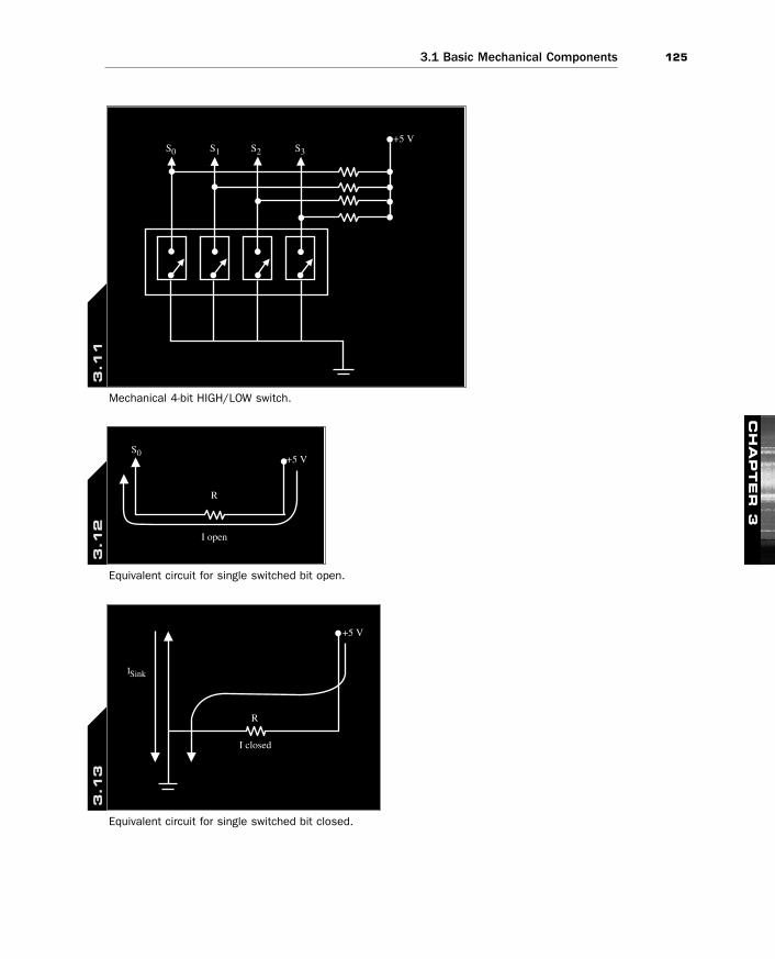
For example, say that we need 4 control lines to either be 0 or 1; these controllines might select a memory chip or a port, who knows, but as a hardwaredesigner we want a way to use a switch to send four 0/1 signals. Figure 3.11 illus-trates a DIP4 circuit that does this. Referring to the circuit, there are 4 indepen-dent switch circuits, each tied to ground, and each has a resistor connecting it tothe system’s +5 power supply. All the switch circuits are identical, so we need only
04_0672328208_ch03.qxd 11/15/05 2:47 PM Page 123

124 3.1 Basic Mechanical Components
analyze one such as S0. When S0 is open, there is a path from the +5 supply tothe output of S0, so any connection made to S0’s port will see a +5; this equiva-lent circuit is shown in Figure 3.12. A small current Iopen will flow in this case. Aslong as Iopen is very small (a few milliamps or microamps), the voltage drop overthe resistor will be small and the port at S0 will have nearly +5 volts on it (aHIGH or “1” in digital electronics). The amount of current that flows depends onthe resistor and the circuit that is being fed by the port. In most cases with TTL(transistor transistor logic), the load current will be milliamps, and with CMOS(Complementary Metal Oxide Semiconductor), the load current will be nearly 0 orin micro amps. The point being—the current Iopen is very small and we don’t needto worry too much about it. Now, the second case is more interesting; let’s look atthat.
CH
AP
TE
R 3
Images of DIP switches.
3.1
0
When the S0 switch is open, the port at S0 is feed with a +5 volt, but when weclose the switch then we “short” S0 to ground. What happens now? Referring toFigure 3.13, there is an equivalent circuit shown for this case. There are twocurrent branches, one from the +5 through the resistor to ground; this currentIclosed will always be
Iclosed = V/R = +5/R
04_0672328208_ch03.qxd 11/15/05 2:47 PM Page 124
1253.1 Basic Mechanical Components
CH
AP
TE
R 3
S1 S2 S3S0
+5 V
Mechanical 4-bit HIGH/LOW switch.
3.1
1
+5 V
I open
R
S0
Equivalent circuit for single switched bit open.
3.1
2
I Sink
+5 V
I closed
R
Equivalent circuit for single switched bit closed.
3.1
3
04_0672328208_ch03.qxd 11/15/05 2:47 PM Page 125

126 3.1 Basic Mechanical Components
Thus, this is one consideration when selecting R. The second current is the “sink”current needed by the device being driven to pull it down to a logic level 0; this isin the specification/data sheet and we will learn it later, but again might be a fewmicro to milliamps, but since we are shorting directly to ground, this current willalways be sinkable. Therefore, this switch with a passive resistor array creates a 4-bit 0/1 digital signal. The one confusing thing about the arrangement is thatwhen the switch is CLOSED or “ON,” the circuit creates a 0 (0V); when the switchis OPEN or “OFF” the circuit creates a 1 (+5V). This is simply the way that it isdesigned.
CH
AP
TE
R 3
You might be tempted to save the resistors and make the circuit work more intuitivelyby connecting each switch to +5. When the switch is on, there is a +5 or “1”; whenthe switch is off there is no signal, so a “0”—WRONG! When the switch is off, youhave no idea what is going to happen; this is like an uninitialized variable in C/C++.You must set the voltage yourself, otherwise the system will “float” to whatever. Infact, it might even work until someone waves their hand over the circuit and creates acapacitive coupling to ground! So always complete the design and make sure alldigital signals are set by you. We will get into this more later.
One last note: The configuration of resistors we just saw in the DIP switchexample is called “pull ups.” They are named that way since they pull-up thesignals. There are also pull-downs; you can pull signals down to ground as well ofcourse. However, most designers prefer pulling signals up rather than down, sincea digital “1” takes less current sometimes to generate than a digital “0”, so a pull-up and short to ground is cleaner.
3.1.1.4 Rotary Switches Rotary switches are used when you want to gate or send a signal from one (ormore) sources to one of N possible destinations (old TV sets used to have theserotary switches, for example). Figure 3.14 illustrates a one pole, N-way rotaryswitch. The single pole can be thought of as the “common” node (not necessarilyground), and by rotating the mechanical switch you can send the common signalto any one of the N-connections. Or you can use the switch backward and thinkof connecting one of the N-ways to the common. For example, when I was inhigh school, I made a little communications network with TVs and audio for theschool. They wanted to be able to send a TV signal and audio signal to one of 5rooms from a single source. Of course this is trivial with one of these switches;assuming a common system ground for example, I sent the composite videosignal to one of five rooms using a circuit as shown in Figure 3.15. A similarcircuit was used for audio. Of course, I put the whole circuit in a box, labeled itreally nice and added a 9V battery with some blinking lights to make it look likeit did something more complicated!
04_0672328208_ch03.qxd 11/15/05 2:47 PM Page 126

1273.1 Basic Mechanical Components
CH
AP
TE
R 3
A rotary switch.
3.1
4
Video In
Video RouterSwitch
Gnd
Gnd
Monitor Room 2
Monitor Room 4
Monitor Room 5
Monitor Room 3
Monitor Room 1
Room1
2
4
5
3
A video selector circuit based on a rotary switch.
3.1
5
04_0672328208_ch03.qxd 11/15/05 2:47 PM Page 127
128 3.1 Basic Mechanical Components
3.1.1.5 A Plethora of SwitchesAlthough the switches we just covered are the most commonly used, there are somany kinds of switches you could literally fill a 2,000 page book with them. Inother words, if you have a mechanical event that you want to detect with aswitch, there’s something; I guarantee it. Some examples of exotic switchingmechanisms are
Hall Effect switches that switch or detect magnetic fields.
Mercury switches that turn on/off based on orientation and a floating glob of conduc-tive mercury.
Reed switches that turn on/off based on the application of a magnetic field that effectsan internal permanent magnet inside the switch.
Pressure switches that turn on/off based on air pressure or vacuum.
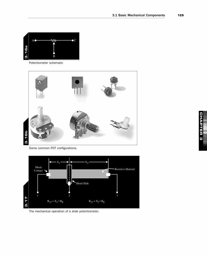
3.1.2 PotentiometersPotentiometers (POT) are nothing more than variable resistors. Figure 3.16 showsthe schematic symbol of one along with a few actual devices. Basically, there is aknob or slide on the potentiometer that allows you to adjust the resistance from 0to the maximum value. These are VERY useful devices. Internally, potentiometerswork more or less by having the port contacts 1,2,3 connected to a piece of resis-tive material like carbon. When the slide or knob is turned, the current pathlength through the resistive element is changed as shown in Figure 3.17. Since theresistance of any material increases proportionally to its length, by placing acontact at two ends of the resistive material (contacts 1 and 3) and then placing amovable contact that makes a frictional contact to the resistive element (contact2), you can change the resistance between contact 1 and 2 (call it R12) andbetween contacts 2 and 3 (call it R23) by moving the slide, knob, etc. Therefore,referring to Figure 3.17, the resistance of each branch or contact pair is simply
R12 = X1*Re
R23 = X2*Re
Or if the total resistance of the element is Rpot then
R12 = X1*Re
R23 = Rpot – R12
CH
AP
TE
R 3
04_0672328208_ch03.qxd 11/15/05 2:47 PM Page 128
1293.1 Basic Mechanical Components
CH
AP
TE
R 3
A
B
C
Potentiometer schematic
3.1
6a
Some common POT configurations.
3.1
6b
MetalContact
Metal Slide
Resistive Material
R12 = X1 • RE R23 = X2 • RE
1 2 3
X1 X2
The mechanical operation of a slide potentiometer.
3.1
7
04_0672328208_ch03.qxd 11/15/05 2:47 PM Page 129
130 3.1 Basic Mechanical Components
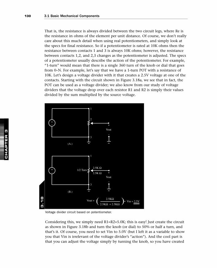
That is, the resistance is always divided between the two circuit legs, where Re isthe resistance in ohms of the element per unit distance. Of course, we don’t reallycare about this much detail when using real potentiometers, and simply look atthe specs for final resistance. So if a potentiometer is rated at 10K ohms then theresistance between contacts 1 and 3 is always 10K ohms; however, the resistancebetween contacts 1,2, and 2,3 changes as the potentiometer is adjusted. The specsof a potentiometer usually describe the action of the potentiometer. For example,“1-turn” would mean that there is a single 360 turn of the knob or dial that goesfrom 0–N. For example, let’s say that we have a 1-turn POT with a resistance of10K. Let’s design a voltage divider with it that creates a 2.5V voltage at one of thecontacts. Starting with the circuit shown in Figure 3.18a, we see that in fact, thePOT can be used as a voltage divider; we also know from our study of voltagedividers that the voltage drop over each resistor R1 and R2 is simply their valuesdivided by the sum multiplied by the source voltage.
CH
AP
TE
R 3
Vout
Vout = ( ((
1
2
(A.)
(B.)
3
+
–
Vout
+
–
1
2.5K Ω1/2 Turn
2.5KΩ
2.5KΩ + 2.5KΩ
2.5K Ω
3
• Vin = 2.5V
+–
+–
Voltage divider circuit based on potentiometer.
3.1
8
Considering this, we simply need R1=R2=5.0K; this is easy! Just create the circuitas shown in Figure 3.18b and turn the knob (or dial) to 50% or half a turn, andthat’s it. Of course, you need to set Vin to 5.0V (but I left it as a variable to showyou that Vin is irrelevant of the voltage divider’s “action”). And the cool part isthat you can adjust the voltage simply by turning the knob, so you have created
04_0672328208_ch03.qxd 11/15/05 2:47 PM Page 130

1313.2 Capacitor Circuits
an adjustable voltage supply. Of course, there’s the problem that you can onlypull very little current with the supply, since any load would alter the impedancetoo much. However, if you were to use say a 100 ohm POT for the adjustmentinstead of 10K ohm and then only attach loads that pulled a few milliamperes,you would be fine.
As a final note, potentiometers are mechanical and thus have a lifetime; you can’tturn them back and forth an infinite number of times. They are fine for adjust-ments, but if you used them to constantly change something they would wear outand break. Also, they are nothing more than resistors internally, and thus havemaximum power dissipation specifications in the watt range usually.
3.2 Capacitor CircuitsIn Chapter 1, we covered the physics and the mathematics behind capacitors forthe most part. In a nutshell, they are two metal plates separated by an insulator(air, paper, etc.). Capacitors are measured as farads C, and the governing equa-tions for capacitance is
Equation 3.1: Capacitance
I = C*dv/dt
This formula states that the current I, measured in amps, flowing in a capacitor isequal to the capacitance C measured in farads times the rate change of voltagemeasured in volts per second. Figure 3.19 shows the schematic symbols used forcapacitors and the current direction convention (+ to – is positive). Notice thatsome capacitors are polarized, others are bipolar or monolithic. Typically, polar-ized capacitors have much larger values than monolithic or bipolar types.Examples of polarized capacitors are
Electrolytics—Usually very bulky, very large values for capacitance. Cheap, highleakage, poor temperature stability. Used mostly for power supply filtering and de-coupling. Low frequency applications.
Tantalums—High values, more stable, low impedance, reasonable stability. Used for de-coupling and low to medium frequency applications. Very expensive.
CH
AP
TE
R 3
You must place polarized capacitors in your circuit the correct way or else they will bedamaged or may explode.
There are also non-polarized or bipolar capacitors, the most common of which areceramic or multilayer ceramic. These capacitors have good stability, are very highfrequency, and have low leakage. They are good for de-coupling and general-purpose medium-to-high-speed capacitors.
04_0672328208_ch03.qxd 11/15/05 2:47 PM Page 131

132 3.2 Capacitor Circuits
In most cases the capacitors you will use in any design will range from picofaradsto microfarads. I have never seen a capacitor larger than 200,000 microfarads,which is really 200 millifarads! That capacitor was about as big as a loaf of bread,so a 1 farad capacitor would be very large indeed.
In general, I suggest using electrolytics in the “dirty” parts of your design like inthe power supply input and filtering. Also, if you are AC coupling one circuit toanother (you will learn about this shortly), electrolytics will do; however, in audiocircuits they may not “sound” very good. That is, they have frequency-dependenteffects that may not be desirable. Tantalums are good where low lead impedanceand low internal ESR (equivalent series resistance) is needed and low leakage.
CH
AP
TE
R 3
Polarized
IC
(B.) Charging
Load
(C.) Discharging
(D.) Modeling Equations
•••
IC
(A.)
+C
+
–
–
Monolithic
Non–polarized
I dt = V(t1) – V(t0)
t1
t0
C
1
I dt = C dv
t1
t0 t0
t1
+C–
I = C dvdt
at t0 = 0
Initial Condition
V(t) = V(0) +
0
t
I dtC
1
Symbols/current conventions for charging and discharging along with modelingequations.
3.1
9
04_0672328208_ch03.qxd 11/15/05 2:47 PM Page 132

1333.2 Capacitor Circuits
Lastly, I suggest using the ceramics everywhere they will work: de-coupling, andin your general circuits. The only problem is they tend to come in small valuesand have high variance in their tolerance, but you can get 1–5% tolerance ceram-ics for more money.
CH
AP
TE
R 3
I have been showing you only “through hole” components thus far; of course there isa whole world of “surface mount” or SMT (surface mount technology) available, butthese are hard to build with, so I am not going to discuss them for the most part.However, SMT parts use more advanced technology and thus you can have a 10µfceramic capacitor in a grain of salt, so keep that in mind. When you make consumerdevice it will all be SMT, so many of these restrictions on size, etc. will go away.
Capacitors are used a number of ways in electronic circuits. In analog circuits,they have many uses and are the basis of many circuits, but in digital circuits theyhave uses as well, in power de-coupling and interfacing to the real world, forexample. But, at the end of the day a capacitor is an energy storage device—period. You charge the capacitor by applying a voltage, and it stores the chargeand then later can generate a voltage. The charging and discharging is exponen-tial, which you will see in a moment. Let’s take a look at the capacitor modelsagain and see some examples of how to use them.
3.2.1 Capacitor ModelsInternally a capacitor really has more than just capacitance; there is also a seriesresistance associated with the capacitor (ESR—equivalent series resistance) as wellas lead inductance and leakage. All are so small that in most cases you can forgetabout them unless it’s a high-precision design (voltage regulators for examplehave very specific needs for the capacitors, so beware). Considering this we canmodel a capacitor as a perfect model in most cases and just talk about the capaci-tance. So let’s see what a capacitor does in real circuits. First, starting with thecapacitor equation
I = C*dv/dt
This states that the current is the time derivative of the voltage. Another interest-ing result is if we integrate this function (those who don’t know calculus, just tryto follow; the results are all that matter).
I = C*dv/dt
Dividing by C, and multiplying both sides by dt
I/C * dt = dv
04_0672328208_ch03.qxd 11/15/05 2:47 PM Page 133

134 3.2 Capacitor Circuits
And now assuming that the circuit is operating for 0 to time t, we get
In other words, the voltage on a capacitor is the integral or sum of the currentover the time divided by the capacitance, an interesting side note. Astute readerswill realize that based on these results, capacitors (and their cousins inductors)can be used for analog computing and the computation of derivatives and inte-grals!
3.2.1.1 ChargingReferring to Figure 3.19, we have the most simplistic capacitor model: There is acurrent Ic that is flowing in the circuit that is charging the capacitor based on thegoverning capacitor equation. What actually happens is interesting. At somepoint the capacitor will fully charge to the voltage across it V; when this happensthe current Ic will be 0 by definition. Then the capacitor is fully charged and nocurrent will flow. Once the capacitor is charged then it is free to discharge(through a load); let’s see that. There is an interesting side effect of this chargingprocess, and that is that capacitors only pass AC, not DC currents. That is, the DCcurrent must be changing for there to be a current flow. This is apparent from thegoverning equation:
I = C*dv/dt
V(t) = V(0) + (1/C) * I * dt
t
0
CH
AP
TE
R 3
6v5v4v3v2v1v0v
6v5v4v3v2v1v0v
00Time (t)
(A.) AC + DC (B.) AC only
DC offset = 5 V
=> =>
Vol
tage
(V
)
Vol
tage
(V
)
C
+ –
Time (t)
AC only
Capacitors block DC.
3.2
0
The right side is 0 if the change in voltage per unit time is 0. But, the interpreta-tion of this is more subtle. The interpretation is that we can use capacitors toblock DC and pass AC. Figure 3.20 depicts this wonderful side effect. So using acapacitor we can strip away the DC component of a signal and simply obtain thechange or AC component. For example, say you had an audio signal that was5–6V as shown in Figure 3.20a, but your amplifier likes signals that vary from0–1V. You could use an AC coupling capacitor to strip the DC component and
04_0672328208_ch03.qxd 11/15/05 2:47 PM Page 134
1353.2 Capacitor Circuits
only pass that AC; this would result in a signal from 0–1V only (the AC compo-nent) as shown in Figure 3.20b. This configuration of a capacitor is actually a“filter,” and care needs to be taken in selecting the value of the capacitor since it’strue that all capacitors will block DC, but the value of the capacitor along withthe resistance or impedance of the circuit will also dictate the impedance of theAC component, so for frequencies we want to pass, we need to make sure thevalue C of the circuit is selected correctly to take this into consideration. However,the rule of thumb for audio applications is that a 1–10µF capacitor is going to passthe audio frequencies from 20Hz–20KHz just fine, while blocking the DC.
3.2.1.2 DischargingReferring to Figure 3.19c, we see the discharge of the capacitor. In this case, noticethat the current Ic changes direction from the charging case. This makes sensesince the capacitor is sourcing the current from the previous charge. The capacitorwill continue to discharge until the charge on its plates are depleted; at this pointthe voltage V will be zero as well as the current Ic=0.
3.2.2 Capacitors in Series and ParallelBefore moving on to RC circuits and putting everything together, let’s take amomentary detour to see how to add capacitors in series and parallel. The resultsbelow come directly from the definition of capacitance Q=CV, and the governingequation, I=C*dv/dt.
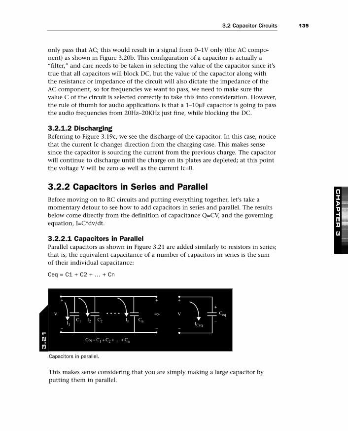
3.2.2.1 Capacitors in ParallelParallel capacitors as shown in Figure 3.21 are added similarly to resistors in series;that is, the equivalent capacitance of a number of capacitors in series is the sumof their individual capacitance:
Ceq = C1 + C2 + … + Cn
CH
AP
TE
R 3
C1
+
–
+
–
+
–
+
–C2
• • • •Cn
Ceq
ICeq
=>
Ceq = C1 + C2 + … + Cn
I2I1
V VIn
Capacitors in parallel.
3.2
1
This makes sense considering that you are simply making a large capacitor byputting them in parallel.
04_0672328208_ch03.qxd 11/15/05 2:47 PM Page 135

136 3.2 Capacitor Circuits
3.2.2.2 Capacitors in SeriesCapacitance in series is a little more complex to derive, but the results are thesame as resistors in parallel (big surprise):
1/Ceq = 1/C1 + 1/C2 + … + 1/Cn
Which for two capacitors in series as shown in Figure 3.22 simplifies to
Ceq = (C1*C2) / (C1+C2)
CH
AP
TE
R 3
When placing capacitors in parallel, make sure that they are all placed with thecorrect polarity if polarized; also make sure they can handle the maximum voltagebeing applied. One of the specs for a capacitor is the maximum voltage that can beapplied, usually anywhere from a few volts to a few hundred, with your typical designcapacitors in the 25–50V range. However, as a rule I always overdesign by a factor of100%, so if my design needs a capacitor to charge to 25V, I am sure to use a 50Vcapacitor. Even if the capacitor will never see that voltage, running it at a max of 50%its tolerated voltage will increase its lifespan, and 30 years from now when you fireup some game console you design it will work just like the Apple II, Atari 800, andC64 do!
C1
+
–
– – +
–C2 C3 Cn
Ceq+ + –+ –+
• • • •I
=> V
1
Ceq =
C1 +
C2 +
• +
Cn
1 1 1
Capacitors in series.
3.2
2
Now, you should have a picture of what happens during charging and discharg-ing, along with how to compute series and parallel capacitor arrays. Let’s build amore formal circuit with some components and model the system, so we can atleast see how to create some basic capacitor circuits.
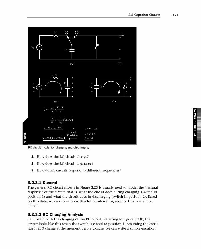
3.2.3 RC CircuitsRC circuits simply refer to any circuit that has resistive and capacitive elements.Since we know how to find both the equivalent resistance of resistors in anetwork and the equivalent capacitance of capacitors in a network, we can focuson a simplified model of an RC circuit as shown in Figure 3.23. We want toanalyze this circuit and answer some basic questions:
04_0672328208_ch03.qxd 11/15/05 2:47 PM Page 136
1373.2 Capacitor Circuits
1. How does the RC circuit charge?
2. How does the RC circuit discharge?
3. How do RC circuits respond to different frequencies?
3.2.3.1 GeneralThe general RC circuit shown in Figure 3.23 is usually used to model the “naturalresponse” of the circuit; that is, what the circuit does during charging (switch inposition 1) and what the circuit does in discharging (switch in position 2). Basedon this data, we can come up with a lot of interesting uses for this very simplecircuit.
3.2.3.2 RC Charging AnalysisLet’s begin with the charging of the RC circuit. Referring to Figure 3.23b, thecircuit looks like this when the switch is closed to position 1. Assuming the capac-itor is at 0 charge at the moment before closure, we can write a simple equation
CH
AP
TE
R 3
+++
+
––
–
–
VVI
+
–
V
+
–
VI
V0
VI
R
=> V = Vi + Ae – t/RC
V = Vi (1 – e – t/RC)
0 = Vi + Ae0
A = –Vi
InitialConditions 0 = Vi + A
R
R
R1
C
C
C
(C.)(B.)
(A.)
+–
+
+
–
( (Vi – V =dvdt
1RC
VI – V
RIc = C =
dvdt
1 2
RC circuit model for charging and discharging.
3.2
3
04_0672328208_ch03.qxd 11/15/05 2:47 PM Page 137
138 3.2 Capacitor Circuits
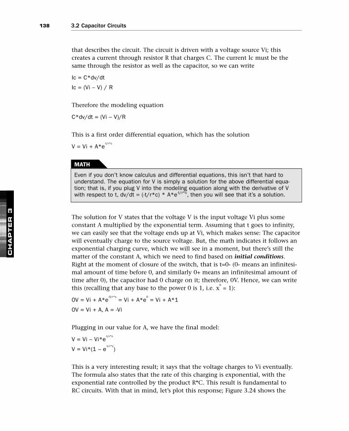
that describes the circuit. The circuit is driven with a voltage source Vi; thiscreates a current through resistor R that charges C. The current Ic must be thesame through the resistor as well as the capacitor, so we can write
Ic = C*dv/dt
Ic = (Vi – V) / R
Therefore the modeling equation
C*dv/dt = (Vi – V)/R
This is a first order differential equation, which has the solution
V = Vi + A*e-t/r*c
CH
AP
TE
R 3
MATH
Even if you don’t know calculus and differential equations, this isn’t that hard tounderstand. The equation for V is simply a solution for the above differential equa-tion; that is, if you plug V into the modeling equation along with the derivative of Vwith respect to t, dv/dt = (-t/r*c) * A*e-t/r*c, then you will see that it’s a solution.
The solution for V states that the voltage V is the input voltage Vi plus someconstant A multiplied by the exponential term. Assuming that t goes to infinity,we can easily see that the voltage ends up at Vi, which makes sense: The capacitorwill eventually charge to the source voltage. But, the math indicates it follows anexponential charging curve, which we will see in a moment, but there’s still thematter of the constant A, which we need to find based on initial conditions.Right at the moment of closure of the switch, that is t=0- (0- means an infinitesi-mal amount of time before 0, and similarly 0+ means an infinitesimal amount oftime after 0), the capacitor had 0 charge on it; therefore, 0V. Hence, we can writethis (recalling that any base to the power 0 is 1, i.e. x
0= 1):
0V = Vi + A*e-0/r*c
= Vi + A*e0
= Vi + A*1
0V = Vi + A, A = -Vi
Plugging in our value for A, we have the final model:
V = Vi – Vi*e-t/r*c
V = Vi*(1 – e-t/r*c
)
This is a very interesting result; it says that the voltage charges to Vi eventually.The formula also states that the rate of this charging is exponential, with theexponential rate controlled by the product R*C. This result is fundamental to RC circuits. With that in mind, let’s plot this response; Figure 3.24 shows the
04_0672328208_ch03.qxd 11/15/05 2:47 PM Page 138
1393.2 Capacitor Circuits
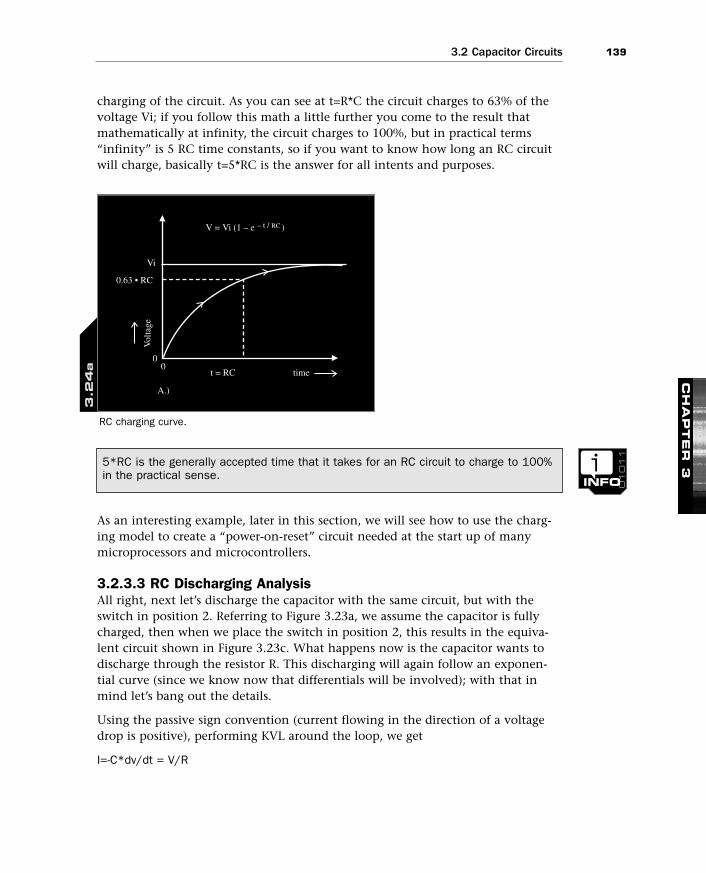
charging of the circuit. As you can see at t=R*C the circuit charges to 63% of thevoltage Vi; if you follow this math a little further you come to the result thatmathematically at infinity, the circuit charges to 100%, but in practical terms“infinity” is 5 RC time constants, so if you want to know how long an RC circuitwill charge, basically t=5*RC is the answer for all intents and purposes.
CH
AP
TE
R 3
0.63 • RC
A.)
Vi
timet = RC
Vol
tage
V = Vi (1 – e – t / RC )
00
RC charging curve.
3.2
4a
As an interesting example, later in this section, we will see how to use the charg-ing model to create a “power-on-reset” circuit needed at the start up of manymicroprocessors and microcontrollers.
3.2.3.3 RC Discharging AnalysisAll right, next let’s discharge the capacitor with the same circuit, but with theswitch in position 2. Referring to Figure 3.23a, we assume the capacitor is fullycharged, then when we place the switch in position 2, this results in the equiva-lent circuit shown in Figure 3.23c. What happens now is the capacitor wants todischarge through the resistor R. This discharging will again follow an exponen-tial curve (since we know now that differentials will be involved); with that inmind let’s bang out the details.
Using the passive sign convention (current flowing in the direction of a voltagedrop is positive), performing KVL around the loop, we get
I=-C*dv/dt = V/R
5*RC is the generally accepted time that it takes for an RC circuit to charge to 100%in the practical sense.
04_0672328208_ch03.qxd 11/15/05 2:47 PM Page 139

140 3.2 Capacitor Circuits
The solution to this is an exponential of the form
V = A*e-t/r*c
Plugging in V=Vi at t=0, we get the value of the constant for the final result of
V = Vi*e-t/r*c
CH
AP
TE
R 3
B.)
t = RC
ViI
Vi
time
RC
V (t) = Vi • e – t / RC
V = Vi • e – t / RC
Vol
tage
+ +
– –
I = VR
00
– C • dv V I = = dt R
RC discharging curve.
3.2
4b
Which should make sense. And for fun, let’s graph this result as shown in Figure3.24b. As you can see, it’s similar to the graph for the charging, but inverted. Also,at t=RC the system has discharged to 37% of its initial charge; this is easy to seeusing the discharge formula:
V = Vi*e-r*c/r*c
= Vi*e-1
= Vi*(0.367)
That is, V = 36% of Vi at t=RC.
Now that you have charging and discharging under you belt, let’s see some veryuseful circuits we can construct with these results.
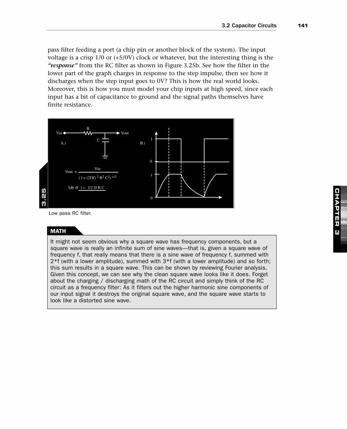
3.2.4 Low Pass FiltersThe previous RC circuit we analyzed was actually a low pass filter. This meansthat the circuit tends to pass low frequency signals and send to ground highfrequency signals. Referring to Figure 3.25a, we see a real-world example of a low
04_0672328208_ch03.qxd 11/15/05 2:47 PM Page 140
1413.2 Capacitor Circuits
pass filter feeding a port (a chip pin or another block of the system). The inputvoltage is a crisp 1/0 or (+5/0V) clock or whatever, but the interesting thing is the“response” from the RC filter as shown in Figure 3.25b. See how the filter in thelower part of the graph charges in response to the step impulse, then see how itdischarges when the step input goes to 0V? This is how the real world looks.Moreover, this is how you must model your chip inputs at high speed, since eachinput has a bit of capacitance to ground and the signal paths themselves havefinite resistance.
CH
AP
TE
R 3
A.) B.)C
R
1
1( l + (2Πf) 2 R2 C2) 1/2
0
0
3db @ f = 1/2 Π R C
Vout =Vin
VoutVin
Low pass RC filter.
3.2
5
MATH
It might not seem obvious why a square wave has frequency components, but asquare wave is really an infinite sum of sine waves—that is, given a square wave offrequency f, that really means that there is a sine wave of frequency f, summed with2*f (with a lower amplitude), summed with 3*f (with a lower amplitude) and so forth;this sum results in a square wave. This can be shown by reviewing Fourier analysis.Given this concept, we can see why the clean square wave looks like it does. Forgetabout the charging / discharging math of the RC circuit and simply think of the RCcircuit as a frequency filter: As it filters out the higher harmonic sine components ofour input signal it destroys the original square wave, and the square wave starts tolook like a distorted sine wave.
04_0672328208_ch03.qxd 11/15/05 2:47 PM Page 141
142 3.2 Capacitor Circuits
If we forget about the “time domain” that we have been working in for amoment and talk about the “frequency domain,” then we can be more specificabout frequency related effects of the low pass filter. All the frequency domainmeans is that we discuss signals in terms of their frequency rather than their timevarying descriptions; in filter analysis this is much more productive. If we let thefrequency of the signal be f, then the gain of the low pass filter or the ratio of theoutput to the input is
Low Pass Gain
Vout/Vin = 1/[1+(2*∏*f)2*R
2*C
2]1/2
Or
Vout/Vin = 1/[1+(f3dB)2*R
2*C
2]1/2
where f3dB = 1/2*∏*R*C
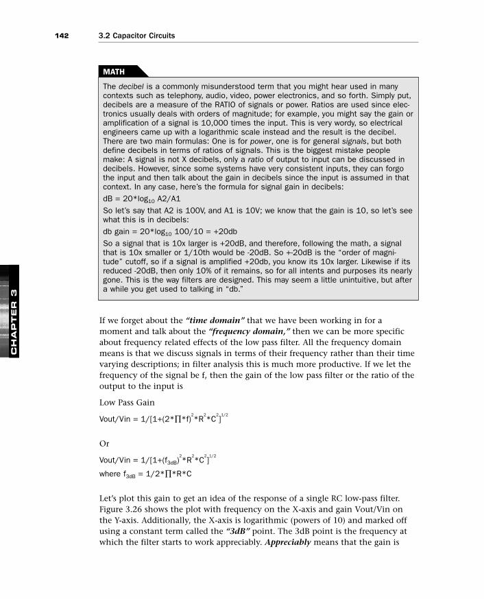
Let’s plot this gain to get an idea of the response of a single RC low-pass filter.Figure 3.26 shows the plot with frequency on the X-axis and gain Vout/Vin onthe Y-axis. Additionally, the X-axis is logarithmic (powers of 10) and marked offusing a constant term called the “3dB” point. The 3dB point is the frequency atwhich the filter starts to work appreciably. Appreciably means that the gain is
CH
AP
TE
R 3
MATH
The decibel is a commonly misunderstood term that you might hear used in manycontexts such as telephony, audio, video, power electronics, and so forth. Simply put,decibels are a measure of the RATIO of signals or power. Ratios are used since elec-tronics usually deals with orders of magnitude; for example, you might say the gain oramplification of a signal is 10,000 times the input. This is very wordy, so electricalengineers came up with a logarithmic scale instead and the result is the decibel.There are two main formulas: One is for power, one is for general signals, but bothdefine decibels in terms of ratios of signals. This is the biggest mistake peoplemake: A signal is not X decibels, only a ratio of output to input can be discussed indecibels. However, since some systems have very consistent inputs, they can forgothe input and then talk about the gain in decibels since the input is assumed in thatcontext. In any case, here’s the formula for signal gain in decibels:dB = 20*log10 A2/A1So let’s say that A2 is 100V, and A1 is 10V; we know that the gain is 10, so let’s seewhat this is in decibels:db gain = 20*log10 100/10 = +20dbSo a signal that is 10x larger is +20dB, and therefore, following the math, a signalthat is 10x smaller or 1/10th would be -20dB. So +-20dB is the “order of magni-tude” cutoff, so if a signal is amplified +20db, you know its 10x larger. Likewise if itsreduced -20dB, then only 10% of it remains, so for all intents and purposes its nearlygone. This is the way filters are designed. This may seem a little unintuitive, but aftera while you get used to talking in “db.”
04_0672328208_ch03.qxd 11/15/05 2:47 PM Page 142
1433.2 Capacitor Circuits
about 70% roughly or .707, so when the filter kicks in we like to call this the 3dBpoint and use it as a reference. In this case, considering this, it’s easy to under-stand the frequency/gain graph in Figure 3.26. At f = 0, the gain of the system is1.0; as we increase the frequency in powers of 10 times the frequency of the 3dBmark, we see the filter start working. For example, at f3dB the gain is .707 (so thefrequencies at f=1/2*∏*R*C will be impeded and only .707 will get through), butat 10*f3dB the gain is nearly down to 0.1 and the filter is really starting to filter thesignal, and at 100*f3dB there is nothing getting through.
CH
AP
TE
R 3
0.707
1.0
0.01*3db 0.1*3db 10*3db 100*3dbf = 2ΠRC
“3db” point
3 = 20 Log x
x = e 3/20
0
Gain Slope = –20db/ decade
f
Low pass RC filter response curve.
3.2
6
So that’s all there is to the low-pass filter! For example, say you wanted to filter asignal at 10KHz: You want to pass 10KHz, but start filtering after that. We simplyuse 10KHz as the f3dB point and make an RC filter. Based on the equation f3dB =2*∏*R*C, and assuming we have lots of 1K resistors lying around, we get
10KHz = 1/2*∏*1K*C
C = 1/2*∏*1K*10Khz = .0159µF
So, we might use a 0.01µF capacitor since it’s a common value; of course this willshift the f3dB point slighty, but probably not enough to make a difference to us. Asa last note, realize that the filtering of single RC stage occurs at -20dB per decade.If you want a “brick wall” that falls off faster you must cascade stages of RC filters;each stage will give you another -20dB of fall off. However, in our case whendesigning embedded systems and video game consoles, a single stage low-passfilter is about as complicated as it gets.
04_0672328208_ch03.qxd 11/15/05 2:47 PM Page 143

144 3.2 Capacitor Circuits
3.2.5 High pass FiltersHigh pass filters are nearly identical to low pass filters except they pass highfrequencies rather than low. And amazingly all you do is swap the R and C in alow pass filter and now you have a high pass filter, as shown in Figure 3.27. Themath is left as an exercise; the results for high-pass gain are
Vout/Vin = R /[ R2 + 1/((2*∏*f)
2*C
2)]
1/2
Or another form is
Vout/Vin = 2*∏*f*R*C /[ 1 + 1/((2*∏*f)2)]
1/2
CH
AP
TE
R 3
[ 1 + (2 Π f RC) ] 1/2
R
“Transfer Function”
+ +
=
Vin (t)H (t) = Vout (t)
[ R2 + (1/ (2 Πf )2 (C2 )) ] 1/2
R
VinVout
=
2 Π f RC
C
Vin Vout
– –
High pass RC filter.
3.2
7
Again, the f3dB point is equal to 1/2*∏*R*C, and instead of this being where thefilter starts blocking the frequencies appreciably, this is where the high pass filtersstart passing them, thus the frequency versus gain graph looks like Figure 3.28.
3.2.6 POR—Power On Reset CircuitsWhen you power on your embedded system, most microprocessors and microcon-trollers have a reset line that must be pulled low or high for a good amount oftime (a few milliseconds at least); this is shown in Figure 3.29. Once the system ispowered up and the voltage supplies are stable (+5V, +3.3V, etc.), the system needsto issue a reset to the processor and peripherals. These reset circuits are tradition-ally called power-on-reset or POR circuits. In most cases, you can do this with asimple capacitor and resistor along with a reset switch. As an example, assumethat we have a processor (and system) that requires an active low (0V) reset signal;
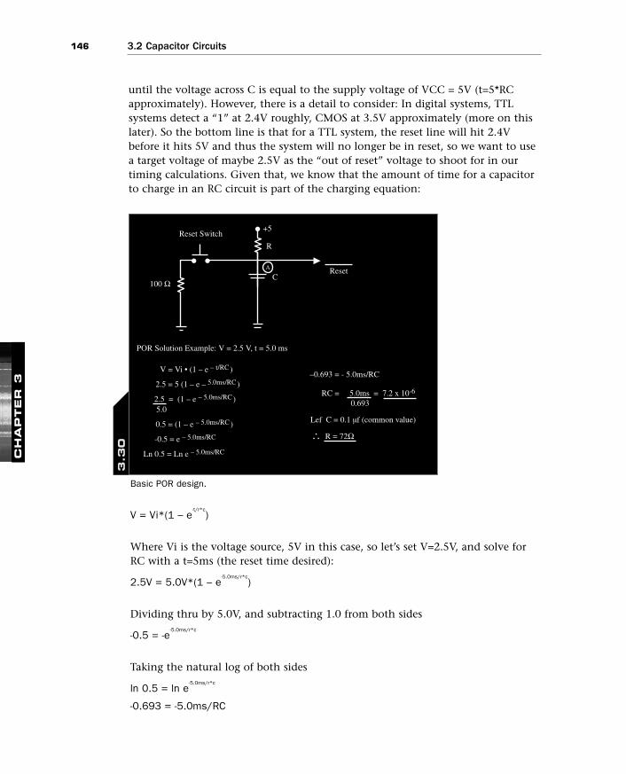
04_0672328208_ch03.qxd 11/15/05 2:47 PM Page 144

1453.2 Capacitor Circuits
3.2.6.1 POR AnalysisAssuming the system is unpowered and the reset button is not depressed, let’sapply power to the system at t=0. When we do this, the VCC line goes to +5V andthe RC circuit starts charging. However, at this point, the voltage at node A is 0Vapproximately, so the processor is being fed the required 0V reset signal. As theRC circuit charges the capacitor C, the voltage at the node will continue to rise,
CH
AP
TE
R 3
1.0Gain
0.707Vin
Vout
decade
20db
f3db = 12ΠRC
0
High pass RC filter response curve.
3.2
8we need to design a circuit that generates a low (0V) for a few milliseconds, butthen changes to +5V at some point. Let’s also assume that the reset must exist for3.5ms, so let’s round to 5ms to be safe, and we want to give the user the ability tomanually reset the system with a push button. Figure 3.30 shows the design forsuch a system.
“Power Lines”“Power Good”
Reset
Reset
Microcomputer (µP)
Reset Line
t2 – t1 > min Reset time 5 – 50 ms
0 V
+5 V
t = 0 t = t1 t = t2
_
Powering up with reset.
3.2
9
04_0672328208_ch03.qxd 11/15/05 2:47 PM Page 145
146 3.2 Capacitor Circuits
until the voltage across C is equal to the supply voltage of VCC = 5V (t=5*RCapproximately). However, there is a detail to consider: In digital systems, TTLsystems detect a “1” at 2.4V roughly, CMOS at 3.5V approximately (more on thislater). So the bottom line is that for a TTL system, the reset line will hit 2.4Vbefore it hits 5V and thus the system will no longer be in reset, so we want to usea target voltage of maybe 2.5V as the “out of reset” voltage to shoot for in ourtiming calculations. Given that, we know that the amount of time for a capacitorto charge in an RC circuit is part of the charging equation:
CH
AP
TE
R 3
POR Solution Example: V = 2.5 V, t = 5.0 ms
100 ΩReset
C
R
+5Reset Switch
V = Vi • (1 – e – t/RC)
2.5 = 5 (1 – e – 5.0ms/RC)
0.5 = (1 – e – 5.0ms/RC) Lef C = 0.1 µf (common value)
–0.693 = - 5.0ms/RC
-0.5 = e – 5.0ms/RC
Ln 0.5 = Ln e – 5.0ms/RC
• •• R = 72Ω
RC = 5.0ms = 7.2 x 10⁻⁶
0.693
A
5.02.5 = (1 – e – 5.0ms/RC)
Basic POR design.
3.3
0
V = Vi*(1 – e-t/r*c
)
Where Vi is the voltage source, 5V in this case, so let’s set V=2.5V, and solve forRC with a t=5ms (the reset time desired):
2.5V = 5.0V*(1 – e-5.0ms/r*c
)
Dividing thru by 5.0V, and subtracting 1.0 from both sides
-0.5 = -e-5.0ms/r*c
Taking the natural log of both sides
ln 0.5 = ln e-5.0ms/r*c
-0.693 = -5.0ms/RC
04_0672328208_ch03.qxd 11/15/05 2:47 PM Page 146

1473.2 Capacitor Circuits
Solving for RC
RC = 7.2x10⁻⁶
Now, we have two unknowns and only one equation, so we have freedom to pickone as we wish. Let’s select a common value for C, and see what result we get forR. What about .1µF for C:
R = 7.2x10⁻⁶
/ 1µF = 72Ω
Since 72 ohms is hard to find, a value of 100 ohms will work, and the only effectwill be a slightly longer reset, which is fine.
CH
AP
TE
R 3
100 Ω
100 Ω
Reset
Reset
0.1 µF
+5V
Final POR design.
3.3
1
The final reset circuit is shown in Figure 3.31. The only thing left to discuss is themanual reset button. When this is depressed what happens? If the capacitor ischarged then it will immediately discharge through the 100 switch branch resistorto ground (this will take about 5ms as well), then the reset line will have a 0V onit until the user releases the reset button. When he does so, the circuit willrecharge in 5ms and take the machine out of reset once again. So the resistor inthe reset switch branch is needed to give the capacitor a discharge path with resis-tance; without it, the instantaneous current generated from the capacitor wouldbe huge. Also, last note, what about the tolerance and voltage rating of the capac-itor in our reset circuit? First, the tolerance isn’t that important; if we get theworst capacitor possibly it will range ±20%; this will mean ±1ms more or less resettime, which should be fine since we over designed the spec to 5ms to make sure.Lastly, the largest voltage on the capacitor should be 5V, so if we pick a nice15–25V capacitor our design should have a very long lifespan.
04_0672328208_ch03.qxd 11/15/05 2:47 PM Page 147
148 3.2 Capacitor Circuits
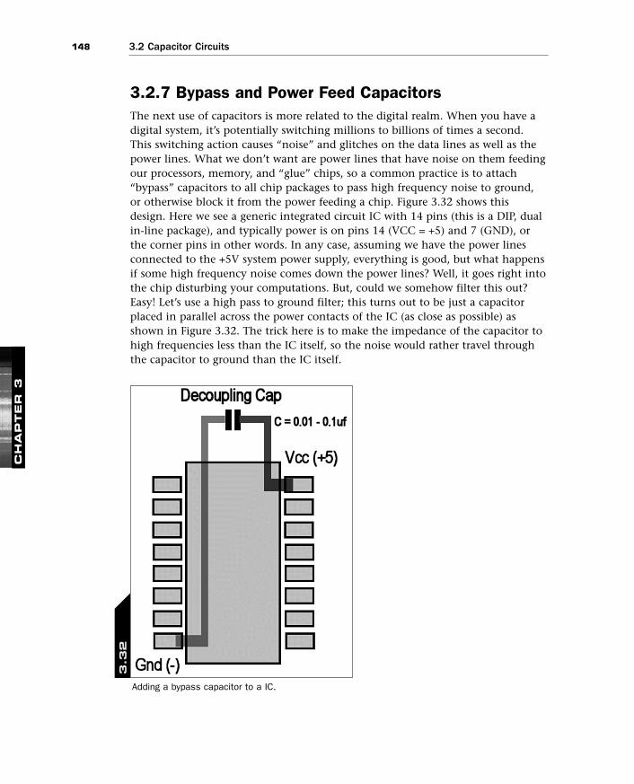
3.2.7 Bypass and Power Feed CapacitorsThe next use of capacitors is more related to the digital realm. When you have adigital system, it’s potentially switching millions to billions of times a second.This switching action causes “noise” and glitches on the data lines as well as thepower lines. What we don’t want are power lines that have noise on them feedingour processors, memory, and “glue” chips, so a common practice is to attach“bypass” capacitors to all chip packages to pass high frequency noise to ground,or otherwise block it from the power feeding a chip. Figure 3.32 shows thisdesign. Here we see a generic integrated circuit IC with 14 pins (this is a DIP, dualin-line package), and typically power is on pins 14 (VCC = +5) and 7 (GND), orthe corner pins in other words. In any case, assuming we have the power linesconnected to the +5V system power supply, everything is good, but what happensif some high frequency noise comes down the power lines? Well, it goes right intothe chip disturbing your computations. But, could we somehow filter this out?Easy! Let’s use a high pass to ground filter; this turns out to be just a capacitorplaced in parallel across the power contacts of the IC (as close as possible) asshown in Figure 3.32. The trick here is to make the impedance of the capacitor tohigh frequencies less than the IC itself, so the noise would rather travel throughthe capacitor to ground than the IC itself.
CH
AP
TE
R 3
Adding a bypass capacitor to a IC.
3.3
2
04_0672328208_ch03.qxd 11/15/05 2:47 PM Page 148

1493.2 Capacitor Circuits
Also, as you design faster and faster boards, the technique of bypassing individualchips no longer works as well, and you must distribute your bypass caps all overthe board in a matrix as shown in Figure 3.33. The values start to not even mattersince the lead inductance starts to dominate and thus your goal is simply to put alot of bypass caps on your board, equally spaced. However, for all our designs, justuse a 0.01µF–0.1µF for each IC and you will be fine. Additionally, for large ICsthat have busses, add a 1.0–10.0µF tantalum cap for power feeding. Why this isneeded can be explained with an example: Say you have an IC that is controllinga 32-bit bus. That bus changes state from digital 0 to 1 or vice versa; this generatesa huge current which will have to be fed or sunk by the power supply rails.However, those rails go all the way back to the power distribution network andthe power supply. That’s a long way for the current to travel with a lot of resis-tance, so what happens is that you get a huge voltage drop over your power linesand the voltage on your IC actually changes!
CH
AP
TE
R 3
Some rules of thumb: If your circuit is running from 1–10MHz then use .01µF–.1µFcaps to bypass each IC with; if your circuit is running from 10–100MHz then 100pFto .01µF capacitors will do. The bypass capacitors should be monolithic (non-polar-ized), 50V tolerant, and ceramic. Keep them as close as possible to the powercontacts of each IC.
Bypass capacitors distributed in a matrix.
3.3
3
This whole process can be understood by realizing that the ground the IC seestranslates up to maybe a few hundred millivolts—.2V or something—this can
04_0672328208_ch03.qxd 11/15/05 2:47 PM Page 149

150 3.2 Capacitor Circuits
cause problems, but by having a fat cap to feed the IC when this happens withvery short leads, it’s like having a power supply right on chip that can handleshort bursts of power. Thus your ground voltage won’t jump, so on all processors,memory, and large bus buffering chips, place a 1.0–10.0µF tantalum (low leadimpedance) and your design will be very clean.
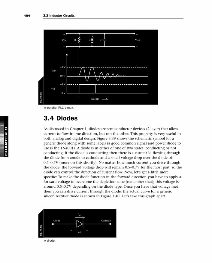
3.3 Inductor Circuits Inductors as discussed in Chapter 1, “Introduction to Electronics, Electrons, andLight Speed,” simply store energy in a magnetic field. In embedded system design,you won’t actually use many inductors; they are more commonly found in audioand video circuits or when designing complex filters. So, we don’t need to coverthem as in depth as we did with capacitors, so I just want to show you a couplecircuits and some results.
3.3.1 Inductors ModelFigure 3.34 depicts both a more physical image of an inductor and a circuitdiagram. To refresh your memory, the inductor works simply by passing a currentthrough the inductor: As the current flows, a magnetic field is generated. Thisfield strength is proportional to the number of turns of wire in the inductor, thegeometry, etc.; these factors are lumped together and called inductance, L, andmeasured in henrys, named after the physicist Joseph Henry. In any case, as thecurrent flows and the field is generated, this also develops a voltage across theinductor with the governing equation:
CH
AP
TE
R 3
+
+
Flux
VV L
I
I
di
dtV = L
–
–
Physical inductor model.
3.3
4
Equation 3.2: Inductance.
V = L*di/dt
04_0672328208_ch03.qxd 11/15/05 2:47 PM Page 150
1513.3 Inductor Circuits
That is, the rate change of current I in the circuit multiplied by the inductance isequal to the voltage, so 1 henry of inductance with 1 amp of current generates avoltage of 1V.
Inductors can be used just as capacitors to create low pass and high pass filters,but they would be huge in such cases. Therefore, as mentioned, inductors are onlyused in high frequency applications in most cases.
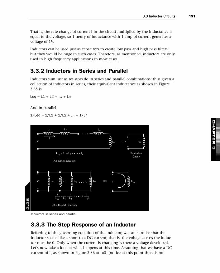
3.3.2 Inductors in Series and ParallelInductors sum just as resistors do in series and parallel combinations; thus given acollection of inductors in series, their equivalent inductance as shown in Figure3.35 is
Leq = L1 + L2 + … + Ln
And in parallel
1/Leq = 1/L1 + 1/L2 + … + 1/Ln
CH
AP
TE
R 3
V V
VI
L1 L2
L2L1 L3
L
L
Ln
I
EquivalentCircuit
=>
=>
(A.) Series Inductors
(B.) Parallel Inductors
–
– –
–
+ +
+ +
L1 L2 L1 1 1 1
Leq
Leq
Leq
Leq
= L1 + L2 + • • • + Ln
n
n
n• • • •
• • •
= + + +• • •
Inductors in series and parallel.
3.3
5
3.3.3 The Step Response of an InductorReferring to the governing equation of the inductor, we can surmise that theinductor seems like a short to a DC current; that is, the voltage across the induc-tor must be 0. Only when the current is changing is there a voltage developed.Let’s now take a look at what happens at this time. Assuming that we have a DCcurrent of I0 as shown in Figure 3.36 at t=0- (notice at this point there is no
04_0672328208_ch03.qxd 11/15/05 2:47 PM Page 151

152 3.3 Inductor Circuits
voltage drop over the inductor since it’s a short to the current source), we switchthe switch from position 1 to 2 and switch out the current source and switch inthe load resistor R; we now have the circuit shown in Figure 3.36. Writing a loopequation, we get
L*di/dt + R*I = 0
CH
AP
TE
R 3
L
V
V
t = 0 +
t = 0 +t = 0 –
RL
R
I
=>
I0
1 2
+
+
+
––
–
I
Inductor Analysis Circuit.
3.3
6
Which again is a first order differential equation with solution of the form A*ex;
knowing that and knowing that the current at t=0 is I0, we arrive at this finalsolution as a function of time t
I(t) = I0*e-(R/L)*t
Notice the (R/L) term? This is similar to the R*C term in the capacitor model, thusR/L is the time constant in an inductive circuit. These are all the results we needfor now; we aren’t going to use inductors in our designs, so it’s not worth thetime to pursue more analysis. Let’s take a look at some final results.
3.3.4 RLC CircuitsThe final model of many circuit elements, including conductor paths and filters,is a combination of R, L, and C. There are a number of possible permutations ofRLC, but let’s look at the two most obvious: series and parallel.
04_0672328208_ch03.qxd 11/15/05 2:47 PM Page 152

1533.3 Inductor Circuits
3.3.4.1 Series RLCFigure 3.37 depicts the step response of an RLC circuit to a digital 5V pulse. This isvery close to the real world and if you understand this you are 99% there tounderstanding what happens at the analog level of digital signals. In any case,referring to the figure, we send a digital signal through a transmission line—maybe it’s a data bus line, a control signal, etc.—in any case, due to the capaci-tance, inductance, and resistance of the connection, the line seems like a seriesRLC model, so what does the step function end up looking like? Figure 3.37 alsoshows this: We see that the signal rises exponentially as we suspected, but then it“rings” about the max; then when the step signal goes back to 0V, the RLC signalsfalls again to 0V exponentially, but rings again about 0V. So the inductance lookslike its causing this ringing effect, and it is, thus, you must keep the inductance ofyour lines small, otherwise you will ring them so much that the data may getcorrupted.
CH
AP
TE
R 3
L
+5
+5
0
R
C Vout
Vout
time (t) Step Input
Filtered Output
Vin
Vin
+ +
– –
A series RLC circuit.
3.3
7
3.3.4.2 Parallel RLCOkay, so that’s the first case, series RLC. Let’s take a look at a more interestingcase: parallel RLC, as shown in Figure 3.38. When you have a resistor, capacitor,and inductor in parallel like that, you create a special kind of circuit called an RL-tank—basically the precursor to an oscillator—so when you excite the circuit witha step input, the circuit charges and then discharges slowly by oscillating theenergy away. This is easy to understand if you think about the two energy storageelements (capacitor and inductor) feeding each other. So the bottom line is that ifyou place an RLC in parallel you might get oscillations! And if you didn’t intendthat you would have serious trouble.
04_0672328208_ch03.qxd 11/15/05 2:47 PM Page 153
154 3.3 Inductor Circuits
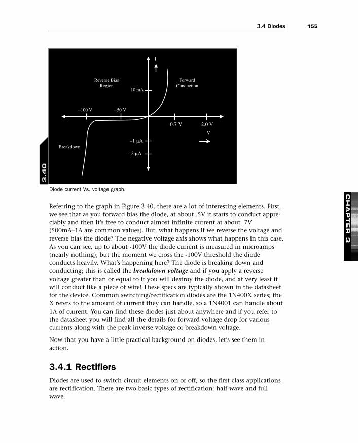
3.4 DiodesAs discussed in Chapter 1, diodes are semiconductor devices (2 layer) that allowcurrent to flow in one direction, but not the other. This property is very useful inboth analog and digital design. Figure 3.39 shows the schematic symbol for ageneric diode along with some labels (a good common signal and power diode touse is the 1N4001). A diode is in either of one of two states: conducting or notconducting. If the diode is conducting then there is a current Id flowing throughthe diode from anode to cathode and a small voltage drop over the diode of0.5–0.7V (more on this shortly). No matter how much current you drive throughthe diode, the forward voltage drop will remain 0.5–0.7V for the most part, so thediode can control the direction of current flow. Now, let’s get a little morespecific: To make the diode function in the forward direction you have to apply aforward voltage to overcome the depletion zone (remember that); this voltage isaround 0.5–0.7V depending on the diode type. Once you have that voltage metthen you can drive current through the diode; the actual curve for a genericsilicon rectifier diode is shown in Figure 3.40. Let’s take this graph apart.
CH
AP
TE
R 3
L CR
Vout
Vout
Vin
V in
+ +
– –
+5 V
+5 V
+0 V
0 V
time (t)
A parallel RLC circuit.
3.3
8
Vd
Anode Cathode
+ –
Id
A diode.
3.3
9
04_0672328208_ch03.qxd 11/15/05 2:47 PM Page 154
1553.4 Diodes
Referring to the graph in Figure 3.40, there are a lot of interesting elements. First,we see that as you forward bias the diode, at about .5V it starts to conduct appre-ciably and then it’s free to conduct almost infinite current at about .7V(500mA–1A are common values). But, what happens if we reverse the voltage andreverse bias the diode? The negative voltage axis shows what happens in this case.As you can see, up to about -100V the diode current is measured in microamps(nearly nothing), but the moment we cross the -100V threshold the diodeconducts heavily. What’s happening here? The diode is breaking down andconducting; this is called the breakdown voltage and if you apply a reversevoltage greater than or equal to it you will destroy the diode, and at very least itwill conduct like a piece of wire! These specs are typically shown in the datasheetfor the device. Common switching/rectification diodes are the 1N400X series; theX refers to the amount of current they can handle, so a 1N4001 can handle about1A of current. You can find these diodes just about anywhere and if you refer tothe datasheet you will find all the details for forward voltage drop for variouscurrents along with the peak inverse voltage or breakdown voltage.
Now that you have a little practical background on diodes, let’s see them inaction.
3.4.1 RectifiersDiodes are used to switch circuit elements on or off, so the first class applicationsare rectification. There are two basic types of rectification: half-wave and fullwave.
CH
AP
TE
R 3
V
Reverse BiasRegion
ForwardConduction
Breakdown
10 mA
–100 V –50 V
0.7 V 2.0 V
–1 µA
–2 µA
I
Diode current Vs. voltage graph.
3.4
0
04_0672328208_ch03.qxd 11/15/05 2:47 PM Page 155
156 3.4 Diodes
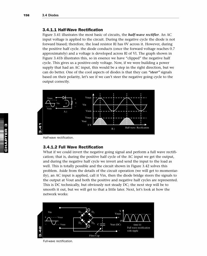
3.4.1.1 Half-Wave RectificationFigure 3.41 illustrates the most basic of circuits, the half-wave rectifier. An ACinput voltage is applied to the circuit. During the negative cycle the diode is notforward biased; therefore, the load resistor Rl has 0V across it. However, duringthe positive half cycle. the diode conducts (once the forward voltage reaches 0.7approximately) and a voltage is developed across Rl of Vl. The graph shown inFigure 3.41b illustrates this, so in essence we have “clipped” the negative halfcycle. This gives us a positive-only voltage. Now, if we were building a powersupply that had an AC input, this would be a step in the right direction, but wecan do better. One of the cool aspects of diodes is that they can “steer” signalsbased on their polarity, let’s see if we can’t steer the negative going cycle to theoutput correctly.
CH
AP
TE
R 3
VIVinVin
Vout
B.)
A.) VminVmin
Half wave Recification0 V
Vmax
VmaxVmax+ +
– –
Half-wave rectification.
3.4
1
3.4.1.2 Full Wave RectificationWhat if we could invert the negative going signal and perform a full wave rectifi-cation; that is, during the positive half cycle of the AC input we get the output,and during the negative half cycle we invert and send the input to the load aswell. This is totally possible and the circuit shown in Figure 3.42 solves thisproblem. Aside from the details of the circuit operation (we will get to momentar-ily), an AC input is applied, call it Vin, then the diode bridge steers the signals tothe output at Vout and both the positive and negative half cycles are represented.This is DC technically, but obviously not steady DC; the next step will be tosmooth it out, but we will get to that a little later. Next, let’s look at how thenetwork works:
Vin
Filter Cap
time (t) Full wave rectification with ripple
Vout (DC)
D3
D2
D1
D4 C0V
Vmin
VmaxV
Vmax+ +
–
–
1
2
Full-wave rectification.
3.4
2
04_0672328208_ch03.qxd 11/15/05 2:47 PM Page 156

1573.4 Diodes
Positive half cycle analysis—During the positive half cycle, the upper node 1 at thejunction of D3 and D1 is positive and the lower node 2 at the junction of D2 and D4 isnegative; therefore, the diodes D1 and D2 conduct, outputting the positive half cycle tothe + and – terminals.
Negative half cycle analysis—During the negative half cycle, the upper node 1 now hasa negative voltage on it while the lower node 2 has a positive voltage on it; this causesdiodes D4 and D3 to conduct and steer the signal out to the + and — terminals.
So, no matter what happens at the Vin input terminals the output voltage isalways positive going—very important.
CH
AP
TE
R 3
Please keep in mind that the diodes still need their forward conduction voltage of0.5–0.7V met before they will conduct, so the final output voltage will never be ashigh as the peak values of the input AC voltage; it will always be Vpeak – 0.7Vroughly.
Now that we have a fully rectified signal, can we use this for DC applications? Theanswer is no, the signal is not AC, but it’s varying DC, still no good to us. It hasto be stable at some voltage (preferably 5.0V for TTL logic), so we need to “regu-late” it more and filter it. One possibility that comes to mind is to place a filtercapacitor on the output Vout; let’s take a quick look at that since we are going tosee more of this design trick shortly.
The right half of Figure 3.42 shows the full wave rectifier circuit with an outputcapacitor on it, if we choose the output capacitor such that
Rload*C >> 1/fripple
Where Rload is across the output, then the discharge time of the RC network willbe much larger than the charging frequency, so the capacitor will never discharge.Where fripple is the ripple frequency calculated at 2 times the AC line frequency,for USA 60Hz AC this would be 120Hz. So, the question is what size capacitor arewe talking about here? Well, let’s say that we have a 100 ohm load resistance anda 120Hz fripple; we must choose C such that
C >> 1/(fripple*100 Ω)
Let’s assume “much greater” is 100x; then C would be
C = 100 / (120Hz*100 Ω) = 8333µF
This is typical for this kind of application. I would go ahead with a 10,000µF ormaybe even a 20,000µF to be safe. About as big as a D size battery. Next, let’s just
04_0672328208_ch03.qxd 11/15/05 2:47 PM Page 157

158 3.4 Diodes
see how much ripple voltage we would cause by draining the power with a load.We start with Iload = C*dv/dt:
Iload = C*dv/dt
rearranging a bit
dv = Iload *dt/C
and dt is just the small change in time per charging cycle; this is just the period(T) of the charging cycle, which is T = 1/f. Therefore we can write
dv = Iload / F*C
And at 120Hz with a filter capacitor of 20,000µF, and a load current of say 10mA,we are going to have a voltage ripple of
dv = 10mA / (120Hz * 20,000µF) = 4.1mV—not bad!
Although this seems reasonable, it’s still not stable enough for digital design’ weneed the voltage to stay very stable over large current drains. For example, adecent sized microcontroller can pull a couple hundred milliamperes; along withancillary hardware, the current drain of a basic embedded system (the XGS forexample) can be in the range of 500–1000mA. Let’s plug 500mA to see the results:
dv = 500mA / (120Hz * 20,000µF) = 208mV = .208 V
This is starting to get dangerous. The point being that we need something moreadvanced that can actively adjust the voltage and keep it steady under anycurrent drain; this is what a voltage regulator does, which we will get to in amoment. But, for now, realize this analysis and design is the first stage in yourpower system: rectification, filtering, and then finally regulation.
3.5 Voltage Regulation ApplicationsDiodes have so many wonderful properties that there are a lot of applications forthem that might now seem obvious. We have seen them used as rectifiers, butsince they have the property that their voltage stays nearly constant while theircurrent changes, we can take advantage of this to construct low voltage regula-tors. Take a look at Figure 3.43; here we see a circuit with 3 diodes in series, acurrent limiting resistor R, along with a load resistor RL, attached across the 3diodes in series. Now, let’s apply an input voltage Vin from 5V to 12V; no matterwhat voltage we apply to the input Vin, there is going to be conduction in thediode branch. The 100 ohm resistor R limits the maximum current to Vin/100,but other than that we will get conduction. Since the diodes are conducting
CH
AP
TE
R 3
04_0672328208_ch03.qxd 11/15/05 2:47 PM Page 158

1593.5 Voltage Regulation Applications
(hard) we will see a 0.7V drop across each for a total of 2.1V, so without a load wewill see 2.1V at Vout no matter what the input voltage. Now, if we apply a load,say 1000 ohm, what happens? The current It will split into two currents It = Id +IL, IL = 2.1V/1000Ω = 2.1mA, and as long as there is still enough voltage to keepthe diodes conducting, everything will be fine.
CH
AP
TE
R 3
R
RL
“Load Resistor”
Vin
2.1v
0.7
100 Ω
IL
It
Id
–
+
0.7–
+
0.7–
+
+
Diode based voltage regulator.
3.4
3
Again, this kind of regulation isn’t very stable and you have to series up a lot ofdiodes, and voltage drops over the diodes do change as you push more currentthrough them, but for simple applications it works great. For example, if you havea device that needs 4V rather than 5.0V then you simply put a couple diodes thathave a forward drop of 0.5V each in the current range you are going to draw andplace them in front of the device. Presto, you have a lower voltage supply that isreasonably stable, and as long as you don’t have a lot of current needs for thedevice then the voltage will stay reasonably stable. Figure 3.44 shows this design.
4 Volt device
+5V 0.5V 0.5V
4.0 V++
+
– –
Two-diode-based 4V voltage regulator.
3.4
4
04_0672328208_ch03.qxd 11/15/05 2:47 PM Page 159
160 3.5 Voltage Regulation Applications
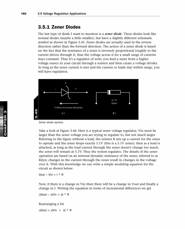
3.5.1 Zener Diodes The last type of diode I want to mention is a zener diode. These diodes look likenormal diodes (maybe a little smaller), but have a slightly different schematicsymbol as shown in Figure 3.45. Zener diodes are actually used in the reversedirection rather than the forward direction. The action of a zener diode is basedon the fact that the resistance of a zener is inversely proportional roughly to thecurrent driven through it, thus the voltage across it for a small range of currentsstays constant. Thus it’s a regulator of sorts; you feed a zener from a highervoltage source in your circuit through a resistor and then create a voltage divider.As long as the zener current is met and the current or loads stay within range, youwill have regulation.
CH
AP
TE
R 3
5.1 VZener
B.)A.)
V
I (flows in reverse direction)
+–
Zener diode symbol.
3.4
5
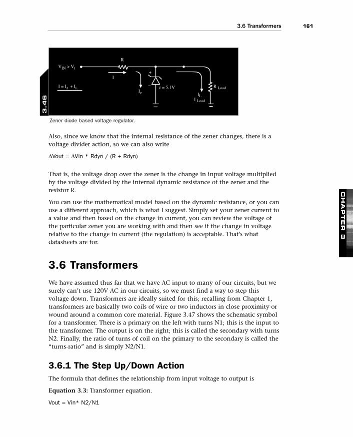
Take a look at Figure 3.46: Here is a typical zener voltage regulator; Vin must belarger than the zener voltage you are trying to regulate to, but not much larger.Referring to the figure without a load, the resistor R sets up a current for the zenerto operate and the zener drops exactly 5.1V (this is a 5.1V zener); then as a load isattached, as long as the load current through the zener doesn’t change too much,the zener will remain at 5.1V. Thus the system regulates. The details of the zeneroperation are based on an internal dynamic resistance of the zener, referred to asRdyn; changes in the current through the zener result in changes in the voltageover it. With this knowledge we can write a simple modeling equation for thecircuit as shown below:
Vout – Vin = I * R
Now, if there is a change in Vin then there will be a change in Vout and finally achange in I. Writing the equation in terms of incremental differences we get
∆Vout – ∆Vin = ∆I * R
Rearranging a bit
∆Vout = ∆Vin + ∆I * R
04_0672328208_ch03.qxd 11/15/05 2:47 PM Page 160
1613.6 Transformers
Also, since we know that the internal resistance of the zener changes, there is avoltage divider action, so we can also write
∆Vout = ∆Vin * Rdyn / (R + Rdyn)
That is, the voltage drop over the zener is the change in input voltage multipliedby the voltage divided by the internal dynamic resistance of the zener and theresistor R.
You can use the mathematical model based on the dynamic resistance, or you canuse a different approach, which is what I suggest. Simply set your zener current toa value and then based on the change in current, you can review the voltage ofthe particular zener you are working with and then see if the change in voltagerelative to the change in current (the regulation) is acceptable. That’s whatdatasheets are for.
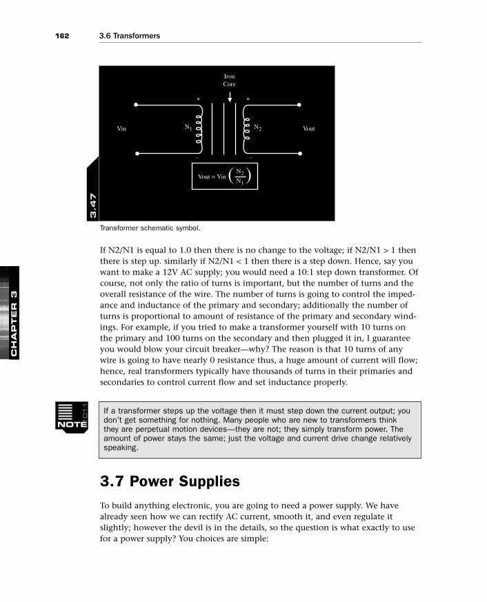
3.6 TransformersWe have assumed thus far that we have AC input to many of our circuits, but wesurely can’t use 120V AC in our circuits, so we must find a way to step thisvoltage down. Transformers are ideally suited for this; recalling from Chapter 1,transformers are basically two coils of wire or two inductors in close proximity orwound around a common core material. Figure 3.47 shows the schematic symbolfor a transformer. There is a primary on the left with turns N1; this is the input tothe transformer. The output is on the right; this is called the secondary with turnsN2. Finally, the ratio of turns of coil on the primary to the secondary is called the“turns-ratio” and is simply N2/N1.
3.6.1 The Step Up/Down ActionThe formula that defines the relationship from input voltage to output is
Equation 3.3: Transformer equation.
Vout = Vin* N2/N1
CH
AP
TE
R 3
VIN > Vt
I Load
R Load
R
+
–I = Iz + ILIz
I
IL
z = 5.1V
Zener diode based voltage regulator.
3.4
6
04_0672328208_ch03.qxd 11/15/05 2:47 PM Page 161
162 3.6 Transformers
If N2/N1 is equal to 1.0 then there is no change to the voltage; if N2/N1 > 1 thenthere is step up. similarly if N2/N1 < 1 then there is a step down. Hence, say youwant to make a 12V AC supply; you would need a 10:1 step down transformer. Ofcourse, not only the ratio of turns is important, but the number of turns and theoverall resistance of the wire. The number of turns is going to control the imped-ance and inductance of the primary and secondary; additionally the number ofturns is proportional to amount of resistance of the primary and secondary wind-ings. For example, if you tried to make a transformer yourself with 10 turns onthe primary and 100 turns on the secondary and then plugged it in, I guaranteeyou would blow your circuit breaker—why? The reason is that 10 turns of anywire is going to have nearly 0 resistance thus, a huge amount of current will flow;hence, real transformers typically have thousands of turns in their primaries andsecondaries to control current flow and set inductance properly.
CH
AP
TE
R 3
VoutN1 N2Vin
IronCore
+ +
–
N2
N1Vout = Vin ( )
–
Transformer schematic symbol.
3.4
7
3.7 Power SuppliesTo build anything electronic, you are going to need a power supply. We havealready seen how we can rectify AC current, smooth it, and even regulate itslightly; however the devil is in the details, so the question is what exactly to usefor a power supply? You choices are simple:
If a transformer steps up the voltage then it must step down the current output; youdon’t get something for nothing. Many people who are new to transformers think they are perpetual motion devices—they are not; they simply transform power. Theamount of power stays the same; just the voltage and current drive change relativelyspeaking.
04_0672328208_ch03.qxd 11/15/05 2:47 PM Page 162
1633.7 Power Supplies
1. Battery power.
2. Buy a power supply.
3. Use a wall transformer and a voltage regulator circuit to derive the voltageyou need.
All choices are appropriate in the right circumstances. For example, once yourdesign is complete and you want to make it mobile, you might want to makeyour project battery powered. This design is nothing more than solution 3 withDC battery power rather than AC converted to DC with a wall transformer orbridge rectifier: You will still have to regulate the battery power since the voltageon the batteries will change as you load them. Solution 2 is what you will needfor most of your designs; that is, you may need many different voltages in yoursystem designs and you may need to adjust voltages and experiment. The onlyway to do this is to build an adjustable voltage supply (not a good idea yet) or tojust buy one for $50–200. The last choice if you know what voltage you need is tosimply build a power supply into your system or on another board that you canuse; let’s focus on that one (which is also applicable to 1).
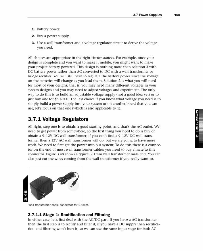
3.7.1 Voltage RegulatorsAll right, step one is to obtain a good starting point, and that’s the AC outlet. Weneed to get power from somewhere, so the first thing you need to do is buy orobtain a 9–12V DC wall transformer; if you can’t find a 9–12V DC wall trans-former then a 12V AC wall transformer will do, but we are going to have morework. We need to first get the power into our system: To do this there is a connec-tor on the end of most wall transformer cables; you need to buy a mate to thisconnector. Figure 3.48 shows a typical 2.1mm wall transformer male end. You canalso just cut the wires coming from the wall transformer if you really want to.
CH
AP
TE
R 3
Wall transformer cable connector for 2.1mm.
3.4
8
3.7.1.1 Stage 1: Rectification and FilteringIn either case, let’s first deal with the AC/DC part. If you have a AC transformerthen the first step is to rectify and filter it; if you have a DC supply then rectifica-tion and filtering won’t hurt it, so we can use the same input stage for both AC
04_0672328208_ch03.qxd 11/15/05 2:47 PM Page 163
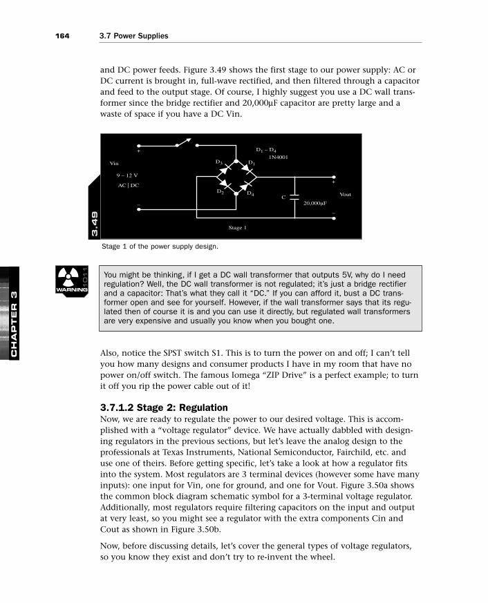
164 3.7 Power Supplies
and DC power feeds. Figure 3.49 shows the first stage to our power supply: AC orDC current is brought in, full-wave rectified, and then filtered through a capacitorand feed to the output stage. Of course, I highly suggest you use a DC wall trans-former since the bridge rectifier and 20,000µF capacitor are pretty large and awaste of space if you have a DC Vin.
CH
AP
TE
R 3
Vin
Vout
9 – 12 V
C
D1 – D4
20,000µF
AC | DC
Stage 1
1N4001D1
D2
D3
D4
+
+
–
_
Stage 1 of the power supply design.
3.4
9
Also, notice the SPST switch S1. This is to turn the power on and off; I can’t tellyou how many designs and consumer products I have in my room that have nopower on/off switch. The famous Iomega “ZIP Drive” is a perfect example; to turnit off you rip the power cable out of it!
3.7.1.2 Stage 2: RegulationNow, we are ready to regulate the power to our desired voltage. This is accom-plished with a “voltage regulator” device. We have actually dabbled with design-ing regulators in the previous sections, but let’s leave the analog design to theprofessionals at Texas Instruments, National Semiconductor, Fairchild, etc. anduse one of theirs. Before getting specific, let’s take a look at how a regulator fitsinto the system. Most regulators are 3 terminal devices (however some have manyinputs): one input for Vin, one for ground, and one for Vout. Figure 3.50a showsthe common block diagram schematic symbol for a 3-terminal voltage regulator.Additionally, most regulators require filtering capacitors on the input and outputat very least, so you might see a regulator with the extra components Cin andCout as shown in Figure 3.50b.
Now, before discussing details, let’s cover the general types of voltage regulators,so you know they exist and don’t try to re-invent the wheel.
You might be thinking, if I get a DC wall transformer that outputs 5V, why do I needregulation? Well, the DC wall transformer is not regulated; it’s just a bridge rectifierand a capacitor: That’s what they call it “DC.” If you can afford it, bust a DC trans-former open and see for yourself. However, if the wall transformer says that its regu-lated then of course it is and you can use it directly, but regulated wall transformersare very expensive and usually you know when you bought one.
04_0672328208_ch03.qxd 11/15/05 2:47 PM Page 164

1653.7 Power Supplies
Linear Regulators—These are the standard 3-terminal regulators that are used mostcommonly; they regulate a higher voltage down to a smaller voltage. Typically, theycome in voltages 5–24V: Some are fixed, some are variable. The input voltage usuallyhas to be 2–3V greater than the target voltage to regulate to. These regulators come ina number of packages including the TO220/202, TO92, and TO3, as shown in Figure3.51. Linear regulators are usually DC-DC, meaning DC in DC out.
CH
AP
TE
R 3
Vin
Vin Vout
Vout
Cin
Regulated DCUnregulated DCRegulator
Regulator
Cout
A.)
B.)
Vin VoutGnd
Vin VoutGnd
+
+ +
+
–
–
–
–
Block diagram of 3-terminal voltage regulator.
3.5
0
Regulator packages.
3.5
1
Switching Regulators—Switching regulators are more exotic and can either step downa voltage or step it up (and even invert it). These regulators usually come in surfacemount packages and are highly efficient. Additionally, they may have many more pinsthan linear regulators and may need external capacitors and inductors. Internally, they
04_0672328208_ch03.qxd 11/15/05 2:47 PM Page 165

166 3.7 Power Supplies
operate by generating an AC signal from the input DC signal and then using it to gener-ate any voltage needed via capacitive and inductive networks. Again, switching regula-tors are DC-DC.
Charge Pumps—Charge pumps are usually used to generate high voltages from smallvoltages and are usually DC-DC converters. However, they have very little current driveand thus are used in applications where very large voltages are needed, but very littlecurrent, such as LCD applications. In general, we will use linear and switching regula-tors in all our work, with the emphasis on linear regulators since they are so easy tohook up.
3.8 Example Power Supply DesignsLet’s get right into some design with example voltage supplies that are commonlyneeded in embedded systems: 5.0V, 3.3V, and 12V (for robotics enthusiasts).
3.8.1 5V with the LM/UA7805The “7805” is probably one of the most well-known voltage regulators on theplanet. The most common supply voltage for hobbyist and simple embeddedsystems is 5.0V (although this is changing rapidly to 3.3V); moreover, the 5.0Vsupply is the single supply needed in most systems, so anyone who has even builta single board computer or an embedded system has probably used a 7805 orderivative. As noted there are a number of manufacturers that make 7805 regula-tors; take your pick, for now we will just assume we are going to use the TexasInstruments variation named the UA7805. Figure 3.52 shows an excerpt from thedatasheet. The 7805 usually comes in a TO220 package, although it can be foundfrom other manufacturers in a TO92 package like a transistor comes in. In anycase, the 7805 is so ubiquitous you don’t even have to look at the datasheet tohook one up, but we might as well just for the exercise, so please go to the TexasInstruments website at http://www.ti.com and search for “UA7805”, and down-load and view the datasheet. Or you can find it on the CD in
CDROOT:\DATASHEETS\ua7805.pdf
Open the datasheet up either way and take a look at it; there is a lot of informa-tion. The beginning of a datasheet usually shows the product pictures and someof the package options, then come the DC/AC characteristics, next the applicationnotes, and finally the mechanical data. Of course this isn’t set in stone and youwill see variations, but in most cases, you will find all of these sections in anyreputable company’s datasheet. Once you’re done looking, find the exampleapplications and take a look at the “fixed-regulator” example. As you can see, theapplication notes show the regulator connected with a Cin of 0.33µF and a Cout
CH
AP
TE
R 3
04_0672328208_ch03.qxd 11/15/05 2:47 PM Page 166
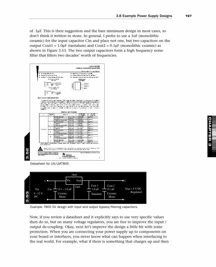
1673.8 Example Power Supply Designs
of .1µF. This is their suggestion and the bare minimum design in most cases, sodon’t think it written in stone. In general, I prefer to use a 1uF (monolithicceramic) for the input capacitor Cin and place not one, but two capacitors on theoutput Cout1 = 1.0µF (tantalum) and Cout2 = 0.1µF (monolithic ceramic) asshown in Figure 3.53. The two output capacitors form a high frequency noisefilter that filters two decades’ worth of frequencies.
CH
AP
TE
R 3
Datasheet for UA/LM7805.
3.5
2
Now, if you review a datasheet and it explicitly says to use very specific valuesthen do so, but on many voltage regulators, you are free to improve the input /output de-coupling. Okay, next let’s improve the design a little bit with someprotection. When you are connecting your power supply up to components onyour board or interfaces, you never know what can happen when interfacing tothe real world. For example, what if there is something that charges up and then
Vin
9 - 12 V
7805
Vin Vout
Vout = 5 V DCRegulated
CinGnd
DCCeramicMono
Tantalum CeramicMono
Cout 11.0 µF0.1 – 1.0 µF 0.1 µF
Cout 2
– –
+ +
Example 7805 5V design with input and output bypass/filtering capacitors.
3.5
3
04_0672328208_ch03.qxd 11/15/05 2:47 PM Page 167
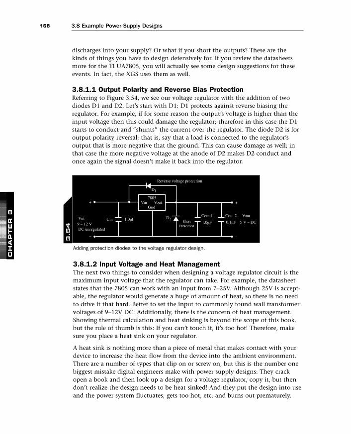
168 3.8 Example Power Supply Designs
discharges into your supply? Or what if you short the outputs? These are thekinds of things you have to design defensively for. If you review the datasheetsmore for the TI UA7805, you will actually see some design suggestions for theseevents. In fact, the XGS uses them as well.
3.8.1.1 Output Polarity and Reverse Bias ProtectionReferring to Figure 3.54, we see our voltage regulator with the addition of twodiodes D1 and D2. Let’s start with D1: D1 protects against reverse biasing theregulator. For example, if for some reason the output’s voltage is higher than theinput voltage then this could damage the regulator; therefore in this case the D1starts to conduct and “shunts” the current over the regulator. The diode D2 is foroutput polarity reversal; that is, say that a load is connected to the regulator’soutput that is more negative that the ground. This can cause damage as well; inthat case the more negative voltage at the anode of D2 makes D2 conduct andonce again the signal doesn’t make it back into the regulator.
CH
AP
TE
R 3 Vin
9 – 12 V
Vout
Reverse voltage protection
DC unregulated
ShortProtection
Cin D2
D1
7805Vin Vout
Gnd
Cout 11.0µF
5 V – DC0.1µF1.0µF
Cout 2
+ +
– –
Adding protection diodes to the voltage regulator design.
3.5
4
3.8.1.2 Input Voltage and Heat ManagementThe next two things to consider when designing a voltage regulator circuit is themaximum input voltage that the regulator can take. For example, the datasheetstates that the 7805 can work with an input from 7–25V. Although 25V is accept-able, the regulator would generate a huge of amount of heat, so there is no needto drive it that hard. Better to set the input to commonly found wall transformervoltages of 9–12V DC. Additionally, there is the concern of heat management.Showing thermal calculation and heat sinking is beyond the scope of this book,but the rule of thumb is this: If you can’t touch it, it’s too hot! Therefore, makesure you place a heat sink on your regulator.
A heat sink is nothing more than a piece of metal that makes contact with yourdevice to increase the heat flow from the device into the ambient environment.There are a number of types that clip on or screw on, but this is the number onebiggest mistake digital engineers make with power supply designs: They crackopen a book and then look up a design for a voltage regulator, copy it, but thendon’t realize the design needs to be heat sinked! And they put the design into useand the power system fluctuates, gets too hot, etc. and burns out prematurely.
04_0672328208_ch03.qxd 11/15/05 2:47 PM Page 168
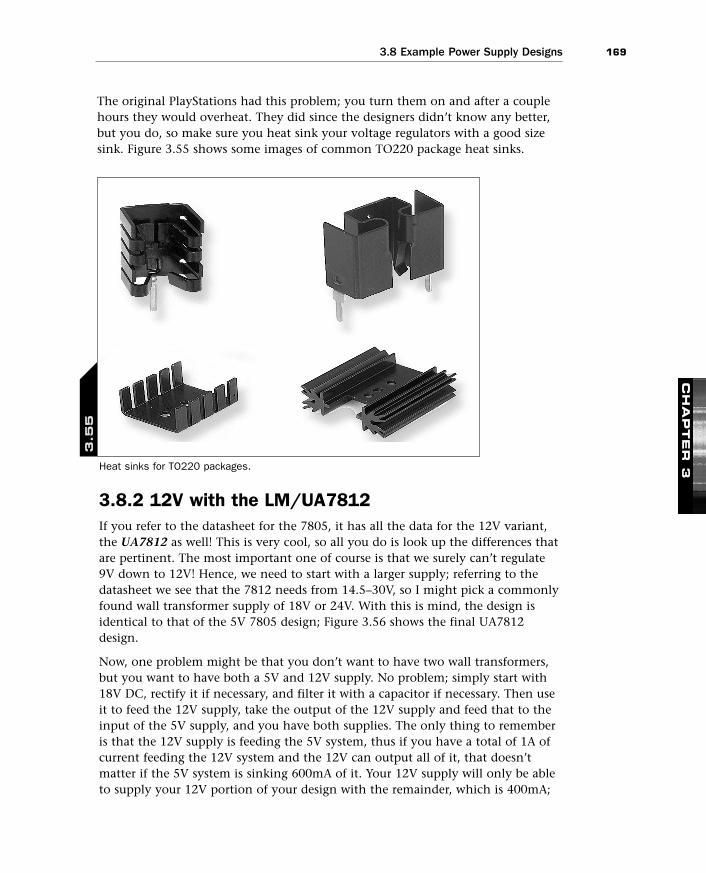
1693.8 Example Power Supply Designs
The original PlayStations had this problem; you turn them on and after a couplehours they would overheat. They did since the designers didn’t know any better,but you do, so make sure you heat sink your voltage regulators with a good sizesink. Figure 3.55 shows some images of common TO220 package heat sinks.
CH
AP
TE
R 3Heat sinks for TO220 packages.
3.5
5
3.8.2 12V with the LM/UA7812If you refer to the datasheet for the 7805, it has all the data for the 12V variant,the UA7812 as well! This is very cool, so all you do is look up the differences thatare pertinent. The most important one of course is that we surely can’t regulate9V down to 12V! Hence, we need to start with a larger supply; referring to thedatasheet we see that the 7812 needs from 14.5–30V, so I might pick a commonlyfound wall transformer supply of 18V or 24V. With this is mind, the design isidentical to that of the 5V 7805 design; Figure 3.56 shows the final UA7812design.
Now, one problem might be that you don’t want to have two wall transformers,but you want to have both a 5V and 12V supply. No problem; simply start with18V DC, rectify it if necessary, and filter it with a capacitor if necessary. Then useit to feed the 12V supply, take the output of the 12V supply and feed that to theinput of the 5V supply, and you have both supplies. The only thing to rememberis that the 12V supply is feeding the 5V system, thus if you have a total of 1A ofcurrent feeding the 12V system and the 12V can output all of it, that doesn’tmatter if the 5V system is sinking 600mA of it. Your 12V supply will only be ableto supply your 12V portion of your design with the remainder, which is 400mA;
04_0672328208_ch03.qxd 11/15/05 2:47 PM Page 169

170 3.8 Example Power Supply Designs
thus consider that if you do feed your 5V from a 12V then part of the 12V currentdrive is going to disappear to power the 5V.
CH
AP
TE
R 3
18 – 24 VDC – unregulated
D2
D1
Vin7812
VoutGnd
Cout 11µF 1.0µF
12 VDC0.1µF
Cout 2
+ +
– –
12V voltage regulator design.
3.5
6
3.8.3 3.3V with the TI TPS76933DBVT3.3V is becoming the new standard for embedded systems. Ironically, it’s alreadytwo generations old; there are already 1.8V and 1.5V systems, and 1.2V are start-ing to show up as well. However, most manufacturers are about 3–5 years awayfrom completely phasing out 5.0V, so 3.3V is still on its climb, so we don’t haveto worry too much about 1.8V and 1.5V yet as hobbyists. In any case, there are alot of choices for 3.3V regulators from a lot of manufacturers, but I have used alot of them and found the Texas Instruments TPS76933DBVT to be easy to use,cheap, and work well. You can find it online at http://www.ti.com as usual, orlook at the datasheet located on the CD in
CDROOT:\DATASHEETS\tps76933.pdf.
Figure 3.57 shows the device’s first datasheet page. Referring to the datasheet, thefirst thing you are going to notice is that this is what’s called a surface mountdevice (SMT or surface mount technology). That is, you can’t place it in a bread-board or experimenter board; you have to either solder directly to it or get specialSMT-to-through-hole DIP (dual in-line package) converters. Not to worry though,the company below
http://www.beldynsys.com
has a whole line of surface-mount-to-DIP and -through-hole converters. Basically,they make circuit boards that you solder your SMT parts onto and then you usethe circuit boards (very small) as if they were through hole parts! Figure 3.58shows some of their products.
04_0672328208_ch03.qxd 11/15/05 2:47 PM Page 170
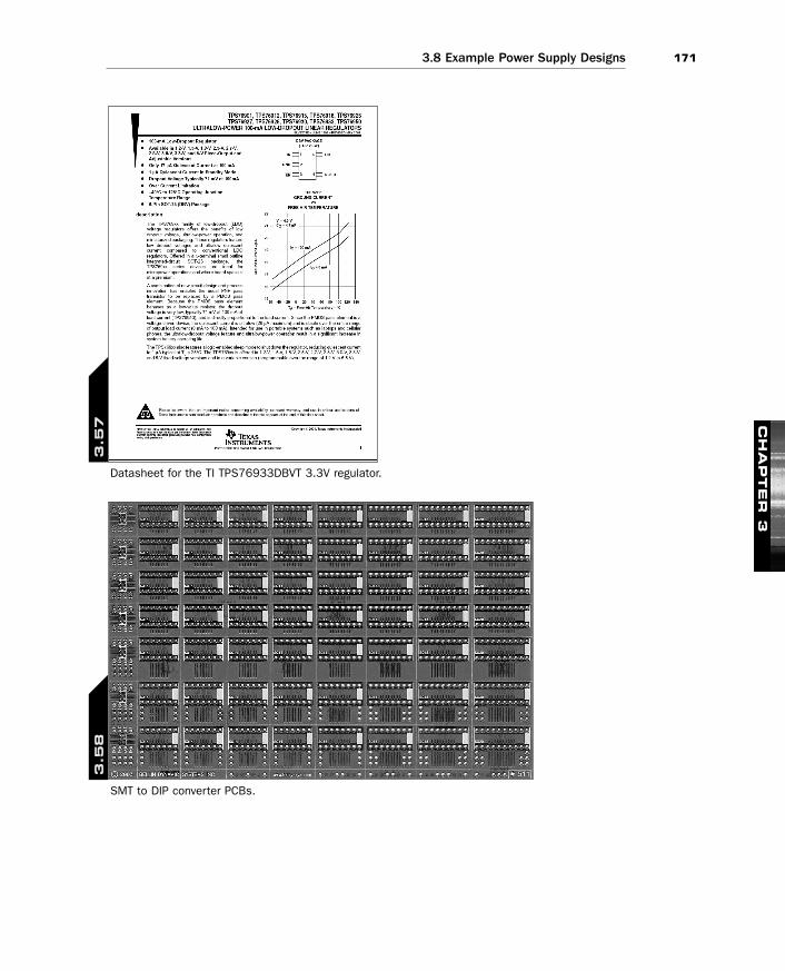
1713.8 Example Power Supply Designs
CH
AP
TE
R 3
Datasheet for the TI TPS76933DBVT 3.3V regulator.
3.5
7
SMT to DIP converter PCBs.
3.5
8
04_0672328208_ch03.qxd 11/15/05 2:47 PM Page 171

172 3.8 Example Power Supply Designs
Aside from the fact that the regulator is SMT, it’s a great little device. It has 5 pins,and comes in a SOT-23, which means there are a total of 5 pins/contacts: 3 onone side, 2 on the other; refer to the datasheet. The pins are defined as follows:
IN—Input voltage 2–10V.
OUT—Regulated 3.3V.
/EN—Regulator enable (active LOW); tie this to ground for the regulator to operate.
GND—System ground.
NC—No connection.
The only thing different about this regulator is that it has an enable pin, which isgood if you want to digitally control a power supply, and that it’s surface mount.Now, let’s design a power supply with it. Once again, we assume that the stage 1of the power supply is already in place and we are being fed power from that, butit’s not regulated. However, we have a decision to make: We can either feed fromthe main lines, which could be at 9–12V DC (however, the 12V would exceed thedatasheet spec), but that’s not an option. Thus, we have to consider feeding froma lower supply like the 5V regulated supply. Of course, if we were making just a3.3V system then we would design it such that the input from the wall trans-former was 6–9V DC rather than 9–12V DC, but let’s assume that we have alreadycreated a regulated 5V supply in the system and that’s what we are going to feedthe 3.3V regulator.
3.8.3.1 Following the DatasheetThe datasheet for the TPS76933DBVT is much more strict than the 7805, espe-cially when it comes to the bypass/stability capacitors. Now, since I always overdothings I am fine, but many engineers under-design, and this is a part that can getthose kind of guys in trouble. For example, if you refer to the datasheet for theTPS76933DBVT on page 11, the suggested design for the regulator C1 is 1.0µF,which is fine, but the capacitor across Vout is rated to be a minimum of 4.7µF andit has an ESR spec (equivalent series resistance—remember that?). So not only doyou have to use a larger capacitor, you have to make sure that the internal resis-tance of the capacitor meets the ESR spec. Now, don’t get too worried; I will tellyou right now, first use a larger capacitor (the spec says bigger is better), so 10µFwill do, Make sure it’s tantalum and I guarantee you will be fine; you can look atthe ESR (if you can find it) for the cap you have, but chances are you simply havesome in your parts box and have no idea who made them, so we hedge our betsby using the larger suggestion and also reading that the larger cap allows smallerESR values. With all that in mind, Figure 3.59 shows our design for the 3.3V regu-lator. Notice that I still added the protection diodes and I added another capacitorCout2 = 0.1µF (ceramic monolithic) for high frequency noise.
CH
AP
TE
R 3
04_0672328208_ch03.qxd 11/15/05 2:47 PM Page 172
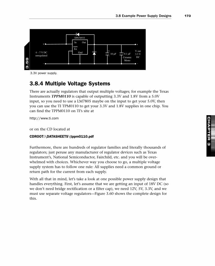
1733.8 Example Power Supply Designs
3.8.4 Multiple Voltage SystemsThere are actually regulators that output multiple voltages; for example the TexasInstruments TPPM0110 is capable of outputting 3.3V and 1.8V from a 5.0Vinput, so you need to use a LM7805 maybe on the input to get your 5.0V, thenyou can use the TI TPM0110 to get your 3.3V and 1.8V supplies in one chip. Youcan find the TPPM0110 on TI’s site at
http://www.ti.com
or on the CD located at
CDROOT:\DATASHEETS\tppm0110.pdf
Furthermore, there are hundreds of regulator families and literally thousands ofregulators; just peruse any manufacturer of regulator devices such as TexasInstrument’s, National Semiconductor, Fairchild, etc. and you will be over-whelmed with choices. Whichever way you choose to go, a multiple voltagesupply system has to follow one rule: All supplies need a common ground orreturn path for the current from each supply.
With all that in mind, let’s take a look at one possible power supply design thathandles everything. First, let’s assume that we are getting an input of 18V DC (sowe don’t need bridge rectification or a filter cap), we need 12V, 5V, 3.3V, and wemust use separate voltage regulators—Figure 3.60 shows the complete design forthis.
CH
AP
TE
R 3
In
4 – 7 V DCunregulated
CeramicMono
Out
TPS76933
Gnd
En
10 µFV out3.3 VDC
0.1 µF
+ +
+
– –
–
3.3V power supply.
3.5
9
04_0672328208_ch03.qxd 11/15/05 2:47 PM Page 173
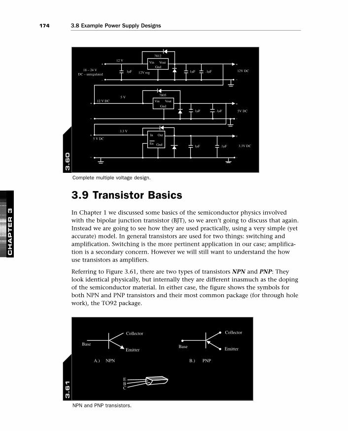
174 3.8 Example Power Supply Designs
3.9 Transistor BasicsIn Chapter 1 we discussed some basics of the semiconductor physics involvedwith the bipolar junction transistor (BJT), so we aren’t going to discuss that again.Instead we are going to see how they are used practically, using a very simple (yetaccurate) model. In general transistors are used for two things: switching andamplification. Switching is the more pertinent application in our case; amplifica-tion is a secondary concern. However we will still want to understand the howuse transistors as amplifiers.
Referring to Figure 3.61, there are two types of transistors NPN and PNP: Theylook identical physically, but internally they are different inasmuch as the dopingof the semiconductor material. In either case, the figure shows the symbols forboth NPN and PNP transistors and their most common package (for through holework), the TO92 package.
CH
AP
TE
R 3
18 – 24 V DC – unregulated
Vin
7812
VoutGnd
1µF 1µF
12 V
5 V
5 V DC
12V DC
12 V DC
12V reg .1µF
+
+
+
–
–
– –
–
Vin
7805
Vout
Gnd1µF
1µF
3.3 V
3.3V DC
5V DC.1µF
.1µF
+
+ +
–
In Out
GndEn
Complete multiple voltage design.
3.6
0
A.) B.) PNPNPN
BC
E
Collector
Base EmitterEmitter
Collector
Base
NPN and PNP transistors.
3.6
1
04_0672328208_ch03.qxd 11/15/05 2:47 PM Page 174

1753.9 Transistor Basics
The only difference between NPN and PNP as far as their schematic symbols go isthe direction of the arrow on the emitter lead. For NPN the emitter arrow pointsaway from the base or body of the transistor; for PNP the emitter arrow pointstoward the base or body of the transistor.
That’s all fine and dandy, but what does a transistor do? It basically allows you tocontrol a secondary circuit with a small current or voltage in another primarycircuit. For example, we can switch on a large amount of current with a smallcurrent, or we can use transistor to create digital gates, etc. The point is that theability to turn on/off another circuit, thereby mimicking a mechanical relay, isvery powerful, so transistors in one configuration are devices that allow us tocontrol current in another circuit in a digital on/off manner. Additionally, transis-tors can be used as amplifiers. With that in mind, we can model a transistor as acurrent controlled switch or resistor with the following properties.
3.9.1 Transistor Properties and RulesThe rules we are going to derive are for the NPN transistor; for the PNP all polari-ties are simply inverted, but the operation is the same other than that. Please referto Figure 3.62 for this discussion. Here are the rules:
CH
AP
TE
R 3
E
C
BIC
IB
(A.) NPN (B.) PNP
E
C
BIC
IB
Transistor analysis model.
3.6
2
Rule 1: The collector voltage must always be greater than the emitter by approximately0.2V.
Rule 2: The base-emitter and base-collector circuits in a transistor act like diodes. Thebase-emitter diode is forward biased and conducting when the transistor is operating.The base-collector diode is reverse-biased and not conducting. This should seem like aparadox, and it is. Since internally transistors are not just diodes, we are doing a littlehand waving here, so don’t feel uneasy if you look at the figure and see current flowingthrough a reverse biased diode: Remember there is no diode there. Using a couplediodes to help you understand parts of the transistor operation is okay—but in realitytransistors do not act like diodes!
Rule 3: Transistors all have maximum current and voltage ratings. Some of the valuesof importance are IB (base current), IC (collector current), IE (emitter current), not
04_0672328208_ch03.qxd 11/15/05 2:47 PM Page 175
176 3.9 Transistor Basics
shown here yet. Also there are the voltages VBE (base-emitter), VCE (collector-emitter),and so forth.
Rule 4: Now comes the fun part: So as long as the collector voltage is greater than theemitter voltage and we don’t exceed any of the voltage maximums, the transistor“action” will occur. This action describes the relationship between the currents in thetransistor. This relationship is
Equation 3.4: Transistor base/collector current relationship.
IC = hFE*IB = β*IB
hFE and or β (beta) is called the current gain, beta, or just plain gain of the tran-sistor, and is a measure of the current amplification from the base current to thecollector current. For common transistors such as the 2N3904/3906, the gain isanywhere from 50–250. A reasonable average gain to count on is 100 minimum.
CH
AP
TE
R 3
Once again, please don’t think you are getting something for nothing; the transistor issimply a current controlled resistor for all intents and purposes. You send a currentin, you get a larger current out; however, this output current is coming from the powersupply, so you don’t get something for nothing. Also, many new designers use thegain in their designs—do NOT do this. Gain is only an estimate and varies. You neverwant to assume that the gain is some value and then use it in your calculations. Ifyou design your circuit properly the gain of the transistor is irrelevant to your circuitgain..
So the gain formula tells us that a small amount of base current causes a largeamount of collector current. This is the key to the transistor, its current amplifica-tion ability. Also, since the base-emitter leg of the transistor is very similar to adiode, we can even model the diode drop properly; in other words when youapply a voltage to the base, the base-emitter diode will drop about 0.6–0.7V, nomatter what. Or in other words, you cannot ever apply a voltage across the base-emitter junction greater than this or you will destroy the transistor. Therefore, wecan write this modeling equation:
VB = VE + VBE (approximately 0.6–0.7V)
Most people just use 0.6V and be done with it, resulting in
Equation 3.5: Transistor base-emitter voltage relationship.
VB = VE + 0.6V
And of course, all this is reversed for PNP, but luckily for us in digital electronics+5V= “1”, +0V = “0”, and a positive voltage happens to turn on a NPN transistor,so you will tend to use NPN transistors only in your designs! Lastly, try not to
04_0672328208_ch03.qxd 11/15/05 2:47 PM Page 176
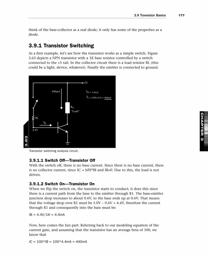
1773.9 Transistor Basics
think of the base-collector as a real diode; it only has some of the properties as adiode.
3.9.1 Transistor SwitchingAs a first example, let’s see how the transistor works as a simple switch. Figure3.63 depicts a NPN transistor with a 1K base resistor controlled by a switchconnected to the +5 rail. In the collector circuit there is a load resistor RL (thiscould be a light, device, whatever). Finally the emitter is connected to ground.
CH
AP
TE
R 3
IB
RC
IO = 4.4mA
“Load”
IL = (100) (4.4) = 440mA
440mA
4.4V
1K
+5V
Transistor switching analysis circuit.
3.6
3
3.9.1.1 Switch Off—Transistor OffWith the switch off, there is no base current. Since there is no base current, thereis no collector current, since IC = hFE*IB and IB=0. Due to this, the load is notdriven.
3.9.1.2 Switch On—Transistor OnWhen we flip the switch on, the transistor starts to conduct; it does this sincethere is a current path from the base to the emitter through R1. The base-emitterjunction drop increases to about 0.6V, so the base ends up at 0.6V. That meansthat the voltage drop over R1 must be 5.0V – 0.6V = 4.4V, therefore the currentthrough R1 and consequently into the base must be:
IB = 4.4V/1K = 4.4mA
Now, here comes the fun part: Referring back to our modeling equation of thecurrent gain, and assuming that the transistor has an average beta of 100, weknow that
IC = 100*IB = 100*4.4mA = 440mA
04_0672328208_ch03.qxd 11/15/05 2:47 PM Page 177
178 3.9 Transistor Basics
Is this right? Yes, but it’s not good; remember the beta may vary wildly from onetransistor to another, but if you design assuming that beta can range from 50–250then you would be covered. And in a switch like this, that would be easy. In anycase, continuing the analysis, we see that the collector current is 440mA—that’s alot of current, but is this possible? This depends on the load. If the load was 10ohms then the voltage across the load would be
Vload = 440mA * 10Ω = 4.4V
Therefore, the voltage at the collector itself VC is still above the emitter by at least.2V, so we are okay. But let’s up the load to 100 ohms and see what happens. At100 ohms, the voltage drop would be
Vload = 440mA * 100Ω = 44V
Which is actually funny and makes no sense since the supply is only 5V.However, you would be amazed at how many people would leave this as ananswer on a test. Anyway, something’s got to give. And that something is thecurrent, so we assume that the transistor will only allow enough current such thatthe voltage VC is 0.2V greater than the emitter voltage VE (which is at ground).Or in other words, VC = 0.2V; therefore, the voltage drop over our 100 ohm loadwill be
Vload = 5V – 0.2V = 4.8V
and the current through the 100 ohm load is
Iload = IC = 4.8V / 100Ω = 48mA
Therefore, the circuit can only supply 48mA to a load of 100 ohms, but cansupply 440mA to a load of 10 ohms.
This is basically how transistors are used as switches. You control the base with avoltage or current to turn the “switch” on or off, and then based on the collectorcircuit design, it serves whatever purpose you need.
3.9.2 Emitter Followers and Impedance ReflectionAnother interesting use for transistors is what’s called “emitter followers”; that is,using a transistor to “pass” a voltage to another stage untouched, with the addedbenefit that the transistor’s base has huge impedance, which is good for the inputsignal. Let’s take a look at this property by referring to Figure 3.64. We know thatthe base voltage VB is always 0.6V or so higher than the emitter voltage VE, solet’s just turn this equation around like this:
VE = VB – 0.6V
CH
AP
TE
R 3
04_0672328208_ch03.qxd 11/15/05 2:47 PM Page 178

1793.9 Transistor Basics
And presto, you have a voltage follower. That is, whatever voltage you apply tothe base, the emitter follows it with a slight translation (decrease) of 0.6V.However, there are limits to this of course. You must make sure that VBE is always0.6V; if it’s less, the transistor will stop conduction, and of course you must havethe emitter resistor there to create a voltage drop. The reason why is if you put 3Von the base, and the emitter was tied directly to ground, then you would damagethe transistor, since we must maintain the property that the base-emitter junctionnever has more than approximately 0.6V across it.
All right, the voltage following capability is interesting, but is there anything elsewe can get from this configuration? The answer is impedance reflection, or inother words, when you are sending a signal from one part of the circuit toanother, you don’t want to load your output: You want the input to the nextstage to have infinite impedance if possible (unless you are transferring power,then you want to match the impedance). This is hard to do when the load canchange, but with a transistor you can “reflect” the load through the transistor’sgain and multiply the apparent impedance by the gain factor. The analysisfollows.
First, we need to slightly modify our current model and define IE:
IE = IB + IC
In most cases, IE = IC since IB is so small, but in this case, let’s use a more exactmodel. Plugging in the fact that IC = hFE*IB, we get:
IE = IB + hFE*IB = IB*(1 + hFE)
CH
AP
TE
R 3
IB
RC
IO = 4.4mA
“Load”
IL = (100) (4.4) = 440mA
440mA
4.4V
1K
+5V
Circuit to demonstrate impedance reflection.
3.6
4
04_0672328208_ch03.qxd 11/15/05 2:47 PM Page 179

180 3.9 Transistor Basics
Therefore,
IB = IE / (1 + hFE)
And we know that VE = VB – 0.6, but if are looking at the differences in VB andVE then we can write
∆VE = ∆VB
Computing the current thru R, we get
∆IE = (∆VE / R) = (∆VB / R)
And combining the results, we get:
∆IB = ∆VB / [R*(1 + hFE)]
Paying close attention to this result, we see that the load impedance R seen fromthe base is not just R, but R multiplied by (1+hFE). Or in other words, if there wasa 1K load R and the gain of the transistor was 100 nominal then using an emitterfollower “reflects” the impedance and multiplies it by the gain, resulting in100*1K = 100K of equivalent input impedance. That is very useful; we justunloaded the output by a factor of 100 in comparison to if we were just drivingthe 1K directly.
3.9.3 AmplificationThe transistor modeling for amplification is a little more complex than for aswitch, so we don’t need to cover it. However, I do want to leave you with ageneral circuit for amplification of small signals with AC coupling and somediscussion of its operation. Figure 3.65 is a nice single stage transistor amplifierwith high pass filters on the input and output and “voltage divider” biasing.
Remember, the transistor always has the ability to amplify current, but if youwant to amplify a voltage such as an audio signal then you must first realize thatthe audio signal is very small, and it’s probably AC. So step one is to “AC couple”the signal into the amplifier, so you don’t amplify the DC component; this isaccomplished at C1. Only AC will pass through C1, so the small signal will getthrough, but whatever DC component will get blocked. Next we see that the baseof the transistor is biased such that the resistors R1 and R2 create a voltage dividernetwork; we would want to set the voltage of the base, which is somewhere in themiddle of the voltage supply, so that we can swing the input as large as possibleand with symmetry. The actual voltage on VB will of course be
VB = VCC * R2/ (R1+R2)
CH
AP
TE
R 3
04_0672328208_ch03.qxd 11/15/05 2:48 PM Page 180

1813.9 Transistor Basics
Additionally, we should note that the C1 and the parallel combination of R1||R2create a high pass filter.
Okay, next we need an output load resistor to drop the output signal on; this isRL. Attached to RL’s top node is another capacitor C2, which once again ACcouples the signal out of the amplifier without any DC component. And of courseC2 and RL create yet another high pass filter.
Now, to actually select the values of the resistors and capacitors we have to decideon a few things, but the interesting part will be that the final gain of the circuitwill have nothing to do with the gain hFE! And that’s what we want—gain invari-ance: We want the gain to be a function of the component values which we cancontrol, not a random process on the transistor. In any event, let’s set somevalues. If VCC is 5V and we want to maximize output swing then we assume thatVE is at 2.5V; given that we know that RL has a 2.5V drop over it, but we need todecide on the quiescent operating point. That is, how much current flows with noinput. A good range might be from 100µA to 10mA, so let’s pick something in themiddle with easy math: 1.0mA. Therefore, if there is 1.0mA flowing through RLwith a voltage drop of 2.5V then RL must be
RL = 2.5V / 1.0mA = 2.5K ohm
Next is to figure out what values for the voltage divider we need. The base will beabout 0.6V above the emitter voltage or VB = VE+0.6 = 2.5+0.6 = 3.1V; thereforewe need to select voltage divider resistors that divide the voltage 1.9V over R1 and3.1V over R2, or a ratio of 1:1.63. There are of course an infinite number of pairsthat will do this, so we need some more information to pin the values downbetter. One is the impedance reflection: The rule of thumb is to make sure that
CH
AP
TE
R 3
C1
C2
Vin
Vout
RL
R1Q1
R2
Single stage transistor amplifier.
3.6
5
04_0672328208_ch03.qxd 11/15/05 2:48 PM Page 181

182 3.9 Transistor Basics
the input impedance voltage divider network is about 1/10 that of the reflectedimpedance seen at the base, which is calculated as (hFE*2.5K) = 250K, and 1/10thof that is 25K. So we know the parallel combination of R1 and R2 should be inthat range, so we select them as follows (rounding off to common values):
R1 = 50K
R2 = 50K*1.63 = 82K
Perfect. Next, we need to decide on the AC coupling capacitors C1 and C2; thismeans we need to think about what it is we are amplifying. Since 99% of thepopulation commits 1,000 felonies a year stealing MP3s, it looks like people arewilling to die and go to jail to listen to music! So let’s make audio frequenciesfrom 20–20KHz our target frequencies. Since the assemblies (C1, R1, R2) and (C2,RL) both create high pass filters, we simply need to select C1 and C2 to passanything greater than 20Hz. If you recall from our discussion of high pass filters,the 3dB point for a high pass filter—that is, the point at which the filter kicks inand passes 70% or more of the input—is
f3dB = 1/2*∏*R*C
Since the parallel combination of R1||R2 = 31K ohm, we can find C1 for the inputfilter as follows:
1Hz = 1/2*∏*31K*C1
C1 = 5.13µF, so we might use a 10µF, which would cause the f3dB point to beeven sooner, which is fine. Next, let’s calculate C2 with RL=2.5K:
1Hz = 1/2*∏*2.5K*C2
C2=63.66µF, so a nice 100µF capacitor would work fine. This concludes our analogcoverage of transistors. You have seen how to use them as switches, impedancereflectors, and amplifiers. Now, we are going to briefly delve into some very crudetransistor models for digital logic for fun before we see real ICs in the upcomingchapters.
3.10 Framework for TTL/CMOS LogicBefore we enter the digital realm and leave the world of analog electronics behind(for the most part), I thought it would be fun and very relevant to show examplesof how transistors are used to create digital logic gates. Of course, you may haveno idea what a digital logic gate is, but briefly, a logic gate is a hardware imple-mentation of the standard logic functions you use when programming. Forexample:
CH
AP
TE
R 3
04_0672328208_ch03.qxd 11/15/05 2:48 PM Page 182
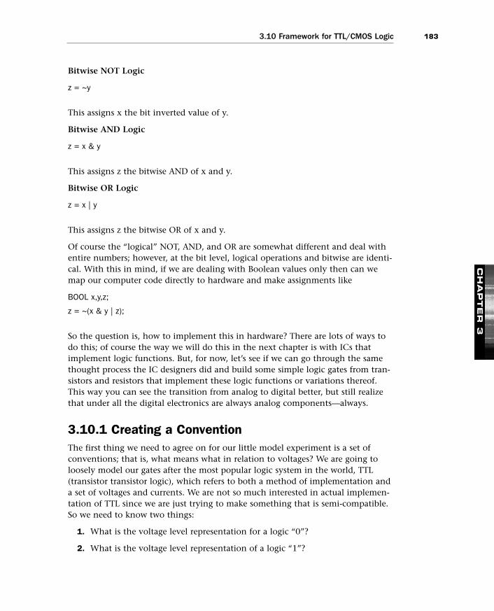
1833.10 Framework for TTL/CMOS Logic
Bitwise NOT Logic
z = ~y
This assigns x the bit inverted value of y.
Bitwise AND Logic
z = x & y
This assigns z the bitwise AND of x and y.
Bitwise OR Logic
z = x | y
This assigns z the bitwise OR of x and y.
Of course the “logical” NOT, AND, and OR are somewhat different and deal withentire numbers; however, at the bit level, logical operations and bitwise are identi-cal. With this in mind, if we are dealing with Boolean values only then can wemap our computer code directly to hardware and make assignments like
BOOL x,y,z;
z = ~(x & y | z);
So the question is, how to implement this in hardware? There are lots of ways todo this; of course the way we will do this in the next chapter is with ICs thatimplement logic functions. But, for now, let’s see if we can go through the samethought process the IC designers did and build some simple logic gates from tran-sistors and resistors that implement these logic functions or variations thereof.This way you can see the transition from analog to digital better, but still realizethat under all the digital electronics are always analog components—always.
3.10.1 Creating a ConventionThe first thing we need to agree on for our little model experiment is a set ofconventions; that is, what means what in relation to voltages? We are going toloosely model our gates after the most popular logic system in the world, TTL(transistor transistor logic), which refers to both a method of implementation anda set of voltages and currents. We are not so much interested in actual implemen-tation of TTL since we are just trying to make something that is semi-compatible.So we need to know two things:
1. What is the voltage level representation for a logic “0”?
2. What is the voltage level representation of a logic “1”?
CH
AP
TE
R 3
04_0672328208_ch03.qxd 11/15/05 2:48 PM Page 183

184 3.10 Framework for TTL/CMOS Logic
If you take a look at Figure 3.66 you will see a graph that shows the logic levelsfor a number of different logic families (courtesy of TI). We are only interested inthe TTL family for now, since it’s easiest to model. Referring to the TTL switchingstandard there are a number of demarcations on the graph; their meanings are asfollows:
VCC/GND—These are the “rails” of the power supply. VCC is the +5 supply and groundis 0V.
Vol—Voltage output low. This is the highest voltage a TTL gate will give when output alow.
Vil—Voltage input low. This is the highest voltage a TTL gate will detect as a low input.
Vih—Voltage input high. This is the lowest voltage a TTL gate will detect as a highinput.
Voh—Voltage output high. This is the lowest voltage a TTL gate is guaranteed to outputa high at.
CH
AP
TE
R 3
Logic levels for various switching logic families.
3.6
6
These seems a little weird, but the bottom line is that we need to consider twothings: what a TTL gate guarantees as low and high when it is an output, andwhat a TTL gate will detect as a low and high as an input. Between the text andthe figure you should be able to get it. Finally, the last assumption is that thedigital systems use +5V and that a high or “1” is +5 and a low or “0” is 0V ideally.With that in mind, we need to design our model “TTL” gates with thoseconstraints or at least close.
04_0672328208_ch03.qxd 11/15/05 2:48 PM Page 184

1853.10 Framework for TTL/CMOS Logic
3.10.1.1 Building an InverterThe inverter is the basis on 99% of all digital logic; if you can invert a signal thenyou can usually derive everything from there, so we will start with an inverter.Figure 3.67 depicts one possible design. The circuit operation is as follows. If weapply a 0V to the base at input X (Vin) then the transistor is OFF; in this case,there is no base current and thus no collector current (other than a very smallleakage current), therefore the output Z (Vout) will output nearly 5V. Thus, aninput of 0V (logic 0) outputs a 5V (logic 1). So far so good.
CH
AP
TE
R 3
10KΩ
0.6VIB
Y
Y
Vin
Vin
0V5V 1
0015V
X
X
[0v, +5v]Vout
Vout
IC (100)(440µA) = 44mA
Vout = 5V – (44mA)(100) = 0.6V
Vout = 0.2V
? But,Truth Table
100Ω
Q1
+5V NOT Gate
= 5 – 0.6
10K= 440µA
IC max = 5 – 0.2
100Ω = 48mA
A single transistor inverter.
3.6
7
Now, the hard part. Let’s apply a 5V (logic 1) to the base at X (Vin); when we dothis we turn ON the transistor and it starts conducting. When it does so the base-emitter junction wants to have a 0.6V drop across it; therefore, the base will be at
VB = VE + 0.6V
and since VE is at ground, VB = 0.6V. Therefore, we can compute IB as the voltagedrop over Rin divided by the resistance of Rin:
IB = (5V – 0.6V)/1KΩ = 4.4mA
We know that IC = hFE*IB roughly, and assuming an hFE of 100, we get an IC of
IC = 100*4.4mA = 44mA
However, this is only tentative; it may be less if this current violates one of thetransistor rules. Let’s see. With a collector current of 44mA, that means that thevoltage drop over Rout is
Vrout = 44mA*100Ω = 4.4V
04_0672328208_ch03.qxd 11/15/05 2:48 PM Page 185

186 3.10 Framework for TTL/CMOS Logic
Thus, the voltage at the collector VC and the output Z (Vout) is (5V-4.4V)=0.6V,which is above the requirement of 0.2V worst case for the collector above ground.Therefore, when we apply a signal of 5V (logic 1), we get a 0.6V output roughly(logic 0), and thus we have an inverter. Table 3.1 lists the inputs and outputs, soyou can confirm everything at once and assure yourself we have an inverter.
TABLE 3.1 Logic/Response Table for the “Model” TTL Inverter
Input Ouput
X (Vin) Z (Vout)
0 (0V) 1 (5.0V)
1 (5V) 0 (0.6V)
It’s almost perfect! And in reality, the output low will tend to be lower. Of course,we haven’t tested against the Vil, Vih values to see if we match the tolerance onthose constraints, but that’s not important. We at least have a TTL inverter thatgiven solid inputs outputs TTL outputs.
3.10.1.2 Building a NAND GateSo a single transistor can be used as an inverter. We can use this fact and thedesign now as a block and create other gates. Let’s create a NAND gate. Of coursewe could create an AND gate, but then we would have to invert its output, so aNAND is a little easier to implement.
CH
AP
TE
R 3
In digital electronics it is usually much more optimal to think in terms of NOT, NAND,and NOR rather than AND and OR. It takes a little getting used to, but in many casesa more optimal solution can be found by asking the opposite of the question ratherthan the question itself.
Since we have the analysis of the inverter under our belt, we can analyze theNAND gate without so much detail. Referring to Figure 3.68, there are two invert-ers more or less placed in series. The operation is as follows: When either inputX,Y or both are at 0V then one or both of the transistors are OFF. Therefore, thereis no appreciable collector current and the output Z will hang at approximately5.0V, a bit less; remember there is still a bit of leakage current even when the tran-sistor(s) are OFF. Thus, a logic 0,0 or 0,1, or 1,0 all result in an output of a logic 1at nearly 5.0V. This is looking like a NAND so far. The last case is when we turnboth transistors on with logic 1’s at X and Y. In this case, we turn both transistorson and then conduct hard; the collector voltages will each be 0.2V above therespective emitter’s for a worst case of 0.4V above ground at the final output nodeZ (Vout). So to reiterate when both inputs are driven to logic 1 (5V), the outputgoes to 0.4V or so, a logic 0.
04_0672328208_ch03.qxd 11/15/05 2:48 PM Page 186
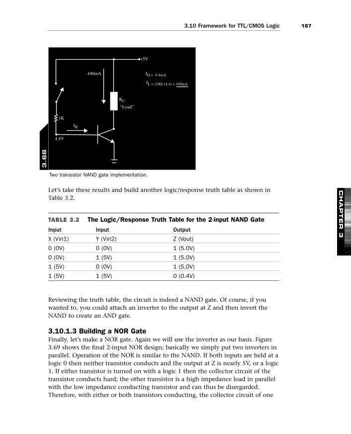
1873.10 Framework for TTL/CMOS Logic
Let’s take these results and build another logic/response truth table as shown inTable 3.2.
TABLE 3.2 The Logic/Response Truth Table for the 2-input NAND Gate
Input Input Output
X (Vin1) Y (Vin2) Z (Vout)
0 (0V) 0 (0V) 1 (5.0V)
0 (0V) 1 (5V) 1 (5.0V)
1 (5V) 0 (0V) 1 (5.0V)
1 (5V) 1 (5V) 0 (0.4V)
Reviewing the truth table, the circuit is indeed a NAND gate. Of course, if youwanted to, you could attach an inverter to the output at Z and then invert theNAND to create an AND gate.
3.10.1.3 Building a NOR GateFinally, let’s make a NOR gate. Again we will use the inverter as our basis. Figure3.69 shows the final 2-input NOR design; basically we simply put two inverters inparallel. Operation of the NOR is similar to the NAND. If both inputs are held at alogic 0 then neither transistor conducts and the output at Z is nearly 5V, or a logic1. If either transistor is turned on with a logic 1 then the collector circuit of thetransistor conducts hard; the other transistor is a high impedance load in parallelwith the low impedance conducting transistor and can thus be disregarded.Therefore, with either or both transistors conducting, the collector circuit of one
CH
AP
TE
R 3
IB
RC
IO = 4.4mA
“Load”
IL = (100) (4.4) = 440mA
440mA
4.4V
1K
+5V
Two transistor NAND gate implementation.
3.6
8
04_0672328208_ch03.qxd 11/15/05 2:48 PM Page 187
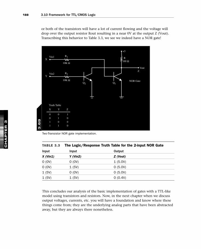
188 3.10 Framework for TTL/CMOS Logic
or both of the transistors will have a lot of current flowing and the voltage willdrop over the output resistor Rout resulting in a near 0V at the output Z (Vout).Transcribing this behavior to Table 3.3, we see we indeed have a NOR gate!
CH
AP
TE
R 3
X
0
1
0
1
1
0
0
1
Y
0
1
0
0
Z
Truth Table
NOR Gate
ZVout
100 Ω
R2
R1 R
+5
10K Ω
10K Ω
Vin2Y
Vin1X
Q1Q2
Two-Transistor NOR gate implementation.
3.6
9
TABLE 3.3 The Logic/Response Truth Table for the 2-input NOR Gate
Input Input Output
X (Vin1) Y (Vin2) Z (Vout)
0 (0V) 0 (0V) 1 (5.0V)
0 (0V) 1 (5V) 0 (5.0V)
1 (5V) 0 (0V) 0 (5.0V)
1 (5V) 1 (5V) 0 (0.4V)
This concludes our analysis of the basic implementation of gates with a TTL-likemodel using transistors and resistors. Now, in the next chapter when we discussoutput voltages, currents, etc. you will have a foundation and know where thesethings come from; they are the underlying analog parts that have been abstractedaway, but they are always there nonetheless.
04_0672328208_ch03.qxd 11/15/05 2:48 PM Page 188
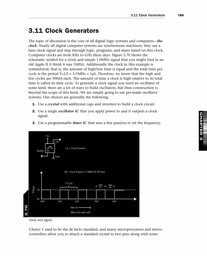
1893.11 Clock Generators
3.11 Clock GeneratorsThe topic of discussion is the core of all digital logic systems and computers—theclock. Nearly all digital computer systems are synchronous machines; they use abase clock signal and step through logic, programs, and states based on this clock.Computer clocks are from KHz to GHz these days. Figure 3.70 shows theschematic symbol for a clock and simple 1.0MHz signal that you might find in anold Apple II (I think it was 1MHz). Additionally the clock in this example issymmetrical; that is, the amount of high/low time is equal and the total time percycle is the period T=1/f = 1/1MHz = 1µS. Therefore, we know that the high andlow cycles are 500nS each. The amount of time a clock is high relative to its totaltime is called its duty cycle. To generate a clock signal you need an oscillator ofsome kind; there are a lot of ways to build oscillators, but their construction isbeyond the scope of this book. We are simply going to use pre-made oscillatorsystems. Our choices are generally the following:
1. Use a crystal with additional caps and inverters to build a clock circuit.
2. Use a single oscillator IC that you apply power to and it outputs a clocksignal.
3. Use a programmable timer IC that uses a few passives to set the frequency.
CH
AP
TE
R 3
1 Cycle
0µS 1µS 2µS 3µS 4µS
out
Gnd
Enable En
Vcc
(A.) Clock Symbol
(B.) Clock Signal at 1 MHZ 50–50 Duty
>|< >| |< 500ns
500ns
time (t)
Micro Seconds (µS)
Vol
tage
5V
0V
Clock and signal.
3.7
0
Choice 1 used to be the de facto standard, and many microprocessors and micro-controllers allow you to attach a standard crystal to two pins along with some
04_0672328208_ch03.qxd 11/15/05 2:48 PM Page 189

190 3.11 Clock Generators
bypass capacitors and the crystal will oscillate. Figure 3.71 shows an image of atypical crystal, but remember this is NOT an oscillator; it is only used as part of anoscillator circuit. Also, on the CD located at
CDROOT:\DATASHEETS\HC49U.pdf
CH
AP
TE
R 3
Typical crystal package.
3.7
1
you can find a datasheet with application notes for a common brand of crystals.Now, the pro of using an oscillator IC is that you only need a couple caps tobypass it if you are connecting it to a microprocessor or microcontroller, but ifyou want to build your own oscillator circuit that is based on a crystal, it’s muchharder, takes more parts, and is really hard to get working. Therefore, I never usecrystals anymore; they may be cheaper, but I prefer pre-made oscillator ICs asshown in Figure 3.72. Here you see a full can and half can design. They are thesame just with different packages. These are very simple to get working; you justbuy the oscillator frequency you want with the proper logic levels (most areTTL/CMOS and powered with +5), apply power to the corner pins, and the oscilla-tor roars into operation and puts out a perfect square wave.
Vcc
D1
1KΩ
0.1µF
8 5
413.58 MHz
Color Burst
OSC1
Oscillator circuit.
3.7
2
04_0672328208_ch03.qxd 11/15/05 2:48 PM Page 190
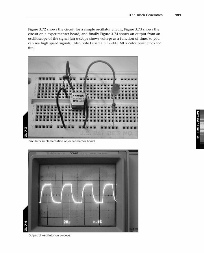
1913.11 Clock Generators
Figure 3.72 shows the circuit for a simple oscillator circuit, Figure 3.73 shows thecircuit on a experimenter board, and finally Figure 3.74 shows an output from anoscilloscope of the signal (an o-scope shows voltage as a function of time, so youcan see high speed signals). Also note I used a 3.579445 MHz color burst clock forfun.
CH
AP
TE
R 3
Oscillator implementation on experimenter board.
3.7
3
Output of oscillator on o-scope.
3.7
4
04_0672328208_ch03.qxd 11/15/05 2:48 PM Page 191

192 3.11 Clock Generators
The only problem with oscillators is that they are pretty expensive: around $2.00in high quantities (100 or more) to $5 in low quantities, 1 to 10. This is whypeople try to use crystals with analog components for oscillators, but the problemis that if you want to change the frequency of a crystal based oscillator, you mightnot be able to, since each crystal frequency requires slightly different de-couplingcaps that might be soldered into your board and non-removable, whereas with aoscillator IC you just pull it out of a socket and put another in. So my suggestionis to use oscillator ICs and not crystals. Also, on the CD located in
CDROOT:\DATASHEETS\ECS-2100_20Series.pdf
you can find a datasheet with application notes for a common brand of oscillators(notice some oscillators even have output enable pins, so you can tie 10 differentoscillators’ outputs together and then only enable one of them digitally!).
3.11.1 The 555 TimerNo electronics book can be without at least some mention of the 555 timer chip.The 555 is a standard 8-Pin DIP; Figure 3.75 shows an excerpt from the NationalSemiconductor datasheet for the 555 (LM555 is their part #). In any case, the 555is an amazing little device. It’s not the most accurate thing in the world, but it hasa lot of different modes of operation; astable, monoastable, time delay, etc.Basically, you can use it to create a constant clock with varying duty cycle, or oneshot pulse applications; the applications are really limitless. Referring to the appli-cations notes, the circuit for astable (free running oscillation) is shown on Page 7,Figure 4. A transcription of this is shown in Figure 3.75. So basically, you needtwo resistors Ra, Rb; a capacitor C; and a small bypass of 0.01µF to control theoutput of the chip. If you refer to Page 8, Figure 5 of the datasheet you will seethe math and analysis for the astable operation; it states that the frequency ofperiod and frequency of oscillation are
Equation 3.6: 555 timer period.
T = [0.693*(Ra + 2*Rb)*C]
and
F = 1/T = (1.44)/[(Ra + 2*Rb)*C]
And the duty cycle is D:
D = Rb / (Ra + 2*Rb)
So more or less you can use the equations to set the frequency of your oscillatorand desired duty cycle, but the cool part about it is that for testing purposes, the555 is wonderful, since if you replace Ra and Rb with a potentiometer (adjustable
CH
AP
TE
R 3
04_0672328208_ch03.qxd 11/15/05 2:48 PM Page 192
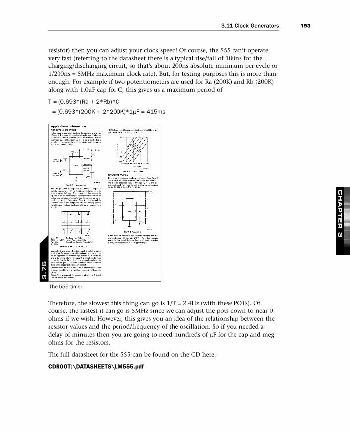
1933.11 Clock Generators
resistor) then you can adjust your clock speed! Of course, the 555 can’t operatevery fast (referring to the datasheet there is a typical rise/fall of 100ns for thecharging/discharging circuit, so that’s about 200ns absolute minimum per cycle or1/200ns = 5MHz maximum clock rate). But, for testing purposes this is more thanenough. For example if two potentiometers are used for Ra (200K) and Rb (200K)along with 1.0µF cap for C, this gives us a maximum period of
T = (0.693*(Ra + 2*Rb)*C
= (0.693*(200K + 2*200K)*1µF = 415ms
CH
AP
TE
R 3
The 555 timer.
3.7
5
Therefore, the slowest this thing can go is 1/T = 2.4Hz (with these POTs). Ofcourse, the fastest it can go is 5MHz since we can adjust the pots down to near 0ohms if we wish. However, this gives you an idea of the relationship between theresistor values and the period/frequency of the oscillation. So if you needed adelay of minutes then you are going to need hundreds of µF for the cap and megohms for the resistors.
The full datasheet for the 555 can be found on the CD here:
CDROOT:\DATASHEETS\LM555.pdf
04_0672328208_ch03.qxd 11/15/05 2:48 PM Page 193

194 Summary
SummaryThis chapter has been punishment for many I am sure; please forgive the techni-cal nature of it, but there is simply no way around it when discussing analog elec-tronics. The good news is you have the foundation you need to understand thefundamentals of what’s going on with capacitors, inductors, filters, transistors,and so forth. Additionally, the example design of TTL model gates with transistorswas actually pretty fun; who knows, maybe some glutton for punishment willmake an entire transistor based processor!
CH
AP
TE
R 3
04_0672328208_ch03.qxd 11/15/05 2:48 PM Page 194


![DYNAMICS OF A DISCRETE-TIME STOICHIOMETRIC ...hwang/DiscreteOptimalForaging.pdfstoichiometric optimal foraging model [15] with its discrete-time analog. We study the discrete-time](https://img.dokumen.tips/doc/110x75/60c2e22ddd4f9278ff1214c6/dynamics-of-a-discrete-time-stoichiometric-hwangdiscreteoptimalforagingpdf.jpg)