Embed Size (px)
DESCRIPTION
Analog Devices MT-99 tutorial
Citation preview

MT-099TUTORIAL
Analog Circuit Simulation
ANALOG CIRCUIT SIMULATION INTRODUCTION In recent years there has been much pressure placed on system designers to verify their designs with computer simulations before committing to actual printed circuit board layouts and hardware. Simulating complex digital designs is extremely beneficial, and very often, the prototype phase can be eliminated entirely. The same is not true for most analog circuits. While simulation can give a greater degree of confidence in the final design, completely bypassing the prototype phase in high-speed/high-performance analog or mixed-signal circuit designs can be very risky. For this reason, simulation should be accompanied with some amount of prototyping when dealing with analog circuits. Prototyping techniques are discussed in more detail in MT-100. The most popular analog circuit simulation tool is SPICE (Simulation Program with Integrated Circuit Emphasis), which is available in multiple forms for various computer platforms (see References 1 and 2). However, to achieve meaningful simulation results, designers need accurate models of many system components. The most critical of these are realistic models for integrated circuits. The op amp is a fundamental building block in nearly all analog circuits, and in the early 1990’s, Analog Devices developed an advanced op amp SPICE model, which is in fact still in use today (see References 3 and 4). Within this innovative open amplifier architecture, gain and phase response can be fully modeled, enabling designers to accurately predict ac, dc, and transient performance behavior. This modeling methodology has also been extended to include other devices such as in-amps, voltage references, and analog multipliers. The following discussion relates primarily to op amps and illustrates the fundamental principles
Understand Realistic Simulation GoalsEvaluate Available Models AccordinglyKnow the Capabilities for Each Competing Op Amp ModelFollowing Simulation, Breadboarding is Always Desirable and Necessary
Figure 1: Used Wisely, Simulation is a Powerful Design Tool
Figure 1 lists some major SPICE simulation objectives. The popularity of SPICE simulation has led to many op amp macromodel releases, which (ideally) software-mimic amplifier electrical performance. With numerous models available, several confusions are possible. There may be uncertainty as to what is/isn’t modeled, plus a basic question of model accuracy. All of these points are important, in order to place confidence in simulation results. So, verification of a model is important, checking it by comparison to the actual device performance conditions, before trusting it for serious designs.
Rev.0, 01/09, WK Page 1 of 15

MT-099
Of course, a successful first design step using an accurate op amp model by itself doesn’t necessarily guarantee totally valid simulations. A simulation based on incomplete information has limited value. All parts of a target circuit should be modeled, including the surrounding passive components, various parasitic effects, and temperature changes. Then, the circuit needs to be verified in the lab, by breadboarding and prototyping. A breadboard circuit is a quickly executed mockup of a circuit design using a semi-permanent lab platform, i.e., one which is less than final physical form. It is intended to show real performance, but without the total physical environment. A good breadboard can often reveal behavior not predicted by SPICE, either because of an incomplete model, external circuit parasitics, or numerous other reasons. However, by using SPICE along with intelligent breadboarding techniques, a circuit can be efficiently and quickly designed with reasonably good assurance of working properly on a prototype version, or even a final PCB. MACROMODEL VS. MICROMODEL The distinction between macromodel and micromodel is often unclear. A micromodel uses the actual transistor level and other SPICE models of an IC device, with all active and passive parts fully characterized according to the manufacturing process. In differentiating this type of model from a macromodel, some authors use the term device level model to describe the resulting overall op amp model (see Reference 5). Typically, a micromodel is used in the actual design process of an IC.
MACROMODEL
MICROMODEL
METHODOLOGY
Ideal ElementsModel Device
Behavior
Fully CharacterizedTransistor Level
Circuit
ADVANTAGES
Fast SimulationTime,
Easily Modified
Most CompleteModel
DISADVANTAGES
May Not Model AllCharacteristics
Slow SimulationPossible,
ConvergenceDifficulty,
Non-Availability
Figure 2: Differentiating Between the Macromodel and the Micromodel
A macromodel is a less complex way to simulate op amp performance. Taking into consideration final device performance, it uses ideal native SPICE elements to model observed behavior—as many as necessary. In developing a macromodel, a real device is measured in terms of lab and data sheet performance, and the macromodel is adjusted to match this behavior. Some aspects of performance may be sacrificed in doing this. Figure 2 compares the major pros and cons between macromodels and micromodels. There are advantages and disadvantages to both approaches. A micromodel can give a complete and accurate model of op amp circuit behavior under almost all conditions. But, because of a large number of transistors and diodes with non-linear junctions, simulation time is very long. Of course, manufacturers are also reluctant to release such models, since they contain proprietary
Page 2 of 15

MT-099
information. And, even though all transistors may be included, this isn’t a guarantee of total accuracy, as the transistor models themselves don’t cover all operational regions precisely. Furthermore, with a high node count, SPICE can have convergence difficulties, causing a failed simulation. This point would make a micromodel virtually useless for multiple amplifier active filters, for example. On the other hand, a carefully developed macromodel can produce both accurate results and simulation time savings. In more advanced macromodels such as the ADSpice model described below, transient and ac device performance can be closely replicated. Op amp non-linear behavior can also be included, such as output voltage and current swing limits. However, because these macromodels are still simplifications of real devices, all non-linearities aren’t modeled. For example, not all ADSpice models include common mode input voltage range, or noise (while more recent ones do). Typically, in model development parameters are optimized as may be critical to the intended application—for example, ac and transient response. Including every possible characteristic could lead to cumbersome macromodels that may even have convergence problems. Thus, ADSpice macromodels include those op amp behavior characteristics critical to intended performance for normal operating conditions, but not necessarily all non-linear behavior. THE ADSpice OP AMP MACROMODELS The basic ADSpice model was developed as an op amp macromodeling advance, and as an improved design tool for more accurate application circuit simulations. Since being introduced in 1990, it has become a standard op amp macromodel topology, as evidenced by industry adoption of the frequency shaping concepts (see References 6 and 7). Prior to about 1990, a dominant op amp model architecture was the Boyle model (see Reference 8). This macromodel, developed in the early 70’s, cannot accurately model higher speed amplifiers. The primary reason for this is that it has limited frequency shaping ability—only two poles and no zeroes. In contrast, the ADSpice model topology has a flexible and open architecture, allowing virtually unlimited pole and zero frequency shaping stages to be cascaded. This key difference provides much more accurate ac and transient response compared to the more simplistic Boyle model topology. An ADSpice model is comprised of three main portions, described as follows. The first of these is a combined input and gain stage, which will include transistor models as appropriate to the device being modeled (NPN or PNP bipolar, JFET, MOSFET, etc.). Next are the synthetic pole and zero stages, which are comprised of ideal SPICE native elements. There may be only a few of these or there may be many, dependent on the complexity of the op amp’s frequency response. Finally, there is an output stage, which couples the first two sections to the outside world. Before describing these sections in detail, it is important to realize that many variations upon what is shown below do in fact exist. This is due to not just differences from one op amp model to another, but also to evolutionary topology developments in op amp hardware, which in turn has led to corresponding modeling changes. For example, modern op amps often include either
Page 3 of 15

MT-099
rail-rail output or input stages, or both. Consequently more recent developments in the ADSpice models have addressed these issues, along with corresponding model developments. Furthermore, although the Boyle model and the original ADSpice models were designed to support voltage feedback op amp topologies, subsequent additions have added current feedback amplifier topologies. In fact, Reference 9 describes an ADSpice current feedback macromodel which appeared just shortly after the voltage feedback model of Reference 3. These current feedback macromodels are discussed in more detail below. ADSpice MACROMODEL: INPUT AND GAIN/POLE STAGES A basic ADSpice voltage feedback op amp macromodel input stage is shown in Figure 3. As noted, it uses what are (typically) the only transistors in the entire model, in this example the Q1-Q2 NPN pair, to the left on the diagram. These are needed to properly model an op amp's differential input stage characteristics. A basic tenet of this model topology is that this stage is designed for unity gain, by the proper choice of Q1-Q2 operating current and gain-setting resistors R3-R4 and R5-R6.
VD
IOS
CIN
+VS
-VS
I2IN+
R3
R5
1
R1
C2
Q1
+ -
Q2
R2
IN-
VOS
R6
R4
Input
gm1
R7 C3
EREF
INPUT STAGEGAIN = UNITY
OPEN LOOP GAIN/POLE STAGE GAIN = gm1 * R7
ENIN1
IN2
Figure 3: Input and Gain/Pole Stages of ADSpice Macromodel Although this example uses NPN transistors, the input stage is easily modified to use PNP bipolars, JFET, or MOSFET devices. The rest of the input stage uses simple SPICE elements such as resistors, capacitors, and controlled sources. The open-loop gain vs. frequency characteristics of the modeled op amp is provided by the gain stage, to the right in the diagram. Here controlled source gm1 senses the differential collector voltage VD from the input stage, converting this voltage to a proportional current. The gm1 output current flows in load resistor R7, producing a single ended voltage referenced to an internal
Page 4 of 15

MT-099
voltage, EREF. Typically, this voltage is derived as a supply voltage midpoint, and is used throughout the model. By simply making the gm1-R7 product equal to the specified gain of the op amp, this stage produces the entire open-loop gain of the macromodel. This design factor means that all other model stages operate at unity gain, a feature leading to significant flexibility in adding and deleting subsequent stages. This approach allows the quick synthesis of the complex ac characteristics typical of high performance, high speed op amps. In addition, this stage also provides the dominant pole of the amplifier’s ac response. The open-loop pole frequency is set by selection of capacitor C3, as noted in the diagram. ADSpice MACROMODEL: FREQUENCY SHAPING STAGES Following the gain stage of the macromodel is a variable but unlimited number of pole and/or zero stages, which in combination provide frequency response shaping. Typical topologies for these stages are as shown in the Figure 4 diagram. The stages can be either a single pole or a single zero, or combined pole/zero or zero/pole stages. All such stages have a dc transfer gain of unity, and a given amplifier type can have all or just a few of these stages, as may be require to synthesize its response.
ZERO STAGE
1R10R9R10 * E1 =+
R9
C5
E1R10
ZERO/POLE STAGEgm3 * R11 = 1
gm3R11
L1R12
POLE/ZERO STAGEgm4 * R13 = 1
gm4R14
C6R13
POLE STAGEgm2 * R8 = 1
EREF
EREF EREF
gm2
R8 C4
EREF
Figure 4: The Frequency Shaping Stages Possible within the ADSpice Model
The pole or zero frequency is set by the combination of the resistor(s) and capacitor, or resistor(s) and inductor, as may be the case. Because an infinite number of values are possible in SPICE, choice of RC values is somewhat arbitrary, and a wide range work. Early ADSpice
Page 5 of 15
MT-099
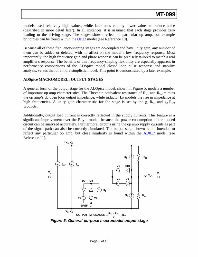
models used relatively high values, while later ones employ lower values to reduce noise (described in more detail later). In all instances, it is assumed that each stage provides zero loading to the driving stage. The stages shown reflect no particular op amp, but example principles can be found within the OP27 model (see Reference 10). Because all of these frequency-shaping stages are dc-coupled and have unity gain, any number of them can be added or deleted, with no affect on the model’s low frequency response. Most importantly, the high frequency gain and phase response can be precisely tailored to match a real amplifier's response. The benefits of this frequency-shaping flexibility are especially apparent in performance comparisons of the ADSpice model closed loop pulse response and stability analysis, versus that of a more simplistic model. This point is demonstrated by a later example. ADSpice MACROMODEL: OUTPUT STAGES A general form of the output stage for the ADSpice model, shown in Figure 5, models a number of important op amp characteristics. The Thevenin equivalent resistance of RO1 and RO2 mimics the op amp’s dc open loop output impedance, while inductor LO models the rise in impedance at high frequencies. A unity gain characteristic for the stage is set by the g7-RO1 and g8-RO2 products. Additionally, output load current is correctly reflected in the supply currents. This feature is a significant improvement over the Boyle model, because the power consumption of the loaded circuit can be analyzed accurately. Furthermore, circuits using the op amp supply currents as part of the signal path can also be correctly simulated. The output stage shown is not intended to reflect any particular op amp, but close similarity is found within the AD817 model (see Reference 11).
Figure 5: General-purpose macromodel output stage
g7 RO1
LO
D7 D8
D10
D9
g9
gSY
OO2 sL 2
RR IMPEDANCE OUTPUT ++= O1
VX VO
+VS
-VS
RO2g8
fSY V6
V5
V7 V8
EREF
Page 6 of 15

MT-099
With the recent advent of numerous rail-rail output stage op amps, a number of customized model topologies have been developed. This expands the ADSpice library to include rail-rail model behavior, matching op amp architectures using P and N MOSFET devices, as well as bipolar devices. Characteristically, a rail-rail output stage includes several key differentiating performance points. First and foremost is the ability to swing the op amp output to within a few mV of both supplies. A second point is the fact that such an output stage has a voltage gain greater than one, and a third is the relatively high output impedance (high as contrasted to traditional emitter follower outputs). Examples of several modeling approaches to rail-rail output stages are found in the ADI SPICE macromodel library. The OP295 (Reference 12) employs CMOS devices to realize a rail-rail output, while the OP284 (Reference 13) uses bipolar devices to the same end. The macromodels of the AD8031 and AD823 (References 14 and 15) use synthesis techniques to model rail-rail outputs. The AD8051/AD8052/AD8054, AD8552, and AD623 (References 16-18) utilize combinations of selected discrete device models and synthesis techniques, to realize rail-rail output operation for both op amp and instrumentation amplifier devices. In addition to rail-rail output operation, many modern op amps also feature rail-rail input stages. Such stages essentially duplicate, for example, an NPN-based differential stage with a complementary PNP stage, both stages operating in parallel. This allows the op amp to provide a CM range that includes both supply rails. This performance feature can also be accomplished within CMOS op amps, using both a P and N type MOS differential pairs. Model examples reflecting rail-rail input stages include the OP284, AD8031, and AD8552 (References 13, 14, and 17. ADSpice MACROMODEL: TRANSIENT RESPONSE The performance advantage of the multiple pole/zero stages is readily demonstrated in a transient pulse response test, as in Figure 6. This figure compares an actual OP249 op amp, the ADSpice model, and the Boyle model. It reveals the improved execution resulting from the unlimited number of poles and zeros in this model. Figure 6: A Pulse Response Comparison of an OP249 Follower (left) Model Favors
the ADSpice Model in Terms of Fidelity (center), but not the Boyle (right)
Page 7 of 15

MT-099
The difference is easily apparent from this transient analysis plot for a unity gain follower circuit. An OP249 amplifier was used, with the output connected to the inverting input, and a 260 pF capacitive load. As can be noted, this results in ringing, as seen in the op amp response (left). Note that the ADSpice model accurately predicts the amount of overshoot and frequency of the damped ringing (center). In contrast, the Boyle model (right) predicts about half the overshoot and significantly less ringing. ADSpice MACROMODEL: NOISE MODEL An important enhancement to the ADSpice model is the ability to realistically model noise performance of an op amp. The capability to model a circuit's noise in SPICE can be appreciated by anyone who has tried to analyze noise by hand. A complete analysis is an involved and tedious task that involves adding all the individual noise contributions from all active devices and all resistors, and referring them to the input. To aid this task, the ADSpice model was enhanced to include noise generators that accurately mimic the broadband and 1/f noise of an actual op amp. Conceptually, this involves first making an existing model noiseless, and then adding discrete noise generators, so as to emulate the target device. As noted earlier, all ADI models aren’t necessarily designed for this noise-accurate performance. Selected device models are designed for noise however, when their typical uses include low noise applications. The first step is an exercise in scaling down the model internal impedances. For example, by reducing the resistances in the pole/zero stages from a base resistance of 1E6 Ω to 1 Ω, total noise is reduced dramatically, as Figure 7 illustrates.
gm2
R9 C4
CASE"Noisy" "Noiseless"
R9 1x10⁶Ω 1Ωgm2 1x10⁻⁶ 1.0C4 159x10-15F 159x10-9FNoise 129nV/√Hz 129pV/√HzEREF
Figure 7: Towards Achieving Low Noise Operation, a First Design Step is the
Reduction of Pole/Zero Cell Impedances to Low Values For the "Noisy" column of the table, the noise from the pole stage shown with a large R9 resistor value is 129 nV/ Hz. But when this resistor is scaled down by a factor of 106, to 1 Ω , as in the "Noiseless" column, stage noise is 129 pV/ Hz. Note also that transconductance and capacitance values are also scaled by the same factor, maintaining the same gain and pole frequency. To make the model’s input stage noiseless, it is operated at a high current and with reduced load
Page 8 of 15

MT-099
resistances, making noise contributions negligible. Extending these techniques to the entire model renders it essentially noiseless. Once global noise reduction is achieved, independent noise sources are added, one for voltage noise and two for current noise. The basic noise source topology used is like Figure 8, and it can be set up to produce both voltage and current noise outputs.
DN1DNOISE1
RNOISE1VMEAS0
RNOISE2
FNOISE
EREF
VNOISE10.61
Figure 8: A Basic SPICE Noise Generator is formed with Diodes, Resistors,
and Controlled Sources Note that, within SPICE, semiconductor models can generate 1/f (flicker) noise. The noise generators use diodes such as DN1 to produce this portion of the noise, modeling the 1/f noise of the op amp. By properly specifying diode model parameters and bias voltage VNOISE1, the 1/f noise is tailored to match the op amp. The noise current from DN1 passes through a zero voltage source. Here VMEAS is being used as a measurement device, combining the 1/f noise from DN1 and the broadband noise from RNOISE1. RNOISE1 is selected for a value providing an appropriate broadband noise. The combined noise current in VMEAS is monitored by FNOISE, and appears as a voltage across RNOISE2. This voltage is then injected in series with one amplifier input via a controlled voltage source, such as EN of Figure 3 (see again). Either FNOISE or a controlled voltage source coefficient can be used for overall noise voltage scaling. Current noise generation is similar to the above, except that the RNOISE2 voltage producing resistor isn’t used, and two current-controlled sources drive the amplifier inputs. With all noise generators symmetrical about ground, dc errors aren’t introduced. ADSpice: CURRENT FEEDBACK AMPLIFIER MODELS As noted previously, a new model topology was developed for current feedback amplifiers, to accommodate their unique input stage structure (see Reference 9). The model uses a topology as shown in Figure 9 for the input and gain stages. The remaining model portions (not shown) contain multiple pole/zero stages and the output stage, and are essentially the same as voltage feedback amplifiers, described above.
Page 9 of 15

MT-099
Figure 9: Input and Gain Stages of Current Feedback Op Amp Macromodel The four bipolar transistor input stage resembles actual current feedback amplifiers, with a high impedance non-inverting input (+IN) and a low impedance inverting input (-IN). In current feedback amplifiers, the maximum slew rate is very high, because dynamic slew current isn’t limited to a differential pair tail current (as in voltage feedback op amps). In current feedback op amp designs, much larger amounts of error current can flow in the inverting input, as developed by the feedback network. Internally, this current flows in either Q3 or Q4, and charges compensation capacitor C3 via current mirrors. The current mirrors of the ADSpice model are actually voltage controlled current sources in the gain stage, G1 and G2. They sense voltage drops across input stage resistors R1 and R2, and translating this into a C3 charging current. By making the value of G1 and G2 equal to the R1- R2 reciprocal, the slew currents will be identical. By clamping the R1-R2 voltage drops via D1-V1 and D2-V2, the maximum current is limited, which thus sets the highest slew rate. Open loop gain or transresistance of the model is set by R5, and the open loop pole frequency by C3-R5 (as described previously, Figure 3 again). The output from across R5-C3 (node 12) drives the model’s succeeding frequency shaping stages, and EREF is again an internal reference voltage. One of the unique properties of current feedback amplifiers is that bandwidth is a function of the feedback resistor and the internal compensation capacitor, C3. The lower the feedback resistor, the greater the bandwidth, until a practical lower limit is reached, i.e., the value at which the part oscillates. As the model includes a low impedance inverting input, it accurately mimics real part behavior as RF is altered. Figure 10 compares the ADSpice model to the actual device for an AD811 video amplifier. As shown, the model accurately predicts the gain roll off at the much lower frequency for the 1kΩ feedback resistor as opposed to the 500 Ω resistor.
The current feedback amplifier input and gain stage is an enhancement to the ADSpice model that increases flexibility in modeling different op amp devices, and provides a net increase in design cycle speed.
Page 10 of 15

MT-099
Figure 10: Comparison of a Real AD811 Current Feedback Op Amp (left) with Macromodel (right) Shows Similar Characteristics as Feedback Resistance is
Varied MODELING PC BOARD PARASITICS PCB parasitics can have significant impact on a circuit's performance. This is especially true for high speed circuits. A few picofarads of capacitance on the input node can make the difference between a stable circuit and one that oscillates. Thus, these effects need to be carefully considered when simulating the circuit to achieve meaningful results. To illustrate the impact of PCB parasitics, the simple voltage follower circuit of Figure 11 (left) was built twice. The first time this was on a carefully laid out PCB, and the second time on a component plug-in type of prototype board. An AD847 op amp is used because of its 50 MHz bandwidth, which makes the parasitic effects much more critical (smaller C values will have a greater effect on results).
Figure 11: With Care and Low Parasitic Effects in the PCB Layout, Results of Lab
Testing (Center) and Simulation (Right) Can Converge
Page 11 of 15

MT-099
As the results above indicate, this circuit executed on a properly laid out PCB has a clean response with minor overshoot and ringing (center picture). The SPICE model results also closely agree with the real part, showing a corresponding simulation (right picture). On the other hand, the same circuit built on the plug-in prototype board shows distinctly different results. In general it shows much worse performance, due to the relatively high nodal capacitances around the op amp inputs, which degrade the square wave response to severe ringing, much less than full capability of the part. This is shown in Figure 12 in the center and right pictures, respectively. The voltage follower circuit on the left shows the additional capacitances as inherent to the prototype board. With this test circuit and corresponding analysis, there was (initially) no agreement between the poor lab test, and the parallel SPICE test. However, when the relevant PCB parasitic capacitances are included in the SPICE file, then the simulation results do agree with the real circuit, as noted in the right picture.
Figure 12: Without Low Parasitics, Lab Testing Results (Center) and Parallel Simulation (Right) Still Show Convergence—With A Poorly Damped Response
This example illustrates several key points. One, PCB parasitics can easily make a high speed circuit behave much differently from a simplistic SPICE analysis. Secondly, when the SPICE netlist is adjusted to more reasonably reflect the parasitic elements of a PCB, then the simulation results do compare with the actual lab test. Finally, a point that should be obvious, a clean PCB layout with minimal parasitics is critically important to high speed designs. To put this in a broader perspective, op amps of today are capable of operating to 1 GHz or more! Another interesting point is that the simulation can be used as a rough measure of the PCB layout design. If the simulation, without any parasitics, agrees with the PCB, then there is a reasonable assurance that PCB is well laid out. Parasitic PCB elements are not the only area that may cause differences between the simulation and the breadboard. A circuit may exhibit non-linear behavior during power-on that will cause a device to lock-up. Or, a device may oscillate due to insufficient power supply decoupling or lead inductance. SPICE circuits need no bypassing, but real world ones always do! It is, practically
Page 12 of 15

MT-099
speaking, impossible to anticipate all normal or abnormal operating conditions to which an amplifier might be subjected. Thus, it is always important that circuits be prototyped and thoroughly checked in the lab. Careful forethought in these stages of design helps minimize any unknown problems from showing up when the final PCBs are manufactured. OTHER ADI DESIGN AND SIMULATION TOOLS Analog Devices has a large number of useful design tools located at the Design Center on the ADI website. Among them are the following tools which relate to simulation discussed in this tutorial. ADIsimOpAmp is an on-line tool to help with the selection, evaluation and troubleshooting of voltage feedback operational amplifiers (Op-Amps). It has two modes of Evaluation:
1. "APET" Mode (Amplifier Parametric Evaluation Tool) Uses National Instruments LabVIEW® along with typical parametric data to mathematically model the general behavior of a selected amplifier. It allows a user to choose an amplifier, quickly configure a circuit, apply a signal, and evaluate its general performance.
2. "SPICE" Mode Uses the MultiSIM9® SPICE simulation engine allowing the user to
perform additional testing in the SPICE environment. ADIsimOpAmp is useful for quickly selecting and checking an amplifier's parametric performance such as gain bandwidth, slew rate, input/output range, differential voltages, gain error, load current, possible stability issues and dc errors. The APET mode is limited to first-order approximations, and additional evaluation should be performed using SPICE simulation and hardware testing. The basic simulation process using the APET mode is as follows:
1. Select the Circuit 2. Enter the Circuit Component Values 3. Select and Enter the Input Signal Parameters 4. Select the Amplifier to be Evaluated 5. Parametric Search 6. Amplifier Wizard 7. Suggest Amplifier (Reverse Search-See Below) 8. Analyze the Amplifier’s Response 9. Run Model 10. View Results
The "Suggest Amplifier" function uses the entered circuit requirements to perform parametric calculations on all amplifiers located in the data base. Once the calculations are complete a list of
Page 13 of 15

MT-099
parts from best to least is generated. If an amplifier that meets all requirements can't be found, the search will suggest components that are close. With National Instrument's Multisim™ Analog Devices® Edition, ADI and the NI Electronics Workbench Group equip circuit board designers with a free, downloadable version of NI Multisim tailored for evaluating ADI components. Avoid costly and time consuming prototyping work by using this easy-to-use interactive SPICE simulator. With the NI Multisim Analog Devices Edition, engineers can:
1. Build simulated component evaluation circuits to quickly assess behavior of over 800 Analog Devices operational amplifiers, switches and voltage references
2. Examine the unit under test in the intended circuit topology with up to 25 components 3. Use built-in instruments and analyses including oscilloscopes and worst-case analysis 4. Swap components easily to pinpoint best design options 5. Link to the Analog Devices Design Center for more online evaluation tools 6. Instantly access product pages and datasheets of each Analog Devices component 7. Upgrade to a full edition of NI Multisim to complete designs and transfer to board layout
with NI Ultilboard REFERENCES: 1. L. W. Nagel, "SPICE2: A Computer Program to Simulate Semiconductor Circuits," May 1975, UCB/ERL
M75/520, Univ. of California, Berkeley, CA, 94720. 2. Andrei Vladimirescu, K.Zhang, A.R.Newton, D.O.Pederson, "SPICE Version 2G User’s Guide," August 1981,
Department of Electrical Engineering and Computer Sciences, Univ. of California, Berkeley, CA, 94720. 3. Mark Alexander, Derek Bowers, "SPICE-Compatible Op Amp Macromodels," EDN, February 15, 1990 and
March 1, 1990 (available as Analog Devices, Inc. AN-138). 4. Joe Buxton, "Analog Circuit Simulation," Chapter 13 of Amplifier Applications Guide, 1992, Analog Devices,
Inc., Norwood, MA, ISBN 0-916550-10-9. 5. Andrei Vladimerescu, The SPICE Book, John Wiley & Sons, New York, 1994, ISBN 0-471-60926-9. 6. "Development of an Extensive SPICE Macromodel for "Current-Feedback" Amplifiers," National
Semiconductor AN-840, July 1992. 7. David Hindi, "A SPICE Compatible Macromodel for CMOS Operational Amplifiers," National Semiconductor
AN-856, September 1992. 8. Boyle, et al, "Macromodelling of Integrated Circuit Operational Amplifiers," IEEE Journal of Solid State
Circuits, Vol. SC-9, no.6, December 1974. 9. Derek Bowers, Mark Alexander, Joe Buxton, "A Comprehensive Simulation Macromodel for ‘Current
Feedback’ Operational Amplifiers," IEE Proceedings, Vol. 137, Pt. G, # 2, April 1990. 10. OP27 op amp macromodel, Rev B, Analog Devices, Inc., SPICE model library, December 1990. 11. AD817 op amp macromodel, Rev A, Analog Devices, Inc., SPICE model library, November 1992.
Page 14 of 15

Page 15 of 15
MT-099 12. OP295 op amp macromodel, Rev 2.0, Analog Devices, Inc., SPICE model library, July, 2008. 13. OP284 op amp macromodel, Rev B, Analog Devices, Inc., SPICE model library, November 1995. 14. AD8031A op amp macromodel, Rev C, Analog Devices, Inc., SPICE model library, August 1996. 15. AD823AN op amp macromodel, Rev C, Analog Devices, Inc., SPICE model library, April 1997. 16. AD8051/AD8052/AD8054 op amp macromodel, Rev 0, Analog Devices, Inc., SPICE model library, September
1998. 17. AD8552 op amp macromodel, Rev 1.0, Analog Devices, Inc., SPICE model library, July, 1999. 18. AD623 in-amp macromodel, Rev B, Analog Devices, Inc., SPICE model library, September 2000. 19. PSpice® Simulation software, http://www.cadence.com/products/orcad/pages/default.aspx . 20. Hank Zumbahlen, Basic Linear Design, Analog Devices, 2006, ISBN: 0-915550-28-1. Also available as Linear
Circuit Design Handbook, Elsevier-Newnes, 2008, ISBN-10: 0750687037, ISBN-13: 978-0750687034. Chapter 12
21. Walter G. Jung, Op Amp Applications, Analog Devices, 2002, ISBN 0-916550-26-5, Chapter 7. Also available
as Op Amp Applications Handbook, Elsevier/Newnes, 2005, ISBN 0-7506-7844-5. Chapter 7. 22. Walt Kester, High Speed System Applications, Analog Devices, 2006, ISBN-10: 1-56619-909-3, ISBN-13: 978-
1-56619-909-4, Part 4. Copyright 2009, Analog Devices, Inc. All rights reserved. Analog Devices assumes no responsibility for customer product design or the use or application of customers’ products or for any infringements of patents or rights of others which may result from Analog Devices assistance. All trademarks and logos are property of their respective holders. Information furnished by Analog Devices applications and development tools engineers is believed to be accurate and reliable, however no responsibility is assumed by Analog Devices regarding technical accuracy and topicality of the content provided in Analog Devices Tutorials.