Embed Size (px)
Citation preview

AN62-1
Application Note 62
October 1994
Data Acquisition Circuit CollectionKevin R. Hoskins
INTRODUCTION
This application note features 8-, 10-, and 12-bit dataacquisition components in various circuit configurations.The circuits include battery monitoring, temperature sens-ing, isolated serial interfaces, and microprocessor andmicrocontroller serial and parallel interfaces. Also in-cluded are voltage reference circuits (Application Note 42contains more voltage reference circuits).
Additional circuit information is located in the informationreferences listed in the Circuit Index. Each informationreference refers to either an application note (example:AN42 = Application Note 42), a data sheet (example:LTC®1292 DS = LTC1292 Data Sheet), or a design note(example: DN66 = Design Note 66).
and LTC are registered trademarks and LT is a trademark of Linear Technology Corporation.
General Analog-to-Digital Application CircuitsTwo-Quadrant 150kHz Bandwidth Analog Multiplier ....................................................... Figure 1 ....... AN62-3 .................. LTC1099 DSInfinite Hold-Time Sample-and-Hold (tACQ = 240ns) ....................................................... Figure 2 ....... AN62-3 .................. LTC1099 DSFour-Quadrant 250kHz Bandwidth Analog Multiplier ....................................................... Figure 3 ....... AN62-4Demodulating a Signal Using Undersampling ................................................................. Figure 4 ....... AN62-4 .................. LTC1257 DSComplete 100ps Resolution ∆Time Circuit with “Bow” Correction .................................. Figure 5 ....... AN62-5 .................. LTC1282 DSSingle 5V 12-Bit Temperature Control System with Shutdown........................................ Figure 6 ....... AN62-6 .................. LTC1257 DSWeight Scale .................................................................................................................... Figure 7 ....... AN62-6 ......... LTC1091/2/3/4 DSAuto-Ranging 8-Channel 12-Bit Data Acquisition System with Shutdown ....................... Figure 8 ....... AN62-7 .................. LTC1257 DSAnalog-to-Digital Battery Monitoring Application CircuitsMicropower Battery Voltage Monitor .............................................................................. Figure 9 ....... AN62-8 ............... LTC1096/8 DS0A to 2A Battery Current Monitor Draws Only 70µA ........................................................ Figure 10 ..... AN62-8 ............... LTC1096/8 DSLTC1297 Data Acquisition System Micropower Battery Current Monitor ........................ Figure 11 ..... AN62-9Temperature Sensing and ConversionCurrent Output Silicon Sensor Thermometer Driving 10-Bit Analog-to-Digital
Converter Covers –55°C to 125°C with 0.2°C Resolution ........................................ Figure 12 ..... AN62-9 ......... LTC1091/2/3/4 DSThermistor-Based Temperature Measurement System Covers 20°C to 40°C
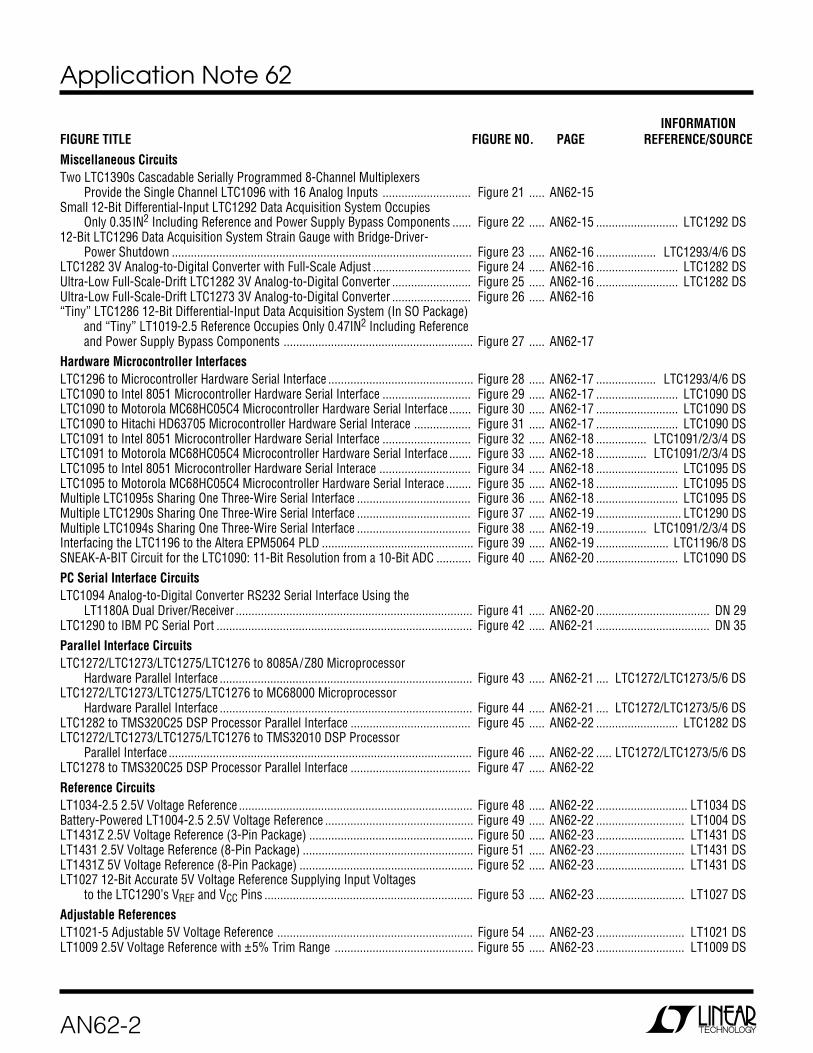
and 0°C to 100°C with 0.25°C Accuracy .................................................................. Figure 13 ..... AN62-10 ........ LTC1091/2/3/4 DSDigitally Linearized Platinum RTD Signal Conditioner ..................................................... Figure 14 ..... AN62-10 ........ LTC1091/2/3/4 DSFurnace Exhaust Gas Temperature Monitor Covers 0°C to 500°C
and Has Low Supply Detection ................................................................................ Figure 15 ..... AN62-11 ........ LTC1091/2/3/4/DSIsolated InterfacesFloating Analog-to-Digital Conversion System Powered by Capacitor Charge Pump ...... Figure 16 ..... AN62-11 .............. LTC1096/8 DSMicropower Serial 10-Bit Data Acquisition System with 500V Opto-Isolated
Communication ....................................................................................................... Figure 17 ..... AN62-12 ........ LTC1091/2/3/4 DSOpto-Isolated Temperature Monitor ................................................................................ Figure 18 ..... AN62-13 ................. LTC1292 DSBattery-Powered Digital Thermometer Transmits Over RF-Link ...................................... Figure 19 ..... AN62-13LTC1092 10-Bit Analog-to-Digital Converter Receives Power and
Transmits Data Over Two Transformer-Isolated Lines ............................................. Figure 20 ..... AN62-14 ............................ DN19
CIRCUIT INDEXINFORMATION
FIGURE TITLE FIGURE NO. PAGE REFERENCE/SOURCE
Application Note 62
AN62-2
INFORMATIONFIGURE TITLE FIGURE NO. PAGE REFERENCE/SOURCEMiscellaneous CircuitsTwo LTC1390s Cascadable Serially Programmed 8-Channel Multiplexers
Provide the Single Channel LTC1096 with 16 Analog Inputs ............................ Figure 21 ..... AN62-15Small 12-Bit Differential-Input LTC1292 Data Acquisition System Occupies
Only 0.35IN2 Including Reference and Power Supply Bypass Components ...... Figure 22 ..... AN62-15 .......................... LTC1292 DS12-Bit LTC1296 Data Acquisition System Strain Gauge with Bridge-Driver-
Power Shutdown ............................................................................................... Figure 23 ..... AN62-16 ................... LTC1293/4/6 DSLTC1282 3V Analog-to-Digital Converter with Full-Scale Adjust ............................... Figure 24 ..... AN62-16 .......................... LTC1282 DSUltra-Low Full-Scale-Drift LTC1282 3V Analog-to-Digital Converter ......................... Figure 25 ..... AN62-16 .......................... LTC1282 DSUltra-Low Full-Scale-Drift LTC1273 3V Analog-to-Digital Converter ......................... Figure 26 ..... AN62-16“Tiny” LTC1286 12-Bit Differential-Input Data Acquisition System (In SO Package)
and “Tiny” LT1019-2.5 Reference Occupies Only 0.47IN2 Including Referenceand Power Supply Bypass Components ............................................................ Figure 27 ..... AN62-17
Hardware Microcontroller InterfacesLTC1296 to Microcontroller Hardware Serial Interface .............................................. Figure 28 ..... AN62-17 ................... LTC1293/4/6 DSLTC1090 to Intel 8051 Microcontroller Hardware Serial Interface ............................ Figure 29 ..... AN62-17 .......................... LTC1090 DSLTC1090 to Motorola MC68HC05C4 Microcontroller Hardware Serial Interface ....... Figure 30 ..... AN62-17 .......................... LTC1090 DSLTC1090 to Hitachi HD63705 Microcontroller Hardware Serial Interace .................. Figure 31 ..... AN62-17 .......................... LTC1090 DSLTC1091 to Intel 8051 Microcontroller Hardware Serial Interface ............................ Figure 32 ..... AN62-18 ................ LTC1091/2/3/4 DSLTC1091 to Motorola MC68HC05C4 Microcontroller Hardware Serial Interface ....... Figure 33 ..... AN62-18 ................ LTC1091/2/3/4 DSLTC1095 to Intel 8051 Microcontroller Hardware Serial Interace ............................. Figure 34 ..... AN62-18 .......................... LTC1095 DSLTC1095 to Motorola MC68HC05C4 Microcontroller Hardware Serial Interace ........ Figure 35 ..... AN62-18 .......................... LTC1095 DSMultiple LTC1095s Sharing One Three-Wire Serial Interface .................................... Figure 36 ..... AN62-18 .......................... LTC1095 DSMultiple LTC1290s Sharing One Three-Wire Serial Interface .................................... Figure 37 ..... AN62-19 ........................... LTC1290 DSMultiple LTC1094s Sharing One Three-Wire Serial Interface .................................... Figure 38 ..... AN62-19 ................ LTC1091/2/3/4 DSInterfacing the LTC1196 to the Altera EPM5064 PLD ................................................ Figure 39 ..... AN62-19 ....................... LTC1196/8 DSSNEAK-A-BIT Circuit for the LTC1090: 11-Bit Resolution from a 10-Bit ADC ........... Figure 40 ..... AN62-20 .......................... LTC1090 DSPC Serial Interface CircuitsLTC1094 Analog-to-Digital Converter RS232 Serial Interface Using the
LT1180A Dual Driver/Receiver ........................................................................... Figure 41 ..... AN62-20 .................................... DN 29LTC1290 to IBM PC Serial Port ................................................................................. Figure 42 ..... AN62-21 .................................... DN 35Parallel Interface CircuitsLTC1272/LTC1273/LTC1275/LTC1276 to 8085A/Z80 Microprocessor
Hardware Parallel Interface ................................................................................ Figure 43 ..... AN62-21 .... LTC1272/LTC1273/5/6 DSLTC1272/LTC1273/LTC1275/LTC1276 to MC68000 Microprocessor
Hardware Parallel Interface ................................................................................ Figure 44 ..... AN62-21 .... LTC1272/LTC1273/5/6 DSLTC1282 to TMS320C25 DSP Processor Parallel Interface ...................................... Figure 45 ..... AN62-22 .......................... LTC1282 DSLTC1272/LTC1273/LTC1275/LTC1276 to TMS32010 DSP Processor
Parallel Interface ................................................................................................ Figure 46 ..... AN62-22 ..... LTC1272/LTC1273/5/6 DSLTC1278 to TMS320C25 DSP Processor Parallel Interface ...................................... Figure 47 ..... AN62-22Reference CircuitsLT1034-2.5 2.5V Voltage Reference .......................................................................... Figure 48 ..... AN62-22 ............................. LT1034 DSBattery-Powered LT1004-2.5 2.5V Voltage Reference ............................................... Figure 49 ..... AN62-22 ............................ LT1004 DSLT1431Z 2.5V Voltage Reference (3-Pin Package) .................................................... Figure 50 ..... AN62-23 ............................ LT1431 DSLT1431 2.5V Voltage Reference (8-Pin Package) ...................................................... Figure 51 ..... AN62-23 ............................ LT1431 DSLT1431Z 5V Voltage Reference (8-Pin Package) ....................................................... Figure 52 ..... AN62-23 ............................ LT1431 DSLT1027 12-Bit Accurate 5V Voltage Reference Supplying Input Voltages
to the LTC1290’s VREF and VCC Pins .................................................................. Figure 53 ..... AN62-23 ............................ LT1027 DSAdjustable ReferencesLT1021-5 Adjustable 5V Voltage Reference .............................................................. Figure 54 ..... AN62-23 ............................ LT1021 DSLT1009 2.5V Voltage Reference with ±5% Trim Range ............................................ Figure 55 ..... AN62-23 ............................ LT1009 DS

AN62-3
Application Note 62
GENERAL ANALOG-TO-DIGITAL APPLICATION CIRCUITS
INFORMATIONFIGURE TITLE FIGURE NO. PAGE REFERENCE/SOURCE
–
+
NC
5V
3MHZ OSC
OUTCLK
N/C
74LS90
0.1µF
0.1µF
4.7µF
0.1µF 10µF
0.1µF
1
2
3
4
5
6
7
14
13
12
11
10
9
8
÷10 = 300kHz
5V
(VIN) 0V TO 5V ANALOG INPUT
5VREF15VIN
(VIN2) +10V TO –10V ANALOG INPUT
1
2
3
4
5
6
7
8
9
10
1
2
3
4
5
6
7
8
9
10
11
12
DB0
DB1
DB2
DB3
WR/RDY
MODE
RD
INT
GND
OUT
AGND
DB7
DB6
DB5
DB4
CS
REF+
REF–
20
19
18
17
16
15
14
13
12
11
24
23
22
21
20
19
18
17
16
15
14
13
5V VCC
CS
WR1
GND
DI5
DI4
DI3
DI2
DI1
DI0
VREF
RFB
5V
NC
LTC1099
LT1019-5
CS AND RD LOW
4 DB0 TO DB3
DAC 12084
DB4 TO
DB7
= ANALOG GROUND
= DIGITAL GROUND
= BUS
8 12V
812
34 5
67
25k
15 15V
OUTPUT
–15V
50k OFFSET NULL 15V
10pF
LT1122
AN62 F01
WR2
XFER
DI6
DI7
DI8
DI9
DI10
DI11
IOUT2
IOUT1
BYTE1/ BYTE2
+
VIN1
7DB7
DB6
DB5
DB4
DB3
DB2
DB1
DB0
LTC1099
AM6012
B1
B2
B3
B4
B5
B6
B7
B8
17
16
15
14
5
4
3
2
18
3LT1122
4
7
6
2
19
–15V
1715
201412 20
1
2
3
4
5
6
7
8
6
8
13
10 11
SAMPLE
HOLD
AN62 F02
REF +
10k
2.5k
10k
V+
15V5.000V
REF– V–
IO
VOUT
IO
Figure 2. Infinite Hold Time Sample-and-Hold (tACQ = 240ns)
Figure 1. Two-Quadrant 150kHz Bandwidth Analog Multiplier
AppendicesAnalog-to-Digital/Digital-to-Analog Converter Selection Guides .................................. Appendix A ...... AN62-24Voltage Reference Selection Guide .............................................................................. Appendix B ...... AN62-28

Application Note 62
AN62-4
AIN LTC1275D11
D0
455kHz AMPLITUDE
MODULATED INPUT
RD RD
–5V
227.5kHz SAMPLE RATE
5V
AN62 F04a*
DATA OUTPUT
Figure 4. Demodulating a Signal Using Undersampling
1
2
19
22
18
20
21
24
23
3
17
12
4
5
6
7
8
9
10
11
13
14
15
16
10
13
14
11
12
21
22
21
CS
23
24
3
15
16
17
18
19
20
4
5
6
7
8
9
AIN
VREF
CONVST
BUSY
SHDN
RD
CS
AVDD
VSS
AGND
DVDD
DGND
D11
D10
D9
D8
D7
D6
D5
D4
D3
D2
D1
D0
VREF
IOUT1
IOUT2
RFB
GND
XFER
WR2
WR1
CS
BYTE1/BYTE2
VCC
GND
D11
D10
D9
D8
D7
D6
D5
D4
D3
D2
D1
D0
–5V ≤ VIN1 ≤ 5V
SAMPLE CLOCK (fSAMPLE ≤ 500kHz)
VA+ = 5V
VA– = –5V
VD+ = 5V
VA+ = POSITIVE ANALOG SUPPLY VOLTAGE
VA– = NEGATIVE ANALOG SUPPLY VOLTAGE
VD+ = DIGITAL SUPPLY VOLTAGE
LTC1278
0.1µF
0.1µF
0.1µF
VOUT
15V
AN62 F03
15V
–15V
–
+LT1122
0.1µF
0.1µF
10µF
0.1µF
0.1µF
DAC1208
–10V ≤ VIN2 ≤ 5V
= ANALOG GROUND
= DIGITAL GROUND
+
Figure 3. Four-Quadrant 250kHz Bandwidth Analog Multiplier
5µs/DIVAN62 F04b
455kHzAM SIGNAL
MODULATEDBY –6dB, 5kHz
SINEWAVE
DEMODULATED5kHz OUTPUT
SINEWAVE1V/DIV
1V/DIV

AN62-5
Application Note 62
VSS GND
AIN
REFOUT VDD
LTC1282
CS RD BUSY
12-BIT DATA OUTPUT
10µF
20k
200k
250pF POLYSTYRENE
430Ω
65Ω
3.3V
74HC03
65Ω
45.3Ω
45.3Ω
1N457
LM134
D
CLK
Q
QCLR
D
CLK
Q
QCLR
1k3.3V
3.3V
START↑
3.3V
STOP↑
DATA LATCH SIGNAL
10µF
1k
5V
100k
1N4148
0.001µF
10k
1N457
74HC74
10pF
1k 1N4148
100pF
10k
AN62 F05a
+
+
2N5771
2N23692N2369
RAMP 500mV/DIV
50ns/DIVTHE PHOTO SHOWS THE START, STOP AND RAMP WAVE-FORMS FOR A HALF SCALE, 200ns INPUT. THE RAMP REACHES2.5V IN 400ns FOR A FULL-SCALE ADC INPUT. THE 4096CODES SPREAD OVER 400ns EQUATE TO 100ps PER LSB.
AN62 F05c
STOP 5V/DIV
START 5V/DIV
Figure 5. Complete 100ps Resolution ∆Time Circuit with “Bow” Correction
∆TIME (ns)0
∆TIM
E LI
NEAR
ITY
ERRO
R (n
s)
1.0
0.8
0.6
0.4
0.2
0
–0.2
–0.4
–0.6
–0.8
–1.0400
AN62 F05b
100 200 300 500

Application Note 62
AN62-6
AN62 F06
µP
CLK
LOAD
DOUTGND
VCCVREF
VOUT LTC1257 DAC
CS
DOUT
CLK
VCC–IN
+IN
GND
5V
LTC1297 ADC
10µF
VREF
1µF
10k100k
–
+100k
47k
0.1µFVIN
GND COMM
LT1025A
1µF
1k
1µF
–+
2N3906
LTC1050
74k
CONTROL OUTPUT
DAC LOAD
DATA
CLK
CS/ POWER DOWN
DIN
J
+
Figure 6. Single 5V 12-Bit Temperature Control System with Shutdown
Figure 7. Weight Scale
NCI 3220 SCALE PLATFORM1k
VIOLET
BLACK, BLUE
FS ADJ
4.7µF
4.7µF
2µF
2k 9.09k
2.15M
2.15M2k
3
7
6.2Ω 4.75k
AN62 F07
5.23k
5V
5V
S1
8 5
64
2
1
1k
10k GREEN–
WHITE+
RED, YELLOW
MC68HC05PB0
PC2 MISO SCK
PA7
CLK
DOUT
MOTOR DRIVER
–
+
+
+
–
+LT1013
LTC1092
LT1013
CS

AN62-7
Application Note 62
AN62 F08
CLK
LOAD
DOUTGND
VREFVCC
VOUT
µP
DAC2 LTC1257
NOTE: THE µP SETS THE LTC1296’s FULL-SCALE AND ZERO-SCALE MAGNITUDES WITH THE CODE APPLIED TO DAC1 AND DAC2, RESPECTIVELY.
CLK
LOAD
DOUTGND
VREFVCC
VOUTDAC1
LTC1257
CS
DOUT
CLK
DIN
VCCCH0
CH7
COM
REF+ SSOREF–
5V22µF
8 ANALOG INPUT CHANNELS
74HC04
50k50k5V
0.1µF
100Ω
0.1µF
100Ω
0.1µF
LTC1296
DIN
DIN
2N3906
+
Figure 8. Auto-Ranging 8-Channel 12-Bit Data Acquisition System with Shutdown

Application Note 62
AN62-8
–
+
–
+
0.2Ω FOR 2A FULL SCALE 0.2Ω FOR 0.2A FULL SCALE
1/2 LT1178
1/2 LT1178
750k
73.2k
24.9k
3V TO 6V
0.1µF
0.1µF
TO µP
AN62 F10
750k
470k
470kLT1004-1.2
L O A D
LO BATTERY
LTC1096
CS
+IN
–IN
GND
VCC
CLK
DOUT
VREF
Figure 10. 0A to 2A Battery Current Monitor Draws Only 70µA
–IN
75k
3Ω
+INVCC
VREF GND
LTC1096
BATTERY MONITOR INPUT 8V TO 16V
CS
CLOCK
DOUT
LT1004-1.2
3V
AN62 F09
0.1µF266k
100k
1µF
0.1µF
Figure 9. Micropower Battery Voltage Monitor
ANALOG-TO-DIGITAL BATTERY MONITORING APPLICATION CIRCUITS

AN62-9
Application Note 62
11.5k0.1µF
226Ω
LM134 OR OTHER 1µA/°K SENSOR
LT1019-2.5
5V
+ +
9V
10µF4.7µF
3Ω
AN62 F12
TO MCU
LTC1092
CS
+IN
–IN
GND
VCC
SCLK
DOUT
VREF
Figure 12. Current Output Silicon Sensor Thermometer Driving 10-Bit Analog-to-DigitalConverter Covers –55°C to 125°C with 0.2°C Resolution
TEMPERATURE SENSING AND CONVERSION
Figure 11. LTC1297 Data Acquisition System Micropower Battery Current Monitor
–
+
CS
+IN
–IN
GND
VCC
CLK
DOUT
VREF
510k 6V TO 12V
0.005Ω 2A FULL SCALE
3k
750k
0.1µF
10Ω
1/2 LTC1047
1µF
0.33µF
1N4148
5VIN
GND
L O A D
OUT
SHDN
LT1121
LTC1297
22µF TANT
0.1µF
LT1004-2.5
20M
LO BATTERY
TO µP–
+1/2
LTC1047
AN62 F11
470k
100k
+
Application Note 62
AN62-10
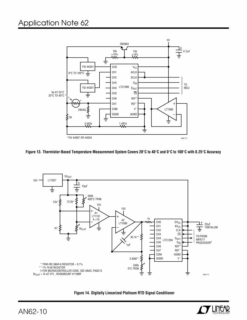
Figure 14. Digitally Linearized Platinum RTD Signal Conditioner
Figure 13. Thermistor-Based Temperature Measurement System Covers 20°C to 40°C and 0°C to 100°C with 0.25°C Accuracy
AN62 F14
1k
22µF TANTALUM
CH0 CH1 CH2 CH3 CH4 CH5 CH6 CH7 COM DGND
DVCC AVCC CLK CS
DOUT DIN
REF+ REF–
AGND V–
LTC1294
–
+
TO/FROM 68HC11 PROCESSOR†
15V
A2 LT1006
30.1k**
1µF
3.92M**
500k 0°C TRIM
15V
–
+A1
LT1101 A =10
15V5VOUT
10µF
500k 400°C TRIM
12.5k*12k*
1k*
+
RPLAT
* TRW-IRC MAR-6 RESISTOR – 0.1% ** 1% FILM RESISTOR † FOR MICROCONTROLLER CODE, SEE AN43, PAGE13 RPLAT = 1k AT 0°C , ROSEMOUNT #118MF
LT1027
+
+
VCC
ACLK
SCLK
DIN
DOUT
CS
REF+
REF–
V–
AGND
CHO
CH1
CH2
CH3
CH4
CH5
CH6
CH7
COM
DGND
LTC1090
–
+LT1006
10k ±10%
5k AT 25°C 20°C TO 40°C
0°C TO 100°C
15k ±10%
2N39045V
4.7µV
TO MCU
YSI 44201
YSI 44201
5k
2954Ω
4.562k
*YSI 44007 OR 44034
1.491k
AN62 F13
*

AN62-11
Application Note 62
–
+
+
–
LTC1091A
CS
CH0
CH1
GND
VCC
CLK
DOUT
DIN
1N4148
9V
LT1025A
2
8J
VIN
J TYPE GND COMMON4
48
1
2
3 7
6
5
LT1019A-52
GND4
6
+
10k
20k
47ΩLTC1052
1µF0.1µF
10µF
TO MCU
AN62 F15
0.1µF
1µF
0.33µF
3.4k 1%
1k 0.1%
178k 0.1%
0.1µF
ISOLATED INTERFACES
Figure 15. Furnace Exhaust Gas Temperature Monitor Covers 0°C to 500°C and Has Low Supply Detection
Figure 16. Floating Analog-to-Digital Conversion System Powered by Capacitor Charge Pump
100k
300Ω
DATA
4N28
10k
500k
CLK
LTC1096
VREF
VCC
CLK
1k
LT1004-2.5
+IN
–IN
ANALOG INPUT
DOUT
GND
1N5817
20k100k
0.1µF
0.022µF
47µF1N5817
5MHz
0.001µF 2kV 1N5817
75k
FLOATING SYSTEM
CHARGE PUMP
+
–VFLOAT
AN62 F16
CS
2N3904

Application Note 62
AN62-12
+
DVCC
AVCC
CLK
CS
DOUT
DIN
REF+
REF–
AGND
V–
CHO
CH1
CH2
CH3
CH4
CH5
CH6
CH7
COM
DGND
20
19
18
17
16
15
14
13
12
11
1
2
3
4
5
6
7
8
9
10
1
2
3
4
8
7
6
5
LTC1094
NC
VIN
NC
GND
NC
NC
VOUT
TRIM
LT1021-5
8 ANALOG INPUTS
0V TO 5V RANGE
TO 68HC05**
TO ADDITIONAL LTC1094s
10µF*
1Ω
150Ω
5V4N28
4N28
4N28
4N28
4N28
5V
9V
AN62 F17
1
2
6
5
4
1
2
1
2
1
2
1
2
6
10k
10k
5.1k × 3
51k
5
4
6
5
4
6
5
4
6
5
4
51k
51k
51k
10k
10k
10k
10k
51k5.1k
10k
ISOLATION BARRIER
* SOLID TANTALUM ** MC68HC05 CODE AVAILABLE FROM LINEAR TECHNOLOGY
300Ω
150Ω
150Ω
150Ω
C1
5V
SCK
5V
C0
5V
MOSI
MISO2N3904
2N39062M3906
Figure 17. Micropower Serial 10-Bit Data Acquisition System with 500V Opto-Isolated Communication

AN62-13
Application Note 62
+1 F
TYPE J
J
RGND
LT1025A
VIN 8
2
2
3LTC1050
7
4
6
+
µ
0.33 Fµ
178k 0.1%
3.4k 0.1%
2k 0.1%
47Ω
+1µF
GND
LTC1292
VCC
–IN
+IN
CS
CLK
DOUT
VREF
+4.7 Fµ
3Ω
+0.1µF
10k
1N4148
8
7
6
5
1
2
3
4
+22µF LT1019-2.5
500k
1
2 1k CLK IN
3
4
500k
3
4
5k
DATA OUT
1
2 6
1k
4N28
4N28
1N4148
0°C TO 500°C TEMPERATURE RANGE
ISOLATED 5V
4 5
+ +–
–6
100k
74C14
5V
5V5k
AN62 F18
1N4148
Figure 18. Opto-Isolated Temperature Monitor
Figure 19. Battery-Powered Digital Thermometer Transmits Over RF-Link
13.5k
15.8k
45.3k
LM134
678Ω
30k
–IN
+IN
8pF5pF
REF OUT 300MHz
*TWO TURNS OF BUS WIRE WRAPPED AROUND A PENCIL
5.1k
100k
30nH*
3V
74HC132
100k
3V
3V
0.22µF
VREF
VCC
GND
CS
CLK
DOUT
LTC1096
LT1004-1.2
CARRY
V–
V+
CLK
VDD
R
VSS
74HC161
MRF501
AN62 F19
3V
510ΩMBR0540T1
1M
10M
2M300pF

Application Note 62
AN62-14
10k74HC132
74HC132
100pF
100pF
74HC04
74HC04
74HC00
74HC04
74HC04
74HC00
74HC0010k
5.1k
75k
5k
750pF
1µF
1µF
1Ω
1µF 1µF
2000pF
VCC
1N4148
HP2810PE-2229X*
* PULSE ENGINEERING, INC. P.O. BOX 12235 7250 CONVOY COURT SAN DIEGO, CA 92112
HP2810
1k1k
51k
39pF
1
2
3
4
2
3
4
5
6
7
8
8
7
6
5
15
14
13
12
11
10
9
LTC1092
CS
+IN
–IN
GND
VCC
CLK
DOUT
VREF
74HC161
RIPPLE CARRY
OUT
CLR
CLK
A
B
C
D
ENABLE P
GND
VCC
QA
QB
QC
QD
ENABLE T
LOAD
1
16
470Ω
510pF
10k
5V
LT1021-5
1N4148
1N4148
1N4148
1N4148
10k
5V
1k1k
51k
15V5k
CLR SET Q Q
D
CLK74HC74
74HC14
74HC14
VCC
1N4148
1k
10k
CS
VCC
VCCLOAD DATA
100pF10k
VCC
VCC
AN62 F20
REXT/ CEXT1
REXT/ CEXT1
CEXT1
CEXT2
CLR2
CLR1
100pF
74HC221
Q1
Q2A1 B1
B2 A2
GND
16
5436543 13121110
7 8 MSBLSB 90 1 2 3 4 5 6
1 2 3 4 5 6 7 8
10k
88912
912
15 14 11 10 913 12Q2
Q1
10µF
CLKCLRIN AIN B
74HC164
CLKCLRIN AIN B
74HC164
2N2905
2N39041k
1k
VCC = 5V CS PULSE WIDTH = 2µs TO 6µs LOAD DATA PULSE WIDTH = 1µs fCS = 10kHz
+
Figure 20. LTC1092 10-Bit Analog-to-Digital Converter Receives Powerand Transmits Data Over Two Transformer-Isolated Lines
START BIT 9 8 7 6 5 4 3 2 1 0
AN62 F20b
DOUT
CLOCK
ENCODED OUTPUT
CS
TIMING DIAGRAM SHOWING PULSE-WIDTH CODING TECHNIQUE

AN62-15
Application Note 62
Figure 22. Small 12-Bit Differential-Input LTC1292 Data Acquisition System OccupiesOnly 0.35IN2 Including Reference and Power Supply Bypass Components
+
–
DIFFERENTIAL INPUTS COMMON-MODE RANGE
0V TO 5V1N4148
VREF
DOUT
CLK
VCC
LTC1292
+IN
GND
CS
–IN
LT1027
4.7µF TANTALUM
+
8V TO 40V
1µF
22µF TANTALUM
MC68HC11
DO
SCK
MISO
AN62 F22
+
5V
MISCELLANEOUS CIRCUITS
Figure 21. Two LTC1390 Cascadable Serially Programmed 8-Channel MultiplexersProvide the Single Channel LTC1096 with 16 Analog Inputs
1
2
3
4
5
6
7
8
CH0
CH1
CH2
CH3
CH4
CH5
CH6
CH7
16
15
14
13
12
11
10
9
LTC1390S0
S1
S2
S3
S4
S5
S6
S7
V+
D
V–
DATA2
DATA1
CS
CLK
GND
1
2
3
4
8
7
6
5
LTC1096
VCC
CLK
DOUT
VREF
CS
+IN
–IN
GND
1
2
3
4
5
6
7
8
CH8
CH9
CH10
CH11
CH12
CH13
CH14
CH15
16
15
14
13
12
11
10
9
LTC1390S0
S1
S2
S3
S4
S5
S6
S7
V+
D
V–
DATA2
DATA1
CS
CLK
GND
5V
5V
–5V
0.1µF
0.1µF
0.1µF
0.1µF
0.1µF
R
C
OPTIONAL ADC INPUT FILTER
CLK
CS
DATAAN62 F21

Application Note 62
AN62-16
Figure 23. 12-Bit LTC1296 Data Acquisition System Strain Gauge with Bridge-Driver-Power Shutdown
CH0
CH1
CH2
CH3
CH4
CH5
CH6
CH7
COM
DGND
–
+
RB 5.1k
R2 1.2M
R1 10k
1/4 LT1014
R2 1.2M
C2 1µF
350Ω STRAIN GAUGE BRIDGE
5V
47µF
1N4148
MPU
LTC1296
VCC
SSO
CLK
CS
DOUT
DIN
REF+
REF–
AGND
V–THREE ADDITIONAL STRAIN GAUGE INPUTS CAN BE ACCOMMODATED USING THE OTHER AMPLIFIERS IN THE LT1014
AN62 F23
74HC04
+
2N3906
3Ω
INPUT RANGE ±2.60V
LTC1282
AIN
AGND
VREF
10µF
AN62 F25
LT1019A-2.5
VIN
GND
VOUT
5VVDD
VSS
+
3V
–3V
Figure 24. LTC1282 3V Analog-to-Digital Converterwith Full-Scale Adjust
VREF(OUT) ≥ 1.25V
3Ω
INPUT RANGE ±1.033VREF(OUT)
–
+LT1006
10µF
AN62 F24
LTC1282
AIN
AGND
VREF
VDD
VSS
3V
–3V
Figure 25. Ultra-Low Full-Scale Drift LTC12823V Analog-to-Digital Converter
Figure 26. Ultra-Low Full-Scale Drift LTC1273 3V Analog-to-Digital Converter
3Ω
INPUT RANGE ±2.583V
LTC1273
AIN
AGND
VREF
10µF
AN62 F26
LT1019A-2.5
VIN
GND
VOUT
5VVDD
VSS
+
5V
–5V

AN62-17
Application Note 62
+
–
DIFFERENTIAL INPUTS COMMON-MODE RANGE
0V TO 5V
VCC
CLK
DOUT
CS/SHDN
1
2
3
4
6
5
3
8
7
6
5
2
7
1
4
LTC1286
VREF
+IN
–IN
GND
IN
HEATER
NC*
GND
OUT
TRIM
TEMP
NC*
SERIAL DATA LINK
*INTERNALLY CONNECTED; DO NOT CONNECT EXTERNALLY
0.1µF
NC
0.1µF
0.1µF MPU (e.g. 8051)
P1.4
P1.3
P1.2
AN62 F27
5V
LT1019-2.5
1.5M100k
Figure 27. “Tiny” LTC1286 12-Bit Differential-Input Data Acquisition System (In SO Package)and “Tiny” LT1019-2.5 Reference Occupies Only 0.47IN2 Including Reference and Power SupplyBypass Components
8 ANALOG INPUTS
CS
DIN
CLK
DOUT
LTC1296 µP
AN62 F28
Figure 29. LTC1090* to Intel 8051 Microcontroller HardwareSerial Interface
Figure 28. LTC1296 to Microcontroller HardwareSerial Interface
P1.1
P1.2
P1.3
P1.4
ALE
LTC1090 8051
DOUT
DIN
SCLK
CS
ACLK
AN62 F29
8 ANALOG INPUTS
Figure 30. LTC1090* to Motorola MC68HC05C4 MicrocontrollerHardware Serial Interface
8 ANALOG INPUTS
CS
SCLK
DIN
DOUT
C0
SCK
MOSI
MISO
LTC1090 MC68HC05C4
AN62 F30
8 ANALOG INPUTS
LTC1090 HD63705
CS
SCLK
DIN
DOUT
C0
CK
TX
RX
AN62 F31
Figure 31. LTC1090* to Hitachi HD63705 MicrocontrollerHardware Serial Interface
HARDWARE MICROCONTROLLER INTERFACES
*Increase resolution from 10 bits to 12 bits with the pin compatible LTC1290.

Application Note 62
AN62-18
Figure 36. Multiple LTC1095s Sharing One Three-Wire Serial Interface
2 1 0
SERIAL DATA
MPU
3-WIRE SERIAL INTERFACE TO OTHER PERIPHERALS OR LTC1095s
OUTPUT PORT
AN62 F36
3
3
CSLTC1095
6 CHANNELS
3
CSLTC1095
6 CHANNELS
3
CSLTC1095
6 CHANNELS
6 ANALOG INPUTS
MUX ADDRESS
A/D RESULT
CS
CLK
DOUT
DIN
P1.4
P1.3
P1.2LTC1095 8051
AN62 F34
6 ANALOG INPUTS
CS
CLK
DIN
DOUT
C0
SCK
MOSI
MISO
LTC1095 MC68HC05C4
AN62 F35
Figure 34. LTC1095 to Intel 8051 Microcontroller HardwareSerial Interface
Figure 35. LTC1095 to Motorola MC68HC05C4 MicrocontrollerHardware Serial Interface
MUX ADDRESS
A/D RESULT
CS
CLK
DOUT
DIN
CH0
CH1
P1.4
P1.3
P1.2LTC1091 8051
AN62 F32
CS
SCLK
DIN
DOUT
C0
SCK
MOSI
MISO
LTC1091 MC68HC05C4
AN62 F33
CH0
CH1
Figure 32. LTC1091* to Intel 8051 Microcontroller HardwareSerial Interface
Figure 33. LTC1091* to Motorola MC68HC05C4 MicrocontrollerHardware Serial Interface
*Increase resolution from 10 bits to 12 bits with the pin compatible LTC1291.

AN62-19
Application Note 62
2 1 0
SERIAL DATA
MPU
3-WIRE SERIAL INTERFACE TO OTHER PERIPHERALS OR LTC1290s
OUTPUT PORT
AN62 F37
3
3
CSLTC1290
8 CHANNELS
3
CSLTC1290
8 CHANNELS
Figure 37. Multiple LTC1290s Sharing One Three-Wire Serial Interface
2 1 0
SERIAL DATA
MPU
3-WIRE SERIAL INTERFACE TO OTHER PERIPHERALS OR LTC1094s
OUTPUT PORT
AN62 F38
3
3
CSLTC1094
8 CHANNELS
3
CSLTC1094
8 CHANNELS
3
CSLTC1094
8 CHANNELS
3, 14, 25, 36
EPM5064
CLK
33
23
34
35
AN62 F39
VCC
+– DATA
1 37 38 39 40 41 42 44
9-13, 21, 31, 32, 43
CLK
B7
B0
ENA
–IN
GND
VCC
CLK
DOUT
+IN
CS
1
2
3
4
8
7
6
5
LTC1196
VREF
1µF
RESERVE PINS OF EPM5064: 2, 4-8,15-20, 22, 24, 26-30
DATA
CLK
12-BIT COUNTER
CSENA
EN
CLK B0-B7
8-BIT SHIFT REGISTER
8
CSENA
CLK
DATA
B0-B7
Figure 39. Interfacing the LTC1196 to the Altera EPM5064 PLD
Figure 38. Multiple LTC1094s* Sharing One Three-Wire Serial Interface
*Increase resolution from 10 bits to 12 bits with the pin compatible LTC1294.

Application Note 62
AN62-20
Figure 41. LTC1094 Analog-to-Digital Converter RS232 Serial Interface Using the LT1180A Dual Driver/Receiver
PC SERIAL INTERFACE CIRCUITS
Figure 40. SNEAK-A-BIT Circuit for the LTC1090: 11-Bit Resolution from a 10-Bit ADC
VCC
ACLK
SCLK
DIN
DOUT
CS
REF+
REF–
V–
AGND
CHO
CH1
CH2
CH3
CH4
CH5
CH6
CH7
COM
DGND
LTC1090
SCK
MOSI
MISO
C0
MC68HC05C4
9V
–5V
2MHz CLOCK
0.1µF
10µFLT1201-5
OTHER CHANNELS OR SNEAK-A-BIT
INPUTS
VIN –5V TO 5V
AN62 F40
+
+
+
+
+
1 2 3 4 5 6 7 8 9
10
20 19 18 17 16 15 14 13 12 11
LTC1094
LT1180A
LT1021-5
2N3906
+
1Ω
220Ω
R 400k
C 200pF
10Ω
4.7µF
10µF
10µF
1µF
1µF
NC
NC
4.7µF
ON/OFF5V
5V (NOTE 2)
AN62 F41
DATA OUT
CLOCK IN
A/D DATA IN
6 2
+
+
D1 1N752A
4
10k
(NOTE 1) 10k
(NOTE 3)
1µF
ANALOG INPUTS
±5V RANGE
1 2 3
4 5
6
7 8 9
18 17 16 15 14 13 12 11 10
= CLEAN ANALOG GROUND
= LOGIC GROUND
NOTE 1: 10k CURRENT LIMIT RESISTORS CAN BE REMOVED IF THE INPUTS ARE GUARANTEED NOT TO EXCEED THE LT1094’s SUPPLY VOLTAGES. NOTE 2: DRIVER OUTPUTS CAN BE PARALLEL FOR GREATER CURRENT DRIVE. NOTE 3: SELECT RC = 4tCLOCK, MINIMIZE C. NOTE 4: CONNECT THE CLEAN ANALOG GROUND AND THE LOGIC GROUND TOGETHER AT ONLY ONE POINT.

AN62-21
Application Note 62
VCC
ACLK
SCLK
DIN
DOUT
CS
REF+
REF–
V–
AGND
CHO
CH1
CH2
CH3
CH4
CH5
CH6
CH7
COM
DGND
2
3
7
LTC1290
D
↑CLK
GND
5
6
74C74
8 ANALOG INPUTS
0V TO 5V
R6 100k
2174C14
R1 22k
C1 50pF
10k
6 2
INPUT 7.2V TO 40V
V+ (UNREGULATED)
4
1110
CLR
56
1
14, 13, 12, 11, 10, 4
R7 1Ω
R2 50k
VREF 5V
C4 47µF
VREF
+
C2 150µF
RS232 POWERED OPTION (LTC1090 ONLY)
+
Q
Q
1312
89
34
R3 50k
4 (DTR)
7 (RTS)
8 (CTS)
5 (GND)
LT1021-5f0SC ≅ 300kHz
D1 1N4148
D2
SCLK
DIN
DOUT
COM1 INPUT STATUS REGISTERMSB B7 X
B6 X
B5 X
B4 CTS
B3 X
B2 X
B1 X 3FE
LSB B0 X AN62 F42
COM1 OUTPUT CONTROL REGISTERMSB B7 X
B6 X
B5 X
B4 X
B3 X
B2 X
B1 RTS 3FC
LSB B0
DTR
Figure 42. LTC1290 to IBM PC Serial Port
PARALLEL INTERFACE CIRCUITS
DATA BUS
AN62 F44
ADDRESS BUS
D0
D11
R/W
DTACK
AS
A1A23
MC68000
ADDRESS DECODEEN
D0/8
D11
RD
BUSYCS
HBEN
LTC1272 LTC1273 LTC1275 LTC1276
ANALOG FRONT-END CIRCUITRY AND ADDITIONAL PINS OMITTED FOR CLARITY
DATA BUS
AN62 F43
ADDRESS BUS
D0
D7
RD
WAIT
MREQ
A0A15
Z80 8085A
ADDRESS DECODEEN
D0/8
D7
RD
BUSYCS
HBEN
ANALOG FRONT-END CIRCUITRY AND ADDITIONAL PINS OMITTED FOR CLARITY
LTC1272 LTC1273 LTC1275 LTC1276
A0
Figure 43. LTC1272/LTC1273/LTC1275/LTC1276 to 8085A/ Z80Microprocessor Hardware Parallel Interface
Figure 44. LTC1272/LTC1273/LTC1275/LTC1276 to MC68000Microproessor Hardware Parallel Interface

Application Note 62
AN62-22
DATA BUS
AN62 F46
PORT ADDRESS BUS
D0
D11
DEN
PA0PA2
TMS32010
ADDRESS DECODEEN
D0/8
D11
RD
CS
HBEN
LTC1272 LTC1273 LTC1275 LTC1276
ANALOG FRONT-END CIRCUITRY AND ADDITIONAL PINS OMITTED FOR CLARITY
DATA BUS
AN62 F45
ADDRESS BUS
D0
D16
R/W
READY
IS
A1A16
TMS320C25
ADDRESS DECODEEN
D0/8
D11
RD
BUSYCS
HBEN
LTC1282
ANALOG FRONT-END CIRCUITRY AND ADDITIONAL PINS OMITTED FOR CLARITY
REFERENCE CIRCUITS
DATA BUS
AN62 F47
ADDRESS BUS
D0
D15
IS
A0A16
TMS320C25
ADDRESS DECODEEN
D0D11 SAMPLE
CLOCKCONVST
BUSY
RD
CS
READY
LTC1278
ANALOG FRONT-END CIRCUITRY AND ADDITIONAL PINS OMITTED FOR CLARITY
Figure 46. LTC1272/LTC1273/LTC1275/LTC1276 to TMS32010DSP Processor Parallel Interface
Figure 45. LTC1282 to TMS320C25 DSP ProcessorParallel Interface
Figure 47. LTC1278 to TMS320C25 DSP Processor Parallel Interface
Figure 49. Battery-Powered LT1004-2.52.5V Voltage Reference
9V
VOUT 2.500V ±20mV TC (TYP) = 20ppm/°C 8-BIT (±2LSB) INITIAL ACCURACY 11-BIT TYPICAL ACCURACY OVER 0°C TO 70°C TEMPERATURE RANGE
LT1004-2.5
AN62 F49
300k
Figure 48. LT1034-2.5 2.5V Voltage Reference
5V
VOUT 2.500V ±40mV TC (TYP/MAX) = 20/40ppm/°C 8-BIT (±4LSB) INITIAL ACCURACY 10-BIT ACCURACY OVER 0°C TO 70°C TEMPERATURE RANGE
LT1034-2.5
AN62 F48
50k

AN62-23
Application Note 62
RLVIN
VOUT 2.500V ±10mV TC (TYP) = 30ppm/°C 8-BIT (±1LSB) INITIAL ACCURACY 10-BIT TYPICAL ACCURACY OVER 0°C TO 70°C TEMPERATURE RANGE
AN62 F51
(8-PIN PACKAGE)
FGND
COLLREF
SGND
V+
LT1431
RLVIN
VOUT 2.500V ±10mV TC (TYP) = 50ppm/°C 8-BIT (±1LSB) INITIAL ACCURACY 9-BIT TYPICAL ACCURACY OVER 0°C TO 70°C TEMPERATURE RANGE
AN62 F50
(3-PIN PACKAGE)
ANODE
CATHODEREF
LT1431Z
Figure 51. LT1431 2.5V Voltage Reference(8-Pin Package)
Figure 50. LT1431Z 2.5V Voltage Reference(3-Pin Package)
RLVIN
VOUT 5.00V ±50mV 8-BIT (±2.5LSB) TYPICAL ACCURACY
AN62 F52
FGND
COLLREF
RMID
RTOP
SGND
V+
LT1431
Figure 52. LT1431Z 5V Voltage Reference(8-Pin Package)
VOUT 5.00V ±2.5mV TC (TYP/MAX) = 2/5ppm/°C 11-BIT (±1LSB) INITIAL ACCURACY 14-BIT ACCURACY OVER 0°C TO 70°C TEMPERATURE RANGE
AN62 F54
TRIM
R2 50k
R1 27k1N4148
OUTIN
GND
LT1021-5
5V TO 35V
VOUT 2.500V ±5mV TC (TYP/MAX) = 15/25ppm/°C 9-BIT (±1LSB) INITIAL ACCURACY 10-BIT ACCURACY OVER 0°C TO 70°C TEMPERATURE RANGE
LT1009
AN62 F55
3.6k
10k* TRIM
DOES NOT AFFECT TEMPERATURE COEFFICIENT. ±5% TRIM RANGE
*
Figure 55. LT1009 2.5V Voltage Referencewith ±5% Trim Range
ADJUSTABLE REFERENCES
Figure 53. LT1027 12-Bit Accurate 5V Voltage Reference Supplying InputVoltages to the LTC1290’s VREF and VCC Pins
22µF
TO µC
8V TO 40V
ANALOG INPUTS
AN62 F53
10k
VOUT
VTRIMGND
VIN
LT1027
SCLK ACLK DOUT
DIN CS
CHO CH1 CH2 CH3 CH4 CH5 CH6 CH7 COM
LTC1290
+2.2µF
+
VCC
REF+
REF–
AGND
DGND
V–
*
±1mV TC (TYP/MAX) = 1/2ppm/°C (LT1027A, B) 12-BIT (±1LSB) INITIAL ACCURACY 15-BIT ACCURACY OVER 0°C TO 70°C TEMPERATURE RANGE
*
Figure 54. LT1021-5 Adjustable 5V Voltage Reference

Application Note 62
AN62-24
APPENDIX A
Analog-to-Digital Converter Selection GuideTOTAL MAXIMUM
PART RESOLU- UNADJUSTED SAMPLE VOLTAGE SUPPLY PKGS IMPORTANTNUMBER DESCRIPTION TION ERROR RATE SUPPLY CURRENT AVAIL FEATURES
LTC1090C,M 10-Bit, Serial I/O, A/D 10 Bits ±0.5LSB (LTC1090A) 35ksps 5V, 2.5mA J, N, S 10-Bit ADC with Built-In 8-ChannelConverter with 8-Channel Over Full 10V, Analog MUX and Sample-and-Hold.Multiplexer. Full Duplex Temperature Range or Compatible with All Microprocessors’Serial Interface. ±5V Serial Ports. Software Configuable
Bipolar or Unipolar Operation.Full Duplex Serial I/O.
LTC1091C,M 10-Bit, 8-Pin Serial I/O, 10 Bits ±0.5LSB (LTC1091A) 31ksps 5V 3.5mA J8, N8 10-Bit ADC with Built-In 2-ChannelA/D Converter with Over Full or Analog MUX and Sample-and-Hold.2-Channel Analog Multiplexer. Temperature Range 10V Compatible with All Microprocessors’
Serial Ports. Unipolar Operation.LTC1092C,M 10-Bit, 8-Pin, A/D Converter 10 Bits ±0.5LSB (LTC1092A) 38ksps 5V 2.5mA J8, N8 Separate Reference Pin Allows Reduced
with Serial Output. Over Full or Span (Down to 220mV) Operation.Temperature Range 10V Unipolar ADCs Are Performed on a
Differential Input Pair. Compatiblewith All Microprocessors’ Serial Ports.
LTC1093C,M 10-Bit, Serial I/O, A/D 10 Bits ±0.5LSB (LTC1093A) 26ksps 5V, 2.5mA J, N, S 1-Bit ADC with Built-In 6-Channel AnalogConverter with 6-Channel Over Full 10V, MUX and Sample-and-Hold. CompatibleMultiplexer. Temperature Range or with All Microprocessors’ Serial Ports.
±5V Software Configurable Bipolar orUnipolar Operation. Half DuplexSerial I/O.
µPOWER SO-8 3V OR 5V
FAST SO-8 3V OR 5V
DYNAMIC
DYNAMICDC MONITORING
5V POWERED
3V POWERED
3V POWERED
3V POWERED
5V POWERED
5V POWERED
LTC1096 – 1 CHANNEL LTC1098 – 2 CHANNEL
LTC1283 – 8 CHANNEL
LTC1090 – 8 CHANNEL LTC1091 – 2 CHANNEL LTC1092 – 1 CHANNEL LTC1093 – 6 CHANNEL LTC1094 – 8 CHANNEL LTC1095 – WITH REFERENCE
LTC1286 – 1 CHANNEL LTC1290 – 8 CHANNEL LTC1291 – 2 CHANNEL LTC1292 – 1 CHANNEL LTC1293 – 6 CHANNEL LTC1294 – 8 CHANNEL LTC1296 – 8 CHANNEL LTC1297 – 1 CHANNEL LTC1298 – 2 CHANNEL
LTC1272 – 250ksps 7572 UPGRADE LTC1273 – 300ksps 0V TO 5V INPUT LTC1275 – 300ksps ±2.5V INPUT LTC1276 – 300ksps ±5V INPUT LTC1278 – 500ksps/400ksps ±2.5V OR 0V TO 5V INPUT LTC1279 – 600ksps ±2.5V OR 0V TO 5V INPUT
LTC1285 – 1 CHANNEL LTC1287 – 1 CHANNEL LTC1288 – 2 CHANNEL LTC1289 – 8 CHANNEL
LTC1282 – 140ksps
LTC1196 – 1Msps LTC1198 – 750ksps 2-CHANNEL
MULTIPLEXEDMULTIPLEXED
WITH SHUTDOWN
COMPLETE HIGH SPEED
LT574A SECOND SOURCE
8-BIT 10-BIT 12-BIT
AN62 AF01

AN62-25
Application Note 62
TOTAL MAXIMUMPART RESOLU- UNADJUSTED SAMPLE VOLTAGE SUPPLY PKGS. IMPORTANT
NUMBER DESCRIPTION TION ERROR RATE SUPPLY CURRENT AVAIL. FEATURESLTC1094C,M 10-Bit, Serial I/O. A/D 10 Bits ±0.5LSB (LTC1094A) 26ksps 5V, 2.5mA J, N 10-Bit ADC with Built-In 8-Channel
Converter System with Over Full 10V, Analog MUX and Sample-and-Hold.8-Channel Multiplexer. Temperature Range or Compatible with All Microprocessors’
±5V Serial Ports. Software ConfigurableBipolar or Unipolar Operation.Half Duplex Serial I/O.
LTC1095C,M 10-Bit, Serial I/O, A/D 10 Bits ±0.15% FSR 26ksps 7.2V 3.7mA J 10-Bit ADC with Built-In 6-ChannelConverter with 6-Channel to Analog MUX, Sample-and-Hold, andMultiplexer and 5V Buried 10V 5V Buried Zener Reference. CompatibleZener Reference. with All Microprocessors’ Serial Ports.
Software Configurable Bipolar orUnipolar Operation. Half DuplexSerial I/O.
LTC1096C 8-Bit, 16µs, Micropower, 8 Bits ±0.5LSB (LTC1096A) 33ksps 3V 180µA, N8, S8 Single Differential Input, Sample-and-Sampling A/D Converter with Over Full to 3µA Hold with Single-Ended Inputs.Serial I/O and Differential Temperature Range 9V During Ultra-Low Power, Automatic Power-Input. Shutdown Down Mode.
LTC1098C 8-Bit, 16µs, Micropower, 8 Bits ±0.5LSB (LTC1098A) 33ksps 3V 230µA, N8, S8 2-Channel Multiplexer, Sampling ADC.Sampling A/D Converter with Over Full to 3µA Ultra-Low Power, Automatic Power-Serial I/O and 2-Channel MUX. Temperature Range 9V During Down Mode.
ShutdownLTC1099C,M 8-Bit, 2µs A/D Converter with 8 Bits ±1LSB 256ksps 5V 15mA J, N, S Built-in Sample-and-Hold Allows Direct
Built-in Sample-and-Hold. Over Full Conversion of 5VP-P Signals up toParallel Output. Temperature Range 156kHz. Pin Compatible with
ADC0820 and AD7820.LTC1196C 8-Bit, 8-Pin, Serial I/O, 600ns, 8 Bits ±0.5LSB 1Msps 3V 10mA N, S 8-Bit ADC with Built-In Sample-and-
1MHz, Sampling A/D Over Full to Hold. Compatible with All Micro-Converter with Automatic Temperature Range 6V processors’ Serial Ports. Full DuplexPower-Down. Serial I/O.
LTC1198C 8-Bit, 8-Pin, Serial I/O, 600ns, 8 Bits ±0.5LSB 750ksps 3V 10mA, N, S 8-Bit ADC with Built-In Sample-and-750kHz, Sampling A/D Over Full to 3µA Hold. Compatible with All Micro-Converter with 2-Channel Temperature Range 6V During processors’ Serial Ports. Full DuplexAnalog MUX and Automatic Shutdown Serial I/O. 2-Channel Analog MUXPower-Down. and Automatic Power-Down.
LTC1272C,M 12-Bit, 3µs, 250ksps 12 Bits ±0.5LSB Linearity, 250ksps 5V 30mA J, N, S Single Supply 12-Bit ADC with Built-InSampling A/D Converter with ±1LSB Differential (111ksps Sample-and-Hold and 250kspsParallel Output. Single 5V Nonlinearity, and ±4LSB also Conversion Rate. Built-In 2.42VSupply. Input Range: Offset Error Over Full available) Reference. Plug-In Upgrade for AD7572.0V ≤ VIN ≤ 5V. Temperature Range. Operates with or without –15V Supply
±10LSB Full-Scale Required by AD7572. Error. 72dB SINAD
and –82dB THD at fIN = 10kHz.
LTC1273C,M 12-Bit, 2.7µs, 300ksps 12 Bits ±0.5LSB Linearity, 300ksps 5V 25mA J, N, S Single Supply 12-Bit ADC with Built-InSampling A/D Converter with ±0.75LSB Differential Sample-and-Hold, Internal Clock,Parallel Output. Single 5V Nonlinearity, and ±4LSB and 300ksps Conversion Rate.Supply. Input Range: Offset Error Over Built-In 2.42V Reference.0V ≤ VIN ≤ 5V. Full Temperature
Range. ±10LSBFull-Scale Error. 70dB
SINAD and – 74dBTHD at fIN = 150kHz.
LTC1275C 12-Bit, 2.7µs, 300ksps, 12 Bits ±0.5LSB Linearity, 300ksps ±5V 25mA N, S Split Supply 12-Bit ADC with Built-InSampling A/D Converter with ±0.75LSB Differential Sample-and-Hold, Internal Clock, Parallel Output. Split ±5V Nonlinearity, and ±4LSB and 300ksps Conversion Rate. Supply. Input Range: Offset Error Over Built-In 2.42V Reference.– 2.5V ≤ VIN ≤ 2.5V. Full Temperature
Range. 70dB SINAD and –74dB THD at
fIN = 150kHz. ±10LSB Full-Scale Error.

Application Note 62
AN62-26
TOTAL MAXIMUMPART RESOLU- UNADJUSTED SAMPLE VOLTAGE SUPPLY PKGS. IMPORTANT
NUMBER DESCRIPTION TION ERROR RATE SUPPLY CURRENT AVAIL. FEATURESLTC1276C 12-Bit, 2.7µs, 300ksps 12 Bits ±0.5LSB Linearity, 300ksps ±5V 25mA N, S Split Supply 12-Bit ADC with Built-In
Sampling A/D Converter with ±0.75LSB Differential Sample-and-Hold, Internal Clock,Parallel Output. Split ±5V Nonlinearity, and ±4LSB and 300ksps Conversion Rate.Supply. Input Range: Offset Error Over Built-In 2.42V Reference.– 5V ≤ VIN ≤ 5V. Full Temperature
Range. 70dB SINADand – 74dB THD at
fIN = 150kHz. ±10LSB Full-Scale Error.
LTC1278C,I 12-Bit, 1.6µs, 500ksps 12 Bits ±1LSB Linearity, 500ksps 5V 30mA, N, S Single or Split Supply 12-Bit ADC withSampling A/D Converter with ±1LSB Differential (400ksps or 3mA Built-In Sample-and-Hold, InternalParallel Output. Input Range Nonlinearity, and ±6LSB also ±5V During Clock, and 500ksps Conversion Rate.with Split ±5V Supply: Offset Error Over available) Shutdown Built-In 2.42V Reference. Guaranteed– 2.5V ≤ VIN ≤ 2.5V; Full Temperature 70dB SINAD and –78 THD at 100kHzwith 5V Supply: Range. 70dB SINAD Input Frequency Over Temperature.0V ≤ VIN ≤ 5V. and – 74dB THD at
fIN = 250kHz. ±15LSB Gain Error.
LTC1279C,I 12-Bit, 1.4µs, 600ksps 12 Bits ±1LSB Linearity, 600ksps 5V 20mA, N, S Single or Split Supply 12-Bit ADC withSampling A/D Converter with ±1LSB Differential or 3mA Built-In Sample-and-Hold, Internal Clock,Parallel Output. Input Range Nonlinearity, and ±6LSB ±5V During and 600ksps Conversion Rate.with 5V Supply: Offset Error Over Shutdown Built-In 2.42V Reference. Guaranteed0V ≤ VIN ≤ 5V; with Split ±5V Full Temperature 70dB SINAD and –78dB THD at 100kHzSupply: – 2.5V ≤ VIN ≤ 2.5V. Range. 70dB SINAD Input Frequency Over Temperature.
and – 74dB THD atfIN = 300kHz. ±15LSB
Gain Error.LTC1282C 12-Bit, 6µs, 140ksps 12 Bits ±0.5LSB Linearity, 140ksps 3V 8mA N, S Single or Split Supply 12-Bit ADC with
Sampling A/D Converter with ±0.75LSB Differential or a 2.7V Guaranteed Minimum SupplyParallel Output. Input Range Nonlinearity, and ±4LSB ±3V Voltage. Complete with Sample-and-with Single 3V Supply: Offset Error Over Hold, Internal Clock and a 25ppm/°C0V ≤ VIN ≤ 2.5V; Full Temperature 1.2V Reference.with Split ±3V Supply: Range. 69dB SINAD – 1.25V ≤ VIN ≤ 1.25V. and – 77dB THD at
fIN = 70kHz. ±10LSBFull-Scale Error.
LTC1283C 10-Bit, 44µs, 3.3V or ±3.3V 10 Bits ±0.5LSB Linearity and 15ksps 3.3V 350µA N, S 3.3V or ±3.3V Supply 10-Bit ADC withSampling A/D Converter with ±0.5LSB Offset Error or Built-In Sample-and-Hold. 10-BitSerial Output. Input Range Over Full ±3.3V Unipolar or 9-Bit + Sign Bipolar Serialwith Split ±3.3V Supply: Temperature Range. Output. Compatible with All Micro-– 2.5V ≤ VIN ≤ 2.5V; with 3.3V processors’ Serial Ports. Full DuplexSupply: 0V ≤ VIN ≤ 2.5V. Serial I/O.
LTC1285C 12-Bit, 8-Pin Serial I/O, 12 Bits ±2LSB Linearity, 7.5ksps 3V 320µA, N, S 12-Bit ADC with Built-In Sample-and-160µA (Typ) 3V Sampling A/D ±0.75LSB Differential 3µA Hold. Operates on 3V Supply Voltage.Converter with Automatic Nonlinearity, ±3LSB During Compatible with All Microprocessors’Power-Down and Differential Offset, and ±8LSB Full- Shutdown Serial Ports. Automatic Power-Down.Analog Input. Scale Error Over Full
Temperature Range.LTC1286C,I 12-Bit, 8-Pin Serial I/O, 12 Bits ±2LSB Linearity, 12.5ksps 5V 500µA, N, S 12-Bit ADC with Built-In Sample-and-
250µA (Typ) Sampling A/D ±0.75LSB Differential to 3µA Hold. Compatible with All Micro-Converter with Automatic Nonlinearity, ±3LSB 9V During processors’ Serial Ports. AutomaticPower-Down. Offset, and ±8LSB Shutdown Power Down.
Full-Scale ErrorOver Full
Temperature Range.LTC1287C,I 12-Bit, 33µs, 3.3V Sampling 12 Bits ±0.5LSB Linearity, 30ksps 2.7V 5mA J, N, 12-Bit ADC with Built-In Sample-and-
A/D Converter with Serial ±3LSB Offset, and to Hold. Guaranteed Operation on a 2.7V Output. Input Range with ±0.5LSB Full-Scale 3.3V Supply. Compatible with All Micro- 3.3V Supply: 0V ≤ VIN ≤ 3.3V. Error Over Full processors’ Serial Ports.
Temperature Range.

AN62-27
Application Note 62
TOTAL MAXIMUMPART RESOLU- UNADJUSTED SAMPLE VOLTAGE SUPPLY PKGS. IMPORTANT
NUMBER DESCRIPTION TION ERROR RATE SUPPLY CURRENT AVAIL. FEATURESLLTC1288C 12-Bit, 8-Pin, Serial I/O, 12 Bits ±2LSB Linearity, 6.6ksps 3V 390µA, N, S 12-Bit ADC with Built-In Sample-and-
210µA (Typ) 3V Sampling A/D ±0.75 Differential 3µA Hold. Operates on 3V Supply Voltage.Converter with Automatic Nonlinearity, ±3LSB During Compatible with All Microprocessors’Power-Down, Differential Offset, and ±8LSB Full- Shutdown Serial Ports. Automatic Power-Down.Analog Input and 2-Channel Scale Error Over Full 2-Channel Multiplexer.Multiplexer. Temperature Range.
LTC1289C,I 12-Bit, 40µs, 3.3V or ±3.3V, 12 Bits ±0.5LSB Linearity, 25ksps 2.7V 5mA, J, N, S 12-Bit ADC with Built-In Sample-and-Sampling A/D Converter with ±1.5LSB Offset, and to 10µA Hold and 8-Channel MUX.8-Channel MUX and Serial ±0.5LSB Full-Scale 3.3V During Guaranteed Operation on a 2.7VOutput. Input Range with Error Over Full or Shutdown Supply. Compatible with All Micro-Split ±3.3V Supply: Temperature Range. ±2.7V processors’ Serial Ports. Automatic– 3.3V ≤ VIN ≤ 3.3V; with 3.3V to Power-Down. Supply: 0V ≤ VIN ≤ 3.3V. ±3.3V
LTC1290C,I,M 12-Bit, 8-Pin Serial I/O, 12 Bits ±0.5LSB Linearity, 50ksps 5V 12mA J, N, S 12-Bit ADC with Built-In 8-ChannelA/D Converter with 8-Channel ±1.5LSB Offset, and or Analog MUX and Sample-and-Hold.Multiplexer. Full Duplex ±0.5LSB Full-Scale ±5V Compatible with All Microprocessors’Serial Interface. Error Over Full Serial Ports. Software Configurable
Temperature Range. Bipolar or Unipolar Operation. FullDuplex Serial I/O.
LTC1291C,I,M 12-Bit, 12µs, 5V, Sampling 12 Bits ±0.5LSB Linearity, 54ksps 2.7V 12mA, J, N 12-Bit ADC with Built-In Sample-and-A/D Converter with Serial ±3LSB Offset, and to 10µA Hold. Compatible with All Micro-Output. Input Range: ±1LSB Full-Scale 3.3V During processors’ Serial Ports. Automatic0V ≤ VIN ≤ 5V. Error Over Full or Shutdown Power-Down.
Temperature Range. ±3.3VLTC1292C,I,M 12-Bit, 8-Pin A/D Converter 12 Bits ±0.5LSB Linearity, 60ksps 5V 12mA J, N 12-Bit ADC, Unipolar Conversion of
Serial Output. ±3LSB Offset, and Single Differential Input. Separate±0.5LSB Full-Scale Reference Pin Allows Reduced Span.
Error Over Full Compatible with All Microprocessors’Temperature Range. Serial Ports.
LTC1293C,I,M 12-Bit, Serial I/O, 12 Bits ±0.5LSB Linearity, 46ksps 5V 12mA J, N 12-Bit ADC with Built-In 6-ChannelA/D Converter System with ±3LSB Offset, and or MUX and Sample-and-Hold.6-Channel Multiplexer. ±0.5LSB Full-Scale ±5V Compatible with All Microprocessors’
Error Over Full Serial Ports. Software ConfigurableTemperature Range. Bipolar or Unipolar Operation.
Full Duplex Serial I/O.LTC1294C,I,M 12-Bit, Serial I/O, 12 Bits ±0.5LSB Linearity, 46ksps 5V 12mA J, N 12-Bit ADC with Built-In 8-Channel
A/D Converter System with ±3LSB Offset, and or MUX and Sample-and-Hold.8-Channel Multiplexer. ±0.5LSB Full-Scale ±5V Compatible with All Microprocessors’
Error Over Full Serial Ports. Software ConfigurableTemperature Range. Bipolar or Unipolar Operation.
Half Duplex Serial I/O.LTC1296C,I,M 12-Bit, Serial I/O, 12 Bits ±0.5LSB Linearity, 46ksps 5V 12mA, J, N 12-Bit ADC with Built-In 8-Channel
A/D Converter System with ±3LSB Offset, and or 10µA MUX and Sample-and-Hold.8-Channel Multiplexer. ±0.5LSB Full-Scale ±5V During Compatible with All Microprocessors’
Error Over Full Shutdown Serial Ports. Software ConfigurableTemperature Range. Bipolar or Unipolar Operation.
Programmable Power-Down Includes aSystem Shutdown Output.
LTC1297C,I,M 12-Bit, 20µs, 5V, Sampling 12 Bits ±0.5LSB Linearity, 20ksps 5V 12mA, J, N 12-Bit ADC with Built-In Sample-and-A/D Converter with Differential ±3LSB Offset, and 10µA Hold. Compatible with All Micro-Input and Serial Output. ±1LSB Full-Scale During processors Serial Ports. AutomaticInput Range with 5V Supply: Error Over Full Shutdown Power-Down.0V ≤ VIN ≤ 5V. Temperature Range.
LTC1298C,I 12-Bit, 8-Pin, Serial I/O, 12 Bits ±2LSB Linearity, 11.1ksps 5V 640µA, N, S 12-Bit ADC with Built-In Sample-and-340µA (Typ) Sampling A/D ±0.75LSB Differential to 3µA Hold and 2-Channel MUX. CompatibleConverter with Automatic Nonlinearity, 9V During with All Microprocessors Serial Ports.Power-Down. ±3LSB Offset, and Shutdown Automatic Power-Down.
±8LSB Full-ScaleError Over Full
Temperature Range.
Information furnished by Linear Technology Corporation is believed to be accurate and reliable.However, no responsibility is assumed for its use. Linear Technology Corporation makes no represen-tation that the interconnection of its circuits as described herein will not infringe on existing patent rights.

Application Note 62
AN62-28
TOTAL MAXIMUMPART RESOLU- UNADJUSTED SETTLING VOLTAGE SUPPLY PKGS. IMPORTANT
NUMBER DESCRIPTION TION ERROR TIME SUPPLY CURRENT AVAIL. FEATURES
LTC1257C,I 12-Bit, Serial I/O, 8-Pin 12 Bits ±0.5LSB DNL, 6µs 5V 600µA N, S 12-Bit DAC with Cascadable Serial I/O,D/A Converter. Cascadable ±3.5LSB INL (±1/2LSB) to at Built-In Reference, and Voltage Output.Serial I/O. Internal 2.048V 15.5V VCC = 5V Wide Supply Range of 5V to 15.5V.Reference. Voltage Output. Space Saving SO-8 Package.
LINEAR TECHNOLOGY CORPORATION 1994
LT/GP 1094 10K • PRINTED IN USA
Digital-to-Analog Converter Selection Guide
T.C. *LT1034B-1.2 *LT1034-1.2 *LT1004-1.2 *LM385B-1.2 *LM385-1.2
ACCURACY *LT1004-1.2 *LT1034B-1.2 *LT1034-1.2 *LM385B-1.2 *LM385-1.2
VOLTAGE REFERENCES Listed by Temperature Drift (T.C.) and Initial Accuracy
1.25V OUTPUT
T.C. LT1019C-4.5
ACCURACY LT1019C-4.5
T.C. LTZ1000 LM399A LM399 LM329A LM329B LM329C
ACCURACY LM329A LTZ1000 LM329B LM329C LM329D LM399A
T.C. LT1021C-10 LT1031C LT581K LT1019-10 LT1031D LT581J REF-01E LT1021B-10 LT1021D-10 LT1031B REF-01H REF-01C
ACCURACY LT1021B-10 LT1031B-10 REF-01E LT1031C LT581K LT1019-10 LT1021C-10 LT1021D-10 LT1031D REF-01H LT581J REF-01C
T.C. LT1027C-5 LT1027D-5 LT1027E-5 LT1021C-5 LT1019-5 LT1029A REF-02E REF-02H LT1021B-5 LT1021D-5 LT1029 REF-02C REF-02D
ACCURACY LT1027C-5 LT1021B-5 LT1027D-5 LT1027E-5 REF-02E LT1019-5 LT1021C-5 LT1021D-5 LT1029A REF-02H LT1029 REF-02C REF-02D
T.C. LT1019C-2.5 LT1009C-2.5 LT580M LT1034B-2.5 LT580L *LT1004C-2.5 LT1034-2.5 LT580K *LM385B-2.5 LM336B-2.5 *LM385-2.5 LM336-2.5
ACCURACY LT580M LT1019C-2.5 LT1009-2.5 LT580L LT1034-2.5 LT580K *LT1004C-2.5 *LM385B-2.5 *LM385-2.5 LT580J LM336B-2.5 LM336-2.6
T.C. LT1021B-7 LT1021D-7 LT1034
ACCURACY LT1021B-7 LT1021D-7 LT1034
7V OUTPUT4.5V OUTPUT
AN62 BF01*Micropower
6.9V TO 6.95V OUTPUT
10V OUTPUT
5V OUTPUT
2.5V OUTPUT
APPENDIX B
Linear Technology Corporation1630 McCarthy Blvd., Milpitas, CA 95035-7487(408) 432-1900 FAX: (408) 434-0507 TELEX: 499-3977


![NSF Project EEG CIRCUIT DESIGN. Micro-Power EEG Acquisition SoC[10] Electrode circuit EEG sensing Interference](https://img.dokumen.tips/doc/110x75/56649cfb5503460f949ccecd/nsf-project-eeg-circuit-design-micro-power-eeg-acquisition-soc10-electrode.jpg)