Embed Size (px)
Citation preview

September 2013 DocID024130 Rev 2 1/22
AN4231Application note
Standby mode exit from FLASH to RAM configuration settingsfor SPC564Bxx and SPC56ECxx device family
IntroductionThe aim of this application note is to describe the correct procedure to manage one of the available low power modes for the SPC564Bxx and SPC56ECxx devices; in particular the enter/exit sequence for the STANDBY mode, which mode allows to reach the maximum power saving state. Due to the multicore nature of the device, several combinations are allowed.
In fact it is possible to exit from STANDBY mode enabling Z4 or Z0 core and using backup RAM or FLASH memory.
Following the four possible combinations: From Z4 STANDBY exit enabling the Z4 core using Flash memory allocated for Z4 From Z4 STANDBY exit enabling the Z4 core using the backup RAM allocated for Z4 From Z4 STANDBY exit enabling the Z0 core using the Flash memory allocated for Z0 From Z4 STANDBY exit enabling the Z0 core using the backup RAM allocated for Z0
All these combinations are obtained by easily modifyng the next example code. The Reset Generation Module (RGM) contains the functionality to select the alternative boot via the backup RAM on STANDBY mode exit.
This document describes about the STANDBY exit from Flash to RAM, using Z4 core because it is the lowest power mode that are enabled with a low latency for wakeup event.
The CFLASH and DFLASH are kept in low power mode or in power down at the STANDBY exit, then the PHASE2 and PHASE3 states of the reset state machine do not need to wait for Flash initialization and all the processes are performed faster.
www.st.com

Contents AN4231
2/22 DocID024130 Rev 2
Contents
1 Low Power Modes overview . . . . . . . . . . . . . . . . . . . . . . . . . . . . . . . . . . . 51.1 Settings for RAM in STANDBY . . . . . . . . . . . . . . . . . . . . . . . . . . . . . . . . . . 7
2 STANDBY Mode transition . . . . . . . . . . . . . . . . . . . . . . . . . . . . . . . . . . . . 9
3 Application code structure . . . . . . . . . . . . . . . . . . . . . . . . . . . . . . . . . . . 103.1 Peripheral used . . . . . . . . . . . . . . . . . . . . . . . . . . . . . . . . . . . . . . . . . . . . 10
3.2 Code implementation . . . . . . . . . . . . . . . . . . . . . . . . . . . . . . . . . . . . . . . . 113.2.1 Disable Software Watchdog . . . . . . . . . . . . . . . . . . . . . . . . . . . . . . . . . . 11
3.2.2 Clock Generation Module . . . . . . . . . . . . . . . . . . . . . . . . . . . . . . . . . . . 12
3.2.3 PLL configuration . . . . . . . . . . . . . . . . . . . . . . . . . . . . . . . . . . . . . . . . . . 12
3.2.4 Reset Generation Module function . . . . . . . . . . . . . . . . . . . . . . . . . . . . 13
3.2.5 Wakeup Unit configuration . . . . . . . . . . . . . . . . . . . . . . . . . . . . . . . . . . . 13
3.2.6 Enter in STANDBY mode . . . . . . . . . . . . . . . . . . . . . . . . . . . . . . . . . . . . 14
3.2.7 Locator file configuration . . . . . . . . . . . . . . . . . . . . . . . . . . . . . . . . . . . . 14
3.2.8 RAM wakeup code . . . . . . . . . . . . . . . . . . . . . . . . . . . . . . . . . . . . . . . . . 15
3.3 Conclusions . . . . . . . . . . . . . . . . . . . . . . . . . . . . . . . . . . . . . . . . . . . . . . . 19
Appendix A Reference documents . . . . . . . . . . . . . . . . . . . . . . . . . . . . . . . . . . . . 20A.1 Reference documents . . . . . . . . . . . . . . . . . . . . . . . . . . . . . . . . . . . . . . . . 20
Revision history . . . . . . . . . . . . . . . . . . . . . . . . . . . . . . . . . . . . . . . . . . . . . . . . . . . . 21

DocID024130 Rev 2 3/22
AN4231 List of tables
List of tables
Table 1. RAM configurations in modes. . . . . . . . . . . . . . . . . . . . . . . . . . . . . . . . . . . . . . . . . . . . . . . . 8Table 2. PCONF setting for RAM in STANDBY . . . . . . . . . . . . . . . . . . . . . . . . . . . . . . . . . . . . . . . . . 8Table 3. Revision history. . . . . . . . . . . . . . . . . . . . . . . . . . . . . . . . . . . . . . . . . . . . . . . . . . . . . . . . . . 21
List of figures AN4231
4/22 DocID024130 Rev 2
List of figures
Figure 1. MC_ME mode diagram. . . . . . . . . . . . . . . . . . . . . . . . . . . . . . . . . . . . . . . . . . . . . . . . . . . . . 6Figure 2. Power domain organization . . . . . . . . . . . . . . . . . . . . . . . . . . . . . . . . . . . . . . . . . . . . . . . . . 8Figure 3. MC_PCU Events During Power Sequences (STANDBY mode). . . . . . . . . . . . . . . . . . . . . . 9Figure 4. Diagram flow of application code implemented . . . . . . . . . . . . . . . . . . . . . . . . . . . . . . . . . 10Figure 5. Software Watchdog function. . . . . . . . . . . . . . . . . . . . . . . . . . . . . . . . . . . . . . . . . . . . . . . . 11Figure 6. CGM init function . . . . . . . . . . . . . . . . . . . . . . . . . . . . . . . . . . . . . . . . . . . . . . . . . . . . . . . . 12Figure 7. PLL configuration function . . . . . . . . . . . . . . . . . . . . . . . . . . . . . . . . . . . . . . . . . . . . . . . . . 13Figure 8. RGM init function . . . . . . . . . . . . . . . . . . . . . . . . . . . . . . . . . . . . . . . . . . . . . . . . . . . . . . . . 13Figure 9. WKUP init function . . . . . . . . . . . . . . . . . . . . . . . . . . . . . . . . . . . . . . . . . . . . . . . . . . . . . . . 14Figure 10. Standby mode entry function . . . . . . . . . . . . . . . . . . . . . . . . . . . . . . . . . . . . . . . . . . . . . . . 14Figure 11. Locator file and memory section organization . . . . . . . . . . . . . . . . . . . . . . . . . . . . . . . . . . 15
DocID024130 Rev 2 5/22
AN4231 Low Power Modes overview
1 Low Power Modes overview
Many automotive applications need to optimize power consumption in order to preserve the battery lifetime in all electronic components and minimize electromagnetic emissions.
For this reason, microcontrollers of SPC564Bxx and SPC56ECxx family have the possibility to remain in particular states called “Low Power Modes” when the primary target is to minimize the power consumption.
The Low Power Modes in the SPC564Bxx and SPC56ECxx family devices are: HALT mode STOP mode STANDBY mode
The HALT mode is intended as a first level low power mode, in which the platform is stopped but system clock remains the same as in running mode. This is a reduced-activity low-power mode during which the clock to the core is disabled. It is configured to switch off analog peripherals like PLL, Flash, main regulator etc. for efficient power management at the cost of higher wakeup latency.
The STOP mode is intended as an advanced low power mode, during which the clock of the platform is disabled. It is possible to switch off most of the peripheral oscillator at the cost of higher wakeup latency.
The STANDBY mode is a reduced leakage low power mode in which only the power domain 0 (always on) is connected and power supply is cut off from most of the device. Wakeup from this mode takes a relatively long time and content is lost or must be restored from backup.
Those modes and their relative power domains are controlled by the Power Control Unit (MC_PCU) which allows switching through four different power domains.
When a power domain is disconnected from the supply, its power consumption is reduced to zero and the status information of the same power domain is lost.

Low Power Modes overview AN4231
6/22 DocID024130 Rev 2
Figure 1. MC_ME mode diagram
The microcontroller enters in STANDBY mode from the DRUN or one of the RUN0...3 modes.
The Mode transition is performed by writing ME_MCTL register twice: 1st write: TARGET_MODE + KEY 2nd write: TARGET_MODE + INVERTED KEY
Refer to the explained code in this application note to know which are the TARGET_MODE and KEY values to enter in STANDBY mode.
In STANDBY mode the power supply is turned off for most of the microcontroller. The only parts that are still turned on are pads mapped on wakeup lines in order to allow the standby exit using an external event and the power domain 0.
The power domain 0 (PD0) contains some modules that are always enabled and allows to wake up the microcontroller once a wakeup event occurs.
In this power domain the following modules are still powered: Reset Generation Module (MC_RGM) Power Controller Unit (MC_PCU)
GAPGRI00362

DocID024130 Rev 2 7/22
AN4231 Low Power Modes overview
Wakeup unit (WKPU) 8 KB of RAM Real time clock/ Autonomous Periodic Interrupt (RTC_API) CANSampler Slow IRC Fast IRC (can be optionally disabled) System Status and Configuration Module (SSCM)
This mode is intended as follows: As an extreme low-power mode with everything powered down apart from the
necessary circuitry to allow device wakeup and eventually a RTC/API (real time clock) implementation
To be used by software to remain in the lowest power consumption state with no requirement to wake up quickly
To exit from this mode, a wakeup event occurs. For this reason, the wake up unit is configured before entering in the STANDBY mode.However, in addition to booting from the default location, the microcontroller is also configured to boot from the backup RAM. In the case of booting from backup RAM, it is also possible to keep the CFLASH and DFLASH disable by writing “01” to the CFLAON and DFLAON field in the ME_DRUN_MC register prior to STANDBY entry. This allows a lower power consumption and a faster wakeup time, due to the fact that it does not need to wait for FLASH initialization (about ~120 us).
If there is a STANDBY mode request while any wakeup event is active, the microcontroller does not enter STANDBY mode.
In STANDBY mode power domain 1 is disabled. Power domains 2 and 3 are selectively configured to enable additional SRAM as defined in Figure 2.
For more information on the Low Power Management refer to the Chapter 11 of the RM.
1.1 Settings for RAM in STANDBYSTANDBY mode offers maximum power saving. The level of power saving is software-controllable via the settings in the PCU_PCONFn registers for power domain 2 onwards.
Power domain 0 stays connected to the power supply while power domain 1 is disconnected from the power supply.
Power domains 2 and 3 contain the backup RAM extensions and is only powered down during STANDBY mode. Therefore, writing ‘0’ to the respective bits for the other modes do not power down those domains.
Depending on PCONF[2-3] configuration, there are four possible combinations for the amount of RAM active in STANDBY mode as shown in the Table 2. The 40 KB option results in a non-contiguous address space.

Low Power Modes overview AN4231
8/22 DocID024130 Rev 2
I
It is possible to enable from 8 KB up to 96 KB of SRAM in STANDBY mode for Power Configurations 2 and 3.
Figure 2. Power domain organization
Table 1. RAM configurations in modes
Mode(s)8 KB
0x4000_00000x4000_1FFF
56 KB0x4000_20000x4000_FFFF
32 KB0x4001_00000x4001_7FFF
32 KB0x4001_80000x4001_FFFF
128 KB0x4002_00000x4003_FFFF
RUN,STOP.HALT On On On On On
STANDBY On PCONF[2] PCONF[3] Off Off
Table 2. PCONF setting for RAM in STANDBY
STANDBY RAM (KB) PCONF[2] PCONF[3]
8 0 0
64 (8+56) 1 0
96 (8 +56 +32) 1 1
40 (8+32) 0 1
GAPGRI00363

DocID024130 Rev 2 9/22
AN4231 STANDBY Mode transition
2 STANDBY Mode transition
Once STANDBY is entered, it is only left via a system wakeup. On exiting the STANDBY mode, all power domains are powered up according to the settings in the PCU_PCONFn registers, and the DRUN mode is entered. In DRUN mode, at least power domains 0 and 1 are powered.
Figure 3, shows an example for a mode transition from RUN0 to STANDBY to DRUN. All power domains which have PCU_PCONFn.STBY cleared enter power-down phase. In this example, only power domain 1 is disabled during STANDBY mode.
When the MC_PCU receives the mode change request to STANDBY mode, it starts the power down phase for power domain 1. During the power down phase, clocks are disabled and reset is asserted resulting in a loss of all the information for this power domain. Then the power domain is disconnected from the power supply (power-down state).
Figure 3. MC_PCU Events During Power Sequences (STANDBY mode)
When the MC_PCU receives a system wakeup request, it starts the power-up phase. The power domain is re-connected to the power supply and the voltage in power domain 1 increases slowly. Once the voltage is in an operable range, clocks are enabled and the reset is deasserted (power-up state).
GAPGRI00364

Application code structure AN4231
10/22 DocID024130 Rev 2
3 Application code structure
This section gives an overview of the application code implemented to test the enter/exit of the STANDBY mode from FLASH to RAM using the Z4 core. It is also discussed how to change the core during the STANDBY exit and, in case of Z4 core, how to configure the system memory in order to be available in VLE mode for the core.
Figure 4 explains the application execution starting from a Power on Reset till the jump to the code in RAM or in FLASH. In relation to this the core chooses an MMU init function unit which is added in order to manage the memory section for the core Z4.
Figure 4. Diagram flow of application code implemented
3.1 Peripheral used Device: SPC564xB/C System clock: 120 MHz by PLL initialization CGM (Clock Generation Module): PLL is configured as system clock RGM (Reset Generation Module): set the status at the STANDBY exit WKUP (Wake Up Unit): set an input pin to exit from STANDBY ME: Mode entry in order to enter in STANDBY mode
GAPGRI00365
DocID024130 Rev 2 11/22
AN4231 Application code structure
3.2 Code implementationThe application configures the device to: Disable the Software Watchdog Add a RAM wait state due to the fact that one wait state is required when the System
Frequency is >64 MHz he WKUP Configure all modes and activate all clocks for all peripherals Configure the PLL to work at 120 MHz with an external oscillator of 40 MHz Set the GPIO in order to turn on some LEDs Set the PLL as output clock on the PA0 pin Set the RMG STANDBY bit to exit from the STANDBY with the Z4 core in RAM Set the LED 2 (PE5) to toggle five times before to enter in STANDBY Set tmodule to:
– clear the WKUP– enable the WKUP for a wake up event on the KEY1 (PE0)– enable the WKUP interrupt – enable the Falling Edge– enable the Filter– enable pullups on all WKUP pins to stop leakage on unconnected pins– wait until the KEY4 (PE3) is pulled low
Enter the STANDBY mode from the Mode entry MCTL register. Configure the locator file to copy from FLASH to RAM the boot code Configure the boot code for the Z4 core in order to:
– Configure the MMU for SRAM, BAM, Peripheral Bridge.– Disable the Software Watchdog again– Initialize the stack pointer, sdata base and sdata2 base– Enable the SPE in MSR register– Configure the internal Flash– Set the address to return from standby code in RAM to toggle some LEDs
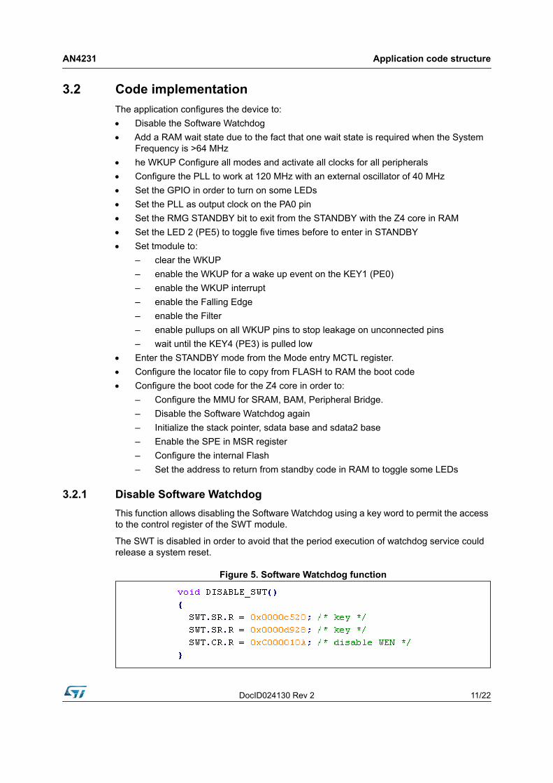
3.2.1 Disable Software WatchdogThis function allows disabling the Software Watchdog using a key word to permit the access to the control register of the SWT module.
The SWT is disabled in order to avoid that the period execution of watchdog service could release a system reset.
Figure 5. Software Watchdog function

Application code structure AN4231
12/22 DocID024130 Rev 2
3.2.2 Clock Generation ModuleThis function allows enabling all modes configuring in the RUNPC[0] mode, all peripheral on and to jump to the PLL configuration function.
Figure 6. CGM init function
3.2.3 PLL configurationThis function allows to select the clock source for the PLL. In this case the PLL is driven by the FXOSC oscillator at 40 MHz.
Then it configures the RUN[0] mode in order to enable the external oscillator, turning on the PLL and setting the PLL as system clock.
The CGM module allows to set the several dividers (Input, loop and output) in order to set the output of the PLL to be at 120 MHz frequency.
Two keys are written in the Mode Entry MCTL register In order to complete the mode entry.
Last part of the function configures the PA0 pin to be a clock out pin where it is possible to measure the PLL frequency divided by four.

DocID024130 Rev 2 13/22
AN4231 Application code structure
Figure 7. PLL configuration function
3.2.4 Reset Generation Module functionThis function allows selecting which core is used for booting after STANDBY exit. If the BOOT_FROM_BKP_RAM is set and if it is boot from FLASH or from backup RAM.
When using the Z4 from RAM in STANDBY mode it needs to ensure that VLE code is used. By default, the Z0 core is the core that is on STANDBY exit.
Figure 8. RGM init function
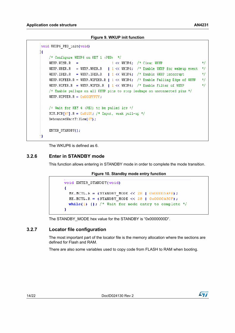
3.2.5 Wakeup Unit configurationThis function allows to enable the Wakeup unit in order to set a wakeup event, enabling the interrupt messaging from the wakeup/interrupt pads to the interrupt controller.
Application code structure AN4231
14/22 DocID024130 Rev 2
Figure 9. WKUP init function
The WKUP6 is defined as 6.
3.2.6 Enter in STANDBY modeThis function allows entering in STANDBY mode in order to complete the mode transition.
Figure 10. Standby mode entry function
The STANDBY_MODE hex value for the STANDBY is “0x0000000D“.
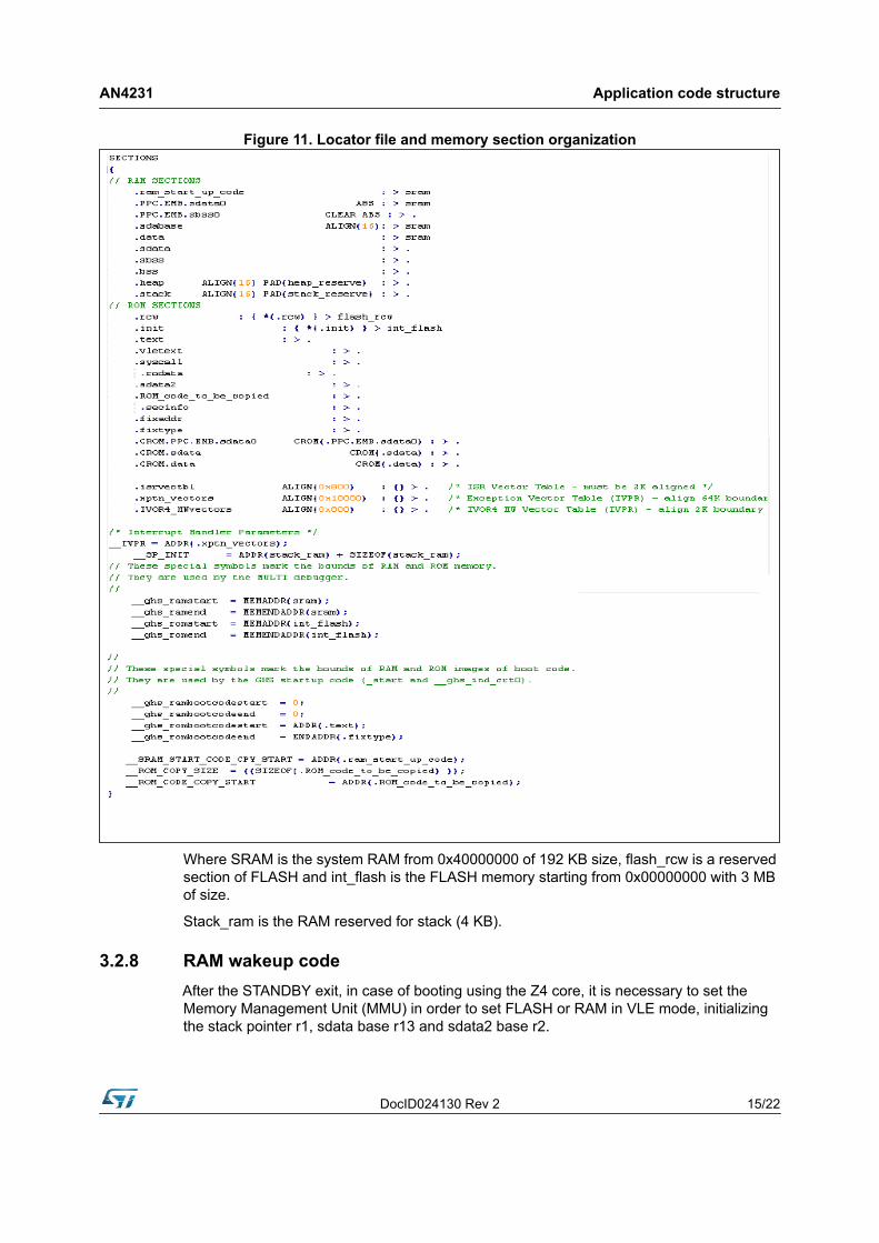
3.2.7 Locator file configurationThe most important part of the locator file is the memory allocation where the sections are defined for Flash and RAM.
There are also some variables used to copy code from FLASH to RAM when booting.
DocID024130 Rev 2 15/22
AN4231 Application code structure
Figure 11. Locator file and memory section organization
Where SRAM is the system RAM from 0x40000000 of 192 KB size, flash_rcw is a reserved section of FLASH and int_flash is the FLASH memory starting from 0x00000000 with 3 MB of size.
Stack_ram is the RAM reserved for stack (4 KB).
3.2.8 RAM wakeup codeAfter the STANDBY exit, in case of booting using the Z4 core, it is necessary to set the Memory Management Unit (MMU) in order to set FLASH or RAM in VLE mode, initializing the stack pointer r1, sdata base r13 and sdata2 base r2.

Application code structure AN4231
16/22 DocID024130 Rev 2
Moreover it is necessary to disable the Software Watchdog and to jump to the code in RAM, to be executed.
All this code is inserted in a section that is copied in the RAM after boot.
RAM Wakeup code function
.section ".ROM_code_to_be_copied", "vax"
.vle
.globl z4_ram_start_code
.align 4
z4_ram_start_code:
#******************
# Enable SPE in MSR
#******************
mfMSR r6
e_or2is r6, 0x0200
mtMSR r6
#TLB4 = pbridgeA
e_lis r3, 0x1004
mtmas0 r3
e_lis r3, 0xC000
e_or2i r3, 0x0800
mtmas1 r3
e_lis r3, 0xC000
e_or2i r3, 0x000A
mtmas2 r3
e_lis r3, 0xC000
e_or2i r3, 0x003F
mtmas3 r3
tlbwe
#TLB6 = Peripheral Bridge and BAM
#0x6 0xC0000600 0xFFC00028 0xFFC0003F
e_lis r3, 0x1006
mtmas0 r3

DocID024130 Rev 2 17/22
AN4231 Application code structure
e_lis r3, 0xC000
e_or2i r3, 0x0600
mtmas1 r3
e_lis r3, 0xFFC0
e_or2i r3, 0x0028
mtmas2 r3
e_lis r3, 0xFFC0
e_or2i r3, 0x003F
mtmas3 r3
tlbwe
#***********************
# re-Configure MMU SRAM - extend from 4K to 256K.
#***********************
e_lis r3, 0x1000
mtmas0 r3
e_lis r3, 0xc000
e_or2i r3, 0x0400 # 256 KB
mtmas1 r3
e_lis r3, 0x4000
e_or2i r3, 0x0028
mtmas2 r3
e_lis r3, 0x4000
e_or2i r3, 0x003f
mtmas3 r3
tlbwe
#disable_watchdog
e_lisr6, 65524
e_add16ir6, r6, -32752
e_lir7, 50464
se_stwr7, 0(r6)
##SWT.SR.R = 0x0000d928; /* key */
e_lisr7, 65524
e_add16ir7, r7, -32752

Application code structure AN4231
18/22 DocID024130 Rev 2
e_lir6, 55592
se_stwr6, 0(r7)
##SWT.CR.R = 0xC000010A; /* disable WEN */
e_lisr6, 65524
e_add16ir6, r6, -32768
e_lisr7, 0xc000
e_add16ir7, r7, 0x010A
se_stwr7, 0(r6)
e_lis r1, __SP_INIT@h # Initialize stack pointer r1 to
e_or2i r1, __SP_INIT@l # value in linker command file.
e_lis r13, _SDA_BASE_@h # Initialize r13 to sdata base
e_or2i r13, _SDA_BASE_@l # (provided by linker).
e_lis r2, _SDA2_BASE_@h # Initialize r2 to sdata2 base
e_or2i r2, _SDA2_BASE_@l # (provided by linker).
e_stwu r0,-64(r1) # Terminate stack.
#TLB2 = 1M Internal flash
e_lis r3, 0x1002
mtmas0 r3
e_lis r3, 0xC000
e_or2i r3, 0x0500
mtmas1 r3
e_lis r3, 0x0000
e_or2i r3, 0x0020
mtmas2 r3
e_lis r3, 0x0000
e_or2i r3, 0x003F
mtmas3 r3
tlbwe
e_lis r3, return_from_standby_code_in_FLASH@h
e_or2i r3, return_from_standby_code_in_FLASH@l
mtlr r3
here: se_blr # branch to code in flash

DocID024130 Rev 2 19/22
AN4231 Application code structure
3.3 ConclusionsSTANDBY mode allows maximizing power saving. During the STANDBY mode, all memories that are not powered down in this mode, enter in a power saving state. This increases the power saving and the data in the memories are retained.
This application note has described how to manage the STANDBY exit from FLASH to RAM, using the Z4 core of the device. This is the lowest power consumption mode and also the fastest for wakeup process because it does not need wait for FLASH initialization.
It is possible (see Figure 8), modifying the RGM init function, to switch from Flash to RAM or from FLASH to FLASH and to decide which core is used. In case of usage of Z0 core at STANDBY exit, no MMU configuration is necessary.

Reference documents AN4231
20/22 DocID024130 Rev 2
Appendix A Reference documents
A.1 Reference documentsSPC564Bxx, SPC56ECxx 32-bit MCU family built on the embedded Power Architecture (Reference manual, RM0070, Doc ID 18196).
DocID024130 Rev 2 21/22
AN4231 Revision history
Revision history
Table 3. Revision history
Date Revision Changes
06-May-2013 1 Initial release.
17-Sep-2013 2 Updated Disclaimer.

AN4231
22/22 DocID024130 Rev 2
Please Read Carefully:
Information in this document is provided solely in connection with ST products. STMicroelectronics NV and its subsidiaries (“ST”) reserve theright to make changes, corrections, modifications or improvements, to this document, and the products and services described herein at anytime, without notice.
All ST products are sold pursuant to ST’s terms and conditions of sale.
Purchasers are solely responsible for the choice, selection and use of the ST products and services described herein, and ST assumes noliability whatsoever relating to the choice, selection or use of the ST products and services described herein.
No license, express or implied, by estoppel or otherwise, to any intellectual property rights is granted under this document. If any part of thisdocument refers to any third party products or services it shall not be deemed a license grant by ST for the use of such third party productsor services, or any intellectual property contained therein or considered as a warranty covering the use in any manner whatsoever of suchthird party products or services or any intellectual property contained therein.
UNLESS OTHERWISE SET FORTH IN ST’S TERMS AND CONDITIONS OF SALE ST DISCLAIMS ANY EXPRESS OR IMPLIED WARRANTY WITH RESPECT TO THE USE AND/OR SALE OF ST PRODUCTS INCLUDING WITHOUT LIMITATION IMPLIED WARRANTIES OF MERCHANTABILITY, FITNESS FOR A PARTICULAR PURPOSE (AND THEIR EQUIVALENTS UNDER THE LAWS OF ANY JURISDICTION), OR INFRINGEMENT OF ANY PATENT, COPYRIGHT OR OTHER INTELLECTUAL PROPERTY RIGHT.
ST PRODUCTS ARE NOT DESIGNED OR AUTHORIZED FOR USE IN: (A) SAFETY CRITICAL APPLICATIONS SUCH AS LIFE SUPPORTING, ACTIVE IMPLANTED DEVICES OR SYSTEMS WITH PRODUCT FUNCTIONAL SAFETY REQUIREMENTS; (B) AERONAUTIC APPLICATIONS; (C) AUTOMOTIVE APPLICATIONS OR ENVIRONMENTS, AND/OR (D) AEROSPACE APPLICATIONS OR ENVIRONMENTS. WHERE ST PRODUCTS ARE NOT DESIGNED FOR SUCH USE, THE PURCHASER SHALL USE PRODUCTS AT PURCHASER’S SOLE RISK, EVEN IF ST HAS BEEN INFORMED IN WRITING OF SUCH USAGE, UNLESS A PRODUCT IS EXPRESSLY DESIGNATED BY ST AS BEING INTENDED FOR “AUTOMOTIVE, AUTOMOTIVE SAFETY OR MEDICAL” INDUSTRY DOMAINS ACCORDING TO ST PRODUCT DESIGN SPECIFICATIONS. PRODUCTS FORMALLY ESCC, QML OR JAN QUALIFIED ARE DEEMED SUITABLE FOR USE IN AEROSPACE BY THE CORRESPONDING GOVERNMENTAL AGENCY.
Resale of ST products with provisions different from the statements and/or technical features set forth in this document shall immediately voidany warranty granted by ST for the ST product or service described herein and shall not create or extend in any manner whatsoever, anyliability of ST.
ST and the ST logo are trademarks or registered trademarks of ST in various countries.Information in this document supersedes and replaces all information previously supplied.
The ST logo is a registered trademark of STMicroelectronics. All other names are the property of their respective owners.
© 2013 STMicroelectronics - All rights reserved
STMicroelectronics group of companies
Australia - Belgium - Brazil - Canada - China - Czech Republic - Finland - France - Germany - Hong Kong - India - Israel - Italy - Japan - Malaysia - Malta - Morocco - Philippines - Singapore - Spain - Sweden - Switzerland - United Kingdom - United States of America
www.st.com