Embed Size (px)
Citation preview

Panasonic Corporation
AN41406A
Product Standards
Page 1 of 22
OverviewAN41406A is a 1-ch motor driver IC. This IC features a low ON resistance and a wide operating supply voltagerange of power supply for motor drive. Adopting an wafer level chip size package (WLCSP) makes it possibleto shrink the mounting area.
Features• 1-ch motor driver IC• Forward reverse drive is possible• It is possible to drive not only a motor but also an actuator• Low ON resistance:
0.19 Ω (upper and lower)• Operating supply voltage range:
Supply voltage range for control 2.7 V to 5.5 V,Supply voltage range for drive 4.0 V to 13.8 V
• Downsizing by adopting an wafer level chip size package• Additional features:
Built-in stand-by function Thermal shutdown circuitLow voltage detection circuit
Applications• DC brush motor, actuator, etc.
Package• 17 pin wafer level chip size package (WLCSP)
Size: 2.41 x 1.91 mmPitch: 0.5 mm
Type• Bi-CDMOS IC
1-ch motor driver IC
Panasonic Corporation
AN41406A
Product Standards
Page 2 of 22
Contents
Overview …………………………………………………………………………………………………………….....1
Features ……………………………………………………………………………………………………………......1
Applications ……………………………………………………………………………………………………..…......1
Package ……………………………………………………………………………………………………………......1
Type ……...………………………………………………………………………………………………………….....1
Application Circuit Example (Block Diagram) ……………………………………………………………….......... 3
Pin Descriptions ……………………………………………………………………………………………………….4
Pin Configuration ………………………………………………………………………………………………………4
Absolute Maximum Ratings …………………………………………………………………………………………. 5
Operating Supply Voltage Range …………………………………………………………………………….......... 5
Allowable Current and Voltage Range ……………………………………………………………………………...6
Electrical Characteristics ……………………………………………………………………………………………7
Electrical Characteristics (Reference values for design) ………………………………………………………...8
Control Pin Mode Table……………………………………………………………………………………………...9
Test Circuit Diagram ………………………………………………………………………………………………..10
Electrical Characteristics Test Procedures ………………………………………………………………………..13
Technical Data………………………………………………………………………………………………………..16
• I/O block circuit diagrams and pin function descriptions ………………………………………………………..16
• Reference data ………………………………………………………………………………………………….....18
Package information ………………………………………………………………………………………….19
Usage Notes ………………………………………………………………………………………………………….20
• Special attention and precaution in using ………………………………………………………………………20
• Notes of Power IC ..…………………………………………………………………………………………………21
• Notes of this IC ……………………………………………………………………………………………………22

Panasonic Corporation
AN41406A
Product Standards
Page 3 of 22
Application Circuit Example (Block Diagram)
Notes:
• This block diagram is for explaining functions. Part of the block diagram may be omitted, or it may be simplified.
• This application circuit is shown as an example but does not guarantee the design for mass production set.
0.01 µF(Strength voltage ≥ VM + 6 V)
VPUMP
5 V47 µF
DMOSH-
bridge
Pre-drive
8 V47 µF
BC1
BC2
VPUMP
VM1
PG1PG2
VM2
FO1
RO1
STBY
VDD
Chargepump
Logic
LowVoltageDetector
Thermalshut down
OSC
GND
ModeSelect
INA
INB
FO2
RO2
PG3A5
B4
B5
B1
A4A3
A1
A2
D3
C3
C2C1
C5C4
D5D4
D1
0.1 µF(Strength voltage ≥ VM + 6 V)
Output ErrorDetection

Panasonic Corporation
AN41406A
Product Standards
Page 4 of 22
Pin Descriptions
Pin No. Pin name Type Description
A1 BC1 Output Charge pump capacitor connection 1
A2 BC2 Output Charge pump capacitor connection 2
A3 VPUMP Output Charge pump output
A4 VDD Power supply Power supply for control circuit
A5 GND Ground Ground for control circuit
B1 STBY Input Total shutdown input
B4 INB Input Inverting input
B5 INA Input Non-inverting input
C1 FO2 Output Non-inverting output 2
C2 FO1 Output Non-inverting output 1
C3 VM2 Power supply Power supply 2 for motor drive
C4 RO2 Output Inverting output 2
C5 RO1 Output Inverting output 1
D1 PG3 Ground Ground 3 for motor drive
D3 VM1 Power supply Power supply 1 for motor drive
D4 PG2 Ground Ground 2 for motor supply
D5 PG1 Ground Ground 1 for motor supply
Pin Configuration (Bottom View)
1
A
2 3 4 5
B
C
D PG3 VM1 PG2 PG1
FO2 VM2 RO2 RO1FO1
BC1
STBY INB INA
BC2 VPUMP VDD GND

Panasonic Corporation
AN41406A
Product Standards
Page 5 of 22
Absolute Maximum Ratings
Operating supply voltage range
ANo.
Parameter Symbol Rating Unit Appropriate Pin No. Notes
1 Supply voltageVDD 6.0
V — *1VM 14.0
2 Supply currentIDD 100
mA — —IM 1 200
3 Power dissipation PD 93 mW — *2
4 Operating ambient temperature Topr –30 to +85 ˚C — *3
5 Storage temperature Tstg –55 to +150 ˚C — *3
6 Drive output current
I(p) DC 1 200(DC) mA
p = C1, C2, C4, C5*4*5
I(p) peak1 6 000(1 ms) mA
I(p) peak2 3 500(10 ms) mA
I(p) peak3 2 000(100 ms) mA
7 Drive output voltage V(m) 14.7 V m = C1, C2, C4, C5 *5
8 Control signal input voltage V(n) GND to VDD V n = B1, B4, B5 —
Notes:
*1 : The values under the condition not exceeding the above absolute maximum ratings and the power dissipation.
The voltage of the charge pump circuit voltage will exceed the supply voltage. The limit voltage of the charge pump is
shown on page 7.
*2 : The power dissipation shown is the value at Ta = 85˚C for the independent (unmounted) IC package without a heat sink.
When using this IC, refer to the PD-Ta diagram of the package standard and design the heat radiation with sufficient margin
so that the allowable value might not be exceeded based on the conditions of power supply voltage, load, and ambient
temperature.
*3 : Except for the power dissipation, operating ambient temperature, and storage temperature, all ratings are for Ta = 25˚C.
*4 : Design the heat radiation with sufficient margin so that the allowable value might not be exceeded based on the time
conditions which the drive output current 6 000 mA is allowed within1 ms and 3 500 mA is allowed within 10 ms and
2 000 mA is allowed within 100 ms. However, the output frequency f requires that f ≤ 5 Hz.
*5 : Do not apply voltage or current from outside to these pin. The setting not exceeding the rating, even transiently, is required.
For the circuit currents, “+” denotes current flowing into the IC, and “–” denotes current flowing out of the IC.
Parameter Symbol Min Typ Max Unit Notes
Supply voltage rangeVDD 2.7 3.3 5.5
V *1VM 4.0 7.4 13.8
Note:
*1: The values under the condition not exceeding the above absolute maximum ratings and the power dissipation.

Panasonic Corporation
AN41406A
Product Standards
Page 6 of 22
Allowable Current and Voltage Range
Notes:
• Allowable current and voltage ranges are limit ranges which do not result in damages to this IC, and IC operation is not
guaranteed within these limit ranges.
• Voltage values, unless otherwise specified, are with respect to GND. GND is voltage for GND, PG1, PG2 and PG3.
GND = PG1 = PG2 = PG3
• VDD is voltage for VDD.
• VM is voltage for VM1 and VM2. VM = VM1 = VM2
• Do not apply external currents or voltages to any pin not specifically mentioned.
• For the circuit currents, "+“ denotes current flowing into the IC, and "-“ denotes current flowing out of the IC.
Pin No. Pin name Rating Unit Notes
A1 BC1 GND to VM V *1
A2 BC2 GND to 19.5 V *1
A3 VPUMP GND to 19 V *1
B1 STBY GND to VDD V —
B4 INB GND to VDD V —
B5 INA GND to VDD V —
C1 FO2 -1.0 to 14.7 V *1
C2 FO1 -1.0 to 14.7 V *1
C4 RO2 -1.0 to 14.7 V *1
C5 RO1 -1.0 to 14.7 V *1
Note:
*1: Do not apply external voltage to this pin. The setting not exceeding the rating, even transiently, is required.

Panasonic Corporation
AN41406A
Product Standards
Page 7 of 22
Electrical Characteristics at VDD = 3.3 V, VM = 7.4 V , STBY = 3.3 VNote: Ta = 25 ˚C 2 ˚C unless otherwise specified.
B No.
Parameter SymbolTest
circuitsConditions
LimitsUnit Notes
Min Typ Max
COMMON BLOCK
Supply Current
1Drive power supply currentin standby mode
IVM 1 STBY = Low — — 800 nA —
2Control power supply currentin standby mode
IDDS 1 STBY = Low — — 800 nA —
3Control power supply currentunder no input
IDDA 1 INA = INB = Low — 1.4 2.0 mA —
Standby Operation
4 STBY high level input voltage VSBH 1 — 2.2 — ― V *1
5 STBY low level input voltage VSBL 1 — — — 0.5 V *1
6 STBY pull-down resistance RSTBY 1 — 100 200 300 kΩ —
Charge Pump Circuit
7 Charge pump voltage VPUMP 1 IPUMP = 0 A 11.4 12.4 13.4 V —
8 Charge pump current capability VPUMPL 1 IPUMP = –500 µA 10.4 11.4 13.4 V —
Driver Block
9 INA, INB high level input voltage VINH 1 — 2.2 — — V *1
10 INA, INB low level input voltage VINL 1 — — — 0.5 V *1
11 INA, INB high level input current IINH 1 INA = INB = 3.3 V 8.3 16.5 33 µA —
12 INA, INB low level input current IINL 1 — –1.0 — — µA —
13Output ON resistance(Upper and Lower)
RON 2 Iout = 500 mA — 0.19 0.24 Ω —
14 Rise time TR 3 — — 0.1 0.2 µs —
15 Fall time TF 3 — — 0.1 0.2 µs —
16 Turn on time TPLH 3 — — 0.4 1.0 µs —
17 Turn off time TPHL 3 — — 0.2 0.5 µs —
Note: *1: Refer to page 9 for the mode setting.
Panasonic Corporation
AN41406A
Product Standards
Page 8 of 22
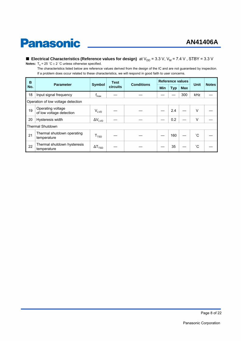
Electrical Characteristics (Reference values for design) at VDD = 3.3 V, VM = 7.4 V , STBY = 3.3 VNotes: Ta = 25 ˚C 2 ˚C unless otherwise specified.
The characteristics listed below are reference values derived from the design of the IC and are not guaranteed by inspection.
If a problem does occur related to these characteristics, we will respond in good faith to user concerns.
B No.
Parameter SymbolTest
circuitsConditions
Reference valuesUnit Notes
Min Typ Max
18 Input signal frequency fmax — — — — 300 kHz —
Operation of low voltage detection
19Operating voltageof low voltage detection
VLVD — — — 2.4 — V —
20 Hysteresis width ∆VLVD — — — 0.2 — V —
Thermal Shutdown
21Thermal shutdown operating temperature
TTSD — — — 160 — ˚C —
22Thermal shutdown hysteresis temperature
∆TTSD — — — 35 — ˚C —

Panasonic Corporation
AN41406A
Product Standards
Page 9 of 22
Control Pin Mode Table
STBY VDD TemperatureInput Logic Output State Charge
PumpCircuit
ModeINA INB FO RO
High
> 2.4 V< 160˚C
High High Low Low
Active
Brake
High Low High Low Normal rotation
Low High Low High Reverse rotation
Low Low
Z * Z *
Mute
≤ 2.4 V
— —
Low voltage detection
> 2.4 V ≥ 160˚C Thermal shutdown
Low — — Mute Standby
Note *: Z means that output is Hi-Z

Panasonic Corporation
AN41406A
Product Standards
Page 10 of 22
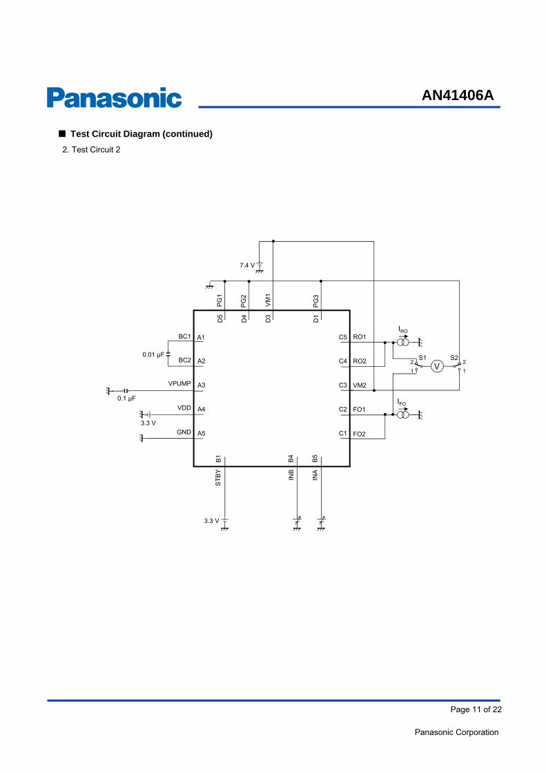
1. Test Circuit 1
Test Circuit Diagram
D1
D3
D4
D5
0.01 µF
B1
B4
B5
A1
A2
A3
A4
A5
C5
C4
C3
C2
C1
INA
INB
ST
BY
RO1
RO2
VM2
FO1
FO2
PG
1
PG
2
VM
1
PG
3
BC2
GND
VDD
VPUMP
BC1
A
A
0.1 µF
3.3 V
7.4 V
V
IPUMP
V
V
A A A
Panasonic Corporation
AN41406A
Product Standards
Page 11 of 22
2. Test Circuit 2
Test Circuit Diagram (continued)
D1
D3
D4
D5
0.01 µF
B1
B4
B5
A1
A2
A3
A4
A5
C5
C4
C3
C2
C1
INA
INB
ST
BY
RO1
RO2
VM2
FO1
FO2
PG
1
PG
2
VM
1
PG
3
BC2
GND
VDD
VPUMP
BC1
0.1 µF
3.3 V
7.4 V
V
IFO
IRO
3.3 V
S12
1
S22
1
Panasonic Corporation
AN41406A
Product Standards
Page 12 of 22
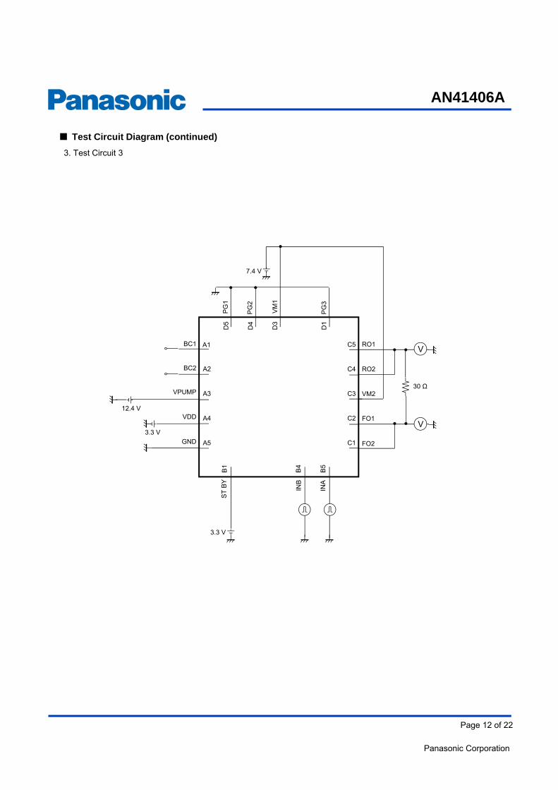
3. Test Circuit 3
Test Circuit Diagram (continued)
D1
D3
D4
D5
B1
B4
B5
A1
A2
A3
A4
A5
C5
C4
C3
C2
C1
INA
INB
ST
BY
RO1
RO2
VM2
FO1
FO2
PG
1
PG
2
VM
1
PG
3
BC2
GND
VDD
VPUMP
BC1
3.3 V
7.4 V
V
V
30 Ω
3.3 V
12.4 V

Panasonic Corporation
AN41406A
Product Standards
Page 13 of 22
Electrical Characteristics Test Procedures
1. Test Circuit 1
CNo.
ParameterInput Output
Pin No. Conditions Pin No. Conditions
COMMON BLOCK
Supply Current
1Drive power supply current in standby mode
B1 STBY = 0 V C3, D3 —
2Control power supply currentin standby mode
B1 STBY = 0 V A4 —
3Control power supply currentunder no input
B1 STBY = 3.3 V A4 —
Standby Operation
4 STBY high level input voltage B1 STBY = variable — Refer to remarks 1.
5 STBY low level input voltage B1 STBY = variable — Refer to remarks 2.
6 STBY pull-down resistance B1 STBY = 3.3V B1 3.3 V / STBY pin current
Charge Pump Circuit
7 Charge pump voltage — IPUMP = 0 mA A3 Output DC voltage
8 Charge pump current capability — IPUMP = –500 µA A3 Output DC voltage
Driver Block
9 INA, INB high level input voltage B4, B5INA = variable,INB = variable
— Refer to remarks 1.
10 INA, INB low level input voltage B4, B5INA = variable, INB = variable
— Refer to remarks 1.
11 INA, INB high level input current B4, B5 INA = INB = 3.3 V B4, B5 INA, INB pin current
12 INA, INB low level input current B4, B5 INA = INB = 0 V B4, B5 INA, INB pin current
Remarks:1: No.4 STBY high level input voltage
No.9 INA, INB high level input voltageNo.10 INA, INB low level input voltage
The conditions of following (1) and (2) must be satisfied when STBY = 2.2 V.(1) Under the conditions that INA = 2.2 V, INB = 0.5 V,
FO1, FO2 pin voltage ≥ 6.4 V AND RO1, RO2 pin voltage ≤ 1 V(2) Under the conditions that INA = 0.5 V, INB = 2.2 V,
RO1, RO2 pin voltage ≥ 6.4 V AND FO1, FO2 pin voltage ≤ 1 V
2: No.5 STBY low level input voltage
Go through change the condition of No.4, STBY = 0.5 V. Each output pin gets into Hi-Z.

Panasonic Corporation
AN41406A
Product Standards
Page 14 of 22
Electrical Characteristics Test Procedures (continued)
2. Test Circuit 2
CNo.
ParameterInput Output
Pin No. Conditions Pin No. Conditions
Driver Block (continued)
13Output ON resistance(Upper and Lower)
C1, C2, C4, C5
IFO = 500 mA,IRO = 500 mA
C1, C2, C4, C5
Refer to remarks 3.
Remarks:3: No.13 Output ON resistance (Upper and Lower)
Operate Setting1, 3 in the following table. Calculate RONU from the differential voltage between FO, RO pin and VM pin.
RONFU = | VM – FO | / | IFO |RONRU = | VM – RO | / | IRO |
In the same way, operate Setting 2, 4 in the following table. Calculate ROND from the differential voltagebetween FO, RO pin and PG pin.
RONFD = | FO – PG | / | IFO |RONRD = | RO – PG | / | IRO |
Due to the above parameters, calculateRON = RONFU + RONRD
RON = RONRU + RONFD
Setting Parameter Symbol INA INB IFO IRO S1 S2
Setting 1 FO Upper-side output ON resistance RONFU 3.3 V 0 V –500 mA — 1 1
Setting 2 FO Lower-side output ON resistance RONFD 0 V 3.3 V +500 mA — 1 2
Setting 3 RO Upper-side output ON resistance RONRU 3.3 V 0 V — –500 mA 2 1
Setting 4 RO Lower-side output ON resistance RONRD 0 V 3.3 V — +500 mA 2 2

Panasonic Corporation
AN41406A
Product Standards
Page 15 of 22
Electrical Characteristics Test Procedures (continued)
3. Test Circuit 3
CNo.
ParameterInput Output
Pin No. Conditions Pin No. Conditions
Driver Block (continued)
14 Rise time B4, B5INA = variable,INB = variable
C1, C2,C4, C5
Load resistance 30 ΩRefer to remarks 4.
15 Fall time B4, B5INA = variable, INB = variable
C1, C2, C4, C5
Load resistance 30 ΩRefer to remarks 4.
16 Turn on time B4, B5INA = variable, INB = variable
C1, C2, C4, C5
Load resistance 30 ΩRefer to remarks 4.
17 Turn off time B4, B5INA = variable, INB = variable
C1, C2, C4, C5
Load resistance 30 ΩRefer to remarks 4.
Remarks:4: No.14 Rise time (TR)
No.15 Fall time (TF)No.16 Turn on time (TPLH)No.17 Turn off time (TPHL)
Measure the periods as shown in the following chart.
TPLH
50%
TPHL
TR TF
50%
80%
20%
INAInput voltage
INBInput voltage
FOOutput voltage
3.3 V
3.3 V
7.4 V
0 V
0 V
0 V
50%
TR TF
50%
80%
20%
ROOutput voltage
7.4 V
0 V
TPLH TPHL

Panasonic Corporation
AN41406A
Product Standards
Page 16 of 22
Technical Data• I/O block circuit diagrams and pin function descriptionsNote: The characteristics listed below are reference values derived from the design of the IC and are not guaranteed.
Pin No.
Waveformand voltage
Internal circuit Impedance Description
A1 — — Charge pump capacitor connection 1
A2 — — Charge pump capacitor connection 2
A3DC
approx. 12.4 V— Charge pump output
A4DC
(Typ. 3.3 V)— Power supply for control circuit VDD
A5,D1,D4,D5
DC0 V
—
A5: Ground for control circuitD1: Ground 3 for motor driveD4: Ground 2 for motor driveD5: Ground 1 for motor drive
B1 — 200 kΩ Total shutdown input
A5
D1
D4
D5
A4
20A1
VM (7.4 V)
25k
A2
5k
10
20A3
25k
5k
VM (7.4 V)
300k
B1
152k
48k
Panasonic Corporation
AN41406A
Product Standards
Page 17 of 22
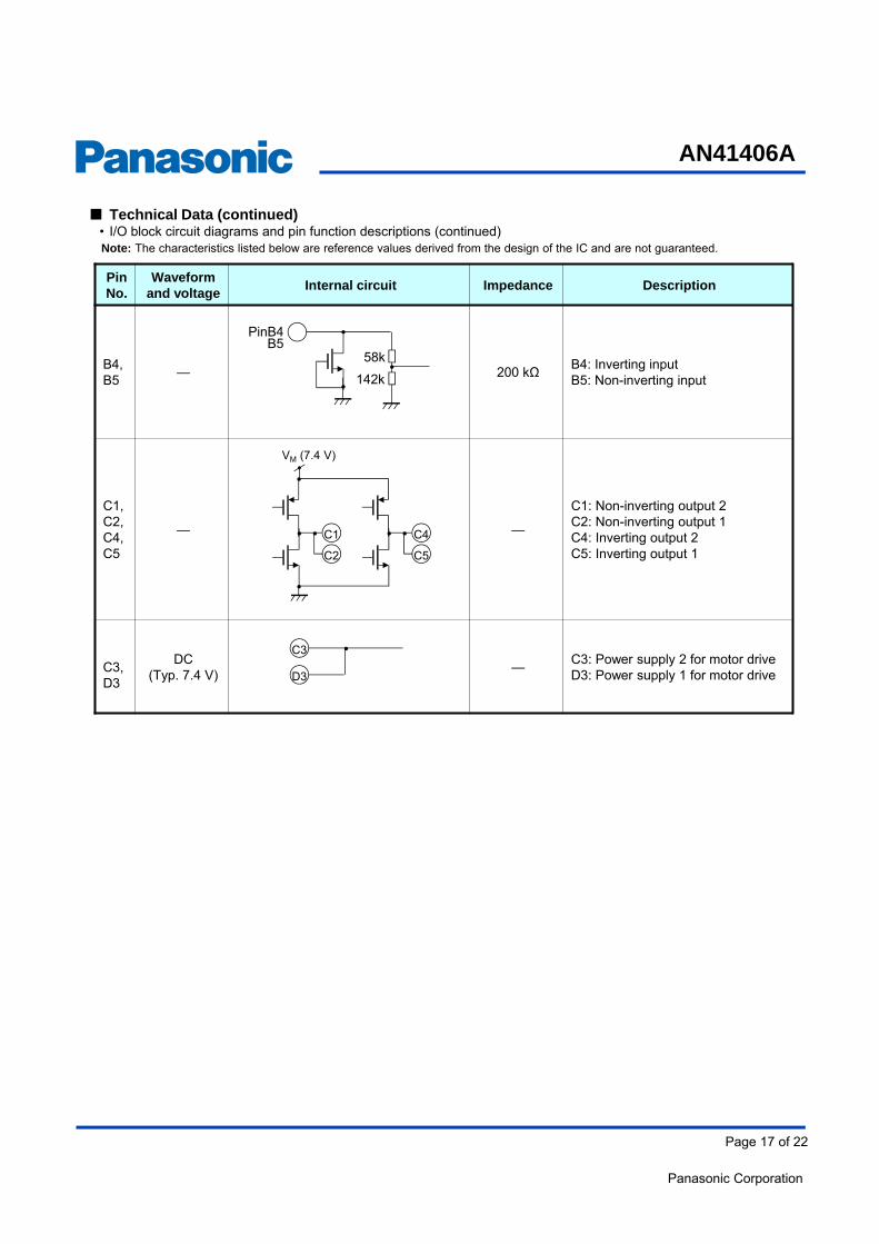
Technical Data (continued)• I/O block circuit diagrams and pin function descriptions (continued)Note: The characteristics listed below are reference values derived from the design of the IC and are not guaranteed.
Pin No.
Waveformand voltage
Internal circuit Impedance Description
B4,B5
— 200 kΩB4: Inverting inputB5: Non-inverting input
C1,C2,C4,C5
— —
C1: Non-inverting output 2C2: Non-inverting output 1C4: Inverting output 2C5: Inverting output 1
C3,D3
DC(Typ. 7.4 V)
—C3: Power supply 2 for motor driveD3: Power supply 1 for motor drive
C3
D3
142k
58k
PinB4B5
C1
VM (7.4 V)
C2
C4
C5

Panasonic Corporation
AN41406A
Product Standards
Page 18 of 22
Technical Data (continued)• Reference dataNote: The characteristics listed below are reference values derived from the design of the IC and are not guaranteed.
Ron changing rate-VDD Characteristics
Ron changing rate-VM Characteristics
–30˚C
25˚C
85˚C
–30˚C
25˚C
85˚C
Ron
cha
ngin
g ra
te[%
]
VDD [V]
40
30
20
10
0
–10
–20
–30
–402.5 3 3.5 4 4.5 5
Ron
cha
ngin
g ra
te[%
]
VM [V]
40
30
20
10
0
–10
–20
–30
50
3.4 4.4 5.4 6.4 7.4

Panasonic Corporation
AN41406A
Product Standards
Page 19 of 22
Package Code : UBGA017-W-2025AELunit : mm
PACKAGE INFORMATION ( Reference Data )
Body Material : Br/Sb Free Epoxy Resin
Reroute Material : Cu
Bump : SnAgCu
Panasonic Corporation
AN41406A
Product Standards
Page 20 of 22
Usage Notes
• Special attention and precaution in using
1. This IC is intended to be used for general electronic equipment [for DC motor for brush, actuator, etc.].Consult our sales staff in advance for information on the following applications:• Special applications in which exceptional quality and reliability are required, or if the failure or malfunction of
this IC may directly jeopardize life or harm the human body.• Any applications other than the standard applications intended.
(1) Space appliance (such as artificial satellite, and rocket)(2) Traffic control equipment (such as for automobile, airplane, train, and ship)(3) Medical equipment for life support(4) Submarine transponder(5) Control equipment for power plant(6) Disaster prevention and security device(7) Weapon(8) Others: Applications of which reliability equivalent to (1) to (7) is required
2. Pay attention to the direction of IC. When mounting it in the wrong direction onto the printed-circuit-board (PCB), it might smoke or ignite.
3. Pay attention in the PCB pattern layout in order to prevent damage due to short circuit between pins. In addition, refer to the Pin Description for the pin configuration.
4. Perform a visual inspection on the PCB before applying power, otherwise damage might happen due to problemssuch as a solder-bridge between the pins of the semiconductor device. Also, perform a full technical verificationon the assembly quality, because the same damage possibly can happen due to conductive substances, such as solder ball, that adhere to the IC during transportation.
5. Take notice in the use of this product that it might break or occasionally smoke when an abnormal state occurssuch as output pin-VCC short (Power supply fault), output pin-GND short (Ground fault), or output-to-output-pinshort (load short) . And, safety measures such as an installation of fuses are recommended because the extent of the above-mentioned damage and smoke emission will depend on the current capability of the power supply.
6. When designing your equipment, comply with the range of absolute maximum rating and the guaranteedoperating conditions (operating power supply voltage and operating environment etc.). Especially, be carefulnot to exceed the range of absolute maximum rating on the transient state, such as power-on, power-off andmode-switching. Otherwise, we will not be liable for any defect which may arise later in your equipment.Even when the products are used within the guaranteed values, take into the consideration of incidence ofbreak down and failure mode, possible to occur to semiconductor products. Measures on the systems such asredundant design, arresting the spread of fire or preventing glitch are recommended in order to prevent physicalinjury, fire, social damages, for example, by using the products.
7. When using the IC for new models, verify the safety including the long-term reliability for each product.8. When the application system is designed by using this IC, be sure to confirm notes in this book.
Be sure to read the notes to descriptions and the usage notes in the book.9. Due to unshielded structure of this IC, under exposure of light, function and characteristic of the product cannot be
guaranteed. During normal operation or even under testing condition, ensure that IC is not exposed to light.10. Basically, chip surface is ground potential. Design to ensure no contact between chip surface and metal shielding.

Panasonic Corporation
AN41406A
Product Standards
Page 21 of 22
Usage Notes (continued)
• Notes of Power IC
1. The protection circuit is for maintaining safety against abnormal operation. Therefore, the protection circuit shouldnot work during normal operation.Especially for the thermal protection circuit, if the area of safe operation (ASO) or the absolute maximum ratingis momentarily exceeded due to output pin to VCC short (Power supply fault), or output pin to GND short
(Ground fault), the IC might be damaged before the thermal protection circuit could operate.
2. Unless specified in the product specifications, make sure that negative voltage or excessive voltage are notapplied to the pins because the device might be damaged, which could happen due to negative voltage orexcessive voltage generated during the ON and OFF timing when the inductive load of a motor coil or actuatorcoils of optical pick-up is being driven.
3. The product which has specified ASO should be operated in ASO.
4. Verify the risks which might be caused by the malfunctions of external components.

Panasonic Corporation
AN41406A
Product Standards
Page 22 of 22
• Notes of this IC
1. Make sure to power on, off, and switching under the standby mode (STBY = Low).
2. Apply voltage from a low-impedance source to VDD and VM. Connect a bypass capacitor to each as near the ICas possible.
3. In case of that the output is changed into Hi-Z (INA = INB = Low) in the rotation of motor, due to the motor currentto flow back into a power source, the supply voltage might rise.
4. If the error detection circuit is active, all outputs are fixed in Hi-Z during the specified time (470 µs 30%). The function is for safety improvements and is not guaranteed nondestructive control.
5. Check the characteristics carefully before using this IC.Preserve sufficient margin in consideration of dispersion of external components and our ICs including not onlystatic characteristics but transition characteristics when using this IC changing external circuit constants.
6. Prohibit mounting with solder dipping and mounting to a flexible cable.
7. The heat thermal resistance is variable due to the mounted status of this IC. To reduce the heat thermalresistance, it is recommended that the power supply and GND pins are connected to a wide metal layer as shortas possible.Refer to the following figure shown an example of a wiring pattern.
Reference value:The heat thermal resistance value (for simulation) in case of the following wiring pattern example
Rth(j-a) = 97˚C / WCondition: Glass-epoxy PWB, 50×50×0.8t (mm), 4-ply
Usage Notes (continued)
Example of a wiring pattern
…Via
…Wiring
1
A
2 3 4 5
B
C
D
FO2 RO2 RO1FO1
STBY INB INA
BC1V
PUMP VDDBC2
PG3 VM1 PG2 PG1
VM2
GND
IC (Top View)

Request for your special attention and precautions in using the technical information andsemiconductors described in this book
(1) If any of the products or technical information described in this book is to be exported or provided to non-residents, the laws and regulations of the exporting country, especially, those with regard to security export control, must be observed.
(2) The technical information described in this book is intended only to show the main characteristics and application circuit examples of the products. No license is granted in and to any intellectual property right or other right owned by Panasonic Corporation or any other company. Therefore, no responsibility is assumed by our company as to the infringement upon any such right owned by any other company which may arise as a result of the use of technical information described in this book.
(3) The products described in this book are intended to be used for general applications (such as office equipment, communications equipment, measuring instruments and household appliances), or for specific applications as expressly stated in this book.Consult our sales staff in advance for information on the following applications: Special applications (such as for airplanes, aerospace, automotive equipment, traffic signaling equipment, combustion equipment,
life support systems and safety devices) in which exceptional quality and reliability are required, or if the failure or malfunction of the products may directly jeopardize life or harm the human body.
It is to be understood that our company shall not be held responsible for any damage incurred as a result of or in connection with your using the products described in this book for any special application, unless our company agrees to your using the products in this book for any special application.
(4) The products and product specifications described in this book are subject to change without notice for modification and/or im-provement. At the final stage of your design, purchasing, or use of the products, therefore, ask for the most up-to-date Product Standards in advance to make sure that the latest specifications satisfy your requirements.
(5) When designing your equipment, comply with the range of absolute maximum rating and the guaranteed operating conditions (operating power supply voltage and operating environment etc.). Especially, please be careful not to exceed the range of absolute maximum rating on the transient state, such as power-on, power-off and mode-switching. Otherwise, we will not be liable for any defect which may arise later in your equipment.
Even when the products are used within the guaranteed values, take into the consideration of incidence of break down and failure mode, possible to occur to semiconductor products. Measures on the systems such as redundant design, arresting the spread of fire or preventing glitch are recommended in order to prevent physical injury, fire, social damages, for example, by using the products.
(6) Comply with the instructions for use in order to prevent breakdown and characteristics change due to external factors (ESD, EOS, thermal stress and mechanical stress) at the time of handling, mounting or at customer's process. When using products for which damp-proof packing is required, satisfy the conditions, such as shelf life and the elapsed time since first opening the packages.
(7) This book may be not reprinted or reproduced whether wholly or partially, without the prior written permission of our company.
20100202


![18V 1ch H-Bridge Motor Driver IC - AKM - Asahi Kasei ... · Junction Temperature 150℃ ... (3mm×3mm) 18V 1ch H-Bridge Motor Driver IC AP1013DEN [AP1013DEN] 014012798-E-00 2014/11](https://img.dokumen.tips/doc/110x75/5b0088977f8b9a952f8d0e1a/18v-1ch-h-bridge-motor-driver-ic-akm-asahi-kasei-temperature-150-.jpg)