Embed Size (px)
Citation preview
Rev C, November 1999
November 2,1999
1
AN4102
C-TV Flyback Type SMPS with SPS
Jeong-Yul Yun
Abstract
Until now, most of the power supply for electronic products were the switching mode power supply.As a product that combined the control IC and the MOSFET, both used in the switching modepower supply, into one package, the SPS attempts to include the maximum number of externalcomponents to reduce the surrounding components as much as possible. It also strengthened itsprotection function. The SPS is available in all SMPS from small power supplies such as thecharger to large power equipments such as adapters, printers, PCs and monitors.
Especially, the SPS (KA3S series) (herein called SPS) described in this note is especially appro-priate for the quasi resonant power supply used mostly in color TVs and is being sold throughrecent production. The SPS is classifed according to the voltage and current rating of the equippedMOSFET. The 5 types in the KA3S series, 800V (6A, 8A) and 650V (7A, 9A, 12A), developed topresent are based on these ratings. Generally, the ßyback or forward method power supply usedmost widely in general electronic products employ the Þxed frequency hard switching method. Formonitors and other TV-like displays, this noise directly affects the display quality. This why thequasi resonant ßyback switching is required.
The quasi resonant-type operation is appropriate for TVs, monitors, VCR-like displays and relatedproducts because it greatly reduces the switching noise from dv/dt by using the snubber capacitoradded between the MOSFET drain and source to extend the switch's turn off time. Furthermore,this method reduces switching loss by turning on the SPS when the voltage across is minimum orzero. The switching frequency of the SPS for TV is determined according the external SYNC circuitthrough SPS #5 pin, S/S (SYNC & SOFT START). According input AC line voltage and load condi-tions, the frequency is made to vary through the SYNC circuit; this minimizes the display noise.
If the voltage of the SPS #5 pin has not reached Vsyth (typ. 6.4V), then, it switches at the internallyset 20kHz frequency. Recently, TV manufacturers are worrying about having to meet the regula-tion on stand-by power consumption (i.e. Energy star in U.S.A.) The SPS executes the Burst Modeoperation in which the SPS switching for a Þxed interval and stops and repeats this type of inter-mittent switching to reduce the switching loss which, in turn, reduces the standby power. ThisBurst Mode opertion can be implemented to satisfy the standby power regulation without having toadd many components.The BURST MODE operation is vital to minimizing the switching loss in thestandby state. To reduce the EMI generated during switching, the SPS is designed with muchlower switching speed than that which drives the general MOSFET. It is designed to have a switch-ing speed which disregards the IC input voltage, V
CC.
2
Rev C, November 1999
In this perspective, not only is the SPS for the TV well-suited for making a low cost, high perfor-mance power supply but also, using few components, to satisfy the standby power consumptionregulation.
1. Important Characteristics
¥ Current Mode Control¥ Quasi-Resonant Operation, Minimum Voltage Switching¥ Low EMI emmision¥ Substitutable for FREE VOLTAGE Power Input¥ Auto Restart after Shutdown¥ Optimum Gate Driver Design¥ Low Standby Power Consumption (BURST MODE OPERATION)¥ Various Protection Circuits¥ Overvoltage protection¥ Overload Protection¥ Thermal shutdown¥ Overcurrent Protection
2. Why the general ßyback method is inappropriate for the TV power supply
In the general ßyback power supply, resonance is mainly generated between the transformer pri-mary inductance and the capacitance, which exists between MOSFET drain-source, after theMOSFET turns off. The instant the MOSFET primary switch turns on, the high voltage charged inthe drain-source capacitor temporarily discharges, generating a large current spike. In the idealcase, the drain-source maximum and minimum voltages are as follows:
Vdsmax = Vdc+(Np/Ns)*Vo
Vdsmin = Vdc-(Np/Ns)*Vo
Np: Number of transformer primary turns
Ns: Number of transformer secondary turns
Vo: Output Voltage
Vdc: Voltage of the rectiÞed AC line (DC link capacitor voltage)
When the MOSFET turns on, a very complex waveform appears and will be affected by the trans-former leakage inductance, MOSFET drain-source capacitance and reverse recovery current ofthe secondary diode etc. If it turns on at a very high voltage, a very large current spike, generatedas the drain-source capacitor discharges, produces noise. The quasi resonance operation exe-cutes minimum or zero voltage switching to reduce this noise.
3
Rev C, November 1999
3. Application Circuit Diagram of TV-use SPS (Figure 17)
The power supply circuit for TV with the KA3S SERIES is composed of the rectiÞer, which rectiÞesthe active power supply line, transformer, start-up circuit, SYNC circuit and feedback circuit. Itssecondary side is the same that of the general ßyback circuit. Unlike the general ßyback and for-ward power supply which uses the RCD snubber circuit the power supply circuit with the KA3Sseries SPS uses the capacitor between the drain and source as the snubber circuit. TVs havemany secondary side output voltages, but 125V used for horizontal deßection and 15V low voltageused as power to sound or other signal processing ICs are the two basic ones. The feedback volt-age (FB) is peak MOSFET drain current. Namely, if the FB voltage increases so does the SPSduty; the secondary side receives more energy which increases the output voltage. When the FBvoltage decreases, the reverse occurs. Two resistors in Figure 15 (VR1+R11, R12) are connectedbetween the output voltage and GND. The resistance of the resistors should be adjusted such thatthe REF pin equals 2.495V (TYP) when the output voltage divide is performed. The results ofactual testing show that about 300k
Ω
resistor between the output voltage and the REF PIN andfew kW resistor between the REF PIN and GND is appropriate for TV.
The capacitor and resistor C10, R8 between the KA431 Q1 cathode and REF pin are selectedbased on the entire system response, but, on the whole, it is best to use a few nf capacitors andfew hundreds kW resistors to make the product of these constants 5-10 times 3k
Ω
* Cfb. As refer-ence, the constants of the 20 inch C-TV demo board circuit are attached at the end of this note.
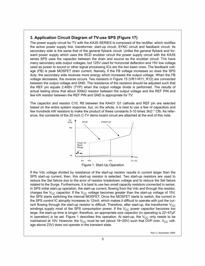
Figure 1. Start-Up Operation
If the Vdc voltage divided by resistance of the start-up resistor results in current larger than theSPS start-up current, then, this start-up resistor is selected. Two start-up resistors are used toreduce the Set failure due to the error of resistor breakdown voltage and to reduce the Set failurerelated to the Surge. Furthermore, it is best to use two small capacity resistors connected in series.In SPS initial start-up operation, the start-up current, ßowing from the Vdc and through the resistor,charges the V
CC
capacitor. If the V
CC
voltage becomes greater than the start-up voltage of 15V,the SPS starts switching the internal MOSFET. Once the MOSFET starts to switch, the current inthe SPS control IC abruptly increases to 12mA, which makes it difÞcult to operate with just the cur-rent ßowing through the start-up resistor is difÞcult. Therefore, after start-up, the transformer V
CC
windings supply most of the SPS consumption power. If the V
CC
power capacitor becomes toolarge, the start-up time is longer; therefore, an appropriate size capacitor (in operating is 22~47µFin operation) is be set. Figure 1 describes this operation. At start-up, the V
CC
only needs to bemaintained at 10V. However, the V
CC
must be set (about 16~20V) such that OVP (min. V
CC
volt-age above 23V) does not operate in the transient state.
Icc[mA]
Iop
Ist
6V 10V 15V Vz [V]
Vcc
STOP START UP
Power OnResetRange

4
Rev C, November 1999
4. Quasi Resonant Circuit Operation
The TV power source circuit has two modes. The Þrst mode is the standby state, and the other isthe normal operation state. When switching starts, the SYNC winding voltage of the V
CC
, similar inshape to the drain-source voltage, charges the SYNC circuit capacitor. As a result, the S/S voltage(#5 pin) greatly increases during ßyback time. When this S/S PIN (#5 pin) voltage exceeds theSYNC reference voltage (6.4V) and the decreases, the SPS starts. By controlling the SYNC circuittime constants, Vds becomes minimum turning on the switch, thus, reduce the current spike andswitching loss.
The snubber capacitor can reduce the snubber voltage spike due to the leakage inductance andthis reduces the EMI.
If the snubber capacitor is too large, the switching loss increases and the standby consumptionpower increases, but, if too small, the increasing switching noise at turn-off becomes a problem.
Though the power supply would be better explained through an equivalent circuit, which consid-ered all the output terminals of the TV power supply, it will be explained assuming having one out-put for it is that way, in principle. Each part of its operation according to time is examined.
Figure 2. Quasi resonant waveform(Vi>Vr)
t5t4t4t3t2t0 t1
VDS1
VGS
VDS
ID
Vcb
VSS
Im
ICR
ID2
Imp
5
Rev C, November 1999
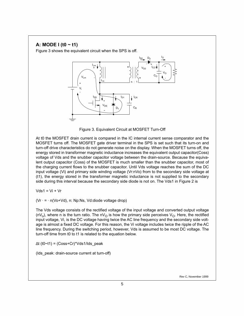
A: MODE I (t0 ~ t1)
Figure 3 shows the equivalent circuit when the SPS is off.
Figure 3. Equivalent Circuit at MOSFET Turn-Off
At t0 the MOSFET drain current is compared in the IC internal current sense comparator and theMOSFET turns off. The MOSFET gate driver terminal in the SPS is set such that its turn-on andturn-off drive characteristics do not generate noise on the display. When the MOSFET turns off, theenergy stored in transformer magnetic inductance increases the equivalent output capacitor(Coss)voltage of Vds and the snubber capacitor voltage between the drain-source. Because the equiva-lent output capacitor (Coss) of the MOSFET is much smaller than the snubber capacitor, most ofthe charging current ßows to the snubber capacitor. Until Vds voltage reaches the sum of the DCinput voltage (Vi) and primary side winding voltage (Vr:nVo) from to the secondary side voltage at(t1), the energy stored in the transformer magnetic inductance is not supplied to the secondaryside during this interval because the secondary side diode is not on. The Vds1 in Figure 2 is
Vds1 = Vi + Vr
(Vr á = á n(Vo+Vd), n: Np:Ns, Vd:diode voltage drop)
The Vds voltage consists of the rectiÞed voltage of the input voltage and converted output voltage(nV
o
), where n is the turn ratio. The nV
O
is how the primary side perceives V
O
. Here, the rectiÞedinput voltage, Vi, is the DC voltage having twice the AC line frequency and the secondary side volt-age is almost a Þxed DC voltage. For this reason, the Vi voltage includes twice the ripple of the ACline frequency. During the switching period, however, Vds is assumed to be most DC voltage. Theturn-off time from t0 to t1 is related to the equation below.
∆
t (t0~t1) = (Coss+Cr)*Vds1/Ids_peak
(Ids_peak: drain-source current at turn-off)
ILm
VLm
Vi
VDSD1
ID1 ICR
CR
+
-
+
-
IDS
Lm
+
ID2IO
CO
D2
VD2
VO
n : 1
ICO
+-+
-
-
6
Rev C, November 1999
B: MODE II (t1 ~ t2)
Figure 4 shows the equivalent circuit when the diode (D
2
) turns on. When Vds voltage reachesVds1 at t1, the equivalent circuit Figure 4 is formed, while the diode connected to the secondaryside transformer winding turns on. The energy stored in the transformer is delivered to the outputterminal electrolytic capacitor (C
O
) and to the load during the time current ßows (until ~t3) due tothe on diode in the secondary side rectiÞer terminal.
The diode current begins to reduce linearly from the ßyback moment but ßows until it becomeszero at a slope proportional to the output voltage and turn ratio (n). During this interval, currentdoes not ßow in the primary side. If this interval time, t1 to t2, is actually calculated, it can beobtained from the equation below.
LMS: Transformer secondary side inductance.
Furthermore, the V
CC
winding deliver energy to the V
CC
capacitor. Lets look at the circuit con-nected to SPS #5 pin the SYNC circuit. This circuit mainly determines when the switch should turnon in the next period. When the drain-source voltage (Vds) becomes minimum, the internal MOS-FET turns on. The V
CC
winding voltage waveform has the Vds voltage waveform and changes to(+) and (-) averaging to zero. The V
CC
winding voltage waveform is determined according to thetransformer turn ratio. As the SYNC circuit connected to #5 half-wave rectiÞes the V
CC
windingvoltage using diode (IN4148), #5 pin voltage increases linearly when the secondary diode turns onand drops when the diode turns off. The moment this voltage passes the IC SYNC circuit thresholdvoltage (Vsync:Typ 6.4V) as it drops, the internal comparator operates to turn the SPS on again.The circuit below shows the charging path when the sync pin voltage increases because of aturned-on diode. In circuit 5, the larger the R3 and C2, the lower the voltage rising slope. The mag-nitude of the Þnal voltage after the increase is determined by the ratio of R2 and equivalent resis-tance of R3//Rss (Rss connected to the internal 5V). The SYNC voltage is limited to 8.4V in the ICinternal circuit. The following equation calculates this voltage.
LmIds_peakn
∆t2------------------------------- VO VD2+=
∆t2LmLmpn
VO VD2+-------------------------=
SYNC H–VcbR3RSS 5R2R3+
R2R3 R3RSS
RSSR+ +--------------------------------------------------------------=

7
Rev C, November 1999
Figure 4. Equivalent Circuit when the Secondary side Diode Turns On
Figure 5. Charging Circuit when the Secondary side Diode Turns On
The resistor and capacitor related to this circuit should be designed carefully such that Sync volt-age does not exceed Vsyth in the standby state but rises to about 8V during normal operation andthat minimum voltage (Vds) switching is veriÞed in normal operation. R1 and R2Õs resistances ofabout few tens k
Ω
~100k
Ω
do not present any problems in testing. A capacitor of lower than aboutfew hundreds pF satisÞes the above conditions.
In this case, the Vds voltage can be divided mainly into two parts. It is the sum of the primary sideinput voltage (Vin) and nV
O
. The applied transformer primary side voltage n (turn ratio) times theoutput voltage (V
O
) when the diode has turned on. Therefore, if there is no leakage inductance,Vds becomes Vin+nV
O
.
ILm
VLm
Vi
VDSD1
ID1 ICR
CR
+
-
+
-
IDS
Lm
+
ID2IO
CO
D2
VD2VO
n : 1
-ICO
++
-
-
YN C HÐ
V cbR 3R SS 5R 2R 3+
R2R 3 R 3R SS R SS R+ +---------------------------------------------------------------=
5
SPS5V
1N4148
D4R2
R3Vcb
50κΩ
C2
Rss
+
−
8
Rev C, November 1999
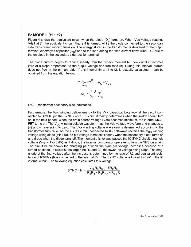
C: MODE III (t2 ~ t4): Resonance Interval
At t2, the diode current becomes zero and turns off because of the applied reverse voltage. Thesecondary side voltage does not affect primary MOSFET voltage any more and, from this point,the charged energy between the output equivalent capacitor (Coss) and the snubber capacitor (Cr)starts to resonate through the primary transformer inductor (Lm). This resonant circuit is composedonly of the DC voltage source (Vin), inductor (Lm) and capacitance (Crs:Coss//Cr). The resonancevoltage and current shape in this case have cosine and sine waveforms, respectively. After passingt3, the inductor voltage polarity reverses, making the current increase. Between passing t3 andreaching t4, the Vlm polarity is + and Vds voltage becomes lower than Vin. As Vlm increases, thecapacitor voltage Vds gradually reduces and its minimum value can be divided into three cases.
Figure 6. Discharging Circuit at Resonance
(1) Vi =Vr(nVo)
In the resonance circuit, the maximum positive (+) inductor voltage (Vlm) is nV
O
(i.e Vr) and Vdsvoltage is Vin minus inductor voltage. In this case, minimum Vds is Vin-nV
O
. Because nV
O
equalsVin, the minimum is zero. The moment Vds voltage reaches the minimum value, the #5 pin voltagecrosses Vsyth through the external SYNC circuit and the SPS internal MOSFET turns on again.Zero voltage switching occurs; MOSFET turn-on loss becomes zero; and noise due to the currentspike at turn-on is not generated.
The resonance interval, Dt3(t2~t4) applicable to half of the LC resonance period is calculated bythe equation above. As shown by the equation above, the resonance interval is proportional to thetransformer inductance and resonance capacitor (Crs), the sum of the MOSFET output capacitorand snubber capacitor. After resonance begins, the V
CC
line voltage stops charging the SYNC cir-cuit capacitor, which starts discharging through the external resistor, R#3 and SPS internal resistor,Rss. Vsync is calculated by the equation below. The SYNC equivalent circuit of this case is shownbelow.
5
SPS5V
50κΩ
C2 R3
Sync
Rss
∆t3 π Lm Crs××=
Crs Coss Cr+=
9
Rev C, November 1999
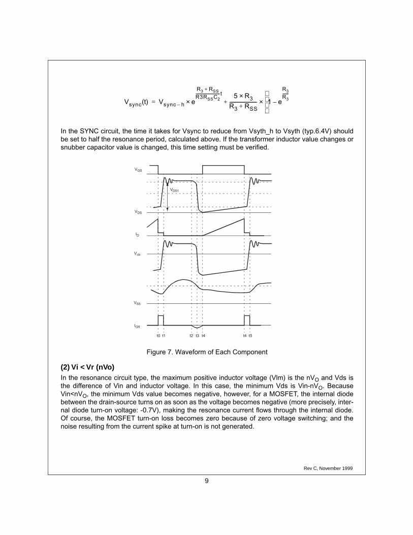
In the SYNC circuit, the time it takes for Vsync to reduce from Vsyth_h to Vsyth (typ.6.4V) shouldbe set to half the resonance period, calculated above. If the transformer inductor value changes orsnubber capacitor value is changed, this time setting must be veriÞed.
Figure 7. Waveform of Each Component
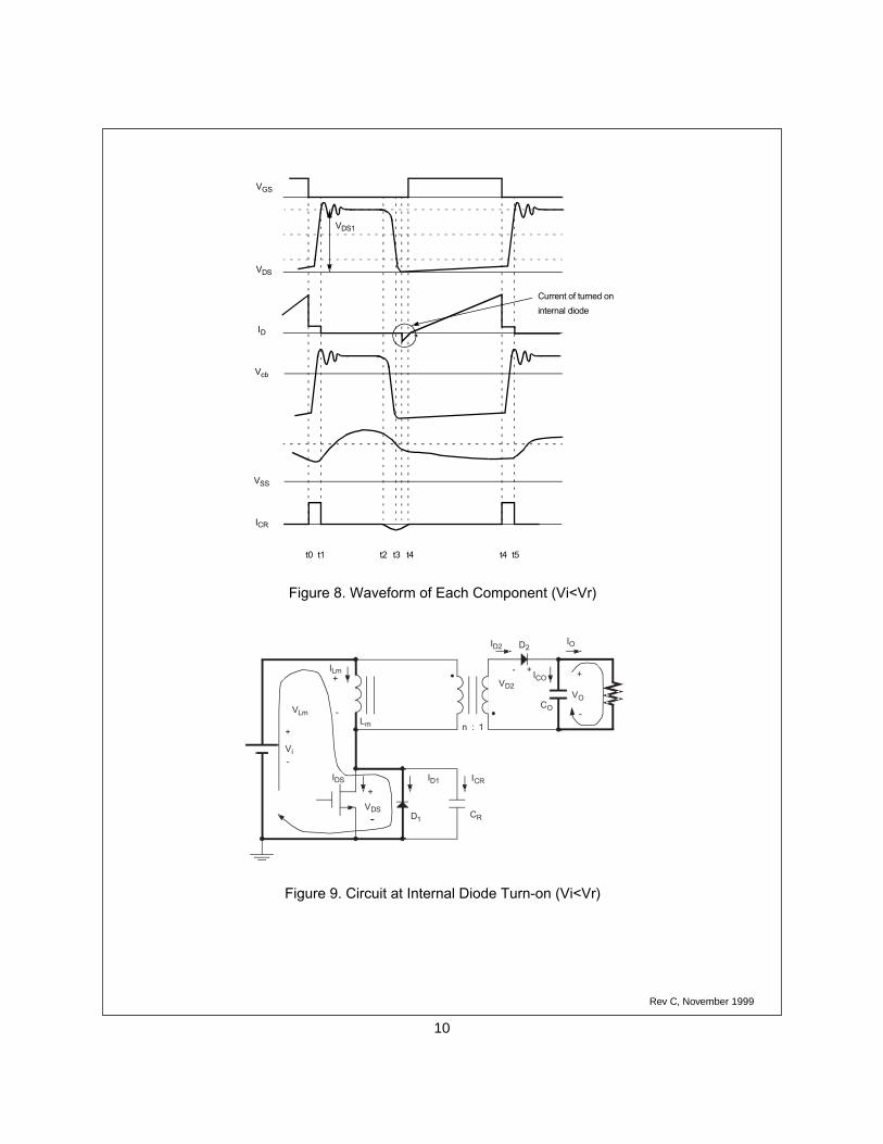
(2) Vi < Vr (nVo)
In the resonance circuit type, the maximum positive inductor voltage (Vlm) is the nV
O and Vds isthe difference of Vin and inductor voltage. In this case, the minimum Vds is Vin-nVO. BecauseVin<nVO, the minimum Vds value becomes negative, however, for a MOSFET, the internal diodebetween the drain-source turns on as soon as the voltage becomes negative (more precisely, inter-nal diode turn-on voltage: -0.7V), making the resonance current ßows through the internal diode.Of course, the MOSFET turn-on loss becomes zero because of zero voltage switching; and thenoise resulting from the current spike at turn-on is not generated.
Vsync(t) Vsync h– e
R3 RSS+
R3RSSC2--------------------------- t 5 R3×
R3 RSS+------------------------ 1 e
R3
R3-------
–
×+×=
t5t4t4t3t2t0 t1
VDS1
VGS
VDS
ID
Vcb
VSS
ICR
10
Rev C, November 1999
Figure 8. Waveform of Each Component (Vi<Vr)
Figure 9. Circuit at Internal Diode Turn-on (Vi<Vr)
t5t4t4t3t2t0 t1
VDS1
VGS
VDS
ID
Vcb
VSS
ICR
Current of turned on
internal diode
ILm
VLm
Vi
VDSD1
ID1 ICR
CR
+
-
+
-
IDS
Lm
+
ID2IO
CO
D2
VD2VO
n : 1
-ICO
+ +
-
-
11
Rev C, November 1999
(3) Vi > Vr(nVo)If Vi becomes greater than nVO, the minimum Vds voltage is Vin-Vr. The charged snubber capaci-tor discharged as SPS turns on.
Vds_min=Vi-Vr (Vr:nVo)
As reviewed in the above three cases, because the MOSFET was made to turn on at either zero orminimum, it generates less noise than the hard switching method. At turn-off, the snubber capaci-tor much larger that the MOSFET output equivalent capacitor (Coss) reduces the Vds rising slope,which reduces the noise generation. If the input voltage is varies, the power supply will operatethrough the above three modes. If the AC line input voltage is low, it will operate through mode (1)or (2) and, if high, through mode (3). Figure 9 shows the circuit with a turned-on internal diodewhen (Vi<Vr).
D: MODE IV (t4 ~ t5): MOSFET Turn-on IntervalIn this interval, the MOSFET turns on and current ßows. The equivalent circuit in this interval isshown above. Input voltage (Vi) is applied to the transformer inductor (Lm) and MOSFET's currentincreases at a linearly. The DC input voltage makes this current's slope equal to (Vi/Lm). Theenergy stored in the transformer internal inductor is proportional to this current. This energy is0.5*Lm* Ipk2 and is supplied to the secondary side when the MOSFET turns off. Because theenergy in the inductor is proportional to the square of the current magnitude, the bigger the outputload, the higher the inductor current. The lower the input voltage and larger the feedback voltage(i.e., the larger the load), the longer the MOSFET turn-on interval, Dt4. The higher the input voltageand lower the output load, the higher the switching frequency becomes.
E. Operation in the STAND BY MODEThe standby mode where the TV is off and it receives only input from the remote control will bereviewed. The output load in the standby mode is very small. In this mode, the MOSFET turn-ontime is very short and, thus, the time required to charge the SYNC circuit voltage is also short andthe input voltage of the SPSÕs SYNC pin cannot reach Vsyth. In this case, it is designed to switchat the SPS internal oscillation frequency (TYP20kHz). Using this method in the standby stategreatly reduces the switching loss but is limited when trying to satisfy the recent consumptionpower regulation of the standby state.
Currently, using a auxiliary-power supply or changing the other secondary circuits has becomecommon in trying to meet this requirement, but these methods have imposed the C-TV manufac-turers because of their additional costs and components. The SPS application satisfying this regu-lation applies the BURST MODE, which will be explained in the last pages of this note. Althoughthe design values are difÞcult to develop as equations through the SPS method, it can be derivedin general form because the parameters of each component have been determined. This methodis a well-suited for meeting the standby state consumption power regulation without adding manycomponents.
A graph of the characteristics of the SPS DEMO BOARD that used 100W input power andKA3S0680R is attached below this page. Then, the BURST MODE operation is explained. Finally,an actual circuit applied with BURST MODE and a PART LIST are attached.
12
Rev C, November 1999
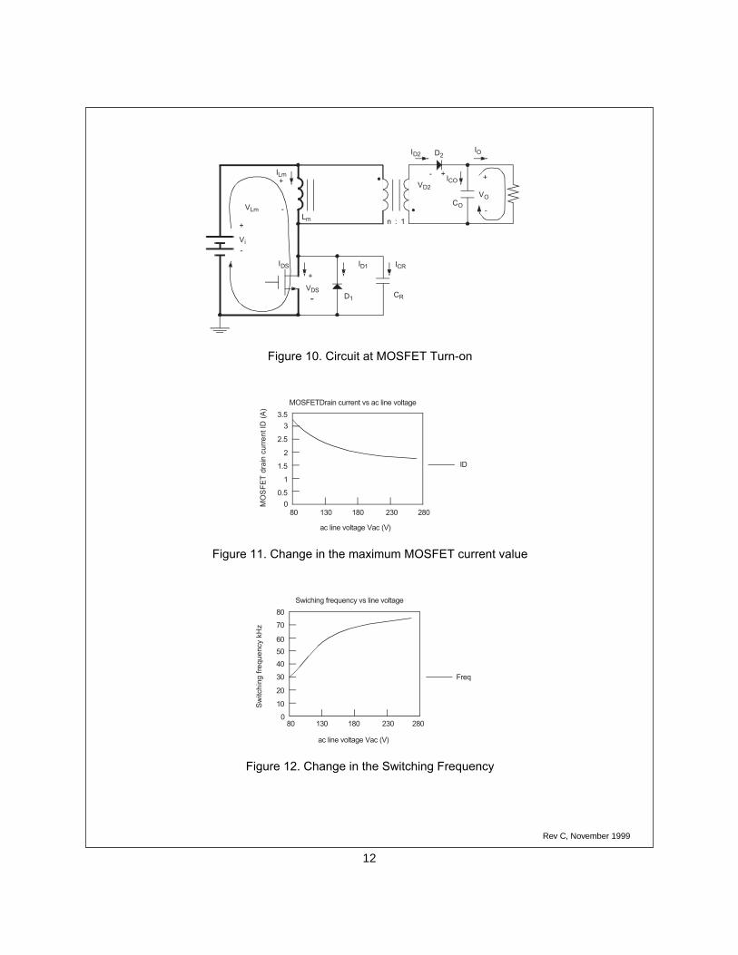
Figure 10. Circuit at MOSFET Turn-on
Figure 11. Change in the maximum MOSFET current value
Figure 12. Change in the Switching Frequency
ILm
VLm
Vi
VDSD1
ID1 ICR
CR
+
-
+
-
IDS
Lm
+
ID2IO
CO
D2
VD2VO
n : 1
-ICO
+ +
-
-
3.5
3
2.5
2
1.5
1
0.5
080 130 180 230 280
MOSFETDrain current vs ac line voltage
MO
SF
ET
dra
in c
urr
en
t ID
(A
)
ac line voltage Vac (V)
ID
80
70
60
50
40
30
20
10
080 130 180 230 280
Swiching frequency vs line voltage
Freq
ac line voltage Vac (V)
Sw
itch
ing
fre
que
ncy
kHz
13
Rev C, November 1999
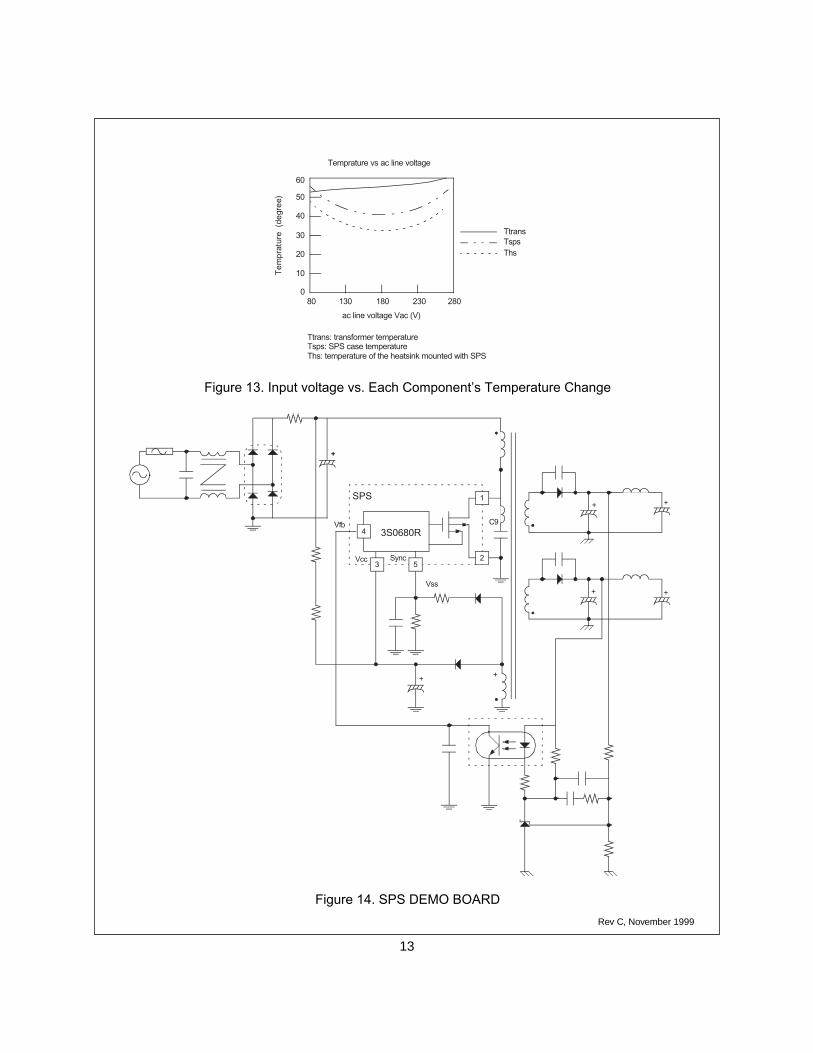
Figure 13. Input voltage vs. Each ComponentÕs Temperature Change
Figure 14. SPS DEMO BOARD
60
50
40
30
20
10
080 130 180 230 280
TtransTspsThs
Temprature vs ac line voltage
Te
mp
ratu
re
(de
gre
e)
ac line voltage Vac (V)
Ttrans: transformer temperatureTsps: SPS case temperatureThs: temperature of the heatsink mounted with SPS
1
2
4
3 5
3S0680R
+
Vfb
Vcc Sync
Vss
C9
+
+
+
+
+
+
SPS
14
Rev C, November 1999
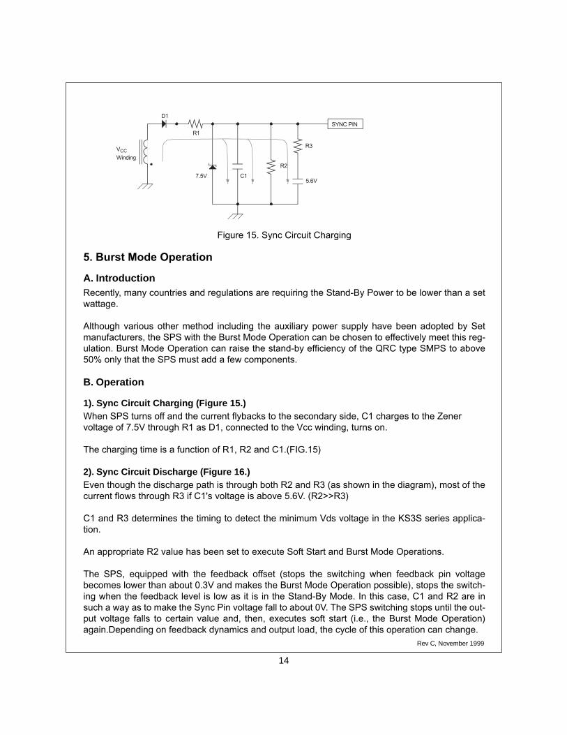
Figure 15. Sync Circuit Charging
5. Burst Mode Operation
A. IntroductionRecently, many countries and regulations are requiring the Stand-By Power to be lower than a setwattage.
Although various other method including the auxiliary power supply have been adopted by Setmanufacturers, the SPS with the Burst Mode Operation can be chosen to effectively meet this reg-ulation. Burst Mode Operation can raise the stand-by efÞciency of the QRC type SMPS to above50% only that the SPS must add a few components.
B. Operation
1). Sync Circuit Charging (Figure 15.)When SPS turns off and the current ßybacks to the secondary side, C1 charges to the Zener voltage of 7.5V through R1 as D1, connected to the Vcc winding, turns on.
The charging time is a function of R1, R2 and C1.(FIG.15)
2). Sync Circuit Discharge (Figure 16.)Even though the discharge path is through both R2 and R3 (as shown in the diagram), most of thecurrent ßows through R3 if C1's voltage is above 5.6V. (R2>>R3)
C1 and R3 determines the timing to detect the minimum Vds voltage in the KS3S series applica-tion.
An appropriate R2 value has been set to execute Soft Start and Burst Mode Operations.
The SPS, equipped with the feedback offset (stops the switching when feedback pin voltagebecomes lower than about 0.3V and makes the Burst Mode Operation possible), stops the switch-ing when the feedback level is low as it is in the Stand-By Mode. In this case, C1 and R2 are insuch a way as to make the Sync Pin voltage fall to about 0V. The SPS switching stops until the out-put voltage falls to certain value and, then, executes soft start (i.e., the Burst Mode Operation)again.Depending on feedback dynamics and output load, the cycle of this operation can change.
R1
7.5V C1
R2
R3
5.6V
SYNC PIN
D1
Winding
VCC

15
Rev C, November 1999
Figure 16. Sync Circuit Discharging
The Sync timing can be truned by appropriately controlling C1 and R2//R3 to eliminate R3 and5.6V Zener, but this requires using within -1% staturated devices, which happen to be inappropri-ate for production.
C. Parameters SettingDevices cannot be set simply through calculations.
Though most are set through testing, the values can be set easily by following the steps, below.
R2 is set experimentally to about 600~800Ω but inversely proportional to the Stand-By Load.
R1 is increased usually to an appropriate value such that the device is int destroyed at output shortor abnormal conditions. However, it is set to match the winding ratio in order to clamp the sync pinvoltage to 7.5V near the end of ßyback.
As C1 becomes larger, the sync timing error, from the deviation of the IC internal sync reference,increases. If C1 becomes smaller, the sync pin voltage becomes less than the feedback pin volt-age in normal operation mode due to the lowering switching frequency from the load increase andall this can cause a shutdown.
An appropriate R3 should be set according to Lm and snubber capacitor to tune the sync timing.
R1
7.5V C1
R2
R3
5.6V
SYNC PIN
16
Rev C, November 1999
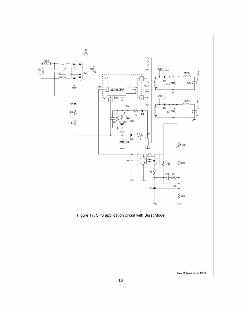
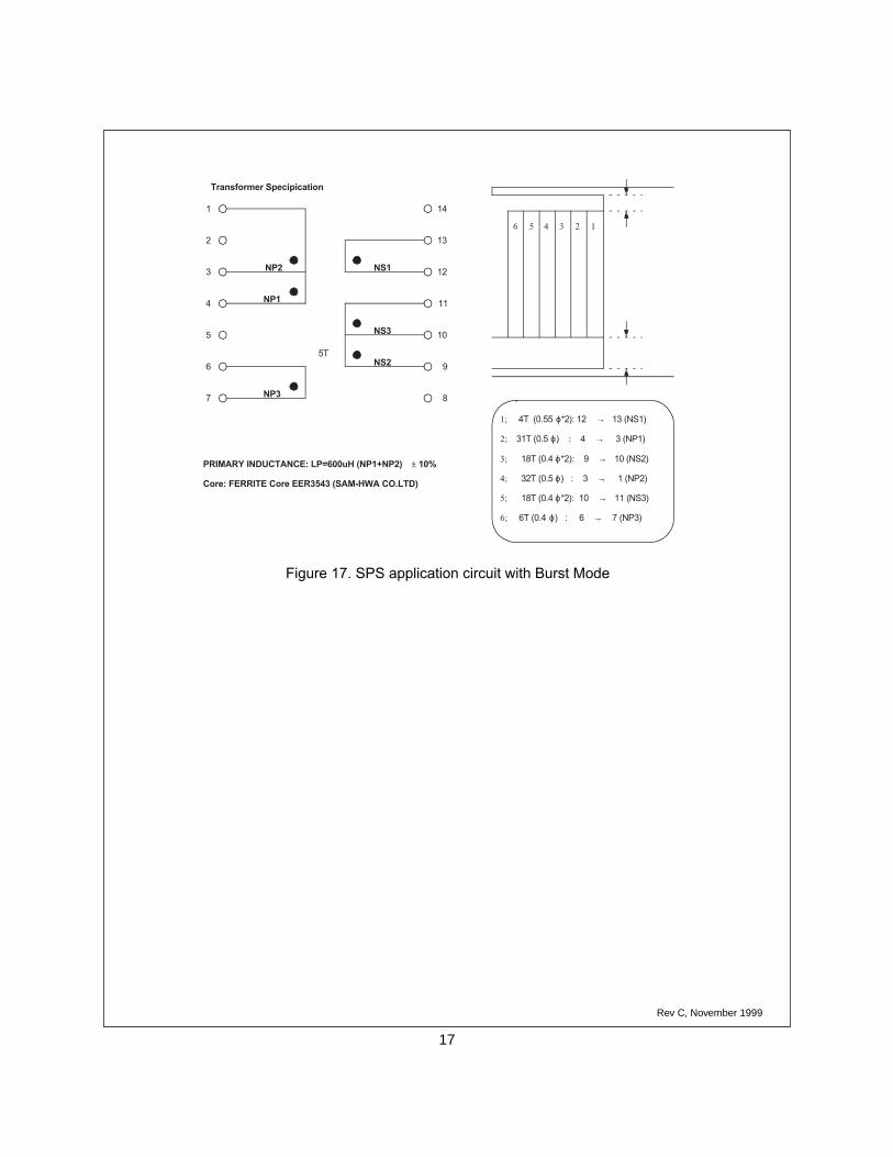
Figure 17. SPS application circuit with Burst Mode
1
2
4
3 5
3S0680RF
+
Vfb
Vcc Sync
Vss
C9
+
+
+
+
+
+
SPS
FUSE
R6
BD C5
D2
R4
R5 C2
R1
R3 ZD2 ZD1
R2 D4
C4
D3 R9
Vx
C3
R7
Q1
OPT1
R10
C10 R8
R11
VR1
R12
C6
C7
D5
C8
C11
Vo
: 1
2VBEAD1
BEAD1
C14
D6C12 C13
Vo
: 1
25
V
17
Rev C, November 1999
Figure 17. SPS application circuit with Burst Mode
1
2
3
4
5
6
7 8
9
10
11
12
13
14
5T
PRIMARY INDUCTANCE: LP=600uH (NP1+NP2) ± 10%
Core: FERRITE Core EER3543 (SAM-HWA CO.LTD)
Transformer Specipication
NP2
NP1
NP3
NS1
NS3
NS2
123
1; 4T (0.55 ϕ*2): 12 → 13 (NS1)
2; 31T (0.5 ϕ) : 4 → 3 (NP1)
3; 18T (0.4 ϕ*2): 9 → 10 (NS2)
4; 32T (0.5 ϕ) : 3 → 1 (NP2)
5; 18T (0.4 ϕ*2): 10 → 11 (NS3)
6; 6T (0.4 ϕ) : 6 → 7 (NP3)
456
18
Rev C, November 1999
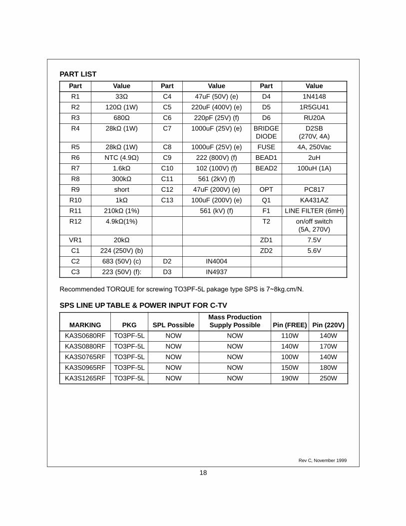
PART LIST
Recommended TORQUE for screwing TO3PF-5L pakage type SPS is 7~8kg.cm/N.
SPS LINE UP TABLE & POWER INPUT FOR C-TV
Part Value Part Value Part Value
R1 33Ω C4 47uF (50V) (e) D4 1N4148
R2 120Ω (1W) C5 220uF (400V) (e) D5 1R5GU41
R3 680Ω C6 220pF (25V) (f) D6 RU20A
R4 28kΩ (1W) C7 1000uF (25V) (e) BRIDGE DIODE
D2SB (270V, 4A)
R5 28kΩ (1W) C8 1000uF (25V) (e) FUSE 4A, 250Vac
R6 NTC (4.9Ω) C9 222 (800V) (f) BEAD1 2uH
R7 1.6kΩ C10 102 (100V) (f) BEAD2 100uH (1A)
R8 300kΩ C11 561 (2kV) (f)
R9 short C12 47uF (200V) (e) OPT PC817
R10 1kΩ C13 100uF (200V) (e) Q1 KA431AZ
R11 210kΩ (1%) 561 (kV) (f) F1 LINE FILTER (6mH)
R12 4.9kΩ(1%) T2 on/off switch (5A, 270V)
VR1 20kΩ ZD1 7.5V
C1 224 (250V) (b) ZD2 5.6V
C2 683 (50V) (c) D2 IN4004
C3 223 (50V) (f): D3 IN4937
MARKING PKG SPL Possible Mass Production Supply Possible Pin (FREE) Pin (220V)
KA3S0680RF TO3PF-5L NOW NOW 110W 140W
KA3S0880RF TO3PF-5L NOW NOW 140W 170W
KA3S0765RF TO3PF-5L NOW NOW 100W 140W
KA3S0965RF TO3PF-5L NOW NOW 150W 180W
KA3S1265RF TO3PF-5L NOW NOW 190W 250W
19
Rev C, November 1999
References[1] Transformer and Inductor Design Handbook, 2Õnd Edition, Colonel Wm. T. McLyman, Marcel
Dekker, Inc., 1988.
[2] ÒFilter Inductor and Flyback Transformer Design for Switching Power SuppliesÓ, Lloyd H.Dixon, Jr., Unitrode Switching Regulated Power Supply Design Seminar Manual, Unitrode Corporation. 1988.
[3] ÒFlyback converter design using SPSÓ, S.T.IM, SPS Application note, Fairchild Electronics
AuthorJeong-Yul Yun is an application engineer in Power Device Division, Fairchild Electronics Co., LTD.
Tel. 82-32-680-1275Fax. 82-32-680-1317E-mail. [email protected]
TRADEMARKS
ACEx™CoolFET™CROSSVOLT™E2CMOSTM
FACT™FACT Quiet Series™FAST®
FASTr™GTO™HiSeC™
The following are registered and unregistered trademarks Fairchild Semiconductor owns or is authorized to use and isnot intended to be an exhaustive list of all such trademarks.
LIFE SUPPORT POLICY
FAIRCHILD’S PRODUCTS ARE NOT AUTHORIZED FOR USE AS CRITICAL COMPONENTS IN LIFE SUPPORTDEVICES OR SYSTEMS WITHOUT THE EXPRESS WRITTEN APPROVAL OF FAIRCHILD SEMICONDUCTOR CORPORATION.As used herein:1. Life support devices or systems are devices orsystems which, (a) are intended for surgical implant intothe body, or (b) support or sustain life, or (c) whosefailure to perform when properly used in accordancewith instructions for use provided in the labeling, can bereasonably expected to result in significant injury to theuser.
2. A critical component is any component of a lifesupport device or system whose failure to perform canbe reasonably expected to cause the failure of the lifesupport device or system, or to affect its safety oreffectiveness.
PRODUCT STATUS DEFINITIONS
Definition of Terms
Datasheet Identification Product Status Definition
Advance Information
Preliminary
No Identification Needed
Obsolete
This datasheet contains the design specifications forproduct development. Specifications may change inany manner without notice.
This datasheet contains preliminary data, andsupplementary data will be published at a later date.Fairchild Semiconductor reserves the right to makechanges at any time without notice in order to improvedesign.
This datasheet contains final specifications. FairchildSemiconductor reserves the right to make changes atany time without notice in order to improve design.
This datasheet contains specifications on a productthat has been discontinued by Fairchild semiconductor.The datasheet is printed for reference information only.
Formative orIn Design
First Production
Full Production
Not In Production
DISCLAIMER
FAIRCHILD SEMICONDUCTOR RESERVES THE RIGHT TO MAKE CHANGES WITHOUT FURTHERNOTICE TO ANY PRODUCTS HEREIN TO IMPROVE RELIABILITY, FUNCTION OR DESIGN. FAIRCHILDDOES NOT ASSUME ANY LIABILITY ARISING OUT OF THE APPLICATION OR USE OF ANY PRODUCTOR CIRCUIT DESCRIBED HEREIN; NEITHER DOES IT CONVEY ANY LICENSE UNDER ITS PATENTRIGHTS, NOR THE RIGHTS OF OTHERS.
TinyLogic™UHC™VCX™
ISOPLANAR™MICROWIRE™POP™PowerTrenchQFET™QS™Quiet Series™SuperSOT™-3SuperSOT™-6SuperSOT™-8