Embed Size (px)
Citation preview

July 2012 Doc ID 022923 Rev 2 1/63
AN4068Application note
ST7580 power line communication system-on-chip design guide
By Riccardo Fiorelli, Mauro Colombo
IntroductionThe ST7580 reference design has been realized as a useful tool that exploits the performance capability of the ST7580 power line networking system-on-chip.
With this reference design, it is possible to evaluate, directly on the power line, the transmitting and receiving performance of a power line communication node based on the ST7580 device.
The line coupling interface is designed to allow the ST7580 device to transmit and receive on the AC mains line using the available FSK and PSK modes within the European CENELEC EN50065-1 standard A band, specified for automatic meter reading (AMR) applications [5]. The circuit has been designed to be easily adapted to different frequency bands and application environments with very few modifications.
An STM32 microcontroller has been included in the reference design to make it more flexible and suitable for use as a standalone smart PLC node.
Figure 1. ST7580 reference design board with outline dimensions
As can be seen from the board image, special effort has been made to make the reference design as compact as possible, while including all the features that enable the ST7580 to perform at its best.
Note: The information provided in this application note refers to the EVALST7580-1 reference design.
www.st.com

Contents AN4068
2/63 Doc ID 022923 Rev 2
Contents
1 Abbreviations used in this document . . . . . . . . . . . . . . . . . . . . . . . . . . . 7
2 Electrical characteristics . . . . . . . . . . . . . . . . . . . . . . . . . . . . . . . . . . . . . 8
3 Safety recommendations . . . . . . . . . . . . . . . . . . . . . . . . . . . . . . . . . . . . 10
4 ST7580 power line networking system-on-chip description . . . . . . . . 11
5 EVALKITST7580-1 evaluation tools . . . . . . . . . . . . . . . . . . . . . . . . . . . . 12
6 Test and measurement tools . . . . . . . . . . . . . . . . . . . . . . . . . . . . . . . . . 13
7 ST7580 reference design description . . . . . . . . . . . . . . . . . . . . . . . . . . 14
7.1 Line coupling section . . . . . . . . . . . . . . . . . . . . . . . . . . . . . . . . . . . . . . . . 20
7.1.1 Transmission active filter . . . . . . . . . . . . . . . . . . . . . . . . . . . . . . . . . . . . 21
7.1.2 Reception passive filter . . . . . . . . . . . . . . . . . . . . . . . . . . . . . . . . . . . . . 23
7.1.3 Power line coupling . . . . . . . . . . . . . . . . . . . . . . . . . . . . . . . . . . . . . . . . 24
7.1.4 Zero crossing coupling . . . . . . . . . . . . . . . . . . . . . . . . . . . . . . . . . . . . . . 27
7.2 STM32 section . . . . . . . . . . . . . . . . . . . . . . . . . . . . . . . . . . . . . . . . . . . . . 29
7.2.1 Direct connections between STM32 microcontroller and ST7580 . . . . . 29
7.2.2 Digital interfaces to the STM32 . . . . . . . . . . . . . . . . . . . . . . . . . . . . . . . 31
7.2.3 General purpose pushbuttons and LEDs . . . . . . . . . . . . . . . . . . . . . . . . 33
8 Reference design standard tests . . . . . . . . . . . . . . . . . . . . . . . . . . . . . . 34
8.1 Input impedance . . . . . . . . . . . . . . . . . . . . . . . . . . . . . . . . . . . . . . . . . . . . 34
8.2 Conducted emission (CE) measurements . . . . . . . . . . . . . . . . . . . . . . . . 35
8.3 EMI immunity tests . . . . . . . . . . . . . . . . . . . . . . . . . . . . . . . . . . . . . . . . . . 40
9 Design guidelines . . . . . . . . . . . . . . . . . . . . . . . . . . . . . . . . . . . . . . . . . . 43
9.1 PCB layout guidelines . . . . . . . . . . . . . . . . . . . . . . . . . . . . . . . . . . . . . . . 43
9.1.1 Thermal performance . . . . . . . . . . . . . . . . . . . . . . . . . . . . . . . . . . . . . . 43
9.1.2 Ground connections . . . . . . . . . . . . . . . . . . . . . . . . . . . . . . . . . . . . . . . . 44
9.2 Thermal impedance and power dissipation calculation . . . . . . . . . . . . . . 44
9.3 Oscillator section . . . . . . . . . . . . . . . . . . . . . . . . . . . . . . . . . . . . . . . . . . . 47

AN4068 Contents
Doc ID 022923 Rev 2 3/63
9.4 Power supply . . . . . . . . . . . . . . . . . . . . . . . . . . . . . . . . . . . . . . . . . . . . . . 47
10 Application ideas . . . . . . . . . . . . . . . . . . . . . . . . . . . . . . . . . . . . . . . . . . . 49
10.1 3-phase architecture . . . . . . . . . . . . . . . . . . . . . . . . . . . . . . . . . . . . . . . . . 49
10.2 Received signal strength indication (RSSI) . . . . . . . . . . . . . . . . . . . . . . . 52
11 FAQs and troubleshooting . . . . . . . . . . . . . . . . . . . . . . . . . . . . . . . . . . . 53
11.1 FAQs . . . . . . . . . . . . . . . . . . . . . . . . . . . . . . . . . . . . . . . . . . . . . . . . . . . . 53
11.2 Troubleshooting . . . . . . . . . . . . . . . . . . . . . . . . . . . . . . . . . . . . . . . . . . . . 55
12 References . . . . . . . . . . . . . . . . . . . . . . . . . . . . . . . . . . . . . . . . . . . . . . . . 57
13 Normative references . . . . . . . . . . . . . . . . . . . . . . . . . . . . . . . . . . . . . . . 58
Appendix A Board layout . . . . . . . . . . . . . . . . . . . . . . . . . . . . . . . . . . . . . . . . . . . . 59
Revision history . . . . . . . . . . . . . . . . . . . . . . . . . . . . . . . . . . . . . . . . . . . . . . . . . . . . 62

List of tables AN4068
4/63 Doc ID 022923 Rev 2
List of tables
Table 1. Electrical and thermal characteristics of the ST7580 reference design . . . . . . . . . . . . . . . . 8Table 2. TX_OUT level vs. TX_GAIN - typical values. . . . . . . . . . . . . . . . . . . . . . . . . . . . . . . . . . . . . 9Table 3. Bill of material . . . . . . . . . . . . . . . . . . . . . . . . . . . . . . . . . . . . . . . . . . . . . . . . . . . . . . . . . . . 17Table 4. Line coupling transformer specifications. . . . . . . . . . . . . . . . . . . . . . . . . . . . . . . . . . . . . . . 25Table 5. Zero crossing coupling - measured timing characteristics . . . . . . . . . . . . . . . . . . . . . . . . . 28Table 6. Connections between STM32F103CBT6 and ST7580 devices on EVALST80-1 board . . 30Table 7. Document revision history . . . . . . . . . . . . . . . . . . . . . . . . . . . . . . . . . . . . . . . . . . . . . . . . . 62

AN4068 List of figures
Doc ID 022923 Rev 2 5/63
List of figures
Figure 1. ST7580 reference design board with outline dimensions . . . . . . . . . . . . . . . . . . . . . . . . . . . 1Figure 2. ST7580 block diagram . . . . . . . . . . . . . . . . . . . . . . . . . . . . . . . . . . . . . . . . . . . . . . . . . . . . 11Figure 3. Board drawing with the various sections indicated . . . . . . . . . . . . . . . . . . . . . . . . . . . . . . . 14Figure 4. Schematics of the ST7580 reference design board (part 1) . . . . . . . . . . . . . . . . . . . . . . . . 15Figure 5. Schematics of the ST7580 reference design board (part 2) . . . . . . . . . . . . . . . . . . . . . . . . 16Figure 6. Line coupling section schematics . . . . . . . . . . . . . . . . . . . . . . . . . . . . . . . . . . . . . . . . . . . . 20Figure 7. Measured frequency response of the transmission active filter (typical) . . . . . . . . . . . . . . 22Figure 8. Montecarlo simulation of the transmission active filter frequency response. . . . . . . . . . . . 22Figure 9. Measured frequency response of the reception passive filter (typical) . . . . . . . . . . . . . . . . 24Figure 10. Montecarlo simulation of the reception passive filter response . . . . . . . . . . . . . . . . . . . . . 24Figure 11. Measured frequency response of the transmission line coupling loaded with the EN50065-1 LISN impedance (typical)26Figure 12. Measured frequency response of the transmission line coupling loaded with 5 W + 15 µF
(typical) . . . . . . . . . . . . . . . . . . . . . . . . . . . . . . . . . . . . . . . . . . . . . . . . . . . . . . . . . . . . . . . . 26Figure 13. Montecarlo simulation of the transmission line coupling response loaded with the
EN50065-1 LISN impedance . . . . . . . . . . . . . . . . . . . . . . . . . . . . . . . . . . . . . . . . . . . . . . . 27Figure 14. Isolated zero crossing coupling circuit . . . . . . . . . . . . . . . . . . . . . . . . . . . . . . . . . . . . . . . . 27Figure 15. Zero crossing coupling - positive edge delay . . . . . . . . . . . . . . . . . . . . . . . . . . . . . . . . . . . 28Figure 16. Zero crossing coupling - negative edge delay . . . . . . . . . . . . . . . . . . . . . . . . . . . . . . . . . . 28Figure 17. Connections between the STM32F103CBT6 and the ST7580 devices on the
EVALST80-1 board. . . . . . . . . . . . . . . . . . . . . . . . . . . . . . . . . . . . . . . . . . . . . . . . . . . . . . . 30Figure 18. STM32F103CB external connections: schematics . . . . . . . . . . . . . . . . . . . . . . . . . . . . . . . 32Figure 19. STM32 configurable signalling LEDs and pushbuttons . . . . . . . . . . . . . . . . . . . . . . . . . . . 33Figure 20. Measured input impedance modulus of the line coupling - reception mode (typical) . . . . . 35Figure 21. Measured input impedance modulus of the line coupling - transmission mode (typical) . . 35Figure 22. Conducted emissions test setup. . . . . . . . . . . . . . . . . . . . . . . . . . . . . . . . . . . . . . . . . . . . . 36Figure 23. Conducted emissions: PSK transmission spectrum, peak measurement, 9 kHz - 150 kHz,
line-to-earth. . . . . . . . . . . . . . . . . . . . . . . . . . . . . . . . . . . . . . . . . . . . . . . . . . . . . . . . . . . . . 37Figure 24. Conducted emissions: PSK transmission spectrum, peak measurement, 9 kHz - 150 kHz,
neutral-to-earth . . . . . . . . . . . . . . . . . . . . . . . . . . . . . . . . . . . . . . . . . . . . . . . . . . . . . . . . . . 37Figure 25. Conducted emissions: PSK transmission spectrum, quasi-peak measurement, 150 kHz -
30 MHz, line-to-earth . . . . . . . . . . . . . . . . . . . . . . . . . . . . . . . . . . . . . . . . . . . . . . . . . . . . . 38Figure 26. Conducted emissions: PSK transmission spectrum, quasi-peak measurement, 150 kHz -
30 MHz, neutral-to-earth . . . . . . . . . . . . . . . . . . . . . . . . . . . . . . . . . . . . . . . . . . . . . . . . . . . 38Figure 27. Conducted emissions: FSK transmission spectrum, peak measurement, 9 kHz - 150 kHz
, line-to-earth. . . . . . . . . . . . . . . . . . . . . . . . . . . . . . . . . . . . . . . . . . . . . . . . . . . . . . . . . . . . 39Figure 28. Conducted emissions: FSK transmission spectrum, peak measurement, 9 kHz - 150 kHz,
neutral-to-earth . . . . . . . . . . . . . . . . . . . . . . . . . . . . . . . . . . . . . . . . . . . . . . . . . . . . . . . . . . 39Figure 29. Conducted emissions: FSK transmission spectrum, quasi-peak measurement, 150 kHz -
30 MHz, line-to-earth . . . . . . . . . . . . . . . . . . . . . . . . . . . . . . . . . . . . . . . . . . . . . . . . . . . . . 40Figure 30. Conducted emissions: FSK transmission spectrum, quasi-peak measurement, 150 kHz -
30 MHz, neutral-to-earth . . . . . . . . . . . . . . . . . . . . . . . . . . . . . . . . . . . . . . . . . . . . . . . . . . . 40Figure 31. Common mode disturbance protection - positive disturbance . . . . . . . . . . . . . . . . . . . . . . 41Figure 32. Common mode disturbance protection - negative disturbance. . . . . . . . . . . . . . . . . . . . . . 42Figure 33. Differential mode disturbance protection . . . . . . . . . . . . . . . . . . . . . . . . . . . . . . . . . . . . . . 42Figure 34. Example of stencil openings for the QFN48 package. . . . . . . . . . . . . . . . . . . . . . . . . . . . . 43Figure 35. PCB copper dissipating area on top layer (left) and bottom layer (right) for the ST7580
reference design board. . . . . . . . . . . . . . . . . . . . . . . . . . . . . . . . . . . . . . . . . . . . . . . . . . . . 44

List of figures AN4068
6/63 Doc ID 022923 Rev 2
Figure 36. Packet-fragmented transmission . . . . . . . . . . . . . . . . . . . . . . . . . . . . . . . . . . . . . . . . . . . . 45Figure 37. Measured ST7580 thermal impedance curve (typical) . . . . . . . . . . . . . . . . . . . . . . . . . . . . 45Figure 38. Simulation model of the thermal impedance ZthJA of the ST7580 mounted on the
reference design board. . . . . . . . . . . . . . . . . . . . . . . . . . . . . . . . . . . . . . . . . . . . . . . . . . . . 46Figure 39. Example of power supply EMI input filter . . . . . . . . . . . . . . . . . . . . . . . . . . . . . . . . . . . . . . 48Figure 40. Scheme of principle for non-switched 3-phase architecture . . . . . . . . . . . . . . . . . . . . . . . . 49Figure 41. Scheme of principle for switched 3-phase architecture . . . . . . . . . . . . . . . . . . . . . . . . . . . 50Figure 42. 3-phase isolated zero crossing coupling circuit . . . . . . . . . . . . . . . . . . . . . . . . . . . . . . . . . 51Figure 43. 3-phase non-isolated zero crossing coupling circuit . . . . . . . . . . . . . . . . . . . . . . . . . . . . . . 52Figure 44. PCB layout - components . . . . . . . . . . . . . . . . . . . . . . . . . . . . . . . . . . . . . . . . . . . . . . . . . . 59Figure 45. PCB layout - top view . . . . . . . . . . . . . . . . . . . . . . . . . . . . . . . . . . . . . . . . . . . . . . . . . . . . . 60Figure 46. PCB layout - bottom view . . . . . . . . . . . . . . . . . . . . . . . . . . . . . . . . . . . . . . . . . . . . . . . . . . 61

AN4068 Abbreviations used in this document
Doc ID 022923 Rev 2 7/63
1 Abbreviations used in this document
● AC = alternate current
● AFE = analog front end
● AMR = automated meter reading
● AWGN = additive white gaussian noise
● BER = bit error rate
● BOM = bill of material
● CE = conducted emissions
● DC = direct current
● DL = data link layer
● DSP = digital signal processor
● EMC = electro-magnetic compliance
● EMI = electro-magnetic interference
● FSK = frequency shift keying
● GUI = graphical user interface
● NBI = narrow-band interferer
● LISN = line impedance stabilization network
● PA = power amplifier
● PCB = printed circuit board
● PHY = physical layer
● PLC = power line communication
● PSK = phase shift keying
● PSU = power supply unit
● RBW = resolution bandwidth
● SBW = signal bandwidth
● SNR = signal-to-noise ratio
● SoC = system-on-chip.
Electrical characteristics AN4068
8/63 Doc ID 022923 Rev 2
2 Electrical characteristics
Table 1. Electrical and thermal characteristics of the ST7580 reference design
ParameterValue
NotesMin. Typ. Max. Unit
Thermal data
Ambient operating temperature -40 85 °C
ST7580 thermal resistance 50 (1) °C/WMeasured on the ST7580 reference design
2-side PCB with thermal pad and 4x4 thermal via array
Transceiver section
Transmitting specifications (Tx mode)
Transmitted signal -20 dB bandwidth
20 kHz FSK 9600 baud
14.5 Any PSK mode
Transmitted output current limit 1 A rms
Receiving specifications (Rx mode)
Minimum detectable received signal
44dBµ
VrmsB-PSK coded,
fC = 86 kHz, BER = 10-3
58B-FSK, 9600 baud, fC = 86 kHz,
deviation=1, BER=10-3
Reception filter -3 dB bandwidth 65 kHz
Mains coupling specifications
Transformer isolation 4 (2) kV
Power supply requirements
VCC power supply voltage 8 13 18 V
VCC power supply current absorption – RX mode
5 mAJP7 closed (LK112SM33TR LDO not
enabled)
65 mA JP7 open (LK112SM33TR LDO enabled)
VCC power supply current absorption – TX mode
20 500 mAVCC = 8 to 18 V,
I(PA_OUT) = 0 to 1 A rms
VDDIO digital supply voltage -10% 3.3 +10% V
VDDIO digital supply current absorption
60 mAJP7 closed
No digital connection to external equipment
1. Measured over a continuous transmission period of 3000 seconds (steady-state thermal dissipation). See Figure 39 for thermal impedance typical curve.
2. Note that ST does not guarantee transformer isolation. ST assumes no responsibility for the consequences that may arise from such risks.

AN4068 Electrical characteristics
Doc ID 022923 Rev 2 9/63
Table 2. TX_OUT level vs. TX_GAIN - typical values
TX_GAIN
TX_OUT
[V p-p][dBµV rms]
FSK PSK
31 3.900 123 120
30 3.450 122 119
29 3.100 121 118
28 2.750 120 117
27 2.450 119 116
26 2.200 118 115
25 1.950 117 114
24 1.750 116 113
23 1.550 115 112
22 1.380 114 111
21 1.225 113 110
20 1.100 112 109
19 0.975 111 108
18 0.870 110 107
17 0.775 109 106
16 0.690 108 105
15 0.615 107 104
14 0.550 106 103
13 0.490 105 102
12 0.435 104 101
11 0.390 103 100
10 0.345 102 99
9 0.310 101 98
8 0.275 100 97
7 0.245 99 96
6 0.220 98 95
5 0.195 97 94
4 0.175 96 93
3 0.155 95 92
2 0.140 94 91
1 0.125 93 90
0 0.110 92 89

Safety recommendations AN4068
10/63 Doc ID 022923 Rev 2
3 Safety recommendations
The board must be used by expert technicians only. Due to the high voltage (85-265 Vac) present on the non-isolated parts, special care must be taken in order to avoid the risk of electric shock.
There is no protection against accidental contact with high-voltages.
After disconnection of the board from the mains, no live parts must be touched immediately because of the energized capacitors.
It is mandatory to use a mains insulation transformer to perform any tests on the high-voltage sections, using test instruments such as, for instance, spectrum analyzers or oscilloscopes.
Do not connect any probe to the high-voltage sections if the board is not isolated from the mains supply, in order to avoid damage to instruments and demo tools.
ST assumes no responsibility for the consequences of any improper use of this development tool.

AN4068 ST7580 power line networking system-on-chip description
Doc ID 022923 Rev 2 11/63
4 ST7580 power line networking system-on-chip description
The ST7580 is a flexible power line networking system-on-chip (SOC) combining a high performing PHY DSP core and a protocol controller core with a fully integrated analog front-end (AFE) and line driver for a scalable future-proof, cost effective single-chip narrow-band power line communication solution.
The device comes with embedded firmware providing a complete physical layer (PHY) and some data link layer (DL) services for power line communication. The ST7580 protocol services have been developed mainly for smart metering applications using CENELEC A band, but they are also suitable for other command and control applications.
The embedded PHY layer, hosted in a DSP engine, implements two different modulation schemes: a B-FSK modulation up to 9.6 kbps and a multi-mode PSK modulation with channel quality estimation, dual channel receiving mode and convolutional coding, delivering a throughput up to 28.8 kbps.
The embedded DL layer hosted in the embedded microcontroller offers framing and error correction services.
Communication with an external microcontroller is based on a UART host interface, exporting all the functions and services required to configure and control the device and its protocol stack.
For further details, please refer to [1] and [2].
Figure 2. ST7580 block diagram

EVALKITST7580-1 evaluation tools AN4068
12/63 Doc ID 022923 Rev 2
5 EVALKITST7580-1 evaluation tools
The minimum set of evaluation tools to test the ST7580 power line communication requires two communication nodes, each made up of the following elements:
● a PC running the ST7580 GUI software tool
● one EVALKITST7580-1 demonstration kit, composed of two boards:
– EVALST7580-1 PLC board;
– one EVLALTAIR900-M1 board as power supply unit (PSU).
For further details regarding the ST7580 GUI software and the available evaluation tools, please visit http://www.st.com/powerline.

AN4068 Test and measurement tools
Doc ID 022923 Rev 2 13/63
6 Test and measurement tools
● Spectrum / network / impedance analyzer
– Agilent 4395A: 10 Hz - 500 MHz
● Agilent 43961A impedance test kit
– Differential active probe
● Agilent 1141A differential probe: 1 MΩ, 7 pF
● Agilent 1142A probe control and power module: DC reject 0.05 Hz
● EMC analyzer
– Rohde&Schwarz ESL
– 9 kHz - 3 GHz
● Two-line V-network (LISN)
– Rohde&Schwarz ENV216
● Isolation transformer
– 1000 VA, 0 - 250 V variable output
● Oscilloscope
– Tektronix DPO 7104C: 1 GHz, 20 GS/s
● Surge/burst generator
– Volta UCS 500-M.

ST7580 reference design description AN4068
14/63 Doc ID 022923 Rev 2
7 ST7580 reference design description
The ST7580 reference design is made up of the following sections:
● ST7580 device section
● Line coupling section, including four subsections:
– Transmission active filter
– Reception passive filter
– Power line coupling
– Zero crossing coupling
● STM32 microcontroller section.
The board has also six external connections:
– AC mains (line and neutral) on CN1 connector;
– VCC (8 to 18 V) and VDDIO (3.3 or 5 V) supply voltages on CN2 connector
– SD storage card on CN3 micro SD connector
– USB interface for PC connectivity on CN4 mini-USB connector
– Digital interface on J2 (5x2 connector), collecting UART and I2C digital access to the onboard STM32 microcontroller
– JTAG interface for STM32 microcontroller on JTAG1 connector (10x2 connector).
Figure 3. Board drawing with the various sections indicated
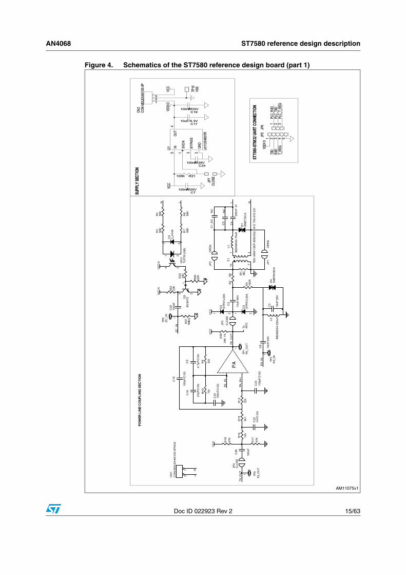
Figure 4 gives a global view of the reference design.
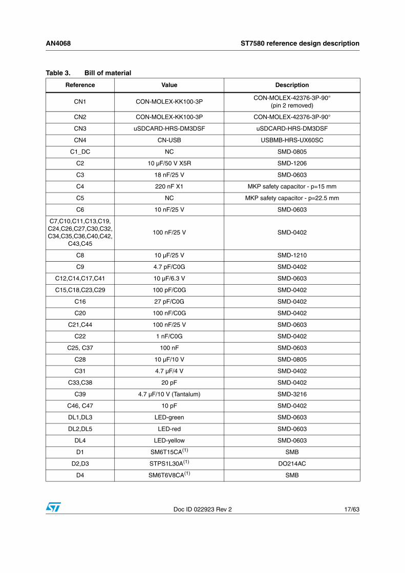
Table 3 lists the components chosen to realize the reference design board. All the parts have been selected in order to obtain good performance in a real case application.
The layout of the printed circuit board is reported in Figure 44, 45, and 46.
AN4068 ST7580 reference design description
Doc ID 022923 Rev 2 15/63
Figure 4. Schematics of the ST7580 reference design board (part 1)

ST7580 reference design description AN4068
16/63 Doc ID 022923 Rev 2
Figure 5. Schematics of the ST7580 reference design board (part 2)
C47
10pF
JP10
CLO
SEJP
11C
LOSE
M25
_QTC
K
T_REQ
BR0BR1
I2C1_SDAI2C1_SCL
MISO1
VDDIO
CLPA_IN-PA_IN+
TX_OUT
ZC_INRX_IN
PA_O
UT
SCLK0
VCC
VSSA
PLC
_RES
ETN
VDD
_REG
_1V8
VSS
GN
D
CL_
SEL
PL_T
X_O
N
PL_R
X_O
N
TXD
RXD
BR0
M25
_Q
PL_T
X_O
N
PL_R
X_O
NBR
1
CL_
SEL
8MHZ_MCO
CL_
ADC
J_TDIJ_TDOJ_TRSTN
J_TCK
STM
32_N
RST
8MH
Z_M
CO
STM
32_U
SB+
STM
32_U
SB-
PLC
_RES
ETN
PLC
_RXD
PL_R
X_O
NPL
_TX_
ON
I2C1_SDAI2C1_SCL
BOO
T1
BOO
T0
UAR
T1_R
XDU
ART1
_TXDJ_
TRST
N
J_TM
S
J_TD
OST
M32
_RES
ET#
J_TC
K
SPI2
_SC
LKSP
I2_M
ISO
BOO
T1
STM
32_U
SB+
STM
32_U
SB-
SD_C
D
SD_C
D
uSD
_SC
LKST
M32
_SD
_MIS
OST
M32
_SD
_SC
LKST
M32
_SD
_MO
SIST
M32
_SD
_NSS
uSD
_MIS
O
uSD
_NSS
uSD
_MO
SI
STM
32_S
D_M
ISO
STM
32_S
D_S
CLK
STM
32_S
D_M
OSI
STM
32_S
D_N
SS
SD_C
D
J_TMS
BOO
T0
CL_
ADC
PLC
_TXD
PLC
_T_R
EQ
I2C
1_SC
LI2
C1_
SDA
UAR
T1_T
XDU
ART1
_RXD
I2C
1_SD
AI2
C1_
SCL
MIS
O1
SPI2
_NSS
SPI2
_MO
SIJ_TD
I
TXD
TCK
SPI2
_MO
SISP
I2_M
ISO
SPI2
_SC
LKSP
I2_N
SS
RN
310
K
1 8234 5
67
R39 10K
C45100nF/25V
TP2
CL
1
C42
100n
F/25
V
C29100pF/C0G
R34
10K
R41 10K
C32
100n
F/25
V
R45
330R
C1210uF/6.3V
C34100nF/25V
TP8
TXD
1
TP4
TREQ
1
CN
4C
N-U
SB1 2 3 4
SH1SH2
5
R28NC
C35100nF/25V
C39 4.7u
F/10
V (T
ANT)
R56
4K7
1%
DL2
LED
-RED
21
R55 10K
R59
18K7
1%
J1
SPI2
CO
NN
ECTO
R
1 2 3 4 5 6
C21 100n
F/25
V
PA_O
UT
C8
10uF
/25V
R53 10K
R36
10K
SHIELD
SW5
STM
32 R
ESET
1
SH1
SH2
2
R47
10K
C10
100n
F/25
V
R48 10K
R22
100k
JTAG
1
JTAG
_20P
12
34
56
78
910
1112
1314
1516
17 1918 20
FB2
BLM
21PG
300S
N1
C40
100n
F/25
V
R32
560R
FB1
BLM
21PG
331S
N1
C37
100n
F
TP7
RXD 1
R2647K
R11
130R
R42
22R
C44
100n
F/25
V
R14
3k9
R23
10K
R25 10K
R49 10K
R2447K
DL5
LED
-RED
21
SHIELD
SW3
PUSH
_2
1
SH1
SH2
2
PA_A
DC
R50 10K
C18
100p
F/C
0G
R33 10K
R46
22R
R2947KJP8
CLO
SE
U5
USB
LC6-
2P6
I/O1#
11
GN
D2
VBU
S5
I/O2#
44
I/O1#
66
I/O2#
33
R30
10K
R37 10K
DL1
LED
-GR
EEN
21
J2
I2C
1 - U
ART1
CO
NN
ECTO
R
1 3 76 104 8
5 9
2
R13
330R
C41
10uF
/6.3
V
U4
STM
32F1
03C
BT6
PA0-
WKU
P10
PA1
11
PA2
12
PA313
PA414
PA515
PA616
PA717
PA8
29PA
930
PA10
31PA
1132
PA12
33PA
1334
PA1437 PA1538
PB018
PB119
PB220
PB339 PB10
21
PB1122
PB12
25PB
1326
PB14
27PB
1528
PB440 PB541 PB642 PB743
PB845 PB946
PC14
3
PC15
4
PD0/
OSC
-IN5
PD1/
OSC
-OU
T6
NR
ST7
BOOT044
VBAT
1
VSSA
8
VSS123
VSS2
35
VSS347
VDD
A9
VDD124
VDD
236
VDD348
PC13
/TAM
P/R
TC2
SW1
DIP
SW-4
P-90
12
43
5678
C36100nF/25V
R44
10k
C28
10uF
/10V
C46
10pF
R43
1K5
R54 10K
DL4
LED
-YEL
LOW
21
R51 10K
R52 10K
Q1
2N70
021
3 2
R35
470R
R40
470R
C1410uF/6.3V
R27100k
C30100nF/25V
C43100nF/25V
R31
560R
DL3
LED
-GR
EEN
21
CN
3uS
DC
ARD
-HR
S-D
M3D
SF
DAT
2/R
SV1
DAT
3/C
S2
CM
D/D
ATA_
IN3
VDD
4
SCLK
5
VSS2
6
DAT
0/D
ATA_
OU
T7
DAT
1/R
SV8
CDSWA COMSWB
C33
20pF
SHIELD
SW4
PUSH
_1
1
SH1
SH2
2
C11100nF/25V
JP9
STM
32 B
OO
T C
ON
FIG
124 3
SHIELD
SW2
ST75
80 R
ESET
1
SH1
SH2
2
R38
470R
Y1
8MH
z
C314.7uF/4V
FB3
BLM
21PG
600S
N1D
C27
100n
F/25
V
RN
210
K
1 8234 5
67
U3
EMIF
06-M
SD02
N16
WP/
CD
1
RD
AT3_
GN
D2
DAT
2_IN
3
DAT
3_IN
4
CM
D_I
N5
CLK
_IN
6
DAT
0_IN
7
DAT
1_IN
8
RD
ATA_
VCC
16
VCC
15
DAT
2_EX
14
DAT
3_EX
13
CM
D_E
X12
CLK
_EX
11
DAT
0_EX
10
DAT
1_EX
9
GND
EP
ST75
80
U2
RESERVED548
RESERVED447
VDD46
GND45
RESERVED344
RESERVED243
RESERVED142
PL_TX_ON41
BR040
BR139
T_REQ38
PL_RX_ON37
TXD
1
RXD
2
VDD
IO3
TRST
N4
TMS
5
GN
D6
TCK
7
TDO
8
TDI
9
RES
ETN
10
VDD
11
XIN
12
XOUT13
GND14
VSSA15
VDD_PLL16
VCCA17
ZC_IN18
RX_IN19
TX_OUT20
PA_IN+21
PA_IN-22
CL23
VCC24
CL_
SEL
36
VSSA
35
VDD
IO34
GN
D33
NC
#32
32
RES
ERVE
D0
31
NC
#30
30
NC
#29
29
VDD
IO28
VDD
_REG
_1V8
27
PA_O
UT
26
VSS
25
EP49
R18
10k
TP9
PA_A
DC
C38
20pF
R9
10K
VDD
IO
C13100nF/25V
VDD
IO
VDD
IO
VCC
A
VCC
VDD
VDD
_PLL
VDD
IO
VDD
IO
VDD
IO
VDD
IO
VDD
IO
VDD
IO
VDD
IO
VDD
IO
VDD
IO
VDD
IO
VDD
IO
VDD
IO
VDD
IO
VDD
IO
VDD
IO
STM
32_U
SB_P
WR
VDD
IO
VDD
IO
VDD
IO
VDD
IO
VDD
IO
VDD
IOVD
DIO
VDD
IO
VDD
IO
VDD
IO
VDD
IO
ST75
80 S
ECTI
ON
STM
32 S
ECTI
ON
AM11115v1
AN4068 ST7580 reference design description
Doc ID 022923 Rev 2 17/63
Table 3. Bill of material
Reference Value Description
CN1 CON-MOLEX-KK100-3PCON-MOLEX-42376-3P-90°
(pin 2 removed)
CN2 CON-MOLEX-KK100-3P CON-MOLEX-42376-3P-90°
CN3 uSDCARD-HRS-DM3DSF uSDCARD-HRS-DM3DSF
CN4 CN-USB USBMB-HRS-UX60SC
C1_DC NC SMD-0805
C2 10 µF/50 V X5R SMD-1206
C3 18 nF/25 V SMD-0603
C4 220 nF X1 MKP safety capacitor - p=15 mm
C5 NC MKP safety capacitor - p=22.5 mm
C6 10 nF/25 V SMD-0603
C7,C10,C11,C13,C19,C24,C26,C27,C30,C32,C34,C35,C36,C40,C42,
C43,C45
100 nF/25 V SMD-0402
C8 10 µF/25 V SMD-1210
C9 4.7 pF/C0G SMD-0402
C12,C14,C17,C41 10 µF/6.3 V SMD-0603
C15,C18,C23,C29 100 pF/C0G SMD-0402
C16 27 pF/C0G SMD-0402
C20 100 nF/C0G SMD-0402
C21,C44 100 nF/25 V SMD-0603
C22 1 nF/C0G SMD-0402
C25, C37 100 nF SMD-0603
C28 10 µF/10 V SMD-0805
C31 4.7 µF/4 V SMD-0402
C33,C38 20 pF SMD-0402
C39 4.7 µF/10 V (Tantalum) SMD-3216
C46, C47 10 pF SMD-0402
DL1,DL3 LED-green SMD-0603
DL2,DL5 LED-red SMD-0603
DL4 LED-yellow SMD-0603
D1 SM6T15CA(1) SMB
D2,D3 STPS1L30A(1) DO214AC
D4 SM6T6V8CA(1) SMB

ST7580 reference design description AN4068
18/63 Doc ID 022923 Rev 2
D5 LL4148 SOD80
FB1 BLM21PG331SN1 Ferrite bead SMD-0805
FB2 BLM21PG300SN1 Ferrite bead SMD-0805
FB3 BLM21PG600SN1D Ferrite bead SMD-0805
ISO1 TLP781(GB) Photo-coupler DIP4
JP1,JP2 Open Jumper SMD
JP3,JP4,JP10,JP11 Close Jumper SMD
JP5 ST7580 UART STRIP 5x1 2.54 mm male
JP6 STM32 PLC UART STRIP 3x1 2.54 mm male
JP7,JP8 Close Jumper 2x1 2.54 mm male
JP9 STM32 BOOT CONFIG Jumper 2x2 2.54 mm male 90°
JTAG1 JTAG_20P FLAT connector 10X2 male 90°
J1 SPI2 CONNECTOR STRIP 6x1 2.54 mm male
J2 I2C1 – UART1 CONNECTOR STRIP 5x2 2.54 mm male 90°
L1 15 µH EPCOS B82464-A4153K
L2 220 µH EPCOS B82462-A4224K
Q1 2N7002 SOT23
Q3 BC847C SOT23
RN2,RN3 10 kΩ RESN-CAY10
R1 NC SMD-1206
R2 0 Ω SMD-1206
R3,R4,R7,R8 56 kΩ SMD-2512
R5 150 Ω SMD-0603
R6,R20 33 kΩ SMD-0402
R9,R10,R23,R30,R34,R36,R44,R47,R48,R49,
R50,R5110 kΩ SMD-0402
R11 130 Ω SMD-0402
R12 22 kΩ SMD-0402
R13 330 Ω SMD-0402
R14 3.9 kΩ SMD-0603
R15 5.1 kΩ SMD-0402
R16 1.5 kΩ SMD-0402
R17,R19 47 kΩ SMD-0402
Table 3. Bill of material (continued)
Reference Value Description

AN4068 ST7580 reference design description
Doc ID 022923 Rev 2 19/63
R18,R25,R33,R37,R39,R41,
R52,R53,R54,R5510 kΩ SMD-0603
R21,R22 100 kΩ SMD-0603
R24,R26,R29 47 kΩ SMD-0603
R27 100 kΩ SMD-0402
R28 NC SMD-0402
R31,R32 560 Ω SMD-0402
R35,R38,R40 470 Ω SMD-0402
R42,R46 22 Ω SMD-0402
R43 1.5 kΩ SMD-0402
R45 330 Ω SMD-0402
R56 4.7 kΩ 1% SMD-0402
R57 1MEG SMD-0402
R58 24 kΩ 1% SMD-0402
R59 18.7 kΩ 1% SMD-0402
R60, R62 22 kΩ SMD-0402
SW1 DIPSW-4P-90 DIP switch 2.54 mm 4-way 90°
SW2 ST7580 RESET Push button 90°
SW3 PUSH_2 Push button 90°
SW4 PUSH_1 Push button 90°
SW5 STM32 RESET Push button 90°
TP1 PA_OUT
TP2 CL
TP3 RX_IN
TP4 T_REQ
TP5 TX_OUT
TP6 ZC_IN
TP7 RXD
TP8 TXD
TP9 PA_ADC
TP10 VSS
T1TDK SRW13EP-X05H002
/ WE 750-510-231PLC coupling transformer
U1 LK112SM33TR(1) SOT23-5
U2 ST7580(1) QFN48
Table 3. Bill of material (continued)
Reference Value Description

ST7580 reference design description AN4068
20/63 Doc ID 022923 Rev 2
7.1 Line coupling sectionThe line coupling section is made up of four different circuits: the transmission active filter, the reception passive filter, the power line coupling, and the zero crossing coupling.
All four sections are described below. For each section, calculations and measured behavior are reported.
The frequency response of the filters is usually sensitive to component value tolerance. Actual components used in the ST7580 reference design have the following tolerances: +/- 20% for the X1 capacitor and the coils, +/- 5% for SMD ceramic capacitors, +/- 1% for SMD resistors.
To evaluate sensitivity to these possible variations, simulated responses are also included, with a Montecarlo statistical analysis of response variation vs. spread of component value.
For the transmission active filter, C0G/NPO type capacitors are required to guarantee linearity and stability for any signal amplitude and frequency.
Figure 6. Line coupling section schematics
U3 EMIF06-MSD02N16(1) MicroQFN 16L 3.5x1.2 mm
U4 STM32F103CBT6(1) LQFP48
U5 USBLC6-2P6(1) SOT-666
Y1 8 MHz XTAL-HC49U
1. ST parts on board.
Table 3. Bill of material (continued)
Reference Value Description

AN4068 ST7580 reference design description
Doc ID 022923 Rev 2 21/63
7.1.1 Transmission active filter
The transmission active filter is based on the ST7580 internal power amplifier (PA), whose input and output pins are externally available to allow a filtering network tailored around the amplifier.
For the ST7580 reference design, a 3-pole low-pass filter has been realized by cascading a simple R-C low-pass stage and a Sallen-Key 2-pole cell.
The R16-C22 low-pass stage has a corner frequency at nearly 110 kHz for a first filtering of the TX_OUT harmonics. The 1 nF value of C22 has been found to be the optimal value to obtain a good filtering action without yielding unwanted capacitive load distortion on the TX_OUT line.
The transfer function of the 2nd order Sallen-Key cell is:
Equation 1
where:
Equation 2
Equation 3
Equation 4
Figure 7 represents the measured transfer function of the transmission active filter. It shows good rejection at signal harmonic frequencies.
1Q
ss
A)s(A
C2
C
20
+⋅ω
+ω
=
)RR
1(A10
60 += =4.3=12.7 db
=150 kHz
23151215C
CCRR2
1f
⋅⋅⋅⋅π=
=1.03
)A1(CRCRCR
CCRRQ
0151523151512
23151215
−++⋅⋅⋅
=

ST7580 reference design description AN4068
22/63 Doc ID 022923 Rev 2
Figure 7. Measured frequency response of the transmission active filter (typical)
A simulation of the transmission active filter response against component tolerance, depicted in Figure 8, shows +/- 1 dB variation in gain module within the signal bandwidth, while the Q variation is more sensitive around 100 kHz.
Figure 8. Montecarlo simulation of the transmission active filter frequency response

AN4068 ST7580 reference design description
Doc ID 022923 Rev 2 23/63
7.1.2 Reception passive filter
The reception filter is made up of the series of a resistor and a parallel L-C resonant. The transfer function of the filter can be written as:
Equation 5
where RL is the DC series resistance of the inductor (in this case, about 2 Ω).
The center frequency and the quality factor of the filter can be expressed as:
Equation 6
Equation 7
It is quite evident that the quality factor and the filter selectivity depend not only on the R5 value, but also on RL. Higher RL leads to lower steepness of the resonance, while higher R5 gives higher selectivity.
The RL value impacts insertion losses in a more evident way. To evaluate the relationship between RL and the received signal loss, the following simplified expression of at f=fc can be used:
Equation 8
With actual values of the components, there is a loss of about 1 dB. The same calculation gives unitary transfer if RL is set to zero.
Looking at the first way to express the module of the transfer function, it can be seen that a higher Q can help to keep the losses small. However, a high Q would bring the response to a higher sensitivity of the components' tolerance.
Figure 9 shows the measured frequency response of the Rx passive filter. The filter shows a -3 dB bandwidth equal to 65 kHz and an attenuation of less than 1 dB at fC.
325
L5
325
23L52
325
L2
CLR
RRs
CLR
LCRRs
CLR
RLs
)s(R+
+⋅+
+
+⋅
=
32325
L5C
CL2
1
CLR
RR
2
1
2
1fc
π≅
+π
=ω⋅π
= =80 kHz
C23L5
325
LCRR
CLRQ ω⋅
+= =1.3
R s( )
2
35L
5
2CC
L
CRR1
1
R
LQ)f2j(R
⋅⋅+
=⋅ω
⋅≅π⋅

ST7580 reference design description AN4068
24/63 Doc ID 022923 Rev 2
Figure 9. Measured frequency response of the reception passive filter (typical)
Figure 10 represents a simulation of the response of the Rx passive filter with component tolerance effect. The shift on center frequency gives a worst-case loss of nearly 0.5 dB at center frequency.
Figure 10. Montecarlo simulation of the reception passive filter response
7.1.3 Power line coupling
The coupling to the power line requires some passive components in addition to the active filtering stage. In particular, it includes the DC decoupling capacitor C2, the line transformer T1, the power inductor L1, and the X1 safety capacitor C4.

AN4068 ST7580 reference design description
Doc ID 022923 Rev 2 25/63
L1 has been accurately chosen to have high saturation current (>2 A) and very low equivalent series resistance (<0.1 Ω), to limit distortion and insertion losses even with heavy line load.
Center frequency for the series resonance can be calculated at first approximation as:
Equation 9
provided that the capacitance of C2 is much greater than the C4 capacitance. is the series of L1 and the leakage inductance of the coupling transformer T1, adding about 1 µH to L1.
The Q factor of this coupling circuit is driven by the mains line impedance: the choice of the L1 and C4 values, however, leads to limited attenuation due to either parasitic impedance or resonance selectivity. If loaded with 5 Ω line impedance, the coupling circuit shows a Q factor equal to 2 and a -3 dB bandwidth of 40 kHz (typical values).
Particular attention has been paid to the choice of the line transformer. The required characteristics are listed in Table 4. In order to have a good signal transfer and minimize the insertion losses, it is recommended to choose a transformer with a primary (shunt) inductance of 1 mH or greater, a leakage inductance much smaller than L1 and a total DC resistance lower than 0.5 Ω.
The 4 kV insulation voltage requirement, the last specified parameter, is described and codified by the EN50065-4-2 CENELEC document [2].
In Figure 11 the measured response of the whole transmission coupling, loaded with the LISN impedance as set by the EN50065-1 document, is reported. The image highlights a further filtering effect added by the passive L-C series resonant combined with the LISN reactive load.
Table 4. Line coupling transformer specifications
Parameter Value
Turn ratio 1:1
Shunt inductance ≥ 1 mH
Leakage Inductance ≤ 1.5 µH
DC total resistance ≤ 0.5 Ω
DC saturation current ≥ 15 mA
Inter-winding capacitance ≤ 30 pF
Withstanding voltage ≥ 4 kV
4'1 CL2
1fc
⋅π= =85 kHz
L′1

ST7580 reference design description AN4068
26/63 Doc ID 022923 Rev 2
Figure 11. Measured frequency response of the transmission line coupling loaded with the EN50065-1 LISN impedance (typical)
Figure 12 shows the coupling response with 5 Ω + 15 µF line impedance.
Figure 12. Measured frequency response of the transmission line coupling loaded with 5 Ω + 15 µF (typical)
Figure 13 represents the Montecarlo simulation of the cumulated response of transmission active and passive filters, loaded with the LISN impedance as set by the EN50065-1 document. Due to the response slope and the effect of power components, the in-band variation is within +/- 1.5 dB.

AN4068 ST7580 reference design description
Doc ID 022923 Rev 2 27/63
Figure 13. Montecarlo simulation of the transmission line coupling response loaded with the EN50065-1 LISN impedance
7.1.4 Zero crossing coupling
The zero crossing coupling circuit is aimed at providing a bipolar (AC) signal synchronous with the mains network voltage to the ZC_IN pin. This signal must be centered on VSS and limited to ± 5 V peak [1].
The isolated zero crossing circuit is realized through an optocoupler in an inverting configuration. Neutral and phase lines are brought to the optocoupler through four 56 kΩ, 1 W size SMD resistors in series, as represented in Figure 14. The LL4148 acts as a free-wheeling diode during negative half-wave. The series resistors limit the photodiode input current to nearly 1 mA rms at 230 VAC, leading to less than 250 mW of total consumption of the solution. Having two resistors per line helps to prevent short-circuits in the case of resistor degradation.
Figure 14. Isolated zero crossing coupling circuit

ST7580 reference design description AN4068
28/63 Doc ID 022923 Rev 2
The timing characteristics of this circuit, according to the oscilloscope screenshots reported below, are listed in Table 5.
Figure 15. Zero crossing coupling - positive edge delay
Figure 16. Zero crossing coupling - negative edge delay
Table 5. Zero crossing coupling - measured timing characteristics
Edge ZC delay
Positive -75 +/- 300 µs
Negative 430 +/- 300 µs
AN4068 ST7580 reference design description
Doc ID 022923 Rev 2 29/63
7.2 STM32 sectionThe EVALST7580-1 is equipped with an STM32F103CBT6 device, a medium-density ARM-based 32-bit microcontroller.
For complete information on device characteristics, please refer to [3] and [4].
On the EVALST7580-1 board, the STM32F103CBT6 microcontroller can be used for the following purposes:
● to handle the ST7580 device through direct connections
● for external access through several interface types: USB, SPI, I2C, USART, JTAG
● to store and read data to/from an external µ-SD card
● to develop test functions.
On the EVALST580-1, the STM32 microcontroller shares its VDD supply voltage with the VDDIO digital supply of the ST7580 device.
A dedicated 8 MHz crystal has been provided with two suitable load capacitors according to recommendations in [4].
7.2.1 Direct connections between STM32 microcontroller and ST7580
The STM32F103 microcontroller provides connections to the ST7580 for both digital and analog parts.
Figure 17 is an extract of the EVALST7580-1 board and it highlights the connections between the two devices only:

ST7580 reference design description AN4068
30/63 Doc ID 022923 Rev 2
Figure 17. Connections between the STM32F103CBT6 and the ST7580 devices on the EVALST80-1 board
These connections involve several pins and features of the ST7580 modem, as listed in Table 6.
Table 6. Connections between STM32F103CBT6 and ST7580 devices on EVALST80-1 board
ConnectionConnection
typeST7580 pins
STM32F103
pinsNotes
Host interface Digital
T_REQ PA1
See [2]RXD PA2
TXD PA3
Reset Digital RESETN PC15This direct connection allows the STM32 microcontroller to drive the RESETN pin
of the ST7580.
Clock Digital XIN PA8 The connection must provide an 8-MHz clock signal to the ST7580 modem in
accordance with the specifications in [1].
Power line communication
activityDigital
PL_RX_ON PC13 As the two lines give information about power line communication activity of the ST7580, the connections can be used as
input data for the STM32.PL_TX_ON PC14

AN4068 ST7580 reference design description
Doc ID 022923 Rev 2 31/63
7.2.2 Digital interfaces to the STM32
The EVALST7580-1 allows the STM32F103CB microcontroller to be accessed via its available interfaces:
● Serial wire/JTAG debug, that enables either a serial wire debug or a JTAG compliant debug through the JTAG1 connector
● USB 2.0 full speed through the mini-USB CN4 connector
● 2 SPI interfaces:
– one is used to access an external µ-SD card with FAT32 support through the µ-SD CN2 connector
– the second works at 18 Mbit/s and presents the SPI signals at the J1 strip connector
● I2C
● A second UART (TXD and RXD signals), in addition to the one used for the ST7580 connections.
I2C and UART signals are accessible through the same J2 double strip connector.
The NRST signal is externally accessible through a pushbutton.
An extract of the EVALST7580-1 board schematics for the digital interfaces of the STM32 is depicted in Figure 18:
Transmitted power line
signal levelsAnalog PA_OUT PB1
The connection allows the STM32 to monitor the ST7580’s PA_OUT voltage
level. The connection is realized through a suitable partition (between two high-value 1% tolerance resistors) to properly limit the signal level within the STM32 input
range.
CL voltage level Analog CL PA0
The connection allows the STM32 to monitor ST7580’s CL pin voltage level and to extract information about the ST7580
output current during power line transmission.
Table 6. Connections between STM32F103CBT6 and ST7580 devices on EVALST80-1 board
ConnectionConnection
typeST7580 pins
STM32F103
pinsNotes

ST7580 reference design description AN4068
32/63 Doc ID 022923 Rev 2
Figure 18. STM32F103CB external connections: schematics
AN4068 ST7580 reference design description
Doc ID 022923 Rev 2 33/63
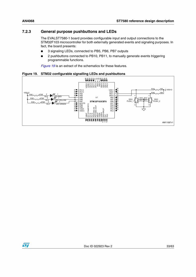
7.2.3 General purpose pushbuttons and LEDs
The EVALST7580-1 board provides configurable input and output connections to the STM32F103 microcontroller for both externally generated events and signaling purposes. In fact, the board presents:
● 3 signaling LEDs, connected to PB5, PB6, PB7 outputs
● 2 pushbuttons connected to PB10, PB11, to manually generate events triggering programmable functions.
Figure 19 is an extract of the schematics for these features.
Figure 19. STM32 configurable signalling LEDs and pushbuttons
Reference design standard tests AN4068
34/63 Doc ID 022923 Rev 2
8 Reference design standard tests
8.1 Input impedanceThe input impedance of a power line communication node is another critical point. According to the network impedance measurements carried out in certain European distribution networks (Italy, Germany and France), the following characteristics can be associated to the impedance of a typical low-voltage (LV) power line:
● Typical impedance magnitude is around 5 Ω● Nearly 90% of measured values range between 0.5 and 10 Ω● The impedance value depends on the measurement point
● The measured value changes over time.
The reasons for these characteristics can be described as follows:
● The LV distribution network has a “tree” structure, with many branches and sub-branches acting as parallel impedances
● Several electronic devices connected to the LV network offer a very low impedance, mostly because of the EMI input filters installed at their mains connection
● The type and number of electronic loads connected to the mains network varies over time.
For all these reasons, particular attention must be paid to the impedance of the ST7580 line coupling circuit. Specifically:
● In receiving (idle) mode, the coupling impedance must be high enough to make the power line source impedance negligible and to minimize the mutual interference between different PLC nodes connected to the same network
● In transmitting mode, the coupling impedance must be very low inside the signal bandwidth but high enough for out-of-band frequencies.
According to such requirements, the EN50065-7 standard document fixes the following constraints for the PLC node operating in the A band [5]:
● Tx mode:
– free in the range 3 to 95 kHz
– 3 Ω from 95 to 148.5 kHz
● Rx mode:
– 10 Ω from 3 to 9 kHz
– 50 Ω between 9 and 95 kHz only inside the signal bandwidth (free for frequencies outside the signal bandwidth)
– 5 Ω from 95 to 148.5 kHz.
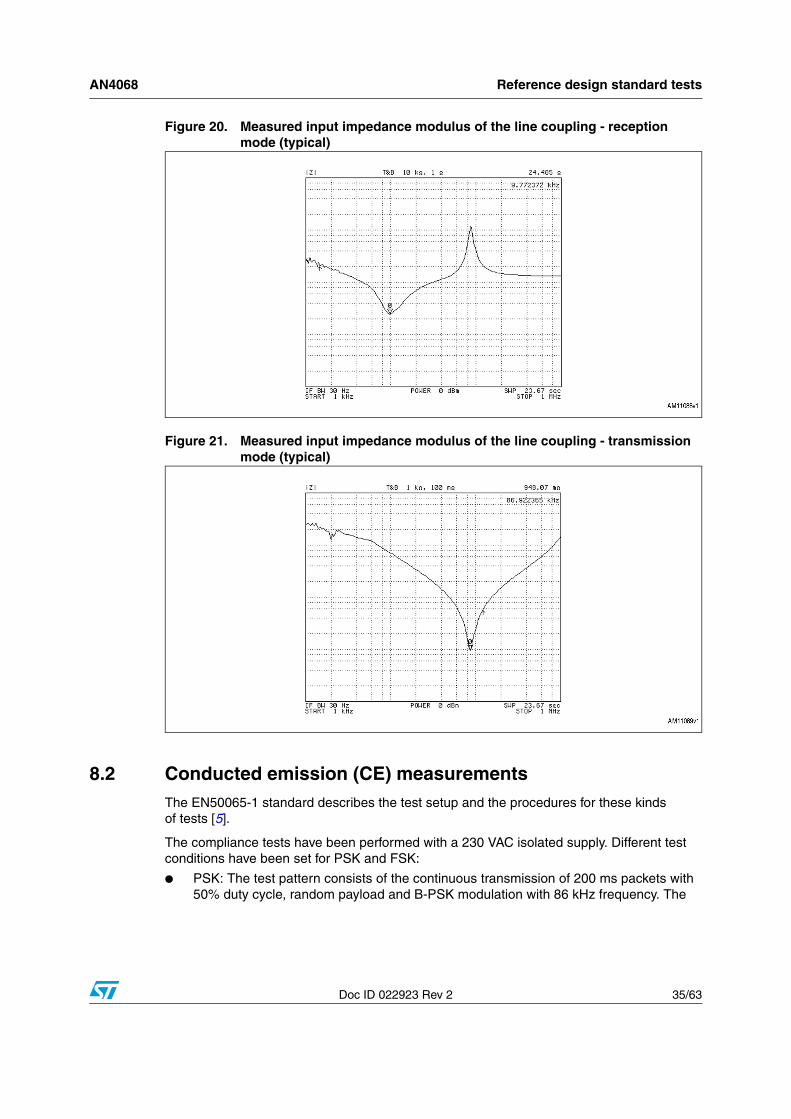
Figure 20 and 21 show the input impedance magnitude vs. frequency measured in transmission and reception mode.
The impedance magnitude values prove that the ST7580 reference design is compliant with the EN50065-7 requirements. At the same time, the line interface gives an efficient signal coupling both in transmission and reception.
AN4068 Reference design standard tests
Doc ID 022923 Rev 2 35/63
Figure 20. Measured input impedance modulus of the line coupling - reception mode (typical)
Figure 21. Measured input impedance modulus of the line coupling - transmission mode (typical)
8.2 Conducted emission (CE) measurementsThe EN50065-1 standard describes the test setup and the procedures for these kindsof tests [5].
The compliance tests have been performed with a 230 VAC isolated supply. Different test conditions have been set for PSK and FSK:
● PSK: The test pattern consists of the continuous transmission of 200 ms packets with 50% duty cycle, random payload and B-PSK modulation with 86 kHz frequency. The

Reference design standard tests AN4068
36/63 Doc ID 022923 Rev 2
output signal level has been set to nearly 9 V peak-to-peak (ST7580 TX_GAIN parameter = 26), corresponding to 127 dBµV rms.
● FSK: The test pattern consists of the continuous transmission of 200 ms packets with 50% duty cycle, random payload and FSK modulation with 82 kHz frequency at 9600 baud, deviation 1. The output signal level has been set to nearly 6 V peak-to-peak (ST7580 TX_GAIN parameter = 21), corresponding to 126 dBµV rms.
Figure 22. Conducted emissions test setup
The conducted emissions measurement results are reported below. Quasi-peak measurements have been performed, as required by the EN50065-1 standard document, for measurements above 150 kHz. Peak measurements are performed for frequencies below 150 kHz to also show the output signal level compliance. The measured spectrum is always compared to the EN50065-1 compliance limit mask.
AM11090v1

AN4068 Reference design standard tests
Doc ID 022923 Rev 2 37/63
Figure 23. Conducted emissions: PSK transmission spectrum, peak measurement, 9 kHz - 150 kHz, line-to-earth
Figure 24. Conducted emissions: PSK transmission spectrum, peak measurement, 9 kHz - 150 kHz, neutral-to-earth

Reference design standard tests AN4068
38/63 Doc ID 022923 Rev 2
Figure 25. Conducted emissions: PSK transmission spectrum, quasi-peak measurement, 150 kHz - 30 MHz, line-to-earth
Figure 26. Conducted emissions: PSK transmission spectrum, quasi-peak measurement, 150 kHz - 30 MHz, neutral-to-earth

AN4068 Reference design standard tests
Doc ID 022923 Rev 2 39/63
Figure 27. Conducted emissions: FSK transmission spectrum, peak measurement, 9 kHz - 150 kHz, line-to-earth
Figure 28. Conducted emissions: FSK transmission spectrum, peak measurement, 9 kHz - 150 kHz, neutral-to-earth

Reference design standard tests AN4068
40/63 Doc ID 022923 Rev 2
Figure 29. Conducted emissions: FSK transmission spectrum, quasi-peak measurement, 150 kHz - 30 MHz, line-to-earth
Figure 30. Conducted emissions: FSK transmission spectrum, quasi-peak measurement, 150 kHz - 30 MHz, neutral-to-earth
8.3 EMI immunity testsThe specific structure of the coupling interface circuit of the application is a weak point against high-voltage disturbances that can come from the external environment. In fact, an efficient coupling circuit with low insertion losses realizes, consequently, a low impedance path from the mains to the power line interface of the device.
For this reason it is recommended to add some specific protection on the mains coupling path, to prevent high energy disturbances coming from the mains from damaging the internal power circuitry of the ST7580.

AN4068 Reference design standard tests
Doc ID 022923 Rev 2 41/63
Possible environments for this kind of application can be both indoor and outdoor: residential, commercial and light-industrial locations. To verify the immunity of the system to environmental electrical phenomena, a series of immunity specification standards and tests must be applied to the power line application.
The immunity requirements for any PLC metering application, communicating in the European A band (9-95 kHz), are listed in the EN50065-2-3 document, which refers to EN61000 and ENV50204 for the tests to be applied [5].
These standards include surge tests, both common mode and differential mode (+/- 4 kV peak, tR = 1.2 µs, tN = 50 µs) and fast transient (burst) tests (+/- 2 kV peak, tR = 5 ns, tH = 50 ns, repetition frequency 5 kHz).
For the application to be able to withstand such a severe electrical overstress, the line coupling capacitor C4 must be an X1 or Y2 type part, rated for 4 kV or higher pulses.
In the case of non-metering applications, communicating outside the A band, the requirements are listed in the EN50065-2-1 document, which sets lower pulse levels.
In addition to the line coupling capacitor, safety and robustness of the application are guaranteed by protection devices included in the board design, such as input varistor (MOV) and protection diodes. The effect of the protection diodes is described below.
Figure 31 and 32 show the protection against common mode disturbances. The low-drop Schottky diodes D2 and D3 are able to quickly absorb fast transient disturbances exceeding the supply rails.
Figure 31. Common mode disturbance protection - positive disturbance

Reference design standard tests AN4068
42/63 Doc ID 022923 Rev 2
Figure 32. Common mode disturbance protection - negative disturbance
Figure 33 describes the protection intervention in the case of differential mode disturbances. A differential voltage higher than 15 V p-p is clamped by the D1 bi-directional Transil™ diode. D1 is the most robust protection and also the one that is able to absorb most of the energy of any incoming disturbance.
Figure 33. Differential mode disturbance protection

AN4068 Design guidelines
Doc ID 022923 Rev 2 43/63
9 Design guidelines
9.1 PCB layout guidelines
9.1.1 Thermal performance
The ST7580 device can operate within the standard industrial temperature range, from -40 to 85 °C ambient temperature. Especially in high ambient temperature conditions, the effect of the power dissipation of the device must be considered in order to keep it operating in safe conditions.
Even though the ST7580 features a built-in thermal shutdown circuitry which turns off the power amplifier (PA) when the die temperature (TJ) exceeds 150 °C, it is recommended not to exceed 125 °C during normal operation to ensure the functionality of the IC.
A QFN48 package with exposed pad has been chosen for the ST7580 device in order to obtain very good thermal performance. However, in order to take full advantage of this, the PCB must be designed to effectively conduct heat away from the package.
To get a low impedance thermal path to the PCB, a 5x5 mm thermal pad has been realized on the top layer under the device. In order to effectively remove the heat, the exposed pad must be well soldered to the PCB thermal pad. Therefore, the out-gassing phenomenon due to the soldering process must be controlled to reduce solder voids between the QFN48 exposed pad and the PCB thermal pad. To achieve this, smaller multiple openings in the solder paste stencil should be used instead of one big opening on the thermal pad region. This also has the advantage of reducing the amount of solder paste used, therefore avoiding bridges with perimeter pads.
A suitable example for the QFN48 package is shown in Figure 34.
Figure 34. Example of stencil openings for the QFN48 package
Another technique to improve heat conduction on the top layer is to fill all unused areas with copper tied to the dissipating ground plane.
In order to have an effective heat transfer from the top layer of the PCB to the bottom layer, thermal vias need to be included within the thermal pad area. If properly designed, thermal vias are the most efficient paths for removing heat from the device.

Design guidelines AN4068
44/63 Doc ID 022923 Rev 2
An array of 4 x 4 thermal vias at 1.0 mm pitch, with a via diameter of 0.3 mm, has been incorporated into the thermal pad, as shown in Figure 35.
To minimize the solder wicking effect due to open vias, possibly leading to poor soldering of the QFN48 exposed pad, the via encroaching technique has been adopted (see bottom-side image in Figure 35). The bottom-side solder resist has only small openings (nearly 0.2 mm larger than the via drill diameter) around the vias; the reduced area of exposed copper on the bottom reduces the amount of solder paste flowing down the vias.
Figure 35. PCB copper dissipating area on top layer (left) and bottom layer (right) for the ST7580 reference design board
Another important parameter for effective heat dissipation is the copper thickness for both top and bottom layers. 1 oz copper is considered as the minimum value to ensure good dissipation.
The bottom-side routing plays an important role too. The solid ground area of copper under the device must be as large as possible to minimize the thermal impedance. Therefore, traces on the bottom side must run as far as possible from the device area.
9.1.2 Ground connections
Good soldering of the ST7580 exposed pad is required also to minimize ground noise. Being the exposed pad connected to VSSA, its cleanliness is directly related to the noise level detected by the receiving circuitry (i.e. to the actual sensitivity level) and to the PLL behavior.
It is very important to filter each supply pin to its respective ground: VCC to VSS, VCCA and VDD_PLL to VSSA, VDDIO and VDD to GND.
9.2 Thermal impedance and power dissipation calculationThe relationship between junction temperature (TJ) and power dissipation during transmission (PD) is described by the following formula:

AN4068 Design guidelines
Doc ID 022923 Rev 2 45/63
Equation 10
where TA is the ambient temperature (from -40 to +85 °C) and ZthJA is the junction to ambient thermal impedance of the ST7580 IC, which is related to the length of the transmission (tTX) and to the duty cycle d = tPKT / (tPKT + tIDLE), assuming a packet-fragmented transmission as illustrated by Figure 36.
Figure 36. Packet-fragmented transmission
When soldered to a proper dissipating area on the PCB as explained above, the ST7580 IC is characterized by a steady-state thermal resistance RthJA of about 50 °C/W. The thermal impedance curve obtained as the power dissipation step response is given in Figure 37.
Figure 37. Measured ST7580 thermal impedance curve (typical)
It can be seen that the transient of ZthJA takes some thousand seconds, after which the static value of 50 °C/W is reached. This means that during the transient phase (i.e. if the transmission time tTX is some seconds or even less) the IC is able to dissipate a power that is far higher than the one sustainable at steady-state.
)d,t(ZthPT)d,t(T TXJADATXJ ⋅+=

Design guidelines AN4068
46/63 Doc ID 022923 Rev 2
For this reason, a complete thermal analysis requires that the characteristics of the transmission, i.e. duty cycle and duration, are taken into account, determining the value reached by the thermal impedance and then the allowed power dissipation.
The thermal impedance as a response to dissipation at different duty cycle and duration values can be estimated by simulating a 6-cell equivalent model obtained through the curve fitting from Figure 37, as shown in Figure 38.
Figure 38. Simulation model of the thermal impedance ZthJA of the ST7580 mounted on the reference design board
The actual dissipated power PD can be calculated as:
Equation 11
where and . Note that power consumption by the receiving circuitry and linear regulators is considered negligible for thermal analysis purposes. The relationship between current absorption from the power supply (ICC) and PA output current to the load (IOUT) is shown in Figure 2.
A transmission output level VOUT rms of 2.5 V, together with the current limit IOUT rms(LIMIT) of 1 A, corresponds to a maximum output power POUT of 2.5 W over a 1.5 Ω line load (considering a 1 Ω coupling series impedance in transmission at 86 kHz frequency). In these conditions, the required dissipation results as follows:
Equation 12
Referring to the relationship between dissipated power and temperature, it can be proved that in a continuous transmission, i.e. with ZthJA at its steady-state value of 50 °C/W, with an ambient temperature of 25 °C, the maximum dissipation can be 2 W. However, by controlling the transmission duty cycle and total duration it is possible to obtain a higher dissipation.
OUTIND PPP −=
PIN VCC= ICC⋅ POUT VOUTrms= IOUTrms⋅
W7.3)A1V5.2()A48.0V13(PPP )LIMIT(OUT)LIMIT(IN)LIMIT(D =⋅−⋅≅−=

AN4068 Design guidelines
Doc ID 022923 Rev 2 47/63
An example of communication with realistic values can be used in order to understand the point:
● B-PSK: considering 64 bytes of payload per message, the time to transmit one message is nearly 65 ms. Transmitting five messages per second, the duty cycle is 32.5%; at this rate, sending 100 messages takes 20 seconds. According to the model in Figure 38, in these conditions the ZthJA reaches 16.0 °C/W, allowing maximum dissipation PD(LIMIT) with an ambient temperature up to 66 °C.
9.3 Oscillator sectionThe ST7580 internal oscillator circuitry requires a crystal having a maximum load capacitance of 20 pF and a maximum ESR of 100 Ω. It is recommended to choose a quartz crystal with overall tolerance not greater than 150 ppm to ensure stability of carrier frequency and digital timing.
It is very important to keep the crystal oscillator and the load capacitors as close as possible to the device.
The resonant circuit must be far away from noise sources such as:
● Power supply circuitry
● Burst and surge protection
● Mains coupling circuits
● Any PCB track or via carrying an RF switching signal.
To properly shield and separate the oscillator section from the rest of the board, it is recommended to use a ground plane on both sides of the PCB, filling all the area below the crystal oscillator. No tracks or vias, except for the crystal connections, should cross the ground plane.
Connecting the case to ground may be good practice in order to reduce the effect of radiated signals on the oscillator.
9.4 Power supplyThe power supply requirements for the ST7580 reference design are listed in Table 1.
However, the power supply circuit design is not only relevant in terms of available power. Two points are particularly sensitive for a power line communication application:
● The noise injected on the line
● The input impedance of the power supply unit.
For the first point, a quasi-resonant switching mode power supply based on the ALTAIR04-900 device has been chosen. This kind of switching controller spreads the switching disturbances over a wide frequency range, therefore minimizing the overall disturbance amplitude.
The second point involves the EMI input filter design. The suggested circuit in Figure 39 has been designed to have minimum influence on the ST7580 line coupling circuit, in terms of load impedance and linearity.
The 220 nF X2 capacitor has been put close to the bridge to avoid capacitive loading on the ST7580 transmitted signal.

Design guidelines AN4068
48/63 Doc ID 022923 Rev 2
Figure 39. Example of power supply EMI input filter

AN4068 Application ideas
Doc ID 022923 Rev 2 49/63
10 Application ideas
10.1 3-phase architectureThe ST7580 modem can be used to communicate on a 3-phase network. This is especially required for low-voltage substation nodes (concentrators), collecting data from several energy meters all along the three phases of the distribution network.
In the example scheme of Figure 40, the line coupling circuit allows the signal to divide into the three phases via capacitive coupling. That structure has been designed to keep similar impedance on each phase, therefore optimizing the signal distribution between the phases.
A critical point regarding this solution may be the total impedance that the ST7580 power amplifier is required to drive, which is the result of the three phases in parallel. For concentrator nodes, however, the impedance per phase is likely to be considerably above the driving limit of the power amplifier, as all the electrical devices supplied by the power line are placed at a certain distance from the substation.
Figure 40. Scheme of principle for non-switched 3-phase architecture
In the switched coupling scheme of Figure 41, a more complex circuit is shown, being the coupling to each phase selectable via opto-switches.
Only one phase at a time can be used to transmit. The received signal, however, can be picked up from either one phase at a time (J1 closed, J2 open) or any phase at the same time (J1 open, J2 closed). Both solutions can work well: the first solution offers the advantage of reducing crosstalk between the three phases, while the second allows the whole network to be listened to at the same time. The choice depends on electrical and performance tests as well as on specific protocol requirements.

Application ideas AN4068
50/63 Doc ID 022923 Rev 2
Figure 41. Scheme of principle for switched 3-phase architecture
For the zero crossing coupling, even if only one phase at a time can be used as reference, the possibility to switch to another phase is required in case of a fault on the reference line. This can be achieved through one of the suggested circuits in Figure 42 and 43.
The external host must control the LCA715 opto-relays according to the phase status information provided by the measurement circuitry. The host controller is also responsible for ensuring that only one opto-relay is turned on, therefore guaranteeing isolation between the three phases.

AN4068 Application ideas
Doc ID 022923 Rev 2 51/63
Figure 42. 3-phase isolated zero crossing coupling circuit

Application ideas AN4068
52/63 Doc ID 022923 Rev 2
Figure 43. 3-phase non-isolated zero crossing coupling circuit
10.2 Received signal strength indication (RSSI)In many application fields, measuring the strength of the incoming signal is useful in order to:
1. Evaluate the SNR (signal to noise ratio) at the node
2. Choose the best routing through the network (if repeaters are allowed).
As explained in [1] and [2], the ST7580 embeds estimators for SNR values. These estimators are calculated during valid packet reception. The external host is notified of the values during each data indication message [2].
AN4068 FAQs and troubleshooting
Doc ID 022923 Rev 2 53/63
11 FAQs and troubleshooting
In this section the most frequently asked questions and solutions to common ST7580 reference design usage problems are described.
11.1 FAQs● Q: Is it possible to use ST power line transceivers on medium or high voltage AC lines?
– A: Yes. The same circuit solution as for low-voltage AC lines can be used, provided that the coupling interface (and particularly line transformer, power inductor and the X1 capacitor) guarantees an adequate and safe isolation from the AC line.
● Q: Is it possible to use the ST7580 on a DC or de-energized line?
– A: Yes. The ST7580 can communicate over any wired connection, given that a suitable coupling circuit is used to connect the device to the line.
● Q: Which kinds of protocols can be used with the ST7580?
– A: The ST7580 device has been conceived as an open protocol device and can be used according to the application needs. The user can develop their own protocol or use a standard one.
● Q: Does the ST7580 reference design meet FCC part 15 specs?
– A: Yes. In fact, the EN normative compliance intrinsically guarantees the compliance with FCC part 15 regulations as well.
● Q: What distance can be covered with a PLC signal?
– A: Given a transmitted signal level of 2.5 V rms, in PSK mode the ST7580 device is able to transmit through a channel attenuating up to 86 dB. This means that in a point-to-point link, a distance of several km can be covered, according to the characteristics of the line. Nevertheless, the allowable distance can be reduced because of noisy devices and low-impedance loads connected on the power line; such elements impact on the actual SNR seen by the receiver.
● Q: Why, with power line communication, can I not get 100% reachability even though the range is few meters?
– A: A probability lower than 100% to reach a PLC node within such a small distance can depend on two main factors:
a) Attenuation or losses on the power line (for example because of some heavy capacitive load connected close to the transmitter)
b) Noise coming from electric or electronic equipment connected on the power line (for example SMPS, ballasts, motors).
It may be useful to measure the signal level at transmitter and receiver to understand if there are undesired losses. It is also important to measure the noise level and spectral distribution to find out whether the PLC channel is somehow “jammed” by noise.
● Q: Does the power line communication work if a power distribution transformer is present between two nodes?
– A: The communication may work, but the transformer impedance at the signal frequency must be taken into account, as it can introduce strong attenuation in the

FAQs and troubleshooting AN4068
54/63 Doc ID 022923 Rev 2
signal level. A signal coupler (for example, a capacitive coupling) between the two sides of the distribution transformers may be required.
● Q: What method of coupling is preferred for a medium-voltage and low-voltage mains line: capacitive or inductive?
– A: For an MV line, capacitive coupling is preferable for narrow-band PLC. In the case of an LV line, having an unpredictable actual line impedance because of the number of electrical devices connected on it, the solution should be an L-C series resonant circuit tuned at channel frequency, designed to have low Q even with very low line impedance (5 Ω and below).
● Q: Is it possible to detect the channel quality through the ST7580 device?
– A: Yes. Using the ST7580 estimators for SNR, always available for the external host, it is possible to evaluate the channel quality over the physical link between transmitter and receiver.
● Q: Why use zero crossing synchronization?
– A: Zero crossing synchronization is not mandatory for the power line communication, however it has several advantages.
For instance, it can improve the communication immunity against line noise, since most of the electrical equipment generates noise on the power line in correspondence with the mains voltage peak. Zero crossing synchronization allows the establishing of the link between the transmitter and receiver during the time with the minimum time-dependent noise.
Zero crossing synchronization is also needed for 3-phase communication. In a case where one node must communicate with nodes that are connected on other phases of the mains network, zero crossing synchronization understands which phase a certain message is coming from via delta-phase calculation.
● Q: What is the minimum signal-to-noise ratio that the ST7580 can manage?
– A: A bit error rate (BER) of 10-3 is used as reference. In this condition, the ST7580 can have good receiving performance with a signal-to-noise ratio down to 3-4 dB for B-PSK coded mode.
● Q: What could be the main sources of harmonic distortion in the ST7580 transmitted signal?
– A: Generally, harmonics can increase because of:
a) High output current, due to low line impedance
b) Saturation of magnetic components in the line coupling circuit, due to either poor dimensioning of the saturation current or to 50 Hz residual current
c) Capacitive load applied to the power amplifier output
d) Insufficient margin to the supply rails (low VCC or high output voltage).

AN4068 FAQs and troubleshooting
Doc ID 022923 Rev 2 55/63
11.2 Troubleshooting1. Problem: the ST7580 reference design board doesn't work at all.
What to check:
a) Check that the AC mains supply cable is well connected.
b) Check the voltage on VCC, VDDIO, VCCA, VDD, VDD_PLL lines. All these voltages must be present to turn the ST7580 on.
c) Verify if an 8-MHz clock is present on the XOUT pin (13) of the ST7580 device.
2. Problem: the ST7580 reference design board is not responding.
What to check:
a) Check if there is activity when trying to communicate via USB with the board.
b) Try disconnecting and reconnecting the USB cable; sometimes the USB driver fails during COM port opening.
c) Try to reinstall the USB VCP driver for the STM32 on the PC.
d) Try to reprogram the STM32 with the VCP driver FW.
3. Problem: the ST7580 reference design board does not transmit.
What to check:
a) Check the bias voltage on the PA_OUT test point (TP1) with the oscilloscope probe referred to VSS power ground. A DC voltage of VCC/2 must be measured.
b) Set the ST7580 in transmission via the ST7580 GUI. A modulated signal should be detected by the oscilloscope probe, with amplitude equal to the TX_OUT programmed level multiplied by the PA gain (see Section 7.1.1). If so, there is no problem with the transmitter section of the ST7580.
4. Problem: the ST7580 reference design board transmits only for a short while; the transmission is interrupted.
What to check:
a) Verify the internal temperature of the ST7580, available inside the management information base (MIB) and accessible via the ST7580 GUI.
b) Check if there is short-circuit (i.e. capacitive) impedance on the mains at the carrier frequency. It may lead to device overheating and PA thermal shutdown.
5. Problem: the ST7580 reference design board does not receive.
What to check:
a) Check if the transmitted signal reaches the ST7580 device by measuring the RX_IN line voltage (TP5) with the oscilloscope probe referred to VSSA signal ground.
b) Check that the GUI is setting the transmitter and the receiver to use the same tone frequencies.
6. Problem: during a communication test, the ST7580 GUI shows high ‘bit error rate’ (BER).
Note: This point refers to a half-duplex communication involving two ST7580 reference design boards communicating with each other.

FAQs and troubleshooting AN4068
56/63 Doc ID 022923 Rev 2
What to check:
a) Check that both reference design boards have the same ST7580 GUI settings.
b) Verify the SNR of the communication. If the signal is too low or the noise is too high with respect to each other, the communication performance is poor. Try to:
Check the SNR estimation of the receiving ST7580 device.
Measure the signal level S and the noise level N on the RX_IN line of the receiving board.

AN4068 References
Doc ID 022923 Rev 2 57/63
12 References
1. ST7580 datasheet
2. User manual UM0932
3. STM32F103CB datasheet
4. AN2867 application note

Normative references AN4068
58/63 Doc ID 022923 Rev 2
13 Normative references
5. EN50065: signaling on low-voltage electrical installations in the frequency range 3 kHz to 148.5 kHz:
– Part 1: general requirements, frequency bands and electromagnetic disturbances
– Part 2-3: immunity requirements
– Part 4-2: low-voltage decoupling filters - safety requirements
– Part 7: equipment impedance.

AN4068 Board layout
Doc ID 022923 Rev 2 59/63
Appendix A Board layout
Figure 44. PCB layout - components
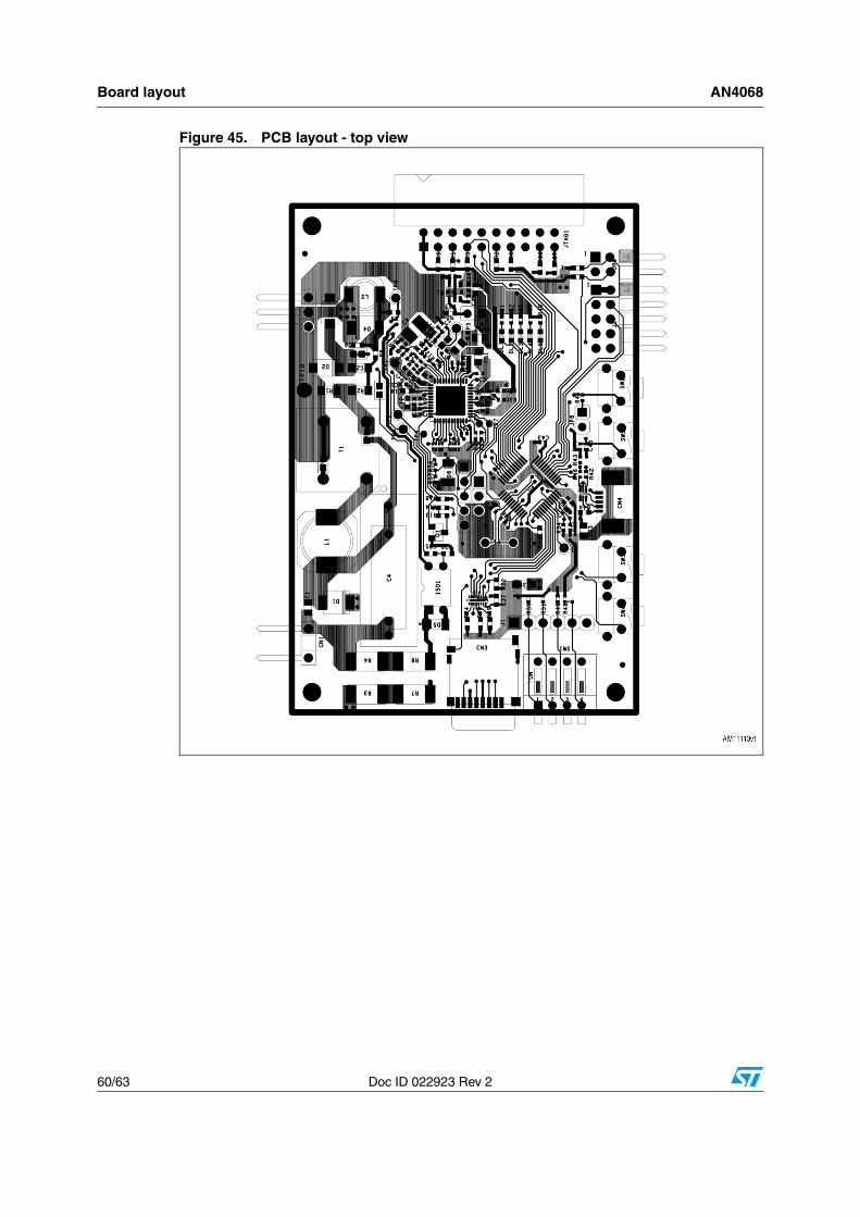
Board layout AN4068
60/63 Doc ID 022923 Rev 2
Figure 45. PCB layout - top view

AN4068 Board layout
Doc ID 022923 Rev 2 61/63
Figure 46. PCB layout - bottom view
Revision history AN4068
62/63 Doc ID 022923 Rev 2
Revision history
Table 7. Document revision history
Date Revision Changes
27-Mar-2012 1 Initial release
04-Jul-2012 2– Changed: Figure 4, 6, 14, 15 and 16– Modified: Table 3 and 5

AN4068
Doc ID 022923 Rev 2 63/63
Please Read Carefully:
Information in this document is provided solely in connection with ST products. STMicroelectronics NV and its subsidiaries (“ST”) reserve theright to make changes, corrections, modifications or improvements, to this document, and the products and services described herein at anytime, without notice.
All ST products are sold pursuant to ST’s terms and conditions of sale.
Purchasers are solely responsible for the choice, selection and use of the ST products and services described herein, and ST assumes noliability whatsoever relating to the choice, selection or use of the ST products and services described herein.
No license, express or implied, by estoppel or otherwise, to any intellectual property rights is granted under this document. If any part of thisdocument refers to any third party products or services it shall not be deemed a license grant by ST for the use of such third party productsor services, or any intellectual property contained therein or considered as a warranty covering the use in any manner whatsoever of suchthird party products or services or any intellectual property contained therein.
UNLESS OTHERWISE SET FORTH IN ST’S TERMS AND CONDITIONS OF SALE ST DISCLAIMS ANY EXPRESS OR IMPLIEDWARRANTY WITH RESPECT TO THE USE AND/OR SALE OF ST PRODUCTS INCLUDING WITHOUT LIMITATION IMPLIEDWARRANTIES OF MERCHANTABILITY, FITNESS FOR A PARTICULAR PURPOSE (AND THEIR EQUIVALENTS UNDER THE LAWSOF ANY JURISDICTION), OR INFRINGEMENT OF ANY PATENT, COPYRIGHT OR OTHER INTELLECTUAL PROPERTY RIGHT.
UNLESS EXPRESSLY APPROVED IN WRITING BY TWO AUTHORIZED ST REPRESENTATIVES, ST PRODUCTS ARE NOTRECOMMENDED, AUTHORIZED OR WARRANTED FOR USE IN MILITARY, AIR CRAFT, SPACE, LIFE SAVING, OR LIFE SUSTAININGAPPLICATIONS, NOR IN PRODUCTS OR SYSTEMS WHERE FAILURE OR MALFUNCTION MAY RESULT IN PERSONAL INJURY,DEATH, OR SEVERE PROPERTY OR ENVIRONMENTAL DAMAGE. ST PRODUCTS WHICH ARE NOT SPECIFIED AS "AUTOMOTIVEGRADE" MAY ONLY BE USED IN AUTOMOTIVE APPLICATIONS AT USER’S OWN RISK.
Resale of ST products with provisions different from the statements and/or technical features set forth in this document shall immediately voidany warranty granted by ST for the ST product or service described herein and shall not create or extend in any manner whatsoever, anyliability of ST.
ST and the ST logo are trademarks or registered trademarks of ST in various countries.
Information in this document supersedes and replaces all information previously supplied.
The ST logo is a registered trademark of STMicroelectronics. All other names are the property of their respective owners.
© 2012 STMicroelectronics - All rights reserved
STMicroelectronics group of companies
Australia - Belgium - Brazil - Canada - China - Czech Republic - Finland - France - Germany - Hong Kong - India - Israel - Italy - Japan - Malaysia - Malta - Morocco - Philippines - Singapore - Spain - Sweden - Switzerland - United Kingdom - United States of America
www.st.com


![AN4068 Application note - STMicroelectronics · CENELEC EN50065-1 standard A band, specified for automatic meter reading (AMR) applications [5]. The circuit has been designed to be](https://img.dokumen.tips/doc/110x75/610b27a30cacd026606628a3/an4068-application-note-stmicroelectronics-cenelec-en50065-1-standard-a-band.jpg)