Embed Size (px)
Citation preview
February 2011 Doc ID 16032 Rev 4 1/36
AN3009Application note
How to design a transition mode PFC pre-regulator using the L6564
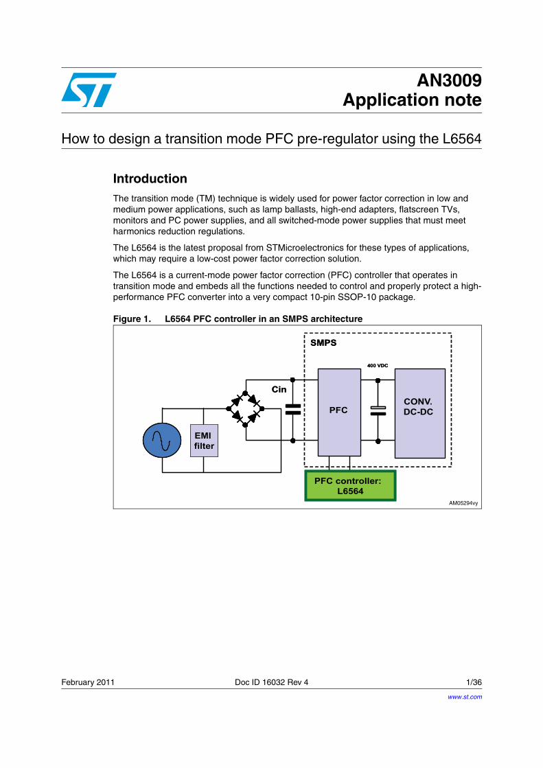
IntroductionThe transition mode (TM) technique is widely used for power factor correction in low and medium power applications, such as lamp ballasts, high-end adapters, flatscreen TVs, monitors and PC power supplies, and all switched-mode power supplies that must meet harmonics reduction regulations.
The L6564 is the latest proposal from STMicroelectronics for these types of applications, which may require a low-cost power factor correction solution.
The L6564 is a current-mode power factor correction (PFC) controller that operates in transition mode and embeds all the functions needed to control and properly protect a high-performance PFC converter into a very compact 10-pin SSOP-10 package.
Figure 1. L6564 PFC controller in an SMPS architecture
www.st.com

Contents AN3009
2/36 Doc ID 16032 Rev 4
Contents
1 Introduction to the power factor correction (PFC) . . . . . . . . . . . . . . . . . 4
2 Operating the transition mode PFC (boost topology) . . . . . . . . . . . . . . 6
3 Designing a transition mode PFC . . . . . . . . . . . . . . . . . . . . . . . . . . . . . . 8
3.1 Input specification . . . . . . . . . . . . . . . . . . . . . . . . . . . . . . . . . . . . . . . . . . . . 8
3.2 Operating conditions . . . . . . . . . . . . . . . . . . . . . . . . . . . . . . . . . . . . . . . . 10
3.3 Designing the power section . . . . . . . . . . . . . . . . . . . . . . . . . . . . . . . . . . 11
3.3.1 Rectifier bridge . . . . . . . . . . . . . . . . . . . . . . . . . . . . . . . . . . . . . . . . . . . . 11
3.3.2 Input capacitor . . . . . . . . . . . . . . . . . . . . . . . . . . . . . . . . . . . . . . . . . . . . 11
3.3.3 Output capacitor . . . . . . . . . . . . . . . . . . . . . . . . . . . . . . . . . . . . . . . . . . 12
3.3.4 Boost inductor . . . . . . . . . . . . . . . . . . . . . . . . . . . . . . . . . . . . . . . . . . . . 13
3.3.5 Power MOSFET selection and dissipation . . . . . . . . . . . . . . . . . . . . . . . 15
3.3.6 Boost diode selection . . . . . . . . . . . . . . . . . . . . . . . . . . . . . . . . . . . . . . . 18
3.4 L6564 biasing circuitry . . . . . . . . . . . . . . . . . . . . . . . . . . . . . . . . . . . . . . . 19
4 Design example using the L6564-TM PFC Excel spreadsheet . . . . . . 30
5 EVL6564-100W demonstration board . . . . . . . . . . . . . . . . . . . . . . . . . . 33
6 References . . . . . . . . . . . . . . . . . . . . . . . . . . . . . . . . . . . . . . . . . . . . . . . . 34
7 Revision history . . . . . . . . . . . . . . . . . . . . . . . . . . . . . . . . . . . . . . . . . . . 35

AN3009 List of figures
Doc ID 16032 Rev 4 3/36
List of figures
Figure 1. L6564 PFC controller in an SMPS architecture . . . . . . . . . . . . . . . . . . . . . . . . . . . . . . . . . . 1Figure 2. Boost converter circuit . . . . . . . . . . . . . . . . . . . . . . . . . . . . . . . . . . . . . . . . . . . . . . . . . . . . . 6Figure 3. Inductor current waveform and MOSFET timing. . . . . . . . . . . . . . . . . . . . . . . . . . . . . . . . . . 7Figure 4. Switching frequency fixing the line voltage . . . . . . . . . . . . . . . . . . . . . . . . . . . . . . . . . . . . . 14Figure 5. θ1 and θ2 depending on input voltage. . . . . . . . . . . . . . . . . . . . . . . . . . . . . . . . . . . . . . . . . 17Figure 6. Representation of capacitive losses . . . . . . . . . . . . . . . . . . . . . . . . . . . . . . . . . . . . . . . . . . 17Figure 7. Conduction losses and total losses in the STF7NM50N MOSFET for the L6564 TM PFC 18Figure 8. L6564 internal schematic . . . . . . . . . . . . . . . . . . . . . . . . . . . . . . . . . . . . . . . . . . . . . . . . . . 19Figure 9. Open-loop transfer function bode plot . . . . . . . . . . . . . . . . . . . . . . . . . . . . . . . . . . . . . . . . 23Figure 10. Phase . . . . . . . . . . . . . . . . . . . . . . . . . . . . . . . . . . . . . . . . . . . . . . . . . . . . . . . . . . . . . . . . . 23Figure 11. Multiplier characteristics for VFF =1 V. . . . . . . . . . . . . . . . . . . . . . . . . . . . . . . . . . . . . . . . . 24Figure 12. Multiplier characteristics for VFF = 3 V . . . . . . . . . . . . . . . . . . . . . . . . . . . . . . . . . . . . . . . . 24Figure 13. Optimum MOSFET activation . . . . . . . . . . . . . . . . . . . . . . . . . . . . . . . . . . . . . . . . . . . . . . . 28Figure 14. Excel spreadsheet design specification input table . . . . . . . . . . . . . . . . . . . . . . . . . . . . . . 30Figure 15. Other design data . . . . . . . . . . . . . . . . . . . . . . . . . . . . . . . . . . . . . . . . . . . . . . . . . . . . . . . . 30Figure 16. Excel spreadsheet TM PFC schematic. . . . . . . . . . . . . . . . . . . . . . . . . . . . . . . . . . . . . . . . 31Figure 17. Excel spreadsheet BOM - 100 W TM PFC based on L6564 . . . . . . . . . . . . . . . . . . . . . . . 32Figure 18. Wide-range 100 W demonstration board electrical circuit (EVL6564-100W) . . . . . . . . . . . 33
Introduction to the power factor correction (PFC) AN3009
4/36 Doc ID 16032 Rev 4
1 Introduction to the power factor correction (PFC)
The front-end stage of conventional offline converters, typically consisting of a full-wave rectifier bridge with a capacitor filter, has an unregulated DC bus from the AC mains. The filter capacitor must be large enough to have a relatively low ripple superimposed on the DC level. This means that the instantaneous line voltage is below the voltage on the capacitor most of the time, thus the rectifiers conduct only for a small portion of each line’s half-cycle.
The current drawn from the mains then becomes a series of narrow pulses whose amplitude is five to ten times higher than the resulting DC value. Many drawbacks result, such as a much higher peak and RMS current down from the line, distortion of the AC line voltage, overcurrents in the neutral line of the three-phase systems and, consequently, poor utilization of the power system's energy capability. This can be measured in terms of either total harmonic distortion (THD), as norms provide for, or power factor (PF), intended as the ratio between the real power (the one transferred to the output) and the apparent power (RMS line voltage times RMS line current) drawn from the mains, which is more immediate. A traditional input stage with capacitive filter has a low PF (0.5-0.7) and a high THD (>100%).
By using switching techniques, a power factor correction (PFC) pre-regulator, located between the rectifier bridge and the filter capacitor, allows drawing a quasi-sinusoidal current from the mains, in phase with the line voltage. The power factor becomes very close to 1 (more than 0.99 is possible) and the previously mentioned drawbacks are eliminated. Theoretically, any switching topology can be used to achieve a high power factor but, in practice, the boost topology has become the most popular thanks to the advantages it offers.
Primarily because the circuit requires the fewest external parts (low-cost solution).
The boost inductor located between the bridge and the switch causes the input di/dt to be low, thus minimizing the noise generated at the input and, therefore, the requirements on the input EMI filter.
The switch is source-grounded, therefore easy to drive.
However, a boost topology requires the DC output voltage to be higher than the maximum expected line peak voltage (400 VDC is a typical value for 230 V or wide-range mains applications). In addition, there is no isolation between the input and output, thus any line voltage surge is passed on to the output. Two methods of controlling a PFC pre-regulator are currently widely used: the fixed-frequency average current mode pulse-width modulation (FF PWM) and the transition mode pulse-width modulation (TM PWM), the latter having a fixed ON time and variable frequency. The first method needs a complex control that requires a sophisticated controller IC (ST's L4981A, with the variant of the frequency modulation offered by the L4981B) and a considerable component count. The second method requires a simpler control (implemented by ST's L6564), fewer external parts and is therefore much more economical. With the first method, the boost inductor works in continuous conduction mode, while the transition mode makes the inductor work on the boundary between continuous and discontinuous mode by definition. For a given throughput power, transition mode operation involves higher peak currents. This, also consistently with cost considerations, suggests its use in a lower power range (typically up to 250 W), while the former is recommended for higher power levels. To conclude, FF PWM is not the only alternative when continuous current mode (CCM) operation is desired. FF PWM modulates both switch ON and OFF times (their sum is constant by definition), and a given converter operates in either CCM or DCM (discontinuous current mode), depending on the input voltage and the load conditions.

AN3009 Introduction to the power factor correction (PFC)
Doc ID 16032 Rev 4 5/36
Exactly the same result can be achieved if the ON time only is modulated and the OFF time is kept constant, in which case, however, the switching frequency is no longer fixed. This is referred to as “fixed off time” (FOT) control. Peak current-mode control can still be used. This application note focuses on transition mode.
Operating the transition mode PFC (boost topology) AN3009
6/36 Doc ID 16032 Rev 4
2 Operating the transition mode PFC (boost topology)
The operation of the PFC transition mode controlled boost converter can be summarized as follows.
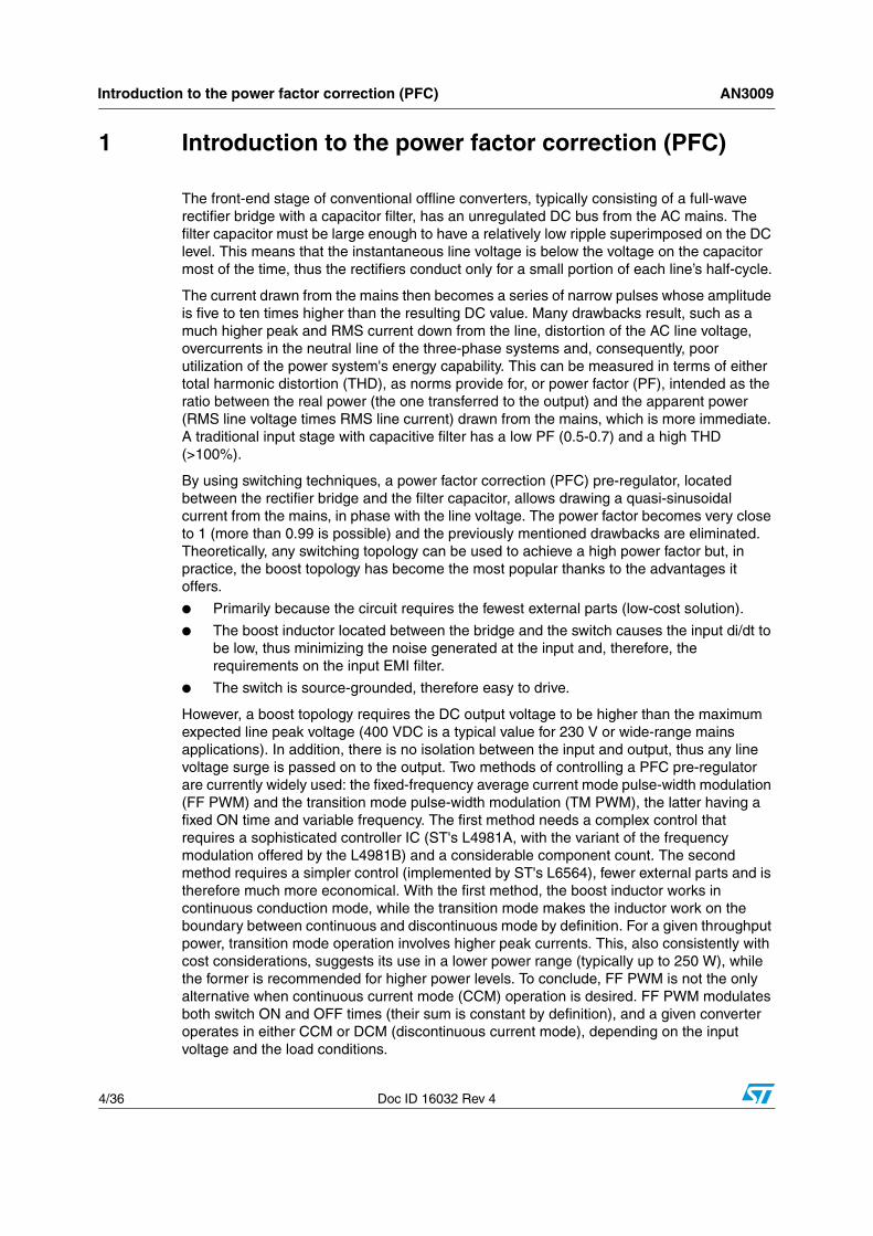
The AC mains voltage is rectified by a bridge and this rectified voltage is delivered to the boost converter. This boost converter, using a switching technique, boosts the rectified input voltage to a regulated DC output voltage (Vo).
The boost converter consists of a boost inductor (L), a controlled power switch (Q), a catch diode (D), an output capacitor (Co) and, obviously, a control circuitry (Figure 2). The goal is to shape the input current in a sinusoidal fashion, in phase with the input sinusoidal voltage. To do this, the L6564 uses the transition mode technique.
Figure 2. Boost converter circuit
The error amplifier compares a partition of the output voltage of the boost converter with an internal reference, generating an error signal proportional to the difference between them. If the bandwidth of the error amplifier is narrow enough (below 20 Hz), the error signal is a DC value over a given half-cycle.
The error signal is fed into the multiplier block and multiplied by a partition of the rectified mains voltage. The result is a rectified sinusoid whose peak amplitude depends on the mains peak voltage and the value of the error signal.
The output of the multiplier is in turn fed into the (+) input of the current comparator, thus it represents a sinusoidal reference for the PWM. In fact, when the voltage on the current sense pin (instantaneous inductor current times the sense resistor) equals the value on the (+) of the current comparator, the conduction of the MOSFET is terminated. As a consequence, the peak inductor current is enveloped by a rectified sinusoid. As demonstrated in Section 3.3.4, transition mode control causes a constant ON time operation over each line half-cycle.
After the MOSFET has been turned off, the boost inductor discharges its energy into the load until its current goes to zero. The boost inductor has now run out of energy, the drain node is floating and the inductor resonates with the total capacitance of the drain. The drain voltage drops rapidly below the instantaneous line voltage and the signal on the zero current detector (ZCD) drives the MOSFET on again and another conversion cycle starts.
This low voltage across the MOSFET upon its activation reduces both the switching losses and the total drain capacitance energy that is dissipated inside the MOSFET.
AN3009 Operating the transition mode PFC (boost topology)
Doc ID 16032 Rev 4 7/36
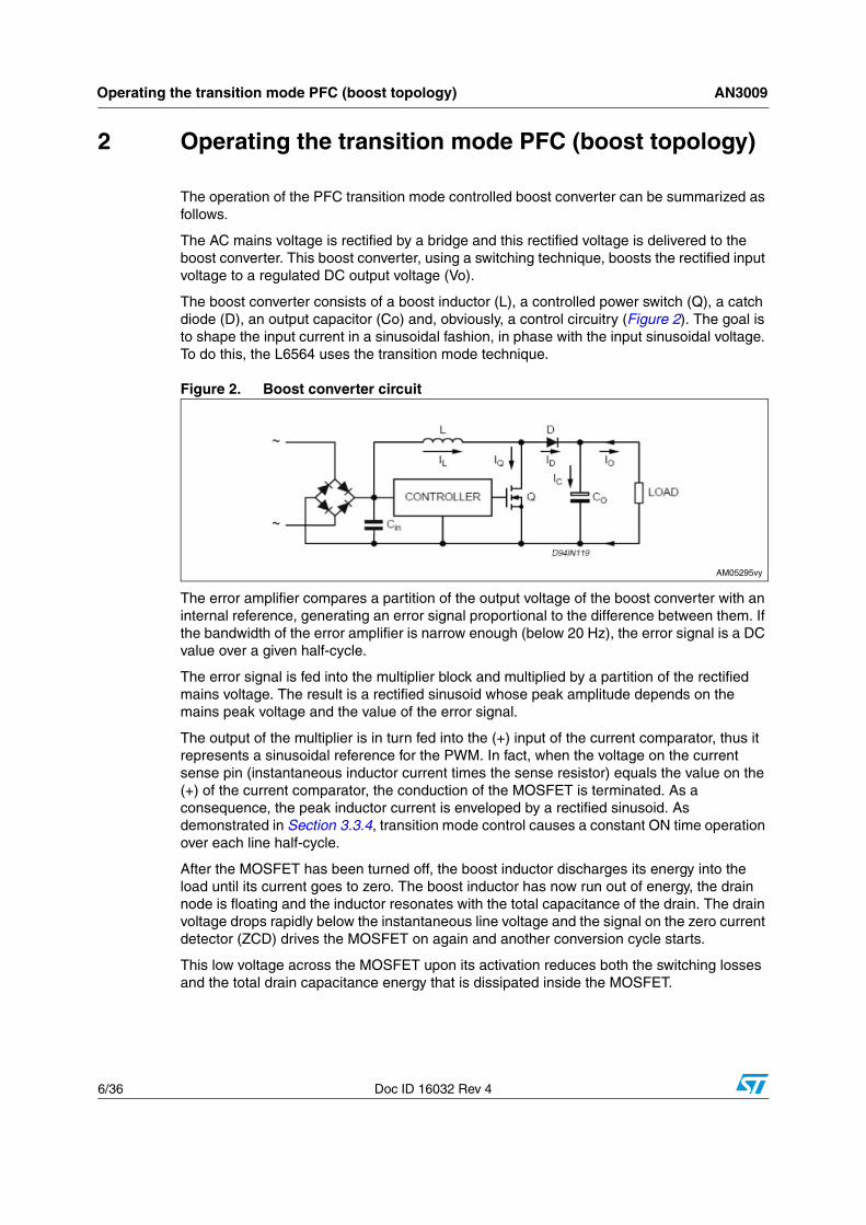
The resulting inductor current and the timing intervals of the MOSFET are shown in Figure 3, where it can be observed that, by geometric relationships, the average input current (the one drawn from the mains) is just one half of the peak inductor current waveform.
Figure 3. Inductor current waveform and MOSFET timing
The system operates not exactly on, but very close to, the boundary between continuous and discontinuous current mode and that is why this system is called a transition mode PFC. Besides the simplicity and the few external parts required, this system minimizes the inductor’s size due to the low inductance value needed. On the other hand, the high current ripple on the inductor involves high RMS current and high noise on the rectified mains bus, which needs a heavier EMI filter to be rejected. These drawbacks limit the use of the TM PFC to lower power range applications.

Designing a transition mode PFC AN3009
8/36 Doc ID 16032 Rev 4
3 Designing a transition mode PFC
3.1 Input specificationThis sections describes a possible design flowchart referred to as a transition mode PFC, using the L6564. The first part is a detailed specification of the operating conditions of the circuit that is needed for the following calculation. In this example, a L6564 wide input range mains PFC circuit has been considered. Some design criteria is also provided.
Because the PFC has a boost topology, the regulated output voltage depends strongly on the maximum AC input voltage. In fact, for correct operation of the boost mechanism the output voltage must always be higher than the input. As a result, because Vin max is 265.1.414 = 374.7 Vpk, the typical value of the output has been set to 400 Vdc. If the input voltage is higher, as is typical in ballast applications, the output voltage must be increased accordingly. As a rule of thumb, the output voltage must be 6 or 7% higher than the maximum input voltage peak.
The target efficiency and power factor are set here to the minimum input voltage and maximum load. They are used for the following operating condition calculation of the PFC. Of course, at high input voltages the efficiency is higher.
Because of the narrow-loop voltage bandwidth, the PFC output can face overvoltages at start-up or when load transients occur.
To avoid excessive output voltages that might overstress the output components and the load, the L6564 incorporates a device pin (PFC_OK, pin #6) dedicated to monitoring the output voltage with a separate resistor divider, selected so that the voltage at the pin reaches 2.5 V if the output voltage exceeds a preset value (VOVP), usually larger than the maximum Vout that can be expected (including worst-case load/line transients).
Mains voltage range (Vac rms):
(1)
Minimum mains frequency
(2)
Rated output power (W):
(3)
Regulated DC output voltage (Vdc):
(4)
Expected efficiency (%):
(5)
Expected power factor:
(6)
Vac90VACmin = Vac265VACmax =
Hz47fl =
W100Pout =
V400Vout =
%94=η
99.0PF =

AN3009 Designing a transition mode PFC
Doc ID 16032 Rev 4 9/36
The mains frequency generates a 2 fL voltage ripple on the output voltage at full load. The ripple amplitude determines the current flowing into the output capacitor and the ESR.
Additionally, a request for a certain hold-up capability can be sent to the PFC in case mains dips occur, in which case the output capacitor also has to be dimensioned taking into account the required minimum voltage value (Vout min) after the hold-up time (tHold) has elapsed.
The PFC’s minimum switching frequency is one of the main parameters used to dimension the boost inductor; here the switching frequency is considered at low mains at the peak of the sinusoid and at full load conditions. As a rule of thumb, the switching frequency must be higher than the audio bandwidth to prevent audible noise. Additionally, it must not interfere with the L6564’s minimum internal starter period (reported in the datasheet). On the other hand, if the minimum frequency is too high, the circuit shows excessive losses at a higher input voltage and probably skips switching cycles not only at light loads. The typical minimum frequency range is 20 - 50 kHz for wide-range operation.
To properly select the power components of the PFC and dimension the heatsinks if they are needed, the maximum operating ambient temperature around the PFC circuitry must be known. Note that this is not the maximum external operating temperature of the entire equipment, but rather the local temperature at which the PFC components are working.
Maximum output voltage (Vdc):
(7)
Maximum output low frequency ripple:
(8)
Minimum output voltage after line drop (Vdc):
(9)
Holdup capability (ms):
(10)
Minimum switching frequency (kHz):
(11)
Maximum ambient temperature (°C):
(12)
V430VOVP =
V20Vout =∆
V300V minout =
ms10tHold =
kHz40f minsw =
C50Tambx °=
Designing a transition mode PFC AN3009
10/36 Doc ID 16032 Rev 4
3.2 Operating conditionsThe first step is to define the main parameters of the circuit, using the specification points defined in the previous section.
Rated DC output current
Equation 1
Maximum input power
Equation 2
RMS input current
Equation 3
Peak inductor current
Equation 4
As shown in Figure 3 on page 7, the inductor current is of a triangular shape at the switching frequency, and the peak of the triangle is twice its average value. The average value of the inductor current is exactly the peak of the input sinewave current, and therefore can be easily calculated as its RMS value can be obtained from Equation 3. To write a complete inductor specification for the inductor manufacturer, one also must provide the RMS and AC current, which can both be calculated from Equation 5 and Equation 6, respectively.
RMS inductor current
Equation 5
AC inductor current
Equation 6
The current flowing in the inductor can be split into two parts, depending on the instant of conduction: during the ON time, the current increases from zero up to the peak value and circulates into the switch, while during the following OFF time, the current decreases from the peak down to zero and circulates into the diode. Therefore, a current with a triangular wave flows into these two components with a peak value equal to the inductor value. It is also possible, therefore, to calculate the RMS current flowing into the switch and into the diode, which is necessary to calculate the losses of these two elements.
out
outout V
PI = A25.0
V400W100
Iout ==
η= out
inP
P W38.10610094
W100Pin =⋅=
PFVACP
Imin
inin ⋅
= A19.199.0Vac90
W38.106Iin =
⋅=
inpk I22IL ⋅⋅= A38.3A19.122ILpk =⋅⋅=
inrms I3
2IL ⋅= A38.1A19.1
3
2ILrms =⋅=
2in
2rmsac IILIL −= ( ) ( ) A69.0A19.138.1IL 22
ac =−=

AN3009 Designing a transition mode PFC
Doc ID 16032 Rev 4 11/36
RMS switch current
Equation 7
RMS diode current
Equation 8
3.3 Designing the power section
3.3.1 Rectifier bridge
The input rectifier bridge can use any standard, slow recovery, low-cost device. A 600 V device is normally used to obtain enough margin against mains surges. A negative temperature coefficient (NTC) resistor limiting the current at turn-on is required to prevent any overstress on the diode bridge.
The power dissipation of the rectifier bridge can be calculated using Equation 9, Equation 10 and Equation 11. The threshold voltage and dynamic resistance of a single diode of the bridge can be found in the component datasheet.
Equation 9
Equation 10
For this application, a GBU4J rectifier bridge has been used. The power dissipated by the bridge is:
Equation 11
3.3.2 Input capacitor
The input high-frequency filter capacitor (Cin) has to attenuate the switching noise due to the high-frequency inductor current ripple (twice the average line current, as shown in Figure 3). The worst conditions occur on the peak of the minimum rated input voltage. The maximum high-frequency voltage ripple across Cin is usually imposed between 5% and 20% of the minimum rated input voltage. This is expressed by a coefficient r (= 0.05, 0.2) as an input design parameter.
out
minpkrms V
VAC9
2461
ILISW ⋅π
⋅−⋅= A18.1V400
Vac909
2461
A38.3ISWrms =⋅π
⋅−⋅=
out
minpkrms V
VAC9
24ILID ⋅
π⋅⋅= A72.0
V400Vac90
924
A38.3IDrms =⋅π
⋅⋅=
A84.02
A19.122
I2I ininrms =⋅=⋅=
A54.0A19.12I2
I inavg_in =
π⋅=
π⋅=
avg_inthinrms2
diodebridge IV4IR4P ⋅⋅+⋅⋅=
W62.1A54.0V7.04)A84.0(04.04P 2bridge =⋅⋅+⋅Ω⋅=

Designing a transition mode PFC AN3009
12/36 Doc ID 16032 Rev 4
Equation 12
In real conditions, the input capacitance must be designed taking into account the EMI filter and a tolerance on the component of about 5% to 10% (typical for polyester capacitors).
A commercial value of Cin = 0.47 µF has been selected. Of course, a larger capacitor provides a benefit from an EMI point-of-view, but does not benefit the THD, especially at high mains. Therefore, a compromise must be found between these two parameters. A good-quality film capacitor for this component must be selected to provide effective filtering.
3.3.3 Output capacitor
The selection of the output bulk capacitor (Co) depends on the DC output voltage (4), the allowed maximum output voltage (7) and the converter’s output power (3).
The 100/120 Hz (twice the mains frequency) voltage ripple (∆Vout = peak-to-peak ripple value) is a function of the capacitor impedance and the peak capacitor current.
Equation 13
With a low ESR capacitor the capacitive reactance is dominant, therefore:
Equation 14
∆Vout is usually selected in the range of 1.5% of the output voltage. Although ESR does not normally affect the output ripple, it should be taken into account to calculate the power losses. The total RMS capacitor ripple current, including mains frequency and switching frequency components, is:
Equation 15
If the PFC stage has to guarantee a specified hold-up time, the selection criterion of the capacitance changes: Co has to deliver the output power for a certain time (tHold) with a specified maximum dropout voltage (Vout min), that is, the minimum output voltage value (which takes load regulation and output ripple into account) and is the minimum output operating voltage before the 'power fail' detection and consequent stopping by the downstream system supplied by the PFC.
Ripple voltage coefficient (%):
(13)r 0.15=
minminsw
inin VACrf2
IC
⋅⋅⋅π= F359.0
Vac9015.0kHz402A19.1
Cin µ=⋅⋅⋅π
=
22
Oloutout ESR
)Cf22(
1I2V +
⋅⋅π⋅⋅=∆
outoutl
out
outl
outO VVf2
P
Vf2
IC
∆⋅⋅⋅π=
∆⋅⋅π≥ F5.42
V20V400Hz472W100
CO µ=⋅⋅⋅π
≥
2outrms
2Crms IIDI −= ( ) ( ) A67.0A25.0A72.0I 22
Crms =−=

AN3009 Designing a transition mode PFC
Doc ID 16032 Rev 4 13/36
Equation 16
A 20% tolerance on the electrolytic capacitors has to be considered to obtain the correct dimensioning. As per Equation 14, we have selected for this application a capacitor Co equal to 47 µF (450 V) so as to maintain a hold-up capability for 12 ms. The actual output voltage ripple with this capacitor is also calculated. In detail:
Equation 17
As expected the ripple variation on the output is:
Equation 18
3.3.4 Boost inductor
The boost inductor determines the working frequency of the converter, thus it is usually calculated so that the minimum switching frequency is greater than the maximum frequency of the L6564’s internal starter (typically 150 µs) to ensure correct transition mode operation. Assuming a unity power factor, it is possible to write:
Equation 19
Equation 19 shows that the ON time does not depend on the angle of the mains phase, but is constant over the entire mains cycle.
Equation 20
ton and toff are the power MOSFET’s ON and OFF times respectively, ILpk the maximum peak inductor current in a line cycle and θ the instantaneous line phase in the interval [0,Π]). Note that the ON time is constant over a line cycle.
As previously said, ILpk is twice the line-frequency peak current (Equation 4), which is related to the input power and input mains voltage. By substituting this relationship in the expressions of ton and toff, it is possible to find the instantaneous switching frequency along a given line cycle.
( ) 2minout
2outout
HoldoutO
VVV
tP2C
−∆−
⋅⋅=
( ) ( )F7.36
V300V20V400
ms10W1002C
22O µ=−−
⋅⋅=
( )out
2minout
2outoutO
hold P2
VVVCt
⋅⎥⎦⎤
⎢⎣⎡ −∆−⋅
=( ) ( )[ ]
ms78.14W1002
V300V20V400F47t
22
hold =⋅
−−⋅µ=
Ol
outout Cf2
IV
⋅⋅π⋅=∆ V02.18
F47Hz472A25.0
Vout =µ⋅⋅π⋅
=∆
VAC2
ILL
)sin(VAC2
)sin(ILL),VAC(t pkpk
on⋅
⋅=
ϑ⋅⋅
ϑ⋅⋅=ϑ
)sin(VAC2V
)sin(ILL),VAC(t
out
pkoff
ϑ⋅⋅−
ϑ⋅⋅=ϑ

Designing a transition mode PFC AN3009
14/36 Doc ID 16032 Rev 4
Equation 21
The switching frequency is minimal at the top of the sinusoid (θ = Π /2 ==> sin θ =1), maximal at the zero crossings of the line voltage (θ = 1 or Π ==> sin θ =0), where toff = 0.
The absolute minimum frequency fswmin can occur at either the maximum VACmax or the minimum mains voltage VACmin. The inductor value is therefore defined by the formula:
Equation 22
After calculating the values of the inductor at low and high mains – L(VACmin) and L(VACmax) – the minimum value must be taken into account. It becomes the maximum inductance value for dimensioning the PFC.
Equation 23
For this application, a 0.52 mH boost inductance has been selected.
Figure 4. Switching frequency fixing the line voltage
Figure 4 shows the switching frequency versus the θ angle calculated with Equation 22, a 0.52 mH boost inductance and the line voltage fixed at the minimum and maximum values. The minimum switching frequency can be recalculated for the selected inductance value by inverting Equation 22 to become:
Equation 24
( )out
out2
inoffonsw V
)sin(VAC2VVAC
PL21
TT1
),VAC(fθ⋅⋅−⋅
⋅⋅⋅
=+
=θ
outinminsw
out2
VPf2
)VAC2V(VAC)VAC(L
⋅⋅⋅⋅−⋅
=
( )mH642.0
V400W38.106kHz402)Vac902V400(Vac90
)VAC(L2
min =⋅⋅⋅⋅−⋅=
( )mH515.0
V400W38.106kHz402)Vac2652V400(Vac265
)VAC(L2
max =⋅⋅⋅⋅−⋅=
outin
out2
minsw VPL2
)VAC2V(VAC)VAC(f
⋅⋅⋅⋅−⋅
=
AN3009 Designing a transition mode PFC
Doc ID 16032 Rev 4 15/36
When one compares fswmin(VACmin) and fswmin(VACmax) with L = 0.52 mH, the actual calculated minimum switching frequency is 40.13 kHz, as expected.
The core size is determined by assuming a peak flux density Bx ≅ 0.25 T (depending on the ferrite grade selected and relevant specific losses) and by calculating the maximum current according to Equation 45, as a function of the maximum clamping voltage of the current sense pin and the value of the sense resistor.
DC and AC copper losses and ferrite losses must also be calculated to determine the maximum temperature rise of the inductor.
3.3.5 Power MOSFET selection and dissipation
The MOSFET selection involves mainly its RDS(on), which depends on the output power (3), since the breakdown voltage is fixed by the output voltage only (4), plus the overvoltage allowed (7) and a safety margin (20%). Therefore, a voltage rating of 500 V (1.2 · Vout = 480 V) has been selected. With regard to its current rating, as a rule of thumb, one can select a device with approximately three times the RMS switch current (Equation 7) but, in any case, the calculation of the power dissipation provides the final confirmation that the selected device is the right one for the circuit. The heatsink dimensions must also be taken into consideration. For this L6564 TM PFC application, we have selected a STF7NM50 MOSFET. The MOSFET's power dissipation depends on the conduction, switching and capacitive losses.
The conduction losses at maximum load and minimum input voltage are calculated by:
Equation 25
Since in datasheets the RDS(on) is normally given at ambient temperature (25 °C), to correctly calculate the conduction losses at 100°C (typical MOSFET junction working temperature), a factor of 1.75-2 should be applied. The correct factor can be found in the device datasheet.
The conduction losses referred to a 1 Ω RDS(on) at ambient temperature as a function of the input power (pin) and Vac can now be calculated by combining Equation 25 and Equation 7.
Equation 26
The switching losses in the MOSFET occur only at turn-off because of the TM operation, and can be basically expressed by:
Equation 27
Equation 27 represents the crossing between the MOSFET current that decreases linearly during the fall time and the voltage on the MOSFET drain that increases. In fact, during the fall time, the current of the boost inductor flows into the parasitic capacitance of the MOSFET charging it.
( )2rms)on(DScond )VAC(ISWR)VAC(P ⋅=
2
out
in2rmscond V
VAC2316
2PFVAC2
P2))VAC(ISW(2)VAC(P ⎟
⎟
⎠
⎞⎜⎜
⎝
⎛ ⋅⋅π
−⋅⋅⋅
⋅=⋅=′
)VAC(ftIV)VAC(P swfallMOSMOSswitch ⋅⋅⋅=

Designing a transition mode PFC AN3009
16/36 Doc ID 16032 Rev 4
For this reason, switching losses also depend on the total drain capacitance. Because the switching frequency depends on the input line voltage and the phase angle on the sinusoidal waveform, using Equation 27 the switching losses per 1 µs of current fall time and 1 nF of total drain capacitance can be written as:
Equation 28
Refer to the MOSFET datasheet to find the value of tfall at turn-off.
At turn-on, the losses are due to the discharge of the total drain capacitance inside the power MOSFET itself. In general, the capacitive losses are given by:
Equation 29
where Cd is the total drain capacitance including the MOSFET and any other parasitic capacitances such as the inductor at the drain node, and where VMOS is the drain voltage at the MOSFET’s turn-on.
Taking into account the frequency variation with the input line voltage and the phase angle similar to Equation 29, a detailed description of the capacitive losses per 1 nF of total drain capacitance can be calculated as:
Equation 30
θ and θ2 depend on the input voltage and are defined below.
Equation 31
Equation 32
( )∫π
ϑ⋅θ⋅ϑπ
⋅⋅=′0
sw2
outpkswitch d),VAC(fsin1
VIL)VAC(P
)VAC(fVC21
)VAC(P swMOS2
dcap ⋅⋅⋅=
( ) ϑ⋅ϑ−π
⋅=′ ∫ϑ
ϑ
d),VAC(fVVAC221
21
)VAC(P2
sw2
outcap
1
⎟⎟⎠
⎞⎜⎜⎝
⎛=ϑ
VAC22
Varcsin out
1
12 ϑ−π=ϑ

AN3009 Designing a transition mode PFC
Doc ID 16032 Rev 4 17/36
Figure 5 shows the relationship between θ1 and θ2 depending on the input voltage. Figure 6 represents a waveform of the drain voltage. The MOSFET’s activation occurs exactly on the valley because the inductor has run out of energy and therefore can resonate with the drain capacitance. Details are provided in the section on the ZCD pin (pin #7). It is clear that for an input voltage theoretically lower than half of the output voltage, the resonance should ideally reach zero, achieving a zero voltage operation and therefore avoiding any losses on this edge. An input voltage corresponding to a positive value of the valley generates capacitive losses. However, activation of the MOSFET always occurs at the minimum voltage of the resonance and therefore the losses are minimized.
In practice, it is possible to estimate the total switching and capacitive losses by solving the integral of the switching frequency depending on sin(θ) on the half-line cycle.
The total losses function of the input mains voltage is the sum of the three previous losses’ functions (Equation 26, Equation 28 and Equation 30 respectively) multiplied by the MOSFET parameters.
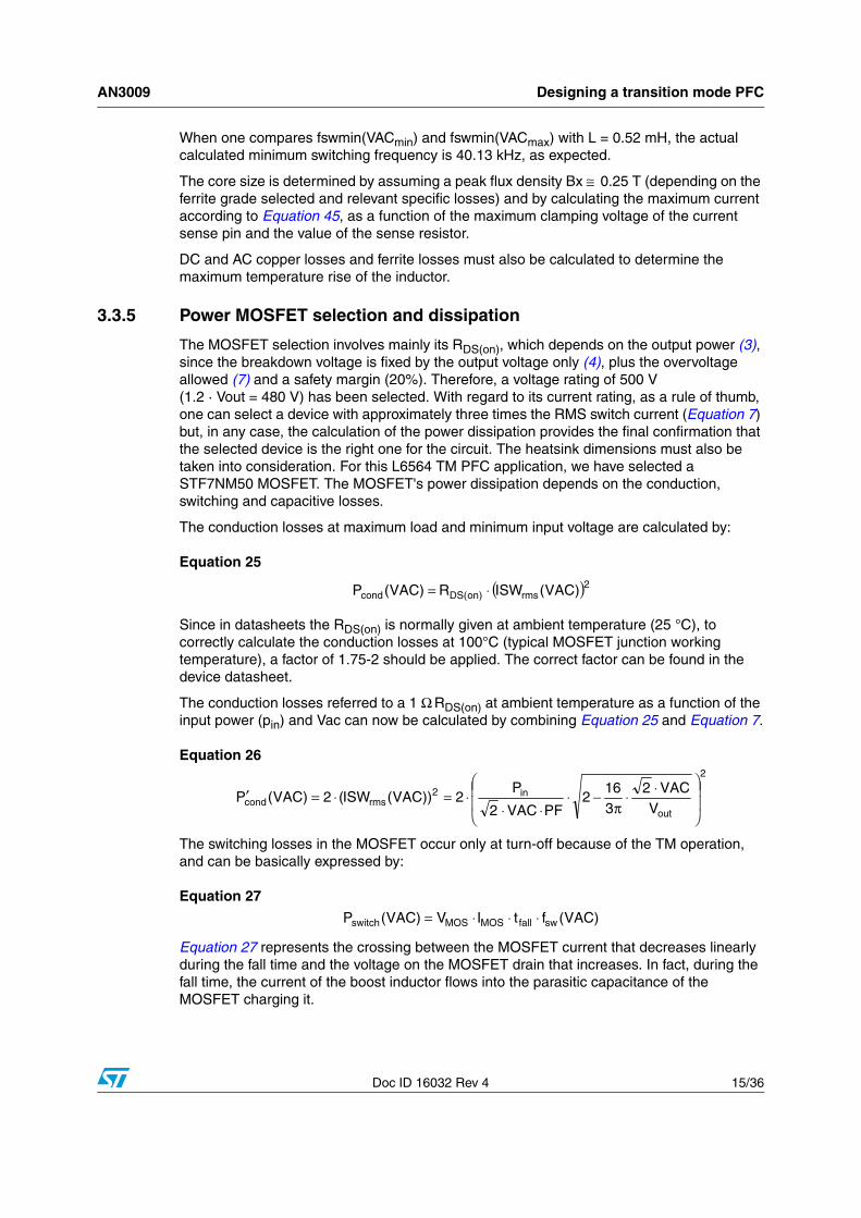
Equation 33
Figure 7 shows the trend of the total losses (derived from Equation 33) as a function of the input mains voltage for the selected MOSFET STF7NM50N. Capacitive losses are dominant at high mains voltages and are essentially caused by conduction losses at low and medium mains voltages.
Figure 5. θ1 and θ2 depending on input voltage
Figure 6. Representation of capacitive losses
)VAC(PC)VAC(PC
t)VAC(PR)VAC(P capdsw
d
2fall
cond)on(DSloss ′⋅+′⋅+′⋅=
Designing a transition mode PFC AN3009
18/36 Doc ID 16032 Rev 4
Figure 7. Conduction losses and total losses in the STF7NM50N MOSFET for the L6564 TM PFC
From Equation 33 and by using the data relevant to the selected MOSFET and calculating the losses at VACmin and VACmax, one can observe that the maximum total losses occur at VACmin. From this number and the maximum ambient temperature (12), the total maximum thermal resistance required to keep the junction temperature below 125 °C is:
Equation 34
If the result of Equation 34 is lower than the junction-to-ambient thermal resistance given in the MOSFET datasheet for the selected device package, a heatsink must be used.
The STF7NM50N junction-to-ambient thermal resistance in free-air is 62 °C/W, therefore a heatsink is necessary.
3.3.6 Boost diode selection
Following a similar criterion to the one for the MOSFET, the output rectifier can also be selected. A minimum breakdown voltage of 1.2·(Vout + ∆VOVP) and current rating higher than 3·Iout (Equation 1) can be chosen for a rough initial selection of the rectifier. The correct choice is then confirmed by the thermal calculation: if the diode junction temperature works within 125 °C, the device has been selected correctly, otherwise a bigger device must be selected.
For this 100 W application, we have selected a STTH2L06 (600 V, 2 A).
The current values of the rectifier AVG (Equation 1) and RMS (Equation 8), and the parameter Vth (rectifier threshold voltage) and Rd (dynamic resistance) given in the datasheet allow the rectifier losses to be calculated.
From the STTH2L06 datasheet the Vth is 0.89 V and Rd is 0.08 Ω.
Equation 35
)VAC(P
TC125R
loss
ambxth
−°=
WC
29W58.2
C50C125Rth
°=°−°=
rms2
doutthdiode IDRIVP ⋅+⋅= ( ) W26.0A72.008.0A25.0V89.0P 2diode =⋅Ω+⋅=
AN3009 Designing a transition mode PFC
Doc ID 16032 Rev 4 19/36
From (12) and Equation 35, the maximum thermal resistance to keep the junction temperature below 125 °C is:
Equation 36
Because the calculated Rth is higher than the STTH2L06 junction-to-ambient thermal resistance, a heatsink is not needed to properly dissipate the heat.
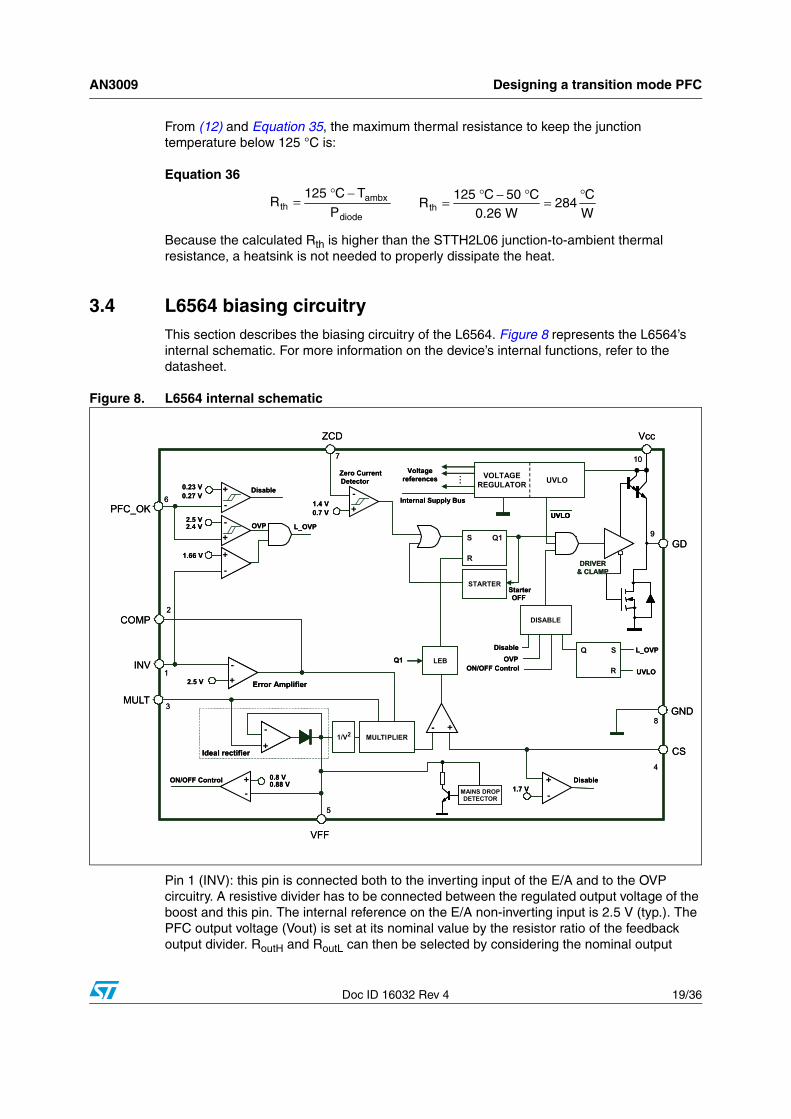
3.4 L6564 biasing circuitryThis section describes the biasing circuitry of the L6564. Figure 8 represents the L6564’s internal schematic. For more information on the device’s internal functions, refer to the datasheet.
Figure 8. L6564 internal schematic
Pin 1 (INV): this pin is connected both to the inverting input of the E/A and to the OVP circuitry. A resistive divider has to be connected between the regulated output voltage of the boost and this pin. The internal reference on the E/A non-inverting input is 2.5 V (typ.). The PFC output voltage (Vout) is set at its nominal value by the resistor ratio of the feedback output divider. RoutH and RoutL can then be selected by considering the nominal output
diode
ambxth P
TC125R
−°=
WC
284W26.0
C50C125Rth
°=°−°=

Designing a transition mode PFC AN3009
20/36 Doc ID 16032 Rev 4
voltage (4) and the desired output power dissipated on the output divider. Following is an example with a power dissipation of 50 mW.
Equation 37
mW50
)V5.2V(R
2OUT
outH−
= Ω=−= M160.3mW50
)V5.2V400(R
2
outH

AN3009 Designing a transition mode PFC
Doc ID 16032 Rev 4 21/36
By selecting a commercial value of RoutH equal to 3 MΩ, we get:
Equation 38
Equation 39
We have selected RoutL = 62 kΩ in parallel to 27 kΩ. Note that for RoutH a resistor with a suitable voltage rating (>400 V) is needed, or else additional in-series resistors must be used.
Also note that the maximum value of the resistor divider is limited by the L6564’s INV pin input bias current given in the datasheet. To guarantee correct output voltage regulation, the current flowing in the resistor divider must be significantly higher than the current flowing into the pin.
Pin 6 (PFC_OK - feedback failure protection): the PFC_OK pin is dedicated to monitoring the output voltage by a separate resistor divider. This divider is selected so that the voltage at the pin reaches 2.5 V (typ.) if the output voltage exceeds a preset value VOVP (7), usually larger than the maximum Vout that can be expected, and also including worst-case load/line transients. For a maximum output voltage VOVP of 430 V and imposing a 50 µA current flowing into the divider, we obtain:
Equation 40
By selecting a commercial value of 51 kΩ, we then get:
Equation 41
By connecting in series two 3.3 MΩ and one 2.2 MΩ resistors, a total value of 8.8 MΩ is obtained.
Note that both feedback dividers connected to the L6564’s pin #1 (INV) and pin #6 (PFC_OK) can be selected without any constraints. The unique criterion is that both dividers have to sink a current from the output bus, which needs to be significantly higher than the current biasing the error amplifier and PFC_OK comparator.
The OVP function described above can handle “normal” overvoltage conditions, that is, those resulting from an abrupt load/line change or occurring at start-up. If the overvoltage is generated by a feedback disconnection for instance, when one of the upper resistors of the output divider fails to open, an additional circuitry detects the voltage drop of pin INV. If the voltage on pin INV is lower than 1.66 V (typ.) and at same time the OVP is active, a feedback failure is assumed.
1V5.2
V
R
R out
outL
outH −= 1591V5.2V400
R
R
outL
outH =−=
159
RR outH
outL = Ω=Ω= k8.18159M3
RoutL
divider
OK_PFC_REFL I
VR = Ω=
µ= k50
A50
V5.2RL
⎟⎟⎠
⎞⎜⎜⎝
⎛−⋅= 1
V
VRR
OK_PFC_REF
OVPLH Ω=⎟⎟⎠
⎞⎜⎜⎝
⎛−⋅Ω= M721.81
V5.2V430
k51RH

Designing a transition mode PFC AN3009
22/36 Doc ID 16032 Rev 4
Thus, the activity of the gate driver is immediately stopped, the device is shut down, its quiescent consumption is reduced to less than 180 µA and the condition is latched for as long as the supply voltage of the IC remains above the UVLO threshold. To restart the system, it is necessary to recycle the input power so that the VCC voltage of the L6564 goes below 6 V and that one of the PWM controllers goes below its UVLO threshold. Note that this function offers a complete protection against not only feedback loop failures or erroneous settings, but also a failure of the protection itself. If either one of the PFC_OK dividers fails to short or open, or a PFC_OK pin is floating, the IC is shut down and the pre-regulator stopped. Moreover, the PFC_OK pin doubles its function as a not-latched IC disable: a voltage below 0.23 V shuts down the IC, reducing its consumption below 2 mA. To restart the IC, simply let the voltage at the pin go above 0.27 V.
Pin 2 (COMP): this pin is the output of the E/A that is fed into one of the two inputs of the multiplier. A feedback compensation network is placed between this pin and INV (pin #1). It has to be designed with a narrow bandwidth to prevent the system from rejecting the output voltage ripple (100 Hz) that would result in a high distortion of the input current waveform.
A simple way of defining the capacitance value is to set the bandwidth (BW) from 20 to 30 Hz. The compensation network can be a simple capacitor, providing a low-frequency pole as well as a high DC gain. A more complex network, typically a type-II CRC network providing two poles and a zero, is more suitable for constant power loads like a downstream converter.
If a single capacitor is used it can be dimensioned using the following formulas.
Equation 42
Equation 43
For a more complex compensation network calculation refer to [2] and [3] in Chapter 6: References.
For this 100 W TM PFC, a CRC network providing two poles and a zero has been implemented with the following values.
The relevant open-loop transfer function and its phase function are reported in Figure 9 and Figure 10.
(14)
( ) onCompensatioutLoutH CR//R21
BW⋅⋅π
=
( ) BWR//R21
CoutLoutH
onCompensati ⋅⋅π=
nF68CcompP = nF680CcompS = Ω= k82RcompS

AN3009 Designing a transition mode PFC
Doc ID 16032 Rev 4 23/36
The two bode plot charts refer to the PFC operating at 265 Vac and full load. In these conditions, the crossover frequency is 11.55 Hz and the phase margin is 55 °C. The third harmonic distortion introduced by the E/A 100 Hz residual ripple is below 3%.
Pin 4 (CS): this pin is the inverting input of the current sense comparator. The L6564 receives the information on the instantaneous inductor current through this pin, provided by an external sense resistor (Rs) via an RC filter. As this signal crosses the threshold set by the multiplier output, the PWM latch is reset and the power MOSFET is turned off. The MOSFET stays in the off state until the PWM latch is set again by the ZCD signal. The pin is equipped with 150 ns leading-edge blanking to improve noise immunity.
For a 100 W PFC, the sense resistor value (Rs) can be calculated as follows.
Equation 44
Where:
ILpk is the maximum peak current in the inductor, calculated as shown in Equation 4.
Vcsmin equals 1.0 V and is the minimum voltage admitted on the L6564’s current sense (as per the datasheet).
Because the internal current sense clamping sets the maximum current that can flow in the inductor, the maximum peak of the inductor current is calculated considering the maximum voltage Vcsmax admitted on the L6564 (as per the datasheet).
Equation 45
The calculated ILpkx is the value at which the boost inductor is not saturated and is used to calculate the inductor’s number of turns and air gap length.
Figure 9. Open-loop transfer function bode plot
Figure 10. Phase
pk
mins IL
VcsR < Ω=< 296.0
A38.3V0.1
Rs
s
maxpkx R
VcsIL = A30.4
27.0V16.1
ILpkx =Ω
=

Designing a transition mode PFC AN3009
24/36 Doc ID 16032 Rev 4
If the boost inductor gets saturated, a second comparison level at 1.7 V detects the abnormal current value and activates a safety procedure that temporarily stops the converter and limits the stress of the power components.
The power dissipated in Rs is given by:
Equation 46
According to the results of Equation 45 and Equation 46, two resistors of 0.47 Ω and 0.68 Ω, each with a power rating of 0.25 W, have been selected.
Pin 3 (MULT): this pin is the second multiplier input. It is connected through a resistive divider to the rectified mains to obtain a sinusoidal voltage reference. The multiplier can be described by the relationship:
Equation 47
Where:
VCS (multiplier output) is the reference for the current sense (VCS_OFFSET is its offset).
k = 0.45 (typ.) is the multiplier gain.
VCOMP is the voltage on pin #2 (E/A output).
VMULT is the voltage on pin #3.
VFF is the second input to the multiplier for 1/V2 function. It compensates the control loop gain dependence on the mains voltage. The voltage at this pin is a DC level equal to the peak voltage on the MULT pin (pin #3).
Figure 11 and Figure 12 show the typical multiplier characteristics.
2rmsss ISWRP ⋅= ( ) W37.0A18.127.0P 2
s =⋅Ω=
2FF
MULTCOMPmOFFSET_CSCS
V
V)V5.2V(kVV
⋅−⋅+=
Figure 11. Multiplier characteristics for VFF =1 V
Figure 12. Multiplier characteristics for VFF = 3 V

AN3009 Designing a transition mode PFC
Doc ID 16032 Rev 4 25/36
The linear operation of the multiplier is guaranteed within the range 0 to 3 V of VMULT and the range 0 to 1.16 V (typ.) of Vcs, while the minimum guaranteed value of the maximum slope of the characteristics family (typ.) is given in Equation 48.
Equation 48
The voltage on the MULT pin is also used to derive the information on the RMS mains voltage for the VFF compensation. The multiplier divider should be calculated by taking into account the relation with the VFF pin so that the description of the VFF pin comes before the dimensioning formula.
Pin 5 (voltage feed-forward): the power-stage gain of the PFC pre-regulators varies with the square of the RMS input voltage. So does the crossover frequency fc of the overall open-loop gain because the gain has a single pole characteristic. This leads to large trade-offs in the design. For example, setting the gain of the error amplifier to get fc = 20 Hz at 264 Vac means having an fc of about 4 Hz at 88 Vac, resulting in sluggish control dynamics. Additionally, the slow control loop causes large transient current flows during rapid line or load changes that are limited by the dynamics of the multiplier output. This limit is considered when the sense resistor is selected to let the full load power pass under the minimum line voltage conditions, with some margin. But a fixed current limit allows excessive power inputs at high lines, whereas a fixed power limit requires the current limit to vary inversely with the line voltage.
The voltage feed-forward can compensate for the gain variation with the line voltage and allow overcoming all of the above-mentioned issues. It consists of deriving a voltage proportional to the input RMS voltage, feeding this voltage into a squarer/divider circuit (1/V2 corrector) and providing the resulting signal to the multiplier that generates the current reference for the inner current control loop.
In this way, a change in the line voltage causes an inversely proportional change of the half sine amplitude at the amplifier’s output (if the line voltage doubles, the amplitude of the multiplier output is halved and vice-versa), so that the current reference is adapted to the new operating conditions with (ideally) no need for invoking the slow dynamics of the error amplifier. Additionally, the loop gain is constant throughout the input voltage range, which significantly improves dynamic behavior at low lines and simplifies loop design.
Actually, with other PFCs embedding the voltage feed-forward function, deriving a voltage proportional to the RMS line voltage implies a form of integration, which has its own time constant. If it is too small, the voltage generated is affected by a considerable amount of ripple at twice the mains frequency, which causes distortion of the current reference (resulting in high THD and poor PF); if it is too large, there is a considerable delay in setting the right amount of feed-forward, resulting in excessive overshoot and undershoot of the pre-regulator's output voltage in response to large line voltage changes. Clearly a trade-off is required.
The L6564 realizes an innovative voltage feed-forward which, with a technique that makes use of just two external parts, overcomes this time constant trade-off issue whichever voltage change occurs on the mains, both surges and drops. A capacitor CFF and a resistor RFF, both connected from the pin VFF (pin #5) to ground, complete an internal peak-holding circuit that provides a DC voltage equal to the peak of the rectified sine wave applied on the MULT pin (pin #3). In this case, the following value has been selected.
VV
66.1dV
dV
MULT
CS =

Designing a transition mode PFC AN3009
26/36 Doc ID 16032 Rev 4
In this way, if a sudden rise occurs in the line voltage, CFF is rapidly charged through the low impedance of the internal diode; if a drop occurs in the line voltage, an internal "mains drop" detector enables a low impedance switch that suddenly discharges CFF, thus avoiding a long settling time before reaching the new voltage level. Consequently, an acceptably low steady-state ripple and low current distortion can be achieved without any considerable undershoot or overshoot on the pre-regulator's output, like in systems with no feed-forward compensation. This pin is internally connected to a comparator in order to provide the brownout (AC mains undervoltage) protection. A voltage below 0.8 V shuts down (does not latch) the IC and brings its consumption to a considerably lower level. The IC restarts when the voltage at the pin goes above 0.88 V. This information has to be taken into account when the MULT divider is selected.
The procedure to properly set the operating point of the multiplier is described hereafter. First, the maximum peak value for VMULT, (VMULTmax) is selected. This value, which occurs at the maximum mains voltage, should be 3 V or nearly so in wide-range mains, and less in case of single mains. The sense resistor selected is Rs = 0.27 Ω as described in the pin #4 paragraph. According to the L6564 datasheet and the linearity setting of the pin, the maximum voltage accepted on the multiplier input is:
From (16) the maximum required divider ratio is calculated as:
Equation 49
Assuming a 60 µA current is flowing into the multiplier divider, the lower resistor value can be calculated as:
Equation 50
A commercial value of 51 kΩ for the lower resistor has been selected. The upper resistor value can now be calculated as:
Equation 51
For this application, we have selected RmultH = 6.9 MΩ and RmultL = 51 kΩ. Note that for RmultH a resistor with a suitable voltage rating (>400 V) is needed, otherwise more in-series resistors must be used.
The voltage on the multiplier pin with the selected component values is re-calculated when the minimum line voltage is 0.93 V and the maximum line voltage is 2.74 V. The multiplier works correctly within its linear region.
(15)
(16)
F1CFF µ= Ω= M1RFF
V3VMULTmax =
3
max
maxMULTp 108
Vac2652
V00.3
VAC2
Vk −⋅=
⋅=
⋅=
Ω=µ
=µ
= k50A60V00.3
A60
VR maxMULT
multL
Ω=Ω⋅
⋅−=−
= −
−M319.6k51
108
1081R
k
k1R
3
3
multLp
pmultH

AN3009 Designing a transition mode PFC
Doc ID 16032 Rev 4 27/36
Because the MULT divider also determines the mains input voltage at which the PFC starts and stops (brownout function), these values are calculated using the actual divider ratio.
Equation 52
As well as the stop voltage:
Equation 53
The start and stop PFC mains voltages are compatible with the input mains voltage range (1).
In order to obtain the required start-up and shut-down voltage, a reiteration might be required, done by selecting the MULT resistors and checking the actual PFC start and stop mains voltages.
Pin 7 (ZCD): pin #7 is the input of the zero current detector circuit. In transition mode PFC, the ZCD pin is connected through a limiting resistor to the auxiliary winding of the boost inductor. The ZCD circuit is triggered by the negative-going edge: when the voltage on the pin falls below 0.7 V, it sets the PWM latch and thus the MOSFET is turned on. However, to do so, the circuit must first be armed: prior to falling below 0.7 V, the voltage on pin #7 must experience a positive-going edge that exceeds 1.4 V (due to the MOSFET's turn-off). The maximum main-to-auxiliary winding turn ratio (nmax) must ensure that the voltage delivered to the pin during the MOSFET's OFF time is sufficient to arm the ZCD circuit. A safe margin of 15% has been added.
Equation 54
If the winding is also used to supply the IC, the above criteria may not be compatible with the VCC voltage range. To solve this incompatibility, the self-supply network shown in Figure 18 can be used.
The minimum value of the limiting resistor can be found considering the maximum voltage across the auxiliary winding with a selected turn ratio equal to 10 and assuming a 0.6 mA current through the pin.
Equation 55
Equation 56
multL
multLmultHSTART R
RR
2
V88.0V
+⋅= V4.84
k51k51M9.6
2
V88.0VSTART =
ΩΩ+Ω⋅=
multL
multLmultHSTOP R
RR
2
V80.0V
+⋅= V1.77
k51k51M9.6
2
V80.0VSTOP =
ΩΩ+Ω⋅=
15.1V4.1VAC2V
n
nmaxn maxout
auxiliary
primary
⋅⋅−
== 71.1515.1V4.1
Vac2652V400maxn =
⋅⋅−=
mA6.0
VnV
RZCDH
aux
out
1
−= Ω=
−= k16.57
mA6.0
V7.510
V400
R1
mA6.0
VnVAC2
RZCDL
aux
max
2
−⋅
= Ω=−⋅
= k4.62mA6.0
V010
Vac2652
R2

Designing a transition mode PFC AN3009
28/36 Doc ID 16032 Rev 4
VZCDH at 5.7 V and VZCDL at 0 V are the upper and lower ZCD clamp voltages of the L6564.
Considering the highest value of the two calculations, an RZCD equal to 68 kΩ has been selected as the limiting resistor.
The actual value can then be tuned by trying to make the activation of the MOSFET occur right on the valley of the drain voltage (which is resonating because the boost inductor has run out of energy – as shown in Figure 13).This minimizes the power dissipation at turn-on.
Figure 13. Optimum MOSFET activation
Pin 8 (GND): this pin acts as the current return for both the signal’s internal circuitry and for the gate drive current. When layouting the printed circuit board, these two paths should run separately.
Pin 9 (GD): this pin is the output of the driver. It can drive an external MOSFET with a 600 mA source and a 800 mA sink capability.
The high-level voltage of this pin is clamped at about 12 V so as to avoid excessive gate voltages in case the pin is supplied with a high Vcc. To avoid undesired switch-ons of the external MOSFET because of some leakage current when the supply of the L6564 is below the UVLO threshold, an internal pull-down circuit holds the pin low. The circuit guarantees 1.1 V maximum on the pin (when Isink = 2 mA), with Vcc > VCC_ON. This allows omitting the "bleeder" resistor connected between the gate and the source of the external MOSFET used for this purpose.
Pin 10 (Vcc): this pin is the supply of the device. It is externally connected to the start-up circuit (normally, one resistor is connected to the rectified mains) and to the self-supply circuit.
Whatever the configuration of the self-supply system, a capacitor must be connected between this pin and ground.
To start the L6564, the voltage must exceed the start-up threshold (12 V typ.). Below this value the device does not work and consumes less than 90 µA (typ.) from Vcc. This allows the use of high-value start-up resistors (in the hundred kΩ), which reduces power consumption and optimizes system efficiency at low loads, especially in wide-range mains applications.
When operating, the current consumption (of the device only, not of the gate drive) rises to a value that depends on the operating conditions but never exceeds 6 mA.
The device keeps on working as long as the supply voltage is over the UVLO threshold (13 V max). If the Vcc voltage exceeds 22.5 V, an internal Zener diode (rated at 20 mA) is activated in order to clamp the voltage. Remember that during normal operation, the internal

AN3009 Designing a transition mode PFC
Doc ID 16032 Rev 4 29/36
Zener does not have to clamp the voltage because the power consumption of the device increases considerably, as does its junction temperature. The suggested operating condition for safe operation of the device is below the minimum clamping voltage of the pin.

Design example using the L6564-TM PFC Excel spreadsheet AN3009
30/36 Doc ID 16032 Rev 4
4 Design example using the L6564-TM PFC Excel spreadsheet
An Excel spreadsheet is provided to allow quick and easy design of a boost PFC pre-regulator using the STM L6564 controller, operating in transition mode. Figure 14 shows the first sheet already filled with the input design data used in Chapter 3.
Figure 14. Excel spreadsheet design specification input table
Figure 15. Other design data
The tool can generate a complete parts list of the PFC schematic represented in Figure 15, including the power dissipation calculation of the main components.
∆

AN3009 Design example using the L6564-TM PFC Excel spreadsheet
Doc ID 16032 Rev 4 31/36
Figure 16. Excel spreadsheet TM PFC schematic
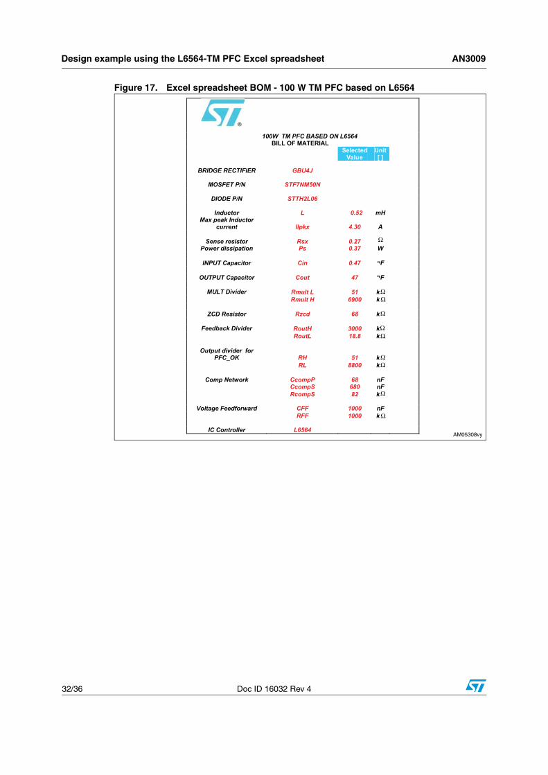
The bill of material shown in Figure 17 is automatically compiled by the Excel spreadsheet. It summarizes all the selected components as well as some salient data.
Design example using the L6564-TM PFC Excel spreadsheet AN3009
32/36 Doc ID 16032 Rev 4
Figure 17. Excel spreadsheet BOM - 100 W TM PFC based on L6564
Ω
Ω
Ω
ΩΩ
Ω
ΩΩ
Ω
¬
¬
Ω

AN3009 EVL6564-100W demonstration board
Doc ID 16032 Rev 4 33/36
5 EVL6564-100W demonstration board
Figure 18 shows the schematic of a 100 W, wide-range TM PFC based on the L6564 device. It has been dimensioned using the Excel tool presented in Chapter 4.
Figure 18. Wide-range 100 W demonstration board electrical circuit (EVL6564-100W)

References AN3009
34/36 Doc ID 16032 Rev 4
6 References
1. L6564 datasheet
2. “A systematic approach to frequency compensation of the voltage loop in boost PFC pre regulators”, abstract
3. AN1089
4. AN3022

AN3009 Revision history
Doc ID 16032 Rev 4 35/36
7 Revision history
Table 1. Document revision history
Date Revision Changes
10-Feb-2010 1 Initial release.
07-May-2010 2 Modified: Figure 10 and 15
22-Oct-2010 3 Modified: Section 3.4 and Equation 40
09-Feb-2011 4 Updated: Figure 8

AN3009
36/36 Doc ID 16032 Rev 4
Please Read Carefully:
Information in this document is provided solely in connection with ST products. STMicroelectronics NV and its subsidiaries (“ST”) reserve theright to make changes, corrections, modifications or improvements, to this document, and the products and services described herein at anytime, without notice.
All ST products are sold pursuant to ST’s terms and conditions of sale.
Purchasers are solely responsible for the choice, selection and use of the ST products and services described herein, and ST assumes noliability whatsoever relating to the choice, selection or use of the ST products and services described herein.
No license, express or implied, by estoppel or otherwise, to any intellectual property rights is granted under this document. If any part of thisdocument refers to any third party products or services it shall not be deemed a license grant by ST for the use of such third party productsor services, or any intellectual property contained therein or considered as a warranty covering the use in any manner whatsoever of suchthird party products or services or any intellectual property contained therein.
UNLESS OTHERWISE SET FORTH IN ST’S TERMS AND CONDITIONS OF SALE ST DISCLAIMS ANY EXPRESS OR IMPLIEDWARRANTY WITH RESPECT TO THE USE AND/OR SALE OF ST PRODUCTS INCLUDING WITHOUT LIMITATION IMPLIEDWARRANTIES OF MERCHANTABILITY, FITNESS FOR A PARTICULAR PURPOSE (AND THEIR EQUIVALENTS UNDER THE LAWSOF ANY JURISDICTION), OR INFRINGEMENT OF ANY PATENT, COPYRIGHT OR OTHER INTELLECTUAL PROPERTY RIGHT.
UNLESS EXPRESSLY APPROVED IN WRITING BY AN AUTHORIZED ST REPRESENTATIVE, ST PRODUCTS ARE NOTRECOMMENDED, AUTHORIZED OR WARRANTED FOR USE IN MILITARY, AIR CRAFT, SPACE, LIFE SAVING, OR LIFE SUSTAININGAPPLICATIONS, NOR IN PRODUCTS OR SYSTEMS WHERE FAILURE OR MALFUNCTION MAY RESULT IN PERSONAL INJURY,DEATH, OR SEVERE PROPERTY OR ENVIRONMENTAL DAMAGE. ST PRODUCTS WHICH ARE NOT SPECIFIED AS "AUTOMOTIVEGRADE" MAY ONLY BE USED IN AUTOMOTIVE APPLICATIONS AT USER’S OWN RISK.
Resale of ST products with provisions different from the statements and/or technical features set forth in this document shall immediately voidany warranty granted by ST for the ST product or service described herein and shall not create or extend in any manner whatsoever, anyliability of ST.
ST and the ST logo are trademarks or registered trademarks of ST in various countries.
Information in this document supersedes and replaces all information previously supplied.
The ST logo is a registered trademark of STMicroelectronics. All other names are the property of their respective owners.
© 2011 STMicroelectronics - All rights reserved
STMicroelectronics group of companies
Australia - Belgium - Brazil - Canada - China - Czech Republic - Finland - France - Germany - Hong Kong - India - Israel - Italy - Japan - Malaysia - Malta - Morocco - Philippines - Singapore - Spain - Sweden - Switzerland - United Kingdom - United States of America
www.st.com