Embed Size (px)
Citation preview
Application Note AN2118 1/11 June 2017 Rev01 www.redisem.com
AN2118 RediSem CV LED Driver Troubleshooting Overview This Quick Start Guide is a companion document to AN2117, the CV LED Design Guide and is intended to help you with troubleshooting your prototype LED driver. It assumes that your prototype is based on a standard RediSem Driver Application using the RED2541 LED CV control IC and uses the same component references for quick and easy reference. Contents Troubleshooting Steps .................................................................................................................................... 3 Start-up Problems ........................................................................................................................................... 3 Turns on, but turns off after 1-5ms .................................................................................................................. 4 Full load Regulation Problems ........................................................................................................................ 5 Instability ......................................................................................................................................................... 6 Burst threshold problems ................................................................................................................................ 7 Hot Transistors ................................................................................................................................................ 8 EMI .................................................................................................................................................................. 9 Harmonics Emissions ...................................................................................................................................... 9 Power Factor ................................................................................................................................................... 9 Fault Protection ............................................................................................................................................... 9

CV Troubleshooting
Application Note AN2118 2/11 June 2017 Rev01 www.redisem.com
Figure 1: Schematic of 60W CV LED Driver with PPFC, using RED2541

CV Troubleshooting
Application Note AN2118 3/11 June 2017 Rev01 www.redisem.com
Troubleshooting Steps Important Note: when attaching probes to the board under test, use a large common-mode choke in the line input to avoid getting misleading results and waveforms, and even damaging the circuit under test. It is best to use COM (pin 7 of the controller IC) as the scope ground reference point.
Start-up Problems VDD rail stuck low Check the VDD pin for a sawtooth waveform (Figure 2) – this shows that the IC (RED2541) is attempting to start up. If the VDD rail is stuck below 3.3V and there is no sawtooth, check:
D18 damaged or wrong way round R18 or R19 value too low (remove them temporarily) R7, R8, R11, R14, R26, R27, R28 values too high C13, C15 or C17 leaky U3 (optocoupler) damaged RED2541 inserted the correct way around
No drive pulses If the VDD sawtooth looks OK, next check TX1, TX2 pins on IC (RED2541) for drive pulses (Figure 3). If no pulses present, check:
R15, R41 open-circuit RED2541 pin 2 (NTC input) shorted to GND L4 too small (remove temporarily)
BJTs not commutating If there are drive pulses on TX1, TX2, check the Mid-Point node (junction of Q1 emitter and Q2 collector) for commutation (use HT- as the scope reference point). See Figure 4. If no commutation, possible faults include:
T1 windings incorrect R3, R4 damaged Q1, Q2 damaged RED2541 pin 8 (CS input) open-circuit C9, C7 too big Open-circuit fault in primary current loop
No output If the BJTs are commutating, check the output terminals for sign of short-circuit fault (disconnect line and load terminals first). A short-circuit can be caused by a faulty output diode (D20) or reversed output capacitor C11. If no short-circuit is found, check:
T2 secondary windings phasing D20 output diodes
Figure 2: VDD (repeated re-start attempts)
Figure 3: Tx pin drive pulse
Figure 4: mid-point commutation

CV Troubleshooting
Application Note AN2118 4/11 June 2017 Rev01 www.redisem.com
Turns on, but turns off after 1-5ms Foldback Protection The RED2541 includes a foldback protection to abandon startup if an abnormal load condition is detected. In foldback, the current limit is set to 50% until the output voltage reaches 30%. It is best to configure the E-load in constant resistance (CR) mode. However, if you have to test with an E-load in Constant Current (CC) mode, you must configure it to be inactive while the output voltage is below 30%. Normal loads must comply with the characteristics shown in Figure 5. Suitable loads include the following:
- LED, CR (constant resistance) and CV (constant voltage); - CC (constant current) and CP (constant power) – load must be inactive when VLOAD < 30% VNOM.
[Special note for CP loads and high capacitance loads: if the load requires a large current to pull it up, increase the value of R45 (maximum permitted value is 130) but beware of higher peak currents in the primary loop causing problems – inductor saturation, etc]
VDD Supply drops out Check VDD and primary current during start up (Figure 6). If VDD drops below 2.4V during the start-up, the IC will stop and re-start. Possible causes are:
C18 too small C11 (or load capacitance) too large Current Limit too low T2 aux winding too few turns R10 value too large D18 faulty/missing R18 value incorrect Secondary regulation error R16, R41 missing C12 s/c fault
If the load requires a large current to pull it up, increase the value of R45 (maximum permitted value is 130) but beware of higher peak currents in the primary loop causing problems – inductor saturation etc.
V(LOAD) i(LOAD)
30% 100%
50%
100%
0%
Figure 6: VDD, primary current (good startup)
Figure 5: Static characteristics of allowed loads
Capable Load Range

CV Troubleshooting
Application Note AN2118 5/11 June 2017 Rev01 www.redisem.com
VFB Low Fault If VDD looks OK during startup, check RED2541 pin 1 (VFB input) during startup (Figure 7). If the VFB pin voltage has not risen above 300mV after 128 cycles (about 3ms), the controller registers a fault, shuts down and attempts to re-start. If this occurs, check:
R18 missing or incorrect size R41 missing T2 aux winding too few turns
Full load Regulation Problems If the converter cannot maintain the output at full load, reduce the load until it can regulate, then perform the following checks: Oscillator error Monitor RED2541 pin 5 (RC input) waveform (Figure 8) through a line cycle. Check that the highest waveform peaks are less than 2.2V at full load. If not, check:
C42 value R7, R8, R11, R14 values
Current sensing error Check:
Value of R5, R6 (current sense resistors) Values of C7, C26, R9 (parallel current compensation) Phase of Aux winding on T2 – change the direction if in doubt
Base Drive error If the inductance seen across the control winding of T1 is too small, this will limit the frequency range, reducing the maximum output power. Check:
T1, L4 inductance values (remove L4 briefly to check) T1 turns ratio
Figure 7: VFB pin during startup
Figure 8: RC pin at full load
Opto turns on
3ms
CV Troubleshooting
Application Note AN2118 6/11 June 2017 Rev01 www.redisem.com
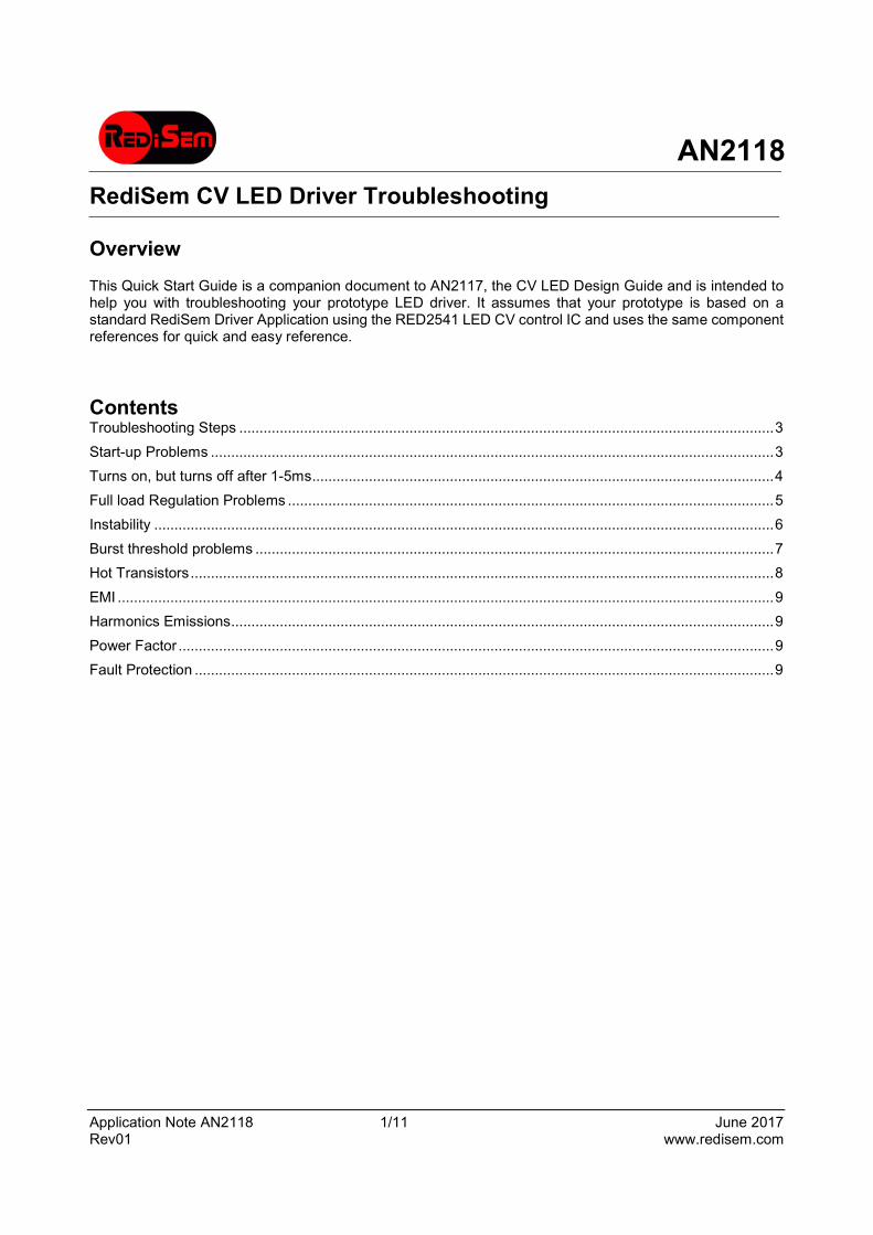
Capacitive mode protection error Monitor the waveforms of primary current and RED2541 pin 5 (RC), checking for capacitive mode limiting. A good design should hit the capacitive limit at full load when line input is <198Vac. (Figure 10, Figure 9). If capacitive mode limiting occurs within the target line/load range, check:
T2 transformer turns ratio R5 value Boost capacitor values
Secondary voltage regulation error If the output appears to be regulating too low, temporarily short out U3 pins 1,2 (optocoupler inputs). If the output rises, it shows the problem is in the secondary voltage sensing circuit. Check:
R35, R36, R37 values R38 value too high
High Output Ripple Check the feedback loop values are all correct or similar to the suggested values. Check that there are no primary side regulation errors by increasing the value of R18. High leakage in the transformer can cause high spikes on the aux winding of T2. This is especially worse on low voltage high current designs Primary voltage limiting error Run the driver with nominal line, full load and temporarily short out the optocoupler LED (U3 pins 1,2). The output voltage should rise to 105-110% of the nominal output voltage. If not, adjust the value of R18 (decrease R18 to decrease output voltage). Other things to check:
Noise on VFB pin (because C12 missing or too small) T2 – aux winding - too many turns? T2 leakage inductance – aux winding should be outermost (ie on top of the secondary windings)
Instability Unstable at normal loads Check primary current waveform for signs of instability across full range of line inputs, and load range 10%-100%. If system is unstable at nominal line voltage check:
C40 (increase value for more stability) C11, R35 (time constant should be ~50usec) C12, R41 (time constant should be ~20usec) R39 (increase value for more stability) R42 (too large?) U3 (optocoupler) gain factor
Figure 10: Primary current and RC pin on edge of capacitive mode switching
Figure 9: Primary current and RC pin on edge of capacitive mode switching (zoomed in)

CV Troubleshooting
Application Note AN2118 7/11 June 2017 Rev01 www.redisem.com
The values given in the reference design assume a typical low-cost optocoupler (e.g. PC817 grade B), with CTR < 260%. If the maximum CTR > 260%, consider increasing R39 value for stability. Decrease R39 for higher loop gain, lower output ripple. If system is unstable only at low line voltage, check:
T2 turns ratio T1 turns ratio T1, L4 inductance values (remove L4 briefly to check)
Unstable at low loads Burst threshold may be too high, refer to “Burst threshold problems” section below. Unstable in standby Check output voltage waveform for signs of instability in standby by stepping load from 10% and 0%. Some overshoot and undershoot is acceptable, see Figure 11. But, if instability is present, check:
C40 value (too small?) C17 value (too small?) R10 value (too large?) R38 value (too large?)
Burst threshold problems The burst threshold should normally be in the load range 5-10%. Burst threshold too high If bursting occurs with loads > 10%, increase the load until it does run continuously then perform the following checks. Oscillator error Monitor RED2541 pin 5 (RC) waveform (Figure 12) through a line cycle. The controller IC will enter burst mode if the maximum frequency limit is reached, i.e. when the peaks of the RC waveform are <350mV. Check that the lowest waveform peaks are >400mV. If not, check (decrease):
C42 value R7, R8, R11, R14 values
Figure 11: output voltage with load steps 0-10%
Figure 12: RC pin at 10% load
CV Troubleshooting
Application Note AN2118 8/11 June 2017 Rev01 www.redisem.com
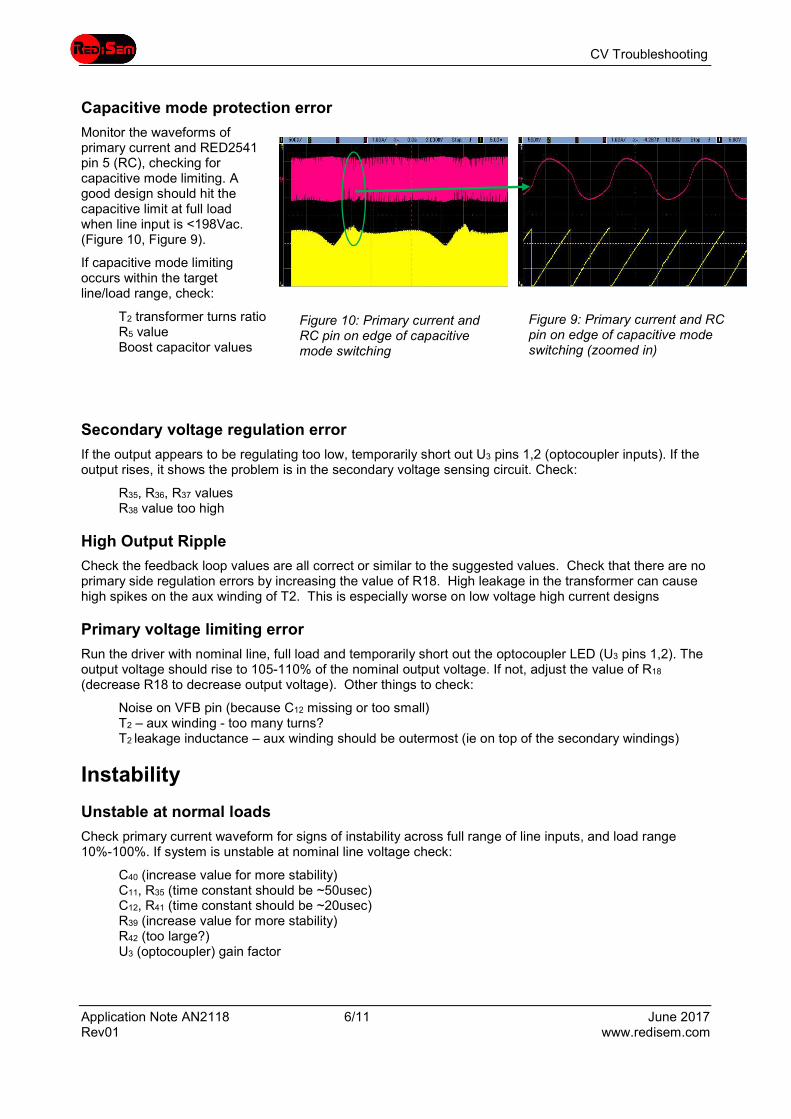
Load current correction error Connect a scope probe (as close as possible) to RED2541 pin 8 (CS) and compare the waveform to the yellow trace in Figure 13 (some ringing is acceptable). If the flat parts of the waveform are very different to those shown, check:
R9, R29 values C7, C26 values T2 construction - aux winding reversed or incorrect turns?
If the ringing is severe, check:
T2 construction details – aux winding should be on outside of secondary windings T2 construction details – secondary windings leadouts must be short
Burst threshold too low In no-load condition, if the driver does not enter burst mode, there is a problem with the load current correction - see section above.
Hot Transistors Conduction Losses Using a voltage-clamped scope probe amplifier (or equivalent) measure the on-state voltage. Check that the on-state voltage of both transistors is <300mV. If the on-state is higher than this, possible causes include:
Q1, Q2 current rating or hFE too small Base drive transformer T1 turns ratio too large
Switching Losses Check the storage and fall times of both transistors using scope probes to monitor the base-emitter and collector-emitter waveforms. At minimum line voltage and maximum load, the storage time (tS) should be roughly 200ns and the fall time (tF) should be <200ns. If this is not the case, possible causes include:
Q1, Q2 too slow R3, R4 values too small T1 inductance too high C9 too small
Shoot-through Monitor the collector current of Q1 (or Q2) using a current transformer. If there are any sharp current spikes in the waveform, please check:
Base Drive transformer T1 construction – windings bunched incorrectly Flywheel diodes D14, D15 turn-on too slow C9 wrong side of T1 primary winding
The ceramic capacitors C20, C21 between base and emitter of Q1 and Q2 help to suppress shoot-through.
Figure 13: Primary current and CS pin waveforms

CV Troubleshooting
Application Note AN2118 9/11 June 2017 Rev01 www.redisem.com
EMI Conducted Emissions 50k – 500kHz Differential-mode: Increase C1, C2 and L1 (Note: increasing C1, C2 will reduce PF) Common-mode: Make sure that the transformer construction (order and phasing of windings) is correct. A screen winding should not be necessary, but can help if all else fails. Minimise lengths of secondary winding leadouts. Increase common-mode choke L3 or the Y-Capacitor C32. Check PCB tracking. Make sure that the noisy midpoint node is not close to the secondary or mains input. 2MHz – 30MHz Minimise lengths of PCB tracks associated with base drive transformer T1. Radiated Emissions 30 - 100MHz Minimise the tracking around the T1 base drive transformer. Test to see if one of the diodes D14, D15 is causing ringing. Add 10R in series with aux diode D18. Divide the midpoint capacitor C9 into two and place directly across the freewheel diodes D14 and D15
Harmonics Emissions Non-compliant at low line, high load Boost voltage too high
C3, C5 values too small C4, C6, C8 values too large
Non-compliant at high line, low load Boost voltage too low
C3, C5 values too large C1, C4, C6, C8 values too small
Power Factor As for Harmonics Emissions above, plus:
C1, C2 values too large – Increase the size of the Inductor to maintain EMI compliance
Fault Protection Short-circuit load – Bulk Supply Voltage too high (PPFC apps only)
T2 aux winding turns ratio T2 construction – Aux winding should be outside the secondary windings
Optocoupler fault - output voltage too high R18 too large Voltage control loop unstable (see above) C9 too large

CV Troubleshooting
Application Note AN2118 10/11 June 2017 Rev01 www.redisem.com
T1 or L4 inductance too large Capacitive Mode happens at normal line voltages
T2 turns ratio too low C9 value too large
Fault Recovery Time Too short:
Increase C17, C18 Increase R7, R11, R14 (adjust C13 to keep same clock setting) (adjust R19 to keep same minimum line voltage for startup)
Too long: Decrease C17, C18 Decrease R7, R11, R14 (adjust C13 to keep same clock setting) (adjust R19 to keep same minimum line voltage for startup)
CV Troubleshooting
Application Note AN2118 11/11 June 2017 Rev01 www.redisem.com
About RediSem RediSem designs and supplies semiconductor ICs for energy efficient power management applications. RediSem uniquely combines extensive experience in power electronics with in-depth knowledge of IC design and manufacturing and works with the world’s top suppliers and customers. RediSem’s unique patented IC and converter technologies deliver maximum efficiency and performance, while reducing overall bill of materials cost through the use of bipolar transistors. RediSem’s range of LED control ICs can be used with RediSem’s patented single stage LED control solution to provide very high efficiencies with low EMI – all with a single IC. When combined, these features deliver a low cost, high performance LED driver solution. RediSem’s fluorescent driver controller ICs achieve the advanced performance of MOSFET drivers by using bipolar transistors at a fraction of the BOM cost. RediSem’s range of SMPS (Switched Mode Power Supply) control ICs enables low-cost LLC converters with bipolar transistors that deliver very high efficiencies already meeting DoE Level VI regulations, have low standby power and have much lower EMI compared to flyback converters. All RediSem ICs are supported by comprehensive turn-key application designs enabling rapid time to market. For further information please use our contact details below Contact Details RediSem Ltd. 301-302 IC Development Centre No 6 Science Park West Avenue Hong Kong Science & Technology Park Shatin, New Territories Hong Kong Tel. +852 2607 4141 Fax. +852 2607 4140 Email: [email protected] Web: www.redisem.com Disclaimer The product information provided herein is believed to be accurate and is provided on an “as is” basis. RediSem Ltd assumes no responsibility or liability for the direct or indirect consequences of use of the information in respect of any infringement of patents or other rights of third parties. RediSem Ltd does not grant any licence under its patent or intellectual property rights or the rights of other parties. Any application circuits described herein are for illustrative purposes only. Specifications are subject to change without notice. In respect of any application of the product described herein RediSem Ltd expressly disclaims all warranties of any kind, whether express or implied, including, but not limited to, the implied warranties of merchantability, fitness for a particular purpose and non-infringement of third party rights. No advice or information, whether oral or written, obtained from RediSem Ltd shall create any warranty of any kind. RediSem Ltd shall not be liable for any direct, indirect, incidental, special, consequential or exemplary damages, howsoever caused including but not limited to, damages for loss of profits, goodwill, use, data or other intangible losses. The products and circuits described herein are subject to the usage conditions and end application exclusions as outlined in RediSem Ltd Terms and Conditions of Sale. RediSem Ltd reserves the right to change specifications without notice. To obtain the most current product information available visit www.redisem.com or contact us at the address shown above.


![10EDI2020-21-FBR Wet Riser Recall3 · 2020. 7. 31. · 1dph ri :run 7urxeohvkrrwlqj ri zhw ulvhu v\vwhp lq 7( )orzhu %d]ddu &khqqdl 5hfdoo ,qwhuqhw grzqordghg frs\ &rqwudfwru 3djh](https://img.dokumen.tips/doc/110x75/60e6bdedf2a9e9418534d17b/10edi2020-21-fbr-wet-riser-2020-7-31-1dph-ri-run-7urxeohvkrrwlqj-ri-zhw-ulvhu.jpg)


![Cinema 1, the Movement-Image by Gilles Deleuze; Hugh ... · 'lvfrxuvh flqhpdwlf dssdudwxv wxuqv vkrw iudplqj prqwdjh wkh xvh ri vrxqg dqg froru dqg doo wkh uhvw +rzhyhu 'hohx]h v](https://img.dokumen.tips/doc/110x75/5ae8cc5f7f8b9a08779036b7/cinema-1-the-movement-image-by-gilles-deleuze-hugh-lvfrxuvh-flqhpdwlf-dssdudwxv.jpg)

![VWHPV 'HVLJQ 7URXEOHVKRRWLQJ 6ROXWLRQV · 2017-05-09 · ì î l ì ñ l î ì í ó ï Á Á Á X P o } o ] v l i Ç u X } u ' o } o / v l i ^ Ç u > )ORZ 0RGHV W íW íW î í X](https://img.dokumen.tips/doc/110x75/5f05feab7e708231d415c3a8/vwhpv-hvljq-7urxeohvkrrwlqj-2017-05-09-l-l-.jpg)


