Embed Size (px)
Citation preview

© Freescale Semiconductor, Inc., 2005. All rights reserved.
Freescale SemiconductorApplication Note
AN1902Rev. 3.0, 12/2005
1.0 PurposeThis document provides guidelines for Printed Circuit Board (PCB) design and assembly. Package performance such as: MSL rating, board level reliability, electrical parasitic and thermal resistance data are included as reference.
2.0 ScopeThe Application Note is written generically to encompass various Quad Flat Pack No-lead (QFN) packages assembled internally and externally. It should be noted that device specific information is not provided. This document serves only as a guideline to help develop a user specific solution. Actual experience and development efforts are still required to optimize the process per individual device requirements and practices.
The document combines information from two separate studies. This is the first data consolidation attempt. When recommendation varies between the two studies, both views are provided and the source noted.
Quad Flat Pack No-Lead (QFN)
Contents 1.0 Purpose . . . . . . . . . . . . . . . . . . . . . . . . . . . . . . . .1
2.0 Scope . . . . . . . . . . . . . . . . . . . . . . . . . . . . . . . . . .1
3.0 Quad Flat Pack No-Lead (QFN) Package . . . . .2 3.1 Package Description. . . . . . . . . . . . . . . . . . . . . .2 3.2 Package Dimensioning. . . . . . . . . . . . . . . . . . . .2 3.3 QFN Package Design . . . . . . . . . . . . . . . . . . . . .2 3.4 Process Flow . . . . . . . . . . . . . . . . . . . . . . . . . . . .4
4.0 Printed Circuit Board (PCB) Level Guidelines .5 4.1 PCB Design Guideline . . . . . . . . . . . . . . . . . . . .5 4.2 Stencil Design Guideline . . . . . . . . . . . . . . . . .10
5.0 PCB Assembly. . . . . . . . . . . . . . . . . . . . . . . . . .14 5.1 Assembly Process Flow . . . . . . . . . . . . . . . . . .14 5.2 QFN Assembly Guideline . . . . . . . . . . . . . . . . .14 5.3 Rework Procedure . . . . . . . . . . . . . . . . . . . . . .19
6.0 Moisture Sensitivity Level Rating . . . . . . . . . .21
7.0 Board Level Reliability . . . . . . . . . . . . . . . . . . .21 7.1 Testing Details. . . . . . . . . . . . . . . . . . . . . . . . . .21 7.2 Solder Joint Reliability (SJR) Results . . . . . . .22 7.3 Increasing SJR for High Reliability
Applications . . . . . . . . . . . . . . . . . . . . . . . . . . . .24
8.0 Package Thermal Resistances. . . . . . . . . . . . .24
9.0 Electrical Performance . . . . . . . . . . . . . . . . . . .26
10.0 Reference. . . . . . . . . . . . . . . . . . . . . . . . . . . . . .30

Quad Flat Pack No-Lead (QFN), Rev. 3.02 Freescale Semiconductor
Quad Flat Pack No-Lead (QFN) Package
3.0 Quad Flat Pack No-Lead (QFN) Package
3.1 Package DescriptionThe QFN package is a lead-less, near Chip Scale Package (CSP) with low profile (1.0 mm and less), moderate thermal dissipation and good electrical performance. QFN is a surface mount plastic package with leads located at the bottom of the package. A thermally enhanced QFN with an exposed die pad is available and is denoted as QFN-EP. The suffix �EP� stands for exposed pad. EIAJ and JEDEC have their respective design guideline and structure description for this package. Freescale adopted the QFN-EP package design rule under JEDEC, document MO-220 [1].
Figure 1. QFN and QFN-EP Packages from Freescale SPS
3.2 Package DimensioningAvailable QFN packages range from 3.0 x 3.0 mm to 9.0 x 9.0 mm in size. As the package size shrinks and the lead count increases, the dimension tolerance and positioning accuracy affect subsequent processes. Special care must be taken when preparing for test, especially in the test contactor cavity design and contactor pin location. Further down the process, the PCB layout and stencil designs are critical to ensure sufficient solder coverage between the package and the Printed Circuit Board (PCB). When designing the PCB layout, refer to the Freescale case outline drawing to obtain the package dimensions and tolerances.
Part interchangeability is a concern when primary and secondary QFN suppliers both provide production parts. The optimized PCB layout of primary supplier may have issues (manufacturing yield and/or solder joint life) with the secondary supplier, especially when two styles of the QFN packages are selected (See Section 3.3). When more than one QFN source is expected, the PCB layout should be designed for robustness. Additional information of this topic is provided in the PCB Design Guidelines section.
3.3 QFN Package Design
3.3.1 Cross SectionA typical QFN cross section, depicted in Figure 2, illustrates a leadframe based package with wirebonding technology. The die is usually epoxy attached to die pad (or flag) with an option for the die pad exposure (QFN-EP version) external to the package. This option is denoted as

Quad Flat Pack No-Lead (QFN), Rev. 3.0Freescale Semiconductor 3
Quad Flat Pack No-Lead (QFN) Package
�optional exposed heat sink� in Figure 2. In most cases, gold wire is used in wirebonding, ranging anywhere from 1.0 mil to 2.0 mils.
Figure 2. General QFN Cross Section
3.3.2 Singulation MethodThe main difference in QFN package design is the singulation method. The individually molded style is called punch singulated QFN, whereas the Molded Array Package (MAP) style is sawn, similar to wafer sawing. In this section both styles of QFN are discussed. In subsequent sections, guidelines or information related to a specific style of QFN is stated as such; otherwise the material applies to both QFN styles.
3.3.2.1 MAP QFN: “E” Style
The MAP style QFN package has two types of lead terminal features. The �E� version follows JEDEC MO-220 design guideline. The lead extends to the package perimeter, where the lead ends are fully exposed to the side of the package (see Figure 3). A solder fillet is expected to form and should be visible on the PCB after the solder reflow process.
Figure 3. MAP QFN "E" Version [2]: Left-Bottom View, Right-Tilted to Show Side and Bottom Views
MAP-Style Saw Singulated Body or Individually Molded Body With Punch Press Excision
Epoxy Die Attach Gold Wire
Optional exposed heat-sinkSolderable Lead Frame & Heat Sink with Locking Features
Typical QFN Cross-Section

Quad Flat Pack No-Lead (QFN), Rev. 3.04 Freescale Semiconductor
Quad Flat Pack No-Lead (QFN) Package
3.3.2.2 MAP QFN: “S” Style
The �S� style is a Freescale version based on JEDEC MO-220 with an exception in the lead end feature. The lead end is slightly recessed from the package perimeter due to a ½ etched leadframe. No solder fillet is expected after the solder reflow process (see Figure 4).
Figure 4. MAP QFN "S" Version [2]: Left-Bottom View, Right-Tilted to Show Side and Bottom Views
3.3.3 Punch Singulated QFNThe punch singulated QFN is also a JEDEC compliant design. The bottom lead portion of the package protrudes outwards compared to the top portion, leaving a ledge for the solder fillet (see Figure 5).
Figure 5. Punch Singulated QFN [3]
3.4 Process Flow
3.4.1 QFN Package Process FlowThe MAP style QFN package process flow is illustrated in Figure 6. The illustration displays the difference between the Quad Flat Pack (QFP) and QFN process flows. The QFN package process flow is dependent upon the material set and factory. The Freescale MAP style QFN is assembled using pre-plated NiPdAu leadframes and does not require any post plating process. For the punch singulated QFN process, the tape and de-taping operations displayed in Figure 6 are not required.

Quad Flat Pack No-Lead (QFN), Rev. 3.0Freescale Semiconductor 5
Printed Circuit Board (PCB) Level Guidelines
Figure 6. Freescale MAP Style QFN Process Flow
4.0 Printed Circuit Board (PCB) Level Guidelines
4.1 PCB Design GuidelineThe PCB design guidelines are separated in two sections: Freescale MAP QFN Specific Guidelines and Robust Design Guideline. Two separate Freescale sites evaluated the QFN package. One concentrating on MAP style QFN and the other using both MAP and punch singulated QFN package styles. As explained in the Package Dimensioning section, part interchangeability becomes important with multiple QFN suppliers. The Robust Design Guideline section may not be optimal for one specific QFN supplier, but it takes into consideration both MAP and non-MAP QFN styles with good manufacturing yield and solder joint reliability.
4.1.1 Freescale MAP QFN Specific Guidelines [2]
4.1.1.1 Perimeter Pad Design Guidelines
The perimeter pad guideline specific to Freescale MAP style QFN is provided in this section. Since it is harder to prevent solder bridging in smaller pitch packages, the evaluation was performed using 0.5 mm pitch MAP QFN. There are two approaches in PCB pad designs, namely Non-Solder Mask Defined Pad (NSMD) and Solder Masked Defined Pad (SMD).
The NSMD has an opening that is larger than the copper pad. The PCB pad area is controlled by the size of the copper pad. Since the copper pad etching process is rather capable and stable, smaller size copper pad can be defined accurately. As QFN is a fine pitch and small outline package, it is recommended to use the NSMD method to define the perimeter pad on the PCB. The clearance around the copper pad and solder mask should be 75 µm nominal to account for the registration tolerance of the solder mask.

Quad Flat Pack No-Lead (QFN), Rev. 3.06 Freescale Semiconductor
Printed Circuit Board (PCB) Level Guidelines
Figure 7. NSMD Design on MAP QFN Lead/Terminal
4.1.1.2 PCB Thermal Pad Guidelines
The QFN package, with its exposed die pad soldered to the PCB, has a good thermal path to the board. The thermal performance of the package is greatly influenced by the PCB design. The PCB thermal pad should be Solder Mask Defined (SMD). The pad area is controlled by the size of the solder mask opening. The size of the thermal pad land pattern should be equal to the exposed pad of the QFN. Finally, the solder mask opening should overlap the edges of the PCB thermal pad land by at least 65 µm on all four sides.
Figure 8. SMD Design on QFN Thermal Pad
4.1.1.3 Spacing Between Lead and Thermal Pad
The design of the pattern and the size of the thermal pad depend heavily on the thermal characteristic and power dissipation of the specific product. In general, the size of the thermal pad should be as close to the exposed pad of the package as possible, provided that there is no bridging between the thermal pad and the perimeter lead pads. In the evaluation, the size of the thermal pad was kept constant to the exposed pad and no bridging was found in all samples. The thermal pad size, therefore, can be the size of the exposed pad in 4 x 4 mm and 9 x 9 mm QFN.
75µm75µm75 µm 75 µm
≥0.065mm≥0.065mm≥0.065 mm ≥0.065 mm

Quad Flat Pack No-Lead (QFN), Rev. 3.0Freescale Semiconductor 7
Printed Circuit Board (PCB) Level Guidelines
4.1.1.4 PCB Requirement
The specification of the PCB used in this study is summarized in Table 1.
4.1.1.5 Land Pattern Figure and Dimension
The land pattern and dimension recommendations are provided in Figure 9 and Table 2.
Figure 9. Land Pattern
Table 1. PCB Specification
PCB Material FR4
PCB Size 4″ x 4″
PCB Thickness 1.0 mm
Plating Flash Gold
Plating Thickness 0.05 µm � 0.127 µm
Solder Mask Non-Solder Mask Defined Pad on Perimeter Lead. Solder Mask Defined Pad on Thermal Pad.
Table 2. Land Dimensions
4 x 4 9 x 9
Version E S E S
Number of pins 16 16 64 64
A - Pitch (mm) 0.65 0.65 0.5 0.5
B - Lead pad length (mm) 0.92 0.92 0.69 0.69
C - Lead pad width (mm) 0.37 0.37 0.28 0.28
D1 - Thermal pad width (mm) 2.0 2.0 7.1 7.1
D2 - Thermal pad length (mm) 2.0 2.0 7.1 7.1
Maximum component lead length (mm) 0.75 0.75 0.5 0.5
Maximum component lead width (mm) 0.37 0.37 0.3 0.3
B
C
D1
D2
D1
A
D2
C
B

Quad Flat Pack No-Lead (QFN), Rev. 3.08 Freescale Semiconductor
Printed Circuit Board (PCB) Level Guidelines
The PCB terminal pad should be approximately 0.05 mm longer than the length of the package lead. The extra 0.05 mm should extend towards the center of the package. This provides a slack to accommodate the placement tolerance of the component during the pick & place process. Details of the land design for 4 x 4 mm and 9 x 9 mm QFN are shown in Figure 10.
Figure 10. (L) QFN 4 x 4, (R) QFN 9 x 9 mm Land Pattern Design
Notes: 1. Since the lead pitch of 9 x 9 mm QFN is much finer than the 4 x 4 mm QFN, the land pad width for 9 x 9 mm is designed to be
0.02 mm less than the maximum lead width so as to avoid bridging between adjacent leads.2. In this evaluation, the same land pattern design and process parameters were used for both �S� and �E� styles. Since there
was no adverse result after the soldering process (before and after the solder joint continuity test), it is believed that the PCB land design is appropriate.
3. For other QFNs with pitch and lead dimension different from the styles used in this study, further evaluation is required to determine the optimal design.
4.1.2 Robust Design Guidelines
4.1.2.1 Perimeter Pad Design Guidelines
The two main PCB perimeter pad design factors are the pad (terminal) length and the spacing between pads (depicted as edge-to-edge spacing in Figure 11). Table 3 provides a summary of package pad width and spacing between package pads from the case outline drawings.
The 0.20 mm package pad edge-to-edge spacing (for maximum pad width limit) can be challenging in the PCB layout. The PCB pad width can be designed smaller than the maximum possible package pad width dimension to allow for greater assembly process window. More common in the industry would be to use a 1:1 ratio between the nominal package pad width and
Table 3. Case Outline Dimensions for QFN Package Pad Width
Case Outline Pad Width Limits
0.50 mm Pitch QFN Pad Spacing 0.65 mm
Pitch QFN Pad Spacing
Minimum 0.18 mm 0.32 mm 0.23 mm 0.42 mm
Nominal (Center) 0.24 mm 0.26 mm 0.30 mm 0.35 mm
Maximum 0.30 mm 0.20 mm 0.37 mm 0.28 mm
0.05 mm
0.92 mm
0.37 mm
Component lead
0.05 mm
0.69 mm
0.28 mm
PCB land

Quad Flat Pack No-Lead (QFN), Rev. 3.0Freescale Semiconductor 9
Printed Circuit Board (PCB) Level Guidelines
the PCB pad width. In this case, the 0.50 mm pitch QFN package has a package pad edge-to-edge spacing of 0.26 mm, which is more easily manufactured.
Figure 11. PCB Pad Dimensions
The concern shifts from shorting between neighboring perimeter pads to pad-to-exposed pad (die attach paddle) shorting. The larger the spacing between the PCB perimeter pads and exposed pad, the less likely for solder shorts due to tolerance stacking. Table 4 provides pad-to-exposed pad spacing for various QFN packages. For assembly, the PCB EP should be smaller than the nominal package QFN so that at least 0.250 mm of space between input/output (I/O) leads and the EP edge exists.
For general guidelines, the PCB pad should be long enough to accommodate the largest package pad. The PCB pad should extend past the exterior package edge for the solder fillet to form. Freescale recommends this value to be approximately 0.15 mm (external to the package).
4.1.2.2 PCB Thermal Pad Guidelines
The exposed pad (EP) on many QFN packages dissipates heat from the actual device. The thermal path between the package and the PCB is important for the long term survival of the device. The PCB EP area will be slightly smaller than the package EP. The PCB EP is still a large solderable area. The stencil opening for the EP region should be segmented in several smaller areas (as explained in Section 4.2). The PCB EP region itself can also be segmented, matching the stencil pattern. If this is the case, the spacing between segments should be 0.15 mm or more.
Table 4. Spacing Between Maximum Package Pad and Maximum Exposed Pad
QFN Package Maximum Pad MaximumExposed Pad
Spacing inbetween
32 QFN 0.50 mm 0.50 mm 3.25 mm 0.37 mm
32 QFN 0.65 mm 0.75 mm 4.85 mm 0.32 mm
48 QFN 0.50 mm 0.50 mm 6.25 mm 0.37 mm
44 QFN 0.65 mm 0.75 mm 6.85 mm 0.32 mm
Package Pitch
Length
WidthEdge-to-Edge
Spacing

Quad Flat Pack No-Lead (QFN), Rev. 3.010 Freescale Semiconductor
Printed Circuit Board (PCB) Level Guidelines
4.1.2.3 Solder Mask Opening for PCB Area
The solder mask opening around the PCB pads can be as large as the spacing between pads (see Figure 12). The area in between the pads may be too thin for solder mask and the solder mask can lift off from the PCB. A potential solution is not to solder mask along the pad-to-pad spacing and only have the �toes� of the pads covered with solder mask for better PCB strength.
Figure 12. Pad and Solder Mask with Thin Webbing
4.1.3 Plated Through Hole (PTH) Vias The Plated Through Hole (PTH) recommendation applies to both Freescale MAP QFN and Robust Design sections. PTH vias, or more commonly known as via holes, increase the thermal conduction through dielectric layers. PTH vias connect the PCB thermal pad to any electrically appropriate internal PCB plane(s). Although the customer should use a maximum number of PTH vias, they impact the soldering surface of the PCB thermal pad. PTH vias should be plugged with epoxy or tented with solder mask to avoid low package stand-off height due to solder wicking into the PTH vias during the reflow process. For double sided PCB, the untented PTH vias has the potential for solder to reach the PCB top side and cause secondary reflow, leading to potential opens and shorts. A recommended via pattern is 0.3 mm PTH via drill diameter on 1 mm centers. Improved thermal performance can be obtained with a greater density of vias and larger vias on the same pattern that provides good solderability. Thermal reliefs on the vias are not recommended.
4.2 Stencil Design GuidelineThe thickness of the stencil determines the amount of solder paste deposited onto the printed circuit board land pattern. Due to the fine pitch and small terminal geometry used on QFN, care must be taken when printing the solder paste on to the PCB. Too much solder paste will cause solder bridging during reflow and too little solder paste will result in insufficient solder. A 5.0 mil thick stainless steel stencil is recommended for 0.50 mm pitch QFN packages. The 0.65 mm pitch package can accommodate a 6 mil thick stencil. Stencil thickness has a potential impact on the assembly for leaded packages that use paste volume as means for compensating for coplanarity. Since QFN is (most likely) not the only package on the actual production PCB, the recommended stencil thickness for QFN may be thinner than desired. In such case, a step down stencil is recommended where most of the stencil for the PCB has a typical thickness, but the area for the QFN would be reduced to 5 � 6 mils depending on the package pitch.
Solder Mask
PCB Pad PCB Pad
Very Thin Webbing

Quad Flat Pack No-Lead (QFN), Rev. 3.0Freescale Semiconductor 11
Printed Circuit Board (PCB) Level Guidelines
4.2.1 Thermal Pad RegionAn array design (pattern) is recommended in the stencil opening for the thermal pad region. A large opening (or aperture) in the thermal region allows �scooping� to occur during screen printing. The squeegee blade bends into the opening when the stencil aperture is too large, thereby limiting the amount of solder paste printed in that opening. Figure 13 illustrates this �scooping� effect. Other reasons for segmenting the thermal regions include minimizing solder standoff mismatch with terminal pads, minimizing solder voids in the thermal region, and minimizing chances of bridging with terminal pads.
Figure 13. "Scooping" Out Solder Paste During Screen Printing
Several different array patterns are being recommended in this section. Smaller QFN package sizes, such as the 3 x 3 mm and 4 x 4 mm, do not require any thermal pad pattern on PCB and stencil, unless to minimize solder voids. On the larger packages, stencil thermal openings should be segmented in smaller regions. Studies performed for �Robust Design Guideline� suggest array designs shown in Figure 14. According to this study, the spacing between segments either on the stencil or on the PCB should be 0.15 mm (6 mils) or more. Narrower spacing between segments can become a manufacturing issue.
Continued efforts by Freescale to further understand and improve board attach of QFNs has found that increasing the distance between stencil openings for the Input/Output (I/O) pads and the exposed pad leads to fewer incidences of bridging. By increasing the separation to greater than 30 mils, yield has improved. The resulting stencil opening for the exposed pad is no longer close to 1:1 with the neither package or board Cu areas. However, the volume of solder paste is still sufficient to completely wet both Cu surfaces.
Figure 14. Segmented Stencil Openings used in Robust Design Guideline
Stencil Opening
Squeegee Blade
Bowed Blade
PCB
Single 2 x 2 Segments 2 x 3 Segments

Quad Flat Pack No-Lead (QFN), Rev. 3.012 Freescale Semiconductor
Printed Circuit Board (PCB) Level Guidelines
From the �Freescale MAP QFN� study, the stencil opening should be approximately 50% - 80% of the total PCB thermal pad area. This stencil-PCB thermal pad ratio would help ensure good coverage of the thermal pad area with fewer voids and less chance of overflow bridging to the adjacent lead or terminal solder pads. The recommended array design of the stencil for 4 x 4 and 9 x 9 mm QFN are shown in Figure 15. The opening dimension recommended for 4 x 4 QFN is 0.85 mm x 0.85 mm with 11.8 mils (0.30 mm) separation between the openings. For the 9 x 9 QFN, the recommended opening dimension is 2 mm x 2 mm with 21.7 mils (0.55 mm) apart.
Figure 15. (L) 4 x 4 mm, (R) 9 x 9 mm Stencil Array Design from Freescale MAP QFN Study
4.2.2 Additional Recommendation from Freescale MAP QFN Study
4.2.2.1 Aspect and Area Ratios
Aspect and area ratios are two important parameters in the solder paste printing process. These two ratios determine the amount of solder paste transferred from the stencil to the PCB pad. Aspect ratio is defined as the ratio of aperture width to stencil thickness. Area ratio is complicated to define in text, but the equation is provided in Table 5. For a good solder paste printing process, keep the aspect ratio larger than 1.5 and the area ratio larger than 0.6. Too small of a ratio will cause the solder paste to stick on the side wall of the stencil aperture instead of the land of the PCB.
0.85mm
0.3mm
2.0mm
0.55mm
0.85 mm
2.0 mm
0.3 mm0.55 mm

Quad Flat Pack No-Lead (QFN), Rev. 3.0Freescale Semiconductor 13
Printed Circuit Board (PCB) Level Guidelines
Table 5. Dimensions of Stencil Aperture
4.2.2.2 PCB Land and Aperture Opening for 4 x 4 QFN
Figure 16. (L) Land Pattern on PCB, (R) Stencil Aperture Opening on 4 x 4 mm QFN
QFNPCB Land Pattern Stencil Aperture
4 x 4 9 x 9 4 x 4 9 x 9
Version E S E S E S E S
Lead pad width (mm) 0.37 0.37 0.28 0.28 0.32 0.32 0.28 0.28
Lead pad length (mm) 0.92 0.92 0.69 0.69 0.75 0.75 0.69 0.69
Pitch (mm) 0.65 0.65 0.50 0.50 0.65 0.65 0.50 0.50
Thermal pad width (mm) 2.15 2.15 7.25 7.25 2.15 2.15 7.25 7.25
Thermal pad length (mm) 2.15 2.15 7.25 7.25 2.15 2.15 7.25 7.25
Aspect ratio � � � � 2.52 2.52 2.20 2.20
Area ratio � � � � 0.88 0.88 0.78 0.78
Thickness (T)
Length (L)
Width (W)
Aspect Ratio = W/T . . . . . . . . . . . . . ≥1.5Area Ratio = LW/2T(L+W) . . . . . . . . ≥0.6
0.92 mm
0.37 mm
Apertureopening
0.75 mm
PCB land
0.32 mmPCB Land Stencil

Quad Flat Pack No-Lead (QFN), Rev. 3.014 Freescale Semiconductor
PCB Assembly
4.2.2.3 PCB Land and Aperture Opening for 9 x 9 QFN
Figure 17. (L) Land Patter on PCB, (R) Stencil Aperture Opening on 9 x 9 mm QFN
5.0 PCB Assembly
5.1 Assembly Process FlowA typical Surface Mount Technology (SMT) process flow is depicted in Figure 18.
Figure 18. SMT Process Flow
5.2 QFN Assembly Guideline
5.2.1 Screen Printing: Solder Paste MaterialSolder paste is one of the important materials in SMT assembly process. It is a homogenous mixture of metal alloy, flux and viscosity modifiers. The metal alloy particles are made in specific size and shape. Flux has a direct effect on soldering and cleaning and it is used to precondition the surfaces for soldering by removing minor surface contamination and oxidation. There are two different flux systems commonly available. The first type requires cleaning such as standard rosin chemistries and water soluble chemistries. Standard rosin chemistries are normally cleaned with solvents, semi-aqueous solutions or aqueous/saponifier solutions while the water soluble chemistries are cleaned with pure water. The second flux system type requires no cleaning but normally little residue will remain on the PCB after soldering.
The QFN package has essentially no standoff height. Therefore, post reflow cleaning is difficult. It is recommended to use a no-clean solder paste.
0.69 mm
0.28 mm
Aperture
opening
PCB
land
0.69 mm
0.28 mm
PCB Land Stencil
Screen
Printing
Solder Screen
PrintingComponent
Placement
Component
PlacementReflow
Sooldering
Reflow
SolderingInspectionInspection

Quad Flat Pack No-Lead (QFN), Rev. 3.0Freescale Semiconductor 15
PCB Assembly
The spread of solder paste during reflow partially depends upon the solder paste alloy. SnPb solder alloys spread significantly better than the many lead-free pastes (i.e., SnAgCu, SnAgBiCu, etc.).
5.2.2 Component PlacementThe QFN package is comparatively small in size. The high lead interconnection and insertion density suggests that precise and accurate placement machines are preferred. To meet this tight requirement, the placement machine should be equipped with optical recognition systems, i.e., vision system, for the centering of PCB as well as the QFN components during the pick and place motion.
Freescale follows EIA-783 [4] standard for tape and reel orientation. See Figure 19.
Figure 19. QFN Orientation in Tape and Reel
The identification of pin 1 on the bottom side of the QFN package varies from supplier to supplier. If parts are supplied by more than one QFN supplier, it is necessary to create equipment recipes for each QFN supplier. The leadframe finish of each supplier may reflect differently in the vision system, especially between NiPdAu and SnPb.
All assemblers of QFN components are encouraged to conduct placement accuracy study to provide factual local knowledge about compensations needed for this package type. Freescale cannot anticipate the range of placement equipment and settings possible for package placement and therefore cannot make a generic recommendation on how to compensate for QFN interchangeability.
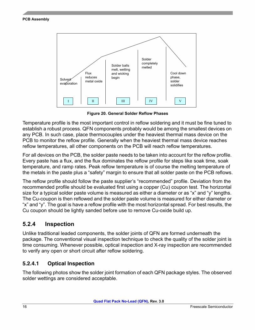
5.2.3 Reflow SolderingThe purpose of the reflow process is to melt the solder particles, wet the surfaces to be joined and at last, solidify the solder into a stronger metallurgical bond. Prior to the melting phase, several other phases occur and the sequence of events is described in Figure 20.
Feed Direction
Quad Flat Pack No-Lead (QFN), Rev. 3.016 Freescale Semiconductor
PCB Assembly
Figure 20. General Solder Reflow Phases
Temperature profile is the most important control in reflow soldering and it must be fine tuned to establish a robust process. QFN components probably would be among the smallest devices on any PCB. In such case, place thermocouples under the heaviest thermal mass device on the PCB to monitor the reflow profile. Generally when the heaviest thermal mass device reaches reflow temperatures, all other components on the PCB will reach reflow temperatures.
For all devices on the PCB, the solder paste needs to be taken into account for the reflow profile. Every paste has a flux, and the flux dominates the reflow profile for steps like soak time, soak temperature, and ramp rates. Peak reflow temperature is of course the melting temperature of the metals in the paste plus a �safety� margin to ensure that all solder paste on the PCB reflows.
The reflow profile should follow the paste supplier�s �recommended� profile. Deviation from the recommended profile should be evaluated first using a copper (Cu) coupon test. The horizontal size for a typical solder paste volume is measured as either a diameter or as �x� and �y� lengths. The Cu-coupon is then reflowed and the solder paste volume is measured for either diameter or �x� and �y�. The goal is have a reflow profile with the most horizontal spread. For best results, the Cu coupon should be lightly sanded before use to remove Cu-oxide build up.
5.2.4 InspectionUnlike traditional leaded components, the solder joints of QFN are formed underneath the package. The conventional visual inspection technique to check the quality of the solder joint is time consuming. Whenever possible, optical inspection and X-ray inspection are recommended to verify any open or short circuit after reflow soldering.
5.2.4.1 Optical Inspection
The following photos show the solder joint formation of each QFN package styles. The observed solder wettings are considered acceptable.
Solder balls
melt, wetting
and wicking
beginSolvent
evaporation
Flux
reduces
metal oxide
Solder
completely
melted
Cool down
phase,
solder
solidifies
I II III IV V

Quad Flat Pack No-Lead (QFN), Rev. 3.0Freescale Semiconductor 17
PCB Assembly
Figure 21. Optical Photos of QFN Solder Joints
5.2.4.2 X-Ray Inspection
X-ray is one way to detect solder shorts underneath the QFN package. X-rays transmitted from the X-ray tube are absorbed by the components in proportion to their density. In this case, a solder joint having a higher density absorbs most of the X-rays and the resultant X-ray intensity is detected and interpreted in gray scale image as shown in the photo in Figure 22. The X-ray image is also a good instrument to view solder voids in the exposed pad region.
Figure 22. X-Ray of 9 x 9 mm QFN Package
MAP QFN �E� Version
MAP QFN �S� Version
Punch Singulated Version

Quad Flat Pack No-Lead (QFN), Rev. 3.018 Freescale Semiconductor
PCB Assembly
5.2.4.3 Micro-Sectioning
Micro-sectioning is another method of inspecting solder joints. This method is not ideal for production inspection, but a tool to inspect the condition of the solder fillet. Figure 23 shows pictures of solder joints from different styles of QFN packages.
Figure 23. Micro-Sectioning of Various Style of QFN
5.2.4.4 Conventional Visual Inspection
The MAP style QFN is difficult to inspect from the top of the package compared to the punch singulated style. It may be necessary to tilt the PCB to inspect solder joints for the MAP style QFNs.
Molding
Compound
Leadframe
Solder
PCB Copper
Pad
ThermalExposed Pad
Solder
Thermal
PadMAP QFN “E” Style
MAP QFN “S” Style Punch Singulated QFN Style

Quad Flat Pack No-Lead (QFN), Rev. 3.0Freescale Semiconductor 19
PCB Assembly
5.3 Rework ProcedureQFN components removed during PCB rework should not be reused for final assemblies. Freescale [2] follows standard component level qualifications for packages/components and these include three solder reflows� survivability. A package that has been attached to a PCB and then removed has seen two solder reflows and if the PCB is double sided, the package has seen three solder reflows. Thus the package is at or near the end of the tested and qualified range of known survivability. These removed QFN components should be properly disposed of so that will not mix in with fresh equivalent QFN components.
5.3.1 Package RemovalIn general, the rework station should have a split light system, an XY table for alignment and a hot air reflow system with top and bottom heater for component removal.
To remove the faulty component from the board, hot air should be applied from the top and bottom heaters. An air nozzle with correct size should be used to conduct the heat to the QFN component such that the vacuum pick up tool can properly remove the component. The temperature for the top heater was set at 300°C for 30 seconds and the bottom heater applied simultaneously at 150°C for 30 seconds. The pictoral procedure is shown in Figure 24. Many assembly sites have extensive in-house knowledge on rework and their experts should be consulted for further guidance.
Figure 24. Package Removal Process
5.3.2 Site PreparationOnce the QFN component is removed, the site is cleaned and dressed to prepare for the new component placement. A de-soldering station can be used for solder dressing. It should be noted that the applied temperature should not be >245°C. Otherwise the copper pad on the PCB may peel off.
Load PCB on XY Table Select Appropriate Nozzle Removal

Quad Flat Pack No-Lead (QFN), Rev. 3.020 Freescale Semiconductor
PCB Assembly
5.3.3 Solder Paste PrintingA mini-stencil (see Figure 25) with the same stencil thickness, aperture opening and pattern as the normal stencil are placed in the component site. A mini-metal squeegee blade deposits solder paste in the specific area. The printed pad should be inspected to ensure even and sufficient solder paste before component placement.
Figure 25. Mini-Stencil for Solder Paste Printing
In situations where neighboring parts are at close proximity with the QFN components and the mini-stencil method is not an option, apply solder paste carefully on each pad using a syringe. The volume of solder paste will be difficult to control.
5.3.4 Component PlacementA vacuum nozzle is used to pick the new package up. The split light system displays images of both the QFN leads and the footprint on the PCB. The two superimposed images are aligned manually by adjusting the XY table. Once the PCB and the package are aligned, the package is placed down on the PCB (see Figure 26).
Figure 26. Component Placement Process
5.3.5 Reflow SolderingThe replaced component is then soldered to the PCB using the same temperature profile similar to the normal reflow soldering process.
PCB Image Capture by Camera Superimpose QFN on PCB

Quad Flat Pack No-Lead (QFN), Rev. 3.0Freescale Semiconductor 21
Moisture Sensitivity Level Rating
6.0 Moisture Sensitivity Level RatingThe Moisture Sensitivity Level (MSL) indicates the floor life of the component and its storage conditions after the original container has been opened. The lower the MSL value, the less care is needed to store the components. The QFN MSL reliability is dependent upon the different supplier material set and package size. Table 6 depicts the best case MSL for each package size at the time of document release.
7.0 Board Level ReliabilityThe board level reliability is usually presented in terms of solder joint life. The solder joint results in this section utilized the board layout guidelines form Section 4.1.2.
7.1 Testing DetailsThe QFN package has a relatively short solder joint life compared to leaded packages. The solder joint reliability has been tested for reliability by Freescale to understand solder joint life and failure mechanism. The result is in terms of Time to First Failure (TFF) and Mean Time to Failure (MTTF) values.
Samples of QFN wirebonded in daisy chain format were used to study the solder joint reliability. Odd leads were wirebonded to the even leads (i.e.: 1-2, 3-4, 5-6, etc.) in sequence. A complementary pattern was designed on the test PCB to provide one electrical circuit (net) through the package when the package is attached to the test PCB.
Table 6. MSL on QFN Package
Pkg Size(mm)
Pitch(mm)
Lead Count MSL
4 x 4 (EP) 0.65 16 1 @ 240°C
4 x 4 (EP) 0.50 20 1 @ 240°C
4 x 4 (EP) 0.50 24 1 @ 240°C
5 x 5 (EP) 0.65 20 1 @ 240°C
5 x 5 (EP) 0.50 32 1 @ 240°C
7 x 7 (EP) 0.65 32 1 @ 240°C2 @ 260°C
7 x 7 (EP) 0.50 44 1 @ 240°C2 @ 260°C
7 x 7 (EP) 0.50 48 1 @ 240°C2 @ 260°C
8 x 8 0.50 56 2 @ 260°C
9 x 9 (EP) 0.65 44 2 @ 240°C

Quad Flat Pack No-Lead (QFN), Rev. 3.022 Freescale Semiconductor
Board Level Reliability
Figure 27. (L) Test PCB, (R) Daisy Chain QFN Package (Not to Scale)
The image on the left is an actual photograph from a 44ld 9 x 9 mm QFN PCB pad configuration. The package (X-ray photo shown) fits inside the white outlined area. The double wirebonds in the package were enhanced to show the daisy chain pattern. Test points exterior to the white outline allow one to isolate which pair of solder joints failed during testing.
Assembled PCBs can be temperature cycled at a variety of temperature ranges. The most common test conditions for Freescale are 0°C to 100°C and �40°C to 125°C temperature ranges. The 0°C to 100°C condition has 10 minute ramps between temperature extremes with 5 minute dwells at the temperature extremes. Dwell time and ramp time are 15 minutes each for the -40°C to 125°C condition.
The test process is air-to-air temperature cycling, where daisy chained components are monitored in a chamber with its air exchanged to cause the packages to reach the desired temperatures. This contrasts with air-to-air temperature shock, where the components are shuttled back and forth between two chambers at the temperature extremes. Freescale has the capability of continuously monitoring the resistance through a daisy chain package and its complementary test PCB. Failure is defined as resistance through the daisy chain net of 300 Ohms or greater. Daisy chain nets are tested (time zero testing) prior to temperature cycling. Most nets start with initial resistance below 10 Ohms.
7.2 Solder Joint Reliability (SJR) ResultsFreescale [6] continues to work on understanding and improving the solder joint reliability of QFN packages. From the various experiments, the best �time to first failure� values are provided in Table 7 and Table 8 for the different package size, lead count and pitch. These results were obtained after several iterations. Contact local Product Package Engineer to obtain specifics on PCB and stencil design layouts. All experiments were performed using similar size test boards.

Quad Flat Pack No-Lead (QFN), Rev. 3.0Freescale Semiconductor 23
Board Level Reliability
Table 7. Best Case TTF on QFN, Sorted by Package Size and Lead Count
Pkg Size(mm)
Pitch(mm)
Lead Count Temp Cycle Time to First Failure
(cycles)
5 x 5 (EP) 0.65 20 0 to 100°C 2958
5 x 5 (EP) 0.65 20 -40 to 125°C 1740
5 x 5 (EP) 0.50 32 0 to 100°C 3048
5 x 5 (EP) 0.50 32 -40 to 125°C 1853
7 x 7 (EP) 0.65 32 0 to 100°C 5057
7 x 7 (EP) 0.65 32 -40 to 125°C >2000
7 x 7 (EP) 0.50 44 0 to 100°C 4914
7 x 7 (EP) 0.50 44 -40 to 125°C 1505
7 x 7 (EP) 0.50 48 0 to 100°C 3950
7 x 7 (EP) 0.50 48 -40 to 125°C 1340
8 x 8 0.50 56 0 to 100°C 1293
8 x 8 0.50 56 -40 to 125°C 621
9 x 9 (EP) 0.65 44 -40 to 125°C >3500
Table 8. Best Case TTF on QFN, Sorted by Pitch, Temp Cycle and Package Size
Pkg Size(mm)
Pitch(mm)
Lead Count Temp Cycle Time to First Failure
(cycles)
5 x 5 (EP) 0.50 32 0 to 100°C 3048
7 x 7 (EP) 0.50 44 0 to 100°C 4914
7 x 7 (EP) 0.50 48 0 to 100°C 3950
8 x 8 0.50 56 0 to 100°C 1293
5 x 5 (EP) 0.50 32 -40 to 125°C 1853
7 x 7 (EP) 0.50 44 -40 to 125°C 1505
7 x 7 (EP) 0.50 48 -40 to 125°C 1340
8 x 8 0.50 56 -40 to 125°C 621
5 x 5 (EP) 0.65 20 0 to 100°C 2958
7 x 7 (EP) 0.65 32 0 to 100°C 5057
5 x 5 (EP) 0.65 20 -40 to 125°C 1740
7 x 7 (EP) 0.65 32 -40 to 125°C >2000
9 x 9 (EP) 0.65 44 -40 to 125°C >3500

Quad Flat Pack No-Lead (QFN), Rev. 3.024 Freescale Semiconductor
Package Thermal Resistances
7.3 Increasing SJR for High Reliability ApplicationsThe QFN package is one of the promising candidates in replacing bigger leaded packages. This package is able to accommodate a larger die size for the same package size. On the flip side, leaded packages have among the longest SJR life of all packages due to its lead shape and its ability to reduce the stress from coefficient of thermal expansion mismatch.
A majority of the study for SJR in high reliability applications have been conducted with 7 x 7 mm and 9 x 9 mm 0.65 mm pitch packages. Several iterations of board and stencil designs were required to meet SJR of greater than 2000 TTF for these two package sizes. For high reliability applications, Freescale recommends evaluating the QFN package on a case by case basis. This applies to all lead count and package sizes. The TTF values provided in Table 7 and Table 8 are highly dependent upon many factors. If repeatability is taken into account, the typical TTF values would be lower than the values shown in Table 7 and Table 8.
8.0 Package Thermal ResistancesThe thermal performance of the QFN package is characterized using two thermal board types and three boundary conditions. Junction-to-ambient thermal resistance (Theta-JA or RθJA per JEDEC EIA/JESD51-2 [7]) is a one-dimensional value that measures the conduction of heat from the junction (hottest temperature on die) to the environment near the package. The heat that is generated on the die surface reaches the immediate environment along two paths: (1) convection and radiation off the exposed surface of the package and (2) conduction into and through the test board followed by convection and radiation off the exposed board surfaces. RθJA measures the thermal performance of the package in a low conductivity test board (single signal layer � 1s) in a natural convection environment. The 1s test board is designed per JEDEC EIA/JESD51-3 [8] and JEDEC EIA/JESD51-5 [9]. Another thermal resistance that is commonly reported is Theta-JMA or RθJMA on a board with two signal layers and two internal planes (2s2p). The 2s2p test board is designed per JEDEC EIA/JESD51-5 [9] and JEDEC EIA/JESD51-7 [10]. RθJA and RθJMA help bound the thermal performance of the QFN package in a customer�s application. RθJA helps estimate the thermal performance of the QFN package when it is mounted in two distinct configurations: (1) a board with no internal thermal planes (i.e., low conductivity board) or (2) when a multi-layer board is tightly populated with similar components. RθJMA provides the thermal performance of the QFN when there are no nearby components dissipating significant amounts of heat on a multi-layer board. Junction-to-board thermal resistance (Theta-JB or RθJB per JEDEC EIA/JESD51-8 [11]) is also provided for the QFN package. RθJB measures the horizontal spreading of heat between the junction and the board. The board temperature is taken 1 mm from the package on a board trace located on the top surface of the board. Another thermal resistance that is provided is junction-to-case thermal resistance (Theta-JC or RθJC). The case is defined at the exposed pad surface. RθJC can be used to estimate the thermal performance of the QFN package when the board is adhered to a metal housing or heat sink and a complete thermal analysis is done. These thermal resistances help bound the thermal problem under distinct environments.
Table 9 has some thermal information for certain QFN packages. All of the data was generated using Silicon (Si) die. There is an inverse relationship between the body size of the package and

Quad Flat Pack No-Lead (QFN), Rev. 3.0Freescale Semiconductor 25
Package Thermal Resistances
the thermal resistances. Large packages have lower RθJMA values. The greater the body size, the larger the exposed pad, and the more PTH vias will fit under the exposed pad. The low RθJC values indicate that this package is capable of dissipating 5 Watts when the bottom surface of the board is heat sunk and there is a 45°C junction-to-heat sink temperature difference [13].
Table 9. Thermal Resistances for Various QFN Packages
I/O Body Sizemm x mm
Pitchmm
Flag Sizemm x mm
Die Sizemm x mm
RθJA(1),(2)
°C/WRθJMA
(1),(3)
°C/WRθJB
(4)
°C/WRθJC
(5)
°C/W
12 3 x 3 0.50 1.2 x 1.2 0.3 x 0.3 277 152 122 97
12 3 x 3 0.50 1.2 x 1.2 0.56 x 0.56 230 102 72 41
12 3 x 3 0.50 1.2 x 1.2 0.8 x 0.8 213 85 56 21
16 4 x 4 0.65 2.0 x 2.0 0.56 x 0.56 196 79 57 39
16 4 x 4 0.65 2.0 x 2.0 0.95 x 0.95 173 56 34 16
16 4 x 4 0.65 2.0 x 2.0 1.1 x 1.1 168 52 30 12
16 4 x 4 0.65 2.0 x 2.0 1.6 x 1.6 157 46 23 6
20 4 x 4 0.50 2.1 x 2.1 0.56 x 0.56 179 78 56 40
20 4 x 4 0.50 2.1 x 2.1 1.05 x 1.05 154 53 30 13
20 4 x 4 0.50 2.1 x 2.1 1.2 x 1.2 150 50 27 11
20 4 x 4 0.50 2.1 x 2.1 1.7 x 1.7 140 44 22 6
24 4 x 4 0.50 2.25 x 2.25 0.56 x 0.56 178 79 58 40
24 4 x 4 0.50 2.25 x 2.25 1.2 x 1.2 150 50 29 11
24 4 x 4 0.50 2.25 x 2.25 1.35 x 1.35 147 48 27 9
24 4 x 4 0.50 2.25 x 2.25 1.85 X 1.85 139 43 22 5
32 5 x 5 0.50 3.1 x 3.1 0.56 x 0.56 154 71 52 39
32 5 x 5 0.50 3.1 x 3.1 2.2 x 2.2 116 34 15 3.4
32 5 x 5 0.50 3.1 x 3.1 2.7 x 2.7 111 32 13 2.3
32 5 x 5 0.50 3.1 x 3.1 2.9 x 2.9 108 32 13 2.0
32 7 x 7 0.65 4.7 x 4.7 2.16 x 2.16 96 30 13 3.5
32 7 x 7 0.65 4.7 x 4.7 3.8 x 3.8 90 27 10 1.2
32 7 x 7 0.65 5.1 x 5.1 4.3 x 4.3 97 26 9 0.9
44 7 x 7 0.50 5.1 x 5.1 2.56 x 2.56 81 26 10 2.5
44 7 x 7 0.50 5.1 x 5.1 4.2 x 4.2 76 24 7 1.0
44 7 x 7 0.50 5.1 x 5.1 4.7 x 4.7 74 23 7 0.8
48 7 x 7 0.50 5.1 x 5.1 2.56 x 2.56 84 26 10 2.5
48 7 x 7 0.50 5.1 x 5.1 4.2 x 4.2 79 24 8 1.0
48 7 x 7 0.50 5.1 x 5.1 4.7 x 4.7 77 23 7 0.8

Quad Flat Pack No-Lead (QFN), Rev. 3.026 Freescale Semiconductor
Electrical Performance
Notes: 1. Junction temperature is a function of die size, on-chip power dissipation, package thermal resistance, mounting site (board)
temperature, ambient temperature, power dissipation of other components on the board, and board thermal resistance.2. JEDEC EIA/JESD51-2 with the single layer board horizontal. Board conforms to JEDEC EIA/JESD51-3 and JEDEC
EIA/JESD51-5.3. Per JEDEC JESD51-6 with the board horizontal. Board conforms to JEDEC EIA/JESD51-5 and JEDEC EIA/JESD51-7.4. Thermal resistance between the die and the printed circuit board per JEDEC EIA/JESD51-8. Board temperature is measured
on the top surface of the board near the package.5. Thermal resistance between the die and the exposed pad without thermal grease.
9.0 Electrical PerformanceAs a leadless package, the series inductance and capacitance contributed by the QFN terminals are lower than those of leaded packages such as the TQFP and TSSOP, and those of BGA packages (due to the parasitic effects contributed by the substrate traces). This reduction in parasitic effects gives the QFN package a significant advantage over these other packages for RF applications. It is important to note, however, that the RLC (RLC stands for resistance, inductance and capacitance) performance comprises contributions of both the terminal and bonding wire. In cases of small die to flag size ratio, longer bonding wires may be required for the QFN than for the same device in a leaded package or BGA. In these cases, the RLC performance may be poorer for the QFN package. Therefore, it should not be assumed that the QFN will provide better electrical performance for all devices as the die size and bonding wire length must be considered.
Another advantage of the QFN package with regard to electrical performance is that the wires may be bonded to the exposed center pad, allowing better grounding compared to traditional leaded and BGA packages.
Electrical modeling has been performed to simulate the RLC performance of the 7 x 7 mm, 48-lead 0.5 mm pitch QFN package [14]. Figure 28 shows the package and wire SPICE model used for the simulation. SPICE stands for �Simulation Program with Integrated Circuit Emphasis.� It is a simulation tool used to design circuits.
I/O Body Sizemm x mm
Pitchmm
Flag Sizemm x mm
Die Sizemm x mm
RθJA(1),(2)
°C/WRθJMA
(1),(3)
°C/WRθJB
(4)
°C/WRθJC
(5)
°C/W
44 9 x 9 0.65 6.7 x 6.7 4.16 x 4.16 70 23 7 1.0
44 9 x 9 0.65 6.7 x 6.7 5.8 x 5.8 67 21 6 0.5
44 9 x 9 0.65 6.7 x 6.7 6.3 x 6.3 65 21 6 0.4
64 9 x 9 0.50 7.1 x 7.1 4.56 x 4.56 64 22 7 0.8
64 9 x 9 0.50 7.1 x 7.1 6.2 x 6.2 61 21 6 0.5
64 9 x 9 0.50 7.1 x 7.1 6.7 x 6.7 59 21 6 0.4
Table 9. Thermal Resistances for Various QFN Packages (continued)

Quad Flat Pack No-Lead (QFN), Rev. 3.0Freescale Semiconductor 27
Electrical Performance
Figure 28. SPICE Model
The simulations yielded self inductance values for the QFN package leads of 1.04 to 1.05 x 10⁻¹¹ H compared to similarly obtained values for TQFP leads of 1.11 to 1.39 x 10⁻⁹ H (4), fully two orders of magnitude lower for the QFN.
Figure 29 compares self-inductance values of the two packages including the contributions from both bonding wire and lead. The bonding wire is assumed to be approximately the same length in the two packages. In the case of the QFN, the contribution to inductance of the leads is negligible, and the only significant contribution to inductance is that of the bonding wire. The average value for the TQFP package is 3.27 nH, while that for the QFN is 2.06 nH, a 37% decrease.
Figure 29. Electrical Modeling of 7 x 7 mm 48ld QFN vs. 48ld TQFP
Additional self-inductance results from 32ld 0.65 mm pitch 7 x 7 mm and 44ld 065 mm pitch 9 x 9 mm packages are provided in Figure 30. Self-inductance of different die sizes was plotted for each package size. Note that the results between 32ld 7 x 7 mm and 44ld 9 x 9 mm QFN packages were very similar.
N01I
R01 WB
N01W
L01WB
N01R
R01
C01
L01
N01C N01O
System Board
BD_GND
WIRE LEAD
Self Inductance: Leads + Bonding Wire
0.000.501.001.502.002.503.003.504.00
1 4 7 10 13 16 19 22 25 28 31 34 37 40 43 46
Lead Number
Inductance,nH
TQFPQFN

Quad Flat Pack No-Lead (QFN), Rev. 3.028 Freescale Semiconductor
Electrical Performance
Figure 30. 32ld 7 x 7 mm and 48ld QFN 9 x 9 mm QFN Self-Inductance Chart
Figure 31 compares the simulated values of self-capacitance for 7 x 7 mm 48-lead TQFP and QFN packages (lead pitch of both packages in 0.50 mm). Averages values are 3.02 x 10⁻² and 1.20 x 10⁻¹ pF for the QFN and TQFP packages, respectively.
Figure 31. 48ld TQFP vs. QFN Package
The RLC circuit model (see Figure 32) may be used to predict frequency bandwidth for a package based on the transfer function between the circuit input and output nodes. By using such a methodology, the 3 dB cut-off frequency of a package can be predicted. The graph in Figure 32 shows the simulated frequency response for the longest wire of a new device packaged in the 48-lead 7 x 7 mm QFN package. The predicted value for cut-off frequency is 2.85 GHz. For a device packaged in a 48ld 7 x 7 mm TQFP package, a value of approximately 1.5 GHz would be typical.
Self Inductance: Leads + Bonding Wire
0.00
0.50
1.00
1.50
2.00
2.50
3.00
0 10 20 30
Lead Number
Inductance,nH
Die Size = 3.43 mm x 3.43 mm
Die Size = 2.16 mm x 2.16 mm
Die Size = 4.50 mm x 4.50 mm
Self Inductance: Leads + Bonding Wire
0.00
0.50
1.00
1.50
2.00
2.50
3.00
0 10 20 30 40
Lead Number
Inductance,nH
Die Size = 5.43 mm x 5.43 mm
Die Size = 6.30 mm x 6.30 mm
Die Size = 4.16 mm x 4.16 mm
32ld 0.65mm Pitch 7x7 mm QFN 44ld 0.65mm Pitch 9x9 mm QFN
Self Capacitance
0.000E+00
5.000E-14
1.000E-13
1.500E-13
2.000E-13
2.500E-13
1 4 7 10 13 16 19 22 25 28 31 34 37 40 43 46Lead Number
Cap
acita
nce
QFNTQFP

Quad Flat Pack No-Lead (QFN), Rev. 3.0Freescale Semiconductor 29
Electrical Performance
Figure 32. Bandwidth Characteristics of 48ld QFN
In order to experimentally compare the performance of the QFN to a QFP package in a manufacturing final test environment, an experiment was run in which known good die from the same wafer of an RF device were packaged in 48-ld QFN and 48-ld LQFP packages, 1000 of each test vehicle. The packaged devices were then processed through final parametric electrical testing. Results are shown in Table 10. The superior RF performance of the QFN package can be seen particularly in the Receive Signal Strength Indicator test (RF_STAGE_GAIN, Test 3) and Signal plus Noise and Distortion test (SINAD, Test 8). The values for the QFN package were higher in these tests by 1.9 dB and 5.1 dB respectively.
Table 10.
Test # Test Name UnitsQFN Data LQFP Data Delta in
MeanMean Std. Dev. Mean Std. Dev.
1 ICC_3.6V mA 24.8 0.39 27.6 0.45 -2.8
2 ICC_EN_LO µA 1.90 0.80 2.39 0.74 -0.49
3 RF_STAGE_GAIN dB 21.6 0.71 19.7 0.75 1.9
4 RSSI_1@-10dBm µA -39.1 1.26 -37.1 1.39 -2
5 RSSI_1@-50dBm µA -21.6 0.82 -20.3 0.91 -1.3
6 RSSI_1@-90dBm µA -3.57 0.37 -4.38 0.53 0.81
7 RSSI_SLOPE(µA/dB) µA/dB -0.44 0.01 -0.41 0.02 -0.03
8 SINAD@110dBm dB 24.04 1.04 18.93 1.51 5.11

Quad Flat Pack No-Lead (QFN), Rev. 3.030 Freescale Semiconductor
Reference
10.0 Reference[1] JEDEC Solid State Product Outline for Thermally Enhanced Plastic Very Thin and Very Very Thin Fine Pitch Quad Flat No Lead Package, MO-220, Rev. A, January, 2000.
[2] S. Lam, �Application Study Report, Quad Flat No-Lead (QFN) Surface Mount Assembly�, December, 2001.
[3] Courtesy of QFN supplier.
[4] EIA-783, �Guideline Orientation Standard for Multi-Connection Package (Design Rules for Tape and Reel Orientation)�, November 1998.
[5] W.W. Chow, Freescale SPS Internal QFN Presentation, 2000.
[6] T. Koschmieder, Freescale SPS Internal QFN Reliability Report, 2001.
[7] EIA/JESD51-2, �Integrated Circuits Thermal Test Method Environment Conditions � Natural Convection (Still Air)�, December 1995.
[8] EIA/JESD51-3, �Low Effective Thermal Conductivity Test Board for Leaded Surface Mount Packages,� August 1996.
[9] EIA/JESD51-5, �Extension of Thermal Test Board Standards for Packages with Direct Thermal Attachment Mechanisms,� February 1999.
[10] EIA/JESD51-7, �High Effective Thermal Conductivity Test Board for Leaded Surface Mount Packages,� February 1999.
[11] EIA/JESD51-8, �Integrated Circuit Thermal Test Method Environmental Conditions � Junction-to-Board�, October 1999.
[12] EIA/JESD 51-6, �Integrated Circuits Thermal Test Method Environment Conditions � Forced Convection (Moving Air),� March 1999.
[13] T. Montes de Oca, T. Koschmieder, B. Joiner, "Impact of Board Variables on the Thermal Performance of a QFN Package�, 2001.
9 DEMOD(PK-PK) V 0.92 0.04 0.94 0.03 -0.02
10 PRESCLR_64(PK-PK) V 0.49 0.01 0.48 0.01 0.01
11 PRESCLR_64(MHZ) MH 16.73 1.23 16.73 0.45 0
12 PRESCLR_65(PK-PK) V 0.50 0.01 0.49 0.01 0.01
13 PRESCLR_65(MHZ) MH 16.47 1.21 16.47 0.49 0
Table 10. (continued)
Test # Test Name UnitsQFN Data LQFP Data Delta in
MeanMean Std. Dev. Mean Std. Dev.

How to Reach Us:
Home Page:www.freescale.com
E-mail:[email protected]
USA/Europe or Locations Not Listed:Freescale SemiconductorTechnical Information Center, CH3701300 N. Alma School Road Chandler, Arizona 85224 +1-800-521-6274 or [email protected]
Europe, Middle East, and Africa:Freescale Halbleiter Deutschland GmbHTechnical Information CenterSchatzbogen 781829 Muenchen, Germany+44 1296 380 456 (English)+46 8 52200080 (English)+49 89 92103 559 (German)+33 1 69 35 48 48 (French)[email protected]
Japan:Freescale Semiconductor Japan Ltd. Headquarters ARCO Tower 15F 1-8-1, Shimo-Meguro, Meguro-ku, Tokyo 153-0064 Japan 0120 191014 or +81 3 5437 [email protected]
Asia/Pacific:Freescale Semiconductor Hong Kong Ltd.Technical Information Center 2 Dai King Street Tai Po Industrial Estate Tai Po, N.T., Hong Kong +800 2666 [email protected]
For Literature Requests Only:Freescale Semiconductor Literature Distribution CenterP.O. Box 5405Denver, Colorado 802171-800-441-2447 or 303-675-2140Fax: [email protected]
AN1902Rev. 3.012/2005
RoHS-compliant and/or Pb-free versions of Freescale products have the functionality and electrical characteristics of their non-RoHS-compliant and/or non-Pb-free counterparts. For further information, see http://www.freescale.com or contact your Freescale sales representative.
For information on Freescale�s Environmental Products program, go to http://www.freescale.com/epp.
Information in this document is provided solely to enable system and software implementers to use Freescale Semiconductor products. There are no express or implied copyright licenses granted hereunder to design or fabricate any integrated circuits or integrated circuits based on the information in this document.
Freescale Semiconductor reserves the right to make changes without further notice to any products herein. Freescale Semiconductor makes no warranty, representation or guarantee regarding the suitability of its products for any particular purpose, nor does Freescale Semiconductor assume any liability arising out of the application or use of any product or circuit, and specifically disclaims any and all liability, including without limitation consequential or incidental damages. �Typical� parameters that may be provided in Freescale Semiconductor data sheets and/or specifications can and do vary in different applications and actual performance may vary over time. All operating parameters, including �Typicals�, must be validated for each customer application by customer�s technical experts. Freescale Semiconductor does not convey any license under its patent rights nor the rights of others. Freescale Semiconductor products are not designed, intended, or authorized for use as components in systems intended for surgical implant into the body, or other applications intended to support or sustain life, or for any other application in which the failure of the Freescale Semiconductor product could create a situation where personal injury or death may occur. Should Buyer purchase or use Freescale Semiconductor products for any such unintended or unauthorized application, Buyer shall indemnify and hold Freescale Semiconductor and its officers, employees, subsidiaries, affiliates, and distributors harmless against all claims, costs, damages, and expenses, and reasonable attorney fees arising out of, directly or indirectly, any claim of personal injury or death associated with such unintended or unauthorized use, even if such claim alleges that Freescale Semiconductor was negligent regarding the design or manufacture of the part.
Freescale� and the Freescale logo are trademarks of Freescale Semiconductor, Inc. All other product or service names are the property of their respective owners.© Freescale Semiconductor, Inc., 2005. All rights reserved.