Embed Size (px)
Citation preview
1/30
AN1792APPLICATION NOTE
November 2003
IntroductionTwo methods of controlling Power Factor Corrector (PFC) pre-regulators based on boost topology are cur-rently in use: the Fixed-Frequency (FF) PWM and the Transition Mode (TM) PWM (fixed ON-time, variablefrequency). The first method employs average current-mode control, a relatively complex technique requiringsophisticated controller IC's (e.g. STMicroelectronics' L4981A/B) and a considerable component count. Thesecond one uses the simpler peak current-mode control, which is implemented with cheaper controller IC's(e.g. STMicroelectronics' L6561, L6562), much fewer external parts and is therefore much less expensive.
With the first method the boost inductor works in Continuous Conduction Mode (CCM), while TM makesthe inductor work on the boundary between continuous and discontinuous mode, by definition. For a givenpower throughput, TM operation then involves higher peak currents as compared to FF-CCM (see figure1). This, also consistently with the above mentioned cost considerations, suggests the use of TM in a lowerpower range, while FF-CCM is recommended for higher power levels.
This criterion, though always true, is sometimes difficult to apply, especially for a midrange power level, sayaround 150-300W. The assessment of which approach gives the better cost/performance trade-off needs tobe done on a case-by-case basis, considering the cost and the stress of not only power semiconductors andmagnetics but also of the EMI filter: at the same power level, the switching frequency component to be fil-tered out in a TM system is twice the line current, whereas it is typically 1/3 or 1/4 in a CCM system.
Figure 1. Line, inductor, switch and diode currents in: a) FF-CCM PFC, b)TM PFC.
Inductor current peak envelope
ON
OFFSwitch
ILpk
Diode currentSwitch current
Low frequencyinductor current
ON
OFFSwitch
Switch current Diode current
Low frequencyinductor current Inductor current
a) FF-CCM control b) TM control
by C. Adragna
DESIGN OF FIXED-OFF-TIME-CONTROLLEDPFC PRE-REGULATORS WITH THE L6562
Beside Transition Mode (TM) and fixed-Frequency Continuous Conduction Mode (FF-CCM) operationof PFC pre-regulators a third approach is proposed that couples the simplicity and affordability of TMoperation with the high current capability of FF-CCM operation: it is a peak current-mode control withfixed-OFF-time. After showing advantages and limits of this technique, in both its basic and advancedimplementation, design equations will be given and a practical design will be illustrated and evaluated.

AN1792 APPLICATION NOTE
2/30
In this area where the TM/CCM usability boundary is uncertain, a third approach that couples the simplicityand affordability of TM operation with the high current capability of CCM operation can be a solution to thedilemma.
Generally speaking, FF PWM is not the only alternative when CCM operation is desired. FF PWM modu-lates both switch ON and OFF times (their sum is constant by definition), and a given converter will operatein either CCM or DCM depending on the input voltage and the loading conditions. Exactly the same resultcan be achieved if the ON-time only is modulated and the OFF-time is kept constant, in which case, how-ever, the switching frequency will not be fixed anymore (see figure 2). This is referred to as "Fixed-OFF-Time" (FOT) control. Peak-current-mode control can still be used.
Figure 2. Basic waveforms for Fixed-frequency PWM (a) and Fixed-OFF-Time PWM (b)
The concept of FOT control is not new [1], [2] but, to the author's knowledge, it has never been applied toPFC pre-regulators to allow CCM operation. In addition to the many advantages and the few drawbacksthat this control technique brings to PFC pre-regulators and that will be highlighted in the following sec-tions, an important point is that FOT control does not need a specialized control IC. A simple modificationof a standard TM PFC controller operation, requiring just few additional passive parts and no significantextra cost, is all that is needed.
Operation of a FOT-controlled PFC pre-regulator and its practical implementationFigure 3 shows a block diagram of a FOT-controlled PFC pre-regulator. An error amplifier (VA) comparesa portion of the pre-regulator's output voltage Vout with a reference VREF and generates an error signalVC proportional to their difference. VC, a DC voltage by hypothesis, is fed into an input of the multiplierblock and there multiplied by a portion of the rectified input voltage VMULT. At the output of the multiplier,there will be a rectified sinusoid, VCSREF, whose amplitude is proportional to that of VMULT and to VC,which represents the sinusoidal reference for PWM modulation. VCSREF is fed into the inverting input of acomparator that, on the non-inverting input, receives the voltage VCS on the sense resistor Rsense, pro-portional to the current flowing through the switch M (typically a MOSFET) and the inductor L during theON-time of M. When the two voltages are equal, the comparator resets the PWM latch and M, supposedalready ON, will be switched off.
a) Fixed Frequency
Gate drivesignal
TON
TON'
TON
TON'
TON
TON'
TOFF
TOFF'
TOFF
TOFF'
TSW TSW
a) Fixed OFF-TIme
Gate drivesignal
TON TON TON TOFF
TOFF
TSW TSW
TSW' TSW' TON' TON' TON'
TOFF
TOFF

3/30
AN1792 APPLICATION NOTE
Figure 3. Block diagram of an FOT-controlled PFC pre-regulator.
As a result, VCSREF determines the peak current through M and the inductor L. As VCSREF is a rectifiedsinusoid, the inductor peak current will be enveloped by a rectified sinusoid as well. The line current Iinwill be the average inductor current, that is the low frequency component of the inductor current resultingfrom the low-pass filtering operated by the EMI filter.The PWM latch output Q going high activates the Timer that, after a predetermined time TOFF has elapsed,sets the PWM latch, thus turning M on and starting another switching cycle. If TOFF is such that the induc-tor current does not fall to zero, the system will operate in CCM.
It is apparent that FOT control requires nearly the same architecture as TM control, just the way the OFF-time of M is determined changes. It is not a difficult task to modify externally the operation of standard TMPFC controller so that the OFF-time of M is fixed. As a controller we will refer to the L6562 [4], which is suit-able for a few hundred watts power applications because of its gate drive capability and its high noise im-munity.The circuit that implements FOT control with the L6562 is shown in figure 4 along with some relevantwaveforms. During the ON-time of M the gate voltage VGD is high, the diode D is forward-biased and thevoltage at the ZCD pin is internally clamped at VZCDclamp ≈ 5.7V. During the OFF-time of M VGD is low,the diode D is reverse-biased and the voltage at the pin decays with an exponential law:
,
until it reaches the triggering threshold (VZCDtrigger ≈ 1.4V) that causes the switch to turn on. The time need-ed for the ZCD voltage to go from VZCDclamp to VZCDtrigger will define the duration of the OFF-time TOFF:
. (α)
Driver
Rsense
VA
VREF
VREF
L D
Cin CoM
R
QS
Multiplier
00
0
0
+
-
Frequencycompensation
TIMER(Fixed OFF-time generator)
Timer Start
0
Q
Vc
Vout
Vpk
R1
R2
VMULTVCSREF
Iin
PWMlatch
PWM+
-
Vcs
0
EMI FILTERVin =
88 to 264VAC
VZCD VZCDclampe
t–RC---------
=
TOFF RCVZCDclamp
VZCDtrigger------------------------------- 1.4 RC⋅≈ln=

AN1792 APPLICATION NOTE
4/30
As a practical rule, it is convenient to select a capacitor first and then to calculate the resistor needed toachieve the desired TOFF. As the gate voltage VGD goes high the resistor Rs charges the timing capacitorC as quickly as possible up to VZCDclamp, without exceeding clamp rating (IZCDx =10 mA). Then it mustfulfill the following inequalities:
, (β)
where VGD (assume VGD = 10V) is the voltage delivered by the gate driver, VGDx = 15V its maximumvalue, and VF the forward drop on D.
Figure 4. Circuit implementing FOT control with the L6562 and relevant timing waveforms.
When working at high line/light load the ON-time of the power switch becomes very short and the resistorRs alone is no more able to charge C up to VZCDclamp. The speed-up capacitor Cs is then used in parallelto Rs. This capacitor will cause an almost instantaneous charge of C up to a level, after that Rs will com-plete the charge up to VZCDclamp. It is important that the steep edge caused by Cs does not reach theclamp level, otherwise the internal clamp of the L6562 would undergo uncontrolled current spikes (limitedonly by the dynamic resistance of the 1N4148 and the ESR of Cs) that could overstress the IC. Cs mustthen be:
, (γ)
Implications of FOT control for CCM-operated PFC pre-regulators Essentially, the aim of FOT control in PFC pre-regulators is to allow CCM operation, and hence high powercapability, but with the same complexity level of a TM-operated PFC stage. This goal can be achievedsince the properties of FOT control enable the use of the simpler "peak current-mode" control rather thanthe more complex "average current-mode" needed by the FF-CCM approach.
In short, peak current-mode FOT control provides an unconditionally stable inner current loop with no gainpeaking and shows "dead-beat control" characteristics. Referring to reference [1] for a detailed explana-tion of these properties, it is useful to see how they affect the characteristics of FOT-CCM PFC pre-regu-lators.
1) Simple control, low part count. The absence of the sub-harmonic instability typical of FF-systems at dutycycles greater than 50% (see figure 5), makes FOT control very convenient in a PFC boost stage, wherethe duty cycle can theoretically reach 100%. FF-CCM using peak-current-mode results in an unstable sys-tem as long as the instantaneous line voltage is below half the regulated output voltage (condition for dutycycle >50%) with no slope compensation, unless the system is designed to run in DCM (Discontinuous
VGDx VZCDclamp VF––
IZCDx
VZCDclamp
R-----------------------------+
--------------------------------------------------------------- Rs RVGD VZCDclamp VF––
VZCDclamp-------------------------------------------------------------<<
without Cs
Pin 7
Pin 4
S
R
Q
TOFF TON
VREFCS
Pin 55.7V
1.4V
InternalPWM latch
signals(see fig. 3)
TOFF TOFF
Rs
5
L6562
7
D1N4148
R C Cs
ZCD
GDM
4CS
Rsense
Cs CVZCDclamp
VGDx VZCDclamp VF––---------------------------------------------------------------<

5/30
AN1792 APPLICATION NOTE
Conduction Mode) under these conditions. This is quite a limitation. This is why average-current-mode isusually preferred for FF-CCM operation, despite the penalty of an increased circuit complexity. Addition-ally, FOT control does not require the use of an auxiliary winding on the boost inductor as does the TMapproach. If the control IC can be powered by an external source (e.g. the transformer of a cascaded DC-DC converter) the inductor can be made with a single winding with some saving in its cost.
2) Dynamic behavior improvement. The optimum response of the inner current loop tends to limit inductorcurrent ringing resulting from load changes. However, it has little impact on the performance of the outervoltage control loop, still largely dominated by the low bandwidth needed to achieve a high PF.
Figure 5. FF vs. FOT control at D>50%: instability (FF) and stability with critical damping (FOT).
3) Reduced EMI emissions. Variable frequency operation is inherent in FOT concept: any variation of loadcurrent or input voltage is compensated by the feedback control with a variation of the switch ON-time.Thus, the switching frequency of a PFC pre-regulator is modulated, at a modulation rate twice the mainsfrequency, by the input voltage swinging all the way from zero to the peak. The result is a spread-spectrumaction that reduces the peak energy of the noise generated and simplifies the ability to comply with EMIregulations.
4) DCM and CCM always live together, at least at nominal load. Figure 6 shows typical current waveforms:at two points along the sinusoid the inductor current ripple during one switching cycle equals the peak val-ue in that cycle. This is the boundary between CCM and DCM operation: there will be DCM around theline voltage zero-crossings and CCM around the top of the sinusoid. As the power is reduced, the regionof DCM operation will get larger until it takes up the entire line cycle.
Figure 6. Typical current waveforms along a line voltage half-cycle of a FOT-controlled PFC stage.
5) Stress due to boost diode's reverse recovery and MOSFET's capacitive loss is alleviated. CCM opera-tion requires the use of ultra-fast recovery diodes. In the DCM portion, however, (typically, about 30% ofthe line cycle) the recovery of the boost diode is not invoked, hence the related losses in the diode itselfand those induced in the MOSFET are reduced. Additionally, because of the DCM portion, the capacitivelosses at MOSFET turn-on due to the discharge of the drain capacitance are decreased as well. Actually,during a small part of the DCM portion the MOSFET is soft-switched.
Inductorcurrent
time
programmed value
steady-state inductor current
perturbed inductor current
∆Ι0
∆Ι2
FIXED-FREQUENCY CONTROL
Dmax· Tsw
Tsw
1∆Ι
FIXED OFF-TIME CONTROL
Inductorcurrent
time
programmed value
same slope
T OFF T OFF
steady-state inductor currentperturbed inductor current
Inductor current peak envelopeInductor current rippleInductor average current
DCMDCM
0 0.52 1.05 1.57 2.09 2.62 3.14
q
CCM

AN1792 APPLICATION NOTE
6/30
6) Line current distortion is not negligible. It will be shown that as long as the system operates in CCM theline current waveform is a portion of a sinusoid but, as it enters DCM around the line voltage zero cross-ings, the shape changes, causing a distortion of the line current (see the dash-dot line in figure 6). How-ever, it will be shown that its harmonic contents is still comfortably compliant with EN61000-3-2 standardson harmonic current emissions. Thus the practical impact of this drawback is very limited.
7) Trade-off between operating frequency and line current distortion. It will be shown that, in order to limitline current distortion at high line, the OFF-time must be selected greater than a minimum value. Thiscould prevent the use of a switching frequency high enough to have a relatively small inductor size. How-ever, a variant of the basic FOT control will be presented that allows the designer to overcome this issue.
FOT-CCM PFC: large-signal characteristics. The large-signal characteristics of a FOT-CCM PFC boost pre-regulator will be now discussed from the qual-itative point of view. For details on the FOT-CCM PFC large signal model derivation, please refer to [3]. Thequantitative results of the approximate analysis described in [3], provided in tables 2, 3 and 4, are the basisfor a design procedure that will be outlined in another section.
It is well-known that in a boost converter, during the MOSFET's OFF-time TOFF (which is a given design pa-rameter), the inductor demagnetizes and releases the energy stored during the ON-time. If in a switching cy-cle TOFF is long enough to completely discharge the inductor within that cycle, there will be DCM operation,otherwise there will be CCM operation. As previously said, if the PFC boost is operated with FOT, DCM andCCM operation alternate in a line half-cycle. The phase angle θT ∈ [0, π/2] where the operation changesfrom DCM to CCM will be referred to as the "transition angle". Considering waveform symmetry, operationwill change from CCM back to DCM at the supplementary phase angle π - θT. In each line half-cycle therewill be CCM operation for θT < θ < π - θT and DCM operation for θ < θT and θ > π - θT. In a given converter(i.e. for given Vout, L and TOFF), the transition angle θT depends on the operating conditions (line voltageand output load). Figure 7 shows schematically the inductor current, also pointing out how it is split betweenthe MOSFET M and the diode D. The low-frequency component, that is the line current Iin(θ), is shown too.
Figure 7. Inductor, switch and diode currents in a CCM-FOT-controlled PFC stage.
During the DCM portion of the line half-cycle MOSFET's ON-time TON is constant and, as TOFF is constantby definition, the switching frequency and MOSFET duty cycle will be constant as well. Their value dependon the peak input voltage and the output load. During the CCM portion they change with both the peakand the instantaneous line voltage but not with the load. The switching frequency is maximum on the topof the sinusoid, reaches the minimum at the DCM/CCM boundary and does not change any more in theDCM portion.
ON OFFSwitch
Diode current
DCM
Switch current
TOFF
ILpk
π − θTθT
DCM
CCM Inductor current peak envelope
Low frequencyinductor current
TOFF

7/30
AN1792 APPLICATION NOTE
Table 1. List of basic symbols used in tables 2 to 4
Table 2. Timing quantities of FOT-controlled boost PFC pre-regulators
Table 3. Inductor and line input current in FOT-controlled boost PFC pre-regulators
As shown in figure 7, the inductor current will be a series of rising (during TON) and falling (during TOFF)ramps whose peaks are enveloped by ILpksinθ. In a single switching cycle, the current will always be tri-angular: in the DCM portion the triangles start from zero and touch zero before the end of the cycle, inCCM the triangles are superimposed on top of a current pedestal. The inductor current ripple is minimumon the top of the sinusoid and maximum at the transition DCM⇔CCM. Note that this property gives a prac-tical meaning to the transition phase angle θT; its sine provides the ratio of the maximum current rippleamplitude to the inductor peak current, the so-called "ripple factor" Kr, a parameter typically used in the
Symbol Parameter
TOFF Fixed MOSFET OFF-time
L Boost inductor’s inductance
Vpk Peak line voltage ( times the RMS value Vac)
Vout Pre-regulator’s output regulated voltage
Pout Pre-regulator’s output power
Pin Pre-regulator’s input power (= Pout / η , η = efficiency)
ILpk Peak of inductor current sinusoidal envelope
k Vpk/Vout ratio
Γ Conventional zero-voltage-input inductor current ripple: Vout·TOFF/L
Symbol Parameter DCM CCM
θT Transition angle (DCM⇒CCM boundary)
TON(θ) MOSFET ON-time
D(θ) MOSFET duty cycle 1 - ksinθT 1 - ksinθfsw(θ) Switching frequency
δfsw(θ) Switching frequency modulation depth
TFW(θ) Inductor demagnetization time TOFF
DL(θ) Inductor current circulation duty cycle 1
Symbol Parameter DCM CCM
∆IL(θ) Inductor current ripple ILpksinθ Γ(1 - k sinθ)
IL(av)(θ) Inductor average current
Iin(θ) Line input current
2
sin1– ΓILpk kΓ+-----------------------
LILpk
kVout--------------
1k θsin--------------- 1– TOFF
kTOFF-------------- θTsin k
TOFF-------------- θsin
21 θTsin–
1 θTsin+------------------------
k θsin1 k θsin–------------------------TON
1 k θTsin–
1 k θsin–---------------------------
12---
ILpk2
ILpk kΓ+----------------------- θsin
1 k θsin–------------------------ ILpk
Γ2---k+
θ Γ
2---–sin
12---
ILpk2
ILpk kΓ+----------------------- θsin
1 k θsin–--------------------------- ILpk
Γ2---k+
θ Γ
2--- θsin( )sgn–sin

AN1792 APPLICATION NOTE
8/30
design phase to specify how deep in CCM the system is required to operate:
. (1)
Line current is made by a sinusoidal portion (during CCM, θT < θ < π - θT), shifted downwards during pos-itive half-cycles and upwards during negative half-cycles by Γ/2, in-phase with the line voltage, that isjoined to line voltage zero-crossings through non-sinusoidal segments corresponding to the DCM portion.These non-sinusoidal segments result in a distortion of the line current, thus it is not possible to achieveunity power factor even ideally, unlike as with TM and FF-CCM techniques.
Table 4. Approximate energetic relationships in FOT-controlled boost PFC pre-regulators
It is worth reminding that the accuracy of the approximate energetic relationships of table 4 is quite goodat maximum load for low values of the parameter k, that is at low line voltage, but worsens at high line andas the power throughput is reduced. Since in the design phase current stress is calculated at maximumload and minimum line voltage, their accuracy is acceptable for design purpose. An exact description, ac-curate under all operating conditions, requires the use of the exact model [3], which is quite difficult to treatwithout using an automatic calculation tool, such as MathCad®.
To give the reader a better idea on how the various quantities change within a half-line cycle as well ashow peak and RMS current values change under different operating conditions, a series of 3-D plots gen-erated with MathCad® are provided (figures 8 to 14).
All of these plots refer to a pre-regulator designed for Vout=400V and a maximum inductor current rippleequal to 40% of the maximum inductor peak current (Kr=0.4) when supplied with 88Vac (k=0.311,θT=24°) at rated load Pout0 (⇒ Pin = Pin0). Frequency values are normalized to that on the top of the si-nusoid @88Vac. TON is normalized to TOFF. Currents within a line half-cycle are normalized to the peakinductor envelope ILpk @88Vac. Peak or RMS values are normalized to their respective maximum values@88Vac.
Symbol Parameter Approximate value
ILpk Inductor peak current
Ipk Line peak current
Iin(rms)(θ) Line RMS current
IQ(rms) MOSFET RMS current
ID(rms) Diode RMS current
ICo(rms) Output capacitor total RMS current
ICo,H2 Peak-to-peak low-frequency current ripple
Kr θTsinILpk max( )∆
ILpk----------------------------= =
2PinkVout-----------------
4 kπ–2π
----------------Γ+≈
2PinkVout----------------- 4 π–
2π------------Γ+≈
2Pin
kVout-----------------≈
Pin
kVout----------------- 2 16k
3π----------–≈
PinkVout----------------- 16k
3π----------≈
Pin
kVout-----------------
16k3πk---------- 1–≈
PinVout-------------
kΓ3π-------+≈

9/30
AN1792 APPLICATION NOTE
Figure 8. Normalized switching frequency vs. phase angle: a) Full load Pin 0; b) Pin 0/2; c) Pin 0/10
Figure 9. Normalized MOSFET's ON-time vs. phase angle: a) Full load Pin 0; b) Pin 0/2; c) Pin 0/10
Figure 10. Inductor current conduction angle vs. phase angle: a) Full load Pin 0; b) Pin 0/2; c) Pin 0/10
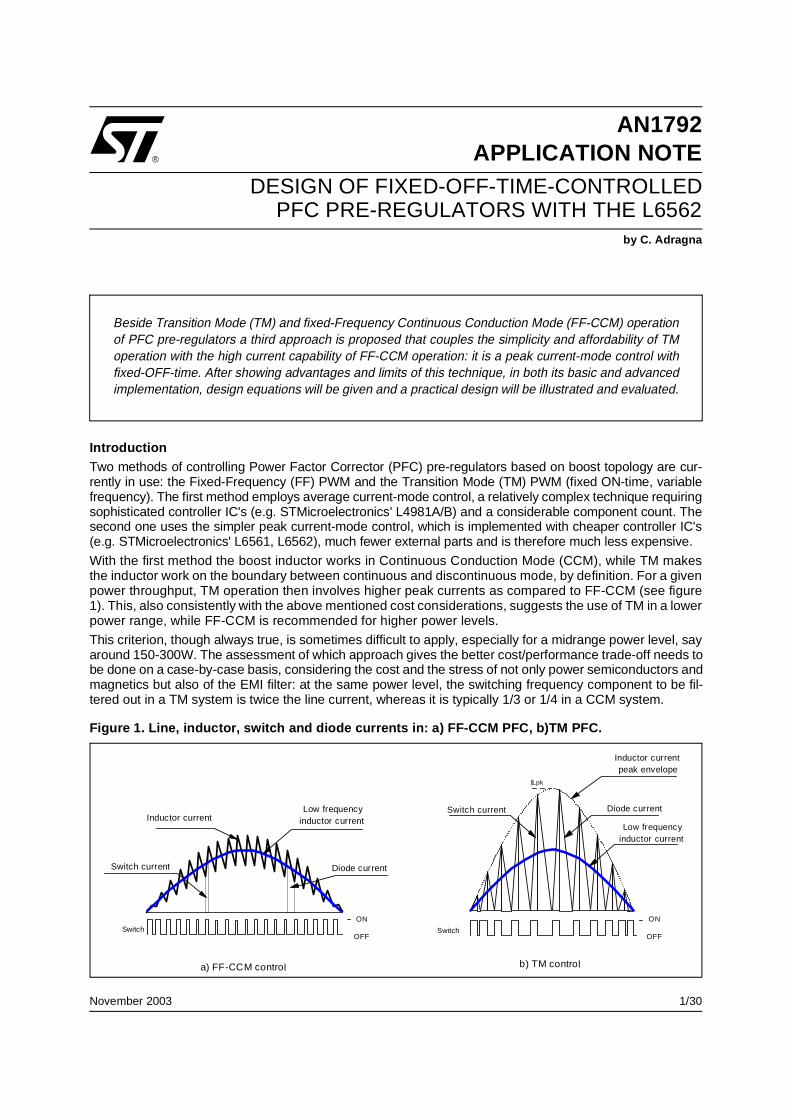
Figure 11. Line current vs. phase angle: a) Full load Pin 0; b) Pin 0/2; c) Pin 0/10
a) c)b)
3
2
1
88
2640
π
Vin
fsw(θ)fsw0
3
2
1
88
264Vin
fsw(θ)fsw0
3
2
1
88
264Vin
fsw(θ)fsw0
θ0
πθ
0
πθ
a) c)b)
3
2
1
88
2640
π
Vin
fsw(θ)fsw0
fsw(θ)fsw0
3
2
1
88
264Vin
fsw(θ)fsw0
fsw(θ)fsw0
3
2
1
88
264Vin
fsw(θ)fsw0
fsw(θ)fsw0
θ0
πθ
0
πθ
6
4
2
88
264
Vin
TON (θ)TOFF
4
3
2
1
88
264
Vin
TON (θ)TOFF
2
1
88
264
Vin
TON (θ)TOFF
a) c)b)
0π
θ0
πθ 0
πθ
6
4
2
88
264
Vin
TON (θ)TOFF
TON (θ)TOFF
4
3
2
1
88
264
Vin
TON (θ)TOFF
TON (θ)TOFF
2
1
88
264
Vin
TON (θ)TOFF
TON (θ)TOFF
a) c)b)
0π
θ0
πθ 0
πθ
1
0.8
0.6
0.4
0.2
088
264
Vin
DL (θ)
88
264
Vin
88
264
Vin
1
0.8
0.6
0.4
DL (θ)
1
0.8
0.6
0.4
0.2
a) c)b)
0π
θ0
πθ
0π
θ
DL (θ)1
0.8
0.6
0.4
0.2
088
264
Vin
DL (θ)
88
264
Vin
88
264
Vin
1
0.8
0.6
0.4
DL (θ)
1
0.8
0.6
0.4
0.2
a) c)b)
0π
θ0
πθ
0π
θ
DL (θ)
a) c)b)
0.8
0.6
0.4
0.2
088
264
Vin
88
264
Vin
88
264
Vin
0π
θ0
πθ
0π
θ
Iin(θ)ILpk0
0.4
0.3
0.2
0.1
0
Iin(θ)ILpk0
0.08
0.06
0.04
0.02
0
Iin(θ)ILpk0
a) c)b)
0.8
0.6
0.4
0.2
088
264
Vin
88
264
Vin
88
264
Vin
0π
θ0
πθ
0π
θ
Iin(θ)ILpk0
0.4
0.3
0.2
0.1
0
Iin(θ)ILpk0
0.08
0.06
0.04
0.02
0
Iin(θ)ILpk0
a) c)b)
0.8
0.6
0.4
0.2
088
264
Vin
88
264
Vin
88
264
Vin
0π
θ0
πθ
0π
θ
Iin(θ)ILpk0
Iin(θ)ILpk0
0.4
0.3
0.2
0.1
0
Iin(θ)ILpk0
Iin(θ)ILpk0
0.08
0.06
0.04
0.02
0
Iin(θ)ILpk0
Iin(θ)ILpk0

AN1792 APPLICATION NOTE
10/30
Figure 12. Inductor current ripple vs. phase angle: a) Full load Pin 0; b) Pin 0/2; c) Pin 0/10
Figure 13. a) Normalized Inductor peak current; b) Normalized line peak current; c) Transition angle
Figure 14. a) Normalized line RMS current; b) Power Factor; c) Total Harmonic Distortion
The pictures of figure 11 show clearly the distortion of the line waveform, quite limited at low line, moreand more accentuated as the line voltage increases and the output power decreases. This is confirmedby the PF and THD% plots of figure 14.
It is important to evaluate the harmonic content of this current waveform, at least at nominal load, in orderto compare it with the limits envisaged by regulations. The Japanese JEIDA-MITI standard is consideredat low input voltage (100Vac) and the European EN61000-3-2 at high input voltage (230Vac).
To do so, Fourier analysis needs to be done on the waveform Iin(θ). The bar diagrams of figure 15 showthe worst-case harmonic contents of the line current ("odd counterpart" of the average inductor currentshown in figure 11), along with the limits envisaged by the above mentioned norms, showing plenty of mar-gin.
a) c)b)a) c)b)
264
Vin
264
Vin
264
Vin
0π
θ0
πθ 0
πθ
∆IL(θ)ILpk0
∆IL(θ)ILpk0
0.4
0.3
0.2
0.1
088
0.2
0.1
088
0.4
0.3
0.2
0.1
0
∆IL(θ)ILpk0
88
a) c)b)a) c)b)
264
Vin
264
Vin
264
Vin
0π
θ0
πθ 0
πθ
∆IL(θ)ILpk0
∆IL(θ)ILpk0
∆IL(θ)ILpk0
∆IL(θ)ILpk0
0.4
0.3
0.2
0.1
088
0.2
0.1
088
0.4
0.3
0.2
0.1
0
∆IL(θ)ILpk0
∆IL(θ)ILpk0
88
ILpkILpk0
1.0
0.8
0.6
0.4
0.2
88
264 1
0
Vin PinPin0
a) H
90
80
70
60
50
40
30
88
264 1
0
Vin PinPin0
θT (°)
c)b)
88
264
Vin
1
0PinPin0
IpkILpk0
0.8
0.6
0.4
0.2
ILpkILpk0
ILpkILpk0
1.0
0.8
0.6
0.4
0.2
88
264 1
0
Vin PinPin0
PinPin0
a) H
90
80
70
60
50
40
30
88
264 1
0
Vin PinPin0
θT (°)
c)b)
88
264
Vin
1
0PinPin0
PinPin0
IpkILpk0
IpkILpk0
0.8
0.6
0.4
0.2
88
264 1
0
Vin PinPin0
Iin(rms)
Iin(rms)0
1.0
0.8
0.6
0.4
0.2
a)
60
40
20
88
264 1
0
Vin
PinPin0
THD%
c)
1.0
0.95
0.90
88
264 1
0
Vin PinPin0
PF
b)
88
264 1
0
Vin PinPin0
Iin(rms)
Iin(rms)0
1.0
0.8
0.6
0.4
0.2
a)
88
264 1
0
Vin PinPin0
Iin(rms)
Iin(rms)0
1.0
0.8
0.6
0.4
0.2
88
264 1
0
Vin PinPin0
PinPin0
Iin(rms)
Iin(rms)0
1.0
0.8
0.6
0.4
0.2
a)
60
40
20
88
264 1
0
Vin
PinPin0
THD%
c)
60
40
20
88
264 1
0
Vin
PinPin0
PinPin0
THD%
c)
1.0
0.95
0.90
88
264 1
0
Vin PinPin0
PinPin0
PF
b)

11/30
AN1792 APPLICATION NOTE
Figure 15. Harmonics of line currents against the class-D limits of: a) JEIDA-MITI; b) EN61000-3-2.
FOT-CCM PFC small-signal analysis. A small-signal model for any PFC pre-regulator, valid for control, line and load variations at frequenciessufficiently lower than the line frequency (quasi-static approximation), is illustrated in figure 16. This modelis generally applicable, regardless of the control technique used: the control affects the values of the pa-rameters g2, j2 and r2 and not the circuit configuration.The values for FOT control can be determined considering Pout=Pin and expanding the large-signal mod-el given in [3] in a three-dimensional Taylor series to the first order around the operating point.
Figure 16. General low-frequency small-signal PFC model.
After a symbolism change and some algebraic manipulations it is possible to arrive at the following result:
, , ,
where VC is the control voltage (the output of the error amplifier of the L6562, pin #2 COMP), KM the multi-plier gain, KP the divider ratio of R1 and R2 and Rsense the current sense resistor (see figure 3).
KM [dimensionally, 1/V] is actually a function of the operating point (an intentional non-linearity vs. VC isintroduced in the multiplier of the L6562 to partly compensate for the gain changes with the input voltage:in particular, j2 is proportional to k2), but the value specified in the datasheet can be used with good ap-proximation.
Ro is the incremental load resistance. The nature of the load driven by the PFC pre-regulator determinesits value. If the load is of resistive type, Ro coincides with the static resistance value:
3 5 7 9 11 13 15 17 19 21 23 25 27 29 31 33 35 37 39
# Harmonic
Amplitude (% of fundamental)
Vin = 120Vac k = 0.424θT = 31°
JEIDA-MITI class D limit
3 5 7 9 11 13 15 17 19 21 23 25 27 29 31 33 35 37 39
# Harmonic
Amplitude (% of fundamental)
Vin = 264Vac k = 0.933θT = 40°
EN61000-3-2 class D limit
a) b)
g k2^ j v
2 C^ r
2 Co Ro
i2^
PFC pre-regulator output port
g2
∂ i2∂k------- Pin
kVout----------------- kΓ
4-------+= = j2
∂ i2∂Vc----------
k2KMKP
2---------------------- Vout
Rsense----------------------= = 1
r2----–
∂ i2∂Vout----------------- Pin
Vout2
---------------- kΓπVout-----------------–= =

AN1792 APPLICATION NOTE
12/30
.
In the important case of a DC-DC converter, which can be regarded as a constant power load, the low-frequency incremental load resistance is negative:
The control-to-output transfer function is:
,
while the line-to-output transfer function is:
.
In the case of constant power load (PFC stage supplying a cascaded DC-DC converter), unlike TM andFF-CCM systems, where the parallel combination of r2 and Ro tends to an open circuit, thus placing thepole of the transfer functions at the origin, in FOT-CCM systems the combination maintains a finite value:
,
so that the pole is still at a finite frequency that moves with the line voltage:
.
The DC gain of the control-to-output transfer function is:
.
FOT-CCM PFC pre-design considerations.Operating frequency and TOFF selection. When specifying the operating frequency of a FOT-controlledPFC stage, some care must be taken of the resulting minimum ON-time of the power switch TONmin. As itcan be easily derived from table 2, this occurs on the top of the sinusoid at maximum line voltage and itsvalue is:
. (2)
If one wants to ensure the operation described by the large-signal model considered so far over the fullinput voltage range, this value has to be greater than the minimum ON-time that the L6562 is able to han-dle (350 ns max.) plus the MOSFET's turn-on and turn-off delays (assume 150ns total). In wide-rangemains applications this means a minimum value of 6.96µs for TOFF and a maximum operating frequency(i.e. on the top of the sinusoid) at minimum line voltage not greater than 45 kHz, which could be quite alimitation, especially in view of a small-size inductor (see next paragraph). Actually, if the conditionTON>TONmin, with TONmin given by (2), is not met in an area around the top of the sinusoid, there will be atemporary unbalance of the volt·second across the inductor, so that the cycle-by-cycle average inductor
Ro ∂Vout∂ Iout----------------- Vout
Iout------------- Vout
2
Pout----------------= = =
Ro ∂Vout∂ Iout----------------- Pout
Iout2
--------------– Vout2
Pout----------------–= = =
voutvc
------------ j2Ro// r2
1 sCoRo// r2+----------------------------------------⋅=
vout
k------------ g2
Ro// r2
1 sCoRo// r2+----------------------------------------⋅=
Ro// r2πVout
kΓ-----------------=
fp1
2π Ro// r2( )Co--------------------------------------- kΓ
2π2VoutCo
--------------------------------k TOFF
2π2LCo
---------------------- = = =
G0voutvC
------------
s 0=
j2 Ro// r2( )πkKMKP
2Γ----------------------- Vout
2
Rsense-------------------
πkKMKP
2----------------------- VoutL
TOFFRsense-------------------------------------= = = =
TONmin
1 kmax–
kmax----------------------TOFF=

13/30
AN1792 APPLICATION NOTE
current will grow. If the system is designed so that this occurs at high line, where the inductor current isconsiderably lower than its maximum values (less than one half), there is no risk of core saturation.
The most conspicuous consequence will be an increased line current distortion: the energy in excessaround the top of the sinusoid will be balanced by a corresponding reduction across the zero crossings,so that the current waveform will get narrower and more peaked. As a result, at high line the harmoniccontents will be higher than expected. This increased distortion may be still acceptable, provided theclass-D limits of the EN61000-3-2 standards are not exceeded at rated load and Vin=230Vac, as pre-scribed by the standard, with some safety margin. However, a slight modification of the control techniquecan significantly improve this situation (see "An improvement of FOT control" section) and allow compli-ance with the standard over a wider load range.
Ripple current (Kr) selection. The selection of the ripple current is a trade-off between inductor size, easeof EMI filtering and line current distortion. Low values of Kr, which result in low inductor current ripple anda lighter input line filter for EMI compliance, lead also to a lower line current distortion because the CCMregion inside a line half-cycle is extended, hence making the sinusoidal portion of Iin(θ) more and moredominant. On the other hand, however, a low Kr results in a larger inductance L and, in the end, in a largermagnetic core. Typical values for Kr range from 0.25 to 0.40.
Inductor selection. If a ferrite core is to be used, due to the moderate switching frequency, the maximumflux density Bmax will be typically limited by core saturation and not by core losses. This also means thattransformer's power losses will be located mostly in the windings. Referring to commonly used Area-Prod-uct formulae [5], a first-cut estimate of the minimum required core size is:
[cm4] .
This formula accounts also for the tolerance of the current limit threshold of the L6562 (see next section).At a higher operating frequency core losses might be dominant, but usually the losses related to dioderecovery force to select a switching frequency where core losses do not dominate yet. As to core losses,there is no worry about the frequency increase with the line voltage pointed out by figure 8 (there is a factorof three): at high line the inductor ripple, and then the flux swing, becomes very small (typically, 10 timessmaller).
In case the system is operated at a moderate switching frequency, it is worthwhile trying to use ferrousalloy powder toroidal cores like Kool-Mµ from Magnetics or -xx from Micrometals, especially if working withquite low Kr values. Typically, core losses will be higher than in a ferrite core and the resulting total effi-ciency will be not as high as, but in some cases this could be a tolerable penalty.
"Tracking boost" configuration. In some applications it may be advantageous to regulate the output volt-age of the PFC pre-regulator so that it tracks the RMS input voltage rather than at a fixed value like inconventional boost pre-regulators. This approach, commonly referred to as "tracking boost" or "followerboost", brings some benefits, such as reduction of the MOSFET's RMS current and of transformer's size,and some drawbacks, such as increased diode current, increased low-frequency output ripple and requir-ing the downstream converter to accommodate a larger input voltage range.
Basically, the tracking boost approach reduces the range of the parameter k increasing its minimum valuekmin. This stated, the benefit of core size reduction becomes apparent if one looks at the above given APminformula. Also the frequency change is reduced and the limits concerning TONmin for a full FOT operationare pushed upwards.
For instance, if the regulated output voltage @Vin=88Vac is set at 250V (and at 400V @Vin=264Vac), kminwill be 0.498 (instead of 0.311), thus the maximum switching frequency @Vin=88Vac for a full FOT oper-ation can be as high as 70 kHz; @Vin=88Vac the MOSFET current is reduced by 11% and its conductionlosses by about 22%, whereas the DC and RMS diode current are increased by 60% and 27% respective-ly; the 2·fL output ripple will be typically increased by about 60%; the minimum AP required for the inductorcore, for the same Kr and Bmax, is reduced by 50%.
APmin 1861 kminKr–
kminKr----------------------------
Pin0TOFF
Bmax---------------------------⋅
1.31
≈

AN1792 APPLICATION NOTE
14/30
FOT-CCM PFC design procedure.The starting point is the electrical design specification, which we assume is as shown in table 5. Actually,a number of requirements is not directly related to the FOT control technique and will be used exactly likein the design of standard TM or FF-CCM PFC pre-regulators. Of course, in this context special emphasiswill be given only to the points directly related to FOT control.
Table 5. Basic electrical specification of a FOT-CCM PFC stage
Based on this information and on the results presented in the previous sections, the recommended step-by-step design procedure is the following:
1) Calculate the range of k (kmin ÷ kmax) associated to the line voltage range:
, .
2) Calculate the required TOFF from the specification on the switching frequency. If fswmax is specified use:
;
if fswmin is specified use:
;
if fsw(m) (average value within a line half-cycle) is specified use:
.
3) Calculate Pin0=Pout0/η and determine Γ:
.
Parameter Symbol
Line voltage range Vin(RMS)min ÷ Vin(RMS)max
Minimum Line frequency fLmin
Regulated output voltage Vout
Rated output power Pout0
Maximum 2fL output voltage ripple ∆Voutpk-pk
Hold-up time TH
Min./max./mean switching frequency (@Vin=Vin(RMS)min, Pout=Pout0) fswmin/fswmax./fsw(m)
Estimated efficiency ηMax. inductor current ripple-to-peak ratio (@Vin=Vin(RMS)min, Pout=Pout0) Kr (= sin θT)
Ambient temperature range Tambmin÷Tambmax
kmin 2Vin RMS( )min
Vout----------------------------------⋅= kmax 2
Vin RMS( )max
Vout-----------------------------------⋅=
TOFF
kmin
fswmax-----------------=
TOFF Krkmin
fswmin----------------=
TOFF1 Kr+
2----------------
kmin
fsw(m)---------------=
ΓPin0
kminVout-------------------------- 4πKr
2π Kr 4 πkmin+( )–--------------------------------------------------=

15/30
AN1792 APPLICATION NOTE
4) From the value of Γ calculate the required inductance L of the boost inductor:
.
5) Calculate the maximum inductor peak current ILpkmax using the value of Γ found in step 3:
.
6) Determine the maximum sense resistor Rsensemax:
,
and select a resistor value Rsense < Rsensemax. 1.6V is the minimum value of the pulse-by-pulsecurrent limiting threshold on the current sense pin of the L6562. Take into account that the value ofthis threshold can go as high as 1.8V, hence the inductor must not saturate up to a current equal to1.8/Rsense.
7) Calculate the current stress of all components, design the boost inductor with any commonly used pro-cedure, and select the MOSFET and the diode. Use either the output voltage ripple or the hold-up spec-ification, whichever gives the higher capacitance value, to select the output capacitor.
8) Design the bias component around the controller IC (multiplier setpoint and feedback) using the samecriteria given for TM systems [6], just considering the different small-signal model as to the feedbackdesign. Finally design the circuit that sets up FOT control:8a. Select a capacitor C in the hundred pF or few nF. Like in an FF controller, the tolerance of this capacitor and its temperature drift will affect the resulting timing.8b. Select the timing resistor value R from (α):
and pick the closest standard value.
8c. Select the limiting resistor Rs using (β) and the speed-up capacitor Cs using (γ).
A practical FOT-CCM PFC design with the L6562.As an example, a 375W design, e.g. suitable for a 300W ATX12V PSU will be now described following theprocedure previously given. The electrical spec, listed in table 6, is consistent with ATX12V specification.
Table 6. Electrical specification of the design example of a 375W, L6562-based FOT-CCM PFC stage
Parameter Value
Line voltage range 90 to 265 Vac
Minimum Line frequency 47 Hz
Regulated output voltage 400V
Rated output power 375 W
Maximum 2fL output voltage ripple 20V pk-pk
Hold-up time 17 ms
Maximum switching frequency (@Vin=88Vac, Pout=375W) 100 kHz
Estimated efficiency (@Vin=88Vac, Pout=375W) 90%
Max. inductor current ripple-to-peak ratio (@Vin=88Vac, Pout=375W) 40%
Maximum ambient temperature 50 °C
LVout
Γ-------------TOFF=
ILpk max
Pin0
kminVout--------------------------
4π 1 Kr kmin–( )2π Kr 4 πkmin+( )–-------------------------------------------------- Γ
1 Kr kmin–
Kr------------------------------= =
Rsensemax1.6
ILpk max---------------------=
R 0.7TOFF
C--------------=

AN1792 APPLICATION NOTE
16/30
Following the step-by-step procedure:
1) The range of k is:
kmin = 90 / 400 = 0.318; kmax = 265 / 400 = 0.937.
2) The required OFF-time is:
;
the minimum ON-time will be:
,
which is shorter than the minimum ON-time handled by the L6562, hence significant additional dis-tortion of the line current is expected at high line.
3) The expected maximum input power is:
Pin0 = 375/0.9 = 417 W,
and Γ is:
[A].
4) The required inductance L of the boost inductor is:
that will be rounded up to 330 µH. Using the same value of Kr will give a small additional margin.
5) The maximum inductor peak current is calculated:
.
6) The maximum sense resistor Rsensemax is:
;
it will be realized with four 0.68Ω, 1W-rated paralleled resistors, for a total resistance of 0.17Ω. Theinductor peak current that the inductor must be able to carry without saturating will be:
.
7) From the formulae in table 4, the MOSFET RMS current is:
;
the diode RMS current is:
2 2
TOFF0.318
100 103⋅
------------------------ 3.18µs= =
TONmin 3.18 106– 1 0.937–
0.937------------------------⋅ 0.21µs= =
Γ 4170.318 400⋅----------------------------- 4 π 0.4⋅ ⋅
2 π 0.4 4 0.318 π⋅+( )–⋅--------------------------------------------------------------- 3.85= =
L 400 3.1 106–⋅ ⋅
3.85--------------------------------------- 322µH= =
ILpkmax 3.851 0.4 0.318⋅–
0.4-------------------------------------⋅ 8.4A= =
Rsensemax1.68.4-------- 0.19Ω= =
ILpksat1.8
0.17----------- 10.6A= =
IQ rms( )417
0.318 400⋅----------------------------- 2 16 0.318⋅
3 π⋅--------------------------– 3.96A= =

17/30
AN1792 APPLICATION NOTE
;
the dissipation on the sense resistor will be 0.17·3.962=2.7W, which justifies the use of four resistors;the selected MOSFET is the STW26NM50, a 0.12Ω/500V MdmeshTM type from STMicroelectronics,housed in a TO247 package; the selected diode is an STTH8R06, a 8A/600V Turbo 2 Ultrafast re-covery rectifier again from STMicroelectronics, housed in a TO220 package. Both of these must bedissipated to keep their temperature within safe limits.
As for the inductor, assuming a peak flux density Bmax=0.3T, a core with a APmin = 1.91 cm4 is need-ed and an E42 core has been chosen. The complete inductor spec can be found in the electric circuitdiagram in figure 17.
The output capacitor is determined by the hold-up time requirement. Assuming a minimum voltage of300V after the line drop, a minimum of 180 µF is needed and a 220µF/450V capacitor will be used.
8) a) A C=560 pF film capacitor is selected.
b) The timing resistor is:
;
the closest standard value (3.9 kΩ) will be selected.
c) The limiting resistor Rs will be such that:
;
since there is no need to stress the clamp a 2.4 kΩ resistor will be chosen. The maximum speed-up capacitor is:
;
a 330 pF film capacitor will be used.
The electrical schematic is shown in figure 17. A prototype of this circuit has been realized and evaluatedon the bench. Figures 18 and 19 show a series of diagrams illustrating its performance.
Figure 17. 375W FOT-CCM PFC pre-regulator: electrical schematic.
IQ rms( )417
0.318 400⋅----------------------------- 16 0.318⋅
3 π⋅-------------------------- 2.41A= =
R 0.7 3.18 106–⋅
560 1012–⋅
----------------------------- 3975Ω= =
15 5.7– 0.5–
10 103– 5.7
3.9 103–⋅
-------------------------+⋅------------------------------------------------------- 768Ω Rs 3.9 10
6– 10 5.7– 0.5–5.7
-----------------------------------⋅<< 2600Ω= =
Cs 560 1012– 5.7
15 5.7– 0.5–-----------------------------------⋅< 362pF=
T1: core E42*21*15, B2 material2.0 mm air gap on centre leg, main winding inductance 0.33 mHN1: 58 T of 20 x AWG32 (∅ 0.2 mm)N2: 6 turns of AWG32
8
3
B1KBU8M
8 °C/W heat sink
R2A620 kΩ
C10.47 µF
400V
C3
22 µF
25V
FUSE5A/250V
R1A120 kΩ
D11N4148
DZ1
1N5248B
R447 Ω
C410 nF
R8 2.4 kΩ
T1
56
L6562 7
2 1
M1
ST
W2
6N
M5
05
°C
/W h
ea
t sin
k
4
R10A499 kΩ
C9220 µF450 V
Vout = 400VPout = 375 W
-
Vac(88V to 264V)
R7A, B, C,D0.68 Ω
1 W
R116.34 kΩ
+
-
C210nF
D4STTH8R06D
20 °C/W heat sink
R6 6.8 Ω
C51 µF
R1B120 kΩ
R2B620 kΩ
R310 kΩ
D21N4148
D31N4148
R93.9 kΩ
C7560 pF
C6 330 pF
R10B499 kΩ
NTC2.5 Ω +
CX20.33 µF
CX10.1 µF
L36 mH
N1
N2
D51N5406
C8100 nF630 V
R56.8 kΩ
Note : EMI filter not tested for EMC compliance

AN1792 APPLICATION NOTE
18/30
Figure 18. 375W FOT-CCM PFC pre-regulator: evaluation data.
Figure 19. 375W FOT-CCM PFC pre-regulator: conformity to JEIDA-MITI and EN61000-3-2 standards.
Figures 20 to 22 show the line current waveforms under the operating conditions considered in the dia-grams of figure 18 (100%, 50% and 20% of the rated load) at nominal voltage of both US and Europeanmains. Note: the waveforms are taken with an acquisition method that eleminates high frequency ripple,just to show the low frequency component, the "odd counterpart" of the average inductor current.
Figure 23 shows a close image of the line current waveform under two different operating conditions: onthe left (a), the waveform is taken at low line, and one can easily recognize the shape as well as the DCMand the CCM portions as per the theory; on the right (b), the waveform, taken at high line, clearly showsthe distortion due to the condition TON>TONmin, with TONmin given by (2), not met throughout a line cycle.Note that in the portion where this occurs, the system is running at a fixed frequency fsw= 1/(TONmin+TOFF).The theoretical current, which assumes it is always TON>TONmin and does not exhibit additional distortion,is shown in red.
(*) Burst-mode operation
50 100 150 200 250 3000.6
0.7
0.8
0.9
1
Vin [Vac]
PF
Pout = 375W
Pout = 180W
Pout=70W
(*) Burst-mode operation
50 100 150 200 250 300392
392.5
393
393.5
394
394.5
395
Vin [Vac]
Vout [Vdc]
Pout = 375W
Pout = 180W
Pout=70W
(*)
(*)
(*)
(*) Burst-mode operation
50 100 150 200 250 30092
93
94
95
96
97
Vin [Vac]
Eff. [%]
Pout = 375W
Pout = 180W
Pout=70W
(*)
(*) Burst-mode operation
50 100 150 200 250 3000
20
40
60
80
Vin [Vac]
THD [%]
Pout = 375W
Pout=180W
Pout = 70W
Vin = 100 Vac, 50 Hz; Pout = 375 W THD = 9.2% PF = 0.996
1 3 5 7 9 11 13 15 17 19 21 23 25 27 29 31 33 35 37 390.0001
0.001
0.01
0.1
1
10
Harmonic Order [n]
Harmonic Current [A]
Measurement JEIDA-MITI class D limits
Vin = 230 Vac, 50 Hz; Pout = 375 W THD = 28.9% PF = 0.957
1 3 5 7 9 11 13 15 17 19 21 23 25 27 29 31 33 35 37 390.001
0.003
0.01
0.03
0.1
0.3
1
3
10
Harmonic Order [n]
Harmonic Current [A]
Measurement EN61000-3-2 class D limits

19/30
AN1792 APPLICATION NOTE
Figure 20. 375W FOT-CCM PFC pre-regulator: line current waveforms @ Pout=375W.
Figure 21. 375W FOT-CCM PFC pre-regulator: line current waveforms @ Pout=180W.
Figure 22. 375W FOT-CCM PFC pre-regulator: line current waveforms @ Pout=70W.
Ch1: Input voltage (after the bridge rectifier)Ch2: Line current (@Vin=115Vac, Pout=375W)
Ch1: Input voltage (after the bridge rectifier)Ch2: Line current (@Vin=230Vac, Pout=375W)
Ch1: Input voltage (after the bridge rectifier)Ch2: Line current (@Vin=115Vac, Pout=180W)
Ch1: Input voltage (after the bridge rectifier)Ch2: Line current (@Vin=230Vac, Pout=180W)
Ch1: Input voltage (after the bridge rectifier)Ch2: Line current (@Vin=115Vac, Pout=70W)
Ch1: Input voltage (after the bridge rectifier)Ch2: Line current (@Vin=230Vac, Pout=70W)

AN1792 APPLICATION NOTE
20/30
Figure 23. Line current: a) at low line; b) at high line, with the additional distortion due to violation of the condition T ON>TONmin for some part of the line cycle (in red the theoretical curve).
An improvement of FOT controlThe most severe limitation of FOT control seems to be the trade-off between operating frequency and dis-tortion of the line current waveform pointed out in the "Operating frequency and TOFF selection" sub-sec-tion. As a matter of fact, if TOFF is selected for an operating frequency above 60-70 kHz on the top of thesinusoid at minimum line voltage, the harmonics of the line current may exceed the class-D limits ofEN61000-3-2 at maximum line voltage (264Vac). Actually the standard prescribes the measurement ofthe harmonic current emissions to be done at the nominal voltage (230 Vac) and rated load but sometimesthe PSU is specified to stay within the limits under a range of operating conditions, e.g. throughout theinput voltage range and/or from rated load down to a minimum value. In this case a trade-off could be dif-ficult or even impossible to find.
A simple modification of the standard Fixed-Off-Time technique can overcome this possible issue. Theidea behind is to make TOFF a function of the line voltage, so that at high line it is long enough to ensurethat the condition TON>TONmin, with TONmin given by (2), is met throughout the entire line cycle. Probablythe simplest way to do so is shown in figure 24a, where TOFF is made a function of the instantaneous linevoltage. The circuit of figure 24b makes TOFF a function of the RMS line voltage thanks to the peak-holdingeffect of T1 (which acts as a buffer) along with Ra and Ca whose time constant is significantly longer thana line half cycle. In the following, reference will be made only to the circuit of figure 24a.
With the addition of R2 and T, as long as the voltage on the ZCD pin during TOFF is above VMULT+VBE, Cis discharged through R1 and R2, following the law:
;
as VZCD(t) falls below VMULT+VBE, T is cut off and C is discharged through R1 only, so that its evolutionfrom that point on is described by:
.
a) b)
DCM DCMCCM CCMCCM
Vin=115VacPout=180W
CC
MDCM
CC
M
CC
M
DCM
CC
M
CCMFF
T <T
ON
O
Nm
in
Vin=230VacPout=375W
VZCD t( ) VZCDclampR1
R1 R2+---------------------- VMULT VBE+( )– e
tR1//R2( )C
-----------------------------–R1
R1 R2+---------------------- VMULT VBE+( )+=
VZCD t( ) R1R1 R2+---------------------- VMULT VBE+( )e
tR1C------------–
=

21/30
AN1792 APPLICATION NOTE
Figure 24. Improved FOT control; T OFF changes with: a) the instantaneous, b) the RMS line voltage.
In this way, once fixed the multiplier operating point (that is, the VMULT /Vin ratio), with a proper selectionof R1 and R2 it is possible to increase TOFF with the line voltage so that at maximum line voltage it is al-ways TON>TONmin. It is easy to see that TOFF is now a function of the instantaneous line voltage. We willrefer to this technique as "Line-modulated Fixed-Off-Time" (LM-FOT).
This modification, though simple, introduces profound changes in the timing relationships, with a positiveinfluence on the energetic relationships. From the control point of view, modulating TOFF is a feedforwardterm that modifies the gain but does not change its characteristics. Then all of the properties of the stan-dard FOT control are maintained.
Due to the highly non-linear nature of the TOFF modulation introduced by T and R2, its effects will be dis-cussed only qualitatively and the quantitative aspects will be provided graphically for a specific case.
Figure 25a shows the dependence of TOFF upon the time constant τ = (R1//R2)·C, TOFF = K2·τ, for differ-ent values of the (R1, R2) divider ratio K1 = R1/(R1+R2). In this diagram and the following ones, it is as-sumed VBE = 0.55V. As long as it is VMULT+VBE < VZCDtrigger, that is VMULT < 0.85V, there is little effecton TOFF, while the effect becomes considerable for higher values of VMULT. Figure 25b shows how TOFF(normalized to the value on the top of the sinusoid at minimum line voltage) changes along a line half-cycleat minimum and maximum line voltage for the particular case of K1=0.9. The multiplier peak voltage@Vin=88Vac is assumed to be 1V, resulting in TOFF@Vin=264Vac 2.5 times longer.
Figure 25. LM-FOT: a) TOFF modulation with the circuit of fig. 25a; b) T OFF change in a line half-cycle.
Figures 26 to 32 are the analogous of figures 8-14: they refer to the same representative system, with theaddition of TOFF modulation. The value of TOFF on the top of the line voltage sinusoid at minimum mainsis the same as in the system of figures 8-14, so that the switching frequency is the same in that point.Quantities are normalized with the same criteria.
Rs
5
L6562
7
D1N4148
R1 CCs
ZCD
GDM
4CS
Rsense
3MULT
Rectifiedinput voltage
R2
TBC557
Rs
5
L6562
7
D1N4148
R1 CCs
ZCD
GDM
4CS
Rsense
3MULT
Rectifiedinput voltage
R2
T2BC557
8
Vcc
T1BC547
Ra68kΩ
Ca1 µF
a) b)
0 0.5 1 1.5 2 2.5 30
5
10
15
20
V MULT
K1 = R1
R1+ R2
K1=0.8
K1=0.85
K1=0.9
K1=0.95
K2
a)
0 0.52 1.05 1.57 2.09 2.62 3.140
0.5
1
1.5
2
2.5
K1=0.9
θ
TOFFTOFF @88Vac Vin=88Vac
Vin=264Vac
b)

AN1792 APPLICATION NOTE
22/30
At low line the switching frequency dos not change much, however, the noticeable point is that, since TOFFgets shorter next to the line voltage zero-crossings, the CCM portion in a line half cycle is enlarged. Theresult is that peak currents will be lower and all RMS currents will be closer to those of a FF-CCM system.Also line current shape will get closer to a perfect sinusoid, then both PF and THD will improve (see figure32).
At high line the switching frequency, which stays close to the minimum around the top of the sinusoid, is onlyabout 20% higher than that at minimum line (instead of 3 times). Efficiency will definitely benefit from that.Around zero-crossings, the frequency increases about 2.5 times, but the power handled in those regions isnot high, then the erosion on the efficiency improvement will be minimum. The minimum ON-time goes from7.1% to 17.8% of the normalized TOFF value but the CCM portion gets narrower: the THD will improve be-cause it is now easy to have TON>TONmin, hence eliminating the related additional distortion, but the achiev-able value is slightly worse. However, diode reverse recovery-related losses will be further reduced, in favorof efficiency. Line current wave shape changes little. Note that the maximum inductor current ripple changeslittle as well but in a line half-cycle it does not occur on the CCM-DCM boundary any more.
Figure 26. Normalized switching frequency vs. phase angle: a) Full load Pin 0; b) Pin 0/2; c) Pin 0/10
Figure 27. Normalized MOSFET's ON-time vs. phase angle: a) Full load Pin 0; b) Pin 0/2; c) Pin 0/10
Figure 28. Inductor current conduction angle vs. phase angle: a) Full load Pin 0; b) Pin 0/2; c) Pin 0/10
a) c)b)
4
2
88
264 0
πVin
fsw(θ)fsw0
6
4
2
88
264
Vin
fsw (θ)fsw0
3
2
1
88
264
Vin
fsw (θ)fsw0
θ0
π
θ0
π
θ
a) c)b)
4
2
88
264 0
πVin
fsw(θ)fsw0
fsw(θ)fsw0
6
4
2
88
264
Vin
fsw (θ)fsw0
fsw (θ)fsw0
3
2
1
88
264
Vin
fsw (θ)fsw0
fsw (θ)fsw0
θ0
π
θ0
π
θ
6
4
2
88
264
Vin
TON (θ)TOFF
3
2
1
88
264
Vin
TON (θ)TOFF
2
1
88
264
Vin
TON (θ)TOFF
a) c)b)
0
π
θ0
π
θ0
π
θ
6
4
2
88
264
Vin
TON (θ)TOFF
TON (θ)TOFF
3
2
1
88
264
Vin
TON (θ)TOFF
TON (θ)TOFF
2
1
88
264
Vin
TON (θ)TOFF
TON (θ)TOFF
a) c)b)
0
π
θ0
π
θ0
π
θ
1
0.8
0.6
0.4
88
264
Vin
88
264
Vin
88
264
Vin
1
0.8
0.6
0.4
0.2
DL (θ)
0.8
0.6
0.4
0.2
a) c)b)
0
π
θ0
π
θ0
π
θ
DL (θ)DL (θ)
1
0.8
0.6
0.4
88
264
Vin
88
264
Vin
88
264
Vin
1
0.8
0.6
0.4
0.2
DL (θ)
0.8
0.6
0.4
0.2
a) c)b)
0
π
θ0
π
θ0
π
θ
DL (θ)DL (θ)
23/30
AN1792 APPLICATION NOTE
Figure 29. Line current vs. phase angle: a) Full load Pin 0; b) Pin 0/2; c) Pin 0/10
Figure 30. Inductor current ripple vs. phase angle: a) Full load Pin 0; b) Pin 0/2; c) Pin 0/10
Figure 31. a) Normalized Inductor peak current; b) Normalized line peak current; c) Transition angle
Figure 32. a) Normalized line RMS current; b) Power Factor; c) Total Harmonic Distortion
a) c)b)
0.8
0.6
0.4
0.2
088
264
Vin
88
264
Vin
88
264
Vin
0π
θ0
πθ
0π
θ
Iin(θ)ILpk0
0.4
0.3
0.2
0.1
0
Iin(θ)ILpk0
0.08
0.06
0.04
0.02
0
Iin(θ)ILpk0
a) c)b)
0.8
0.6
0.4
0.2
088
264
Vin
88
264
Vin
88
264
Vin
0π
θ0
πθ
0π
θ
Iin(θ)ILpk0
0.4
0.3
0.2
0.1
0
Iin(θ)ILpk0
0.08
0.06
0.04
0.02
0
Iin(θ)ILpk0
a) c)b)a) c)b)
264
Vin
264
Vin
264
Vin
0
π
θ0
π
θ0
π
θ
∆IL(θ)∆IL0
∆IL(θ)∆IL0
88
0.4
0.3
0.2
0.1
088
0.4
0.3
0.2
0.1
088
0.2
0.15
0.1
0.05
0
∆IL(q)∆IL0
a) c)b)a) c)b)
264
Vin
264
Vin
264
Vin
0
π
θ0
π
θ0
π
θ
∆IL(θ)∆IL0
∆IL(θ)∆IL0
88
0.4
0.3
0.2
0.1
088
0.4
0.3
0.2
0.1
088
0.2
0.15
0.1
0.05
0
∆IL(q)∆IL0
∆IL(q)∆IL0
1.0
0.8
0.6
0.4
0.2
88
2641
0VinPinPin0
a) H
90
60
30
088
2641
0
Vin
PinPin0
θT (°)
c)b)
88
264
Vin
1
0PinPin0
Ipk
ILpk0
0.8
0.6
0.4
0.2
ILpk
ILpk0
1.0
0.8
0.6
0.4
0.2
88
2641
0VinPinPin0
PinPin0
a) H
90
60
30
088
2641
0
Vin
PinPin0
PinPin0
θT (°)
c)b)
88
264
Vin
1
0PinPin0
PinPin0
Ipk
ILpk0
Ipk
ILpk0
0.8
0.6
0.4
0.2
ILpk
ILpk0
ILpk
ILpk0
88
264 1
0Vin
PinPin0
Iin(rms)
Iin(rms)0
1.0
0.8
0.6
0.4
0.2
a)
40
20
88
264 1
0
Vin
PinPin0
THD%
c)
1.0
0.95
0.90
88
264 1
0Vin
PinPin0
PF
b)
88
264 1
0Vin
PinPin0
PinPin0
Iin(rms)
Iin(rms)0
Iin(rms)
Iin(rms)0
1.0
0.8
0.6
0.4
0.2
a)
40
20
88
264 1
0
Vin
PinPin0
THD%
c)
1.0
0.95
0.90
88
264 1
0Vin
PinPin0
PinPin0
PF
b)

AN1792 APPLICATION NOTE
24/30
The starting point for the design of the circuit of figure 25a is the pair of the desired values for TOFF on thetop of the line voltage sinusoid at minimum (TOFF@Vin=Vin(RMS)min) and maximum line(TOFF@Vin=Vin(RMS)max). Let ρ their ratio: ρ = TOFF@Vin=Vin(RMS)max / TOFF@Vin=Vin(RMS)min. Withthese data the design can be done with the aid of the diagrams in figure 33. The diagrams, which assumean input voltage range 88-264 Vac, features two sets of curves, ρ curves and K2 curves, each of themplotted for a particular value of the peak multiplier voltage VMULTpk @88Vac.
Figure 33. Diagrams for the design of the circuit of figure 24a (valid for Vacmin=88V, Vacmax=264V).
The suggested step-by-step design procedure is the following:
1) Determine the multiplier setpoint using the same criteria given for TM systems [6] and take note of theresulting VMULTpk @88Vac value. It should be between 0.7 and 1V.
2) Draw an horizontal line located at the desired value of ρ (on the left vertical axis) as long as it interceptsthe curve relevant to the value VMULTpk previously determined in P1. The abscissa of P1 gives the nec-essary value of the parameter K1.
3) From P1 draw a vertical line as long as it intercepts the K2 curve relevant to the same value of VMULTpkin P2. The ordinate of P2 (on the right vertical axis) gives the necessary value of K2.
4) Calculate the time constant τ =(R1//R2) C necessary to achieve the desired TOFF@88Vac:
.
5) Select a capacitor C in the hundred pF or few nF, and determine the required resistance value:
.
6) Determine R1 and R2:
. (23a, b)
7) Select the limiting resistor Rs according to the following inequalities:
,
and the speed-up capacitor Cs using (γ).
The 375W design will now be modified to implement LM-FOT. The target is to keep TOFF = 3.18 µs@90Vac and to get TOFF = 8 µs @265Vac, thereby ρ = 8/3.18 ≈2.5. The input voltage range, althoughdifferent from, is very close to that covered by the diagrams of figure 33, then these curves are still appli-
0.8V
ρ
K1
0.8 0.810.820.830.840.850.860.870.880.89 0.9 0.911.5
2
2.5
3
3.5
4
0.920.930.940.95
2
2.4
2.8
3.2
3.6
4
4.4
4.8
5.2
5.6
6
K2
ρ curves
1.0V
0.9V 0.8V 0.9V 1.0V
K2 curves
P1
P2
V = 0.7MULTpkV = 0.7MULTpk
τTOFF @ 88Vac
K2-----------------------------------------=
R' R1//R2 = τC----=
R1 R'1 K1–-----------------= R2 R'
K1-------=
VGDx VZCDclamp VF––
IZCDx
VZCDclamp
R1-----------------------------+
--------------------------------------------------------------- RsVGD VZCDclamp VF––( )R1R2
VZCDclamp VBE–( )R1 VZCDclampR2+---------------------------------------------------------------------------------------------------------<<

25/30
AN1792 APPLICATION NOTE
cable. Following the above given step-by-step procedure:
1) From the part values in the schematic diagram of figure 17, VMULTpk @90Vac=1.02V, then the curvesfor VMULTpk =1V will be considered.
2) In figure 33 the points P1 and P2 are shown; the resulting values for K1 and K2 are 0.891 and 4.17 re-spectively.
3) The required time constant is:
.
4) The same capacitor (C=560 pF) will be used, then the associated resistance value will be:
.
5) R1 and R2 will be respectively:
;
the standard values R1=12kΩ and R2=1.5kΩ will be chosen.
6) Under the worst-case condition, only R1 will divert some current from the ZCD pin to ground, then thelimiting resistor Rs must be selected according to:
;
in this case a 910Ω resistor will be chosen. Cs will be the same 330 pF capacitor.
The prototype, modified as per the above guidelines, has been evaluated to check the actual differenceswith the former realization. Figures 34 to 38 show a series of diagrams illustrating its performance.
Figure 34. 375W LM-FOT-CCM PFC pre-regulator: evaluation data.
τ 3.18 106–⋅
4.17---------------------------- 0.76 10
6–s⋅= =
R' 0.76 106–⋅
560 1012–⋅
----------------------------- 1357Ω= =
R1 13571 0.891–------------------------ 12450Ω= = R2 1357
0.891--------------- 1523Ω= =
15 5.7– 0.5–
10 103– 5.7
12 103–⋅
-----------------------+⋅----------------------------------------------------- 840Ω Rs
10 5.7– 0.5–( )1.5 10312 10
3⋅⋅
5.7 0.55–( )12 103
5.7 1.5 103⋅ ⋅+⋅
--------------------------------------------------------------------------------------------- 972= Ω<<=
50 100 150 200 250 3000.86
0.88
0.9
0.92
0.94
0.96
0.98
1
Vin [Vac]
PF
Pout = 375W
Pout = 180W
Pout=70W
50 100 150 200 250 3000
10
20
30
40
50
Vin [Vac]
THD [%]
Pout = 375W
Pout=180W
Pout = 70W
50 100 150 200 250 300391
391.5
392
392.5
393
393.5
394
Vin [Vac]
Vout [Vdc]
Pout = 375W
Pout = 180W
Pout=70W
50 100 150 200 250 30092
93
94
95
96
97
98
Vin [Vac]
Eff. [%]
Pout = 375W
Pout = 180W
Pout=70W
AN1792 APPLICATION NOTE
26/30
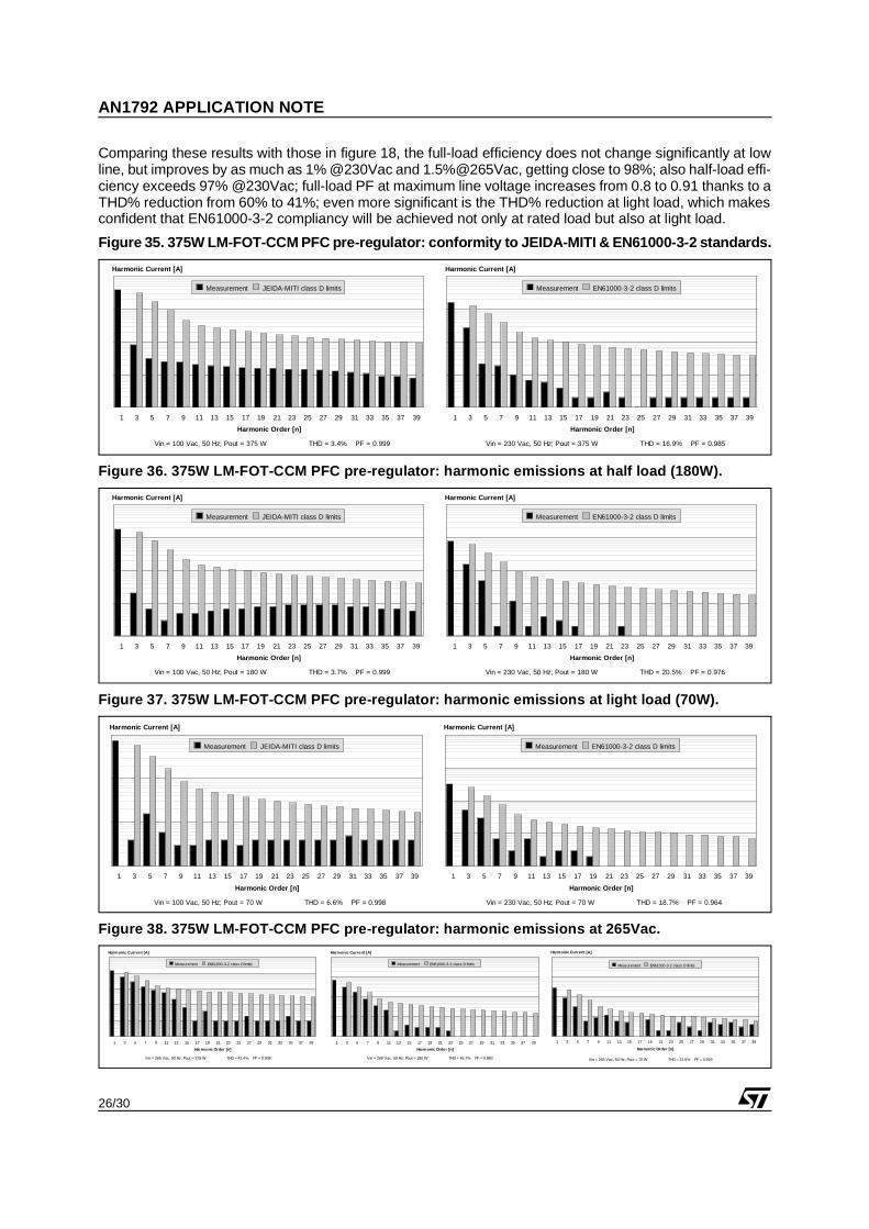
Comparing these results with those in figure 18, the full-load efficiency does not change significantly at lowline, but improves by as much as 1% @230Vac and 1.5%@265Vac, getting close to 98%; also half-load effi-ciency exceeds 97% @230Vac; full-load PF at maximum line voltage increases from 0.8 to 0.91 thanks to aTHD% reduction from 60% to 41%; even more significant is the THD% reduction at light load, which makesconfident that EN61000-3-2 compliancy will be achieved not only at rated load but also at light load.
Figure 35. 375W LM-FOT-CCM PFC pre-regulator: conformity to JEIDA-MITI & EN61000-3-2 standards.
Figure 36. 375W LM-FOT-CCM PFC pre-regulator: harmonic emissions at half load (180W).
Figure 37. 375W LM-FOT-CCM PFC pre-regulator: harmonic emissions at light load (70W).
Figure 38. 375W LM-FOT-CCM PFC pre-regulator: harmonic emissions at 265Vac.
1 3 5 7 9 11 13 15 17 19 21 23 25 27 29 31 33 35 37 39
Harmonic Order [n]
Harmonic Current [A]
Measurement JEIDA-MITI class D limits
Vin = 100 Vac, 50 Hz; Pout = 375 W THD = 3.4% PF = 0.999
1 3 5 7 9 11 13 15 17 19 21 23 25 27 29 31 33 35 37 39
Harmonic Order [n]
Harmonic Current [A]
Measurement EN61000-3-2 class D limits
Vin = 230 Vac, 50 Hz; Pout = 375 W THD = 16.9% PF = 0.985
1 3 5 7 9 11 13 15 17 19 21 23 25 27 29 31 33 35 37 39
Harmonic Order [n]
Harmonic Current [A]
Measurement JEIDA-MITI class D limits
Vin = 100 Vac, 50 Hz; Pout = 180 W THD = 3.7% PF = 0.999
1 3 5 7 9 11 13 15 17 19 21 23 25 27 29 31 33 35 37 39
Harmonic Order [n]
Harmonic Current [A]
Measurement EN61000-3-2 class D limits
Vin = 230 Vac, 50 Hz; Pout = 180 W THD = 20.5% PF = 0.976
1 3 5 7 9 11 13 15 17 19 21 23 25 27 29 31 33 35 37 39
Harmonic Order [n]
Harmonic Current [A]
Measurement JEIDA-MITI class D limits
Vin = 100 Vac, 50 Hz; Pout = 70 W THD = 6.6% PF = 0.998
1 3 5 7 9 11 13 15 17 19 21 23 25 27 29 31 33 35 37 39
Harmonic Order [n]
Harmonic Current [A]
Measurement EN61000-3-2 class D limits
Vin = 230 Vac, 50 Hz; Pout = 70 W THD = 18.7% PF = 0.964
1 3 5 7 9 11 13 15 17 19 21 23 25 27 29 31 33 35 37 39
Harmonic Order [n]
Harmonic Current [A]
Measurement EN61000-3-2 class D limits
Vin = 265 Vac, 50 Hz; Pout = 375 W THD = 41.4% PF = 0.908
1 3 5 7 9 11 13 15 17 19 21 23 25 27 29 31 33 35 37 39
Harmonic Order [n]
Harmonic Current [A]
Measurement EN61000-3-2 class D limits
Vin = 265 Vac, 50 Hz; Pout = 180 W THD = 45.7% PF = 0.883
1 3 5 7 9 11 13 15 17 19 21 23 25 27 29 31 33 35 37 39
Harmonic Order [n]
Harmonic Current [A]
Measurement EN61000-3-2 class D limits
Vin = 265 Vac, 50 Hz; Pout = 70 W THD = 31.6% PF = 0.919

27/30
AN1792 APPLICATION NOTE
As to this point, the harmonic analysis shown in figures 35 to 38 confirms that. In particular, figure 38shows that the emissions are within the limits even at light load and maximum line voltage. From the totaldistortion point of view, half-load seems to be the worst-case condition.
Figure 39. 375W LM-FOT-CCM PFC pre-regulator: line current waveforms @ Pout=375W.
Figure 40. 375W LM-FOT-CCM PFC pre-regulator: line current waveforms @ Pout=180W.
Figure 41. 375W LM-FOT-CCM PFC pre-regulator: line current waveforms @ Pout=70W.
Ch1: Input voltage (after the bridge rectifier)Ch2: Line current (@Vin=115Vac, Pout=375W)
Ch1: Input voltage (after the bridge rectifier)Ch2: Line current (@Vin=230Vac, Pout=375W)
Ch1: Input voltage (after the bridge rectifier)Ch2: Line current (@Vin=115Vac, Pout=180W)
Ch1: Input voltage (after the bridge rectifier)Ch2: Line current (@Vin=230Vac, Pout=180W)
Ch1: Input voltage (after the bridge rectifier)Ch2: Line current (@Vin=115Vac, Pout=70W)
Ch1: Input voltage (after the bridge rectifier)Ch2: Line current (@Vin=230Vac, Pout=70W)

AN1792 APPLICATION NOTE
28/30
Figures 39 to 41 show the line current waveforms under the operating conditions considered in the dia-grams of figure 34 (100%, 50% and 20% of the rated load) at nominal voltage of both US and Europeanmains. It is interesting to compare these waveforms with those in figures 20 to 22. The effect of the linemodulation of TOFF is conspicuous.
Figure 42. Line current a) nearly sinusoidal at low line; b) without additional distortion at high line.
This effect is clearly pointed out in figure 42 as well. It shows a close image of the line current waveformunder the same two operating conditions as in figure 23. On the left (a), the waveform is taken at low line,half-load and one can easily recognize that it is very close to a sinusoid (its THD is 3.8%); this result iseven better than the theoretical prediction because the theoretical CCM-DCM boundary falls in a regionwhere the effect of the THD optimizer circuit of the L6562 becomes apparent (TON is forced to be longerthan the value commanded by the control loop). As a consequence, in that region the peak inductor cur-rent is higher and the actual CCM-DCM boundary is virtually located at or extremely close to zero-cross-ings.
On the right (b), the waveform is taken at high line, full-load and in this case the waveform closely followsthe theoretical one, unlike that in figure 23b, thus proving the effectiveness of a longer TOFF.
Considering that at low line the system works almost entirely in CCM, so that the line current looks verymuch like that of a FF-CCM system, it is possible to face the design of the power stage with the same ap-proach used in an FF-CCM type. The significant difference is the point where inductor current ripple ampli-tude is maximum: whereas it is well-defined with FF-CCM, it is not with LM-FOT and it is not possible tofind a simple design formula that relates the inductance value L to the maximum desired ripple. As a ruleof thumb, it is possible to refer to the ripple amplitude on the top of the sinusoid at minimum line voltageand determine L so that the ripple amplitude is 75% of the maximum desired.
This stated, the recommended step-by-step design procedure of an LM-FOT-controlled PFC is the following:
1) Calculate the range of k (kmin ÷ kmax) associated to the line voltage range:
, .
2) Calculate the required TOFFmin from the specification on the maximum switching frequency (on the topof the line voltage sinusoid) fswmax at minimum line voltage:
.
a) b)
Vin=115VacPout=180W
DCM DCMCCM CCMCCM
Vin=230VacPout=375W
kmin 2Vin RMS( )min
Vout----------------------------------= kmax 2
Vin RMS( )max
Vout-----------------------------------=
TOFFmin
kmin
fsw max-------------------=

29/30
AN1792 APPLICATION NOTE
3) Calculate Pin0=Pout0/η and determine the maximum line peak current Ipk:
.
4) Determine the ripple amplitude on the top of the sinusoid at minimum line voltage, assuming it is 75% ofthe maximum specified, related to Kr:
.
5) Determine the required inductance L of the boost inductor:
.
6) Calculate ILpkmax:
.
7) Determine the maximum sense resistor Rsensemax:
and select a resistor value Rsense < Rsensemax. 1.6V is the minimum value of the pulse-by-pulsecurrent limiting threshold on the current sense pin of the L6562. Take into account that the value ofthis threshold can go as high as 1.8V, hence the inductor must not saturate up to a current equal to1.8/Rsense.
8) Calculate the current stress of all components, design the boost inductor with any commonly used pro-cedure, and select the MOSFET and the diode. Use either the output voltage ripple or the hold-up spec-ification, whichever gives the higher capacitance value, to select the output capacitor.
9) Design the bias component around the controller IC (multiplier setpoint and feedback) using the samecriteria given for TM systems [6], just considering the different small-signal model as to the feedback de-sign. Finally, once specified TOFF@Vin=Vin(RMS)max > 7 µs, design the circuit that sets up LM-FOT con-trol according to the given procedure.
ConclusionsFixed-Off-Time control of PFC pre-regulators has been discussed and analyzed, highlighting its meritsand drawbacks. Simplified large-signal and small-signal models have been described and a design pro-cedure has been provided for its basic implementation. A prototype built following this procedure and uti-lizing the L6562, a cheap 8-pin Transition-Mode controller IC with some simple additions, has beenevaluated on the bench and the results have been presented.
An improved version, denominated "Line-modulated Fixed-Off-Time" (LM-FOT) control, has been intro-duced and its benefits over the basic FOT control have been shown and proven by the bench evaluationof the prototype modified accordingly. In particular, from these results it is possible to conclude that an LM-FOT-controlled PFC pre-regulator, operated in CCM, at low line performs exactly like a conventional FF-CCM type. Thereby, the power stage can be designed with the same procedure and using the same rela-tionships.
The good performance that the system has shown, especially in the improved LM version, validates thisapproach, which couples the simplicity and cost-effectiveness of TM operation with the high-current capa-bility of CCM operation. FOT control can justifiably be added to these two popular techniques.
lpkmax
2Pin0
kminVout--------------------------=
ILpk∆ 6Kr8 3Kr–------------------- lpkmax
12Kr8 3Kr–-------------------
Pin0
kminVout--------------------------= =
L 1 kmin–( )VoutILpk∆
--------------TOFFmin8 3Kr–12Kr
-------------------Vout2
Pin0----------------kmin 1 kmin–( )TOFFmin= =
ILpkmax lpkmax12--- ILpk∆+
88 3Kr–------------------- lpkmax
168 3Kr–-------------------
Pin0
kminVout--------------------------= = =
Rsensemax1.6
lPkmax-----------------=

Information furnished is believed to be accurate and reliable. However, STMicroelectronics assumes no responsibility for the consequencesof use of such information nor for any infringement of patents or other rights of third parties which may result from its use. No license is grantedby implication or otherwise under any patent or patent rights of STMicroelectronics. Specifications mentioned in this publication are subjectto change without notice. This publication supersedes and replaces all information previously supplied. STMicroelectronics products are notauthorized for use as critical components in life support devices or systems without express written approval of STMicroelectronics.
The ST logo is a registered trademark of STMicroelectronics.All other names are the property of their respective owners
© 2003 STMicroelectronics - All rights reserved
STMicroelectronics GROUP OF COMPANIESAustralia - Belgium - Brazil - Canada - China - Czech Republic - Finland - France - Germany - Hong Kong - India - Israel - Italy - Japan -
Malaysia - Malta - Morocco - Singapore - Spain - Sweden - Switzerland - United Kingdom - United Stateswww.st.com
30/30
AN1792 APPLICATION NOTE
REFERENCES[1] R. B. Ridley "A New Continuous-Time Model for Current-Mode Control with Constant Frequency,
Constant On-Time and Constant Off-Time, in CCM and DCM", IEEE Power Electronics SpecialistsConference Record, San Antonio, Texas, pp. 382-389, 1990.
[2] D. H. Venable "Current Mode Control", Venable Technical Paper #5, www.venableind.com[3] C. Adragna "Fixed-Off-Time Control of PFC Pre-regulators", 10th European Conference on Power
Electronics and Applications, EPE2003, Toulouse, France, paper 382.
[4] "L6562, Transition-Mode PFC Controller", Datasheet, www.st.com
[5] Lloyd H. Dixon, Jr. "Filter Inductor and Flyback Transformer Design for Switching Power Supplies",UNITRODE Power Supply Design Seminar Manual, 1994 (SEM-1000)
[6] "L6561, Enhanced Transition Mode Power Factor Corrector", AN966, www.st.com