Embed Size (px)
Citation preview
Interfacing the X9408, X9418 XDCP to 8051 Microcontrollers
APPLICATION NOTE
AN1144Rev 0.00
Jun 20, 2005
This application note describes the routines for the control of an X9408 or X9418 digitally controllable potentiometer. The X9408, X9418 devices have a variety of different instructions that provide flexibility to the designer. Additionally, the nonvolatile nature of the device allows for stored wiper positions that can be retrieved after power cycles.
The following code implements all of the available X9408, X9418 instructions using a standard bi-directional bus protocol. Although the subroutines occupy about 300 bytes of program memory, designers who won't need to implement all of the instructions can shorten the code by removing any unnecessary routines. However, this will necessitate the reassembly of the code.
For those instructions which program the nonvolatile data registers (XFR_WCR, GXFR_WCR, & WRITE_DR), acknowledge polling has been implemented to determine an early completion of the internal write cycle. Although this is automatically handled by the routines, a word or two regarding the procedure should be informative. After issuing a start condition, the master sends a slave address and receives an acknowledge. It then issues an instruction byte to the X9408, X9418 and again receives an acknowledge. If necessary, it now transmits the data byte and receives a final acknowledge. The master must then initiate a stop condition which will cause the X9408, X9418 to begin an internal write cycle. The X9408, X9418 pins go to high impedance until this internal cycle is complete. The master can now begin
acknowledge polling by successively sending start conditions followed by "dummy" instructions. When the X9408, X9418 finally answers with an acknowledge, the internal write cycle has been completed. The master must then initiate a stop condition. After the next start condition, the X9408, X9418 is ready to receive further instructions.
In the code listing, an assumption was made that the code executes upon a reset of the microcontroller. That is, the code is loaded into low memory, however this can be changed with an ORG assembler directive. Simple MAIN program routines are included in the code listing. These can be modified for different device addresses, different registers and different DCPs within the device.
In this listing, the commands cause an X9408, X9418 (at A3A2A1A0 = 1100 to be accessed.) The listing also includes some instructions that are specific to the Cygnal 80C51 processor. These should be examined and modified, as needed, for the specific 80C51 in the system. The commands issued in the “Main” section of the code are simple assignment and call sequences.
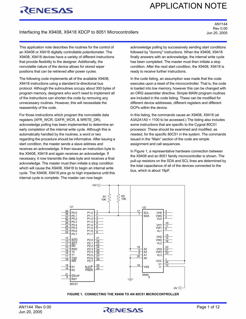
In Figure 1, a representative hardware connection between the X9408 and an 8051 family microcontroller is shown. The pull-up resistors on the SDA and SCL lines are determined by the total capacitance of all of the devices connected to the bus, which is about 18pF.
+5V
-5V
U1
80C51
2122232425262728
17
16
2930
11
10
31
1918
9
3938373635343332
12345678
1213
1415
P2.0P2.1P2.2P2.3P2.4P2.5P2.6P2.7
RD
WR
PSENALE/P
TXD
RXD
EA/VP
X1X2
RST
P0.0P0.1P0.2P0.3P0.4P0.5P0.6P0.7
P1.0P1.1P1.2P1.3P1.4P1.5P1.6P1.7
INT0INT1
T0T1
U2
X9408
19
151416
222123
124
177
1858
20
342
10119
13VSS
VH2VW2VL2
VH3VW3VL3
VCCV+
SCLSDA
A3A2A1A0
VH0VW0VL0
VH1VW1VL1
V-
R110K
R210K
FIGURE 1. CONNECTING THE X9408 TO AN 80C51 MICROCONTROLLER
AN1144 Rev 0.00 Page 1 of 12Jun 20, 2005

Interfacing the X9408, X9418 XDCP to 8051 Microcontrollers
80C51 MICROCONTROLLER ROUTINES FOR MANIPULATING AN X9408;-----------------------------------------------------------------------------; ; 80C51 MICROCONTROLLER ROUTINES FOR MANIPULATING AN X9408; QUAD EEPOT; ; (C) INTERSIL INC. 2002 ; CEM ;; FILE NAME : X9408_8051.TXT ; TARGET MCU: Cygnal C8051F000 ; DESCRIPTION:; ; This code provides basic 80C51 code for commmunicating with and; controlling the X9408 quad digital potentiometer. In this listing; is code that implements all of the available X9408 instructions. ; The X9408 communicates via a 2-wire bus that is similar, but a little ; different from the I2C bus. This code is very generic and can be; simplified and shortened by removing any unnecessary routines.;; For those instructions which program the nonvolatile data registers; (XFR_WCR, GFXR_WCR, and WRITE_DR) this program provides acknowledge; polling to determine early completion of the internal write cycle. ; Although this is handled automatically by the routines, some background; might be helpful.;; After issuing a start condition, the master sends a slave address; and receives and acknowledge (ACK). The master then sends an instruction; byte to the X9408 and again receives an ACK. If necessary, the master sends; a data byte and receives a final ACK. The master then initiates a stop; condition to signal the X9408 to begin an internal nonvolatile write; cycle. When the write cycle begins, the I/O pins go to a high impedance state; and remain in this state until the nonvolatile write is complete.;; Immediately following the stop condition, the master can begin acknowledge; polling by successively sending start conditions, followed by "dummy" ; instructions. When the X9408 finally answers with an acknowledge, the ; internal write cycle is completed. The master then issues a stop; condition. After the next start condition, the X9408 is ready to receive; further instructions.;; This code give the flexibility to communicate with up to 16 different X9408; devices on the same bus. It does this by using a register, named "ADDR_BYTE".; This register is loaded with the specific slave address and address of the; desired X9408 device. The register can be saved if there is only one X9408; on the bus, by making ADDR_BYTE a constant.;; An 80C51 register is used to identify the particular X9408 register or DCP, or both,; are used for a particular operation. There are various constants available for; easy selection of the WCR and DR combination. The contents of the register; is appended to the specific instruction in the "instr_gen' routine. ;; A register is used as a counter for keeping track of the number of bits sent; in each byte.
; A register is used for the increment/decrement instruction to specify up or; down movement of the wiper. For each command, the master loads the "PULSES" ; register with a direction bit and 6 bits of count. If the MSB is a 1; the wiper increments the specified number of tap positions. If the MSB ; is a 0 the wiper decrements the specified number of tap positions.;; A register is used to hold the specific command being executed. This allows ; the instruction to be built up and sent to the X9408.;; In the MAIN section are sample main code segments showing how to use the ; various subroutines. ;; This code was tested on a Cygnal 80C51 microcontroller, using the Cygnal; tools. The specific routines required to set up the Cygnal processor
AN1144 Rev 0.00 Page 2 of 12Jun 20, 2005

Interfacing the X9408, X9418 XDCP to 8051 Microcontrollers
; are identified and are probably not needed for other standard 8051 devices.; Since each 8051 may have specific requirements that are not handled in this; code, the programmer is advised to check the setup needs of the specific; 80C51 derivation that is being used.;;-----------------------------------------------------------------------------; I/O Definition;-----------------------------------------------------------------------------
SCL bit p1.0 ; 80C51 pin used AS SCLSDA bit p1.1 ; 80C51 pin used AS SDA
;-----------------------------------------------------------------------------; Register Definition;-----------------------------------------------------------------------------
$include (c8051f000.inc); Include regsiter definition file (Cygnal). TEMP equ r1 ; Scratch registerCOUNT equ r2 ; Loop counting registerPULSES equ r3 ; Bits -> DIR 0 ###### (#=pulses = 0 to 64)COMMAND equ r4 ; Instruction (I.E. 0,4,8,12,16,...)ID equ r5 ; Bits -> 0 0 0 0 R1 R0 P1 P0ADDR_BYTE equ r6 ; Bits -> 0 1 0 1 A3 A2 A1 A0DATA_BYTE equ r7 ; Bits -> CM DW D5 D4 D3 D2 D1 D0
;-----------------------------------------------------------------------------; Constant Definition;-----------------------------------------------------------------------------
SLAVE_ADR0 equ 050hSLAVE_ADR1 equ 051hSLAVE_ADR2 equ 052hSLAVE_ADR3 equ 053hSLAVE_ADR4 equ 054hSLAVE_ADR5 equ 055hSLAVE_ADR6 equ 056hSLAVE_ADR7 equ 057hSLAVE_ADR8 equ 058hSLAVE_ADR9 equ 059hSLAVE_ADR10 equ 05AhSLAVE_ADR11 equ 05BhSLAVE_ADR12 equ 05ChSLAVE_ADR13 equ 05DhSLAVE_ADR14 equ 05EhSLAVE_ADR15 equ 05Fh;WCR_0 equ 00hWCR_1 equ 01hWCR_2 equ 02hWCR_3 equ 03h;DR_0 equ 00hDR_1 equ 04hDR_2 equ 08hDR_3 equ 0Ch;DCP0_R0 equ 00hDCP0_R1 equ 04hDCP0_R2 equ 08hDCP0_R3 equ 0Ch;DCP1_R0 equ 01hDCP1_R1 equ 05hDCP1_R2 equ 09hDCP1_R3 equ 0Dh;DCP2_R0 equ 02hDCP2_R1 equ 06hDCP2_R2 equ 0Ah
AN1144 Rev 0.00 Page 3 of 12Jun 20, 2005

Interfacing the X9408, X9418 XDCP to 8051 Microcontrollers
DCP2_R3 equ 0Eh;DCP3_R0 equ 03hDCP3_R1 equ 07hDCP3_R2 equ 0BhDCP3_R3 equ 0Fh;
READWCR equ 0WRITEWCR equ 4READDR equ 8WRITEDR equ 12XFRDR equ 16XFRWCR equ 20GXFRDR equ 24GXFRWCR equ 28INCDECWIPER equ 32
;-----------------------------------------------------------------------------; INTERNAL RAM;-----------------------------------------------------------------------------
STACK_TOP equ 060H ; Stack top
;-----------------------------------------------------------------------------; RESET and INTERRUPT VECTORS;-----------------------------------------------------------------------------
cseg AT 0 ljmp main ; Locate a jump to the start of code at
;-----------------------------------------------------------------------------; CODE SEGMENT;-----------------------------------------------------------------------------
Code_Seg segment CODE
rseg Code_Seg Switch to this code segment. using Specify register bank for the following program code.
;-----------------------------------------------------------------------------;; NAME: execute ; FUNCTION: Determines which X9408 instruction is issued,; then executes; INPUTS: COMMAND ; OUTPUTS: none; CALLS: read_wcr, read_dr, write_wcr, write_dr, xfr_dr,; xfr_wcr, gxfr_dr, gxfr_wcr, inc_wiper ; AFFECTED: DPTR, A ; ;-----------------------------------------------------------------------------
execute: mov dptr,#first ; Get Base Addressmov a,COMMAND ; Jump Offsetjmp @a+dptr ; Jump to instruction handler
first:
call read_wcr ; COMMAND #0retcall write_wcr ; COMMAND #4retcall read_dr ; COMMAND #8retcall write_dr ; COMMAND #12retcall xfr_dr ; COMMAND #16ret
AN1144 Rev 0.00 Page 4 of 12Jun 20, 2005
Interfacing the X9408, X9418 XDCP to 8051 Microcontrollers
call xfr_wcr ; COMMAND #20retcall gxfr_dr ; COMMAND #24retcall gxfr_wcr ; COMMAND #28retcall inc_wiper ; COMMAND #32ret
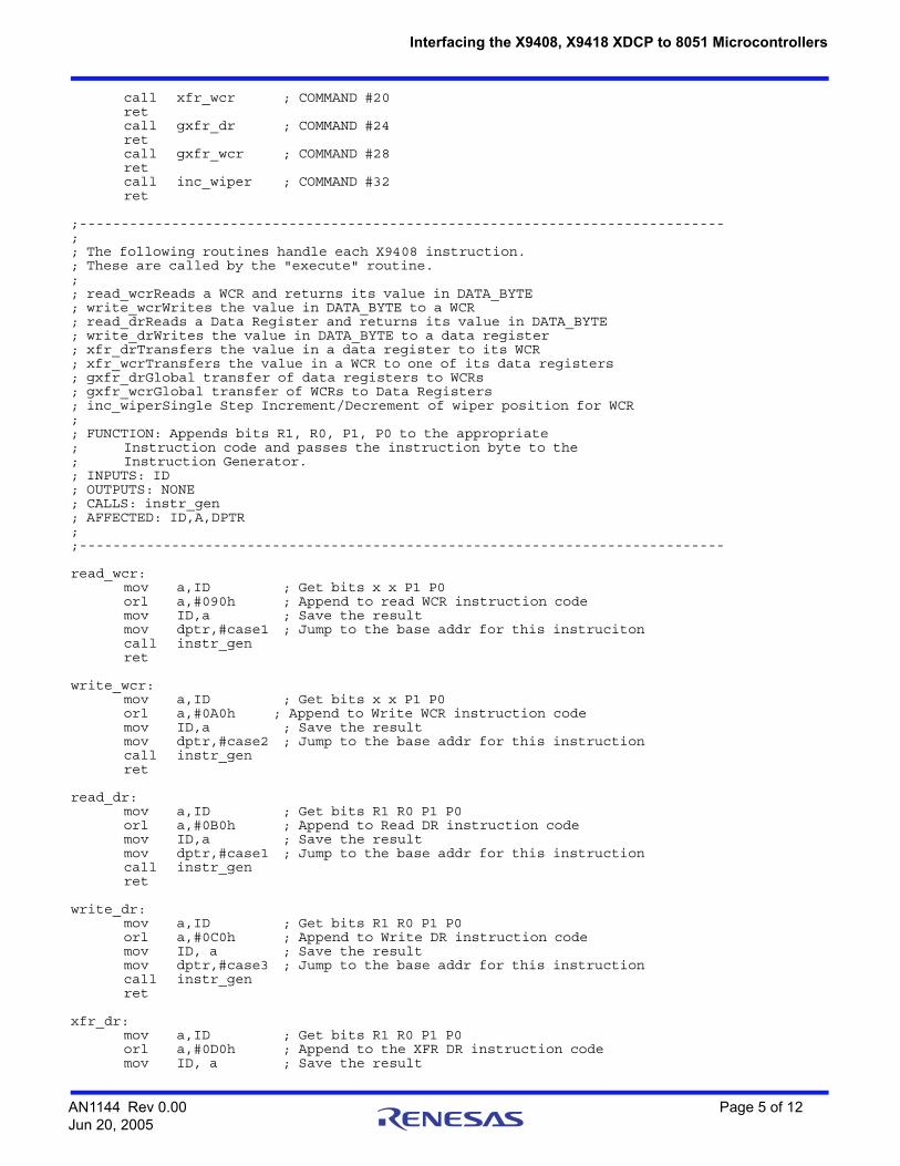
;-----------------------------------------------------------------------------; ; The following routines handle each X9408 instruction.; These are called by the "execute" routine.; ; read_wcrReads a WCR and returns its value in DATA_BYTE ; write_wcrWrites the value in DATA_BYTE to a WCR ; read_drReads a Data Register and returns its value in DATA_BYTE; write_drWrites the value in DATA_BYTE to a data register ; xfr_drTransfers the value in a data register to its WCR ; xfr_wcrTransfers the value in a WCR to one of its data registers; gxfr_drGlobal transfer of data registers to WCRs ; gxfr_wcrGlobal transfer of WCRs to Data Registers ; inc_wiperSingle Step Increment/Decrement of wiper position for WCR; ; FUNCTION: Appends bits R1, R0, P1, P0 to the appropriate; Instruction code and passes the instruction byte to the; Instruction Generator. ; INPUTS: ID ; OUTPUTS: NONE ; CALLS: instr_gen ; AFFECTED: ID,A,DPTR ; ;-----------------------------------------------------------------------------
read_wcr: mov a,ID ; Get bits x x P1 P0orl a,#090h ; Append to read WCR instruction codemov ID,a ; Save the resultmov dptr,#case1 ; Jump to the base addr for this instrucitoncall instr_genret
write_wcr: mov a,ID ; Get bits x x P1 P0orl a,#0A0h ; Append to Write WCR instruction codemov ID,a ; Save the resultmov dptr,#case2 ; Jump to the base addr for this instructioncall instr_genret
read_dr: mov a,ID ; Get bits R1 R0 P1 P0 orl a,#0B0h ; Append to Read DR instruction codemov ID,a ; Save the resultmov dptr,#case1 ; Jump to the base addr for this instructioncall instr_genret
write_dr: mov a,ID ; Get bits R1 R0 P1 P0orl a,#0C0h ; Append to Write DR instruction codemov ID, a ; Save the resultmov dptr,#case3 ; Jump to the base addr for this instructioncall instr_genret
xfr_dr: mov a,ID ; Get bits R1 R0 P1 P0orl a,#0D0h ; Append to the XFR DR instruction codemov ID, a ; Save the result
AN1144 Rev 0.00 Page 5 of 12Jun 20, 2005
Interfacing the X9408, X9418 XDCP to 8051 Microcontrollers
mov dptr,#case4 ; Jump to the addr for this instructioncall instr_gen ret
xfr_wcr: mov a,ID ; Get bits R1 R0 P1 P0orl a,#0E0h ; Append to the XFR WCR instruction codemov ID, a ; Save the resultmov dptr,#case5 ; Jump to the addr for this instructioncall instr_genret
gxfr_dr: mov a,ID ; Get bits R1 R0 x xorl a,#010h ; Append to the GXFR DR instruction codemov ID, a ; Save the resultmov dptr,#case4 ; Jump to the addr for this instructioncall instr_genret
gxfr_wcr: mov a,ID ; Get bits R1 R0 x xorl a,#080h ; Append to the GXFR WCR instruction codemov ID, a ; Save the resultmov dptr,#case5 ; Jump to the addr for this instructioncall instr_genret
inc_wiper: mov a,ID ; Get bits x x P1 P0orl a,#020h ; Append to the Incr Wiper instruction codemov ID,a ; Save the resultmov dptr,#case6 ; Jump to the addr for this instructioncall instr_genret
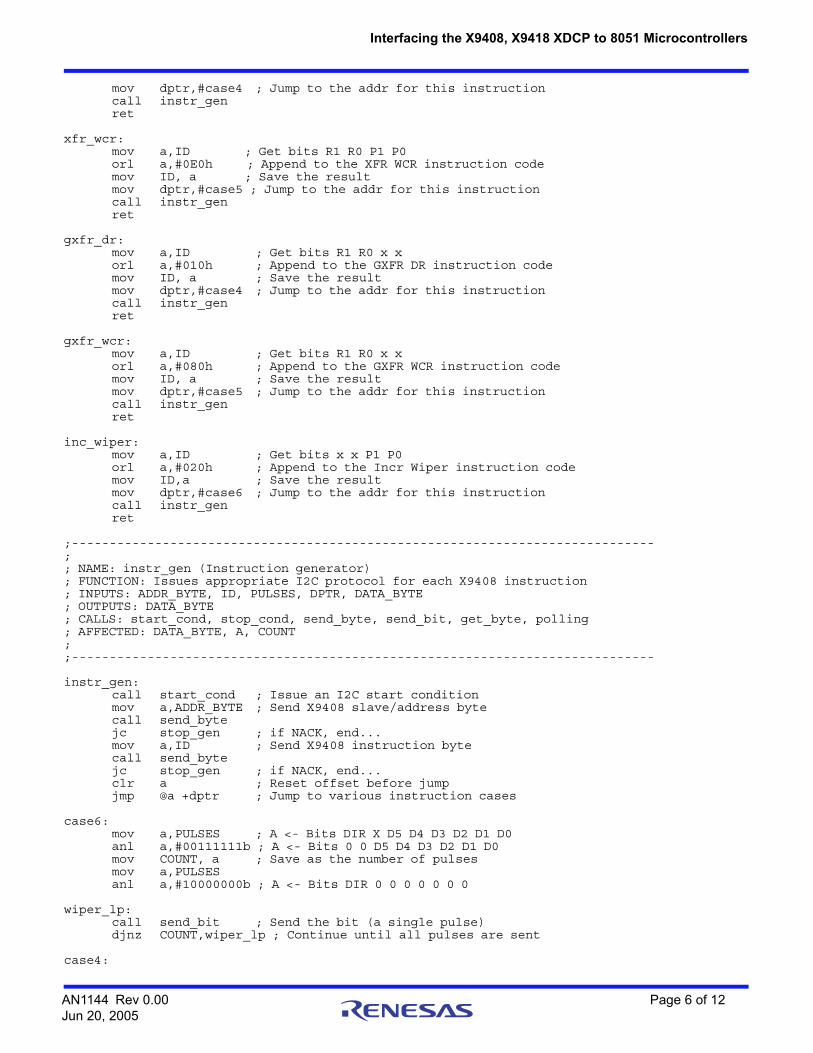
;-----------------------------------------------------------------------------; ; NAME: instr_gen (Instruction generator) ; FUNCTION: Issues appropriate I2C protocol for each X9408 instruction; INPUTS: ADDR_BYTE, ID, PULSES, DPTR, DATA_BYTE ; OUTPUTS: DATA_BYTE ; CALLS: start_cond, stop_cond, send_byte, send_bit, get_byte, polling; AFFECTED: DATA_BYTE, A, COUNT ; ;----------------------------------------------------------------------------- instr_gen:
call start_cond ; Issue an I2C start conditionmov a,ADDR_BYTE ; Send X9408 slave/address bytecall send_bytejc stop_gen ; if NACK, end...mov a,ID ; Send X9408 instruction bytecall send_bytejc stop_gen ; if NACK, end...clr a ; Reset offset before jumpjmp @a +dptr ; Jump to various instruction cases
case6: mov a,PULSES ; A <- Bits DIR X D5 D4 D3 D2 D1 D0anl a,#00111111b ; A <- Bits 0 0 D5 D4 D3 D2 D1 D0mov COUNT, a ; Save as the number of pulsesmov a,PULSESanl a,#10000000b ; A <- Bits DIR 0 0 0 0 0 0 0
wiper_lp: call send_bit ; Send the bit (a single pulse)djnz COUNT,wiper_lp ; Continue until all pulses are sent
case4:
AN1144 Rev 0.00 Page 6 of 12Jun 20, 2005
Interfacing the X9408, X9418 XDCP to 8051 Microcontrollers
jmp stop_gen ; If program gets here, then it is done
case2: mov a,DATA_BYTE ; Send X9408 data bytecall send_bytejmp stop_gen
case1: call get_byte ; Receive X9408 Data Bytejmp stop_gen
case3: mov a,DATA_BYTE ; Send X9408 Data Bytecall send_bytecall stop_cond ; Issue a stop conditioncall polling ; Begin Acknowledge Pollingjmp stop_gen
case5: call stop_cond ; Issue a stop conditioncall polling ; Begin Acknowledge Polling
stop_gen: call stop_cond ; I2C Transmission Over!ret
;-----------------------------------------------------------------------------; ; NAME: send_byte ; FUNCTION: Sends 8 bits (from MSB to LSB) to SDA and reads 1 bit from SDA ; INPUTS: A ; OUTPUTS: NONE ; CALLS: send_bit, get_bit ; AFFECTED: COUNT, TEMP, A ; ;-----------------------------------------------------------------------------
send_byte: mov COUNT,#8 ; Set loop for 8 repetitionsmov TEMP,a ; store as shifted byte (no shift)
bit_loop: mov a,TEMP ; Retrieve last saved shifted byteanl a,#10000000b ; Mask for MSB (Most Significant Bit)call send_bit ; Place this bit on SDA
next_bit: mov a,TEMP ; Retrieve last saved shifted byterl a ; Rotate all bits 1 position leftmov TEMP,a ; Store this updated shifted bytedjnz COUNT,bit_loopsetb SDA ; let SDA go high after 8th bitcall clock ; When all 8 bits done, read SDA line
; (ACKnowledge pulse)ret
;-----------------------------------------------------------------------------; ; NAME: send_bit ; FUNCTION: Places a bit on SDA and initiates a clock pulse on SCL; INPUTS: A ; OUTPUTS: NONE ; CALLS: clock ; AFFECTED: SDA ; ;-----------------------------------------------------------------------------
send_bit: clr SDA ; Pull SDA Lowjz sent_zero ; Should SDA really be LOW?
AN1144 Rev 0.00 Page 7 of 12Jun 20, 2005

Interfacing the X9408, X9418 XDCP to 8051 Microcontrollers
setb SDA ; If Not, pull SDA HIGH
sent_zero: call clock ; Initiate a clock pulseret
;-----------------------------------------------------------------------------; ; NAME: clock ; FUNCTION: Issues a LOW-HIGH-LOW clock pulse of sufficient duration; & reads SDA during the high phase, just in case its needed; INPUTS: NONE ; OUTPUTS: C ; CALLS: NONE ; AFFECTED: SCL, C ; ;-----------------------------------------------------------------------------clock:
nop ; Let SDA Set-upsetb SCL ; Pull SCL HIGH and holdnopnopnopmov c,SDA ; Move SDA bit into carry flagclr SCL ; Pull SCL LOWret
;-----------------------------------------------------------------------------; ; NAME: get_byte ; FUNCTION: Receives 8 bits from SDA (MSB to LSB) and sends 1 bit to SDA; INPUTS: NONE ; OUTPUTS: DATA_BYTE ; CALLS: clock, send_bit ; AFFECTED: COUNT, SDA, A, DATA_BYTE ; ;-----------------------------------------------------------------------------
get_byte: setb SDA ; Receiver shouldn't drive SDA lowmov COUNT,#8 ; Set Loop count to 8 repetitions
get_loop: call clock ; Clock in the current bitrlc a ; Reconstruct byte using left shiftsdjnz COUNT,get_loopmov DATA_BYTE,a ; Store retrieved Byte for userclr a ; A <- LOW (Sending a 0)call send_bit ; Send an acknowledgeret
;-----------------------------------------------------------------------------; ; NAME: start_cond (Start Condition) ; FUNCTION: Issues an I2C bus start condition ; INPUTS: NONE ; OUTPUTS: NONE ; CALLS: NONE ; AFFECTED: SDA, SCL ; ;----------------------------------------------------------------------------- start_cond:
setb SDA ; Pull SDA HIGH and allow set-upsetb SCL ; Pull SCL HIGH and holdnopnopnopnopclr SDA ;Pull SDA LOW (SCL=HIGH) and hold
AN1144 Rev 0.00 Page 8 of 12Jun 20, 2005

Interfacing the X9408, X9418 XDCP to 8051 Microcontrollers
nopnopnopnopclr SCL ;Complete clock pulse
ret
;-----------------------------------------------------------------------------; ; NAME: stop_cond (Stop condition) ; FUNCTION: Issues an I2C bus stop condition ; INPUTS: NONE ; OUTPUTS: NONE ; CALLS: NONE ; AFFECTED: SDA, SCL ; ;----------------------------------------------------------------------------- stop_cond:
clr SDA ; Pull SDA LOW and hold setb SCL ; Pull SCL HIGH and holdnopnopnopnopsetb SDA ; Pull SDA HIGH (SCL=HIGH)ret
;-----------------------------------------------------------------------------; ; NAME: ack_send (Send Acknowledge) ; FUNCTION: Sends an acknowledge bit to complete SDA line data reads; INPUTS: NONE ; OUTPUTS: NONE ; CALLS: send_bit ; AFFECTED: A ; ;-----------------------------------------------------------------------------
ack_send: clr a ; A <- LOW (Sending a 0)call SEND_BIT ; Send the bit!ret
;-----------------------------------------------------------------------------; ; NAME: polling (Acknowledge polling for XFR_WCR, WRITE_DR, GXFR_WCR); FUNCTION: Sends dummy commands to X9408 during an internal write cycle ; so that the end of the cycle is marked by an acknowledge; INPUTS: ADDR_BYTE ; OUTPUTS: NONE ; CALLS: start_cond, send_byte ; AFFECTED: C ; ;-----------------------------------------------------------------------------
polling: call START_COND ; Re-establish I2C protocolmov a,ADDR_BYTE ; Attempt to send a dummy command
again: call SEND_BYTEjc POLLING ; If C=1, then there was no ACK
ret
;-----------------------------------------------------------------------------; ; PUT MAIN PROGRAM HERE... ;
AN1144 Rev 0.00 Page 9 of 12Jun 20, 2005
Interfacing the X9408, X9418 XDCP to 8051 Microcontrollers
; Below are sample main programs calling the various command routines ; ;-----------------------------------------------------------------------------
main:
mov SP, #STACK_TOP; Initialize stack pointer
;----------------------------------------------------------------------------;; The following section is required for the Cygnal processor. This could; change for different versions of the 80C51.;; Disable the WDT. (IRQs not enabled at this point.); If interrupts were enabled, they would need to be explicitly disabled; so that the 2nd move to WDTCN occurs no more than four clock ; cycles after the first move to WDTCN.
clr EA ; Disable interupts
mov WDTCN, #0DEh; Cygnal processor specificmov WDTCN, #0ADh; Cygnal processor specific
; Enable the Port I/O Crossbar
mov XBR2, #40h ; Cygnal processor specific (enable weak pull ups)
mov PRT1CF, #00h ; Cygnal processor specific; Set no ports as push-pull (this processor; operates from 3.3V, but the X9408 operates from; 5V, so the 8051 outputs must be pulled up to 5V ; with external resistors.)
;-----------------------------------------------------------------------------;; The following are sample code segments for use in the main program...; The potentiometer was A0-A3 pins were set to address 0Ch.;;-----------------------------------------------------------------------------
write_2_wcr:mov ADDR_BYTE, #SLAVE_ADR12; Load Slave address bytemov ID, #WCR_2 ; Specify WCR for DCP#2 mov COMMAND, #WRITEWCR; Write to WCRmov DATA_BYTE, #43; Set wiper position to tap 43call execute
read_from_wcr:mov ADDR_BYTE, #SLAVE_ADR12; Load Slave address bytemov ID, #WCR_2 ; Specify WCR for DCP#2mov COMMAND, #READWCR; Read WCRcall execute ; WCR value is in DATA_BYTE
write_2_dr:mov ADDR_BYTE, #SLAVE_ADR12; Load Slave address bytemov ID, #DCP2_R1; Specify DR#1 for DCP#2 mov COMMAND, #WRITEDR; Write to DRmov DATA_BYTE, #21; Set data value to 21call execute
read_from_dr:mov ADDR_BYTE, #SLAVE_ADR12; Load Slave address bytemov ID, #DCP2_R1; Specify DR#1 for DCP#2mov COMMAND, #READDR; Read DRcall execute ; DR value is in DATA_BYTE
mov_dr_2_wcr:mov ADDR_BYTE, #SLAVE_ADR12; Load Slave address bytemov ID, #DCP2_R1; Specify DR#1 to WCR of DCP#2mov COMMAND, #XFRDR; Transfer DR to WCR
AN1144 Rev 0.00 Page 10 of 12Jun 20, 2005

Interfacing the X9408, X9418 XDCP to 8051 Microcontrollers
call execute
mov_wcr_2_dr:mov ADDR_BYTE, #SLAVE_ADR12; Load Slave address bytemov ID, #DCP2_R1; Specify WCR to DR#1 of DCP#2mov COMMAND, #XFRWCR; Transfer WCRto DRcall execute
global_dr_2_wcr:mov ADDR_BYTE, #SLAVE_ADR12; Load Slave address bytemov ID, #DR_1 ; Specify DR#1 to WCRmov COMMAND, #GXFRDR; Transfer DR to WCRcall execute
global_wcr_2_dr:mov ADDR_BYTE, #SLAVE_ADR12; Load Slave address bytemov ID, #DR_1 ; Specify WCR to DR#1 of DCP#2mov COMMAND, #GXFRWCR; Transfer WCRto DRcall execute
decr_wiper:mov ADDR_BYTE, #SLAVE_ADR12; Load Slave address bytemov ID, #WCR_2 ; Select DCP#2mov PULSES, #0Fh; Decrement DCP#2 for 16 pulsesmov COMMAND, #INCDECWIPER; INC wipercall execute
incr_wiper:mov ADDR_BYTE, #SLAVE_ADR12; Load Slave address bytemov ID, #WCR_2 ; Select DCP#2mov PULSES, #8Fh; Increment DCP#2 for 16 pulsesmov COMMAND, #INCDECWIPER; DEC wipercall execute
END
AN1144 Rev 0.00 Page 11 of 12Jun 20, 2005
http://www.renesas.comRefer to "http://www.renesas.com/" for the latest and detailed information.
Renesas Electronics America Inc.1001 Murphy Ranch Road, Milpitas, CA 95035, U.S.A.Tel: +1-408-432-8888, Fax: +1-408-434-5351Renesas Electronics Canada Limited9251 Yonge Street, Suite 8309 Richmond Hill, Ontario Canada L4C 9T3Tel: +1-905-237-2004Renesas Electronics Europe LimitedDukes Meadow, Millboard Road, Bourne End, Buckinghamshire, SL8 5FH, U.KTel: +44-1628-651-700, Fax: +44-1628-651-804Renesas Electronics Europe GmbHArcadiastrasse 10, 40472 Düsseldorf, Germany Tel: +49-211-6503-0, Fax: +49-211-6503-1327Renesas Electronics (China) Co., Ltd.Room 1709 Quantum Plaza, No.27 ZhichunLu, Haidian District, Beijing, 100191 P. R. ChinaTel: +86-10-8235-1155, Fax: +86-10-8235-7679Renesas Electronics (Shanghai) Co., Ltd.Unit 301, Tower A, Central Towers, 555 Langao Road, Putuo District, Shanghai, 200333 P. R. China Tel: +86-21-2226-0888, Fax: +86-21-2226-0999Renesas Electronics Hong Kong LimitedUnit 1601-1611, 16/F., Tower 2, Grand Century Place, 193 Prince Edward Road West, Mongkok, Kowloon, Hong KongTel: +852-2265-6688, Fax: +852 2886-9022Renesas Electronics Taiwan Co., Ltd.13F, No. 363, Fu Shing North Road, Taipei 10543, TaiwanTel: +886-2-8175-9600, Fax: +886 2-8175-9670Renesas Electronics Singapore Pte. Ltd.80 Bendemeer Road, Unit #06-02 Hyflux Innovation Centre, Singapore 339949Tel: +65-6213-0200, Fax: +65-6213-0300Renesas Electronics Malaysia Sdn.Bhd.Unit 1207, Block B, Menara Amcorp, Amcorp Trade Centre, No. 18, Jln Persiaran Barat, 46050 Petaling Jaya, Selangor Darul Ehsan, MalaysiaTel: +60-3-7955-9390, Fax: +60-3-7955-9510Renesas Electronics India Pvt. Ltd.No.777C, 100 Feet Road, HAL 2nd Stage, Indiranagar, Bangalore 560 038, IndiaTel: +91-80-67208700, Fax: +91-80-67208777Renesas Electronics Korea Co., Ltd.17F, KAMCO Yangjae Tower, 262, Gangnam-daero, Gangnam-gu, Seoul, 06265 KoreaTel: +82-2-558-3737, Fax: +82-2-558-5338
SALES OFFICES
© 2018 Renesas Electronics Corporation. All rights reserved.Colophon 7.0
(Rev.4.0-1 November 2017)
Notice
1. Descriptions of circuits, software and other related information in this document are provided only to illustrate the operation of semiconductor products and application examples. You are fully responsible for
the incorporation or any other use of the circuits, software, and information in the design of your product or system. Renesas Electronics disclaims any and all liability for any losses and damages incurred by
you or third parties arising from the use of these circuits, software, or information.
2. Renesas Electronics hereby expressly disclaims any warranties against and liability for infringement or any other claims involving patents, copyrights, or other intellectual property rights of third parties, by or
arising from the use of Renesas Electronics products or technical information described in this document, including but not limited to, the product data, drawings, charts, programs, algorithms, and application
examples.
3. No license, express, implied or otherwise, is granted hereby under any patents, copyrights or other intellectual property rights of Renesas Electronics or others.
4. You shall not alter, modify, copy, or reverse engineer any Renesas Electronics product, whether in whole or in part. Renesas Electronics disclaims any and all liability for any losses or damages incurred by
you or third parties arising from such alteration, modification, copying or reverse engineering.
5. Renesas Electronics products are classified according to the following two quality grades: “Standard” and “High Quality”. The intended applications for each Renesas Electronics product depends on the
product’s quality grade, as indicated below.
"Standard": Computers; office equipment; communications equipment; test and measurement equipment; audio and visual equipment; home electronic appliances; machine tools; personal electronic
equipment; industrial robots; etc.
"High Quality": Transportation equipment (automobiles, trains, ships, etc.); traffic control (traffic lights); large-scale communication equipment; key financial terminal systems; safety control equipment; etc.
Unless expressly designated as a high reliability product or a product for harsh environments in a Renesas Electronics data sheet or other Renesas Electronics document, Renesas Electronics products are
not intended or authorized for use in products or systems that may pose a direct threat to human life or bodily injury (artificial life support devices or systems; surgical implantations; etc.), or may cause
serious property damage (space system; undersea repeaters; nuclear power control systems; aircraft control systems; key plant systems; military equipment; etc.). Renesas Electronics disclaims any and all
liability for any damages or losses incurred by you or any third parties arising from the use of any Renesas Electronics product that is inconsistent with any Renesas Electronics data sheet, user’s manual or
other Renesas Electronics document.
6. When using Renesas Electronics products, refer to the latest product information (data sheets, user’s manuals, application notes, “General Notes for Handling and Using Semiconductor Devices” in the
reliability handbook, etc.), and ensure that usage conditions are within the ranges specified by Renesas Electronics with respect to maximum ratings, operating power supply voltage range, heat dissipation
characteristics, installation, etc. Renesas Electronics disclaims any and all liability for any malfunctions, failure or accident arising out of the use of Renesas Electronics products outside of such specified
ranges.
7. Although Renesas Electronics endeavors to improve the quality and reliability of Renesas Electronics products, semiconductor products have specific characteristics, such as the occurrence of failure at a
certain rate and malfunctions under certain use conditions. Unless designated as a high reliability product or a product for harsh environments in a Renesas Electronics data sheet or other Renesas
Electronics document, Renesas Electronics products are not subject to radiation resistance design. You are responsible for implementing safety measures to guard against the possibility of bodily injury, injury
or damage caused by fire, and/or danger to the public in the event of a failure or malfunction of Renesas Electronics products, such as safety design for hardware and software, including but not limited to
redundancy, fire control and malfunction prevention, appropriate treatment for aging degradation or any other appropriate measures. Because the evaluation of microcomputer software alone is very difficult
and impractical, you are responsible for evaluating the safety of the final products or systems manufactured by you.
8. Please contact a Renesas Electronics sales office for details as to environmental matters such as the environmental compatibility of each Renesas Electronics product. You are responsible for carefully and
sufficiently investigating applicable laws and regulations that regulate the inclusion or use of controlled substances, including without limitation, the EU RoHS Directive, and using Renesas Electronics
products in compliance with all these applicable laws and regulations. Renesas Electronics disclaims any and all liability for damages or losses occurring as a result of your noncompliance with applicable
laws and regulations.
9. Renesas Electronics products and technologies shall not be used for or incorporated into any products or systems whose manufacture, use, or sale is prohibited under any applicable domestic or foreign laws
or regulations. You shall comply with any applicable export control laws and regulations promulgated and administered by the governments of any countries asserting jurisdiction over the parties or
transactions.
10. It is the responsibility of the buyer or distributor of Renesas Electronics products, or any other party who distributes, disposes of, or otherwise sells or transfers the product to a third party, to notify such third
party in advance of the contents and conditions set forth in this document.
11. This document shall not be reprinted, reproduced or duplicated in any form, in whole or in part, without prior written consent of Renesas Electronics.
12. Please contact a Renesas Electronics sales office if you have any questions regarding the information contained in this document or Renesas Electronics products.
(Note 1) “Renesas Electronics” as used in this document means Renesas Electronics Corporation and also includes its directly or indirectly controlled subsidiaries.
(Note 2) “Renesas Electronics product(s)” means any product developed or manufactured by or for Renesas Electronics.