Embed Size (px)
Citation preview

AN11039General application note for OL2381Rev. 1 — 22 August 2011 Application note
Document information
Info Content
Keywords OL2381, BER
Abstract This document describes the OL2381 reference design board, explains the operation of the transmitter and receiver, and provides some application examples.

NXP Semiconductors AN11039General application note for OL2381
Revision history
Rev Date Description
1 20110822 first issue
AN11039 All information provided in this document is subject to legal disclaimers. © NXP B.V. 2011. All rights reserved.
Application note Rev. 1 — 22 August 2011 2 of 143
Contact informationFor more information, please visit: http://www.nxp.com
For sales office addresses, please send an email to: [email protected]

NXP Semiconductors AN11039General application note for OL2381
1. Introduction
This document describes typical applications for the OL2381. It shows a schematic and layout for an application board, describes procedures for setting up the transmitter with FSK and ASK modulation, explains in detail the analog and digital receiver blocks, and describes the procedure for measuring BER. Application examples are provided in Section 8 on page 120.
2. Reference design
2.1 Schematic
The application board must be carefully designed to achieve high receiver sensitivity and correct transmitter operation.
The power supply for the OL2381 requires careful consideration: The OL2381 accommodates four voltage regulators and a dedicated supply connection pin for each of the main functional blocks. All of these connections should be equipped with bypass capacitors to enable noise rejection. The voltage supply should have separate paths to minimize inductive and resistive coupling. All internal blocks are grounded via the exposed die pad on the bottom side of the package. A typical transceiver application using the OL2381 and external components is shown in Figure 1.
AN11039 All information provided in this document is subject to legal disclaimers. © NXP B.V. 2011. All rights reserved.
Application note Rev. 1 — 22 August 2011 3 of 143

xxxxxxxxxxxxxxxxxxxxx xxxxxxxxxxxxxxxxxxxxxxxxxx xxxxxxx x x x xxxxxxxxxxxxxxxxxxxxxxxxxxxxxx xxxxxxxxxxxxxxxxxxx xx xx xxxxx xxxxxxxxxxxxxxxxxxxxxxxxxxx xxxxxxxxxxxxxxxxxxx xxxxxx xxxxxxxxxxxxxxxxxxxxxxxxxxxxxxxxxxx xxxxxxxxxxxx x x xxxxxxxxxxxxxxxxxxxxx xxxxxxxxxxxxxxxxxxxxxxxxxxxxxx xxxxx xxxxxxxxxxxxxxxxxxxxxxxxxxxxxxxxxxxxxxxxxxxxxxxxxx xxxxxxxx xxxxxxxxxxxxxxxxxxxxxxxxx xxxxxxxxxxxxxxxxxxxx xxx
AN
11039
Ap
plicatio
n n
ote
NX
P S
emico
nd
ucto
rsA
N11039
Ge
nera
l ap
plic
ation
no
te fo
r OL
238
1
arked with a star * are UHF relevant e given to self-resonant frequency
001aan636
VDD100 nF 100 nF 100 nF 100 nF 100 nF 100 nF
22 nF
antenna
RFSWITCH
AD
DIT
ION
AL
FILT
ER
IF R
EQ
UIR
ED
AD
DIT
ION
AL
FILT
ER
IF R
EQ
UIR
ED
All information
provided in this do
cument is sub
ject to legal d
isclaimers.
© N
XP
B.V
. 2011. All rig
hts reserved.
Rev. 1
— 22 A
ug
ust 2011
4 of 143
The purpose of components used in this schematic is described in Table 1. All parts mmaterials and should be chosen according for this purpose. Special attention should b(SRF) and quality factor Q.
Fig 1. Reference design schematic
OL2381
P14/PINDXTAL1
XTAL2
RSTDIS
SEN
SDIO
SCLK
P11/INT
P12/CLOCKP13/SDO
TEN
TEST1
TEST2
TEST3
VREG_DIG
VREG_VCO
VREG_PLL
VREG_PA
RF_OUT
RF_IN
GN
D(p
in1)
VC
C_R
EG
VDD
GND
VC
C_D
IG
VC
C_X
O
VC
C_R
F
VC
C_I
F
VC
C_P
A
GN
D(p
in8)
GN
D(p
in9)
expo
sed
die
pad
GN
D(p
in16
)
GN
D(p
in32
)SPI/DATA
OPTIONAL
47 nF
22 nF
47 nF
1 μF
100 kΩ 100 kΩ 100 kΩ
P10/DATA

NXP Semiconductors AN11039General application note for OL2381
Table 1. Component description
Component Description
R1, R2, R3 Pull resistors are required to avoid floating voltage levels at the input ports SEN, SCLK and SDIO since a floating port contributes to increased current consumption. External resistors should be used if the connected SPI controller does not feature internal pull resistors. To disable the OL2381 properly, SEN should be pulled LOW. SCLK and SDIO could be either pulled HIGH or pulled LOW. The value of the external pull resistor should be less than or equal to 1 M.
X1, C2, C3 External reference crystal resonator components. The values of C2 and C3 should be chosen to support the crystal load capacitance. The values of both capacitors should be identical. If required, the value of C2 can be slightly less than the value of C3.
C1 The backup capacitor is specially required for battery supplied applications to avoid power failure during start-up at low temperature.
C4 to C15, L1 Noise decoupling capacitors for each OL2381 supply voltage connection pin. Each pin should be equipped with a 100 nF capacitor and a 100 pF capacitor* for high frequency rejection. The low value capacitor should be placed as close as possible to the corresponding supply voltage pin. L1 is optional and could be inserted in order to minimize feedback from the RF power amplifier to other OL2381 functional blocks; at the time of writing, the possibility of eliminating L1 is being investigated.
C16 to C19 A decoupling capacitor is required for each of the internal voltage regulator stages. The value of the capacitor should be chosen as shown in the schematic.
L2[1] The choke inductance L2 supplies power to the RF power amplifier. In addition L2 and C27 decouple UHF from the power supply.
L2 is part of the Class E matching network for the power amplifier and reduces the effective capacitance (Cbeff) at pin RF_OUT. The value of L2 should be chosen to set the matching according to output power requirements. 315 MHz applications with high output power may require the capacitance to be increased by connecting an additional capacitor directly to pin RF_OUT to GND.
L3[1], C30[1] Series resonant circuit of the Class E matching network. The quality of the circuit influences harmonic suppression.
L4[1], C31[1], C32[1] These elements form a LC low-pass Pi network. The network transforms the antenna impedance to a value required by the class E matching. The quality of the circuit influences harmonic suppression.
TX additional filter An additional filter may be required by the application to further increase harmonic suppression. A SAW filter should not be used in the TX path
L5[1], C40[1], C41[1] These elements form an LC high-pass T network. The network transforms the antenna impedance to the input impedance of RF_IN. A T network is used to minimize signal loss.
RX additional filter An additional filter may be required by the application to increase interfering signal rejection. A SAW filter can be used for this purpose.
RF_IN, RF_OUT If one of the functions is not used in an application the corresponding pin can remain open.
AN11039 All information provided in this document is subject to legal disclaimers. © NXP B.V. 2011. All rights reserved.
Application note Rev. 1 — 22 August 2011 5 of 143

NXP Semiconductors AN11039General application note for OL2381
[1] These are UHF relevant materials and should be chosen for this purpose. Special attention should be given to Self-Resonant Frequency (SRF) and quality factor Q.
2.2 Layout
An example of a PCB four layers layout is shown in Figure 2. Additional filters in the RX/TX paths, RF switch and antenna are not shown.
RF switch[1], P14 The switch combines the RX and TX signal path to a single antenna. OL2381 provides a control signal on P14 to set the state of the switch accordingly.
The switch can either comprise discrete components using pin diodes, or an RF switch IC.
If P14 is not used in the application it should remain open.
RSTDIS Pin RSTDIS should be connected to either GND or VCC. The initial condition of the polling timer is controlled by this pin.
SDO SDIO is the configurable bidirectional data input/output pin of the serial interface. By default, the bidirectional mode is configured, so SDIO is used for both input and output data transmission. If SEP_SDO in register PORTCON2 (address: 0x12) is set, SDIO is used as input only and SDO is configured for data output in SPI communication.
TEST1, TEST2 Pins to output analog test signals of the receiver unit in analog test mode. These pins can be used to debug the analog part of the receiver and so they are connected to test pads. Both pins can remain open.
TEN, TEST3 TEN must be grounded in the application. TEST3 must remain open.
P10, P11, P12 These ports enable communication between OL2381 and the microcontroller to be separate, allowing different lines for SPI communication and data communication in TX or RX mode.
After reset the ports are configured for digital output. It is not required to provide pull measurements for these ports.
These ports provide access to the receiver digital debug interface which requires the ports to be connected to test pads.
Table 1. Component description …continued
Component Description
AN11039 All information provided in this document is subject to legal disclaimers. © NXP B.V. 2011. All rights reserved.
Application note Rev. 1 — 22 August 2011 6 of 143

NXP Semiconductors AN11039General application note for OL2381
Guidelines for designing the layout are given in Table 2.
Blue: bottom layer; Purple: top layer.
Fig 2. Reference design layout
019aac090
AN11039 All information provided in this document is subject to legal disclaimers. © NXP B.V. 2011. All rights reserved.
Application note Rev. 1 — 22 August 2011 7 of 143

NXP Semiconductors AN11039General application note for OL2381
Table 2. Layout guidelines
Component Comment
Ground plane on bottom layer To achieve UHF power transportation with reduced effects due to human hand proximity, a ground plane below the UHF active module and the crystal resonator is recommended.
OL2381 functional blocks are connected to ground by the exposed die pad. It is important to have a good connection from the ground plane to the exposed die pad. Nine vias are used below OL2381 for this purpose.
Ground plane on top layer To reduce noise coupling via ground, several smaller ground fields are placed on the top layer. Special consideration should be given to the routing of the supply voltage bypass capacitors ground connection.
Ground planes on both layers should be connected by vias if possible.
Class E matching network The class E matching components should be placed close to OL2381 above the same ground plane. To setup the matching network properly, especially for high frequency bands, the connection between L2 and L3 as well as the distance to RF_OUT needs to be short to reduce capacitance to ground.
Long connections or vias between the components can cause additional inductance. This prevents effective filtering and increases unwanted inductive coupling. As a rule of thumb, each cm of PCB wire adds about 10 nH of inductance. This is true also for the ground connection back to the OL2381.
L2 and L3 should be placed perpendicular to each other in order to avoid magnetic coupling in-between the coils.
L3 and C30 should be placed close to each other without close ground planes on the top layer, to minimize parasitic capacitance to ground.
AN11039 All information provided in this document is subject to legal disclaimers. © NXP B.V. 2011. All rights reserved.
Application note Rev. 1 — 22 August 2011 8 of 143

NXP Semiconductors AN11039General application note for OL2381
EMC measurements are given in Section 9 on page 126 with the reference design presented above.
2.3 RF switch
The easiest implementation of the RF switch (transmit/receive) is the single control IC, such as the California Eastern Lab UPD5713. The switch should be controlled by the OL2381 pin P14/IND. When pin P14/IND is LOW, receive mode is activated, and when it is HIGH, transmit mode is activated. OL2381 register PORTCON2 operation bits [2:1] (P14C) should be set to 11 for correct operation; see Figure 43 on page 39.
Dual control ICs can be used. In this case, the switch should be controlled by OL2381 pins P13 and P14.
IC switches available on the market are specified from 45 C to +85 C. If the application requires an extended temperature range, the RF switch should comprise discrete components using PIN diodes.
Figure 3 shows the typical quarter wavelength switch and associated grouped elements required for 868 MHz operation. The quarter wavelength circuit (formed by C4, C5, and L2) mainly serves to isolate the transmit path from the receiver input. The PIN diode switch also uses the drive capability of OL2381 pin P14/PIND. When both diodes are forward biased (P14/PIND is HIGH), the transmitter is connected to the antenna and the receiver is protected by the low resistance of D2 terminating the quarter-wavelength line which makes an open-circuit at point A. This allows the signal from TX50OHMS to flow through D1 to the antenna. When both diodes are reverse biased (P14/PIND is LOW) the transmitted port is isolated by the high resistance of D1 and the antenna is connected to
Passive components Most of the components are size 0402 to keep the required PCB space small. In particular, the bypass capacitors at the supply voltage input of OL2381 should be small to place the components close to the IC.
The coils in the TX path (L2, L3, and L4) are wound type size 0603. These coils show a good quality factor in order to reduce power loss for the transmitted signal.
In particular, for the low frequency bands L2 should be a high Q coil with a high SFR value. High output power at 315 MHz requires L2 to have a high value in order to get enough capacitance at RF_OUT. Some applications may require an extra capacitor to be connected between RF_OUT and ground.
The capacitors in the TX and RX paths including the low value bypass capacitors at the voltage ports should be NP0 type. The components in the RF paths and capacitors C1/C2 should have tight tolerance.
C3 The backup capacitor has a value of 1 F. The component should show low leakage current over the whole temperature range of the application. The device shown in the layout is an X7R type, size 0805.
Crystal resonator The crystal and corresponding capacitors should be placed close to XTAL1 and XTAL2 to minimize parasitic PCB capacitance and so decrease unwanted detuning due to human hand proximity in hand-held applications.
Table 2. Layout guidelines
Component Comment
AN11039 All information provided in this document is subject to legal disclaimers. © NXP B.V. 2011. All rights reserved.
Application note Rev. 1 — 22 August 2011 9 of 143

NXP Semiconductors AN11039General application note for OL2381
RX50OHMS. The high impedance of D2 is transformed to a short-circuit at point A through the quarter wavelength line. Figure 4 and Figure 5 show simulation setup and results for the transmit path. TX50OHMS and RX50OHMS are already matched OL2381 receiver and transmitter ports to 50 W. DC blocking is required by either PIN diode or IC switch, so if series capacitors are used in the receiver, transmitter, and antenna matching networks, then capacitors C1, C6, and C3 can be omitted.
The quarter wavelength transformer has a relatively narrow band response. Instead of C4, C5, and L2, the quarter wavelength line (microstrip line on the PCB) can be used. The quarter wavelength line constrains the bandwidth from 5 % to 10 %. Therefore, for different frequency bands, a different PCB is required.
Advantages of the IC switch compared to the PIN diode switch are: broadband, low insertion loss, good isolation, and small size. Advantages of the PIN diode switch compared to the IC switch are: cost, good linearity, high power applications, and temperature range.
Resistor R1 can be calculated from P14/PIND voltage in the application and diode parameters (forward voltage and current): R1 = (VCC 2 VF) / ID.
Fig 3. RF pin diode switch schematic
019aac091
R1330 Ω
C1 D1
NXP BAP63-0256 pF
C6
56 pF
L2
10 nH
C2
68 pF L168 nH
C356 pF
C43.3 pF
C53.3 pF
D2NXP BAP63-02
TX50OHMS RX50OHMS
P14
GND
GND
antenna
point A
AN11039 All information provided in this document is subject to legal disclaimers. © NXP B.V. 2011. All rights reserved.
Application note Rev. 1 — 22 August 2011 10 of 143

NXP Semiconductors AN11039General application note for OL2381
Results are similar for the receive path and are available on request.
3. Interface description
There are two possibilities to send or receive data with the OL2381: by using the SPI pins or by using the general port pins. Registers PORTCON0, PORTCON1 and PORTCON2 (address: 0x10 to 0x12) need to be properly configured. PORTCON0 configures P10/DATA and P11/INT, PORTCON1 configures P12/CLOCK and P13/SDO and
Fig 4. Transmit path schematic
019aac092
Term1Num = 1Z = 50 Ω
Term2Num = 2Z = 50 Ω
Term3Num = 3Z = 50 Ω
L3LQW18pn = LQW18AN68NG00
C9pn = GRM1555C1H560JZ01
C14GRM15
pn = GRM1555C1H3R3CZ01
I_DCSRC2Idc = 10 mA
C15 L7
0.15 nHTX RX
P14RX
ANTENNA
S-PARAMETERS
SP1START = 800 MHzSTOP = 936 MHzSTEP = 1 MHz
GRM15pn = GRM1555C1H560JZ01
C10
GRM15pn = GRM1555C1H101JZ01
L8
0.1 nH
L12
LQW15pn = LQW15AN10HN00
L6
0.45 nH
PIN_diode
NXP BAP63-02
PIN_diodeNXP BAP63-02
C11
90 fF
C18
pn = GRM1555C1H560JZ01L90.15 nH
L110.45 nH C12
90 fF
L100.1 nH
S-PARAMETERS
SP2START = 100 MHzSTOP = 1600 MHzSTEP = 1 MHz
Fig 5. Transmit path results
019aac094
AN11039 All information provided in this document is subject to legal disclaimers. © NXP B.V. 2011. All rights reserved.
Application note Rev. 1 — 22 August 2011 11 of 143
NXP Semiconductors AN11039General application note for OL2381
PORTCON2 configures P14/PIND and the TX/RX lines. Reset values are: PORTCON0 0x28, PORTCON1 0x0E, and PORTCON2 0x00. Further details are explained in the OL2381 data sheet.
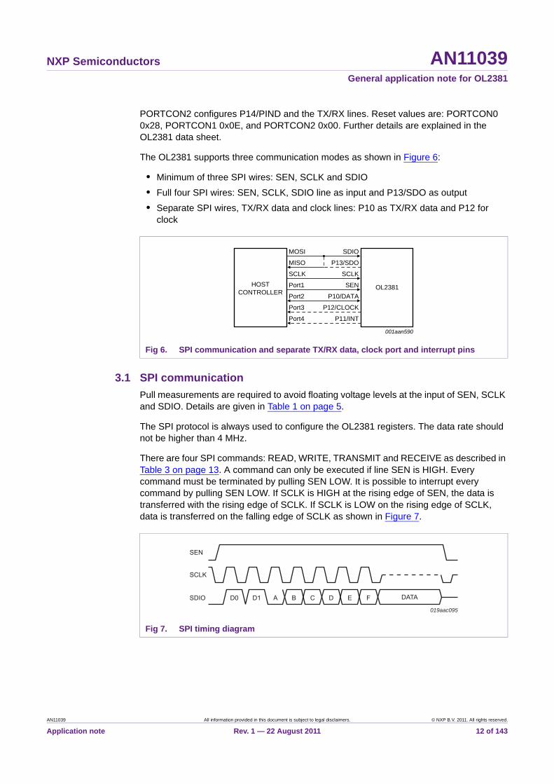
The OL2381 supports three communication modes as shown in Figure 6:
• Minimum of three SPI wires: SEN, SCLK and SDIO
• Full four SPI wires: SEN, SCLK, SDIO line as input and P13/SDO as output
• Separate SPI wires, TX/RX data and clock lines: P10 as TX/RX data and P12 for clock
3.1 SPI communication
Pull measurements are required to avoid floating voltage levels at the input of SEN, SCLK and SDIO. Details are given in Table 1 on page 5.
The SPI protocol is always used to configure the OL2381 registers. The data rate should not be higher than 4 MHz.
There are four SPI commands: READ, WRITE, TRANSMIT and RECEIVE as described in Table 3 on page 13. A command can only be executed if line SEN is HIGH. Every command must be terminated by pulling SEN LOW. It is possible to interrupt every command by pulling SEN LOW. If SCLK is HIGH at the rising edge of SEN, the data is transferred with the rising edge of SCLK. If SCLK is LOW on the rising edge of SCLK, data is transferred on the falling edge of SCLK as shown in Figure 7.
Fig 6. SPI communication and separate TX/RX data, clock port and interrupt pins
001aan590
MOSI
HOSTCONTROLLER
OL2381
MISO
SCLK
Port1
Port2
Port3
Port4
SDIO
P13/SDO
SCLK
SEN
P10/DATA
P12/CLOCK
P11/INT
Fig 7. SPI timing diagram
019aac095
SDIO
SCLK
SEN
D0 D1 A B C D E F DATA
AN11039 All information provided in this document is subject to legal disclaimers. © NXP B.V. 2011. All rights reserved.
Application note Rev. 1 — 22 August 2011 12 of 143

NXP Semiconductors AN11039General application note for OL2381
Figure 8 shows an oscilloscope view of the SPI communication. The yellow trace represents the SEN line, the pink trace the SDIO line and the blue trace the SCLK line.
After line SEN goes down and up, data is transferred to OL2381 according to Figure 7. This can be seen in Figure 8. The first SPI command is write command (00b) to the address of 0x11 (010010b) which corresponds to register PORTCON1. The value 0x78 (0111 1000b) is then written to this register.
The second SPI command is read command (01b) from address 0x11 (010010b) which corresponds to register PORTCON1. The value 0x78 (0111 1000b) is then read from this register.
Figure 9 shows a read command with four lines: SEN, SCLK, SDI and SDO (SPI interface). In this case, bit SEP_SDO in register PORTCON2 must be set to logic 1.
Table 3. SPI commands
D0 D1 Command A to F
0 0 write SFR start address A5 to A0
0 1 read SFR start address A5 to A0
1 0 receive receive options
1 1 transmit transmit options
(1) Yellow trace: SEN.
(2) Pink trace: SDIO.
(3) Blue trace: SCLK.
Fig 8. Oscilloscope SPI signals
019aac096
AN11039 All information provided in this document is subject to legal disclaimers. © NXP B.V. 2011. All rights reserved.
Application note Rev. 1 — 22 August 2011 13 of 143

NXP Semiconductors AN11039General application note for OL2381
When a SPI data communication is used as shown in Figure 10, the SPI pins are used to configure the OL2381 registers and to exchange data.
Bits SEP_TX_LINES and SEP_RX_OUT in register PORTCON2 should be set to logic 00 for a SPI data communication. This is shown in Figure 11.
SEP_SDO = 1.
Fig 9. Four SPI lines of a read command
Fig 10. OL2381 configuration for SPI communication
Fig 11. PORTCON2 register set for SPI data communication
SEN
SCLK
SDIO
SDO
019aac097
001aan590
MOSI
HOSTCONTROLLER
OL2381
MISO
SCLK
Port1
Port2
Port3
Port4
SDIO
P13/SDO
SCLK
SEN
P10/DATA
P12/CLOCK
P11/INT
019aac098
AN11039 All information provided in this document is subject to legal disclaimers. © NXP B.V. 2011. All rights reserved.
Application note Rev. 1 — 22 August 2011 14 of 143

NXP Semiconductors AN11039General application note for OL2381
Figure 12 and Figure 13 show transmit and receive data timing diagrams when SPI data communication is used.
Fig 12. Transmit data timing diagram (SEP_TX_LINES = 0)
Fig 13. Receive data timing diagram (SEP_RX_LINES = 0)
019aac099
registers transmit data
SDIO
SCLK
SEN
019aac100
SDIO Tx
SDIO Rx
SEN Rx
SCLK Rx
Registers via SPI Rx data received via SPI
AN11039 All information provided in this document is subject to legal disclaimers. © NXP B.V. 2011. All rights reserved.
Application note Rev. 1 — 22 August 2011 15 of 143

NXP Semiconductors AN11039General application note for OL2381
3.2 Port communication
Figure 14 shows the block diagram of the port in-use communication. The SPI pins are used to configure the OL2381 registers. Ports P10, P11, and P12 are used to send or receive data, clock and interrupt.
Pin P10/DATA is used for TX/RX data input/output, P12/CLOCK delivers the associated clock signal and P11/INT can be configured for data or interrupt output between the OL2381 and host controller.
These three output pins deliver the result of the receiver when it is configured for normal mode. DATA is the data output, CLOCK delivers the associated clock signal and INT is usually used as an interrupt request.
By setting the register field RXD_DBG_SEL in register TEST0 (address: 0x35) to a non-zero value, the receiver is configured for digital debug mode. In this mode, normal function of ports (P10, P11, and P12) is overwritten with the fast 3-wire synchronous serial interface function. In this mode P12 outputs 16 MHz serial clock, P10 outputs the serial data, and P11 outputs a synchronization pulse for each serial 16-bit data word.
The protocol used in this mode is shown in Figure 15. In this case, the OL2381’s current consumption will increase by 5 mA.
Bits SEP_TX_LINES and SEP_RX_OUT in register PORTCON2 (see Figure 11 on page 14) should be set to logic 11 for normal port data communication.
Table 4 gives the port configuration summary.
Fig 14. OL2381 Configuration for port communication
001aan590
MOSI
HOSTCONTROLLER
OL2381
MISO
SCLK
Port1
Port2
Port3
Port4
SDIO
P13/SDO
SCLK
SEN
P10/DATA
P12/CLOCK
P11/INT
Fig 15. Serial test vector interface format
019aac101
bit 2
CLOCK
DATA
FRAME
bit 1 bit 0 bit 15 bit 14 bit 2 bit 1 bit 0 bit 15 bit 14
AN11039 All information provided in this document is subject to legal disclaimers. © NXP B.V. 2011. All rights reserved.
Application note Rev. 1 — 22 August 2011 16 of 143

NXP Semiconductors AN11039General application note for OL2381
Figure 16 and Figure 17 show transmit and receive data timing diagrams when port communication is used.
Table 4. Port configuration
Description PORTCON0 PORTCON1 PORTCON2
Value: 0x28 0x04 0x66
Ports: P10/DATA P11/INT P12/CLOCK P13/SDO P14 SEP_RX_OUT, SEP_TX_LINES
Configuration: P10 is in 3-state mode
P11 = 0010b + P11 INV; P11 behaves as interrupt request
P12 provides the RX/TX clock output
P13 is in 3-state mode
P14 controls the RF switch
P10 is always used as RX/TX data and P12 as RX/TX clock output
Fig 16. Transmit data timing diagram (SEP_TX_LINES = 1)
019aac102
Registers via SPI Transmit data sent via port
SCLK
SDIO
P12/CLOCK
P10/DATA
AN11039 All information provided in this document is subject to legal disclaimers. © NXP B.V. 2011. All rights reserved.
Application note Rev. 1 — 22 August 2011 17 of 143

NXP Semiconductors AN11039General application note for OL2381
4. Phase-locked loop
The complete on-chip Phase Locked Loop (PLL) provides an RF carrier both in the Transmit (TX) and Receive (RX) mode. The PLL is a 4th-order fractional-N PLL. It is designed for a current output phase detector. It comprises a 2nd-order integrating filter, followed by an additional pole to reduce the phase reference spur modulation of the VCO. The PLL main divider consists of one fixed (divided by 2) and five switched dividers (5 control bits for 32 different divider settings) with a range of 64 to126. More details are given in the OL2381 data sheet.
All PLL blocks except VCO_BAND and the charge pump current (ICP_PLL settings) are automatically configured and operated by selecting the corresponding device modes. Two bits (DEV_MODE[3:2]) in register PWRMODE (address: 0x13), control the active modes of the device.
Fig 17. Receive data timing diagram (SEP_RX_LINES = 1)
019aac103
SDIO Tx
SDIO Rx
SCLK Rx
P10/DATA RX
Registers via SPI Rx data received via port
Fig 18. PWRMODE register when PLL is activated
019aac104
AN11039 All information provided in this document is subject to legal disclaimers. © NXP B.V. 2011. All rights reserved.
Application note Rev. 1 — 22 August 2011 18 of 143

NXP Semiconductors AN11039General application note for OL2381
Three important static enable signals are decoded from the DEV_MODE, namely PLLEN, TXEN and RXEN. PLLEN is set whenever the DEV_MODE is not logic 00. These three signals are internal and not accessible to customers.
4.1 PLL operation
The charge pump delivers charge to the loop filter. The polarity and amount of charge are proportional to the phase error reported by the phase detector (PFD). The five PLL_ICP control bits in register EXPERT0 (address: 0x31) shown in Figure 19, are reserved for manual programming of PLL charge pump current. The value from 15 A to 465 A can be selected with the formula: Icp = PLL_ICP 15 A.
The recommended value is ICP2.
The lock detection circuit monitors the phase and frequency difference of PLL in order to detect the shortest PLL power-on time. The lock detection circuit can be manually controlled by bit LOCK_DET_ON in register LOCON (address: 0x0D). After the time defined by bits LOCK_DET_TIME in register EXPERT1 (Figure 22 on page 23), status bit LO_RDY is set in register DEVSTATUS (address: 0x19).
4.2 Operating frequency
The PLL operating frequency is set by registers FC0x (address: 0x00 to 0x01 to 0x02), FC1x (address: 0x03 to 0x05), FC2x (address: 0x06 to 0x08), and FC3x (address: 0x09 to 0x0B). Each of them (0, 1, 2, or 3) has a width of 20 bits and can be selected directly with bits A and B in transmit or receive command.
The selection and description of the frequency control registers are given in Table 6.
Table 5. DEV_MODE[1:0] device mode control functions
D3 D2 Function
0 0 crystal oscillator or external clock buffer is enabled and after crystal oscillator stabilization (if selected) the device is supplied with the reference clock
0 1 PLL controlled local oscillator (LO) enabled. LO power-up procedure includes VCO sub-band calibration (unconditionally) and PLL lock-in detection
1 0 prepare and enable RX operation. LO enabled and after PLL acquires lock, RX is switched on and enabled
1 1 prepare and enable TX operation. LO enabled and after PLL acquires lock, TX path and PA regulator are switched on and enabled.
Fig 19. Register EXPERT0
019aac105
AN11039 All information provided in this document is subject to legal disclaimers. © NXP B.V. 2011. All rights reserved.
Application note Rev. 1 — 22 August 2011 19 of 143

NXP Semiconductors AN11039General application note for OL2381
The frequency control registers (FCxL, FCxM and FCxH) contain the integer and fractional part of the operating frequency described in Table 7.
The 20 binary bits in the PLL frequency registers can be calculated using the formula Equation 1 when bit DOUBLE_SD_RESULT = logic 0.
(1)
Where: fRF is the frequency to be computed (434 MHz), Fref is the crystal reference frequency, which for this application is 16 MHz.
It is possible to determine the values of the three registers FCxH, FCxM and FCxL when bit DOUBLE_SD_RESULT = logic 1 by using the inverse function of the frequency shown in Equation 2, Equation 3 and Equation 4.
(2)
(3)
(4)
Where:
fRF is the frequency to be computed, here 434 MHz.
fref is the crystal reference frequency, which for this application is 16 MHz.
FCx[19:15] corresponds to the integer bits.
FCx[14:0] corresponds to the fractional part bits.
Table 8 presents the configuration registers for some OL2381 operating frequencies.
Table 6. Frequency selection register bit settings
A (TX or RX) B (TX or RX) Selected frequency registers
0 0 FC0L, FC0M, FC0H
0 1 FC1L, FC1M, FC1H
1 0 FC2L, FC2M, FC2H
1 1 FC3L, FC3M, FC3H
Table 7. Frequency setting registers
Register Bit
7 (MSB) 6 5 4 3 2 1 0 (LSB)
FCxL Lower 4 bits of fractional part of operating frequency FCx not used
FCxM Middle 8 bits of fractional part of operating frequency FCx
FCxH 5 integer bits of operating frequency higher 3 bits of fractional part
FCxfRF
fref------- 1 RF_LO_DIV+ 32– 32768=
fRF fref 32 FCx 19:15 2 FCx 14:0 1+32768
---------------------------------------------+ + 1
1 RF_LO_DIV+-----------------------------------------=
FCx 19:15 fRF
fref------- 1 RF_LO_DIV+ 32.5–=
FCx 14:0 fRF
fref------- 1 RF_LO_DIV+ 32 FCx 19:15 ––
16384=
AN11039 All information provided in this document is subject to legal disclaimers. © NXP B.V. 2011. All rights reserved.
Application note Rev. 1 — 22 August 2011 20 of 143

NXP Semiconductors AN11039General application note for OL2381
Some frequency settings should not be used. More details are given in Section 4.3.3 on page 24.
4.2.1 VCO auto calibration and sub-band selection
The VCO calibration is performed when the VCO is turned on and every time when:
• the frequency changes with a transmit or receive command,
• the MSByte of the currently selected frequency setting changes,
• the VCO band changes with bit VCO_BAND,
• the sigma-delta mode changes with DOUBLE_SD_RESULT,
• switching between TX and RX.
The automatic VCO calibration can be suppressed in the some cases (more details are given in the OL2381 data sheet) by setting bit SKIP_VCO_CAL in register LOCON. The resulting sub-band settings from the VCO calibration can be read out via bit VCO_SUBBAND in register VCOCON. This value can be overwritten at any time by the microcontroller. If the value is written during an ongoing calibration, the result will become undefined. The FORCE_VCO_CAL bit in register VCOCON can be used to start a VCO calibration unconditionally on microcontroller request.
The VCO auto-calibration routine automatically trims the VCO to the correct sub-band whenever a different frequency setting is used in TX or RX operation and VCO calibration is carried out automatically. The sub-band selection can be manually modified by control bits VCO_SUBBAND in register VCOCON as shown in Figure 20.
Bit RF_LO_DIV in register LOCON (address: 0x0D) defines the division factor for VCO frequency. If RF_LO_DIV is logic 0, the VCO frequency is divided by 2 to achieve an operating frequency above 500 MHz. If RF_LO_DIV is logic 1, the VCO frequency is divided by 4 to achieve the operating frequency below 500 MHz.
Table 8. Frequency selection registers bits setting for different carrier frequencies
Frequency (MHz) Frequency selection registers RF_LO_DIV
FCxH FCxM FCxL
315 0x3B 0x00 0x00 1
434 0xB2 0x00 0x00 1
868 0xB2 0x00 0x00 0
915 0xC9 0x80 0x00 0
Fig 20. Register VCOCON
019aac106
AN11039 All information provided in this document is subject to legal disclaimers. © NXP B.V. 2011. All rights reserved.
Application note Rev. 1 — 22 August 2011 21 of 143

NXP Semiconductors AN11039General application note for OL2381
Bit VCO_BAND in register LOCON must be set to logic 1 for frequency bands below 400 MHz while it is zero for all other bands. In this case the VCO frequency is divided by 2. The VCO is running at twice (868 MHz and 915 MHz) and four times (315 MHz and 434 MHz) the selected frequency band as described in Table 9.
4.3 PLL measurement results
4.3.1 Phase noise measurements
Figure 21 shows the measured phase noise results for 434 MHz. The results for other frequency bands (315 MHz, 868 MHz and 915 MHz) are similar and available upon request.
The PLL loop bandwidth set by PLL_ICP2 is the best trade-off between noise behaviors and locking time. It is recommended that the PLL loop bandwidth should be set to 150 kHz.
At low frequency bands (315 MHz or 434 MHz), an internal divider is used in the PLL to provide the required frequency. When this divider is on, the phase noise is about 6 dB lower than for the high frequency bands (868 MHz or 915 MHz).
Table 9. VCO and carrier output frequencies
Device Frequency (MHz) RF VCO (MHz)
Min Typ Max
OL2381 VCO bands
300 315 320 300 MHz x 4 to 320 MHz x 4 = 1200 MHz to 1280 MHz
415 434 450 415 MHz x 4 to 928 MHz x 2 = 1660 MHz to 1856 MHz
865 868 870
902 915 928
AN11039 All information provided in this document is subject to legal disclaimers. © NXP B.V. 2011. All rights reserved.
Application note Rev. 1 — 22 August 2011 22 of 143

NXP Semiconductors AN11039General application note for OL2381
4.3.2 PLL locking time
The lock detection circuit monitors the phase and frequency difference of the PLL and reference clock. The status bit LO_RDY is set in register DEVSTATUS (address: 0x19) after an additional delay specified by bits LOCK_DET_TIME in register EXPERT1 (address: 0x32).
The setup for measuring the PLL locking time is:
• Set register PORTCON0 to 0101xxxx to make the LO_RDY flag bit appear at output pin P11/INT
• The PLL is set whenever bits DEV_MODE[3:2] in register PWRMODE are not zero [00]. Switching bits DEV_MODE from [00] to any other state can be used as a reference start time for PLL locking time measurement
• Set the oscilloscope trigger to LO_RDY flag (P11/INT).
(1) ICP1.
(2) ICP2.
(3) ICP3.
(4) ICP4.
(5) ICP5.
Fig 21. Phase noise at 434 MHz and different ICP settings
019aac107
f (Hz)103 107106105104
-120
-100
-80
φn(dB)
-140
(1)(2)(3)(4)(5)
Fig 22. Register EXPERT1
019aac108
AN11039 All information provided in this document is subject to legal disclaimers. © NXP B.V. 2011. All rights reserved.
Application note Rev. 1 — 22 August 2011 23 of 143

NXP Semiconductors AN11039General application note for OL2381
• After switching the DEV_MODE bits from [00] to any other state, measure the time from last SPI clock (SCLK) to the time when LO_RDY flag goes HIGH (PLL locked). It should be close to 120 s.
Figure 23 shows the results for PLL locking time. The measurement is performed with the charge pump current ICP2 setting.
In Figure 23, the yellow trace is the LO_RDY flag signal at pin P11/INT, the red trace is the write command data on SPI line SDIO, and the blue trace is the SPI clock measured on pin SCLK. PLL locking time is close to 120 s.
4.3.3 Frequency range
4.3.3.1 Inappropriate FC settings
For specific settings of the frequency control value FC, the OL2381 fractional-N PLL creates a frequency modulated output instead of a clean carrier signal. The disturbing signal could be observed in the output signal frequency spectrum appearing as spurious emissions close to the carrier frequency. The modulation frequency and the FM modulation index of the disturbing signal depend directly on the FC settings.
Fig 23. PLL locking time measurement on oscilloscope
019aac109
AN11039 All information provided in this document is subject to legal disclaimers. © NXP B.V. 2011. All rights reserved.
Application note Rev. 1 — 22 August 2011 24 of 143

NXP Semiconductors AN11039General application note for OL2381
If the 14 LSBits of FC are interpreted as a signed integer, the modulation frequency of the disturber increases with the absolute value of this number. Due to the filter function of the PLL loop filter, the modulation index depends on the modulation frequency of the disturber. With the recommended setting of ICP = 2 the maximum modulation index is about 1 / 5, in other words the maximum power in the spurious emission is 20 dBc.
In order to minimize the influence of the disturbing signal to the application, especially if OL2381 is in receive mode, and to avoid interference with adjacent channels in transmit mode, some values of FC should be avoided.
RF_LO_DIV = 1 (256 MHz to 512 MHz)
a range of 1024 should be avoided around FC = N 216 (0 N 16)
a range of 512 should be avoided around FC = N 215 (0 N 32)
a range of 256 should be avoided around FC = N 214 (0 N 64)
Fig 24. FC = B0000h, RF_LO_DIV = 0
Fig 25. FC = B0050h, RF_LO_DIV = 0
019aac110
Ref 10 dBm Att 20 dB*
A
Center 864 MHz Span 5 kHz500 Hz/
*
3DB
RBW 30 HzVBW 100 HzSWT 5.6 s
*1 PKVIEW
-90
-80
-70
-60
-50
-40
-30
-20
-10
0
101
Marker 1 [T1 ]7.72 dBm
864.000015000 MHz
2
Delta 2 [T1 ]-24.37 dB
-245.000000000 Hz
019aac111
Ref 10 dBm Att 20 dB*
A
Center 864.04 MHz Span 400 kHz40 kHz/
*RBW 3 kHzVBW 10 kHzSWT 45 ms
3DB
*1 PKVIEW
-90
-80
-70
-60
-50
-40
-30
-20
-10
0
101
Marker 1 [T1 ]7.75 dBm
864.039600000 MHz
2
Delta 2 [T1 ]-22.26 dB
-39.600000000 kHz
AN11039 All information provided in this document is subject to legal disclaimers. © NXP B.V. 2011. All rights reserved.
Application note Rev. 1 — 22 August 2011 25 of 143

NXP Semiconductors AN11039General application note for OL2381
If the values listed above are avoided, the modulation frequency of the disturber is 250 kHz and the modulation index is 1 / 50 (the power in the spurious emissions is < 40 dBc).
RF_LO_DIV = 0 (512 MHz to 1024 MHz)
a range of 768 should be avoided around FC = N 215 (0 N 32)
a range of 384 should be avoided around FC = N 214 (0 N 64)
If the values listed above are avoided, the modulation frequency of the disturber is 375 kHz and the modulation index is 1 / 50 (the power in the spurious emissions is < 40 dBc).
The influence of flag Double_SD_Result to the spurious emission is small. If the flag is set, the output signal will show an increased phase noise. Avoid configuring the OL2381 to FSK in transmit mode if the flag is set.
4.3.3.2 Extreme FC values
The VCO’s frequency range is optimized for the 315 MHz, 434 MHz, 868 MHz, and 915 MHz band. However the accessible frequency range of OL2381 is not limited to these ISM bands. The extreme values of FC have been determined by measuring the RF output.
[1] FCmin = 60000h (limited by VCO range); FCmax = F0000h (limited by design).
Fig 26. FC = B0300h, RF_LO_DIV = 0
019aac112
Ref 10 dBm Att 20 dB **
A
Center 864.3761 MHz Span 2 MHz200 kHz/
*RBW 10 kHzVBW 30 kHzSWT 500 ms
3DB
*
*1 PKVIEW
-90
-80
-70
-60
-50
-40
-30
-20
-10
0
101
Marker 1 [T1 ]7.71 dBm
864.376100000 MHz
2
Delta 2 [T1 ]-44.18 dB
-376.000000000 kHz
Table 10. VCO_BAND = 0
FC[1] RF_LO_DIV fRF @ fREF = 16 MHz
60000h 393216d 1 352 MHz
F0000h 983040d 1 496 MHz
60000h 393216d 0 704 MHz
F0000h 983040d 0 992 MHz
AN11039 All information provided in this document is subject to legal disclaimers. © NXP B.V. 2011. All rights reserved.
Application note Rev. 1 — 22 August 2011 26 of 143

NXP Semiconductors AN11039General application note for OL2381
[1] FCmin = 18000h (limited by VCO range); FCmax = 58000h (limited by VCO range).
4.3.3.3 Frequency range, fREF = 16 MHz
The limitations for FC given above are visualized in Figure 27 and calculated for a reference frequency of 16 MHz.
Table 11. VCO_BAND = 1
FC[1] RF_LO_DIV fRF @ fREF = 16 MHz
18000h 98304d 1 280 MHz
58000h 360448d 1 344 MHz
18000h 98304d 0 704 560
58000h 360448d 0 688 MHz
Fig 27. Inaccessible RF frequency at fREF = 16 MHz
019aac113
AN11039 All information provided in this document is subject to legal disclaimers. © NXP B.V. 2011. All rights reserved.
Application note Rev. 1 — 22 August 2011 27 of 143

NXP Semiconductors AN11039General application note for OL2381
5. General register configuration
Figure 28 is a flow chart showing the configuration of the OL2381 general registers required to run an application (TX or RX).
5.1 OL2381 reset
It is highly recommended to reset the OL2381 by writing logic 1 to bit RESET in register PWRMODE (see Figure 18 on page 18) before starting to configure the general registers. There should be no current flowing into the circuit. Then, reading the value of register PWRMODE should clear bit RESET to logic 0. Total supply current should be about 1.2 mA.
5.2 Brownout detection
Brownout detection is used on all voltage regulators except digital. Reset level is about 1.75 V. Brownout threshold is 1.65 V. This means that the brownout threshold is lower than the reset level. Therefore, if the battery is too weak to supply adequate current and VCC drops below 1.75 V, the OL2381 resets instead of only indicating a brownout. If something happens to the digital regulator (overload), a master reset occurs.
Brownout detectors are in the PLL, VCO and PA regulators, and they can be used in the applications. Regulators can deliver 24 mA (40 mA for the PA). The nominal voltage for each of these regulators is 1.8 V and if the dropout voltage is greater than 100 mV the
Fig 28. General register configuration flow chart
019aab765
Ports Configuration: PORTCON0, PORTCON1,PORTCON2
TX/RXRXTX
Configuration of the PLL: EXPERT0
Clock Configuration: CLOCKCON
TX Configuration RX Configuration
Baud Rate: TIMING0, TIMING1
Frequency registers: FC0[L, M, H], FC1[L, M, H],FC2[L, M, H]; FC3[L, M, H];LOCON (bit RF_LO_DIV)
OL2381configuration
AN11039 All information provided in this document is subject to legal disclaimers. © NXP B.V. 2011. All rights reserved.
Application note Rev. 1 — 22 August 2011 28 of 143

NXP Semiconductors AN11039General application note for OL2381
brownout flag is set in the IFLAG register. This can notify the microcontroller that something unexpected happened, such as overloaded PLL, VCO and PA regulators, or something unusual in the PA antenna matching path). Reading the IFLAG register and especially brownout flag clears the register and sets the device back to the original mode of operation. For example, if the device was in receive mode and, for some reason, the brownout flag is set, reading the IFLAG register clears the register and returns the device to receive mode.
An unwanted behavior can happen when using the brownout detection. Two cases can induce this behavior:
• If a brownout occurs after a TX command with activation edge but before any other command, then reading the IFLAG re-activates the transmission. Reading the register IEN may also re-activate the transmission but it does not clear flag IF_BROWNOUT in register IFLAG.
• If the brownout occurs after any other command, then reading the IFLAG will not reactivate the transmission
To ensure that a transmission is not automatically resumed after reading register IFLAG, the application needs to proceed as follows:
If an interrupt occurs after activating the transmitter:
1. Read the register DEVSTATUS.
2. If bit PA_PWR_RDY is not set, then bits DEV_MODE have to be set to 01b (PLL enable).
3. Read the register IFLAG.
5.3 Frequency and PLL settings
After resetting the OL2381, the operating frequency should be set. Four different frequencies can be stored in registers FC0L to FC3H (address: 0x00 to 0x0B). Frequency selection (one of these four choices) is made by flags in transmit command, receive command, or POLLACTION register. In this document only FC0 is set to 434 MHz as shown in Figure 29.
This is described in more detail in Section 4.2 on page 19 and in the OL2381 data sheet.
Fig 29. Frequency settings at 434 MHz
019aac114
AN11039 All information provided in this document is subject to legal disclaimers. © NXP B.V. 2011. All rights reserved.
Application note Rev. 1 — 22 August 2011 29 of 143

NXP Semiconductors AN11039General application note for OL2381
At low frequencies (434 MHz and 315 MHz), bit RF_LO_DIV in register LOCON (address: 0x0D) must be set to logic 1. For high frequencies (868 MHz and 915 MHz), bit RF_LO_DIV must be set to logic 0.
At 434 MHz/868 MHz/915 MHz operation, only OL2381 chip version X1A can be used and bit VCO_Band has to be set to logic 0. At 315 MHz operation, only OL2381 X1B version can be used with the VCO_Band set to logic 1.
Figure 30 shows how register LOCON (address: 0x0D) and especially bits RF_LO_DIV and VCO_BAND are configured for 434 MHz.
The PLL charge pump also needs to be set. After RESET command, bit PLL_ICP in register EXPERT0 is set to 0x04. Bit PLL_ICP should be set to 0x02 for proper operation as shown in Figure 19 on page 19.
5.4 Baud rate configuration
After setting the PLL charge pump, the baud rate must be set next. The baud rate generator creates the nominal, unsynchronized chip clock and is calculated by Equation 5.
(5)
Where:
fref is the reference frequency, which in this application is: 16 MHz.
PRESC is an exponent in the range 0 to 7.
211 + MAINSC is the mantissa in the range 2048 to 4095.
It is possible to determine the values of registers TIMING0 and TIMING1 by using the inverse function as shown in Equation 6, Equation 7 and Equation 8.
(6)
(7)
(8)
Fig 30. Configuration of register LOCON for 434 MHz
019aac115
chip_ratefref
2PRESC
------------------ 211
MAINSC+
212
------------------------------------- 1128---------=
kchip chip_rate 4096 128fref
------------------------------------------------------- 2048 MAINSC+
2PRESC
-----------------------------------------= =
PRESC log28191
2 max 25 min 3000 kchip ------------------------------------------------------------------------------ =
MAINSC max 0,min 2047 kchip 2PRESC
2047.5– =
AN11039 All information provided in this document is subject to legal disclaimers. © NXP B.V. 2011. All rights reserved.
Application note Rev. 1 — 22 August 2011 30 of 143

NXP Semiconductors AN11039General application note for OL2381
Registers TIMING0 (address: 0x0E) and TIMING1 (address: 0x0F) are set to 0xD5 and 0x59 for a baud rate of 9.6 kbit/s as shown in Figure 31.
Table 12 shows the settings for different baud rates that can be used with the OL2381.
5.5 Watchdog timer
The OL2381 features a watchdog timer to recover from situations when activation is not desired.
The watchdog timer is activated when the device leaves Power-down mode and a reference clock is available.
The watchdog is cleared and temporarily stopped under the following circumstances:
• Pin SEN is HIGH
• A terminating wake-up search is executed, i.e. either a pessimistic wake-up search is activated (SIGMON0 register, WUPSMODE bit = 0) or the timer for the wake-up search is activated during an optimistic wake-up search (WUPSMODE = logic 1 and WUPSTO register, WUPSTIMEOUT not equal to logic 0).
• A terminating preamble detection is executed, i.e. the timeout for the preamble must be activated (SIGMON1 register, EN_PREADET_TIMEOUT bit = logic 1 and WUPSTIMEOUT not equal to logic 0).
It is not possible to turn off the watchdog completely. Only if pin SEN is set HIGH, the watchdog can be disabled for an arbitrary period.
Bits [7:6] in register TIMING1 are configured as shown in Figure 31. Further details are given in the OL2381 data sheet.
The watchdog timeout can be calculated according to equation Equation 9.
Fig 31. Configuration of 9.6 kbit/s baud rate
Table 12. Different baud rate settings
Baud rate (kbit/s) TIMING0 TIMING1 PRESC MAINSC
2.4 0xD5 0x69 5d 469d
4.8 0xD5 0x61 4d 469d
9.6 0xD5 0x59 3d 469d
19.2 0xD5 0x51 2d 469d
019aac116
AN11039 All information provided in this document is subject to legal disclaimers. © NXP B.V. 2011. All rights reserved.
Application note Rev. 1 — 22 August 2011 31 of 143

NXP Semiconductors AN11039General application note for OL2381
(9)
Where: CLKREF = 16 MHz.
As an example, if WATCHDOG_TIME bits are 00, watchdog_timeout = 2.048 ms.
If WATCHDOG_TIME bits are 11 watchdog_timeout = 16.384 ms.
Interrupt flag IF_WATCHDOG in IFLAG register will be set when a watchdog overflow occurs. This interrupt is maskable.
The Graphical User Interface (GUI) software which NXP provides does not keep the SEN line HIGH but the watchdog timer is used and can be evaluated.
In real applications, the SEN line should be cleared by the microcontroller after any command sent to the OL2381 which will ensure the correct watchdog timer usage. This will automatically turn off OL2381 after a certain period of inactivity. The watchdog timeout should be properly adjusted according to the specific application.
To disable the watchdog in the application, line SEN should be kept HIGH by software.
5.6 Interrupts
OL2381 can generate interrupts for some specific events (TX/RX ready, End-Of-Frame, preamble detection, WUPS, polling event, watchdog, reset). More details are available in the OL2381 data sheet.
Two kinds of interrupts can be produced: maskable and non-maskable.
In order to generate an interrupt, the bit corresponding to the event needs to be set in register IEN (address: 0x14). The corresponding bit in register IFLAG is always set in case an event occurs, but an interrupt will not be generated if the corresponding bit in register IEN is not set. There are four events that can generate an interrupt to the microcontroller without setting the bits in register IEN. These are the non-maskable interrupts:
• POR: Power-On Reset
• POLLTIM: POLLing TIMer event
• WUPS: Wake-UP Search event
• PREA: PREAmble detection event
POR is the only event that always generates a non-maskable interrupt. POLLTIM, WUPS, PREA could be maskable, or not, depending on the user’s circumstances. Other interrupts (TXRXRDY, WATCHDOG, and BROWNOUT) are only maskable.
When an event occurs, the bit corresponding to the event will be set in register IFLAG (address: 0x15). Register IFLAG is cleared after it is read. Reading register IFLAG also clears the interrupt line.
Registers IEN and IFLAG are shown in Figure 32.
watchdogtimeout15 WATCHDOGTIME+2
CLKREF-----------------------------------------------------------------=
AN11039 All information provided in this document is subject to legal disclaimers. © NXP B.V. 2011. All rights reserved.
Application note Rev. 1 — 22 August 2011 32 of 143

NXP Semiconductors AN11039General application note for OL2381
Figure 33 shows how interrupts are processed in relation to the configuration of registers IFLAG and IEN.
Fig 32. Registers IEN and IFLAG
019aac117
AN11039 All information provided in this document is subject to legal disclaimers. © NXP B.V. 2011. All rights reserved.
Application note Rev. 1 — 22 August 2011 33 of 143

xxxxxxxxxxxxxxxxxxxxx xxxxxxxxxxxxxxxxxxxxxxxxxx xxxxxxx x x x xxxxxxxxxxxxxxxxxxxxxxxxxxxxxx xxxxxxxxxxxxxxxxxxx xx xx xxxxx xxxxxxxxxxxxxxxxxxxxxxxxxxx xxxxxxxxxxxxxxxxxxx xxxxxx xxxxxxxxxxxxxxxxxxxxxxxxxxxxxxxxxxx xxxxxxxxxxxx x x xxxxxxxxxxxxxxxxxxxxx xxxxxxxxxxxxxxxxxxxxxxxxxxxxxx xxxxx xxxxxxxxxxxxxxxxxxxxxxxxxxxxxxxxxxxxxxxxxxxxxxxxxx xxxxxxxx xxxxxxxxxxxxxxxxxxxxxxxxx xxxxxxxxxxxxxxxxxxxx xxx
AN
11039
Ap
plicatio
n n
ote
NX
P S
emico
nd
ucto
rsA
N11039
Ge
nera
l ap
plic
ation
no
te fo
r OL
238
1
gister PORTCON0 sets the interrupt
INV corresponds to 00101000 in
019aac118
important forRXFOLLOWUP
registerIEN
PREA_NMI
IF_TXRX_RDY
IF_EOF
IE_TXRX_RDY
IE_EOF
IE_PREA
IE_WUPS
IE_POLLTIME
IE_WATCHDOGHDOG
IE_BROWNOUTIEN_BROWNOUT
WUPS_NMIPOLLTIM_NMI
TXRXRDYOEF
PREAWUPS
POLLTIMWATCHDOG
BROWNOUTPOR
All inform
ation provided
in this docum
ent is subject to leg
al disclaim
ers.©
NX
P B
.V. 2011. A
ll rights reserved.
Rev. 1
— 22 A
ug
ust 2011
34 of 143
Special attention should be made when OL2381 is reset. The reset (default) state of reline (P11) to the inverted state.
Figure 34 shows the behavior of interrupt line (P11) in relation to its configuration. P11PORTCON0 and P11 to 00100000.
Fig 33. Interrupt generation
read IFLAG
allows flags to be read but no interrupt is generated to
microcontroller
interruptgeneration for
microcontroller
IF_PREA
IF_WUPS
IF_POLLTIME
IF_WATCHDOG
IF_BROWNOUT
IF_PORIEN_TXRX_RDY
IEN_OEF
IEN_PREA
IEN_WUPS
IEN_POLLTIME
IEN_WATC

NXP Semiconductors AN11039General application note for OL2381
WUPS, PREA and POLLTIM interrupts can be maskable, or not, depending on the OL2381 configuration.
If a maskable interrupt occurs, the corresponding bits (IE_WUPS/IE_PREA) need to be set in register IEN to generate an interrupt when maskable WUPS/PREA events occur.
5.7 Clock configuration
OL2381 can provide different clock signals according to the application. Some examples are shown in this section.
5.7.1 External clock from register CLOCKCON
An external clock can be generated for the microcontroller for another application independent of the OL2381. The register CLOCKCON (address: 0x18) shown in Figure 35 and in particular, bits CLKSOURCESEL allow generation of an external clock on P12/CLOCK or P11/INV.
Fig 34. Behavior of interrupt line (P11)
Table 13. Interrupt WUPS/PREA
Maskable WUPS/PREA interrupts Non-maskable WUPS/PREA interrupts
When WUPS/PREA is finished (successful or not)
when a receive command is initiated by a polling timer
AND OL2381 does not go to PD (if unsuccessful)
AND if OL2381 goes to DATA mode (if successful) or STOP (if unsuccessful)
Table 14. Interrupt polling timer
Maskable POLLTIM interrupt Non-maskable POLLTIM interrupt
When the polling timer overflows in polling modes 0 and 1 (POL_MODE = 00 and 01)
in polling mode 2 (POL_MODE = 10) when TX/RX interrupt is not enabled
in polling mode 3 (POL_MODE = 11) when TX/RX interrupt is not enabled
AND OL2381 executes a CONT or DATA receive command
AND OL2381 uses the old TX/RX flags from the previous command
019aac119
P11 INV
interruptoccurs
readingIFLAG
clear state
interrupt state
P11
interruptoccurs
readingIFLAG
clear state
interrupt state
AN11039 All information provided in this document is subject to legal disclaimers. © NXP B.V. 2011. All rights reserved.
Application note Rev. 1 — 22 August 2011 35 of 143

NXP Semiconductors AN11039General application note for OL2381
Table 15 shows the configuration of bits CLKSOURCESEL. The chip clock is configured by registers TIMING0 and TIMING1 (address: 0x0E-0x0F). Further details about the chip rate generation are given in Section 5.4 on page 30.
To generate an external clock, P12/CLOCK or P11/INV must be set to 011 or 0011 as shown in Figure 36.
A bit or chip clock signal can be observed with an oscilloscope connected to pin P12 if register PORTCON1 is configured as output clock from clock generation according to the settings of CLKSOURCESEL (Figure 37). This is shown in Figure 38.
Fig 35. Register CLOCKCON to configure external clock
Table 15. Configuration of bits CLKSOURCESEL
CLKSOURCESEL External clock/port pin Clock frequency measurements
000 reference clock 16 MHz
001 reference clock / 2 8 MHz
010 reference clock / 4 4 MHz
011 reference clock / 8 2 MHz
100 4 x chip clock 38.4 kHz
101 2 x chip clock 19.2 kHz
110 chip clock 9.6 kHz
111 bit clock 4.8 kHz
Fig 36. Configuration of PORTCON0 and PORTCON1 for external clock on P11 or P12
019aac120
019aac121
AN11039 All information provided in this document is subject to legal disclaimers. © NXP B.V. 2011. All rights reserved.
Application note Rev. 1 — 22 August 2011 36 of 143

NXP Semiconductors AN11039General application note for OL2381
The value of CLKSOURCESEL does not have any influence on the data generation in transmit mode or data reception in receive mode.
Fig 37. Configuration of registers PORTCON1 and CLOCKCON
TIMING0 = 0xD5; TIMING1= 0x59.
Fig 38. Output chip clock and output bit clock for 9.6 kHz baud rate
019aac122output chip clock output bit clock
019aac123
output chip clock
output bit clock
AN11039 All information provided in this document is subject to legal disclaimers. © NXP B.V. 2011. All rights reserved.
Application note Rev. 1 — 22 August 2011 37 of 143

NXP Semiconductors AN11039General application note for OL2381
5.7.2 External 1 MHz clock
A fixed external clock of 1 MHz can be generated with port P12/CLOCK and the digital test signal as shown in Figure 39.
5.7.3 TX clock
A TX clock can be provided on pin SCLK or P12/CLOCK in order to send data. A bit clock or a chip clock can be generated depending on the application.
Bit TXCLKSEL in register TXCON (address: 0x20) determines if the OL2381 generates the chip clock (bit TXCLKSEL = logic 0) or the bit clock (bit TXCLKSEL = logic 1) as shown in Figure 40.
In normal use situations, the chip clock is set as the TX clock when NRZ encoding is used and the bit clock is set as the TX clock when Manchester encoding is used, as shown in Table 16. Further details of the chip rate calculation are given in Section 5.4 on page 30.
To generate the TX clock, a transmit command must be activated (see Figure 50 on page 43).
Fig 39. Registers PORTCON1 and TEST0 configured to provide a 1 MHz external clock
019aac124
Fig 40. Register TXCON
Table 16. Transmit clock optionsFurther information about transmit flag TE is available in Section 6.3 on page 43.
TXCLKSEL Transmit flag TE Transmitter clock User case
0 0 chip clock transmitting NRZ data, or a chip sequence encoded by the controller
1 1 bit clock transmitting Manchester encoded data
019aac125
AN11039 All information provided in this document is subject to legal disclaimers. © NXP B.V. 2011. All rights reserved.
Application note Rev. 1 — 22 August 2011 38 of 143

NXP Semiconductors AN11039General application note for OL2381
To generate TX clock on pin SCLK or P12/CLOCK, registers PORTCON1 and PORTCON2 must be configured (see Figure 41 and Figure 42).
5.7.4 RX clock
The receiver uses the programmed chip rate as the nominal chip rate of the expected receive signal. The chip rate of the received signal must be within 1 % of the programmed nominal chip rate. Further details are given in the OL2381 data sheet. The chip rate is calculated as shown in Equation 6, Equation 7 and Equation 8 in Section 5.4 on page 30.
The RX clock can be received on either pin SCLK or P12/CLOCK. Registers PORTCON1 and PORTCON2 must be configured as shown in Figure 43 or Figure 44 in order to generate the clock on pin SCLK or P12/CLOCK.
Fig 41. TX clock generated on pin SCLK
Fig 42. TX clock generated on pin P12/CLOCK
019aac126
019aac127
Fig 43. RX clock generated on pin SCLK
019aac128
AN11039 All information provided in this document is subject to legal disclaimers. © NXP B.V. 2011. All rights reserved.
Application note Rev. 1 — 22 August 2011 39 of 143

NXP Semiconductors AN11039General application note for OL2381
The clock is recovered from the received signal timing and informs the microcontroller when it is ready to sample data delivered at P10/DATA or SCLK.
5.7.5 Additional functions
The OL2381 can provide up to three clock signals simultaneously. As an example, the OL2381 could be configured to provide four times the chip rate at pin P11/INT, 1 MHz external clock at pin P12/CLOCK and the transmitter output chip clock at pin SCLK as shown in Figure 45.
OL2381 register configuration for this example is:
Clock at pin P11/INT = 4 chip rate: PORTCON0 = 0x30; CLOCKCON = 0x10
Clock at pin P12/CLOCK = 1 MHz: PORTCON1 = 0x0E; TEST0 = 0x60
Fig 44. Rx clock generated on pin P12/CLOCK
019aac129
Fig 45. Three clock signals generated simultaneously by OL2381
019aac130
P11/INT
P12/CLOCK
SCLK
AN11039 All information provided in this document is subject to legal disclaimers. © NXP B.V. 2011. All rights reserved.
Application note Rev. 1 — 22 August 2011 40 of 143

NXP Semiconductors AN11039General application note for OL2381
Clock at pin SCLK = transmit output chip clock: PORTCON2 = 0x00; TXCON = 0x00
Chip rate: 9.6 kbit/s: TIMING0 = 0xD5; TIMING1 = 0x59
6. Transmitter operation
6.1 Introduction
The block diagram of the OL2381 transmitter is shown in Figure 46.
Some OL2381 registers need to be configured for transmitting as shown in Figure 47. The configured registers will change depending on the selected modulation. Some general registers must be configured for both ASK and FSK modulation as shown in Figure 28 on page 28.
Fig 46. Transmitter block diagram
001aan587
/N /N+1
∑∆ MODULATOR
POWERCONTROL
TX/RXSWITCH
VCOCALIBRATION
VCO1.20 GHz -1.856 GHz
diff to SEbuffer
toRX mixer
analog part
PA 1 PA 2PA
÷2
/R2
0
1 ÷2
RF_LO_DIV
0
1
FSK/ASK
data in
UP3rd-orderloop filter
DOWN
PFD
referenceoscillator
chargepump
main divider
DIGITAL PART
N integer
FSK FILTER
LATCH
N Fract
K Fdev
/R1
AN11039 All information provided in this document is subject to legal disclaimers. © NXP B.V. 2011. All rights reserved.
Application note Rev. 1 — 22 August 2011 41 of 143

NXP Semiconductors AN11039General application note for OL2381
6.2 Power configuration
The power amplifier (PA) supply voltage is configurable to 3 different voltage settings. It is highly advised to use only mode PAM0 for all applications. Configuring OL2381 in PAM0 mode corresponds to a PA supply of 1.5 V and an output power range of 17 dBm to +10 dBm. A more detailed description of the PA settings and matching calculation can be found in Section 6.6.2 on page 62 and in Table 22 on page 65. Figure 40 on page 38 shows register TXCON configured for PAM0.
Register ACON0 (address: 0x1C) is set to 0x1F for full power operation as shown in Figure 48.
Fig 47. Flow chart showing registers to be configured for transmitting
PA Configuration:
Register TXCONRegister ACON0 or ACON1
Configuration of the frequency deviation: FDEVConfiguration of the ramp: FRMP
Configuration of the TX flags:- Frequency- Manchester- ASK/FSK
- ACON0/ACON1
TX Configuration
ModulationASKFSK
019aac402Activate Transmit command
Configuration of ACON2Configuration of the ramp: ARMP
Fig 48. Configuration of register ACON0 for full output power
019aac131
AN11039 All information provided in this document is subject to legal disclaimers. © NXP B.V. 2011. All rights reserved.
Application note Rev. 1 — 22 August 2011 42 of 143

NXP Semiconductors AN11039General application note for OL2381
6.3 Transmit mode activation
Transmit mode is initiated by setting control bits DEV_MODE in register PWRMODE to 11b; see Figure 18 on page 18. In this mode, the state machine switches on all necessary regulators for transmitting and waits for the transmit command to activate the PA output stage.
It is recommended to clear all bits of registers FDEV (address: 0x1A) and FRMP (address: 0x1B) as shown in Figure 49 before entering transmit mode.
The transmit command must be sent to enable transmit mode. The OL2381 is activated in transmit mode when the register activation flag bit 7 is set, as shown in Figure 50.
The register bits are explained below:
Bits A, B: transmitter frequency selection bits,
Bit C: data and power amplifier synchronization bit,
Bit D: power amplifier control bit,
Bit E: Manchester generation bit,
Bit F: amplitude selection bit.
Fig 49. Reset state of registers FDEV and FRMP
Fig 50. TRANSMIT Command register
019aac132
019aac133
AN11039 All information provided in this document is subject to legal disclaimers. © NXP B.V. 2011. All rights reserved.
Application note Rev. 1 — 22 August 2011 43 of 143

NXP Semiconductors AN11039General application note for OL2381
[1] Bit C must be specified appropriately even if bit E = 1.
[1] If bit E = 1, the value of bit C is ignored and data is always synchronized with the baud rate clock. However, bit C has an effect if bit D = 1. Therefore, bit C must be set correctly even if bit E = 1.
After setting all previously explained registers and sending a transmit command, a CW signal (no modulation) at 434 MHz can be observed on the spectrum analyzer as shown in Figure 51.
Table 17. Frequency band selection (bits A, B)
Bit A Bit B Selected frequency band
0 0 FC0L, FC0M, FC0H
0 1 FC1L, FC1M, FC1H
1 0 FC2L, FC2M, FC2H
1 1 FC3L, FC3M, FC3H
Table 18. Power amplifier control and synchronization (bits C, D)
Bit C Bit D Effect
X 0 power amplifier stays on after falling edge of SEN
0 1 transmitted data is synchronized with the baud rate clock (CLKTX)[1]
1 1 power amplifier is turned off synchronously with the baud rate clock (CLKTX) after the falling edge of SEN (PA off-ramping supported)[1]
Table 19. Power amplifier control and synchronization (bits C, E)
Bit C Bit E Effect
0 0 transmitted data is unsynchronized (only synchronizes to CLKREF)
1 0 transmitted data is synchronized with the baud rate clock (CLKTX)
X 1 transmitted data is synchronized and XORed with baud rate clock (CLKTX) which applies Manchester generation[1]
Table 20. Amplitude selection (bit F)
Bit F Effect
0 modulation and amplitude/power settings are applied according to register ACON0
1 modulation and amplitude/power settings are applied according to register ACON1
AN11039 All information provided in this document is subject to legal disclaimers. © NXP B.V. 2011. All rights reserved.
Application note Rev. 1 — 22 August 2011 44 of 143

NXP Semiconductors AN11039General application note for OL2381
Register DEVSTATUS (address: 0x19) shows the active OL2381 blocks.
The different bits are explained in more detail in the OL2381 data sheet. Bits REFCLK_RDY, LO_RDY, TX_RDY, LO_PWR_RDY, PA_PWR_RDY, and PA_ON are set to logic 1 if TX mode is successfully activated, as shown in Figure 52.
6.4 FSK modulation
Configuration of additional registers is needed for FSK modulated transmission. Some examples using different data rates and frequency deviations are presented in this document.
Fig 51. CW transmit signal at 434 MHz
Fig 52. DEVSTATUS register
019aac134
019aac135
AN11039 All information provided in this document is subject to legal disclaimers. © NXP B.V. 2011. All rights reserved.
Application note Rev. 1 — 22 August 2011 45 of 143

NXP Semiconductors AN11039General application note for OL2381
6.4.1 Frequency deviation
FSK and GFSK-type modulation are accomplished by adding a time varying sequence to the center frequency control value. It causes the total frequency control value to also vary with time. Since this variation is slow enough to pass the transfer function of the PLL, the resulting RF signal is modulated in frequency. More information are given in the OL2381 data sheet.
The frequency deviation D of the FSK signal is set in register FDEV. It is computed using Equation 10.
(10)
Bits RF_LO_DIV and DOUBLE_SD_RESULT have been included in this expression to compensate for their influence on the frequency resolution. As the selected frequency is 434 MHz, bit RF_LO_DIV = logic 1, bit DOUBLE_SD_RESULT is logic 0 by default.
The frequency deviation in FSK mode is calculated using Equation 11.
(11)
Where fref is the reference frequency set here to 16 MHz.
The value of register FDEV (address: 0x1A) can be determined by using the inverse function as shown in Equation 12 and Equation 13.
(12)
(13)
Where FDEV = fdev / fref 65536.
According to Equation 11, Equation 12 and Equation 13, for a frequency deviation of 15 kHz, register FDEV is set to 0x4F (FDEV_EXP = 0x02 and FDEV_MANT = 0x0F) as shown in Figure 53.
Setting the frequency deviation shifts the signal frequency.
Figure 54 and Figure 55 show the TX signal at 434 MHz without frequency deviation and with a frequency deviation of ±15 kHz.
Fig 53. Register FDEV set to a frequency deviation of 15 kHz
D 2FDEV_EXP
FDEV_MANT 12--- 1 RF_LO_DIV+
1 DOUBLE_SD_RESULT+----------------------------------------------------------------------=
fdev2
FDEV_EXPFDEV_MANT
65536-------------------------------------------------------------------- fref=
FDEV_EXP min{7,max 1 DOUBLE_SD_RESULT+1 RF_LO_DIV+
---------------------------------------------------------------------- log2FDEV15.75----------------
=
FDEV_MANT min 31 0.5 FDEV
2FDEV_EXP
-------------------------+
=
019aac136
AN11039 All information provided in this document is subject to legal disclaimers. © NXP B.V. 2011. All rights reserved.
Application note Rev. 1 — 22 August 2011 46 of 143

NXP Semiconductors AN11039General application note for OL2381
Fig 54. TX signal at 434 MHz without frequency deviation
019aac137
AN11039 All information provided in this document is subject to legal disclaimers. © NXP B.V. 2011. All rights reserved.
Application note Rev. 1 — 22 August 2011 47 of 143

NXP Semiconductors AN11039General application note for OL2381
6.4.2 Frequency modulation
The RF carrier signal must be modulated in order to transmit the data.
The OL2381 graphical user interface (GUI) and the on-chip Manchester encoder can be used as a simple code generator to demonstrate frequency modulated data. It is implemented by keeping the data input constant while the Manchester encoder is active. This produces a square-wave shaped modulated signal corresponding to a sequence of alternating zeros and ones from a data representation point of view.
Transmit command bit E (see Figure 50 on page 43) should be set to logic 1 in this case regardless of the chosen type of modulation. The data will be transmitted Manchester encoded.
If the data rate is 9.6 kbit/s, registers TIMING0 and TIMING1 must be configured according to Figure 31 on page 31.
Figure 56 and Figure 57 show an FSK modulated signal with a data rate of 9.6 kbit/s and a frequency deviation of ±15 kHz in frequency and time domain.
Fig 55. TX signal at 434 MHz with a frequency deviation of 15 kHz
019aac138
AN11039 All information provided in this document is subject to legal disclaimers. © NXP B.V. 2011. All rights reserved.
Application note Rev. 1 — 22 August 2011 48 of 143

NXP Semiconductors AN11039General application note for OL2381
Fig 56. FSK modulated signal at 9.6 kbit/s data rate and 15 kHz frequency deviation
Fig 57. FSK modulated signal at 9.6 kbit/s data rate and 15 kHz frequency deviation in time domain
019aac139
019aac142
AN11039 All information provided in this document is subject to legal disclaimers. © NXP B.V. 2011. All rights reserved.
Application note Rev. 1 — 22 August 2011 49 of 143

NXP Semiconductors AN11039General application note for OL2381
6.4.3 Influence of frequency deviation and modulation
Figure 58 and Figure 59 show the frequency and time domain of the FSK modulated signal with a baud rate of 9.6 kbit/s and frequency deviation set to 0x99 (±100 kHz).
Fig 58. FSK modulated signal with a 100 kHz frequency deviation
019aac166
AN11039 All information provided in this document is subject to legal disclaimers. © NXP B.V. 2011. All rights reserved.
Application note Rev. 1 — 22 August 2011 50 of 143

NXP Semiconductors AN11039General application note for OL2381
The result of changing the signal baud rate can be observed in the following examples. The first example shows the Manchester encoded 9.6 kbit/s data rate used previously. The second example shows the data rate is 4.8 kbit/s.
At a data rate of 9.6 kbit/s, register TIMING0 is set to 0xD5 and TIMING1 is set to 0x59.
At a data rate of 4.8 kbit/s, register TIMING0 is set to 0xD5 and TIMING1 is set to 0x61.
Fig 59. FSK modulated signal with a 100 kHz frequency deviation in time domain
019aac167
a. Baud rate: 9.6 kbit/s b. Baud rate: 4.8 kbit/s
Fig 60. FSK modulated signals at data rates of 9.6 kbit/s and 4.8 kbit/s
019aac168
Ref 20 dBm Att 45 dB
1 APCLRWR
A
3DB
RBW 300 Hz
SWT 1.15 sVBW 1 kHz*
Center 434 MHz Span 100 kHz10 kHz/
-80
-70
-60
-50
-40
-30
-20
-10
0
10
20
1
Marker 1 [T1 ] -57.92 dBm 5.000000000 mHz
019aac404
AN11039 All information provided in this document is subject to legal disclaimers. © NXP B.V. 2011. All rights reserved.
Application note Rev. 1 — 22 August 2011 51 of 143

NXP Semiconductors AN11039General application note for OL2381
6.4.4 Soft FSK
In order to reduce the adjacent channel power, the FSK spectrum is set to a GFSK-type modulation. FSK frequency shifting is performed linearly between FRF FDEV and FRF + FDEV. The linear ramp is implemented by stepping the frequency control value between +D and D. The simplified formula for slew rate is given in Equation 14.
(14)
The slew rate of the soft FSK in terms of Hz/s, and the FRMP settings for a given slew rate, are calculated according to Equation 15 and Equation 16.
(15)
(16)
FRMP exponent and mantissa can be calculated according to Equation 17 and Equation 18.
(17)
(18)
Register FRMP (address: 0x1B) must be configured according to Equation 17 and Equation 18 in order to achieve the soft FSK.
When no frequency ramp is implemented, register FRMP is set to 0 and Figure 56 on page 49 and Figure 57 on page 49 show a FSK modulated signal with a data rate of 9.6 kbit/s and a frequency deviation of 15 kHz in frequency and time domain.
a. Baud rate: 9.6 kbit/s b. Baud rate: 4.8 kbit/s
Fig 61. Time domain view of the FSK modulated signals with data rates of 9.6 kbit/s and 4.8 kbit/s
019aac169 019aac405
Att 40 dB*
1 APCLRWR
A
IFB 300 kHz
TRG
Ref 0 Hz
Center 434.006 MHz 50 µs/
AQT 500 µs
-40k
-30k
-20k
-10k
0
10k
20k
30k
40k
Frequency Modulation Summary
Coupling DC Deviation +peak 24.20 kHz -peak -22.37 kHz �peak/2 23.29 kHz RMS 15.07 kHz
Carrier Offset 1.5463 kHzCarrier Power 8.52 dBmModulation Frequency 4.80900 kHzSampling Rate 1 MHzRecord Length 501 Demod Bandwidth 800 kHz
slew rate fref2
4-FRMP_EXT
FRMP_MANT------------------------------------ step/s =
frefslew_rate
32768----------------------- 1 DOUBLE_SD_RESULT+
1 RF_LO_DIV+----------------------------------------------------------------------=
FRMPfref
2
2048 --------------------- 1 DOUBLE_SD_RESULT+
1 RF_LO_DIV+----------------------------------------------------------------------=
FRMP_EXP min 7, max 0 log2FRMP7.75
-----------------
=
FRMP_MANT min 15 0.5 FRMP
2FRMP_EXP
-------------------------+
=
AN11039 All information provided in this document is subject to legal disclaimers. © NXP B.V. 2011. All rights reserved.
Application note Rev. 1 — 22 August 2011 52 of 143

NXP Semiconductors AN11039General application note for OL2381
Figure 62 and Figure 63 show the effects of the FRMP on the signal in frequency and time domain with a frequency deviation of ±15 kHz and a data rate of 9.6 kbit/s.
Fig 62. FSK modulated signals with a frequency deviation of 15 kHz and different frequency ramps for a data rate of 9.6 kbit/s
019aac170
FRMP= 0x00 FRMP= 0x29
FRMP= 0x38 FRMP= 0x63
AN11039 All information provided in this document is subject to legal disclaimers. © NXP B.V. 2011. All rights reserved.
Application note Rev. 1 — 22 August 2011 53 of 143

NXP Semiconductors AN11039General application note for OL2381
The effect of register FRMP on the signal is obvious. The higher the value of FRMP, the closer the signal resembles a triangular signal. The value of the frequency ramp should not be too high otherwise the ramp is slower than the data rate and frequency demodulation is impossible.
6.5 ASK modulation
It is recommended to check the signal with registers FDEV and FRMP set to 0 (Figure 49 on page 43) before starting ASK modulation. The registers used for ASK modulation are in reset state. ACON1 (address: 0x1D), ACON2 (address: 0x1E), ARMP (address: 0x1F) are set to 0. ACON0 (see Figure 48 on page 42) is set to 0x1F which represents full power.
After entering the transmit mode (Figure 50 on page 43), the spectrum analyzer display is shown in Figure 51 on page 45.
6.5.1 ASK modulation amplitude and baud rate
ASK and soft ASK modulations are accomplished by adding second amplitude information to the power amplifier control. Figure 64 details how the ASK modulation is realized as a function of the modulation and power amplifier control.
Fig 63. FSK modulated signals with a frequency deviation of 15 kHz and different frequency ramps in time domain for a data rate of 9.6 kbit/s
019aac171
FRMP = 0x00
FRMP = 0x38
FRMP = 0x29
FRMP = 0x63
AN11039 All information provided in this document is subject to legal disclaimers. © NXP B.V. 2011. All rights reserved.
Application note Rev. 1 — 22 August 2011 54 of 143

NXP Semiconductors AN11039General application note for OL2381
Registers ACON0 to ACON2 control the output amplitude and ASK modulation characteristics of the power amplifier. The lower 5 bits of control registers ACON0 and ACON1 allow two different high levels to be set (AMH0 and AMH1) and one low level (AML) in register ACON2. They define the modulation depth during amplitude modulation of the RF carrier. Bit 7 of ACON0 or ACON1 is set to logic 1 (shown in Figure 65) in order to activate the ASK modulation.
Flag F of transmit command (Figure 50 on page 43) determines if registers ACON0 or ACON1 are used in the ASK mode for the high level. If bit F = logic 0, register ACON0 is taken as the high level. If bit F = logic 1, the register ACON1 is taken as the high level. In both cases the register ACON2 is considered as the low level.
The following pages show register ACON0 used as the high level amplitude. Using register ACON1 does not change the results.
The maximum difference between the high and low level amplitude (100 % amplitude modulation) can be achieved when register ACON0 is set to maximum power and register ACON2 is set to minimum power as shown in Figure 66.
Fig 64. Power amplifier control
Fig 65. Registers ACON0 and ACON1 set for ASK modulation
001aan606
AMPLITUDERAMP
CONTROL
flag TF
AMH0
AMH1
AML
modulation data
ASK0
ASK1
ARMP
poweramplifiercontrol
0
1
amout
acon
0
1
0
1
019aac172
AN11039 All information provided in this document is subject to legal disclaimers. © NXP B.V. 2011. All rights reserved.
Application note Rev. 1 — 22 August 2011 55 of 143

NXP Semiconductors AN11039General application note for OL2381
No amplitude ramping is performed in this section.
Figure 68 shows the effect of varying the value of register ACON2 while register ACON0 value remains constant (0x9F). The higher the value of ACON2, the higher the value of low level amplitude.
Fig 66. Maximum amplitude setting of register ACON0 and minimum amplitude setting of ACON2
Fig 67. ASK modulation with a maximum high level and a minimum low level
019aac173
019aac174
AN11039 All information provided in this document is subject to legal disclaimers. © NXP B.V. 2011. All rights reserved.
Application note Rev. 1 — 22 August 2011 56 of 143

NXP Semiconductors AN11039General application note for OL2381
Figure 69 shows the effect of varying the value of register ACON0 while register ACON2 remains constant (0x02).
Fig 68. ASK modulation with a maximum high level and different low levels
Fig 69. ASK modulation with different high levels and a low level of 0x02
019aac175
ACON2 = 0x00
ACON2 = 0x07
ACON2 = 0x02
019aac176ACON0 = 0x9FACON2 = 0x02
ACON0 = 0x84ACON2 = 0x02
AN11039 All information provided in this document is subject to legal disclaimers. © NXP B.V. 2011. All rights reserved.
Application note Rev. 1 — 22 August 2011 57 of 143

NXP Semiconductors AN11039General application note for OL2381
It is possible to modify ASK modulation baud rate by modifying registers TIMING0 and TIMING1 as shown in Figure 31 on page 31. All previous display examples for ASK modulation were created with a baud rate of 9.6 kbit/s. Therefore register TIMING0 is set to 0xD5 and register TIMING1 is set to 0x59.
Figure 70 presents an ASK modulated signal when register ACON0 is set to 0x9F, ACON2 to 0x02 and no frequency ramp is applied for two baud rates.
6.5.2 Soft ASK
Gaussian ASK modulation (soft ASK) is implemented in order to achieve a narrower spectral occupation of the ASK signal. The Soft ASK block is used to achieve soft amplitude ramping in ASK mode and PA power-on/power-off ramping. The time-constant defining ramping time is defined in register ARMP (address: 0x1F); see Figure 71.
The ARMP register sets the number of 16 MHz clock cycles to be used to ramp the ASK amplitude from the lower AML value to the higher AMH value and vice versa. The number of clocks is calculated according to Equation 19.
(19)
The inverse function is given by Equation 20 and Equation 21.
(20)
Fig 70. ASK modulation with different baud rates
019aac177TIMING0 = 0xD5, TIMING1 = 0x59
(9.6 kbit/s data rate)TIMING0 = 0xD5, TIMING1 = 0x61
(4.8 kbit/s data rate)
Fig 71. Register ARMP
019aac178
Number of clocks_ARMP ARMP_MANT 2ARMP_EXP=
ARMP_EXP max 0 log2ARMP15.75
-----------------
=
AN11039 All information provided in this document is subject to legal disclaimers. © NXP B.V. 2011. All rights reserved.
Application note Rev. 1 — 22 August 2011 58 of 143

NXP Semiconductors AN11039General application note for OL2381
(21)
If ARMP_MANT is zero then no amplitude ramping is implemented as shown in Figure 67 on page 56.
Switching time from low amplitude to high amplitude level is changed by modifying the value of the amplitude ramp (Figure 72).
It is important to keep in mind that the value of the amplitude ramp should not be too high. Otherwise, the signal will not have time to reach the low level. Figure 72 shows the ARMP is set to 0x1B (27 16 MHz clock cycles). An optimum amplitude ramp is achieved when the time between the low and high level is 1/3 of the total time period as shown in with Figure 72 ARMP= 0x27.
6.6 Power amplifier
The switched power amplifier (PA) is integrated in the OL2381 in order to achieve the best performance. The best matching solution in terms of current consumption, output power, harmonics, and reliability is a class E topology.
Fig 72. Variation of the amplitude ramp in ASK modulation
ARMP_MANT 0.5 ARMP
2ARMP_EXP
--------------------------+=
019aac179
ARMP = 0x00 ARMP = 0x27
ARMP = 0x1B
AN11039 All information provided in this document is subject to legal disclaimers. © NXP B.V. 2011. All rights reserved.
Application note Rev. 1 — 22 August 2011 59 of 143

NXP Semiconductors AN11039General application note for OL2381
A class E power amplifier consists of a load network and a single transistor that is operated as a switch at the carrier frequency. The load network consists of a resonant circuit in series with the load, and a capacitor which shunts the switch.
Class E amplifiers approach efficiency close to 100 % in theory. This is a big advantage compared to other topologies. The topology of a switched power amplifier is shown in Figure 73.
The switched PA can achieve a high efficiency because the current and the voltage of the transistor are switched at different moments as shown at point A of Figure 74. The output voltage of the class E amplifier is shown at point B of Figure 74.
Fig 73. Topology of a switched power amplifier
019aac180
jX
Rj
VREG_PA
A B
AN11039 All information provided in this document is subject to legal disclaimers. © NXP B.V. 2011. All rights reserved.
Application note Rev. 1 — 22 August 2011 60 of 143

NXP Semiconductors AN11039General application note for OL2381
The impedance of a switched PA is modeled by a switch in parallel with a capacitor. Depending on the state of the switch, the impedance changes, and therefore the actual impedance is a linearization around the operation point given by the matching network. The procedure to calculate the matching is derived from the resonant conditions for the class E operation and is explained in Section 6.6.2.
6.6.1 Power amplifier configuration
The OL2381 power amplifier can be configured in three different modes via the register TXCON (address: 0x20) as shown in Figure 40 on page 38.
The three different modes determine the value of the voltage Vreg as shown in Table 21.
Fig 74. Switched power amplifier waveforms
019aac181
00,10,20,30,40,50,60,70,80,9
1
wt
Vs,
Is Vs(wt)Is(wt)
-1
-0,75
-0,5
-0,25
02
0 2 4 6 8 10 12 14
0 4 6 8 10 12 14
0,25
0,5
0,75
1
wt
point A
point B
Vout
Vout
Table 21. PAM definition
PAM Bit 1, TXCON register
Bit 0, TXCON register
Vreg_PA Output power range
0 0 0 1.5 V 17 dBm to +10 dBm
1 0 1 1.75 V 13 to 11 dBm
2 1 0 1.95 V 11 to +12 dBm
AN11039 All information provided in this document is subject to legal disclaimers. © NXP B.V. 2011. All rights reserved.
Application note Rev. 1 — 22 August 2011 61 of 143

NXP Semiconductors AN11039General application note for OL2381
The peak voltage reached by the output in a switched PA is in the order of 3 times the supply level. Only PAM0 operation is fully guaranteed in order to avoid excessive stress in the output transistor. PAM1 and PAM2 configurations should be avoided.
Full power corresponds to ACON0 set to 0x31 as shown in Figure 48 on page 42.
Figure 75 shows the curve of output power level change versus the value of the bits AMH0[31:0].
When the register AMH0 is close to 0x20, it corresponds to a major transition of the DAC. When it is in the region between 0x02 and 0x10, the PA is equivalent to a current source because the switch does not behave as a switch. If output power between 5 dBm and 0 dBm is needed, another matching topology should be used.
6.6.2 Class E matching network
PA output matching should be designed for optimum PA performance. The schematic of the matching network is shown in Figure 76.
The behavior of the basic circuit is based on the following assumptions:
• The RF choke provides very high impedance and allows only a DC input current
PWR (dBm), 27 C, 2.8 V.
Fig 75. Output power as a function of bits AMH0
AMH00 302010
019aac182
Po(dBm)
-5
-15
5
0
-10
10
15
-20
Fig 76. Schematic of class E matching network
019aac183
Lx
RiCb
Lchoke
VCC_DC
OL2381
LoCo
AN11039 All information provided in this document is subject to legal disclaimers. © NXP B.V. 2011. All rights reserved.
Application note Rev. 1 — 22 August 2011 62 of 143

NXP Semiconductors AN11039General application note for OL2381
• Lo-Co is tuned to the fundamental. Ri is a real load and Lx provides the phase needed to fulfill the class E conditions
• The series-tuned circuit Q factor is high enough that the output current is essentially a sinusoid at the carrier frequency
• Cb is the total shunt capacitance (PA, package, PCB and extra C if added), independent of the drain voltage
• The transistor acts like an ideal switch with instantaneous switching time
Under these assumptions, the circuit can be simplified to the circuit shown in Figure 77.
Summarizing, the components can be calculated from Equation 22, Equation 23 and Equation 24.
(22)
(23)
(24)
In order to apply this theory in practice, the impedance of Lchoke has to be considered as a correction for Cb. The equivalent capacitance is then called Cb_eff. This is shown in Figure 77.
The whole circuit can be mathematically defined by using Cb_eff instead of Cb in the previous equations. Using this procedure, the ideal network at 434 MHz is calculated for Po 10 dBm and shown in Figure 78.
The steps used to implement the matching network on board are:
• Estimation of Cb_eff: Cb_eff can be measured with the PA regulator on and PA switched off. This condition is achieved just before sending the transmit command; see Figure 79.
Fig 77. Class E power amplifier matching – simplified
Fig 78. Class E power amplifier matching – 434 MHz
019aac184
=
Ls = Lo + Lx
RiCbLchoke
Co Ls = Lo + Lx
RiCb_eff
Co
Cb 15.44660Ri-----------------------------=
Lx 1.1525Ri0
----------------------=
PoVCC
2
1.7337Ri----------------------
019aac185
=
82 nH
90 Ω 1.16 pF330 nH
2.2 pF 82 nH
90 Ω0.75 pF
2.2 pF
AN11039 All information provided in this document is subject to legal disclaimers. © NXP B.V. 2011. All rights reserved.
Application note Rev. 1 — 22 August 2011 63 of 143

NXP Semiconductors AN11039General application note for OL2381
• Verification of Ri. The validity of a pre-calculated transformation (50 to Ri) can be measured by placing the filter components in the board. This is shown in Figure 80.
The final network found by this procedure is shown in Figure 81.
The above procedure can be implemented in a calculation form in an Excel file. The matching components can be easily found using the following steps:
1. Selection of Lchoke and measurement of Cb_eff: As indicated above, the choice of Lchoke is mainly defined by the desired power. The form roughly estimates the power at the TX port and the total OL2381 current.
2. Selection of Ls: The Ls-Co series are calculated for the given frequency.
3. The calculated Ri needs to be implemented at the end of the network. Two cases are possible for this transformation:
– Direct matching to 50 by calculating Ri = 50 . Additional low-pass filtering is provided by C1, C2, and L1.
Fig 79. Measuring Cb_eff
Fig 80. Verification of Ri
Fig 81. Final Class E power amplifier matching at 434 MHz
019aac186
50 Ω
330 nH
VCC
Cb_eff
019aac187
16 nH
L1
50 ΩC112 pF
C215 pF
330 nH
VCC
Ri
019aac188
16 nH
50 Ω12 pF 15 pF
330 nH
VCC_DC
82 nH 2.2 pF
AN11039 All information provided in this document is subject to legal disclaimers. © NXP B.V. 2011. All rights reserved.
Application note Rev. 1 — 22 August 2011 64 of 143

NXP Semiconductors AN11039General application note for OL2381
– Matching from 50 to a non-50 Ri by using C1, C2 and L2 with additional low-pass filtering
Special care during the design needs to be taken in order to minimize the harmonics of the transmitted frequency.
Low-pass filter performance for 434 MHz example is shown in Figure 82.
The values of the class E matching components are given in Table 22.
Conducted harmonics for different frequencies are measured and shown in Figure 83.
(1) f = 434.0 MHz, dB(S21) = 0.149.
(2) f = 868.0 MHz, dB(S21) = 19.042.
Fig 82. Low-pass filter response
f (GHz)0 1.00.80.4 0.60.2
019aac189
-15
-10
-20
-5
0
S21(dB)
-25
(2)
(1)
Table 22. Class E matching; component values and results
Frequency(MHz)
Lchoke(nH)
Ls(nH)
Co(pF)
Cb(pF)
C1(pF)
L1(nH)
C2(pF)
Cb_eff(pF)
Po(dBm)
Current(mA)
315 470 100 6 np 15 24 18 1.2 5 15
434 330 82 2.2 np 12 16 15 0.75 10 19
868 56 15 2.7 np 8.2 5.1 10 0.56 10 22
AN11039 All information provided in this document is subject to legal disclaimers. © NXP B.V. 2011. All rights reserved.
Application note Rev. 1 — 22 August 2011 65 of 143

NXP Semiconductors AN11039General application note for OL2381
7. Receiver operation
The different receiver parts are explained in this section. Continuous, steady-state receive mode is used. Settings of the Low-Noise Amplifier (LNA), channel filter, limiter, FM demodulator, and baseband filter are explained in detail. The receiver block diagram is shown in Figure 84.
Fig 83. Conducted harmonics for different frequencies
019aac190
315 MHz 434 MHz
AN11039 All information provided in this document is subject to legal disclaimers. © NXP B.V. 2011. All rights reserved.
Application note Rev. 1 — 22 August 2011 66 of 143

NXP Semiconductors AN11039General application note for OL2381
The OL2381 analog RF receiver front-end consists of LNA, mixer, channel filter and limiter.
The receiver matching circuit transforms OL2381 LNA single-ended input impedance into 50 at the desired operating frequency. This maximizes the power transfer and minimizes the noise figure of the receiver.
The basic OL2381 configuration is identical to the TX operation. Additional registers, specific to RX operation, also need to be configured as shown in Figure 85.
Fig 84. RX block diagram
001aao214
TX/RXSWITCH
I AND QCALIBRATION
RC AUTO-CALIBRATION
RSSI
limiter/ADC
ANALOG PART DIGITAL PART
LNA gain switch (2 bits)high IP3 (1 bit)bandwidth choice (3 bits)filter gain switch (2 bits)
RSSI (8 bits)
I (1 bit)
Q (1 bit)
I and Q phase and amplitudecalibration
filter calibration (4 bits)
channelfilter
LNALO
IFI
Q
LO_Q LO_I
RF VCO
RF
AN11039 All information provided in this document is subject to legal disclaimers. © NXP B.V. 2011. All rights reserved.
Application note Rev. 1 — 22 August 2011 67 of 143

NXP Semiconductors AN11039General application note for OL2381
7.1 Receive mode activation
Receive mode can be entered by either of two different methods. The first method presented in Section 7.1.1 is always initiated by the microcontroller which puts OL2381 in the WUPS/preamble/data receive mode, after which it starts to receive data. The second method presented in Section 7.1.2, wakes the OL2381 initiated by a polling timer event. In this case the OL2381 wakes up at every polling timer event, enters receive mode, checks if a successful event happened (WUPS/preamble) and either returns to power-down or sends an interrupt to the microcontroller.
7.1.1 Receive command
The receive command needs to be configured for activating receive mode. If Receive command register bit 7 (activation flag) is set, the OL2381 is activated in receive mode. The Receive command register is shown in Figure 86.
Fig 85. Flow chart of the registers to be configured for receive operation
019aac403
ModulationASKFSK
EdgeSlicer
LevelSlicer
Configuration of the LNA + Channel filter gainsRXGAIN (GAINSTEP, HIGAINLIM if needed)
Configuration of the Channel filter bandwidthand modulation choise RXBW
Configuration of the baseband filterRXBBCON
Configuration of the receive mode:RXCON
Configuration of the timing check unit:TIMINGCHK
Configuration of the slicer:SLICERINITL, SLICERINITH
Configuration of the signal monitoring:-
-
Modulation amplitude range: UMODAMPTH;EMODAMPTH; LMODAMPTHRSSI level:UPPERRSSITH, LOWERRSSITH
RX Configuration
Activate Receive command
Polling timer NoYes
Configuration ofPOLLWUPTIME
Configuration ofPOLLACTION
Configuration of RXcommand:
Manchester, Gain,Frequency
(according toprevious regsisters)
Configuration of the preamble length: PREACONConfiguration of the preamble data: PREA0 to PREA2
Configuration of RXFOLLOWUP
Configuration of WUPST0 (if needed)
Configuration of SIGMON0, RXDCON0 (if needed)
Configuration of SIGMON1, RXDCON1 (if needed)
Configuration of SIGMON2 (if needed), RXDCON2
AN11039 All information provided in this document is subject to legal disclaimers. © NXP B.V. 2011. All rights reserved.
Application note Rev. 1 — 22 August 2011 68 of 143

NXP Semiconductors AN11039General application note for OL2381
The different bits of the register are explained below:
• Bits A, B: receive frequency selection bits,
• Bits C, D: sub-command bits,
• Bits E, F: gain step/switch selection bits.
Remark: in receive mode, a frequency offset of +300 kHz is automatically added to the resulting centre frequency in order to account for the necessary LO frequency offset. If this is the first receive command after transmit operation or whenever these flags change from one receive command to another, an LO sub-band calibration is initiated.
The WUPS receive command initiates a wake-up search operation. During this command, registers RXDCON0 and SIGMON0 are applied as the configurations for the slicer and signal classification. The WUPS command finishes after either a WAKEUP_FOUND or a
Fig 86. Receive command register
Table 23. Bits E, F: gain step/switch selection bits
Bit A Bit B Selected frequency band
0 0 FC0L, FC0M, FC0H
0 1 FC1L, FC1M, FC1H
1 0 FC2L, FC2M, FC2H
1 1 FC3L, FC3M, FC3H
Table 24. Sub-command selection (bits C, D)
Bit C Bit D Selected receive sub-command
0 0 CONT (continue)
0 1 WUPS (wake-up search)
1 0 PRDA (preamble detection followed by data reception)
1 1 DATA (data reception without preamble detection)
Table 25. Gain switch selection (bits E, F)
Bit E Bit F Selected gain step/switch configuration
0 0 keep receiver gain as is
0 1 gain switch (WUPS sub-command only), same as 00 for other sub-commands
1 0 use low gain settings
1 1 use high gain settings
019aac191
AN11039 All information provided in this document is subject to legal disclaimers. © NXP B.V. 2011. All rights reserved.
Application note Rev. 1 — 22 August 2011 69 of 143

NXP Semiconductors AN11039General application note for OL2381
WAKEUP_NOT_FOUND decision has been made. In both cases the status of the detection method is sampled. When the WUPS command ends, register RX_FOLLOWUP determines how the device should continue.
A PRDA receive command initiates a preamble detection. During this command, registers RXDCON1 and SIGMON1 are applied as the configurations for the slicer and signal classification. When the correct preamble is detected, the receiver switches automatically to data reception mode. This does not influence the signal processing part of the receiver, which means that there is a seamless transition from preamble detection mode to data reception mode. But the configuration for the slicer and signal classification is switched to the RXDCON2 and SIGMON2 configurations and the detection methods are restarted.
If preamble detection finishes with a PREAMBLE_NOT_FOUND status (after running into a timeout), register RX_FOLLOWUP automatically decides how the receiver continues. Regardless of the outcome of the preamble detection phase (found or timeout) the status of the detection method is sampled when the preamble detection ends.
The DATA receive command initiates data reception. During this command, the registers RXDCON2 and SIGMON2 are applied as the configurations for the slicer and signal classification. It behaves like the PRDA command after successful preamble detection.
Both the PRDA command in data reception mode and the DATA command do not end automatically. They can be terminated with either a transmit command or another restarting receive command, or by turning the receiver off.
The OL2381 receiver always uses lower sideband with respect to the local oscillator (LO) frequency:
(25)
Where fRX is the receiver operating frequency, fLO the local oscillator frequency, and fIF the intermediate frequency (IF) which is fixed at 300 kHz.
At an operating frequency of 434 MHz, the local oscillator must be set to 434.3 MHz which is done automatically by adding an offset equal to the intermediate frequency of 300 kHz. More details are explained in Section RX frequency offset in the OL2381 data sheet. Transmitter and receiver must be set to 434 MHz and this offset will be automatically added to the receiver operating frequency. At an operating frequency of 434 MHz, the VCO frequency is 4 LO frequency. The correct receive operation can be monitored with a spectrum analyzer (VCO operation at 4 434.3 MHz = 1737.2 MHz). As soon as the receive command is sent, the LO_PWR_RDY, RX_RDY, LO_RDY, and REFCLK_RDY bits of register DEVSTATUS (see Figure 52 on page 45) must be set to logic 1, and DEV_MODE bits in register PWRMODE (see Figure 18 on page 18) must be set to logic 10.
Correct receive operation can also be checked by monitoring current consumption which must be between 15.5 mA and 17 mA in receive mode.
7.1.2 Polling timer
The OL2381 features a low-power oscillator which can be used as polling timer to generate periodic wake-up events and to reduce OL2381 current consumption.
fRX fLO fIF–=
AN11039 All information provided in this document is subject to legal disclaimers. © NXP B.V. 2011. All rights reserved.
Application note Rev. 1 — 22 August 2011 70 of 143

NXP Semiconductors AN11039General application note for OL2381
Registers POLLWUPTIME (address: 0x16), POLLACTION (address: 0x17) and RXFOLLOWUP (address: 0x36) are the important registers that must be configured.
If the polling timer is enabled with POLLTIM_EN bit (set to logic 1) in register PWRMODE (Figure 18 on page 18), the device can be automatically released from the power-down state and it can then enter the receive state. This feature is essential to enable periodic wake-up when the OL2381 is used in receive mode applications.
Register POLLACTION, shown in Figure 87, defines which action the device carries out after a polling timer event. It should be configured as the receive command from register POLLACTION. Some bits are similar (RX_GAIN, RX_CMD, RX_FREQ). The 2-bit POLL_MODE setting defines what operating mode the device enters after a polling timer event. Bit RX_CMD can be set to either WUPS (0) or preamble (1) command. Further details about this register configuration are given in the OL2381 data sheet.
Interrupt flag IF_POLLTIM in register IFLAG is set when a polling timer overflow occurs. This interrupt is non-maskable and an interrupt request is always generated.
Register POLLWUPTIME shown in Figure 88 (address: 0x16) determines the time interval between two polling events.
The polling timer wake-up time is calculated according to Equation 26.
(26)
TWUPTICK = 1 ms in this case.
A polling time of 21 ms is chosen in the application. It should be chosen carefully, not too long to miss the data, or too short to prevent OL2381 waking up too often. The range of selectable wake-up times is from 1 ms to 4096 ms. Bit EXTPOLLTIMRNG in register CLOCKON extends the available wake-up range.
Figure 89 shows the time duration between two polling events when register POLLWUPTIME is set to 0x14.
Fig 87. Register POLLACTION
Fig 88. Register POLLWUPTIME
019aac192
019aac193
TWUP POLLWUPTIME 1+ TWUPTICK=
AN11039 All information provided in this document is subject to legal disclaimers. © NXP B.V. 2011. All rights reserved.
Application note Rev. 1 — 22 August 2011 71 of 143

NXP Semiconductors AN11039General application note for OL2381
Another important register to be correctly configured is RXFOLLOWUP, shown in Figure 90.
This register determines OL2381’s action after successful (or unsuccessful) WUPS and/or preamble when initiated from a polling timer event or by a receive command. If a failed WUPS or preamble detection occurs, the OL2381 can go in to power-down or stop state. Only if the receive mode is activated from a polling timer event, an interrupt can be generated as shown in Figure 91.
Fig 89. Polling timer events
Fig 90. Register RXFOLLOWUP
019aac19421 ms
RX_RDY
019aac195
AN11039 All information provided in this document is subject to legal disclaimers. © NXP B.V. 2011. All rights reserved.
Application note Rev. 1 — 22 August 2011 72 of 143

xxxxxxxxxxxxxxxxxxxxx xxxxxxxxxxxxxxxxxxxxxxxxxx xxxxxxx x x x xxxxxxxxxxxxxxxxxxxxxxxxxxxxxx xxxxxxxxxxxxxxxxxxx xx xx xxxxx xxxxxxxxxxxxxxxxxxxxxxxxxxx xxxxxxxxxxxxxxxxxxx xxxxxx xxxxxxxxxxxxxxxxxxxxxxxxxxxxxxxxxxx xxxxxxxxxxxx x x xxxxxxxxxxxxxxxxxxxxx xxxxxxxxxxxxxxxxxxxxxxxxxxxxxx xxxxx xxxxxxxxxxxxxxxxxxxxxxxxxxxxxxxxxxxxxxxxxxxxxxxxxx xxxxxxxx xxxxxxxxxxxxxxxxxxxxxxxxx xxxxxxxxxxxxxxxxxxxx xxx
AN
11039
Ap
plicatio
n n
ote
NX
P S
emico
nd
ucto
rsA
N11039
Ge
nera
l ap
plic
ation
no
te fo
r OL
238
1
rrent for single and multi-channel
ls: power-down or sleep time (t_pd),
ent by the transmitter, the time d by microcontroller (μC) to be ready
(27)
019aac196
SUCCESSFUL
= 01 (WUPS)
COMMAND
NO INTERRUPT generatedNO Polling timer used
INTERRUPT generated(in case of success)Polling timer used
YES
= 1 (PRDA)= 11 (DATA)
POLLING EVENTRECEIVE
RX_CMDRx COMMAND
DATARECEPTION
NO
PREA_FU_TF(RXFOLLOWUP)
= 0
PRDAINTerrupt
PRDAINTerrupt
STOP
All inform
ation provided
in this docum
ent is subject to leg
al disclaim
ers.©
NX
P B
.V. 2011. A
ll rights reserved.
Rev. 1
— 22 A
ug
ust 2011
73 of 143
An example of the polling timer configuration is given in Section 8.2 on page 125.
7.1.2.1 OL2381 polling timer application examples
This section contains the calculations for the OL2381 polling timer period and mean cumodes based on an arbitrary application example.
The OL2381 complete polling timer cycle (t_poll) consists of the following time intervawake up time (t_wup), and data validation time (t_valid) as shown in Figure 92.
t_poll can be determined from the wake-up pattern time (t_transmitted_wup_pattern) sOL2381 stays in receive mode to recognize a valid signal (t_valid), and the time needeto receive data from OL2381 (t_μC) as shown in Equation 27 and Equation 28.
Fig 91. Flowchart of the OL2381 receive action
non maskableinterrupt
SUCCESSFUL
SUCCESSFULSUCCESSFUL
NO
= 0 (WUPS)
NO
YES
YESYES
= 10 (PRDA)
=1 = 0WUPS_FU_CF(RXFOLLOWUP)
NO
WUPS_FU_TF(RXFOLLOWUP)
WUPS_FU_CS(RXFOLLOWUP)
PREA_FU_CF(RXFOLLOWUP)
(POLLACTION)BITS RCRD
POWERDOWN
DATARECEPTION
= 00 = 11
= 10
STOP
=1 = 0
POWERDOWN
=1
POWERDOWN
STOP= 0
WUPS_FU_TS(RXFOLLOWUP)
= 0x(STOP)
= 11(DATA)
= 10(PRDA
WUPSINTerrupt
STOP
=1
POWERDOWN
WUPSINTerrupt
WUPSINTerruptSTOP
STOP
t_poll t_pd t_wup t_valid+ +=

NXP Semiconductors AN11039General application note for OL2381
(28)
Wake-up time (t_wup) is the time needed by OL2381 to wake-up and settle into receive state. The wake-up time depends on the settling time of oscillator (t_osc_settling), PLL lock time (t_PLL_lock) and receiver settling time (t_Rx_settling).
(29)
Data validation time (t_valid) is the time the OL2381 stays in receive mode in order to recognize a valid signal. The OL2381 has different recognition units explained below. This time depends on the blocks which are actually used to evaluate the signal. The timing mainly depends on the usage of the baud rate checker. If it is used, t_valid is at least 8 bits; if it is not used t_valid is about 2 bits. Data validation time is calculated using Equation 30.
(30)
Power-down time (t_pd) is the time when the device stays in Power-down mode (only the SPI and polling timer are active). The power-down time is calculated using Equation 31.
(31)
The timing for the different OL2381 blocks (oscillator settling time, PLL lock time, and receiver settling time) are taken from the OL2381 timing excel sheet which is available on request.
Single channel calculation:
Data rate = 18.6 kbaud
t_transmitted_wup_pattern = 150 ms
t_μC = 0.1 ms
The polling timer period is calculated using Equation 27 and Equation 28 with the assumption that baud rate checker is used to evaluate the signal:
t_valid = block time (1 / data rate) = 8 (1 / 18600) = 0.43 ms
t_poll = t_transmitted_wup_pattern t_valid t_μC = 150 ms 0.43 ms 0.1 ms
t_poll = 149.47 ms
t_poll = 146.48 ms (including 2 % margin for the polling timer)
t_poll = 146 ms
The wake-up time is calculated using Equation 29 from the settling time of oscillator (t_osc_settling), PLL lock time (t_PLL_lock) and receiver settling time (t_Rx_settling).
Fig 92. Representation of the polling timer period
t_poll t_transmitted_wup_pattern t_valid– t_C–=
019aac197
t_pd
t_poll
t_wup t_valid
t_wup t_osc_settling t_PLL_lock t_Rx_settling+ +=
t_valid block_time1
data_rate----------------------=
t_pd t_poll t_wup– t_valid–=
AN11039 All information provided in this document is subject to legal disclaimers. © NXP B.V. 2011. All rights reserved.
Application note Rev. 1 — 22 August 2011 74 of 143
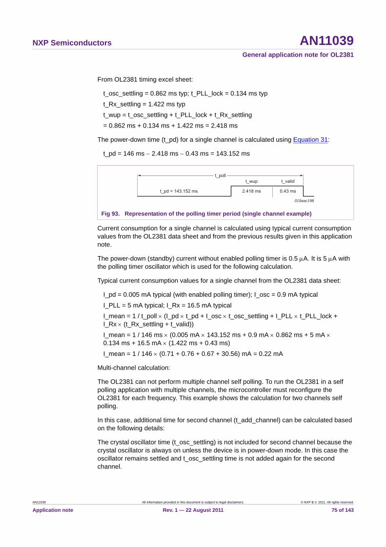
NXP Semiconductors AN11039General application note for OL2381
From OL2381 timing excel sheet:
t_osc_settling = 0.862 ms typ; t_PLL_lock = 0.134 ms typ
t_Rx_settling = 1.422 ms typ
t_wup = t_osc_settling + t_PLL_lock + t_Rx_settling
= 0.862 ms + 0.134 ms + 1.422 ms = 2.418 ms
The power-down time (t_pd) for a single channel is calculated using Equation 31:
t_pd = 146 ms 2.418 ms 0.43 ms = 143.152 ms
Current consumption for a single channel is calculated using typical current consumption values from the OL2381 data sheet and from the previous results given in this application note.
The power-down (standby) current without enabled polling timer is 0.5 A. It is 5 A with the polling timer oscillator which is used for the following calculation.
Typical current consumption values for a single channel from the OL2381 data sheet:
I_pd = 0.005 mA typical (with enabled polling timer); I_osc = 0.9 mA typical
I_PLL = 5 mA typical; I_Rx = 16.5 mA typical
I_mean = 1 / t_poll (I_pd t_pd + I_osc t_osc_settling + I_PLL t_PLL_lock + I_Rx (t_Rx_settling + t_valid))
I_mean = 1 / 146 ms (0.005 mA 143.152 ms + 0.9 mA 0.862 ms + 5 mA 0.134 ms + 16.5 mA (1.422 ms + 0.43 ms)
I_mean = 1 / 146 (0.71 + 0.76 + 0.67 + 30.56) mA = 0.22 mA
Multi-channel calculation:
The OL2381 can not perform multiple channel self polling. To run the OL2381 in a self polling application with multiple channels, the microcontroller must reconfigure the OL2381 for each frequency. This example shows the calculation for two channels self polling.
In this case, additional time for second channel (t_add_channel) can be calculated based on the following details:
The crystal oscillator time (t_osc_settling) is not included for second channel because the crystal oscillator is always on unless the device is in power-down mode. In this case the oscillator remains settled and t_osc_settling time is not added again for the second channel.
Fig 93. Representation of the polling timer period (single channel example)
019aac198
t_pd = 143.152 ms
t_poll
2.418 ms 0.43 ms
t_wup t_valid
AN11039 All information provided in this document is subject to legal disclaimers. © NXP B.V. 2011. All rights reserved.
Application note Rev. 1 — 22 August 2011 75 of 143

NXP Semiconductors AN11039General application note for OL2381
The PLL lock time (t_PLL_lock) excludes the VCO and PLL regulators ready time. The new PLL lock time includes only VCO calibration, lock detector switching time and time for PLL signal locking.
Therefore the additional time for second channel (t_add_channel) is calculated as follows:
t_add_channel = t_PLL_lock_C2 + t_Rx_settling + t_valid
t_PLL_lock_C2 is the PLL lock time for the second channel while the t_Rx_settling and t_valid times for the second channel are the same as for the first channel.
t_PLL_lock_C2 = t_VCO calibration + t_lock detector switching + t_PLL signal lock
From the OL2381 excel sheet:
t_PLL_lock_C2 = 0.068 ms + 0.025 ms + 0.032 ms = 0.125 ms
t_add_channel = t_PLL_lock_C2 + t_Rx_settling + t_valid
t_add_channel = 0.125 ms + 1.422 ms + 0.43 ms = 1.977 ms
Polling timer period, wake up time, and data validation time are the same for single channel and multi-channel applications. Power-down time is changed for additional time (t_additional_channel).
Power-down time for two channels is calculated as follows:
t_pd_multi = t_poll t_wup t_valid t_add_channel
t_pd_multi = 146 ms 2.418 ms 0.43 ms 1.977 ms = 141.175 ms
Typical current consumption calculation (two channels example):
I_mean_multi = 1 / t_poll (I_pd t_pd_multi + I_osc t_osc_settling + I_PLL t_PLL_lock_C1 + I_Rx (t_Rx_settling + t_valid) + I_PLL t_PLL_lock_C2 + I_Rx (t_Rx_settling + t_valid))
t_PLL_lock_C1 = 0.134 ms (PLL lock value for first channel)
t_PLL_lock_C2 = 0.125 ms (PLL lock value calculated for additional channel)
t_pd_multi = 141.175 ms
I_mean_multi = 1 / 146 ms (0.005 mA 141.175 ms + 0.9 mA 1.012 ms + 5 mA 0.134 ms + 16.5 mA (1.422 ms + 0.43 ms) + 5 mA 0.125 ms + 16.5 mA (1.422 ms + 0.43 ms)
I_mean_multi = 1 / 146 (0.71 + 0.91 + 0.67 + 30.56 + 0.625 + 30.56) mA = 0.438 mA
If the OL2381 is configured by the microcontroller for polling on more frequencies, a similar procedure for polling timer period and current consumption can be followed.
Fig 94. Representation of the polling timer period (two channels example)
019aac284
t_pd_multi = 141.175 ms
t_poll
2.418 ms 0.43 ms
t_wup t_valid
1.977 ms
t_add_channel
AN11039 All information provided in this document is subject to legal disclaimers. © NXP B.V. 2011. All rights reserved.
Application note Rev. 1 — 22 August 2011 76 of 143

NXP Semiconductors AN11039General application note for OL2381
The power-down and additional channel time for “n” channels can be calculated as follows:
t_add_nchannels = n (t_add_channel) additional time for “n” channels
t_pd_nchannels = t_ poll t_wup t_valid t_add_nchannels pd time for “n” chan.
7.2 Receiver analog module
The OL2381 analog RF receiver front-end consists of an LNA, mixer, channel filter and limiter.
The receiver matching circuit transforms the OL2381 LNA single-ended input impedance into 50 at the desired operating frequency. This maximizes the power transfer and minimizes the noise figure of the receiver.
7.2.1 Receive matching
When the OL2381 demoboard is used for correct transmit/receive selection by RF, control logic bits P14C in register PORTCON2 (address: 0x12) should be set to 11 as shown in Figure 43 on page 39.
Proper receive matching can be checked by measuring the S11 parameter of the receiver LNA at 434 MHz with a network analyzer as shown in Figure 95.
The receiver matching is close to 50 , the best achievable with standard available values for passive components (L, C) on the market. The different values of receive matching for different frequencies are presented in Figure 95 and Figure 96.
Fig 95. Smith chart of the S11 receiver input into matching network 434 MHz
019aac199
0.2
0.5
1
2
5
0.2
0.5
1
2
5
10
10
0 50.50.2 21 10+j
-j∞
Mkr1
AN11039 All information provided in this document is subject to legal disclaimers. © NXP B.V. 2011. All rights reserved.
Application note Rev. 1 — 22 August 2011 77 of 143

NXP Semiconductors AN11039General application note for OL2381
The LNA output is internal to the IC. It is not accessible and can not be monitored.
The OL2381 test pins TEST1 and TEST2 can be used to monitor the operation of various blocks in the receive chain. By setting ANA_TEST_SEL bits in register TEST1 (address: 0x36) either mixer, or channel filter, or limiter test buffer outputs can be activated as shown in Figure 97 and Figure 27. Register TEST1 controls the outputs of these test buffers. The OL2381 demoboard has connectors with names matching OL2381 pins TEST1 and TEST. These pins should be monitored with a high-impedance probe.
During test mode the current consumption of the OL2381 increases by a few mA. During regular receive operation the 3 bits of ANA_TEST_SEL should be set to logic 0.
In order to start evaluating different receiver analog blocks, the Carrier Wave (CW) signal at 434 MHz and 90 dBm of power should be applied from the signal generator to the RF connector of the demoboard.
Fig 96. Receive matching components for 434 MHz
Table 26. Receive matching; component values and results
Frequency C30 (pF) L5 (nH) C12 (pF) Current (mA)
315 MHz 100 39 5.6 17
434 MHz 56 27 4.7 17
868 MHz 56 11 1.8 17
Fig 97. Register TEST1
Table 27. Functionalities of bits ANA_TEST_SEL in register TEST1
ANA_TEST_SEL Analog test function at ports TEST1 and TEST2
00 disabled (high-Z)
01X limiter I and Q output
100 mixer output
101 channel filter output
110 limiter output
111 reserved
019aac200
C30
56 pF
C12
4.7 pF
L527 nH
OL2381 RX
GND
019aac201
AN11039 All information provided in this document is subject to legal disclaimers. © NXP B.V. 2011. All rights reserved.
Application note Rev. 1 — 22 August 2011 78 of 143

NXP Semiconductors AN11039General application note for OL2381
7.2.2 Low-noise amplifier
The LNA has adjustable gain (typically 4 dB to 25.5 dB). The gain can be set in either via the receive command or register RXGAIN (address: 0x21). Figure 98 shows the gain mode setting of register RXGAIN.
Bits 6 and 7 in register RXGAIN set the LNA value to “high gain mode”, and bits 3 and 2 set the LNA value to “low gain mode”. By setting bits 6 and 7 (or 2 and 3) four different gain settings (4 dB to 25 dB) can be chosen as explained in the OL2381 data sheet.
Bits E and F in the receive command (Table 25 on page 69 and Figure 86 on page 69) are used to select the LNA mode: “high gain” or “low gain”, for example, if these bits are set to 11, the setting of bits RX_HI_GAIN in register RXGAIN are used. If these bits are set to 10, the setting of bits RX_LOW_GAIN in register RXGAIN are used.
7.2.3 Mixer
The mixer is realized as an active IQ mixer which should provide good image rejection at 434.6 MHz. It has a typical voltage conversion gain of 4 dB.
7.2.4 Channel filter
The channel filter is an RC type poly-phase 4th-order filter. Filter gain and bandwidth can be selected independently with control bits. Filter gain is set with bits 0, 1, 4 and 5 in register RXGAIN (address: 0x21).
The filter bandwidth can be configured by setting CF_BW bits[6:4] in register RXBW (address: 0x22) shown in Figure 99.
The configuration of the channel filter bandwidth (50 kHz to 300 kHz) is shown in the OL2381 data sheet.
Channel filter output without RF signal applied at the input can be monitored with a spectrum analyzer as shown in Figure 100 where the LNA and channel filter are in high gain mode. Different channel filter bandwidths are shown from 300 kHz to 50 kHz in Figure 101.
Fig 98. Register RXGAIN
019aac202
Fig 99. Register RXBW for configuring the channel filter
019aac203
AN11039 All information provided in this document is subject to legal disclaimers. © NXP B.V. 2011. All rights reserved.
Application note Rev. 1 — 22 August 2011 79 of 143

NXP Semiconductors AN11039General application note for OL2381
Channel filter outputs (I and Q) with a carrier wave (CW) signal applied at the input can also be monitored with an oscilloscope as shown in Figure 101.
Fig 100. Channel filter output
019aac204
AN11039 All information provided in this document is subject to legal disclaimers. © NXP B.V. 2011. All rights reserved.
Application note Rev. 1 — 22 August 2011 80 of 143

NXP Semiconductors AN11039General application note for OL2381
The bandwidth of the channel filter should be chosen carefully. In order to achieve the best signal-to-noise performance of the receiver it should be as close as possible to the bandwidth occupied by the modulated receive signal. If the bandwidth is chosen too wide, a large amount of noise is passed through the filter reducing the signal-to-noise ratio of the receiver. If the bandwidth is set too narrow, some data will be missed degrading the bit error rate measurement (receiver sensitivity).
In general, the channel filter bandwidth should be set according to the Carson’s rule where the bandwidth is equal to twice the sum of modulating frequency and frequency deviation. An example of a bad choice of filter bandwidth is shown in for a bandwidth that is too wide (300 kHz) in Figure 102 and too narrow (50 kHz) in Figure 103. Modulation frequency is 20 kHz, and deviation is 40 kHz.
Fig 101. Channel filter outputs I and Q
Fig 102. Channel filter output with a 300 kHz channel filter bandwidth
019aac205
019aac206
AN11039 All information provided in this document is subject to legal disclaimers. © NXP B.V. 2011. All rights reserved.
Application note Rev. 1 — 22 August 2011 81 of 143

NXP Semiconductors AN11039General application note for OL2381
An auto-calibration of the channel filter is performed automatically before every receive operation. It should compensate for the process and temperature dependant parameters in the filter. The four CF_RC_CAL_RES bits in register CFRCCAL (address: 0x2F), shown in Figure 104, indicate the result of the channel RC calibration and they are directly applied to the internal RC components of the filter. RC calibration can be blocked by setting bit SKIP_CF_RC_CAL of register TEST4 (address: 0x39), and forced by setting bit FORCE_CF_RC_CAL in the same register. This register is shown in Figure 105. In normal operation these two bits are set to logic 0.
If RC calibration is omitted, the output of the channel filter should be as shown in Figure 106. By setting bits MAN_CF_RC_CALVAL in register TEST4 to the same values as bits CF_RC_CAL_RES in Figure 104, the channel filter output should be a flat response.
Fig 103. Channel filter output with a 50 kHz channel filter bandwidth
Fig 104. Register CFRCAL
Fig 105. Register TEST4
019aac207
019aac208
019aac209
AN11039 All information provided in this document is subject to legal disclaimers. © NXP B.V. 2011. All rights reserved.
Application note Rev. 1 — 22 August 2011 82 of 143

NXP Semiconductors AN11039General application note for OL2381
The image frequency rejection (in this case 434 MHz + 600 kHz = 434.6 MHz) is one of the most important receiver parameters. The matching of the amplitude and phase of I and Q channels affects the image rejection. The IQ calibration enables the receiver to adjust internal gains of I and Q channels.
A signal at the image frequency should be applied to the receiver, and the level of the signal should be chosen in a way that the Received Signal Strength Indication ratio (RSSI) circuit is still able to measure the image signal. The IQ calibration is enabled by setting bit START_CF_IQ_CAL in register CFIQCAL (address 0x48). All possible offset combinations are run and RSSI measurement is performed. The combination with the minimum RSSI reading is stored in bits CF_IQ_CALVAL in register CFIQCAL. This information needs to be stored in an external microcontroller. Register CFIQCAL is shown in Figure 107. After setting a certain CF_IQ_CALVAL value, a waiting time of about 300 s is needed until the new RSSI value can be processed. The IQ calibration depends on the setting of bits RSSI_FILTER_FC and CFBW in register RXBW.
By performing IQ calibration, image rejection improves by about 5 dB and image rejection should be higher than 50 dBc.
7.2.5 Limiter
The next block in the receive chain is the limiter. It amplifies its input signal while ensuring its output signal stays constant. It consists of 5 gain stages per I and Q channel.
When the CW signal at 434 MHz and 90 dBm of power is applied from the signal generator to the RF connector of the demoboard, the limiter output is shown in Figure 108 and Figure 109. LNA and channel filter are in high gain mode.
Fig 106. Channel filter output when RC calibration is omitted
Fig 107. Register CFIQCAL
019aac210
019aac211
AN11039 All information provided in this document is subject to legal disclaimers. © NXP B.V. 2011. All rights reserved.
Application note Rev. 1 — 22 August 2011 83 of 143

NXP Semiconductors AN11039General application note for OL2381
7.2.6 RSSI
The analog outputs of the limiter gain stages are used with the RSSI block to measure the received signal strength on a logarithmic scale. The RSSI level is proportional to the input level. The RSSI result can be seen in register RSSILEVEL (address 0x39) shown in Figure 110. Bit STATAUTOSAMPLE in register RXCON (address: 0x53) must be set to obtain a correct RSSI reading in register RSSILEVEL; see Figure 111.
Fig 108. Limiter output for a CW signal at 434 MHz and 90 dBm
Fig 109. Limiter output signal at pins TEST1 and TEST2 (signaIs I and Q)
019aac212
019aac213
Fig 110. Register RSSILEVEL
019aac214
AN11039 All information provided in this document is subject to legal disclaimers. © NXP B.V. 2011. All rights reserved.
Application note Rev. 1 — 22 August 2011 84 of 143

NXP Semiconductors AN11039General application note for OL2381
The receiver requires a wide dynamic range for ASK demodulation and carrier detection. Automatic gain control (AGC) is used for this purpose. Figure 112 shows the RSSI characteristic as a function of input power level. The green curve shows the RSSI characteristic in low gain mode, and the red curve shows the RSSI characteristic in high gain mode. Each of these two modes has a dynamic range of about 70 dB. Depending on the switching point between these two modes, the overall receiver dynamic range should be higher than 100 dB.
A compensation value can be set in register GAINSTEP (address. 0x23) as shown in Figure 113 in order to achieve a continuous RSSI reading when the gain setting of the front-end is changed. The register value is the difference in the RSSI readings (in the linear region) for the same input power between high and low gain mode. This value is added to the RSSI result when the low gain is activated. This seamlessly extends an overall dynamic range of the receiver to higher than 100 dB.
Fig 111. Register RXCON
Fig 112. RSSI characteristic as a function of input power level
Fig 113. Register GAINSTEP
019aac215
019aac216
switch
40 dB switch of gain in LNA
1.65
1.00
+ 65 %
RSSI
Pi (dBm)-120 -70 -20-40-100
019aac217
AN11039 All information provided in this document is subject to legal disclaimers. © NXP B.V. 2011. All rights reserved.
Application note Rev. 1 — 22 August 2011 85 of 143

NXP Semiconductors AN11039General application note for OL2381
The default setting for the receiver is high gain mode. As soon as the level at the input is high enough, the gain of the LNA and channel filter is lowered to increase the receiver’s linearity and dynamic range. The RSSI information can also be used to reduce the output power for transmit operation.
Information about the switching point between high and low gain mode is stored in register HIGAINLIM (address: 0x24), shown in Figure 114. As explained earlier, the default setting for the receiver is high gain mode. At power-up, if gain switching is enabled during wake-up search, shown in Figure 86 on page 69 (receive command bits 2 and 3 set to 01) and HI_GAIN_LIMIT in register HIGHGAINLIM is exceeded by the RSSI level in register RSSILEVEL, the receiver switches automatically to low gain mode.
The RC analog filter is used to achieve a more stable digital RSSI reading. This low-pass filter can be trimmed by bits CAPRSSI in register EXPERT2 (address: 0x33) shown in Figure 115.
The RSSI value is fed to a digital filter where the digital RSSI filter cut-off frequency can be set by bits RSSI_FILTER_FC in register RXBW as shown in Figure 99 on page 79.
The main role of the RSSI circuit in the receiver chain is signal level detection, which differentiates noise, unwanted disturbers and wanted receive signal. Only a few different scenarios are supported for this. More details are given in the OL2381 data sheet. The following example explains the scenario where the carrier signal strength is supposed to be between a given minimum and maximum value, and the presence of the carrier is determined.
Figure 116 shows registers LOWERRSSITH (address: 0X26) and UPPERRSSITH (address: 0X25) which show the lower and upper limits of the desired RSSI range.
Fig 114. Register HIGAINLIM
Fig 115. Register EXPERT2
019aac218
019aac219
AN11039 All information provided in this document is subject to legal disclaimers. © NXP B.V. 2011. All rights reserved.
Application note Rev. 1 — 22 August 2011 86 of 143

NXP Semiconductors AN11039General application note for OL2381
Figure 117 shows the status registers SIGMONSTATUS (address: 0X37), SIGMONERROR (address: 0X38), and RSSI_LEVEL (address: 0X39) which are used for signal monitoring. The status is sampled at the end of a wake-up search and preamble detection, and after a Read command if bit STATAUTOSAMPLE is set; see Figure 111 on page 85. Bits 2 in registers SIGMONSTATUS and SIGMONERROR are respectively RSSI check valid and RSSI check error. The RSSI signal monitor fail occurs when the RSSI_LEVEL (Figure 117) is outside the range shown in Figure 116 (37 is not between 40 and 120). In this case, RSSI check valid and RSSI check error bits will be set to logic 1 as shown in Figure 117 and they will indicate that RSSI is out of range. Register EXTRXSTATUS (address: 0x2E) samples registers SIGMONSTATUS, SIGMONERROR and RSSILEVEL to check the status.
7.3 Receiver digital module
The digital debug board from the design-in-kit is used to observe the digital signals of the OL2381. Further details of this board are explained in the user manual of the design-in-kit board.
Fig 116. Registers UPPERRSSITH and LOWERRSSITH
Fig 117. Signal monitoring configuration
019aac220
019aac221
AN11039 All information provided in this document is subject to legal disclaimers. © NXP B.V. 2011. All rights reserved.
Application note Rev. 1 — 22 August 2011 87 of 143

NXP Semiconductors AN11039General application note for OL2381
The IF output of the limiter interfaces the signal which enters the digital circuit. All further processing (FM demodulation, baseband filtering, clock recovery, etc.) is performed in the digital domain.
The simplified block diagram of the receiver digital module is shown in Figure 118.
This section presents important register settings for various blocks, some important application aspects and signals where they are accessible.
The OL2381 initiates receive mode by sending the receive command as shown in Figure 86 on page 69. Setting the receive command bits C and D to 11 sets the receiver to data reception without preamble detection mode. This command always uses DATACON set as the dynamic configuration for the slicer and signal detection and classification methods. After initializing the slicer, it behaves like the PRDA command (receive command bits C and D set to 10) after successful preamble detection. To set up a PRDA command, bits C and D in Figure 86 on page 69 must be set to 10.
Table 28 presents the dynamic configuration sets.
Different receive modes and dynamic receiver configurations are explained in detail in the OL2381 data sheet and are described later. This document will use data reception without preamble detection receiver mode to show some important application aspects.
Fig 118. Receiver digital part block diagram
019aac222
I limiter
Q limiter
6 RSSI bitsfrom ADC
DIGITALFM
DEMODULATOR
ASK/FSKSLICER CLOCK
RECOVERY
PREAMBLEDETECTION
SYNCHRONISATIONAND
DECODING
TIMINGCHECK
BITRATECHECK
CODINGCHECK
DE-GLITCHER
transparent data
transparent clock
data
clock
CL
D
RSSI LOGICANALOG SIGNAL
MONITORSCALING
MODAMPSIGNAL
MONITOR
basebandfilter
digitalRSSIfilter
Table 28. Dynamic receiver configuration sets
Dynamic configuration WUPSCON PREACON DATACOM
NUM_MODAMP_GAPS NUM_MODMP_GAPS_W NUM_MODAMP_GAPS_P NUM_MODAMP_GAPS_D
SLICERSEL SLICERSEL_W SLICERSEL_P SLICERSEL_D
SLICERINITSEL SLICERINITSEL_W SLICERINITSEL_PD
INIT_ACQ_BITS INIT_ACQ_BITS INIT_ACQ_BITS_PD
CODINGRESTR CODINGRESTR_W CODINGRESTR_P CODINGRESTR_D
SIGMON_EN SIGMON_EN_W SIGMON_EN_P SIGMON_EN_D
AN11039 All information provided in this document is subject to legal disclaimers. © NXP B.V. 2011. All rights reserved.
Application note Rev. 1 — 22 August 2011 88 of 143

NXP Semiconductors AN11039General application note for OL2381
7.3.1 Digital FM demodulator
The input to the digital module of the receiver is the limited IF I signal and optionally also the Q signal. There are no visible advantages of using both I and Q channels for demodulation.
The following option is available in register EXPERT2; see Figure 115 on page 86. If bit FM_DEM_IANDQ is set to logic 0 only the I channel is used in FM demodulator. The OL2381 is specified to operate at a frequency deviation up to 100 kHz which means that the FM demodulator input frequency range should be 200 kHz to 400 kHz. However, in some applications by setting bit LARGE_FM_DEM_RANGE to logic 1 (logic 0 is the appropriate setting for 100 kHz maximum deviation) the input frequency range can be extended from 0 Hz to 600 kHz. This allows the processing of higher frequency deviations, limited only by the bandwidth of the analog channel filter. If the FM demodulator input frequency is between 200 kHz and 400 kHz, its output is a perfectly linear function of the input frequency and the OL2381 would comply to its receive specification.
7.3.2 Digital test interface
The type of demodulation used by the receiver is selected in register RXBW (address: 0x22) shown in Figure 99 on page 79. If ASK demodulation is used bit 7 DEMOD_ASK should be set to 1. Default is FSK demodulation which is set by the value of 0. So by sending the receive command as shown in Figure 86 on page 69 the receiver will try to demodulate ASK or FSK signal depending on the choice of the DEMOD_ASK bit. Some other registers need to be set as well for correct demodulation.
Setting bits RXD-DBG-SEL in register TEST0 (address: 0x35), shown in Figure 119, to a non-zero value, switches ports P10/DATA, P11/INT and P12/CLOCK to receiver digital debug mode.
In this mode the normal pin functions of P10/DATA, P11/INT and P12/CLOCK are overwritten with the functions of a fast 3-wire synchronous serial transmission which signals when various digital blocks in the receiver can be monitored. Register bits RXD-DBG-SEL determine which 16-bit signal vector is sampled with 1 Msample/s and outputs serially. A table of the list of all available debug signal vectors is shown in the OL2381 data sheet. P10 outputs the serial data, P12 outputs 16 MHz serial clock, and P11 outputs a frame pulse for each serial 16-bit word.
In order to use the digital debug interface for signal monitoring and debugging, the digital debug board should be used. The correct operation of this synchronous interface can be checked by connecting oscilloscope probes to Data, CLK and INT test pins on the RF board. The signal format should be similar to that shown in Figure 120.
Fig 119. Register TEST0
019aac223
AN11039 All information provided in this document is subject to legal disclaimers. © NXP B.V. 2011. All rights reserved.
Application note Rev. 1 — 22 August 2011 89 of 143

NXP Semiconductors AN11039General application note for OL2381
The three traces are clock, data, and frame, respectively. If the format of the digital test signal is similar to Figure 120, the on-board (digital debug board) serial-to-parallel converter makes the test signal vector, selected by bits RXD-DBG-SEL, available at the digital debug board jumper row. If the jumpers for the 12 MSBits of the jumper row are connected, the output of the test signal vector selected by bits RXD-DBG-SEL will be sent to the on-board (digital debug board) Digital-to-Analog Converter (DAC) for further conversion to an analog voltage.
7.3.3 Baseband filter
If the OL2381 is configured for receive mode at 434 MHz and a CW signal of 434 MHz at 70 dBm is applied to the OL2381 receiver input, the DAC output should be a noise-free DC voltage of about 1.32 V. This is the baseband filter output (test vector #4) which corresponds to an IF of exactly 300 kHz. If the input frequency is varied in 10 kHz steps, the DAC output voltage should follow the changes in the opposite direction.
The effect of selecting the correct channel filter bandwidth is already shown in Section 7.2.4 on page 79. It can also be selected using the digital debug interface. If a 434 MHz modulation signal of 70 dBm input level with 90 kHz frequency deviation, 100 Hz triangle wave frequency is applied to the OL2381 receiver input, the baseband filter output (test vector #4 is selected) should be identical to the signal shown in Figure 121.
Fig 120. Digital test interface format
019aac224
AN11039 All information provided in this document is subject to legal disclaimers. © NXP B.V. 2011. All rights reserved.
Application note Rev. 1 — 22 August 2011 90 of 143
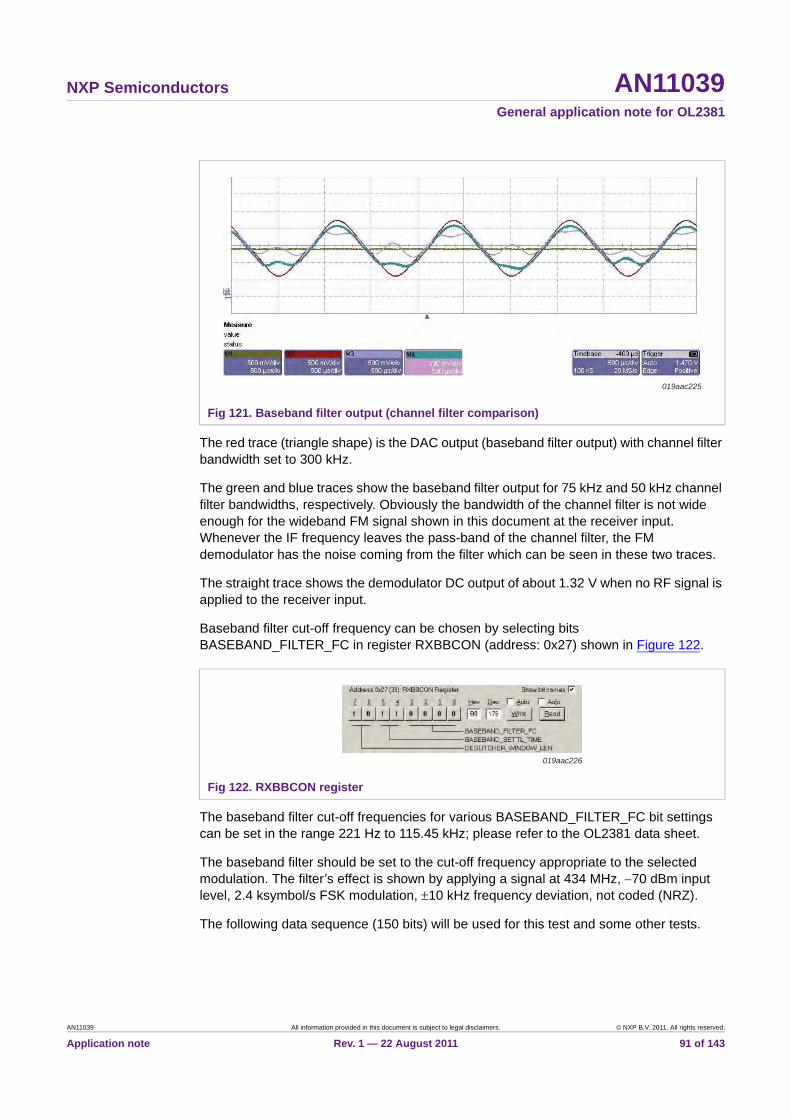
NXP Semiconductors AN11039General application note for OL2381
The red trace (triangle shape) is the DAC output (baseband filter output) with channel filter bandwidth set to 300 kHz.
The green and blue traces show the baseband filter output for 75 kHz and 50 kHz channel filter bandwidths, respectively. Obviously the bandwidth of the channel filter is not wide enough for the wideband FM signal shown in this document at the receiver input. Whenever the IF frequency leaves the pass-band of the channel filter, the FM demodulator has the noise coming from the filter which can be seen in these two traces.
The straight trace shows the demodulator DC output of about 1.32 V when no RF signal is applied to the receiver input.
Baseband filter cut-off frequency can be chosen by selecting bits BASEBAND_FILTER_FC in register RXBBCON (address: 0x27) shown in Figure 122.
The baseband filter cut-off frequencies for various BASEBAND_FILTER_FC bit settings can be set in the range 221 Hz to 115.45 kHz; please refer to the OL2381 data sheet.
The baseband filter should be set to the cut-off frequency appropriate to the selected modulation. The filter’s effect is shown by applying a signal at 434 MHz, 70 dBm input level, 2.4 ksymbol/s FSK modulation, 10 kHz frequency deviation, not coded (NRZ).
The following data sequence (150 bits) will be used for this test and some other tests.
Fig 121. Baseband filter output (channel filter comparison)
Fig 122. RXBBCON register
019aac225
019aac226
AN11039 All information provided in this document is subject to legal disclaimers. © NXP B.V. 2011. All rights reserved.
Application note Rev. 1 — 22 August 2011 91 of 143

NXP Semiconductors AN11039General application note for OL2381
Figure 124 shows the signal of the baseband filter output when test vector #4 is selected.
The three traces were taken with the three most appropriate settings for a baseband filter for 2.4 ksymbol/s. The cut-off frequency for the green trace is 3540 Hz, for the red trace is 1770 Hz, and for the blue trace is 885 Hz. The filter with a cut-off frequency of 1770 Hz is the optimum in this case whereas a filter with a cut-off frequency of 885 Hz attenuates more high frequency components. If the input signal to the receiver is changed by 1 kHz, the baseband signal DC component varies with the center frequency in the opposite direction.
7.3.4 Data slicer
The OL2381 has an edge-sensitive slicer and a level-sensitive slicer.
• The level-sensitive slicer is more robust to noise, but needs longer settling time making it the recommended choice for ASK demodulation
• The edge-sensitive slicer should be used in applications where a fast settling time is crucial making it the recommended choice for FSK demodulation
• The edge slicer is capable of demodulating NRZ code with long constant bit sequences providing that the expected peak modulation amplitude is initialized correctly
However, both types of slicer can be used for both modulation types.
Fig 123. Data sequence for test
Fig 124. Baseband filter output (baseband filter comparison)
019aac227
0101 0101 0101 0101 0101 0101 0101 0101
1001 1001 1010 0101 1010 1011 1010 1101
0011 0111 1011 0100 1101 0101 1011 0110
1011 0110 1101 1000 0111 1011 1100 1010
1101 1011 1011 0101 0101 01
019aac228
AN11039 All information provided in this document is subject to legal disclaimers. © NXP B.V. 2011. All rights reserved.
Application note Rev. 1 — 22 August 2011 92 of 143

NXP Semiconductors AN11039General application note for OL2381
The edge and level slicer differ on two points: the time to obtain correct data and the delay. The edge slicer takes only one chip period to be correctly set. The level slicer needs 4 or 16 chip periods. But when the level slicer is "locked" to the data (no errors), there is no delay. The edge slicer needs five adjacent samples which automatically induces a delay of one chip period. If the level slicer is pre-initialized with the correct threshold, the lost bits can be recovered.
The slicer to be used in the receiver is set by registers RXDCON0, RXDCON1, and RXDCON2 (addresses: 0x2B, 0x2C, and 0x2D).
Since data reception without preamble detection receiver mode is used for evaluating the receiver, the relevant bits are SLICERSEL_D in the register shown in Figure 125.
In the digital debug interface there is no available signal vector for the edge-sensitive slicer threshold. However, vector #6 is available which represents the threshold of the level-sensitive slicer and its operation is explained with some examples.
7.3.4.1 Level-sensitive slicer
Bits SLICERSEL_D and SLICERINITSEL_PD should be set to 11 for level-sensitive slicer operation as shown in Figure 125.
The level-sensitive slicer loads the initialization value which is stored in the 15-bit SLICERINITTHR of registers SLICERINITL (address: 0x32) and SLICERINITH (address: 0x33). The bit values adjust the threshold continuously to the received signal and compare the baseband signal output with the dynamic threshold SLICERTHR.
A vector signal generator is used to demonstrate the operation of the level-sensitive slicer. The following signal is applied to the receiver input: 434 MHz, 70 dBm input level, 2.4 ksymbol/s FSK modulation, 2 kHz frequency deviation. The same 150 bits data sequence as in Figure 123 on page 92 is applied to the receiver input.
Figure 126 shows some control signals used in the vector signal generator: Burst gate, Level attenuation, CW Mod, and Marker 1. Burst gate LOW shuts off the RF signal. CW Mod HIGH switches off the modulating signal. Level attenuation HIGH attenuates the signal. Marker 1 triggers the oscilloscope and spectrum analyzer.
Fig 125. RXDCON1 and RXDCON2 registers
019aac229
AN11039 All information provided in this document is subject to legal disclaimers. © NXP B.V. 2011. All rights reserved.
Application note Rev. 1 — 22 August 2011 93 of 143

NXP Semiconductors AN11039General application note for OL2381
Figure 127 shows three oscilloscope traces when test vector #4 is selected: modulated data input (green trace), channel filter output (red trace), and baseband output signal (yellow trace). When no RF signal applied, the baseband output signal shows high random noise as shown in the middle of the plot. Then there is a short interval with an attenuated RF signal applied without modulation. It is shown as a constant line (DC value) followed by another constant line with higher amplitude. It represents a non-attenuated RF signal without modulation. After that follows a successfully demodulated, filtered signal. The channel filter output signal for the same time interval shows only noise passing through the filter, attenuated output, and normal output.
Figure 128 presents the modulated signal in the time domain with zero span used. This can be monitored on the spectrum analyzer. LOW level shows no RF signal applied, constant line represents non-modulated signal applied with and without attenuation followed by modulated signal.
Fig 126. Control signals
Fig 127. Modulated signal, channel filter and baseband output observed on the oscilloscope
019aac230
019aac231
AN11039 All information provided in this document is subject to legal disclaimers. © NXP B.V. 2011. All rights reserved.
Application note Rev. 1 — 22 August 2011 94 of 143

NXP Semiconductors AN11039General application note for OL2381
Finally, in Figure 129 three traces are shown: green trace: baseband filter output (test vector #4 selected), brown trace: level-slicer threshold (test vector #6 selected), and blue trace: representing slicer output (test vector #8 selected, bit 7). Baseband filter output and slicer output can not be monitored simultaneously because only one vector can be selected at the digital debug interface. Marker 1 control signal is used for triggering the oscilloscope and two sweeps have been made. Figure 129 is the best explanation of how the level-slicer works.
The following examples show possible problems in real applications. If the transmitted signal (434.03 MHz) is shifted for 30 kHz with respect to the receiver frequency setting (434 MHz), the data slicer threshold settling time is much longer. It would cause some “lost” bits at the beginning of the sequence as shown in Figure 130. This is a clear example of how the tolerance of the crystal oscillator both in the transmitter and receiver are important. The baseband filter output, slicer threshold and slicer outputs are shown in Figure 130.
Fig 128. Modulated signal in time domain at the spectrum analyzer
Fig 129. Baseband filter output, level slicer threshold and level slicer output
019aac232
019aac233
AN11039 All information provided in this document is subject to legal disclaimers. © NXP B.V. 2011. All rights reserved.
Application note Rev. 1 — 22 August 2011 95 of 143

NXP Semiconductors AN11039General application note for OL2381
The next application example is the presence of the long sequence of “1s” or “0s” in the modulated non-coded (NRZ) signal shown in Figure 131. Red and dark blue traces show the baseband signal output (test vector #4 selected) and level-slicer threshold (test vector #6 selected). Green and light blue traces show the modulated signal and slicer output (test vector #8 selected, bit 7). A long sequence of ones at the receiver input causes many “lost” bits. This can be prevented by using Manchester coding which is implemented in the OL2381. However, this would double the symbol rate and increase the bandwidth. It is recommended to use an OL2381 encoding which guarantees a maximum of 6 matching consecutive bits.
The next application example shows the presence of a close frequency CW interferer signal. Figure 132 and Figure 133 show the effect of a 434.02 MHz CW interferer at an input level of 50 dBm that is identical to the wanted signal. Green and red traces show the baseband filter output and slicer threshold when the interferer is switched off. The dark and light blue indicate the baseband filter output and slicer threshold when the interferer is on. Obviously when the interferer is present there is no usable demodulated data.
Fig 130. Baseband filter output, slicer threshold, and slicer output for frequency offset signal
Fig 131. Baseband filter output, slicer threshold, and slicer output for long “1” sequence
019aac234
019aac235
AN11039 All information provided in this document is subject to legal disclaimers. © NXP B.V. 2011. All rights reserved.
Application note Rev. 1 — 22 August 2011 96 of 143

NXP Semiconductors AN11039General application note for OL2381
Furthermore, if the interferer is modulated, the receiver would demodulate an unwanted signal during the time when the wanted signal is off as represented on the left side of the plot.
Figure 134 and Figure 135 show the effect of an interferer at 434.02 MHz with an input level of -51 dBm (1 dB lower). Red and green traces show the baseband filter output and slicer threshold when the interferer is switched off, and two blue traces show the baseband filter output and slicer threshold when the interferer is on. When the near frequency interferer with just 1 dB less power is present, the OL2381 is still able to demodulate the wanted signal.
Fig 132. Baseband filter output and slicer threshold: interferer with the same power present
Fig 133. Baseband filter output and slicer output: interferer with the same power present
019aac236
019aac237
AN11039 All information provided in this document is subject to legal disclaimers. © NXP B.V. 2011. All rights reserved.
Application note Rev. 1 — 22 August 2011 97 of 143

NXP Semiconductors AN11039General application note for OL2381
The slicer output is further processed in the de-glitcher, clock recovery, and synchronization and decoding blocks. These blocks are not accessible via the digital debug interface and are described in detail in the OL2381 data sheet.
7.3.5 De-glitcher
The purpose of the de-glitcher is to suppress multiple signal transitions when a noisy baseband signal crosses the slicer threshold. If a signal transition is detected, the de-glitcher passes the transition to its output and then locks this output for a certain time period, which can be selected with bits DEGLITCHER_WINDOW_LEN in register RXBBCON. More details are provided in the OL2381 data sheet; see Figure 122 on page 91.
7.3.6 Clock recovery for receive mode
Clock recovery (needed for receive mode) depends on the baud rate accuracy. The clock recovery circuit is able to cope with a 1 % tolerance to be able to operate correctly with standard crystal tolerances. The clock recovery is implemented as a digital phase control
Fig 134. Baseband filter output and slicer threshold: interferer with 1 dB less power present
Fig 135. Baseband filter output and slicer output: interferer with 1 dB less power present
019aac238
019aac239
AN11039 All information provided in this document is subject to legal disclaimers. © NXP B.V. 2011. All rights reserved.
Application note Rev. 1 — 22 August 2011 98 of 143

NXP Semiconductors AN11039General application note for OL2381
loop with a fixed operating frequency (determined by the baud rate generator setting). The clock recovery PLL is programmable with regards to its settling speed. The settling of the clock recovery speed can be set to reach its final state within 3, 7, 15 or 31 chip periods. This is chosen by bits CLOCK_RECOV_TC in register RXCON; see Figure 111 on page 85. The highest settling speed (settling within 3 chips) produces the lowest phase error due to fast regulation. Slowest speed (settling within 31 chips) allows for the largest phase error due to the slowest regulation time-constant. Decoding of NRZ signals with long constant bit periods is directly influenced by the accuracy of the selected baud rate. Correct encoding (such as HDLC) can significantly improve sensitivity and the BER of NRZ decoding.
7.3.7 Signal signature recognition unit
The next block in the receive chain is the signal signature recognition unit. The purpose of this block is to provide a tool for configuring the receiver path. The main challenge in the receive mode is to distinguish the noise and unwanted disturbers from the wanted signal.
After successful detection of the wanted signal, the receive process starts. There are different units which can be individually activated and configured which are used for further recognition of the wanted signal. The OL2381 data sheet provides a table showing an overview of the signal signature recognition unit. The main blocks are: RSSI level classification, modulation amplitude classification, chip timing verification, code checker, baud rate checker, preamble detection, and WUPS timer and logic.
This section explains the RSSI level classification, modulation amplitude classification, chip timing verification, code checker, and baud rate checker, and some examples are given.
Preamble detection is explained in more detail in Section 8.1 on page 120.
The wake-up search logic and timer are explained in more detail in the OL2381 data sheet. Section 7.1 on page 68 and Section 8.2 on page 125 of this document also show some examples and block diagrams relevant to the wake-up search.
Registers SIGMON0 (WUPS), SIGMON1 (preamble detection), and SIGMON2 (data reception) provide enable bits which determine which of the signal monitor results are considered for the overall detection decision. Regardless of these enable bits, all signal monitors perform their measurements and their results are available in the corresponding status bits of register SIGMONSTATUS.
A typical application uses WUPS and Manchester encoded data. For simplicity in this section, data reception mode is used. Signal monitors for WUPS and preamble detection applications should have very similar behavior.
These signals PASS and FAIL are exclusively used for the wake-up search logic and must not be confused with the actual state of the corresponding signal monitor, i.e. signals VALID and ERROR, which can be observed at registers SIGMONSTATUS and SIGMONERROR. The examples in this section, registers SIGMONSTATUS and SIGMONERROR are only observed and an interrupt is not generated.
Registers SIGMONSTATUS and SIGMONERROR are shown in Figure 117 on page 87.
In a real application using WUPS, an interrupt request is generated at the end of the wake-up search and the result is stored in bit CMDFAIL in register SIGMONSTATUS. If this bit is set, it signals that the wake-up criteria was not met. Otherwise it is cleared.
AN11039 All information provided in this document is subject to legal disclaimers. © NXP B.V. 2011. All rights reserved.
Application note Rev. 1 — 22 August 2011 99 of 143

NXP Semiconductors AN11039General application note for OL2381
The register SIGMONSTATUS can be used as a mask for register SIGMONERROR when the host controller is interested in retrieving the cause of an unsuccessful detection.
The OL2381 provides four status registers, SIGMONSTATUS, SIGMONERROR, RSSI_LEVEL (addresses: 0x37 to 0x39) and EXTRXSTATUS (address: 0x2E) into which status information is transferred simultaneously whenever it is either actively requested by the controller, or automatically saved by the receive command execution logic.
This consistent set of status information is sampled in two cases:
• after recognition of the command code of a read command (at the second trailing edge of SCLK) only if bit STATAUTOSAMPLE in register RXCON is set,
• always at the end of a wake-up search or preamble detection
Bit STATUSAUTOSAMPLE allows the software to control whether the status is sampled with each of the following read commands (when logic 1) or whether the status is not affected by any following read command (when logic 0).
This bit is asynchronously reset to logic 0 either on master reset or whenever the receiver samples its status automatically on completion of a wake-up search or preamble detection command. This guarantees that the important wake-up search or preamble detection results are retained until they have been transferred to the controller. It is also reset to logic 0 when one of the following registers is read out: SIGMONSTATUS, SIGMONERROR, EXTRXSTATUS, but only if bit AUTOSAMPLEMANUAL, in register RXCON, is in the cleared state, which means that full automatic control of bit STATAUTOSAMPLE in register RXCON is required.
Bit STBATAUTOSAMPLE can also be automatically set to logic 1 whenever status register RSSI_LEVEL is transferred to the controller, but only if bit AUTOSAMPLEMANUAL is in the cleared state. This can be used to automatically start a new status sampling cycle after transferring the last piece of information to the controller. If this feature is used, this implies that reading one of the registers SIGMONSTATUS, SIGMONERROR or EXTRXSTATUS starts a sampling cycle and reading the register RSSI_LEVEL ends it.
This allows the handling of the following scenario: after a wake-up search or preamble detection the status is automatically sampled and stored in the status registers until the last status register (RSSI_LEVEL) has been read. The controller can then continue with polling the signal monitors without explicitly switching the status into ‘live’ mode, because reading the RSSI_LEVEL register has automatically set bit STATAUTOSAMPLE.
Registers SIGMONSTATUS and SIGMONERROR can be used to retrieve the status information of the signal monitors at the end of a wake-up search.
The bits in register SIGMONSTATUS provide the VALID information for the signal monitors. If a VALID flag is logic 0, the corresponding bit in register SIGMONERROR is also logic 0. Otherwise the bit in register SIGMONERROR delivers logic 1 if an error has occurred.
AN11039 All information provided in this document is subject to legal disclaimers. © NXP B.V. 2011. All rights reserved.
Application note Rev. 1 — 22 August 2011 100 of 143

NXP Semiconductors AN11039General application note for OL2381
If the software is only interested which signal monitor caused a FAIL, it has to only check register SIGMONERROR.
7.3.7.1 RSSI level classification
The RSSI circuit is described in Section 7.2.6 on page 84 and includes examples for setting the appropriate registers. Some RSSI signals and relevant monitors can be checked by the digital debug interface. Clock (red), data (blue) and int (green) test pins on the RF board are monitored by the oscilloscope and shown in Figure 136. The receiver input level is 70 dBm, and register RSSI_LEVEL (address: 0X39) reads 104d. A close look at these three lines between the markers (first 8 bits) show 01101000 which is 104d.
Figure 137, Figure 138, and Figure 139 show an example of how the RSSI level classification can be used in a real application. System design registers LOWERRSSITH and UPPERRSSITH (address: 0x26 and 0x25) are set to 100d and 120d; see Figure 116 on page 87.
The blue line (at top) shows the preamble marker; yellow line shows the data pin on the RF board; red line shows the RSSI signal after low-pass filter, digital debug vector 2, bits 15:4; dark blue line indicates the RSSI level is greater than the threshold set by UPPERRSSITH, digital debug vector 2, bit 2); green line indicates RSSI level is lower than the threshold set by LOWERRSSITH, vector 2, bit 1.
The RF input level is: 20 dBm for Figure 137 (indicates that RSSI level is greater than the threshold set by UPPERRSSITH when HIGH), 70 dBm for Figure 138 (both indicators are LOW), and 100 dBm for Figure 139 (indicates that RSSI level is lower than the threshold set by LOWERRSSITH when HIGH). Only the input level of 70 dBm complies with the given system requirements.
Table 29. Status information for signal monitors, SIGMONSTATUS, SIGMONERROR
SIGMONSTATUS[i] SIGMONERROR[i] Function
0 0 signal monitor in invalid phase
0 1 not possible
1 0 signal monitor did not detect an error
1 1 signal monitor detected an error
Fig 136. RSSI level for an input of 70 dBm, 104d
019aac240
clock
data 0 0 11 1 0 0 0
int
AN11039 All information provided in this document is subject to legal disclaimers. © NXP B.V. 2011. All rights reserved.
Application note Rev. 1 — 22 August 2011 101 of 143

NXP Semiconductors AN11039General application note for OL2381
Fig 137. RSSI level indicators for an input of 20 dBm
Fig 138. RSSI level indicators for an input of 70 dBm
Fig 139. RSSI level indicators for an input of 100 dBm
019aac241
Data
RSSI signalRSSI level / UPPERSSITH
RSSI level / LOWERSSITH
019aac242
Preamble marker
Data
RSSI signalRSSI level / UPPERSSITH
RSSI level / LOWERSSITH
019aac243
Preamble marker
Data
RSSI signal
RSSI level / UPPERSSITH
RSSI level / LOWERSSITH
AN11039 All information provided in this document is subject to legal disclaimers. © NXP B.V. 2011. All rights reserved.
Application note Rev. 1 — 22 August 2011 102 of 143
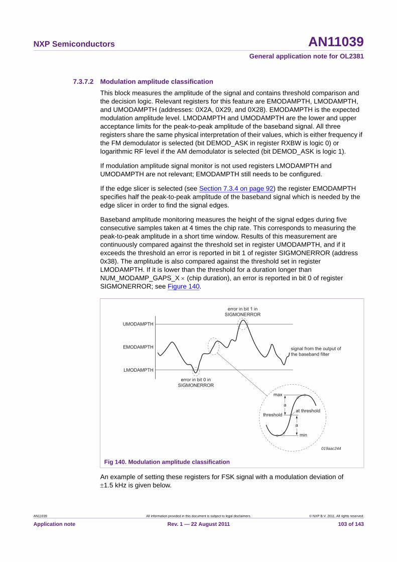
NXP Semiconductors AN11039General application note for OL2381
7.3.7.2 Modulation amplitude classification
This block measures the amplitude of the signal and contains threshold comparison and the decision logic. Relevant registers for this feature are EMODAMPTH, LMODAMPTH, and UMODAMPTH (addresses: 0X2A, 0X29, and 0X28). EMODAMPTH is the expected modulation amplitude level. LMODAMPTH and UMODAMPTH are the lower and upper acceptance limits for the peak-to-peak amplitude of the baseband signal. All three registers share the same physical interpretation of their values, which is either frequency if the FM demodulator is selected (bit DEMOD_ASK in register RXBW is logic 0) or logarithmic RF level if the AM demodulator is selected (bit DEMOD_ASK is logic 1).
If modulation amplitude signal monitor is not used registers LMODAMPTH and UMODAMPTH are not relevant; EMODAMPTH still needs to be configured.
If the edge slicer is selected (see Section 7.3.4 on page 92) the register EMODAMPTH specifies half the peak-to-peak amplitude of the baseband signal which is needed by the edge slicer in order to find the signal edges.
Baseband amplitude monitoring measures the height of the signal edges during five consecutive samples taken at 4 times the chip rate. This corresponds to measuring the peak-to-peak amplitude in a short time window. Results of this measurement are continuously compared against the threshold set in register UMODAMPTH, and if it exceeds the threshold an error is reported in bit 1 of register SIGMONERROR (address 0x38). The amplitude is also compared against the threshold set in register LMODAMPTH. If it is lower than the threshold for a duration longer than NUM_MODAMP_GAPS_X (chip duration), an error is reported in bit 0 of register SIGMONERROR; see Figure 140.
An example of setting these registers for FSK signal with a modulation deviation of 1.5 kHz is given below.
Fig 140. Modulation amplitude classification
019aac244
UMODAMPTH
EMODAMPTH
LMODAMPTH
error in bit 1 inSIGMONERROR
error in bit 0 inSIGMONERROR
signal from the output ofthe baseband filter
max
a
threshold
min
a
at threshold
AN11039 All information provided in this document is subject to legal disclaimers. © NXP B.V. 2011. All rights reserved.
Application note Rev. 1 — 22 August 2011 103 of 143

NXP Semiconductors AN11039General application note for OL2381
The FSK signal needs to be mapped to the output range of the FSK demodulator (0 to 32256).This range equals a frequency deviation of 200 kHz (see Section 7.3.1 on page 89).
The threshold for edge recognition in the edge slicer is half the expected peak-to-peak modulation amplitude, which is simply the frequency deviation used by the transmitter (1.5 kHz). It can be calculated using Equation 32.
(32)
The register EMODAMPTH should be set to the closest possible value (15 24 = 240).
EMODAMPTH [3:0] = 15d = 1111b
EMODAMPTH [7:4] = 4d = 0100b
The lower and upper thresholds for the peak-to-peak amplitude of the baseband signal (FSK modulation) are simply transmitted peak-to-peak frequency deviation plus and minus a guard band tolerance (multiplied by a factor of 3 / 4 or 5 / 4) mapped to the output range of the FSK demodulator. They can be calculated from following equations:
(33)
(34)
Register UMODAMPTH should be set to a value higher than 605 (10 26 = 640).
UMODAMPTH [3:0] = 10d = 1010b mantissa
UMODAMPTH [7:4] = 6d = 0110b exponent
Register LMODAMPTH should be set to a value lower than 362 (11 25 = 352).
LMODAMPTH [3:0] = 11d = 1011b mantissa
LMODAMPTH [7:4] = 5d = 0101b exponent
Figure 141 shows registers UMODAMPTH, LMODAMPTH, and EMODAMPTH which are used for setting the desired modulation amplitude range.
Fig 141. Registers UMODAMPTH, LMODAMPTH, and EMODAMPTH
EMODAMPTH 1500 32256 200000 242= =
LMODAMPTH 300032256200000------------------ 3
4--- 362= =
UMODAMPTH 300032256200000------------------ 5
4--- 605= =
019aac245
AN11039 All information provided in this document is subject to legal disclaimers. © NXP B.V. 2011. All rights reserved.
Application note Rev. 1 — 22 August 2011 104 of 143

NXP Semiconductors AN11039General application note for OL2381
Figure 143, Figure 144, Figure 145, and Figure 146 show examples of how the modulation amplitude classification can be used in a real application.
The same example using an FSK signal with a modulation deviation of 1.5 kHz and edge slicer is used.
The input sequence is not Manchester coded and the longest sequence of consecutive “0s” is 3.
In Figure 143, registers UMODAMPTH, LMODAMPTH, and EMODAMPTH are set to calculated values 106d, 91d and 79d. Register RXDCON0 (address 0x2B) is set to 0x80h (bits NUM_MODAMP_GAPS_W are “10”, 2 gaps or 3 consecutive “0s” are allowed). Figure 142 shows register RXDCON settings. More details are given in the OL2381 data sheet.
The yellow line (at the top) shows transmitted data, the brown line is baseband signal, the red line indicates that the baseband amplitude is lower than the limit set by LMODAMPTH (digital debug vector 9, bit 1), and the green line indicates that the baseband amplitude is higher than the limit set by UMODAMPTH (digital debug vector 9, bit 3). Cursors are set to the preamble marker. In this case both indicators are low during data transmission.
In Figure 144, registers UMODAMPTH, LMODAMPTH, and EMODAMPTH are set to values 103d (lower than calculated), 91d and 79d.
The green line indicates that the baseband amplitude is greater than the limit set by UMODAMPTH.
Fig 142. Register RXDCON0
Fig 143. Modulation amplitude indicators set correctly
019aac246
019aac247
TX data
Baseline signal
Baseband signal / LMODAMPTH
Baseband signal / UMODAMPTH
AN11039 All information provided in this document is subject to legal disclaimers. © NXP B.V. 2011. All rights reserved.
Application note Rev. 1 — 22 August 2011 105 of 143

NXP Semiconductors AN11039General application note for OL2381
In Figure 145, registers UMODAMPTH, LMODAMPTH, and EMODAMPTH are set to the calculated values 106d, 91d and 79d. Register RXDCON0 is set to 0x40h (bits NUM_MODAMP_GAPS_W are “01”, only 2 consecutive “0s” are allowed).
The red line indicates that the baseband amplitude is lower than the limit set by LMODAMPTH for a period greater than NUM_MODAMP_GAPS_X (chip duration).
In Figure 146, registers UMODAMPTH, LMODAMPTH, and EMODAMPTH are set to values 106d, 95d and 79d. Register RXDCON0 is set to 0x80h (3 consecutive “0s” are allowed).
The red line indicates that the baseband amplitude is lower than the limit set by LMODAMPTH.
Fig 144. Modulation amplitude indicators (high limit not set correctly)
Fig 145. Modulation amplitude indicators (NUM_MODAMP_GAPS not set correctly)
019aac248
TX data
Baseline signal
Baseband signal / LMODAMPTH
Baseband signal / UMODAMPTH
019aac249
TX data
Baseline signal
Baseband signal / LMODAMPTH
Baseband signal / UMODAMPTH
AN11039 All information provided in this document is subject to legal disclaimers. © NXP B.V. 2011. All rights reserved.
Application note Rev. 1 — 22 August 2011 106 of 143

NXP Semiconductors AN11039General application note for OL2381
If the input sequence is Manchester encoded (has at least one transition between each two-chip interval) one gap has to be accepted and ignored.
7.3.7.3 Timing classification block
The purpose of this unit is to classify the time intervals between the transitions from the slicer and to determine whether the received signal is a Manchester encoded signal.
Manchester encoded signals have only two different time intervals between two transitions: one chip width or two chip widths used as the main classification criterion in this block.
The slicer output signal is process by chip timing verification, code checker and baud rate checker.
Chip timing verification
The single chip timing verification block is a powerful means to classify signals.
The received signal is oversampled giving a time measurement resolution better than 1 %. The time interval between each pair of transitions is measured and it is checked whether the measured width is smaller than 3.5 chip (chip timeout value). Widths greater than 3.5 chip width are always rejected. If the measured time interval is accepted then it is compared to 1.5 chip width and according to the result, the associated nominal width of 1 chip or 2 chip is used to compute the timing error. This error is then compared to a limit which can be chosen to be less than: 12.5 %, 18.75 %, 25 % and 37.5 % of nominal chip width according to the setting of bits SGLBITTMGERRTH in register TIMINGHCHK (address: 0x34); see Figure 147. The time interval is accepted if its absolute value is below the limit. More details and single-chip timing block state diagrams are given in the OL2381 data sheet.
Fig 146. Modulation amplitude indicators (low limit not set correctly)
019aac250
TX data
Baseline signal
Baseband signal / LMODAMPTH
Baseband signal / UMODAMPTH
AN11039 All information provided in this document is subject to legal disclaimers. © NXP B.V. 2011. All rights reserved.
Application note Rev. 1 — 22 August 2011 107 of 143

NXP Semiconductors AN11039General application note for OL2381
Registers SIGMONSTATUS and SIGMONERROR (see Figure 117 on page 87) can be monitored while evaluating the following examples. Since data reception is used, register SIGMON2 (address: 0x30) shown in Figure 148 can be used to set and evaluate the signal monitor’s behavior.
The vector signal generator is used in the setup for the following examples. It is set to 434 MHz (the OL2381 operating frequency), data rate 2.6 kbit/s, sent data is Manchester encoded, frequency deviation 3 kHz, and output power 80 dBm. The output of the vector signal generator is connected to the OL2381 RFin connector.
The OL2381 is set to data reception mode at 2.4 kbit/s baud rate (registers TIMING0 and TIMING1). Register TIMINGCHK allows a single bit error of 37.5 % and a baud rate of 1.56 %.
Figure 149 shows an example of correct single bit timing and baud rate error. The yellow line (at the top) shows the transmitted data from the signal generator. The red, blue and green lines are respectively bits 6, 7, and 10 (baud rate valid, baud rate error, single bit error) signals from the digital debug interface, vector 9.
Fig 147. Register TIMINGCHK
Fig 148. Register SIGMON2
019aac251
019aac252
AN11039 All information provided in this document is subject to legal disclaimers. © NXP B.V. 2011. All rights reserved.
Application note Rev. 1 — 22 August 2011 108 of 143

NXP Semiconductors AN11039General application note for OL2381
Figure 150 shows an example of single bit timing error and baud rate error caused by single bit timing error.
The only change in the setup is in register TIMINGCHK, a single bit error of 12.5 % is allowed.
Baud rate checker
Since the single time interval check gives relatively rough limits for the baud rate of the received signal, an averaging is implemented to allow increasing the baud rate detection accuracy by a factor of 4. The averaging is performed on blocks of 8 bits.
Since averaging over 16 chips requires dividing the sum of the individual timing errors by 16, it would cause an unnecessary loss of precision, the division is skipped and the timing errors during an 8 bit block are summed. After 8 bits have been summed, the absolute value of the result is compared against a limit, which can be selected with bits SUMBITTMGERRTH (relative limit in % with respect to 8 nominal bits is between 0.78 and 9.38); see Figure 147 and the OL2381 data sheet. The baud rate is accepted, if the summed error is less than the selected threshold.
Fig 149. No single bit error, baud rate error example
Fig 150. Single bit error, baud rate error example
019aac253
TX data
Baud rate valid
Baud rate error
Single bit error
019aac254
TX data
Baud rate valid
Baud rate error
Single bit error
AN11039 All information provided in this document is subject to legal disclaimers. © NXP B.V. 2011. All rights reserved.
Application note Rev. 1 — 22 August 2011 109 of 143

NXP Semiconductors AN11039General application note for OL2381
This block can be easily extended to allow adjustment of the number of observed bits, which can be 8, 16, 24 or 32 bits according to the baud rate observation length setting BROBSLENGTH; see Figure 147 and the OL2381 data sheet.
The proper timing of a single bit is a prerequisite for the baud rate checker.
The baud rate checker has no information about the coding of the signal.
The typical application starts with WUPS and Manchester encoded data. More details about the baud checker block are given in the OL2381 data sheet.
Figure 151 shows an example of baud rate error.
The vector signal generator is set to 434 MHz (the OL2381 operating frequency), data rate 2.44 kbit/s, sent data are Manchester encoded, frequency deviation 3 kHz, and output power 80 dBm. The vector signal generator output is connected to the OL2381 RFin connector.
The OL2381 is set to data reception mode with 2.4 kbit/s baud rate (registers TIMING0 and TIMING1). Register TIMINGCHK allows a single bit error of 37.5 % (not important for this example) and a baud rate of 1.56 %.
Figure 152 shows an example of a valid baud rate result. The only difference from the previous setting is that a baud rate of 2.34 % is allowed in register TIMINGCHK.
Fig 151. Baud rate error example
019aac255
TX data
Baud rate valid
Baud rate error
Single bit error
AN11039 All information provided in this document is subject to legal disclaimers. © NXP B.V. 2011. All rights reserved.
Application note Rev. 1 — 22 August 2011 110 of 143
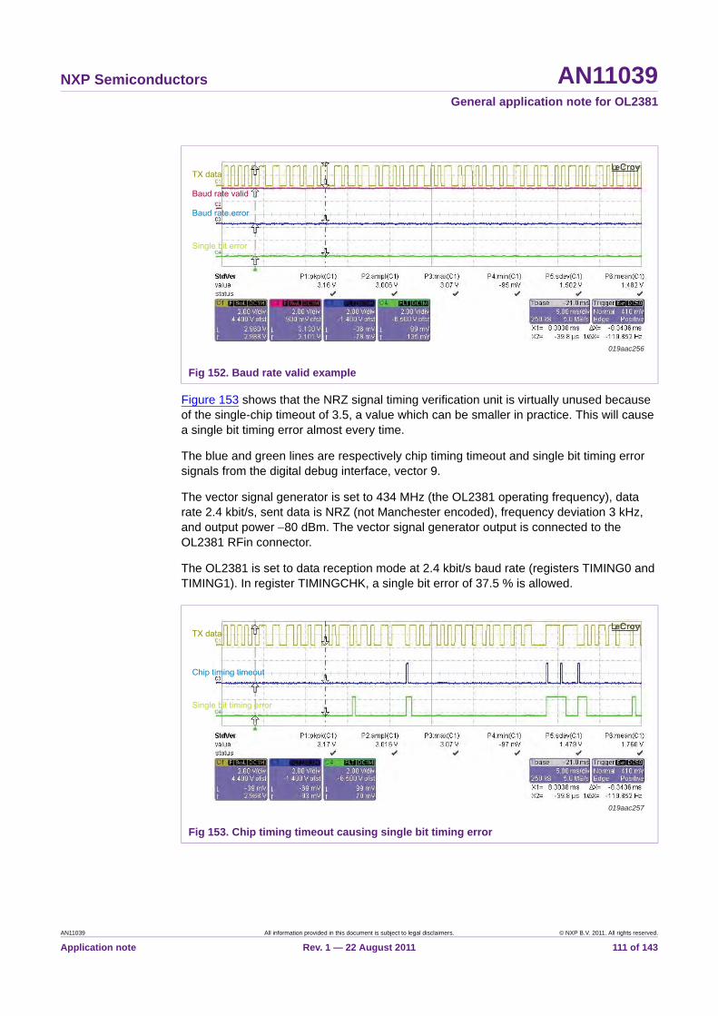
NXP Semiconductors AN11039General application note for OL2381
Figure 153 shows that the NRZ signal timing verification unit is virtually unused because of the single-chip timeout of 3.5, a value which can be smaller in practice. This will cause a single bit timing error almost every time.
The blue and green lines are respectively chip timing timeout and single bit timing error signals from the digital debug interface, vector 9.
The vector signal generator is set to 434 MHz (the OL2381 operating frequency), data rate 2.4 kbit/s, sent data is NRZ (not Manchester encoded), frequency deviation 3 kHz, and output power 80 dBm. The vector signal generator output is connected to the OL2381 RFin connector.
The OL2381 is set to data reception mode at 2.4 kbit/s baud rate (registers TIMING0 and TIMING1). In register TIMINGCHK, a single bit error of 37.5 % is allowed.
Fig 152. Baud rate valid example
Fig 153. Chip timing timeout causing single bit timing error
019aac256
TX data
Baud rate valid
Baud rate error
Single bit error
019aac257
TX data
Chip timing timeout
Single bit timing error
AN11039 All information provided in this document is subject to legal disclaimers. © NXP B.V. 2011. All rights reserved.
Application note Rev. 1 — 22 August 2011 111 of 143

NXP Semiconductors AN11039General application note for OL2381
Code checker
Typical wake-up patterns consist of either a constant 0 sequence, a constant 1 sequence or an alternating 01 sequence. In these cases, only one time interval is nominally contained in the wake-up pattern. Therefore, as an additional criteria during the WUPS four coding restriction, modes are available (no restriction, only short time interval accepted, only long time interval accepted, both are accepted and sequence is checked for Manchester encoding) as further restrictions on the accepted time intervals.
These criteria are chosen with bits CODING_RESTR_W in register RXDCON2 (address: 0x45); see Figure 125 on page 93 and the OL2381 data sheet. Since data reception is used for these examples, the relevant bit is CODING_RESTR_D. It can be set to logic 0 (accept 1 and 2 chips) and to logic 1 (accept 1 and 2 chips, Manchester encoded).
Correct chip timing is a prerequisite for the code checker. A single bit timing error consequently always causes a code checker error.
A typical application starts with WUPS and Manchester encoded data. More details and code checker block state diagrams are given in the OL2381 data sheet.
Figure 155 is an example showing single-chip timing error causing code checker error regardless of the setting.
The blue and green lines are respectively bits 9 and 10 (code checker error and single-bit timing error) signals from digital debug interface, vector 9.
The vector signal generator is set to 434 MHz (the OL2381 operating frequency), data rate 2.4 kbit/s, sent data Manchester encoded, frequency deviation 3 kHz, and output power 80 dBm. The vector signal generator output is connected to the OL2381 RFin connector.
The OL2381 is set to data reception mode at 2.4 kbit/s baud rate (registers TIMING0 and TIMING1). In register TIMINGCHK, a single bit error of 37.5 % is allowed. Bit CODING_RESTR_D in register RXDCON2 is set to logic 0 and later to logic 1.
Figure 154 shows a data sequence used for this example with three “1s” in a row which would cause a single-chip timing error and code check error.
Fig 154. Data sequence with three “1s” in a row
019aac258
AN11039 All information provided in this document is subject to legal disclaimers. © NXP B.V. 2011. All rights reserved.
Application note Rev. 1 — 22 August 2011 112 of 143

NXP Semiconductors AN11039General application note for OL2381
Figure 157 is an example showing an invalid Manchester sequence causing code checker error.
The blue and green lines are respectively bits 9 and 10 (code checker error and single-bit timing error) signals from the digital debug interface, vector 9.
The vector signal generator is set to 434 MHz (the OL2381 operating frequency), data rate 2.4 kbit/s, sent data Manchester encoded, frequency deviation 3 kHz, and output power 80 dBm. The vector signal generator output is connected to the OL2381 RFin connector.
The OL2381 is set to data reception mode at 2.4 kbit/s baud rate (registers TIMING0 and TIMING1). In register TIMINGCHK, a single bit error of 37.5 % is allowed. Bit CODING_RESTR_D in register RXDCON2 is set to logic 1 (both time intervals are accepted and sequence is checked for Manchester encoding).
Figure 156 shows a data sequence used for this example. This data sequence is not correct Manchester sequence (2 mistakes, “11” and later “00”) and there are no more than two “1s” or “0s” in a row. So single bit error is not there and code checker error is there when bit CODING_RESTR_D is logic 1.
Figure 157 has no code checker error but with the same conditions (data sequence and OL2381 settings). The only difference in settings is that this time, bit CODING_RESTR_D is set to logic 0 (no restrictions, both time intervals are accepted).
Fig 155. Single-chip timing error causing code check error
Fig 156. Invalid Manchester data sequence with two “1s” and two “0s” in a row
019aac259
Transmitted data
Code checker error
Single bit timing error
019aac260
AN11039 All information provided in this document is subject to legal disclaimers. © NXP B.V. 2011. All rights reserved.
Application note Rev. 1 — 22 August 2011 113 of 143

NXP Semiconductors AN11039General application note for OL2381
The same plot (Figure 159) can be observed if the correct Manchester data sequence is used (Figure 158). This is a correct Manchester data sequence, so both single bit error and code checker error are not there regardless of CODING_RESTR_D bit.
Fig 157. Code check error caused by invalid Manchester sequence
Fig 158. Valid Manchester data sequence
Fig 159. Code checker valid example
019aac261
Transmitted data
Code checker error
Single bit timing error
019aac285
019aac262
Transmitted data
Code checker error
Single bit timing error
AN11039 All information provided in this document is subject to legal disclaimers. © NXP B.V. 2011. All rights reserved.
Application note Rev. 1 — 22 August 2011 114 of 143

NXP Semiconductors AN11039General application note for OL2381
The wake-up search logic and timer are explained in more detail in the OL2381 data sheet. Section 7.1 on page 68 and Section 8.2 on page 125 of this application note also show some examples and block diagrams relevant to wake-up search.
7.4 BER measurement
The Bit Error Rate (BER) for given receiver parameters is the ultimate measure of receiver performance.
An external microcontroller is needed to send a test pattern to the OL2381, to compare this pattern with the output data processed by the OL2381 receiver, and to calculate the BER. Special software1 is needed to fulfill this. The source code and a compiled version are available in the software package.
The complete BER measurement setup is given in Figure 160. The digital multimeters do not necessary have to be used. They are used for current monitoring only.
Two OL2381 design-in-kits are used for this measurement. The BER measurement is only performed by the microcontroller in the OL2381 design-in-kit A. However, the OL2381 RF module needs to be attached due to the timing requirements.
The OL2381 design-in-kit B is set in continuous transparent data receive mode at 868 MHz using GUI software2. The configuration file for OL2381 B register settings is shown below:
//Start[LoPSTerRegisterConfiguration]FileFormat = V2.1NoOfConfigs = 1ActiveConfig = 1
1. Provided with the software package.
Fig 160. BER measurement setup
019aac263
600 Ω
1 kΩ
250 Ω
RF SIGNALGENERATOR
± 1 Vpp
ext. mod.
RFin OL2381DESIGN IN KIT
CONTROL + RF BOARD
POWER SUPPLY-11.7 V
VCC board
VCC board
P10 (OL2381)
RS232
II
PC COM3COM1
POWER SUPPLY
OL2381DESIGN-IN KIT A
CONTROL + RF BOARD
P12 (OL2381)RS232
P_RXA_LOP(μC)
μC
AN11039 All information provided in this document is subject to legal disclaimers. © NXP B.V. 2011. All rights reserved.
Application note Rev. 1 — 22 August 2011 115 of 143

NXP Semiconductors AN11039General application note for OL2381
[PresetConfig1]DeviceVersion = V0AConfigName = UpdateTime = 08/05/08 13:22:09; x0 x1 x2 x3 x4 x5 x6 x7 x8 x9 xA xB xC xD xE xF; visible in bank 0,101_0x = 00 00 B2 00 00 00 00 00 00 00 00 00 16 00 D5 5901_1x = 28 0E 60 08 00 81 FF 00 04 77 00 00 00 00 00 0001_2x = 00 F0 59 00 00 00 00 05 00 00 66 00 00 00 -- --01_3x = -- -- -- -- -- -- -- -- -- -- -- -- -- -- -- 01; visible in bank 00_2x = -- -- -- -- -- -- -- -- -- -- -- -- -- -- 00 000_3x = 00 00 00 00 4D 29 00 00 00 00 00 00 00 00 00 --; visible in bank 11_2x = -- -- -- -- -- -- -- -- -- -- -- -- -- -- 80 071_3x = 00 02 00 00 00 00 00 00 00 00 00 00 00 00 00 --TxRx = -- -- -- -- -- -- -- -- -- -- -- -- -- -- 80 80//Stop
The important registers for this measurement are shown in color (frequency and baud rate settings, channel filter bandwidth, LNA gain, baseband filter setting, expected deviation…). The remaining registers including PORTCON0 and PORTCON1 are mainly set to default values. TIMING0 and TIMING1 registers are set to 0xD5 and 0x59 which set the bit clock to 4.8 kHz and chip clock to 9.6 kHz. Finally, the receiver is activated by the receiver command.
The setup uses RF signal generator SMB100A R&S. In the following example it is set to 868 MHz (OL2381 operating frequency), FM modulation source external (Internal Mod. Gen. turned OFF), frequency deviation 4.8 kHz, low-noise mode, output power 60 dBm. The power supply of 11.7 V and additional resistors are used to provide 1V (p-p) voltage at the external modulation connector of the signal generator. The signal generator output is connected to the OL2381 B RFin connector.
The data flow starts at the microcontroller output P_RXA_LOP (design-in-kit A). The signal level is adjusted by a resistor divider to fit the modulation input of the RF generator. The FSK modulated carrier is connected to the OL2381 B RF input. The decoded transparent receive data is output at P10/DATA (OL2381 B) and fed back for comparison to the P12/(DATA_μC) input on the OL2381 design-in-kit A board. Microcontroller A calculates BER. The PC is used to control OL2381 design-in-kit B with GUI software via COM1 port and OL2381 design-in-kit B with BER software via COM3 port.
Checking the correct receiver configuration (OL2381 B) can be done in two steps:
1. The receive mode is activated with no RF input signal applied. Random noise should be seen as shown in Figure 161.
2. After applying a CW signal (no modulation) with a level of 60 dBm at the receiver input, the data output should change to a constant 1 or 0 as shown in Figure 162.
AN11039 All information provided in this document is subject to legal disclaimers. © NXP B.V. 2011. All rights reserved.
Application note Rev. 1 — 22 August 2011 116 of 143

NXP Semiconductors AN11039General application note for OL2381
A BER code for software P89LPC936 is available from NXP Semiconductors on request. The same setup and program can be used for BER measurement with different receiver parameters. The signal generator settings and configuration file of the OL2381 design-in-kit B should be changed accordingly.
There are two functions in the main BER program which could be run from the hyper terminal (PC):
MRXD - BER_EstimateRXDelay (wChipInterval)
This function measures the transmit-to-receive (round trip) delay between the MODULATOR_LINE and the RX_DATA_LINE.
128 delay measurements are performed and the measurements are averaged to give the final result. This function for each measurement produces 11 precisely evenly-spaced edges at the specified chip interval. After the last edge this function waits until the RX_DATA_LINE stabilizes at the final level and remains stable for at least 2 chip intervals. The measured delay is the time between the last transmitted edge and the last received edge before stabilizing.
Fig 161. Received data when no RF signal applied
Fig 162. Received data when CW signal applied
019aac264
019aac265
AN11039 All information provided in this document is subject to legal disclaimers. © NXP B.V. 2011. All rights reserved.
Application note Rev. 1 — 22 August 2011 117 of 143

NXP Semiconductors AN11039General application note for OL2381
Remark: The signal-to-noise ratio SNR during this measurement must be large enough to obtain error-free received data.
Figure 163 shows the correct data patterns which are sent (upper line, P_RXA_LOP) and received (lower line, P12/CLOCK) by the OL2381 microcontroller 1.
This function detects two error conditions:
• When the received signal stabilizes at the wrong logic level (timeout)
• When the difference between the maximum delay and the minimum delay is larger than half the chip interval: jitter too large increases SNR. The input chip interval is the nominal chip interval and the return value is the measured round trip delay. The unit of both is the number of PCLK periods.
If an error is detected, the transmitted data stops after five packets as shown in Figure 164 where no received signal appears on the microcontroller.
Fig 163. EstimateRXDelay function - correct
Fig 164. EstimateRXDelay function - error
019aac266
019aac267
AN11039 All information provided in this document is subject to legal disclaimers. © NXP B.V. 2011. All rights reserved.
Application note Rev. 1 — 22 August 2011 118 of 143

NXP Semiconductors AN11039General application note for OL2381
The OL2381 #1 sends and receives the known message and calculates the time delay between them. The argument is 3686500 / chip rate. 3686500 is half the microcontroller internal clock oscillator frequency and in our example the chip rate is 9600. MRXD (384) returns a chip delay of 787.
MCET - BER_MeasureNChipErrorsTransparent (wNchips, wChipInterval, wSamplingDelay, bit qManchester) – measures BER. The arguments are: scaled bit rate, numbers of bits to be sent, chip delay, and Manchester (1) or NRZ (0). The function returns numbers of errors.
In our example MCET (384, 10000, 787, 0) is run from the hyper terminal. 10000 bits are sent and when 10 bits with errors are received with errors this gives a sensitivity at the input for BER 103.
The input level to the OL2381 B should be adjusted to reach the specified BER. For each input level function, MCET should be started until the specified BER is reached. This input level, adjusted for cable losses, is the sensitivity of the receiver for the given parameters. In our example 110 dBm should be a typical value for receiver sensitivity.
Figure 165 shows data which is sent (upper line, P_RXA_LOP) and received (lower line, P12/CLOCK) by the OL2381 A microcontroller.
Figure 166 shows the hyper terminal display.
Fig 165. BER_MeasureNChipErrorsTransparent function
019aac268
AN11039 All information provided in this document is subject to legal disclaimers. © NXP B.V. 2011. All rights reserved.
Application note Rev. 1 — 22 August 2011 119 of 143

NXP Semiconductors AN11039General application note for OL2381
8. Application examples
8.1 Preamble detection
The OL2381 has an on-board signal signature recognition unit with preamble pattern recognition.
The value of the preamble is known in advance, so the value of the preamble in the receiver is configured according to this value.
Registers POLLACTION (or Receive command) and RXFOLLOWUP need to be properly configured as explained in Section 7.1.2 on page 70 in order to correctly use the preamble detection.
Section 8.1.2 presents the configuration of the preamble when NRZ or Manchester encoding are used.
8.1.1 Preamble configuration
The preamble consists of a configurable 1-to-32 bit pattern that can be implemented to aid power saving and avoid unintended wake-up due to ambient noise. It can be issued upon completion of a wake-up search or at any time when expecting a frame.
The preamble is configured in 5 registers. Register PREACON (address: 0x3A) configures the length of the preamble and the number of chip errors allowed during the preamble detection. Registers PREA0-PREA3 (addresses: 0x3B to 0x3E) provide the value of the preamble that should be recognized by the receiver.
The OL2381 receiver must know exactly the preamble sent by the transmitter. The transmit preamble is sent by the microcontroller. The length and the pattern are known by the receiver.
Fig 166. Hyper terminal display (results of the measurement)
019aac286
AN11039 All information provided in this document is subject to legal disclaimers. © NXP B.V. 2011. All rights reserved.
Application note Rev. 1 — 22 August 2011 120 of 143

NXP Semiconductors AN11039General application note for OL2381
8.1.2 Preamble examples (NRZ and Manchester)
In the following example for NRZ, coded preamble 0x14C is used as the preamble value. It is one of the recommended preambles to be used by the OL2381. Its length is 10 bits. The receiver is configured according to Figure 167.
In this example, registers PREA2 and PRE3 are not configured because they are not relevant for the application due to the shorter preamble.
The transmit clock must be configured for NRZ encoding as a bit clock. Bit TXCLKSEL of register TXCON (Figure 40 on page 38) is set to logic 0.
Figure 168 shows data communication, baud rate 20 kHz, with NRZ encoding.
Data is received (blue trace) only when the receiver recognizes a valid preamble pattern. Otherwise, the receiver enters predefine mode (stop or power-down).
The RX clock (green trace) is switched to the corresponding port pin (depending on the device configuration) after successful preamble detection. During preamble detection the clock pin is kept at a constant HIGH.
Fig 167. Register configurations for NRZ coded preamble 0x14C
Fig 168. NRZ data communication with preamble detection
019aac269
019aac270
Data Tx
0 0 0 0 0 011 1 1
Clock Tx
Data Rx
Clock Rx
AN11039 All information provided in this document is subject to legal disclaimers. © NXP B.V. 2011. All rights reserved.
Application note Rev. 1 — 22 August 2011 121 of 143

NXP Semiconductors AN11039General application note for OL2381
Applications using Manchester encoding have a different preamble configuration. The microcontroller sends the same preamble pattern: 0x14C. Since Manchester coding is used, the preamble pattern is coded with the data internally in the OL2381 transmitter.
The Manchester encoded 0x14C preamble is equal to 0x665A5 and in this case the preamble has a length of 20 bits.
The receiver is configured as shown in Figure 169.
The transmit clock needs to be configured for Manchester encoding as a chip clock. Bit TXCLKSEL of register TXCON (Figure 40 on page 38) is set to logic 1.
Figure 170 shows data communication, baud rate 20 kHz with Manchester encoding.
Data Tx and Clock Tx are the signals sent by the microcontroller to the OL2381 A (encoding is implemented inside the OL2381 later). Data is received only when the receiver recognizes the preamble pattern as valid. Otherwise, the receiver goes to the predefine mode (stop or power-down). Clock Rx is switched to the corresponding port pin, depending on the device configuration, after successful preamble detection. During preamble detection the clock pin is kept at a constant HIGH.
Fig 169. Register configurations for Manchester encoded preamble 0x14C
019aac271
AN11039 All information provided in this document is subject to legal disclaimers. © NXP B.V. 2011. All rights reserved.
Application note Rev. 1 — 22 August 2011 122 of 143

NXP Semiconductors AN11039General application note for OL2381
Figure 171 shows what is happening inside the OL2381 receiver in this case. Traces 1, 2, 7 and 8 correspond to those shown in Figure 170. Traces 3, 4, 5 and 6 show transmitted signals “in the air” and internal receiver signals, and cannot be observed with an oscilloscope.
Fig 170. Manchester data communication with preamble detection
Fig 171. Internal details of the Manchester data communication with preamble detection
019aac272
Data Tx
0 0 0 0 0 011 1 1
Clock Tx
Data Rx
Clock Rx
019aac273
AN11039 All information provided in this document is subject to legal disclaimers. © NXP B.V. 2011. All rights reserved.
Application note Rev. 1 — 22 August 2011 123 of 143
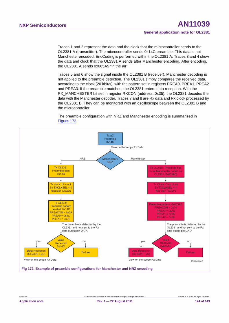
NXP Semiconductors AN11039General application note for OL2381
Traces 1 and 2 represent the data and the clock that the microcontroller sends to the OL2381 A (transmitter). The microcontroller sends 0x14C preamble. This data is not Manchester encoded. EncCoding is performed within the OL2381 A. Traces 3 and 4 show the data and clock that the OL2381 A sends after Manchester encoding. After encoding, the OL2381 A sends 0x665A5 “in the air”.
Traces 5 and 6 show the signal inside the OL2381 B (receiver). Manchester decoding is not applied to the preamble detection. The OL2381 simply compares the received data, according to the clock (20 kbit/s), with the pattern set in registers PREA0, PREA1, PREA2 and PREA3. If the preamble matches, the OL2381 enters data reception. With the RX_MANCHESTER bit set in register RXCON (address: 0x35), the OL2381 decodes the data with the Manchester decoder. Traces 7 and 8 are Rx data and Rx clock processed by the OL2381 B. They can be monitored with an oscilloscope between the OL2381 B and the microcontroller.
The preamble configuration with NRZ and Manchester encoding is summarized in Figure 172.
Fig 172. Example of preamble configurations for Manchester and NRZ encoding
019aac274
yes
NRZ
no yes
The preamble is detected by theOL2381 and not sent to the Rxdata output pin DATA
The preamble is detected by theOL2381 and not sent to the Rxdata output pin DATA
no
Manchester
View on the scope Tx Data
View on the scope Rx Data View on the scope Rx Data
Tx OL2381Preamble sent
0x14C
Tx OL2381: Preamble hasto be Manchester coded by
OL2381 (0x665A5)
Tx Clock: Chip clockBit TXCLKSEL = 1Register TXCON
Preamble pattern: 0x665A5PREACON = 0x14
PREA0 = 0xA5PREA1 = 0x65PREA2 = 0x06
Manchester /NRZ
Tx μCPreamble
0x14C
Tx clock: bit clockBit TXCLKSEL = 0Register TXCON
Tx OL2381Preamble patternneeded: 0x14C
PREACON = 0x0APREA0 = 0x4CPREA1 = 0x01
ValueReceived
0x14C
ValueReceived0x665A5
Data Reception(OL2381 + μC) Failure Data Reception
(OL2381 + μC) Failure
AN11039 All information provided in this document is subject to legal disclaimers. © NXP B.V. 2011. All rights reserved.
Application note Rev. 1 — 22 August 2011 124 of 143

NXP Semiconductors AN11039General application note for OL2381
8.2 Automatic reception
This section gives an example of the WUPS receive command initiated by the polling timer event.
After determining the optimum device configuration, the automatic operation sequences is used. Setting power-down bit (PD) to logic 1 in the PWRMODE register brings the device into the low current consumption standby mode. All analog receive and transmit circuits including the crystal oscillator are turned off and all dynamic digital activity is stopped. Only the SPI and the polling timer (if enabled by bit POLLTIM_EN) are active. The Receive command is automatically initiated as configured by registers POLLACTION and RXFOLLOWUP.
Successful WUPS is followed by preamble detection and data is received if the preamble detection is successful. The microcontroller takes action only after successful WUPS and preamble detection. Everything is performed automatically by the OL2381 when the registers are properly configured.
Setting POLLACTION to 0xC7 (see Figure 87 on page 71) configures the OL2381 to receive data on frequency channel 0 with the high gain settings and WUPS detection. Setting POLL_MODE to 11 brings the device to full power receive mode.
A polling time of 21 ms is chosen in the application and POLLWUPTIME (see Figure 88 on page 71) is set to 0x14.
Register RXFOLLOWUP (see Figure 90 on page 72) is configured for preamble detection after a successful WUPS. By setting it to 0xA8, the OL2381 enters power-down if the WUPS and/or preamble detection fail.
In this example, the OL2381 generates an interrupt, only after successful preamble detection, to wake up the microcontroller only after a successful WUPS and preamble detection.
The following procedure must be implemented in order to configure the OL2381 for automatic reception:
1. The registers presented above and the general registers (for example the frequency settings and baud rate) have to be properly configured.
2. The OL2381 is forced to power-down with the polling timer enabled by writing 0x12 to register PWRMODE.
3. The interrupt line is cleared (returned to the original state). Reading the register IFLAG clears P11 line.
Figure 173 shows an oscilloscope display of a communication between two OL2381s when the reception is implemented automatically. The yellow trace shows data (P10 or SDIO) sent by the OL2381 transmitter, the red trace shows data (P10 or SDIO) received by the OL2381 receiver, and the blue trace shows the interrupt line (P11) of the OL2381 receiver if the P11 is configured for interrupt request (D7 to D4 are 0010 in register PORTCON0).
AN11039 All information provided in this document is subject to legal disclaimers. © NXP B.V. 2011. All rights reserved.
Application note Rev. 1 — 22 August 2011 125 of 143

NXP Semiconductors AN11039General application note for OL2381
9. OL2381 conducted and radiated spurs and FCC/ETSI limits
International regulations regulate the use of radio receivers and transmitters. This section gives a summary of the most important regulations for license-free operation radio transceivers, for operating below 1 GHz.
Although the operation of transceivers in certain frequency bands is license free, the product itself has to be approved and meet certain requirements.
The scope of this section is to summarize FCC and ETSI requirements for spurious emissions and to present OL2381 results.
The spurious emission is a measurement of unwanted emitted signals. The device shall be measured without modulation applied. Measurements below 1 GHz shall be done with a quasi-peak detector, and a peak detector should be used above 1 GHz. If using a spectrum analyzer, the bandwidth must be 100 kHz.
9.1 European Union (EU) regulations
The use of radio equipment in the European Union (EU) is regulated by the R&TTE directive which sets the basic requirements. The actual standards are written by standardization bodies such as the ETSI. Section EN300220 is used for ETSI regulations in this section. Different EU countries can have different requirements. The local governing body should always be contacted before development starts to have a clear picture of the local rules.
Detailed information can be found in:
http://webapp.etsi.org/action/PE/PE20080829/en_30022001v020201c.pdf.
Maximum radiated effective field strength allowed for ETSI regulations is 110 dBV/m @ 3 m.
Fig 173. Automatic data reception
019aac275
P10/SDIO (Tx)
preamble
P10/SDIO (Rx)
P11 (Rx) Interrupt forsuccessful PRDA
AN11039 All information provided in this document is subject to legal disclaimers. © NXP B.V. 2011. All rights reserved.
Application note Rev. 1 — 22 August 2011 126 of 143

NXP Semiconductors AN11039General application note for OL2381
The limits for ETSI field strength of radiated spurs are: 59 dBV/m @ 3 m (up to 1 GHz) and 65 dBV/m @ 3 m (above 1 GHz). The spurs should be measured up to 4 GHz for an operating frequency up to 470 MHz and up to 12.75 GHz at higher operating frequencies.
The OL2381 operating frequency bands used in Europe and relevant for ETSI are 434 MHz and 868 MHz.
9.2 USA regulations
Federal Communications Commission (FCC) is responsible for the regulation of all RF devices in the United States. CFR 47, Part 15, regulates RF products intended for unlicensed operation. Section 15.231 is used for FCC regulations.
Detailed information can be found in:
http://www.fcc.gov/oet/info/rules/ :- Part15, PART15_07-10-08.pdf
FCC spurs should be measured up to the 10th harmonic.
The OL2381 operated frequency bands used in the USA and relevant for FCC are 315 MHz and 915 MHz. Bands 434 MHz and 868 MHz can also be used in the USA.
The maximum radiated effective field strength allowed for FCC regulations is: 75.6 dBV/m @ 3 m at 315 MHz (page 92) and 93.98 dBV/m @ 3 m at 915 MHz (page 106) and depends on the operating frequency.
The limit for radiated spurs for FCC is 20 dB lower than the transmitted carrier.
An advantage can be taken of the FCC rule to allow averaging. Actually, based on the modulation scheme, higher peak power can be transmitted while still maintaining the average limit. A correction factor (with appropriate protocol) of up to 20 dB can be used. The same correction factor can be used for spurious emissions. A maximum correction factor of 20 dB can be achieved with the FSK signal if the transmitter is ON for 10 ms in a 100 ms period and with ASK signal if the transmitter is ON for 20 ms in a 100 ms period.
This application note does not cover the rest of the world. The local governing body should always be contacted before development.
The following formulae can be used for converting different units:
(35)
(36)
(37)
9.3 Measurement results
The OL2381 reference board is designed by NXP Semiconductors to ensure that the OL2381 complies with the FCC/ETSI specifications for spurious emission. A complete reference design (all frequency bands) including schematic and layout files are available from NXP Semiconductors on request.
P[dBm] 10 log10P
1mW------------- =
P[dBW] 10 log10P
1W-------- =
FS V/m 10FS dBV/m /20
=
AN11039 All information provided in this document is subject to legal disclaimers. © NXP B.V. 2011. All rights reserved.
Application note Rev. 1 — 22 August 2011 127 of 143

NXP Semiconductors AN11039General application note for OL2381
The following results in this section are obtained with the OL2381 reference boards. Measurements are performed in the controlled environment in the NXP laboratory using a gigahertz transverse electromagnetic (GTEM) cell. It is a widely used alternative to open area test site (OATS) EMC testing.
The OL2381 reference board is placed inside the GTEM cell and its radiation is measured with a spectrum analyzer. The spectrum analyzer is software controlled. R&S software that includes the GTEM to OATS correlation is used.
The measurement results are presented as field strength in dBV/m @ 3 m unit so they can be easily compared with regulations.
The results of the OL2381 measurements at operating frequencies 315 MHz, 434 MHz, 868 MHz, and 902.8 MHz with PAM0 setting and maximum output power (ACON0 0x31) are shown in Figure 176, Figure 174, Figure 175, and Figure 177. FCC and ETSI limits for harmonics are shown in red.
These results show that the OL2381 reference board using the averaging rule for FCC is compliant with FCC/ETSI regulations in all bands.
The reason for the different ETSI limits for harmonics shown on the plots comes from the differences in the test setups. The maximum allowed averaging (20 dB) is used for FCC limits.
(1) Radiated harmonics.
(2) Harmonics limit.
Field strength measured at 3 m.
Fig 174. 434 MHz radiated harmonics with ETSI limit
f (GHz)0 141284 1062
019aac276
60
40
80
100field
strength(dBμV/m)
20
(1)
(2)
AN11039 All information provided in this document is subject to legal disclaimers. © NXP B.V. 2011. All rights reserved.
Application note Rev. 1 — 22 August 2011 128 of 143

NXP Semiconductors AN11039General application note for OL2381
(1) Radiated harmonics.
(2) Harmonics limit.
Field strength measured at 3 m.
Fig 175. 868 MHz radiated harmonics with ETSI limit
(1) Radiated harmonics.
(2) Harmonics limit; protocol allows minimum averaging in order to pass fundamental emission limit.
Field strength measured at 3 m.
Fig 176. 315 MHz radiated harmonics with FCC limit
f (GHz)0 141284 1062
019aac277
70
50
90
110field
strength(dBμV/m)
30
(1)
(2)
f (GHz)0 1084 62
019aac278
60
40
80
100field
strength(dBμV/m)
20
(1)
(2)
AN11039 All information provided in this document is subject to legal disclaimers. © NXP B.V. 2011. All rights reserved.
Application note Rev. 1 — 22 August 2011 129 of 143

NXP Semiconductors AN11039General application note for OL2381
Figure 178 shows conducted harmonics measured at an operating frequency of 434 MHz.
Figure 179 and Figure 180 show the schematic and response of the 434 MHz low-pass filter which is used after the power amplifier to reduce the level of harmonics.
Conducted emissions, low-pass filter schematics and simulation results for different frequencies are available.
(1) Radiated harmonics.
(2) Harmonics limit; protocol allows minimum averaging in order to pass fundamental emission limit.
Field strength measured at 3 m.
Fig 177. 902.8 MHz radiated harmonics with FCC limit
Fig 178. 434 MHz conducted harmonics
f (GHz)0 141284 1062
019aac279
70
50
90
110field
strength(dBμV/m)
30
(1)
(2)
019aac280
AN11039 All information provided in this document is subject to legal disclaimers. © NXP B.V. 2011. All rights reserved.
Application note Rev. 1 — 22 August 2011 130 of 143

NXP Semiconductors AN11039General application note for OL2381
10. OL2381 registers
A list of the OL2381 registers is shown in Table 30 according to their use: general, transmission, reception and test.
Fig 179. 434 MHz low-pass filter schematic
(1) f = 434.9 MHz; dB(S21) = 0.878.
(2) f = 866.6 MHz; dB(S21) = 21.563.
Fig 180. 434 MHz low-pass filter simulation results
019aac281
Term1Num = 1Z = 35 Ω
C1pn = GRM1555C1H50JZ01
L1
pn = LOG15HN12NJ02
C2pn = GRM1555C1H50JZ01
Term2Num = 2Z = 50 Ω
S-PARAMETERS
FINALSTART = 1 MHZSTOP = 4 GHZSTEP = 0.1 MHz
f (GHz)0 4321
019aac282
-60
-40
-80
-20
0
S21(dB)
-100
(1)
(2)
AN11039 All information provided in this document is subject to legal disclaimers. © NXP B.V. 2011. All rights reserved.
Application note Rev. 1 — 22 August 2011 131 of 143

xxxxxxxxxxxxxxxxxxxxx xxxxxxxxxxxxxxxxxxxxxxxxxx xxxxxxx x x x xxxxxxxxxxxxxxxxxxxxxxxxxxxxxx xxxxxxxxxxxxxxxxxxx xx xx xxxxx xxxxxxxxxxxxxxxxxxxxxxxxxxx xxxxxxxxxxxxxxxxxxx xxxxxx xxxxxxxxxxxxxxxxxxxxxxxxxxxxxxxxxxx xxxxxxxxxxxx x x xxxxxxxxxxxxxxxxxxxxx xxxxxxxxxxxxxxxxxxxxxxxxxxxxxx xxxxx xxxxxxxxxxxxxxxxxxxxxxxxxxxxxxxxxxxxxxxxxxxxxxxxxx xxxxxxxx xxxxxxxxxxxxxxxxxxxxxxxxx xxxxxxxxxxxxxxxxxxxx xxx
AN
11039
Ap
plicatio
n n
ote
NX
P S
emico
nd
ucto
rsA
N11039
Ge
nera
l ap
plic
ation
no
te fo
r OL
238
1
Table 30. Register map table
Register Addr Bank Bit Default value[7]
7 (MSB) 6 5 4 3 2 1 0 (LSB)
FC0L 00h 01 FC0L[1] 0 0 0 0 0000 0000
0000 0000
1011 0001
0 0 XXXX XXXX
XXXX XXXX
XXXX XXXX
0 0 XXXX XXXX
XXXX XXXX
XXXX XXXX
0 0 XXXX XXXX
XXXX XXXX
XXXX XXXX
0SXX XXXX
VCO_BAND[1]
RF_LO_DIV[1]
0000 0001
0000 0000
MAINSCH[1] 0110 0000[1] P10INV[1] 0010 1000
P12INV[1] 0000 1110[1] P14INV[1] 0000 0000
PD[3] RESET[3] 000S 0000
IE_BROWNOUT[1]
0 0000 0000
IF_BROWNOUT[1]
IF_POR[1] 0000 0001
1111 1111
IN[2] SET_RX_FLAGS[2]
00XX XXXX
EXT_CLK_BUF_EN[1]
XODIS[1] 0S00 0100
All inform
ation provided
in this docum
ent is subject to leg
al disclaim
ers.©
NX
P B
.V. 2011. A
ll rights reserved.
Rev. 1
— 22 A
ug
ust 2011
132 of 143
FC0M 01h 01 FC0M[1]
FC0H 02h 01 FC0H[1]
FC1L 03h 01 FC1L[2] 0 0
FC1M 04h 01 FC1M[2]
FC1H 05h 01 FC1H[2]
FC2L 06h 01 FC2L[2] 0 0
FC2M 07h 01 FC2M[2]
FC2H 08h 01 FC2H[2]
FC3L 09h 01 FC3L[2] 0 0
FC3M 0Ah 01 FC3M[2]
FC3H 0Bh 01 FC3H[2]
VCOCON 0Ch 01 FORCE_VCO_CAL[3]
VCO_CAL_RUNNING[4]
VCO_SUBBAND[2]
LOCON 0Dh 01 CLK2SCLK_DELAY[1] SKIP_VCOCAL[1]
LOCK_DETON[1]
TIMING0 0Eh 01 MAINSCL[1]
TIMING1 0Fh 01 WATCHDOG_TIME[1] PRESC[1]
PORTCON0 10h 01 P11C[1] P11INV[1] P10C
PORTCON1 11h 01 P13C[1] P13INV[1] P12C[1]
PORTCON2 12h 01 SEP_SDO[1] SEP_RX_OUT[1]
SEP_TX_LINES[1]
RFU[1] RFU[1] P14C
PWRMODE 13h 01 0 0 0 POLLTIM_EN[1]
DEV_MODE[5]
IEN 14h 01 IE_TXRX_RDY[1]
IE_EOF[1] IE_PREA[1] IE_WUPS[1] IE_POLLTIM[1]
IE_WATCHDOG[1]
IFLAG 15h 01 IF_TXRX_RDY[1]
IF_EOF[1] IF_PREA[1] IF_WUPS[1] IF_POLLTIM[1]
IF_WATCHDOG[1]
POLLWUPTIME 16h 01 POLLWUPTIME[1]
POLLACTION 17h 01 POLL_MODE[1] RX_FREQ[2] RX_CMD[2] RX_GA
CLOCKCON 18h 01 MANUALPTCAL[3]
PTCALRUNNING[4]
EXTPOLLTIMRNG[1]
CLKSOURCESEL[1]

xxxxxxxxxxxxxxxxxxxxx xxxxxxxxxxxxxxxxxxxxxxxxxx xxxxxxx x x x xxxxxxxxxxxxxxxxxxxxxxxxxxxxxx xxxxxxxxxxxxxxxxxxx xx xx xxxxx xxxxxxxxxxxxxxxxxxxxxxxxxxx xxxxxxxxxxxxxxxxxxx xxxxxx xxxxxxxxxxxxxxxxxxxxxxxxxxxxxxxxxxx xxxxxxxxxxxx x x xxxxxxxxxxxxxxxxxxxxx xxxxxxxxxxxxxxxxxxxxxxxxxxxxxx xxxxx xxxxxxxxxxxxxxxxxxxxxxxxxxxxxxxxxxxxxxxxxxxxxxxxxx xxxxxxxx xxxxxxxxxxxxxxxxxxxxxxxxx xxxxxxxxxxxxxxxxxxxx xxx
AN
11039
Ap
plicatio
n n
ote
NX
P S
emico
nd
ucto
rsA
N11039
Ge
nera
l ap
plic
ation
no
te fo
r OL
238
1DEVSTATUS 19h 01 0 PA_ON[4] PA_PWR_
RDY[4]LO-PWR_
RDY[4]RX_RDY[4] TX_RDY[4] LO_RDY[4] REFCLK_
RDY[4]0SSS SSSS
XXXX XXXX
ANT[2] 0XXX XXXX
10X1 1111
X00X XXXX
0000 0000
0XX0 0000
PAM RFU[1] 0000 0001
GAIN[1] 1111 0000
R_FC[2] X000 XXXX
0XXX XXXX
XXXX XXXX
XXXX XXXX
XXXX XXXX
ILTER_FC[2] XXXX XXXX
P_TH_MANT[2] XXXX XXXX
P_TH_MANT[2] XXXX XXXX
_TH_MANT[2] XXXX XXXX
INIT_ACQ_BITS_W[2] XXXX XXXX
INIT_ACQ_BITS_PD[2] XXXX XXXX
CODINGRESTR_P[2]
CODINGRESTR_D[2]
XXXX XXXX
0 XXXX XXX0
ACCU_SIGFAILS_P[2]
0XXX XXXX
Table 30. Register map table …continued
Register Addr Bank Bit Default value[7]
7 (MSB) 6 5 4 3 2 1 0 (LSB)
All inform
ation provided
in this docum
ent is subject to leg
al disclaim
ers.©
NX
P B
.V. 2011. A
ll rights reserved.
Rev. 1
— 22 A
ug
ust 2011
133 of 143
FDEV 1Ah 01 FDEV_EXP[2] FDEV_MANT[2]
FRMP 1Bh 01 0 FRMP_EXP[2] FRMP_M
ACON0 1Ch 01 ASK0[1] 0 AMH0X[2] AMH0[1]
ACON1 1Dh 01 ASK1[2] 0 0 AMH1[2]
ACON2 1Eh 01 0 0 0 AML[1]
ARMP 1Fh 01 0 ARMP_EXP[2] ARMP_MANT[1]
TXCON 20h 01 DOUBLE_SD_
RESULT[1]
INV_TX_DATA RFU[1]
TXCLKSEL RFU[1]
TXCLKOUTSEL RFU[1] RFU[1]
RXGAIN 21h 01 RX_HI_GAIN[1] RX_LOW_
RXBW 22h 01 DEMOD_ASK[2]
CF_BW[1] RSSI_FILTE
GAINSTEP 23h 01 0 RSSI_GAIN_STEP_ADJ[2]
HIGAINLIM 24h 01 HI_GAIN_LIMIT[2]
UPPERRSSITH 25h 01 UPPERRSSITH[2]
LOWERRSSITH 26h 01 LOWERRSSITH[2]
RXBBCON 27h 01 DEGLITCHER_WINDOW_LEN[2]
BASEBAND_SETTL_TIME[2]
BASEBAND_F
UMODAMPTH 28h 01 UPPER_MODAMP_TH_EXP[2] UPPER_MODAM
LMODAMPTH 29h 01 LOWER_MODAMP_TH_EXP[2] LOWER_MODAM
EMODAMPTH 2Ah 01 EDGE_MODAMP_TH_EXP[2] EDGE_MODAMP
RXDCON0 2Bh 01 NUM_MODAMP_GAPS_W[2]
SLICERSEL_W[2] SLICER_INITSEL_W[2]
RXDCON1 2Ch 01 NUM_MODAMP_GAPS_P[2]
SLICERSEL_P[2] SLICER_INITSEL_PD[2]
RXDCON2 2Dh 01 NUM_MODAMP_GAPS_D[2]
SLICERSEL_D[2] CODINGRESTR_W[2]
SIGMON0 2Eh 0 WUPS_MODE[2]
SIGMON_EN_W[2]
SIGMON1 2Fh 0 EN_PREADET_TIMEOUT[2]
SIGMON_EN_P[2]

xxxxxxxxxxxxxxxxxxxxx xxxxxxxxxxxxxxxxxxxxxxxxxx xxxxxxx x x x xxxxxxxxxxxxxxxxxxxxxxxxxxxxxx xxxxxxxxxxxxxxxxxxx xx xx xxxxx xxxxxxxxxxxxxxxxxxxxxxxxxxx xxxxxxxxxxxxxxxxxxx xxxxxx xxxxxxxxxxxxxxxxxxxxxxxxxxxxxxxxxxx xxxxxxxxxxxx x x xxxxxxxxxxxxxxxxxxxxx xxxxxxxxxxxxxxxxxxxxxxxxxxxxxx xxxxx xxxxxxxxxxxxxxxxxxxxxxxxxxxxxxxxxxxxxxxxxxxxxxxxxx xxxxxxxx xxxxxxxxxxxxxxxxxxxxxxxxx xxxxxxxxxxxxxxxxxxxx xxx
AN
11039
Ap
plicatio
n n
ote
NX
P S
emico
nd
ucto
rsA
N11039
Ge
nera
l ap
plic
ation
no
te fo
r OL
238
1SIGMON2 30h 0 0 SIGMON_EN_D[2] ACCU_SIG
FAILS_D[2]XXXX XXXX
XXXX XXXX
XXXX XXXX
0XXX XXXX
SGLBITTMGERRTH[2] XXXX XXXX
RX_CLOCKTRANSP[2]
RX_DATA_TRANSP[2]
XXXX XXXX
_CS[1] WUPS_FU_CF[1]
1000 1000
SSSS SSSS
SSSS SSSS
SSSS SSSS
XXXX XXXX
XXXX XXXX
XXXX XXXX
XXXX XXXX
XXXX XXXX
_COUNT[4] SSSS SSSS
L_RES[4] SS00 SSSS
0000 0000
0000 0100
LOCK_DET_TIME[1] 0100 1001
CAP_RSSI[1] 0000 0010
Table 30. Register map table …continued
Register Addr Bank Bit Default value[7]
7 (MSB) 6 5 4 3 2 1 0 (LSB)
All inform
ation provided
in this docum
ent is subject to leg
al disclaim
ers.©
NX
P B
.V. 2011. A
ll rights reserved.
Rev. 1
— 22 A
ug
ust 2011
134 of 143
WUPSTO 31h 0 WUPSTIMEOUTPRESC[2] WUPSTIMEOUT[2]
SLICERINITL 32h 0 SLICERINITTHR_LO[2]
SLICERINITH 33h 0 0 SLICERINITTHR_HI[2]
TIMINGCHK 34h 0 RFU[2] BROBSLENGTH[2] SUBMITTMGERRTH[2]
RXCON 35h 0 STATAUTOSAMPLE[2]
AUTOSAMPLE
MANUAL[2]
INV_RX_DATA[2]
CLOCK_RECOV_TC[2] RX_MANCHESTER[2]
RXFOLLOWUP 36h 0 PREA_FU_TF[1]
PREA_FU_CF[1]
WUPS_FU_TS[1] WUPS_FU_TF[1]
WUPS_FU
SIGMONSTATUS 37h 0 SIGMONSTATUS[4]
SIGMONERROR 38h 0 SIGMONERROR[4]
RSSILEVEL 39h 0 RSSI_LEVEL[4]
PREACON 3Ah 0 RFU[2] PREA_TOL[2] PREA_LEN[2]
PREA0 3Bh 0 PREA0[2]
PREA1 3Ch 0 PREA1[2]
PREA2 3Dh 0 PREA2[2]
PREA3 3Eh 0 PREA3[2]
EXTRXSTATUS 2Eh 1 RX_HI_GAIN[4]
LIVE_STATUS[4]
RXCMD[4] MANCHESTER
CFRCCAL 2Fh 1 CF_IQ_CAL_RUNNING
[4]
CF_RC_CAL_
RUNNING[4]
0 0 CF_RC_CA
CFIQCAL 30h 1 START_CF_IQ_CAL[3]
CF_IQ_CALVAL[1]
EXPERT0 31h 1 RED_VCO_SWING[1]
LARGE_PLL_RST_DELAY[1]
FASTCFFILTSETTL[1]
PLL_ICP[1]
EXPERT1 32h 1 XOSTARTUPDELAY[1] ASKRSTBBMID[1]
RFU[1] RFU[1] DISFRAC[1]
EXPERT2 33h 1 FM_DEM_IANDQ[1]
LARGE_FM_DEM_
RANGE[1]
WIDE_AMPL_
WINDOW[1]
REDUCED BIT_TIME[1]
TWORSSIMSBITS
SLOW[1]
FASTRSSIFILTSETTL
[1]

xxxxxxxxxxxxxxxxxxxxx xxxxxxxxxxxxxxxxxxxxxxxxxx xxxxxxx x x x xxxxxxxxxxxxxxxxxxxxxxxxxxxxxx xxxxxxxxxxxxxxxxxxx xx xx xxxxx xxxxxxxxxxxxxxxxxxxxxxxxxxx xxxxxxxxxxxxxxxxxxx xxxxxx xxxxxxxxxxxxxxxxxxxxxxxxxxxxxxxxxxx xxxxxxxxxxxx x x xxxxxxxxxxxxxxxxxxxxx xxxxxxxxxxxxxxxxxxxxxxxxxxxxxx xxxxx xxxxxxxxxxxxxxxxxxxxxxxxxxxxxxxxxxxxxxxxxxxxxxxxxx xxxxxxxx xxxxxxxxxxxxxxxxxxxxxxxxx xxxxxxxxxxxxxxxxxxxx xxx
AN
11039
Ap
plicatio
n n
ote
NX
P S
emico
nd
ucto
rsA
N11039
Ge
nera
l ap
plic
ation
no
te fo
r OL
238
1
vice status after a reset.
EXPERT3 34h 1 0 0 0 0 RFU[1] ALLOWREGSWITCH[6]
LTDIQPHASECAL
[1]
DONOTDISTURBPTCAP[1]
0000 0000
_SEL[6] 0110 0000
RL[6] VCO_TESTON[6]
0000 0000
FORCE_LOCK_
DETECTED[5]
FORCE_XO_RDY[1]
0000 0000
RX_ON[6] PA_STEP_TEST[6]
0000 0000
_CALVAL[2] 0000 XXXX
XO_DET_DIS[6]
XO_BIAS_DIS[6]
XXXX 0000
0000 0000
0000 0000
ASYNCSCAN[1]
SCANEN[1] 0000 0000
0000 0000
0 BANK_SEL[5]
0000 0000
Table 30. Register map table …continued
Register Addr Bank Bit Default value[7]
7 (MSB) 6 5 4 3 2 1 0 (LSB)
All inform
ation provided
in this docum
ent is subject to leg
al disclaim
ers.©
NX
P B
.V. 2011. A
ll rights reserved.
Rev. 1
— 22 A
ug
ust 2011
135 of 143
[1] Bits/field preset at power-on.
[2] Bits cannot be preset.
[3] Command bits.
[4] Status bit (Read only) and indicated by ‘S’ in the Default value column. Their values are undefined because they depend on the de
[5] Bits/field reset in power-down mode.
[6] Test bits.
[7] ‘X’ denotes the bit is undefined after a device reset; the value is completely random and independent of the device status.
TEST0 35h 1 CF_MULTITONE_EN[6]
DIG_TEST_SEL[6] RXD_DBG
TEST1 36h 1 IQ_TEST_LV[6]
ANA_TEST_SEL[6] REG_DIG_DIS[6]
PLL_CT
TEST2 37h 1 REG_VCO_ON[6]
REG_PLL_ON[6]
REG_PA_ON[6]
FORCE_REG_VCO_
RDY[5]
FORCE_REG_PLL_
RDY[5]
FORCE_REG_PA_
RDY[5]
TEST3 38h 1 VCO_ON[6] PRESC_ON[6]
PFD_ON[6] CLK_PLL_ON[6]
TX_ON[6] RX_GAP_ON[6]
TEST4 39h 1 FORCE_CF_RC_CAL[3]
SKIP_CF_RC_CAL[6]
CF_RC_ADJUSTCAL[6] MAN_CF_RC
TEST5 3Ah 1 XO_IOFFS[2] XO_IOFFSSINK_EN
[2]
XO_IOFFSEN[6]
XO_KICK_DIS[6]
RFU 3Bh 1 -[1]
TCBEN0 3Ch 1 -[3]
TCBR 3Dh 1 - IDDQ1[1] IDDQ0[1]
TCBEN1 3Eh 1 -[3]
BANKSEL 3Fh 01 0 0 0 0 0 0

NXP Semiconductors AN11039General application note for OL2381
11. Abbreviations
Table 31. Abbreviations
Acronym Description
AM Amplitude Modulation
ASK Amplitude-Shift Keying
ADC Analog-to-Digital Converter
BER Bit Error Rate
CW Continuous Wave
DAC Digital-to-Analog Converter
EOF End Of File
FM Frequency Modulation
FRMP FSK RaMP
FSK Frequency Shift Keying
GFSK Gaussian Frequency Shift Keying
ICP Input Compression Point
IF Intermediate Frequency
ISM Industrial, Scientific and Medical
LC inductor Capacitor
LNA Low-Noise Amplifier
LO Local Oscillator
LSB Least Significant Bit
MISO Master In Slave Out
MOSI Master Out Slave In
MSB Most Significant Bit
NRZ Not Return to Zero
OSR OverSampling Ratio
PA Power Amplifier
PAM Power Amplifier Mode
PFD Phase Frequency Detector
PLL Phase-Locked Loop
POR Power-On Reset
PRDA PReamble detection followed by DAta reception
PREA PREAmble
PRNG Pseudo-Random Number Generator
RC Resistor Capacitor
RF Radio Frequency
RFU Reserved for Future Use
RSSI Residual Signal Strength Indicator
RT Room Temperature
RX Receiver
SAW Surface Acoustic Wave
SFR Special Function Register
AN11039 All information provided in this document is subject to legal disclaimers. © NXP B.V. 2011. All rights reserved.
Application note Rev. 1 — 22 August 2011 136 of 143

NXP Semiconductors AN11039General application note for OL2381
12. References
[1] Raab F., Idealized operation of the class E tuned power amplifier: IEEE Transactions on circuits and systems; issue date: Dec 1977, volume: 24; issue: 12, pages: 725 to 735; ISSN: 0098-4094; digital object identifier: 10.1109/TCS.1977.1084296.
SPI Serial Peripheral Interface
SRD Short-Range Device
TX Transmitter
VCO Voltage-Controlled Oscillator
WUP Wake UP
WUPS Wake UP Search
XO Crystal Oscillator
Table 31. Abbreviations …continued
Acronym Description
AN11039 All information provided in this document is subject to legal disclaimers. © NXP B.V. 2011. All rights reserved.
Application note Rev. 1 — 22 August 2011 137 of 143

NXP Semiconductors AN11039General application note for OL2381
13. Legal information
13.1 Definitions
Draft — The document is a draft version only. The content is still under internal review and subject to formal approval, which may result in modifications or additions. NXP Semiconductors does not give any representations or warranties as to the accuracy or completeness of information included herein and shall have no liability for the consequences of use of such information.
13.2 Disclaimers
Limited warranty and liability — Information in this document is believed to be accurate and reliable. However, NXP Semiconductors does not give any representations or warranties, expressed or implied, as to the accuracy or completeness of such information and shall have no liability for the consequences of use of such information.
In no event shall NXP Semiconductors be liable for any indirect, incidental, punitive, special or consequential damages (including - without limitation - lost profits, lost savings, business interruption, costs related to the removal or replacement of any products or rework charges) whether or not such damages are based on tort (including negligence), warranty, breach of contract or any other legal theory.
Notwithstanding any damages that customer might incur for any reason whatsoever, NXP Semiconductors’ aggregate and cumulative liability towards customer for the products described herein shall be limited in accordance with the Terms and conditions of commercial sale of NXP Semiconductors.
Right to make changes — NXP Semiconductors reserves the right to make changes to information published in this document, including without limitation specifications and product descriptions, at any time and without notice. This document supersedes and replaces all information supplied prior to the publication hereof.
Suitability for use — NXP Semiconductors products are not designed, authorized or warranted to be suitable for use in life support, life-critical or safety-critical systems or equipment, nor in applications where failure or malfunction of an NXP Semiconductors product can reasonably be expected to result in personal injury, death or severe property or environmental damage. NXP Semiconductors accepts no liability for inclusion and/or use of NXP Semiconductors products in such equipment or applications and therefore such inclusion and/or use is at the customer’s own risk.
Applications — Applications that are described herein for any of these products are for illustrative purposes only. NXP Semiconductors makes no representation or warranty that such applications will be suitable for the specified use without further testing or modification.
Customers are responsible for the design and operation of their applications and products using NXP Semiconductors products, and NXP Semiconductors accepts no liability for any assistance with applications or customer product
design. It is customer’s sole responsibility to determine whether the NXP Semiconductors product is suitable and fit for the customer’s applications and products planned, as well as for the planned application and use of customer’s third party customer(s). Customers should provide appropriate design and operating safeguards to minimize the risks associated with their applications and products.
NXP Semiconductors does not accept any liability related to any default, damage, costs or problem which is based on any weakness or default in the customer’s applications or products, or the application or use by customer’s third party customer(s). Customer is responsible for doing all necessary testing for the customer’s applications and products using NXP Semiconductors products in order to avoid a default of the applications and the products or of the application or use by customer’s third party customer(s). NXP does not accept any liability in this respect.
Export control — This document as well as the item(s) described herein may be subject to export control regulations. Export might require a prior authorization from national authorities.
Evaluation products — This product is provided on an “as is” and “with all faults” basis for evaluation purposes only. NXP Semiconductors, its affiliates and their suppliers expressly disclaim all warranties, whether express, implied or statutory, including but not limited to the implied warranties of non-infringement, merchantability and fitness for a particular purpose. The entire risk as to the quality, or arising out of the use or performance, of this product remains with customer.
In no event shall NXP Semiconductors, its affiliates or their suppliers be liable to customer for any special, indirect, consequential, punitive or incidental damages (including without limitation damages for loss of business, business interruption, loss of use, loss of data or information, and the like) arising out the use of or inability to use the product, whether or not based on tort (including negligence), strict liability, breach of contract, breach of warranty or any other theory, even if advised of the possibility of such damages.
Notwithstanding any damages that customer might incur for any reason whatsoever (including without limitation, all damages referenced above and all direct or general damages), the entire liability of NXP Semiconductors, its affiliates and their suppliers and customer’s exclusive remedy for all of the foregoing shall be limited to actual damages incurred by customer based on reasonable reliance up to the greater of the amount actually paid by customer for the product or five dollars (US$5.00). The foregoing limitations, exclusions and disclaimers shall apply to the maximum extent permitted by applicable law, even if any remedy fails of its essential purpose.
13.3 TrademarksNotice: All referenced brands, product names, service names and trademarks are the property of their respective owners.
AN11039 All information provided in this document is subject to legal disclaimers. © NXP B.V. 2011. All rights reserved.
Application note Rev. 1 — 22 August 2011 138 of 143

NXP Semiconductors AN11039General application note for OL2381
14. Tables
Table 1. Component description. . . . . . . . . . . . . . . . . . . .5Table 2. Layout guidelines . . . . . . . . . . . . . . . . . . . . . . . .8Table 3. SPI commands . . . . . . . . . . . . . . . . . . . . . . . . .13Table 4. Port configuration . . . . . . . . . . . . . . . . . . . . . . .17Table 5. DEV_MODE[1:0] device mode control
functions . . . . . . . . . . . . . . . . . . . . . . . . . . . . .19Table 6. Frequency selection register bit settings . . . . .20Table 7. Frequency setting registers . . . . . . . . . . . . . . .20Table 8. Frequency selection registers bits setting for
different carrier frequencies . . . . . . . . . . . . . . .21Table 9. VCO and carrier output frequencies . . . . . . . . .22Table 10. FCmax = F0000h (limited by design) . . . . . . . .26Table 11. FCmax = 58000h (limited by VCO range) . . . .26Table 12. Different baud rate settings. . . . . . . . . . . . . . . .30Table 13. Interrupt WUPS/PREA . . . . . . . . . . . . . . . . . . .34Table 14. Interrupt polling timer . . . . . . . . . . . . . . . . . . . .34Table 15. Configuration of bits CLKSOURCESEL . . . . . .35Table 16. Transmit clock options . . . . . . . . . . . . . . . . . . .37Table 17. Frequency band selection (bits A, B) . . . . . . . .42Table 18. Power amplifier control and synchronization
(bits C, D) . . . . . . . . . . . . . . . . . . . . . . . . . . . . .43Table 19. Power amplifier control and synchronization
(bits C, E) . . . . . . . . . . . . . . . . . . . . . . . . . . . . .43Table 20. Amplitude selection (bit F) . . . . . . . . . . . . . . . .43Table 21. PAM definition. . . . . . . . . . . . . . . . . . . . . . . . . .60Table 22. Class E matching; component values and
results . . . . . . . . . . . . . . . . . . . . . . . . . . . . . . . .64Table 23. Bits E, F: gain step/switch selection bits. . . . . .68Table 24. Sub-command selection (bits C, D) . . . . . . . . .68Table 25. Gain switch selection (bits E, F) . . . . . . . . . . . .68Table 26. Receive matching; component values and
results . . . . . . . . . . . . . . . . . . . . . . . . . . . . . . . .77Table 27. Functionalities of bits ANA_TEST_SEL in
register TEST1 . . . . . . . . . . . . . . . . . . . . . . . . .77Table 28. Dynamic receiver configuration sets. . . . . . . . .87Table 29. Status information for signal monitors,
SIGMONSTATUS, SIGMONERROR . . . . . . .100Table 30. Register map table . . . . . . . . . . . . . . . . . . . . .131Table 31. Abbreviations . . . . . . . . . . . . . . . . . . . . . . . . .135
AN11039 All information provided in this document is subject to legal disclaimers. © NXP B.V. 2011. All rights reserved.
Application note Rev. 1 — 22 August 2011 139 of 143
continued >>

NXP Semiconductors AN11039General application note for OL2381
15. Figures
Fig 1. Reference design schematic . . . . . . . . . . . . . . . . .4Fig 2. Reference design layout . . . . . . . . . . . . . . . . . . . .7Fig 3. RF pin diode switch schematic . . . . . . . . . . . . . .10Fig 4. Transmit path schematic . . . . . . . . . . . . . . . . . . . 11Fig 5. Transmit path results . . . . . . . . . . . . . . . . . . . . . . 11Fig 6. SPI communication and separate TX/RX data,
clock port and interrupt pins. . . . . . . . . . . . . . . . .12Fig 7. SPI timing diagram . . . . . . . . . . . . . . . . . . . . . . .12Fig 8. Oscilloscope SPI signals . . . . . . . . . . . . . . . . . . .13Fig 9. Four SPI lines of a read command . . . . . . . . . . .14Fig 10. OL2381 configuration for SPI communication . . .14Fig 11. PORTCON2 register set for SPI data
communication. . . . . . . . . . . . . . . . . . . . . . . . . . .14Fig 12. Transmit data timing diagram
(SEP_TX_LINES = 0) . . . . . . . . . . . . . . . . . . . . .15Fig 13. Receive data timing diagram
(SEP_RX_LINES = 0) . . . . . . . . . . . . . . . . . . . . .15Fig 14. OL2381 Configuration for port communication . .16Fig 15. Serial test vector interface format . . . . . . . . . . . .16Fig 16. Transmit data timing diagram
(SEP_TX_LINES = 1) . . . . . . . . . . . . . . . . . . . . .17Fig 17. Receive data timing diagram
(SEP_RX_LINES = 1) . . . . . . . . . . . . . . . . . . . . .18Fig 18. PWRMODE register when PLL is activated. . . . .18Fig 19. Register EXPERT0 . . . . . . . . . . . . . . . . . . . . . . .19Fig 20. Register VCOCON. . . . . . . . . . . . . . . . . . . . . . . .21Fig 21. Phase noise at 434 MHz and different ICP
settings . . . . . . . . . . . . . . . . . . . . . . . . . . . . . . . .23Fig 22. Register EXPERT1 . . . . . . . . . . . . . . . . . . . . . . .23Fig 23. PLL locking time measurement on oscilloscope .24Fig 24. FC = B0000h, RF_LO_DIV = 0 . . . . . . . . . . . . . .25Fig 25. FC = B0050h, RF_LO_DIV = 0 . . . . . . . . . . . . . .25Fig 26. FC = B0300h, RF_LO_DIV = 0 . . . . . . . . . . . . . .26Fig 27. Inaccessible RF frequency at fREF = 16 MHz. . . .27Fig 28. General register configuration flow chart . . . . . . .27Fig 29. Frequency settings at 434 MHz . . . . . . . . . . . . . .29Fig 30. Configuration of register LOCON for 434 MHz . .29Fig 31. Configuration of 9.6 kbit/s baud rate . . . . . . . . . .30Fig 32. Registers IEN and IFLAG . . . . . . . . . . . . . . . . . .32Fig 33. Interrupt generation . . . . . . . . . . . . . . . . . . . . . . .33Fig 34. Behavior of interrupt line (P11) . . . . . . . . . . . . . .34Fig 35. Register CLOCKCON to configure external clock35Fig 36. Configuration of PORTCON0 and PORTCON1 for
external clock on P11 or P12 . . . . . . . . . . . . . . . .35Fig 37. Configuration of registers PORTCON1 and
CLOCKCON . . . . . . . . . . . . . . . . . . . . . . . . . . . .36Fig 38. Output chip clock and output bit clock for 9.6 kHz
baud rate . . . . . . . . . . . . . . . . . . . . . . . . . . . . . . .36
Fig 39. Registers PORTCON1 and TEST0 configured to provide a 1 MHz external clock . . . . . . . . . . . . . . 37
Fig 40. Register TXCON . . . . . . . . . . . . . . . . . . . . . . . . . 37Fig 41. TX clock generated on pin SCLK . . . . . . . . . . . . 38Fig 42. TX clock generated on pin P12/CLOCK . . . . . . . 38Fig 43. RX clock generated on pin SCLK . . . . . . . . . . . . 38Fig 44. Rx clock generated on pin P12/CLOCK . . . . . . . 39Fig 45. Three clock signals generated simultaneously by
OL2381 . . . . . . . . . . . . . . . . . . . . . . . . . . . . . . . . 39Fig 46. Transmitter block diagram. . . . . . . . . . . . . . . . . . 40Fig 47. Flow chart showing registers to be configured for
transmitting . . . . . . . . . . . . . . . . . . . . . . . . . . . . . 41Fig 48. Configuration of register ACON0 for full output
power . . . . . . . . . . . . . . . . . . . . . . . . . . . . . . . . . 41Fig 49. Reset state of registers FDEV and FRMP . . . . . 42Fig 50. TRANSMIT Command register . . . . . . . . . . . . . . 42Fig 51. CW transmit signal at 434 MHz. . . . . . . . . . . . . . 44Fig 52. DEVSTATUS register . . . . . . . . . . . . . . . . . . . . . 44Fig 53. Register FDEV set to a frequency deviation of
±15 kHz . . . . . . . . . . . . . . . . . . . . . . . . . . . . . . . . 45Fig 54. TX signal at 434 MHz without frequency
deviation . . . . . . . . . . . . . . . . . . . . . . . . . . . . . . . 46Fig 55. TX signal at 434 MHz with a frequency
deviation of ±15 kHz . . . . . . . . . . . . . . . . . . . . . . 47Fig 56. FSK modulated signal at 9.6 kbit/s data rate
and ±15 kHz frequency deviation . . . . . . . . . . . . 48Fig 57. FSK modulated signal at 9.6 kbit/s data rate
and ±15 kHz frequency deviation in time domain 48Fig 58. FSK modulated signal with a ±100 kHz
frequency deviation . . . . . . . . . . . . . . . . . . . . . . . 49Fig 59. FSK modulated signal with a ±100 kHz
frequency deviation in time domain. . . . . . . . . . . 50Fig 60. FSK modulated signals at data rates of
9.6 kbit/s and 4.8 kbit/s . . . . . . . . . . . . . . . . . . . . 50Fig 61. Time domain view of the FSK modulated signals
with data rates of 9.6 kbit/s and 4.8 kbit/s . . . . . . 51Fig 62. FSK modulated signals with a frequency
deviation of ±15 kHz and different frequency ramps for a data rate of 9.6 kbit/s . . . . . . . . . . . . 52
Fig 63. FSK modulated signals with a frequency deviationof ±15 kHz and different frequency ramps in time domain for a data rate of 9.6 kbit/s . . . . . . . . . . . 53
Fig 64. Power amplifier control . . . . . . . . . . . . . . . . . . . . 54Fig 65. Registers ACON0 and ACON1 set for ASK
modulation. . . . . . . . . . . . . . . . . . . . . . . . . . . . . . 54Fig 66. Maximum amplitude setting of register ACON0
and minimum amplitude setting of ACON2 . . . . . 55Fig 67. ASK modulation with a maximum high level and
AN11039 All information provided in this document is subject to legal disclaimers. © NXP B.V. 2011. All rights reserved.
Application note Rev. 1 — 22 August 2011 140 of 143
continued >>

NXP Semiconductors AN11039General application note for OL2381
a minimum low level. . . . . . . . . . . . . . . . . . . . . . .55Fig 68. ASK modulation with a maximum high level and
different low levels . . . . . . . . . . . . . . . . . . . . . . . .56Fig 69. ASK modulation with different high levels and a
low level of 0x02 . . . . . . . . . . . . . . . . . . . . . . . . .56Fig 70. ASK modulation with different baud rates . . . . . .57Fig 71. Register ARMP . . . . . . . . . . . . . . . . . . . . . . . . . .57Fig 72. Variation of the amplitude ramp in ASK
modulation . . . . . . . . . . . . . . . . . . . . . . . . . . . . . .58Fig 73. Topology of a switched power amplifier . . . . . . . .59Fig 74. Switched power amplifier waveforms. . . . . . . . . .60Fig 75. Output power as a function of bits AMH0 . . . . . .61Fig 76. Schematic of class E matching network . . . . . . .61Fig 77. Class E power amplifier matching – simplified. . .62Fig 78. Class E power amplifier matching – 434 MHz . . .62Fig 79. Measuring Cb_eff. . . . . . . . . . . . . . . . . . . . . . . . .63Fig 80. Verification of Ri . . . . . . . . . . . . . . . . . . . . . . . . . .63Fig 81. Final Class E power amplifier matching at
434 MHz . . . . . . . . . . . . . . . . . . . . . . . . . . . . . . .63Fig 82. Low-pass filter response . . . . . . . . . . . . . . . . . . .64Fig 83. Conducted harmonics for different frequencies . .65Fig 84. RX block diagram . . . . . . . . . . . . . . . . . . . . . . . .66Fig 85. Flow chart of the registers to be configured for
receive operation . . . . . . . . . . . . . . . . . . . . . . . . .67Fig 86. Receive command register . . . . . . . . . . . . . . . . .68Fig 87. Register POLLACTION . . . . . . . . . . . . . . . . . . . .70Fig 88. Register POLLWUPTIME. . . . . . . . . . . . . . . . . . .70Fig 89. Polling timer events . . . . . . . . . . . . . . . . . . . . . . .71Fig 90. Register RXFOLLOWUP . . . . . . . . . . . . . . . . . . .71Fig 91. Flowchart of the OL2381 receive action . . . . . . .72Fig 92. Representation of the polling timer period . . . . . .73Fig 93. Representation of the polling timer period
(single channel example) . . . . . . . . . . . . . . . . . . .74Fig 94. Representation of the polling timer period (two
channels example). . . . . . . . . . . . . . . . . . . . . . . .75Fig 95. Smith chart of the S11 receiver input into
matching network 434 MHz . . . . . . . . . . . . . . . . .76Fig 96. Receive matching components for 434 MHz . . . .77Fig 97. Register TEST1 . . . . . . . . . . . . . . . . . . . . . . . . . .77Fig 98. Register RXGAIN. . . . . . . . . . . . . . . . . . . . . . . . .78Fig 99. Register RXBW for configuring the channel
filter . . . . . . . . . . . . . . . . . . . . . . . . . . . . . . . . . . .78Fig 100. Channel filter output . . . . . . . . . . . . . . . . . . . . . .79Fig 101. Channel filter outputs I and Q . . . . . . . . . . . . . . .80Fig 102. Channel filter output with a 300 kHz channel
filter bandwidth. . . . . . . . . . . . . . . . . . . . . . . . . . .80Fig 103. Channel filter output with a 50 kHz channel filter
bandwidth. . . . . . . . . . . . . . . . . . . . . . . . . . . . . . .81Fig 104. Register CFRCAL . . . . . . . . . . . . . . . . . . . . . . . .81Fig 105. Register TEST4. . . . . . . . . . . . . . . . . . . . . . . . . .81Fig 106. Channel filter output when RC calibration is
omitted . . . . . . . . . . . . . . . . . . . . . . . . . . . . . . . . 82Fig 107. Register CFIQCAL . . . . . . . . . . . . . . . . . . . . . . . 82Fig 108. Limiter output for a CW signal at 434 MHz and
-90 dBm. . . . . . . . . . . . . . . . . . . . . . . . . . . . . . . . 83Fig 109. Limiter output for a CW signal at 434 MHz and
-90 dBm same title as Fig 108? . . . . . . . . . . . . . 83Fig 110. Register RSSILEVEL . . . . . . . . . . . . . . . . . . . . . 83Fig 111. Register RXCON. . . . . . . . . . . . . . . . . . . . . . . . . 84Fig 112. RSSI characteristic as a function of input power
level. . . . . . . . . . . . . . . . . . . . . . . . . . . . . . . . . . . 84Fig 113. Register GAINSTEP . . . . . . . . . . . . . . . . . . . . . . 84Fig 114. Register HIGAINLIM . . . . . . . . . . . . . . . . . . . . . . 85Fig 115. Register EXPERT2 . . . . . . . . . . . . . . . . . . . . . . . 85Fig 116. Registers UPPERRSSITH and LOWERRSSITH 86Fig 117. Signal monitoring configuration. . . . . . . . . . . . . . 86Fig 118. Receiver digital part block diagram . . . . . . . . . . . 87Fig 119. Register TEST0. . . . . . . . . . . . . . . . . . . . . . . . . . 88Fig 120. Digital test interface format . . . . . . . . . . . . . . . . . 89Fig 121. Baseband filter output (channel filter
comparison) . . . . . . . . . . . . . . . . . . . . . . . . . . . . 90Fig 122. RXBBCON register . . . . . . . . . . . . . . . . . . . . . . . 90Fig 123. Data sequence for test . . . . . . . . . . . . . . . . . . . . 91Fig 124. Baseband filter output (baseband filter
comparison) . . . . . . . . . . . . . . . . . . . . . . . . . . . . 91Fig 125. RXDCON1 and RXDCON2 registers . . . . . . . . . 92Fig 126. Control signals . . . . . . . . . . . . . . . . . . . . . . . . . . 93Fig 127. Modulated signal, channel filter and baseband
output observed on the oscilloscope. . . . . . . . . . 93Fig 128. Modulated signal in time domain at the
spectrum analyzer. . . . . . . . . . . . . . . . . . . . . . . . 94Fig 129. Baseband filter output, level slicer threshold and
level slicer output . . . . . . . . . . . . . . . . . . . . . . . . 94Fig 130. Baseband filter output, slicer threshold, and slicer
output for frequency offset signal . . . . . . . . . . . . 95Fig 131. Baseband filter output, slicer threshold, and slicer
output for long “1” sequence . . . . . . . . . . . . . . . . 95Fig 132. Baseband filter output and slicer threshold:
interferer with the same power present. . . . . . . . 96Fig 133. Baseband filter output and slicer output: interferer
with the same power present . . . . . . . . . . . . . . . 96Fig 134. Baseband filter output and slicer threshold:
interferer with 1 dB less power present. . . . . . . . 97Fig 135. Baseband filter output and slicer threshold:
interferer with 1 dB less power present same title as Fig 134? . . . . . . . . . . . . . . . . . . . . . . . . . . . . . 97
Fig 136. RSSI level for an input of -70 dBm, 104d . . . . . 100Fig 137. RSSI level indicators for an input of -20 dBm . . 101Fig 138. RSSI level indicators for an input of -70 dBm . . 101Fig 139. RSSI level indicators for an input of -100 dBm . 101Fig 140. Modulation amplitude classification . . . . . . . . . 102Fig 141. Registers UMODAMPTH, LMODAMPTH, and
AN11039 All information provided in this document is subject to legal disclaimers. © NXP B.V. 2011. All rights reserved.
Application note Rev. 1 — 22 August 2011 141 of 143
continued >>

NXP Semiconductors AN11039General application note for OL2381
EMODAMPTH . . . . . . . . . . . . . . . . . . . . . . . . . .103Fig 142. Register RXDCON0. . . . . . . . . . . . . . . . . . . . . .104Fig 143. Modulation amplitude indicators set correctly . .104Fig 144. Modulation amplitude indicators (high limit not
set correctly) . . . . . . . . . . . . . . . . . . . . . . . . . . .105Fig 145. Modulation amplitude indicators
(NUM_MODAMP_GAPS not set correctly) . . . .105Fig 146. Modulation amplitude indicators (low limit not
set correctly) . . . . . . . . . . . . . . . . . . . . . . . . . . .106Fig 147. Register TIMINGCHK . . . . . . . . . . . . . . . . . . . .107Fig 148. Register SIGMON2 . . . . . . . . . . . . . . . . . . . . . .107Fig 149. No single bit error, baud rate error example . . .108Fig 150. Single bit error, baud rate error example . . . . . .108Fig 151. Baud rate error example . . . . . . . . . . . . . . . . . .109Fig 152. Baud rate valid example . . . . . . . . . . . . . . . . . . 110Fig 153. Chip timing timeout causing single bit timing
error . . . . . . . . . . . . . . . . . . . . . . . . . . . . . . . . . . 110Fig 154. Data sequence with three “1s” in a row. . . . . . . 111Fig 155. Single-chip timing error causing code check
error . . . . . . . . . . . . . . . . . . . . . . . . . . . . . . . . . . 112Fig 156. Invalid Manchester data sequence with two “1s”
and two “0s” in a row . . . . . . . . . . . . . . . . . . . . . 112Fig 157. Code check error caused by invalid Manchester
sequence . . . . . . . . . . . . . . . . . . . . . . . . . . . . . . 113Fig 158. Valid Manchester data sequence . . . . . . . . . . . 113Fig 159. Code checker valid example . . . . . . . . . . . . . . . 113Fig 160. BER measurement setup . . . . . . . . . . . . . . . . . 114Fig 161. Received data when no RF signal applied . . . . 115Fig 162. Received data when CW signal applied . . . . . . 116Fig 163. OL2381 B configuration file . . . . . . . . . . . . . . . . 116Fig 164. EstimateRXDelay function - correct. . . . . . . . . . 117Fig 165. EstimateRXDelay function - error . . . . . . . . . . . 118Fig 166. BER_MeasureNChipErrorsTransparent
function . . . . . . . . . . . . . . . . . . . . . . . . . . . . . . . 119Fig 167. Hyper terminal display (results of the
measurement) . . . . . . . . . . . . . . . . . . . . . . . . . . 119Fig 168. Register configurations for NRZ coded
preamble 0x14C . . . . . . . . . . . . . . . . . . . . . . . .120Fig 169. NRZ data communication with preamble
detection . . . . . . . . . . . . . . . . . . . . . . . . . . . . . .121Fig 170. Register configurations for Manchester encoded
preamble 0x14C . . . . . . . . . . . . . . . . . . . . . . . .121Fig 171. Manchester data communication with preamble
detection . . . . . . . . . . . . . . . . . . . . . . . . . . . . . .122Fig 172. Internal details of the Manchester data
communication with preamble detection . . . . . .123Fig 173. Example of preamble configurations for
Manchester and NRZ encoding . . . . . . . . . . . . .124Fig 174. Automatic data reception. . . . . . . . . . . . . . . . . .125Fig 175. 434 MHz radiated harmonics with ETSI limit. . .128Fig 176. 868 MHz radiated harmonics with ETSI limit. . .128
Fig 177. 315 MHz radiated harmonics with FCC limit. . . 129Fig 178. 902.8 MHz radiated harmonics with FCC limit . 129Fig 179. 434 MHz conducted harmonics . . . . . . . . . . . . 130Fig 180. 434 MHz low-pass filter schematic . . . . . . . . . . 130Fig 181. 434 MHz low-pass filter simulation results . . . . 130
AN11039 All information provided in this document is subject to legal disclaimers. © NXP B.V. 2011. All rights reserved.
Application note Rev. 1 — 22 August 2011 142 of 143
continued >>

NXP Semiconductors AN11039General application note for OL2381
16. Contents
1 Introduction . . . . . . . . . . . . . . . . . . . . . . . . . . . . 3
2 Reference design. . . . . . . . . . . . . . . . . . . . . . . . 32.1 Schematic . . . . . . . . . . . . . . . . . . . . . . . . . . . . . 32.2 Layout. . . . . . . . . . . . . . . . . . . . . . . . . . . . . . . . 62.3 RF switch . . . . . . . . . . . . . . . . . . . . . . . . . . . . . 9
3 Interface description . . . . . . . . . . . . . . . . . . . . 113.1 SPI communication. . . . . . . . . . . . . . . . . . . . . 123.2 Port communication . . . . . . . . . . . . . . . . . . . . 16
4 Phase-locked loop . . . . . . . . . . . . . . . . . . . . . . 184.1 PLL operation . . . . . . . . . . . . . . . . . . . . . . . . . 194.2 Operating frequency . . . . . . . . . . . . . . . . . . . . 194.2.1 VCO auto calibration and sub-band selection 214.3 PLL measurement results. . . . . . . . . . . . . . . . 224.3.1 Phase noise measurements . . . . . . . . . . . . . . 224.3.2 PLL locking time . . . . . . . . . . . . . . . . . . . . . . . 234.3.3 Frequency range . . . . . . . . . . . . . . . . . . . . . . 244.3.3.1 Inappropriate FC settings . . . . . . . . . . . . . . . . 244.3.3.2 Extreme FC values . . . . . . . . . . . . . . . . . . . . . 264.3.3.3 Frequency range, fREF = 16 MHz . . . . . . . . . . 27
5 General register configuration . . . . . . . . . . . . 275.1 OL2381 reset . . . . . . . . . . . . . . . . . . . . . . . . . 285.2 Brown-out detection . . . . . . . . . . . . . . . . . . . . 285.3 Frequency and PLL settings. . . . . . . . . . . . . . 295.4 Baud rate configuration . . . . . . . . . . . . . . . . . 295.5 Watchdog timer. . . . . . . . . . . . . . . . . . . . . . . . 305.6 Interrupts. . . . . . . . . . . . . . . . . . . . . . . . . . . . . 315.7 Clock configuration . . . . . . . . . . . . . . . . . . . . . 345.7.1 External clock from register CLOCKCON. . . . 345.7.2 External 1 MHz clock . . . . . . . . . . . . . . . . . . . 375.7.3 TX clock . . . . . . . . . . . . . . . . . . . . . . . . . . . . . 375.7.4 RX clock . . . . . . . . . . . . . . . . . . . . . . . . . . . . . 385.7.5 Additional functions . . . . . . . . . . . . . . . . . . . . 39
6 Transmitter operation . . . . . . . . . . . . . . . . . . . 406.1 Introduction. . . . . . . . . . . . . . . . . . . . . . . . . . . 406.2 Power configuration . . . . . . . . . . . . . . . . . . . . 416.3 Transmit mode activation . . . . . . . . . . . . . . . . 426.4 FSK modulation . . . . . . . . . . . . . . . . . . . . . . . 446.4.1 Frequency deviation . . . . . . . . . . . . . . . . . . . . 456.4.2 Frequency modulation . . . . . . . . . . . . . . . . . . 476.4.3 Influence of frequency deviation and
modulation . . . . . . . . . . . . . . . . . . . . . . . . . . . 496.4.4 Soft FSK . . . . . . . . . . . . . . . . . . . . . . . . . . . . . 516.5 ASK modulation . . . . . . . . . . . . . . . . . . . . . . . 536.5.1 ASK modulation amplitude and baud rate . . . 536.5.2 Soft ASK . . . . . . . . . . . . . . . . . . . . . . . . . . . . . 576.6 Power amplifier . . . . . . . . . . . . . . . . . . . . . . . . 586.6.1 Power amplifier configuration . . . . . . . . . . . . . 60
6.6.2 Class E matching network . . . . . . . . . . . . . . . 61
7 Receiver operation . . . . . . . . . . . . . . . . . . . . . 657.1 Receive mode activation . . . . . . . . . . . . . . . . 677.1.1 Receive command . . . . . . . . . . . . . . . . . . . . . 677.1.2 Polling timer . . . . . . . . . . . . . . . . . . . . . . . . . . 697.1.2.1 OL2381 polling timer application examples . . 727.2 Receiver analog module . . . . . . . . . . . . . . . . 767.2.1 Receive matching . . . . . . . . . . . . . . . . . . . . . 767.2.2 Low-noise amplifier . . . . . . . . . . . . . . . . . . . . 787.2.3 Mixer . . . . . . . . . . . . . . . . . . . . . . . . . . . . . . . 787.2.4 Channel filter . . . . . . . . . . . . . . . . . . . . . . . . . 787.2.5 Limiter . . . . . . . . . . . . . . . . . . . . . . . . . . . . . . 827.2.6 RSSI. . . . . . . . . . . . . . . . . . . . . . . . . . . . . . . . 837.3 Receiver digital module . . . . . . . . . . . . . . . . . 867.3.1 Digital FM demodulator . . . . . . . . . . . . . . . . . 887.3.2 Digital test interface . . . . . . . . . . . . . . . . . . . . 887.3.3 Baseband filter . . . . . . . . . . . . . . . . . . . . . . . . 897.3.4 Data slicer . . . . . . . . . . . . . . . . . . . . . . . . . . . 917.3.4.1 Level-sensitive slicer . . . . . . . . . . . . . . . . . . . 927.3.5 De-glitcher . . . . . . . . . . . . . . . . . . . . . . . . . . . 977.3.6 Clock recovery for receive mode . . . . . . . . . . 987.3.7 Signal signature recognition unit . . . . . . . . . . 987.3.7.1 RSSI level classification. . . . . . . . . . . . . . . . 1007.3.7.2 Modulation amplitude classification . . . . . . . 1027.3.7.3 Timing classification block . . . . . . . . . . . . . . 1067.4 BER measurement. . . . . . . . . . . . . . . . . . . . . 114
8 Application examples . . . . . . . . . . . . . . . . . . . 1198.1 Preamble detection . . . . . . . . . . . . . . . . . . . . 1198.1.1 Preamble configuration . . . . . . . . . . . . . . . . 1208.1.2 Preamble examples (NRZ and Manchester) 1208.2 Automatic reception . . . . . . . . . . . . . . . . . . . 124
9 OL2381 conducted and radiated spurs and FCC/ETSI limits . . . . . . . . . . . . . . . . . . . . . . . 125
9.1 European Union (EU) regulations . . . . . . . . 1269.2 USA regulations . . . . . . . . . . . . . . . . . . . . . . 1269.3 Measurement results . . . . . . . . . . . . . . . . . . 127
10 OL2381 registers . . . . . . . . . . . . . . . . . . . . . . 130
11 Abbreviations . . . . . . . . . . . . . . . . . . . . . . . . 135
12 References. . . . . . . . . . . . . . . . . . . . . . . . . . . 136
13 Legal information . . . . . . . . . . . . . . . . . . . . . 13713.1 Definitions . . . . . . . . . . . . . . . . . . . . . . . . . . 13713.2 Disclaimers . . . . . . . . . . . . . . . . . . . . . . . . . 13713.3 Trademarks . . . . . . . . . . . . . . . . . . . . . . . . . 137
14 Tables . . . . . . . . . . . . . . . . . . . . . . . . . . . . . . . 138
15 Figures . . . . . . . . . . . . . . . . . . . . . . . . . . . . . . 139
16 Contents. . . . . . . . . . . . . . . . . . . . . . . . . . . . . 142
© NXP B.V. 2011. All rights reserved.
For more information, please visit: http://www.nxp.comFor sales office addresses, please send an email to: [email protected]
Date of release: 22 August 2011
Document identifier: AN11039
Please be aware that important notices concerning this document and the product(s)described herein, have been included in section ‘Legal information’.