Embed Size (px)
Citation preview
AN109231.5 GHz Doherty power amplifier for base station applications using the BLF6G15L-250PBRNRev. 2 — 1 September 2015 Application note
Document information
Info Content
Keywords RF power transistor, Doherty architecture, LDMOS, Power amplifier, W-CDMA, LTE, Base station, BLF6G15L-250PBRN
Abstract This application note describes the design and performance of a power amplifier for 1.5GHz 3GPP E-UTRA LTE base stations using two BLF6G15L-250PBRN LDMOS power transistors in Doherty architecture
AN109231.5 GHz Doherty power amplifier using the BLF6G15L-250PBRN
Revision history
Rev Date Description
AN10923#2 20150901 Modifications
• The format of this document has been redesigned to comply with the new identity guidelines of Ampleon.
• Legal texts have been adapted to the new company name where appropriate.
AN10923#1 20110314 Initial version
AN10923#2 All information provided in this document is subject to legal disclaimers. © Ampleon The Netherlands B.V. 2015. All rights reserved.
Application note Rev. 2 — 1 September 2015 2 of 20
Contact informationFor more information, please visit: http://www.ampleon.com
For sales office addresses, please visit: http://www.ampleon.com/sales
AN109231.5 GHz Doherty power amplifier using the BLF6G15L-250PBRN
1. Introduction
This application note describes the design and performance of a Doherty power amplifier optimized for use in 1.5 GHz 3GPP E-UTRA LTE base stations applications. The amplifier design, characteristics and the test methods used to determine the RF performance are also described.
The amplifier uses two BLF6G15L-250PBRN LDMOS power transistors in a Doherty architecture. The design ensures high efficiency while providing a peak power capability very similar to two parallel Class AB amplifiers. The input and output sections are internally matched, giving high gain with good gain flatness and phase linearity over a wide frequency band.
The BLF6G15L-250PBRN transistor is a sixth generation device using Ampleons’ advanced LDMOS process.
2. Circuit description
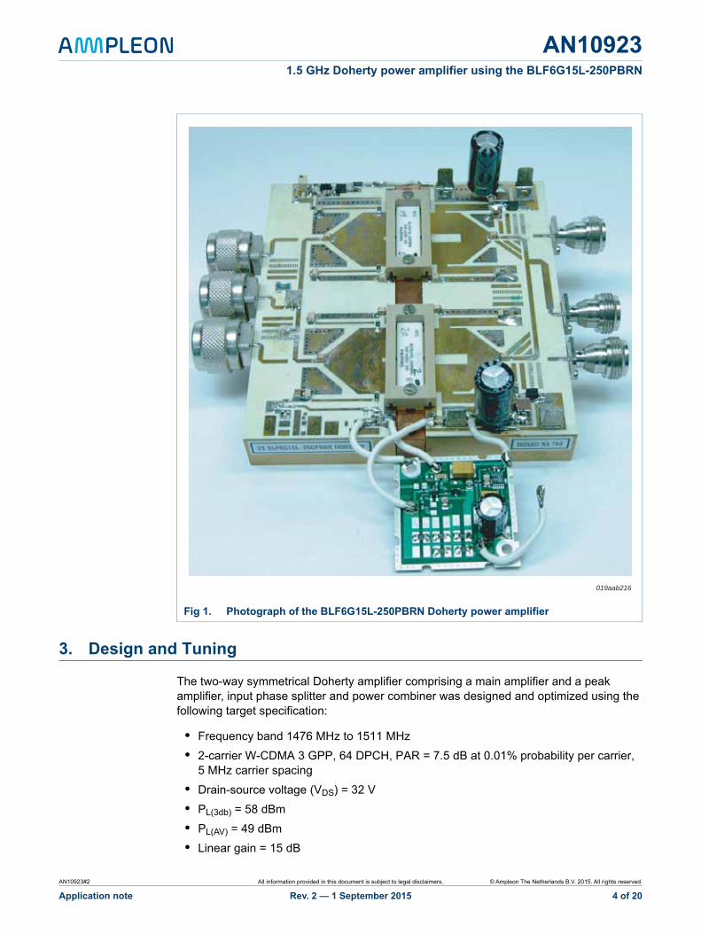
The 1.5 GHz Doherty power amplifier employing two BLF6G15L-250PBRN power transistors is shown in the photograph of Figure 1. The main amplifier is biased to operate in Class-AB mode and the peak amplifier is biased to operate in Class-C mode. The input signal is split by a 3 dB power divider and fed to each amplifier with a 90 degree phase difference. The amplified signals are recombined at the output with a power combiner. Both amplifiers operate when the input signal peaks, and each is presented with the load impedance that enables maximum output power. If the input signal amplitude drops below a preset threshold level, the Class-C peaking amplifier turns off and only the Class-AB remains active. At these lower power levels the Class-AB main amplifier is presented with higher load impedance that enables higher efficiency and gain. The result is an extremely efficient solution for amplifying the complex modulation schemes employed in current and emerging wireless systems.
AN10923#2 All information provided in this document is subject to legal disclaimers. © Ampleon The Netherlands B.V. 2015. All rights reserved.
Application note Rev. 2 — 1 September 2015 3 of 20
AN109231.5 GHz Doherty power amplifier using the BLF6G15L-250PBRN
3. Design and Tuning
The two-way symmetrical Doherty amplifier comprising a main amplifier and a peak amplifier, input phase splitter and power combiner was designed and optimized using the following target specification:
• Frequency band 1476 MHz to 1511 MHz
• 2-carrier W-CDMA 3 GPP, 64 DPCH, PAR = 7.5 dB at 0.01% probability per carrier, 5 MHz carrier spacing
• Drain-source voltage (VDS) = 32 V
• PL(3db) = 58 dBm
• PL(AV) = 49 dBm
• Linear gain = 15 dB
Fig 1. Photograph of the BLF6G15L-250PBRN Doherty power amplifier
019aab216
AN10923#2 All information provided in this document is subject to legal disclaimers. © Ampleon The Netherlands B.V. 2015. All rights reserved.
Application note Rev. 2 — 1 September 2015 4 of 20
AN109231.5 GHz Doherty power amplifier using the BLF6G15L-250PBRN
• Gain ripple 0.5 dB
• RLin 15 dB
• ACPR at 5 MHz offset and PL(AV) = 30 dBc
• Efficiency at PL(AV) = 36 %
• PCB material RO4350 30 mils
The description of the design of the single stage (Class-AB) amplifier is given in Section 3.1, and the description of the Doherty design is given in Section 3.2.
3.1 Design of the single stage amplifiers
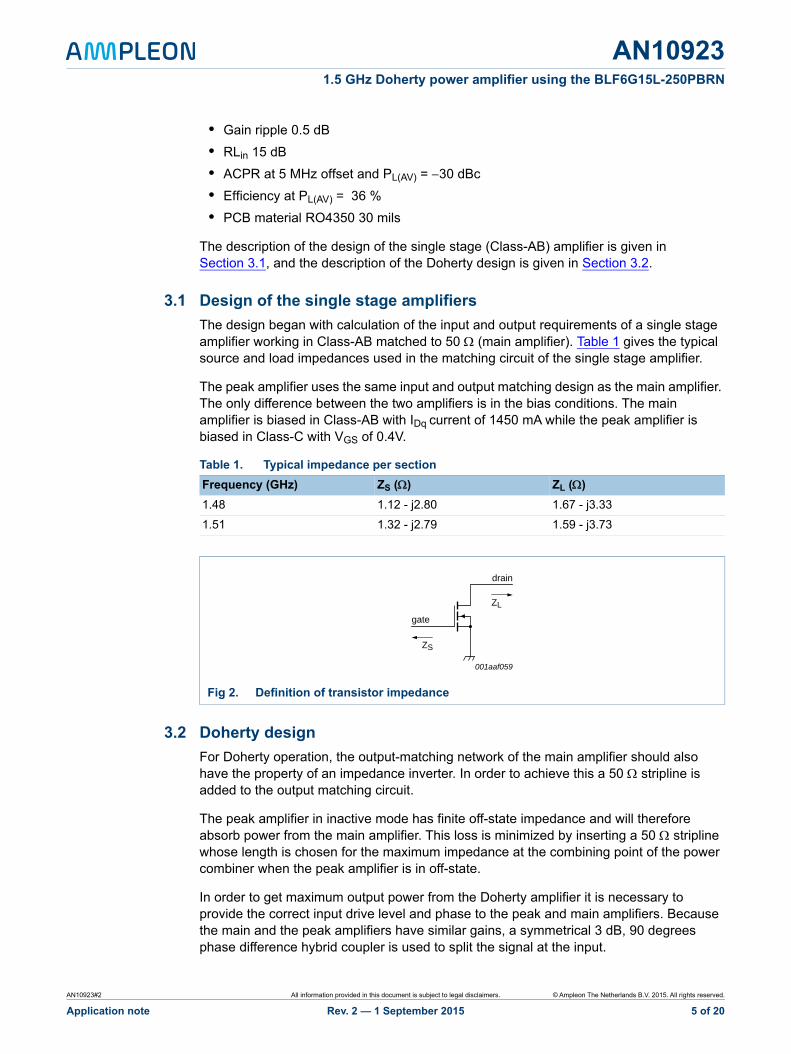
The design began with calculation of the input and output requirements of a single stage amplifier working in Class-AB matched to 50 (main amplifier). Table 1 gives the typical source and load impedances used in the matching circuit of the single stage amplifier.
The peak amplifier uses the same input and output matching design as the main amplifier. The only difference between the two amplifiers is in the bias conditions. The main amplifier is biased in Class-AB with IDq current of 1450 mA while the peak amplifier is biased in Class-C with VGS of 0.4V.
3.2 Doherty design
For Doherty operation, the output-matching network of the main amplifier should also have the property of an impedance inverter. In order to achieve this a 50 stripline is added to the output matching circuit.
The peak amplifier in inactive mode has finite off-state impedance and will therefore absorb power from the main amplifier. This loss is minimized by inserting a 50 stripline whose length is chosen for the maximum impedance at the combining point of the power combiner when the peak amplifier is in off-state.
In order to get maximum output power from the Doherty amplifier it is necessary to provide the correct input drive level and phase to the peak and main amplifiers. Because the main and the peak amplifiers have similar gains, a symmetrical 3 dB, 90 degrees phase difference hybrid coupler is used to split the signal at the input.
Table 1. Typical impedance per section
Frequency (GHz) ZS () ZL ()
1.48 1.12 - j2.80 1.67 - j3.33
1.51 1.32 - j2.79 1.59 - j3.73
Fig 2. Definition of transistor impedance
001aaf059
drain
ZL
ZS
gate
AN10923#2 All information provided in this document is subject to legal disclaimers. © Ampleon The Netherlands B.V. 2015. All rights reserved.
Application note Rev. 2 — 1 September 2015 5 of 20
AN109231.5 GHz Doherty power amplifier using the BLF6G15L-250PBRN
It is essential that the signals from the main and peak amplifiers arrive in phase at the combining point of the power combiner. The phase difference introduced by the length of impedance inverter stripline and the off-state maximum impedance stripline therefore needs to be compensated for at the input. The phase difference caused by the different classes of operation is very small and can be ignored.
The drain bias line is one of the strongest contributors to the memory effects by the amplifiers. Making the bias line as short as possible will have a positive effect on the memory performance. In order to further reduce the drain video impedance, two parallel bias lines are placed symmetrically on both sides of every transistor.
3.3 Tuning
Adjusting the bias of the peak amplifier can further optimize the back-off efficiency of the Doherty amplifier, however this will be at the cost of linearity. Another way to optimize linearity is by adjusting the input phase shift while monitoring the AM-AM and AM-PM characteristics. This however will be at the cost of peak power and peak efficiency.
3.4 Transistor biasing
There are two ways to bias the BLF6G15-250PBRN transistor. The first is standard bias without using the sense FETs integrated in the package. In this case the sense FET leads can be removed and the bias can be applied directly to the power transistor(s) (see Section 5 “Appendix A: PCB layout and bill of materials (no auto bias)”. The second way of biasing is by using the sense leads. An auto bias circuit is required to provide a fixed IDq to the main RF FET. The FET is biased by a sense transistor mounted in the same package which is used as a current mirror. Details of the circuit and layout are given in Section 6 “Appendix B: PCB layout and bill of materials with auto bias”, Figure 12 and Figure 13. The peak amplifier operates in Class-C and has a fixed gate-source voltage of 0.4 V.
4. Test results
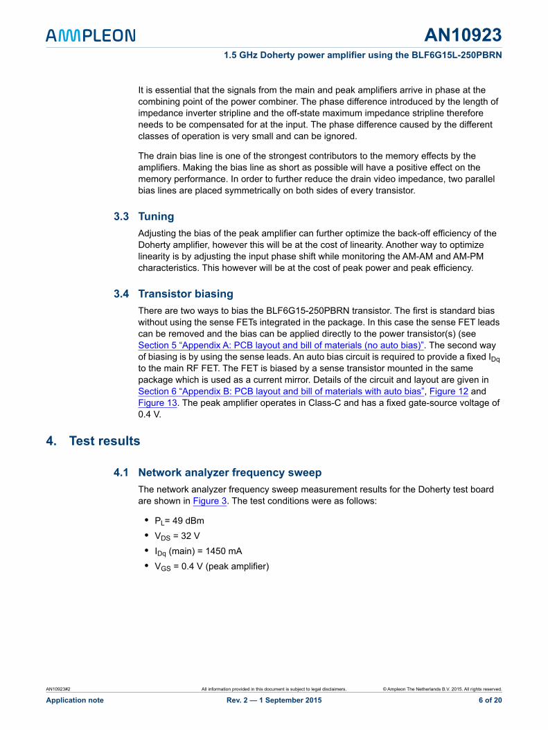
4.1 Network analyzer frequency sweep
The network analyzer frequency sweep measurement results for the Doherty test board are shown in Figure 3. The test conditions were as follows:
• PL= 49 dBm
• VDS = 32 V
• IDq (main) = 1450 mA
• VGS = 0.4 V (peak amplifier)
AN10923#2 All information provided in this document is subject to legal disclaimers. © Ampleon The Netherlands B.V. 2015. All rights reserved.
Application note Rev. 2 — 1 September 2015 6 of 20
AN109231.5 GHz Doherty power amplifier using the BLF6G15L-250PBRN
4.2 Large signal power sweeps
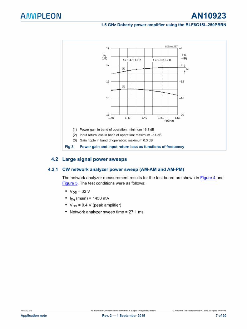
4.2.1 CW network analyzer power sweep (AM-AM and AM-PM)
The network analyzer measurement results for the test board are shown in Figure 4 and Figure 5. The test conditions were as follows:
• VDS = 32 V
• IDq (main) = 1450 mA
• VGS = 0.4 V (peak amplifier)
• Network analyzer sweep time = 27.1 ms
(1) Power gain in band of operation: minimum 16.3 dB
(2) Input return loss in band of operation: maximum 14 dB
(3) Gain ripple in band of operation: maximum 0.3 dB
Fig 3. Power gain and input return loss as functions of frequency
f (GHz)1.45 1.531.511.47 1.49
019aaa257
15
13
17
19
Gp(dB)
11
−12
−16
−8
−4
IRL(dB)
−20
(1) (3)
(2)
f = 1.476 GHz f = 1.511 GHz
AN10923#2 All information provided in this document is subject to legal disclaimers. © Ampleon The Netherlands B.V. 2015. All rights reserved.
Application note Rev. 2 — 1 September 2015 7 of 20
AN109231.5 GHz Doherty power amplifier using the BLF6G15L-250PBRN
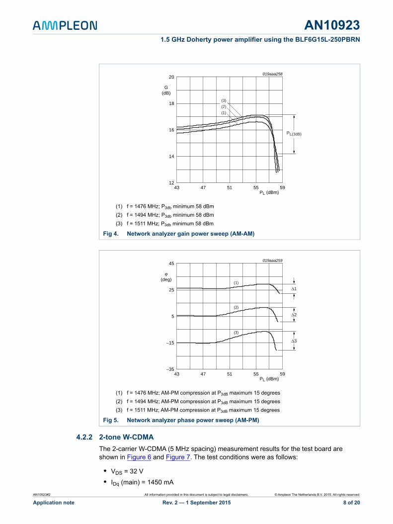
4.2.2 2-tone W-CDMA
The 2-carrier W-CDMA (5 MHz spacing) measurement results for the test board are shown in Figure 6 and Figure 7. The test conditions were as follows:
• VDS = 32 V
• IDq (main) = 1450 mA
(1) f = 1476 MHz; P3db minimum 58 dBm
(2) f = 1494 MHz; P3db minimum 58 dBm
(3) f = 1511 MHz; P3db minimum 58 dBm
Fig 4. Network analyzer gain power sweep (AM-AM)
(1) f = 1476 MHz; AM-PM compression at P3dB maximum 15 degrees
(2) f = 1494 MHz; AM-PM compression at P3dB maximum 15 degrees
(3) f = 1511 MHz; AM-PM compression at P3dB maximum 15 degrees
Fig 5. Network analyzer phase power sweep (AM-PM)
PL (dBm)43 595547 51
019aaa258
16
14
18
20
G(dB)
12
(1)
(2)
(3)
PL(3dB)
PL (dBm)43 595547 51
019aaa259
5
−15
25
45
ϕ(deg)
−35
(1)
(2)
(3)
Δ1
Δ2
Δ3
AN10923#2 All information provided in this document is subject to legal disclaimers. © Ampleon The Netherlands B.V. 2015. All rights reserved.
Application note Rev. 2 — 1 September 2015 8 of 20

AN109231.5 GHz Doherty power amplifier using the BLF6G15L-250PBRN
• VGS = 0.4 V (peak amplifier)
• 3 GPP, Test Model 1, 64 DPCH, PAR = 7.5 dB at 0.01% probability per carrier, 5 MHz carrier spacing
Efficiency at PL = 49 dBm minimum 36 %
Gain at PL = 49 dBm minimum 16 dB
(1) % efficiency at f = 1476 MHz
(2) % efficiency at f = 1494 MHz
(3) % efficiency at f = 1511 MHz
(4) dB gain at f = 1476 MHz
(5) dB gain at f = 1494 MHz
(6) dB gain at f = 1511 MHz
Fig 6. 2-carrier W-CDMA power sweep: gain as a function of output power
PL (dBm)38 545042 46
019aaa260
16
14
18
20
G(dB)
12
30
20
40
50
η(%)
10
(1)(2)(3)
(6)(5)(4)
PL = 49 dBm
AN10923#2 All information provided in this document is subject to legal disclaimers. © Ampleon The Netherlands B.V. 2015. All rights reserved.
Application note Rev. 2 — 1 September 2015 9 of 20
AN109231.5 GHz Doherty power amplifier using the BLF6G15L-250PBRN
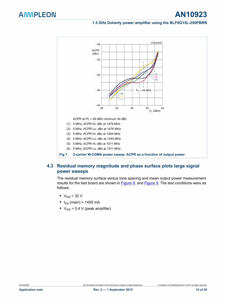
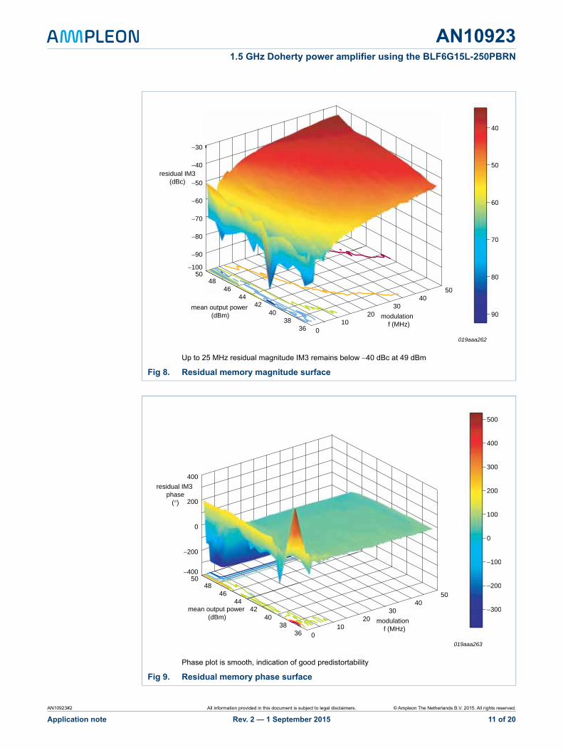
4.3 Residual memory magnitude and phase surface plots large signal power sweeps
The residual memory surface versus tone spacing and mean output power measurement results for the test board are shown in Figure 8. and Figure 9. The test conditions were as follows:
• VDS = 32 V
• IDq (main) = 1450 mA
• VGS = 0.4 V (peak amplifier)
ACPR at PL = 49 dBm minimum 34 dBc
(1) 5 MHz, ACPR Hi, dBc at 1476 MHz
(2) 5 MHz, ACPR Lo, dBc at 1476 MHz
(3) 5 MHz, ACPR Hi, dBc at 1494 MHz
(4) 5 MHz, ACPR Lo, dBc at 1494 MHz
(5) 5 MHz, ACPR Hi, dBc at 1511 MHz
(6) 5 MHz, ACPR Lo, dBc at 1511 MHz
Fig 7. 2-carrier W-CDMA power sweep: ACPR as a function of output power
PL (dBm)38 545042 46
019aaa261
−36
−40
−32
−28
ACPR(dBc)
−44
(4)(5)(6)
(1)(2)(3)
PL = 49 dBm
AN10923#2 All information provided in this document is subject to legal disclaimers. © Ampleon The Netherlands B.V. 2015. All rights reserved.
Application note Rev. 2 — 1 September 2015 10 of 20
AN109231.5 GHz Doherty power amplifier using the BLF6G15L-250PBRN
Up to 25 MHz residual magnitude IM3 remains below 40 dBc at 49 dBm
Fig 8. Residual memory magnitude surface
Phase plot is smooth, indication of good predistortability
Fig 9. Residual memory phase surface
−30
1038
residual IM3(dBc)
modulation f (MHz)
mean output power (dBm)
−40
−50
−60
−70
−80
−90
2030
4050
40
50
60
70
80
90
4244
4648
40
36 0
−10050
019aaa262
400
200
100
38
residual IM3 phase
(°)
modulation f (MHz)
mean output power (dBm)
−400
2030
4050
500
−3004244
4648
50
40
36
−200
−100
0
100
200
300
400
0
−200
019aaa263
AN10923#2 All information provided in this document is subject to legal disclaimers. © Ampleon The Netherlands B.V. 2015. All rights reserved.
Application note Rev. 2 — 1 September 2015 11 of 20
AN109231.5 GHz Doherty power amplifier using the BLF6G15L-250PBRN
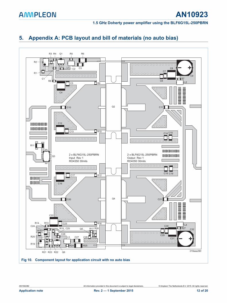
5. Appendix A: PCB layout and bill of materials (no auto bias)
Fig 10. Component layout for application circuit with no auto bias
2 x BLF6G15L-250PBRNOutput Rev 1RO4350 30mils
2 x BLF6G15L-250PBRNInput Rev 1RO4350 30mils
Q2
Q4 C21
C11
L2R7
C9
C8C7
C6
L4R27
R16
R12
R11
R10
R9
C4
R8C5
C10
C3C2L1
R6R5
L3
C23
C22
C16
C12
C17
C13
Q3
R13R14
R18
R19R25R24
R15 C25 R17 R26
C28C27
Q5 C32
C31
C30
C29
C18 C19
C14 C15
C24
C26
R21 R23 Q6R22
R20
Q1R4R3
R1
C1
R2
C20
019aaa280
AN10923#2 All information provided in this document is subject to legal disclaimers. © Ampleon The Netherlands B.V. 2015. All rights reserved.
Application note Rev. 2 — 1 September 2015 12 of 20
AN109231.5 GHz Doherty power amplifier using the BLF6G15L-250PBRN
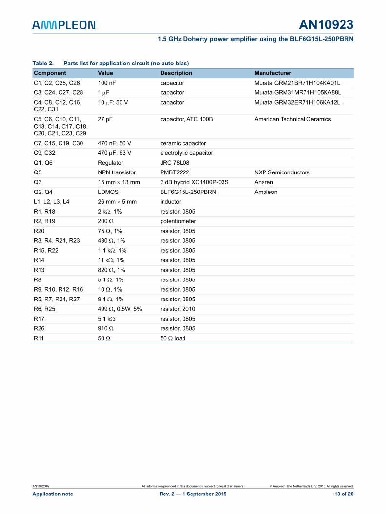
Table 2. Parts list for application circuit (no auto bias)
Component Value Description Manufacturer
C1, C2, C25, C26 100 nF capacitor Murata GRM21BR71H104KA01L
C3, C24, C27, C28 1 F capacitor Murata GRM31MR71H105KA88L
C4, C8, C12, C16, C22, C31
10 F; 50 V capacitor Murata GRM32ER71H106KA12L
C5, C6, C10, C11, C13, C14, C17, C18, C20, C21, C23, C29
27 pF capacitor, ATC 100B American Technical Ceramics
C7, C15, C19, C30 470 nF; 50 V ceramic capacitor
C9, C32 470 F; 63 V electrolytic capacitor
Q1, Q6 Regulator JRC 78L08
Q5 NPN transistor PMBT2222 NXP Semiconductors
Q3 15 mm 13 mm 3 dB hybrid XC1400P-03S Anaren
Q2, Q4 LDMOS BLF6G15L-250PBRN Ampleon
L1, L2, L3, L4 26 mm 5 mm inductor
R1, R18 2 k, 1% resistor, 0805
R2, R19 200 potentiometer
R20 75 , 1% resistor, 0805
R3, R4, R21, R23 430 , 1% resistor, 0805
R15, R22 1.1 k, 1% resistor, 0805
R14 11 k, 1% resistor, 0805
R13 820 , 1% resistor, 0805
R8 5.1 , 1% resistor, 0805
R9, R10, R12, R16 10 , 1% resistor, 0805
R5, R7, R24, R27 9.1 , 1% resistor, 0805
R6, R25 499 , 0.5W, 5% resistor, 2010
R17 5.1 k resistor, 0805
R26 910 resistor, 0805
R11 50 50 load
AN10923#2 All information provided in this document is subject to legal disclaimers. © Ampleon The Netherlands B.V. 2015. All rights reserved.
Application note Rev. 2 — 1 September 2015 13 of 20
AN109231.5 GHz Doherty power amplifier using the BLF6G15L-250PBRN
6. Appendix B: PCB layout and bill of materials with auto bias
Fig 11. Component layout for application circuit with auto bias
2 x BLF6G15L-250PBRNOutput Rev 1RO4350 30mils
2 x BLF6G15L-250PBRNInput Rev 1RO4350 30mils
Q2
Q4 C27
C13
L2
R7C11
VDS
C10C9
C8
L3R16
R15
R12
C22
C16
C17R11
R10
R9
C6 C7
C4
R8C5
C3C2L1
R6R5
C29
C30 C31
C28
C20
C14
C21
C26
C15
C12
Q3
R13
R14C35
C34
C33
019aaa281
C32
C24 C25
C18 C19
Q1R4R3
R1
C1
R2
C23
VDS
VDS
+Vln
VGSGND
autobias circuit
GND
AN10923#2 All information provided in this document is subject to legal disclaimers. © Ampleon The Netherlands B.V. 2015. All rights reserved.
Application note Rev. 2 — 1 September 2015 14 of 20
AN109231.5 GHz Doherty power amplifier using the BLF6G15L-250PBRN
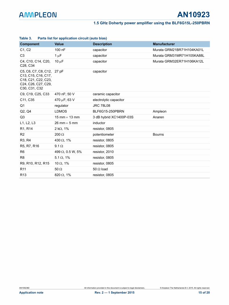
Table 3. Parts list for application circuit (auto bias)
Component Value Description Manufacturer
C1, C2 100 nF capacitor Murata GRM21BR71H104KA01L
C3 1 F capacitor Murata GRM31MR71H105KA88L
C4, C10, C14, C20, C28, C34
10 F capacitor Murata GRM32ER71H106KA12L
C5, C6, C7, C8, C12, C13, C15, C16, C17, C18, C21, C22, C23, C24, C26, C27, C29, C30, C31, C32
27 pF capacitor
C9, C19, C25, C33 470 nF; 50 V ceramic capacitor
C11, C35 470 F; 63 V electrolytic capacitor
Q1 regulator JRC 78L08
Q2, Q4 LDMOS BLF6G15-250PBRN Ampleon
Q3 15 mm 13 mm 3 dB hybrid XC1400P-03S Anaren
L1, L2, L3 26 mm 5 mm inductor
R1, R14 2 k, 1% resistor, 0805
R2 200 potentiometer Bourns
R3, R4 430 , 1% resistor, 0805
R5, R7, R16 9.1 resistor, 0805
R6 499 , 0.5 W, 5% resistor, 2010
R8 5.1 , 1% resistor, 0805
R9, R10, R12, R15 10 , 1% resistor, 0805
R11 50 50 load
R13 820 , 1% resistor, 0805
AN10923#2 All information provided in this document is subject to legal disclaimers. © Ampleon The Netherlands B.V. 2015. All rights reserved.
Application note Rev. 2 — 1 September 2015 15 of 20
AN109231.5 GHz Doherty power amplifier using the BLF6G15L-250PBRN
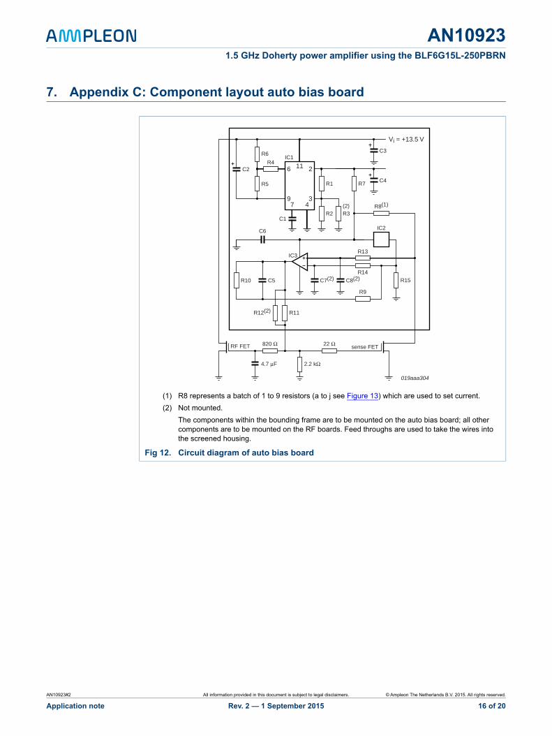
7. Appendix C: Component layout auto bias board
(1) R8 represents a batch of 1 to 9 resistors (a to j see Figure 13) which are used to set current.
(2) Not mounted.
The components within the bounding frame are to be mounted on the auto bias board; all other components are to be mounted on the RF boards. Feed throughs are used to take the wires into the screened housing.
Fig 12. Circuit diagram of auto bias board
019aaa304
4.7 μF 2.2 kΩ
RF FET sense FET820 Ω 22 Ω
R11R12(2)
C8(2) R15
R13
R9
IC2
IC1
R8(1)(2)
IC3
R14
C7(2)C5
C6
C2
R6
R5
R2 R3
R1 R7
C3
Vi = +13.5 V
R46
97 4
3
211
R10
C1
C4
AN10923#2 All information provided in this document is subject to legal disclaimers. © Ampleon The Netherlands B.V. 2015. All rights reserved.
Application note Rev. 2 — 1 September 2015 16 of 20
AN109231.5 GHz Doherty power amplifier using the BLF6G15L-250PBRN
[1] Not mounted
(1) Not mounted
Fig 13. Component layout of auto bias board
Table 4. Parts list for auto bias board
Component Value Description Manufacturer
C1 1 nF ceramic capacitor
C2 2.2 F electrolytic capacitor
C3 100 F electrolytic capacitor
C4 10 F electrolytic capacitor
C5 2.2 nF ceramic capacitor
C6 100 nF ceramic capacitor
IC1 - LT3011 Linear Technology
IC2 - LM4051 National Semiconductor
IC3 - LM7341 National Semiconductor
R1, R6 1 M resistor, 0603
R2, R3[1] 100 k resistor, 0603
R4 4.7 k resistor, 0603
R5 47 k resistor, 0603
R7 4.7 resistor, 1206
R8 57 up to 9 off; resistor, 0603
R9 2.7 k resistor, 0603
R10 56 k resistor, 0603
R11, R12[1] 6.8 k resistor, 0603
R13, R14, R15 10 k resistor, 0603
IC1
C2C1 C3
R8a R8b R8c
R8d R8e R8f
R8g R8h R8j
R6
R7
R5
R3(1)
(1)
(1)
(1)
R4
R2
R1
C4
C5C8
C7
R15
IC2
R13 R14
IC3
C8
R12R11
R10
R9
019aaa303
AN10923#2 All information provided in this document is subject to legal disclaimers. © Ampleon The Netherlands B.V. 2015. All rights reserved.
Application note Rev. 2 — 1 September 2015 17 of 20
AN109231.5 GHz Doherty power amplifier using the BLF6G15L-250PBRN
8. Abbreviations
Table 5. Abbreviations
Acronym Description
ACPR Adjacent Channel Power Ratio
CCDF Complementary Cumulative Distribution Function
CDMA Code Division Multiple Access
EDGE Enhanced Data rates for GSM Evolution
GSM Global System for Mobile communication
IS-95 Interim Standard 95
LDMOS Laterally Diffused Metal-Oxide Semiconductor
LDMOST Laterally Diffused Metal-Oxide Semiconductor Transistor
PAR Peak-to-Average power Ratio
RF Radio Frequency
UMTS Universal Mobile Telecommunications System
VSWR Voltage Standing-Wave Ratio
W-CDMA Wideband Code Division Multiple Access
AN10923#2 All information provided in this document is subject to legal disclaimers. © Ampleon The Netherlands B.V. 2015. All rights reserved.
Application note Rev. 2 — 1 September 2015 18 of 20
AN109231.5 GHz Doherty power amplifier using the BLF6G15L-250PBRN
9. Legal information
9.1 Definitions
Draft — The document is a draft version only. The content is still under internal review and subject to formal approval, which may result in modifications or additions. Ampleon does not give any representations or warranties as to the accuracy or completeness of information included herein and shall have no liability for the consequences of use of such information.
9.2 Disclaimers
Limited warranty and liability — Information in this document is believed to be accurate and reliable. However, Ampleon does not give any representations or warranties, expressed or implied, as to the accuracy or completeness of such information and shall have no liability for the consequences of use of such information. Ampleon takes no responsibility for the content in this document if provided by an information source outside of Ampleon.
In no event shall Ampleon be liable for any indirect, incidental, punitive, special or consequential damages (including - without limitation - lost profits, lost savings, business interruption, costs related to the removal or replacement of any products or rework charges) whether or not such damages are based on tort (including negligence), warranty, breach of contract or any other legal theory.
Notwithstanding any damages that customer might incur for any reason whatsoever, Ampleon’ aggregate and cumulative liability towards customer for the products described herein shall be limited in accordance with the Terms and conditions of commercial sale of Ampleon.
Right to make changes — Ampleon reserves the right to make changes to information published in this document, including without limitation specifications and product descriptions, at any time and without notice. This document supersedes and replaces all information supplied prior to the publication hereof.
Suitability for use — Ampleon products are not designed, authorized or warranted to be suitable for use in life support, life-critical or safety-critical systems or equipment, nor in applications where failure or malfunction of an Ampleon product can reasonably be expected to result in personal injury, death or severe property or environmental damage. Ampleon and its suppliers accept no liability for inclusion and/or use of Ampleon products in such equipment or applications and therefore such inclusion and/or use is at the customer’s own risk.
Applications — Applications that are described herein for any of these products are for illustrative purposes only. Ampleon makes no representation or warranty that such applications will be suitable for the specified use without further testing or modification.
Customers are responsible for the design and operation of their applications and products using Ampleon products, and Ampleon accepts no liability for any assistance with applications or customer product design. It is customer’s sole responsibility to determine whether the Ampleon product is suitable and fit for the customer’s applications and products planned, as well as for the planned application and use of customer’s third party customer(s). Customers should provide appropriate design and operating safeguards to minimize the risks associated with their applications and products.
Ampleon does not accept any liability related to any default, damage, costs or problem which is based on any weakness or default in the customer’s applications or products, or the application or use by customer’s third party customer(s). Customer is responsible for doing all necessary testing for the customer’s applications and products using Ampleon products in order to avoid a default of the applications and the products or of the application or use by customer’s third party customer(s). Ampleon does not accept any liability in this respect.
Export control — This document as well as the item(s) described herein may be subject to export control regulations. Export might require a prior authorization from competent authorities.
9.3 TrademarksNotice: All referenced brands, product names, service names and trademarks are the property of their respective owners.
Any reference or use of any ‘NXP’ trademark in this document or in or on thesurface of Ampleon products does not result in any claim, liability orentitlement vis-à-vis the owner of this trademark. Ampleon is no longer part ofthe NXP group of companies and any reference to or use of the ‘NXP’ trademarks will be replaced by reference to or use of Ampleon’s own Any reference or use of any ‘NXP’ trademark in this document or in or on thesurface of Ampleon products does not result in any claim, liability orentitlement vis-à-vis the owner of this trademark. Ampleon is no longer part ofthe NXP group of companies and any reference to or use of the ‘NXP’trademarks will be replaced by reference to or use of Ampleon’s own trademarks.
AN10923#2 All information provided in this document is subject to legal disclaimers. © Ampleon The Netherlands B.V. 2015. All rights reserved.
Application note Rev. 2 — 1 September 2015 19 of 20
AN109231.5 GHz Doherty power amplifier using the BLF6G15L-250PBRN
10. Contents
1 Introduction . . . . . . . . . . . . . . . . . . . . . . . . . . . . 3
2 Circuit description . . . . . . . . . . . . . . . . . . . . . . . 3
3 Design and Tuning. . . . . . . . . . . . . . . . . . . . . . . 43.1 Design of the single stage amplifiers . . . . . . . . 53.2 Doherty design . . . . . . . . . . . . . . . . . . . . . . . . . 53.3 Tuning. . . . . . . . . . . . . . . . . . . . . . . . . . . . . . . . 63.4 Transistor biasing . . . . . . . . . . . . . . . . . . . . . . . 6
4 Test results . . . . . . . . . . . . . . . . . . . . . . . . . . . . . 64.1 Network analyzer frequency sweep . . . . . . . . . 64.2 Large signal power sweeps . . . . . . . . . . . . . . . 74.2.1 CW network analyzer power sweep (AM-AM and
AM-PM) . . . . . . . . . . . . . . . . . . . . . . . . . . . . . . 74.2.2 2-tone W-CDMA . . . . . . . . . . . . . . . . . . . . . . . . 84.3 Residual memory magnitude and phase surface
plots large signal power sweeps. . . . . . . . . . . 10
5 Appendix A: PCB layout and bill of materials (no auto bias) . . . . . . . . . . . . . . . . . . . . . . . . . . 12
6 Appendix B: PCB layout and bill of materials with auto bias. . . . . . . . . . . . . . . . . . . . . . . . . . 14
7 Appendix C: Component layout auto bias board. . . . . . . . . . . . . . . . . . . . . . . . . . . . . . . . . 16
8 Abbreviations. . . . . . . . . . . . . . . . . . . . . . . . . . 18
9 Legal information. . . . . . . . . . . . . . . . . . . . . . . 199.1 Definitions. . . . . . . . . . . . . . . . . . . . . . . . . . . . 199.2 Disclaimers . . . . . . . . . . . . . . . . . . . . . . . . . . . 199.3 Trademarks. . . . . . . . . . . . . . . . . . . . . . . . . . . 19
10 Contents . . . . . . . . . . . . . . . . . . . . . . . . . . . . . . 20
© Ampleon The Netherlands B.V. 2015. All rights reserved.
For more information, please visit: http://www.ampleon.comFor sales office addresses, please visit: http://www.ampleon.com/sales
Date of release: 1 September 2015
Document identifier: AN10923#2
Please be aware that important notices concerning this document and the product(s)described herein, have been included in section ‘Legal information’.