Embed Size (px)
Citation preview

AN101516HV785: Programmable Lead Acid Battery Charger
Features
• User-configurable battery charger for Lead battery packs
• Based on PIC16F785 with integrated shunt regulator
• Firmware and support tools for easy design
• 10-bit ADC for voltage, current and temperature measurement:
- Accurate Voltage Regulation (+/-1%)- Accurate Current Regulation (+/-5%)
• Advanced Charge Algorithms:
- Chemistry dependent End-of-Charge determination
- Charge qualification to detect shorted, damaged or heated cells
- Precharge for deeply discharged cells- Configurable overtemperature and
overvoltage charge suspension- Charge termination at user-specified
minimum current or time-out- Configurable charge status display via two
LEDs• Maximum integration for optimal size:
- Integrated voltage regulator
- Internal 8 MHz clock oscillator- High-Frequency Switch mode charging –
configurable switching frequency up to 500 kHz
Applications
• Single-Cell and Multi-Cell Lead Battery Chargers• Notebook Computers• Personal Data Assistants• Cellular Telephones• Digital Still Cameras• Camcorders• Portable Audio Products• Bluetooth® Devices
Pin Description
2
34
567
8
9
20
19
1817
161514
13
12
16H
V78
5
20-Pin PDIP, SOIC, SSOP
1
10 11
VDD
LED2
VIN
RESETCTRLOUT
CHGOUT
LOOPFBKLOOPIN
CTRLIN
LED1
VSS
TEMP
VOVP
SHDNCHGFBKBATIDIFBOUT
IFBINA
IFBINB
HVOUT
© 2006 Microchip Technology Inc. DS01015A-page 1

AN1015
USING THE 16HV785
Product Overview
The 16HV785 provides an unprecedented level of con-figurability for charging lead battery packs. Its precise,10-bit Analog-to-Digital converter and high-frequencyPulse-Width Modulator enable the 16HV785 to provideoptimum control of charging algorithms for lead batterychemistries. Special features include an internal voltageregulator and an internal clock oscillator that reduceexternal component count. The 16HV785 can be config-ured as either a Switch mode or a linear charger. InSwitch mode, it will support either primary or secondaryside control. In Linear mode, it can be designed intoapplications requiring low-power supply noise.
MULTI-STEP CHARGING
To insure the proper treatment of lead chemistriesduring extreme temperature and voltage conditions,multi-step charging is required. The 16HV785 starts thecharging cycle upon sensing the presence of a batterypack and a valid charging supply. During chargequalification, the battery’s temperature and voltage aremeasured to determine the appropriate initial state.The initial states include Charge Suspend, Prechargeand Current Regulation. Charge Suspend haltscharging when the user-defined preset conditions forcharging are not met. Precharge allows for the recov-ery of deeply discharged batteries by applying a lowcharge (or C) rate. Current Regulation providesconstant current, voltage limited charge. Uponreaching the target voltage during Current Regulation,the Voltage Regulation state is entered. Chargingcontinues at a constant voltage until the currentdecreases to the user-specified minimum currentthreshold. The user-specified minimum currentthreshold can be configured for various chargingtemperatures. At this threshold, charging is terminatedand the End-of-Charge state is reached.
USER CONFIGURABLE PARAMETERS
The 16HV785 supports user-configurable parametersthat allow for customizing the charging profile withoutchanging the charger’s hardware design. This featureallows for the maximum reuse of hardware, thusreducing time-to-market. These parameters include:
• Battery Temperature:- Minimum/maximum temperature for charge
initiation- Maximum temperature allowed during charge
• Battery Voltage:- Minimum/maximum voltage for charge
initiation- Target voltage during Voltage Regulation- Voltage at which the charger will restart
charging after completion of a valid charge cycle
• Charge Current:- Target current during Current Regulation
- Taper current threshold for End-of-Charge during Voltage Regulation
- Target current during Precharge• Time:
- Precharge time limit
- Current Regulation time limit- Voltage Regulation time limit
• Status Display:
- Duty cycle for the two LEDs denoting charge states can be modified
These parameters are configured through thePowerTool™ 200 Development Software for the16HV785.
SPECIAL FEATURES
The 16HV785 includes a voltage regulator, a voltagereference, an internal clock oscillator and ahigh-frequency Pulse-Width Modulator.
• The internal voltage regulator has a maximum input voltage of 18V and eliminates the need for external references.
• The precise, internal 8 MHz clock oscillator eliminates the need for external oscillator circuits.
• The high-speed Pulse-Width Modulator is used for power regulation and can support frequencies up to 500 kHz.
• In-circuit configurability utilizing on-board EEPROM.
DS01015A-page 2 © 2006 Microchip Technology Inc.

AN1015
TABLE 1: PINOUT DESCRIPTION
Pin Pin Name Pin Type Input Type Output Type Description
1 VDD Supply Power — Supply voltage
2 LED2 O — CMOS Status indicator
3 VIN I Analog — Battery voltage input
4 RESET I ST — Reset
5 CTRLOUT O — CMOS PWM output for setting current level
6 CHGOUT O — CMOS PWM output to a buck converter for charge control
7 LOOPFBK I Analog — Current feedback loop
8 LOOPIN I Analog — Current feedback loop input
9 CTRLIN I Analog — Current level control
10 LED1 O — CMOS Status indicator
11 HVOUT O — HVOD High-voltage, open-drain output pin (optional)
12 IFBINB I Analog — Current feedback input pin B used for current scaling
13 IFBINA I Analog — Current feedback input pin A used for current scaling
14 IFBOUT O — Analog Current feedback output
15 BATID I Analog — Battery ID select
16 CHGFBK I Analog — Charge control feedback
17 SHDN O — Analog Shutdown signal, active-low
18 VOVP I Analog — Overvoltage protection
19 TEMP I Analog — Battery temperature input
20 VSS Supply Power — Supply ground
Legend: I = Input, O = Output, ST = Schmitt Trigger Input Buffer, HVOD = High-Voltage Open-Drain
© 2006 Microchip Technology Inc. DS01015A-page 3
AN1015
16HV785 HARDWARE OVERVIEW
The 16HV785 is a configurable, Switch mode chargerwhich is comprised of a PIC16F microcontroller coreand precise analog circuitry. This section explores thehardware features in relation to generic Switch modecharging. The 16HV785 hardware is a PIC16F785device with an integrated shunt regulator, to allow thedevice to be powered directly from a battery stack, orfrom charger voltage. It is available in a 20-pin PDIP,SOIC or SSOP package. See the PIC16F785 datasheet for more hardware description. Hardwarefeatures include:
• Oscillator
• Power-Saving Sleep mode• Power-on Reset (POR)• Brown-out Reset (BOR)
• High-Endurance Flash/EEPROM Cell:- 100,000 write Flash endurance- 1,000,000 write EEPROM endurance
- Flash/Data EEPROM retention: > 40 years• High-Speed Comparator module with:
- Two independent analog comparators
• Operational Amplifier module with two independent op amps
• Two-Phase Asynchronous Feedback PWM• Voltage Regulator• 10-bit A/D Converter
• In-Circuit Serial Programming™ (ICSP™) via two pins
Hardware Features
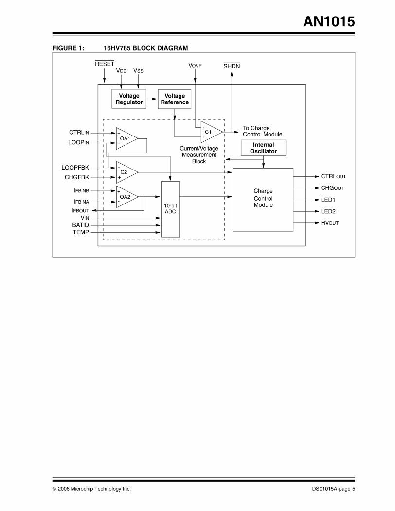
The 16HV785 features are well-suited for Switch modebattery charging. The 16HV785 device’s block diagram(Figure 1) is to be used in conjunction with the Switchmode charger example (Figure 10, page 9).
• Current/Voltage Measurement Block – The Current/Voltage Measurement Block consists of a 10-bit Analog-to-Digital converter, operational amplifiers and a comparator. The output of this block is fed into the charge control module. Please refer to Figure 1.
The inputs into this block are to be connected asdescribed in Figure 10. The following signals areinputs into this block:
- LOOPFBK: to comparator- LOOPIN: to op amp and ADC
- CTRLIN: to op amp- IFBINB: to op amp- IFBINA: to op amp
- BATID: to ADC- TEMP: to ADC- CHGFBK: to comparator
The following signals are outputs from this block:
- IFBOUT: from op amp
• Charge Control Module – The charge control module generates a Pulse-Width Modulated signal called CHGOUT. Its frequency is config-urable and can be set up to 1 MHz. This signal is connected to an external DC/DC buck converter.
• Voltage Regulator – The integrated voltage regulator is designed to work with unregulated DC supplies.
• The precise internal 8 MHz clock oscillator eliminates the need for external oscillator circuits.
• In-circuit configurability utilizing 256 bytes of on-board EEPROM.
• Power on Reset – The POR insures the proper start-up of the 16HV785 when voltage is applied to VDD.
• Brown-out Reset – The BOR is activated when the input voltage falls to 2.1V; the 16HV785 is reset.
DS01015A-page 4 © 2006 Microchip Technology Inc.
AN1015
FIGURE 1: 16HV785 BLOCK DIAGRAM
ChargeControl
CTRLOUT
CHGOUT
LED2
HVOUT
InternalOscillator
VoltageRegulator
Current/VoltageMeasurement
Block
CTRLIN
LOOPIN
LOOPFBK
CHGFBK
IFBINB
IFBINA
TEMP
IFBOUT
VDD VSS
VoltageReference
VIN
OA1+
-
C2-
+
OA2+
-10-bitADC
Module
RESET
C1-
+
VOVP
LED1
SHDN
To ChargeControl Module
BATID
© 2006 Microchip Technology Inc. DS01015A-page 5
AN1015
REFERENCE SCHEMATIC
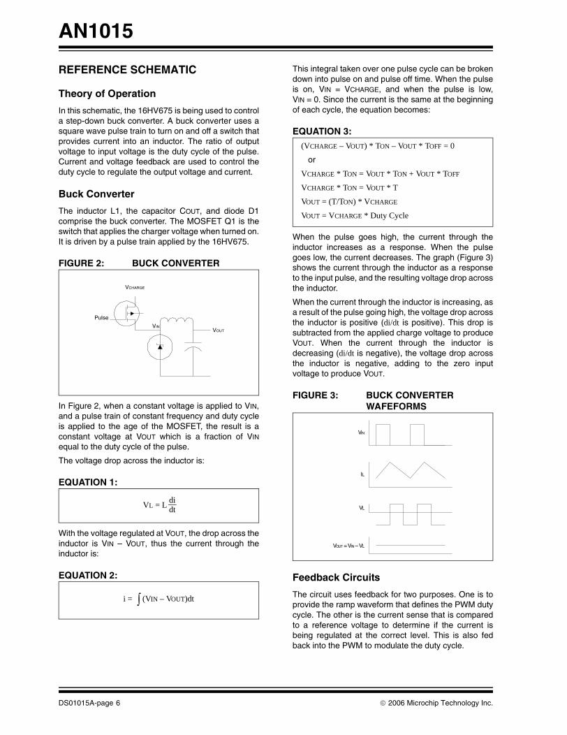
Theory of Operation
In this schematic, the 16HV675 is being used to controla step-down buck converter. A buck converter uses asquare wave pulse train to turn on and off a switch thatprovides current into an inductor. The ratio of outputvoltage to input voltage is the duty cycle of the pulse.Current and voltage feedback are used to control theduty cycle to regulate the output voltage and current.
Buck Converter
The inductor L1, the capacitor COUT, and diode D1comprise the buck converter. The MOSFET Q1 is theswitch that applies the charger voltage when turned on.It is driven by a pulse train applied by the 16HV675.
FIGURE 2: BUCK CONVERTER
In Figure 2, when a constant voltage is applied to VIN,and a pulse train of constant frequency and duty cycleis applied to the age of the MOSFET, the result is aconstant voltage at VOUT which is a fraction of VIN
equal to the duty cycle of the pulse.
The voltage drop across the inductor is:
EQUATION 1:
With the voltage regulated at VOUT, the drop across theinductor is VIN – VOUT, thus the current through theinductor is:
EQUATION 2:
This integral taken over one pulse cycle can be brokendown into pulse on and pulse off time. When the pulseis on, VIN = VCHARGE, and when the pulse is low,VIN = 0. Since the current is the same at the beginningof each cycle, the equation becomes:
EQUATION 3:
When the pulse goes high, the current through theinductor increases as a response. When the pulsegoes low, the current decreases. The graph (Figure 3)shows the current through the inductor as a responseto the input pulse, and the resulting voltage drop acrossthe inductor.
When the current through the inductor is increasing, asa result of the pulse going high, the voltage drop acrossthe inductor is positive (di/dt is positive). This drop issubtracted from the applied charge voltage to produceVOUT. When the current through the inductor isdecreasing (di/dt is negative), the voltage drop acrossthe inductor is negative, adding to the zero inputvoltage to produce VOUT.
FIGURE 3: BUCK CONVERTER WAFEFORMS
Feedback Circuits
The circuit uses feedback for two purposes. One is toprovide the ramp waveform that defines the PWM dutycycle. The other is the current sense that is comparedto a reference voltage to determine if the current isbeing regulated at the correct level. This is also fedback into the PWM to modulate the duty cycle.
VCHARGE
VOUTVIN
Pulse
VL = Ldidt
∫ (VIN – VOUT)dti =
(VCHARGE – VOUT) * TON – VOUT * TOFF = 0
or
VCHARGE * TON = VOUT * TON + VOUT * TOFF
VCHARGE * TON = VOUT * T
VOUT = (T/TON) * VCHARGE
VOUT = VCHARGE * Duty Cycle
VIN
IL
VL
VOUT = VIN – VL
DS01015A-page 6 © 2006 Microchip Technology Inc.

AN1015
RAMP FEEDBACK
The CHGFBK pin (pin 16) receives the ramp sawtoothwaveform that controls the duty cycle of the PWM signal.This sawtooth needs to be generated externally by anRC network connected to the PWM output. The RC net-work uses the frequency of the PWM to generate thesawtooth waveform. When the PWM is triggered high,the sawtooth starts to ramp up. When the sawtoothreaches a certain point (determined internally by refer-ence voltage and current feedback), the PWM output issent low, also driving the sawtooth low. The sawtoothstarts up again when the internal oscillator sends thePWM high again.
The RC circuit can be placed on the output of the PWMsignal. A clamping diode can be used to control thetotal voltage drop.
FIGURE 4: SAWTOOTH GENERATOR
The voltage at CHGFBK will ramp up when the PWMoutput at CHGOUT triggers high. When the ramp atCHGFBK exceeds the internal comparator level ofreference voltage, the PWM will trigger CHGOUT low.The constant frequency sawtooth will determine thepulse width as a function of internal reference voltage.
FIGURE 5: SAWTOOTH AND PWM WAVEFORMS
CURRENT FEEDBACK
The aforementioned reference voltage is determined bycurrent feedback in order to regulate the current. A sec-ond PWM, which is under firmware control, is used tocreate a DC level to which to compare the sensed cur-rent. The voltage drop across a current sense resistor isapplied to pin 13 (IFBINA) and is internally amplified by anop amp. The output of this op amp is available on pin 14(IFBOUT). The output on pin 14 is then fed into pin 8(LOOPIN) which is the input to another op amp. Theother input of this op amp is a DC level that is created bythe firmware controlled PWM. The firmware controlledPWM is output on pin 5 (CTRLOUT) and fed into an RCcircuit whose time constant is high enough to create arough DC level. This DC level will vary with the dutycycle of the firmware controlled PWM. This DC level isthen applied to pin 9 (CTRLIN). This DC level is com-pared to the current feedback by op amp 1. The outputof op amp 1 is fed to the main internal comparator whereit is compared to the sawtooth waveform to determinethe duty cycle of the main PWM, which regulates currentthrough the buck converter.
FIGURE 6: FEEDBACK DIAGRAM
The actual circuit implementation, including op ampfeedback RC networks, is shown in Figure 7.
FIGURE 7: FEEDBACK CIRCUIT
pin 6: CHGOUT
pin 16: CHGFBK
Internal Oscillator
Sawtooth Triggered by Oscillator
PWM Triggered by Sawtooth
Level at whichInternal ComparatorSwitches PWM Low
Sense ResistorVoltage
Constant ReferenceVoltage from Firmware
Controlled PWM
SawtoothFeedback Signal
PWM Output
RSENSE
RIL
SawtoothFeedbackSignal
PWM Output
FirmwareControlled PWM
DC ReferenceVoltage
Amplified Current Feedback
Current Sense
16
9
814
13
12
6
5
7
© 2006 Microchip Technology Inc. DS01015A-page 7
AN1015
Power Supply Shunt Regulator
The 16HV785 has a built-in shunt regulator allowingthe device to be powered directly by the charging volt-age. The integrated voltage regulator is designed towork with unregulated DC supplies. While there is, the-oretically, no limit to the charging voltage, there areguidelines that should be followed. A series limitingresistor (RVDD) should be placed between the unregu-lated supply and the VDD pin. The value for this seriesresistor (RVDD) must be between RMIN and RMAX asshown in Equation 4:
EQUATION 4:
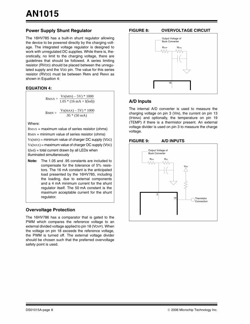
Overvoltage Protection
The 16HV786 has a comparator that is gated to thePWM which compares the reference voltage to anexternal divided voltage applied to pin 18 (VOVP). Whenthe voltage on pin 18 exceeds the reference voltage,the PWM is turned off. The external voltage dividershould be chosen such that the preferred overvoltagesafety point is used.
FIGURE 8: OVERVOLTAGE CIRCUIT
A/D Inputs
The internal A/D converter is used to measure thecharging voltage on pin 3 (VIN), the current on pin 13(IFBINA) and optionally, the temperature on pin 19(TEMP) if there is a thermistor present. An externalvoltage divider is used on pin 3 to measure the chargevoltage.
FIGURE 9: A/D INPUTS
Where:RMAX = maximum value of series resistor (ohms)
RMIN = minimum value of series resistor (ohms)Vs(MIN) = minimum value of charger DC supply (VDC)Vs(MAX) = maximum value of charger DC supply (VDC)
I(led) = total current drawn by all LEDs when illuminated simultaneously
Note: The 1.05 and .95 constants are included tocompensate for the tolerance of 5% resis-tors. The 16 mA constant is the anticipatedload presented by the 16HV785, includingthe loading, due to external componentsand a 4 mA minimum current for the shuntregulator itself. The 50 mA constant is themaximum acceptable current for the shuntregulator.
VS(MIN) – 5V) * 1000RMAX =
1.05 * (16 mA + I(led))
Vs(MAX) – 5V) * 1000RMIN =
.95 * (50 mA)
Output Voltage ofBuck Converter
ROVP ROVL
18
Output Voltage ofBuck Converter
RVH RVL
3
VDD
ThermistorConnection
19
DS01015A-page 8 © 2006 Microchip Technology Inc.
AN1015
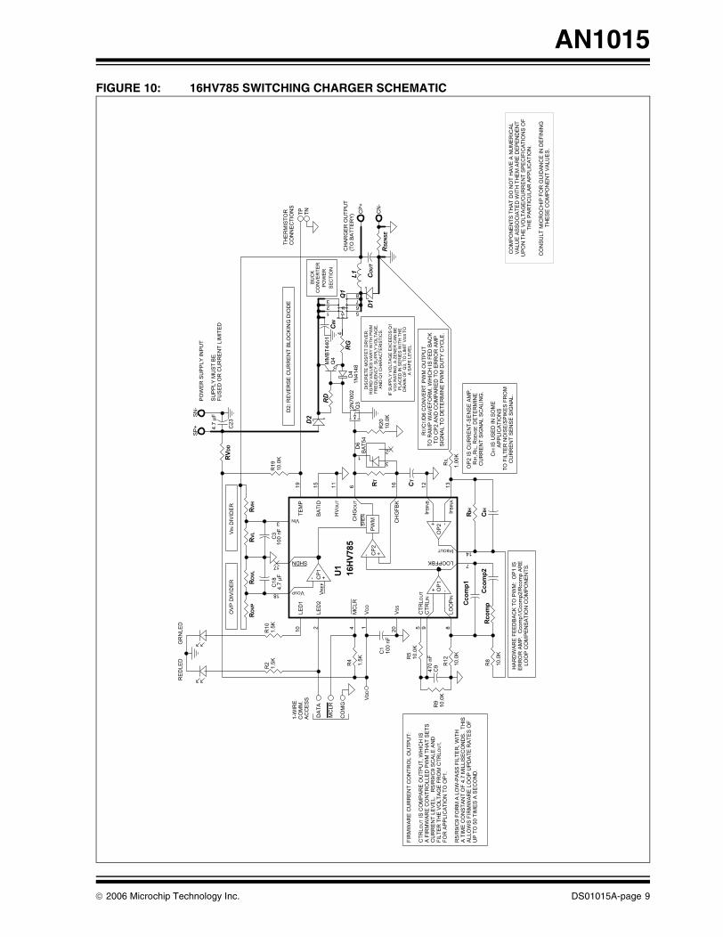
FIGURE 10: 16HV785 SWITCHING CHARGER SCHEMATIC
RS
EN
SE
VD
D
C1
100
nF
R4
1.5K
RIH
RIL
1.00
K
Cco
mp1
Cco
mp2
Rco
mp
R8
10.0
K
R5
10.0
K
R9
10.0
K
CT
RT
RV
DD
RV
LR
OV
L
R20
10.0
K
R19
10.0
K
GR
NLE
DR
ED
LED
R2
1.5K
R10
1.5K
31
2D6
BA
T54
L1
C3
100
nF
RO
VP
RV
H
D2
CO
UT
CIN
C23
4.7
μF
C18
D1
5
4
123
678
Q1
VD
D1
LED
22
VIN3
MC
LR4
CT
RLO
UT
5
CH
GO
UT
6
LOOPFBK 7
LOO
PIN
8
CT
RLI
N9
LED
110
HV
OU
T11
IFB
INB
12
IFB
INA
13
IFBOUT 14
BA
TID
15
CH
GF
BK
16
SHDN17
TE
MP
19
VOVP18
VS
S20
+ -O
P2
+ -OP
1
+- CP
2P
WM
+- CP
1V
RE
F
SH
DN
U1
16H
V78
5
CN
-
CP
+
SP
+S
N-
TP
TN
DA
TA
MC
LR
CO
MG
1-W
IRE
CO
MM
.A
CC
ES
S
PO
WE
R S
UP
PLY
INP
UT
CH
AR
GE
R O
UT
PU
T(T
O B
AT
TE
RY
)
TH
ER
MIS
TO
R
SU
PP
LY M
US
T B
EF
US
ED
OR
CU
RR
EN
T L
IMIT
ED
OV
P D
IVID
ER
VIN
DIV
IDE
R
D2:
RE
VE
RS
E C
UR
RE
NT
BLO
CK
ING
DIO
DE
CO
NN
EC
TIO
NS
R12
10.0
K
Q3
2N70
02
Q4
MM
BT
4401
RG
D4
1N41
48
RD
C9
470
nF
FIR
MW
AR
E C
UR
RE
NT
CO
NT
RO
L O
UT
PU
T:
CT
RLO
UT IS
CO
MP
AR
E O
UT
PU
T, W
HIC
H IS
A F
IRM
WA
RE
CO
NT
RO
LLE
D P
WM
TH
AT
SE
TS
CU
RR
EN
T L
EV
EL.
R
5/R
9/C
9 S
CA
LE A
ND
FIL
TE
R T
HE
VO
LTA
GE
FR
OM
CT
RL O
UT,
FO
R A
PP
LIC
AT
ION
TO
OP
1.
R5/
R9/
C9
FO
RM
A L
OW
-PA
SS
FIL
TE
R, W
ITH
A T
IME
CO
NS
TA
NT
OF
4.7
MIL
LIS
EC
ON
DS
. T
HIS
ALL
OW
S F
IRM
WA
RE
LO
OP
UP
DA
TE
RA
TE
S O
FU
P T
O 5
0 T
IME
S A
SE
CO
ND
.O
P2
IS C
UR
RE
NT
-SE
NS
E A
MP
.R
IH, R
IL, R
SE
NS
E D
ET
ER
MIN
EC
UR
RE
NT
SIG
NA
L S
CA
LIN
G.
CIH
IS U
SE
D IN
SO
ME
AP
PLI
CA
TIO
NS
TO
FIL
TE
R N
OIS
E/S
PIK
ES
FR
OM
CU
RR
EN
T S
EN
SE
SIG
NA
L.
HA
RD
WA
RE
FE
ED
BA
CK
TO
PW
M:
OP
1 IS
E
RR
OR
AM
P.
Cco
mp1
/Cco
mp2
/Rco
mp
AR
ELO
OP
CO
MP
EN
SA
TIO
N C
OM
PO
NE
NT
S.
RT/C
T/D
6 C
ON
VE
RT
PW
M O
UT
PU
TT
O R
AM
P W
AV
EF
OR
M, W
HIC
H IS
FE
D B
AC
KT
O C
P2
AN
D C
OM
PA
RE
D T
O E
RR
OR
AM
PS
IGN
AL
TO
DE
TE
RM
INE
PW
M D
UT
Y C
YC
LE.
CIH
BU
CK
CO
NV
ER
TE
RP
OW
ER
SE
CT
ION
DIS
CR
ET
E M
OS
FE
T D
RIV
ER
:R
G/R
D V
ALU
ES
VA
RY
WIT
H P
WM
FR
EQ
UE
NC
Y, S
UP
PLY
VO
LTA
GE
, A
ND
Q1
CH
AR
AC
TE
RIS
TIC
S.
IF S
UP
PLY
VO
LTA
GE
EX
CE
ED
S Q
1 V
GS
RA
TIN
G, A
ZE
NE
R C
AN
BE
PLA
CE
D IN
SE
RIE
S W
ITH
TH
ED
RA
IN O
F Q
3, T
O L
IMIT
VG
S T
OA
SA
FE
LE
VE
L.
CO
MP
ON
EN
TS
TH
AT
DO
NO
T H
AV
E A
NU
ME
RIC
AL
VA
LUE
AS
SO
CIA
TE
D W
ITH
TH
EM
AR
E D
EP
EN
DE
NT
UP
ON
TH
E V
OLT
AG
E/C
UR
RE
NT
SP
EC
IFIC
AT
ION
S O
F T
HE
PA
RT
ICU
LAR
AP
PLI
CA
TIO
N.
CO
NS
ULT
MIC
RO
CH
IP F
OR
GU
IDA
NC
E IN
DE
FIN
ING
TH
ES
E C
OM
PO
NE
NT
VA
LUE
S.
4.7
μF
© 2006 Microchip Technology Inc. DS01015A-page 9
AN1015
FUNCTIONAL DESCRIPTION: LEAD CHEMISTRY
Lead Charging
To ensure the proper treatment of lead chemistriesduring extreme temperature and voltage conditions,multi-step charging is required. The 16HV785 measureskey voltage, temperature and time parameters. Itcompares them to user-defined voltage, temperatureand time limits.
CHARGE PENDING STATE – BEGINNING THE CHARGE CYCLE
The 16HV785 is initially set in the Charge Pendingstate. In this state, the presence of a battery pack mustbe sensed in order to begin the charging cycle. The16HV785 comes up in the Charge Pending state aftera Reset, independent of the previous state.
CHARGE QUALIFICATION STATE
During Charge Qualification, the battery’s temperatureand voltage are measured to determine the nextcharging state. There are two possible next states.
1. If Mode3<0> is set to ‘1’, then skip to FloatCharge state is selected. Charge Qualificationwill always jump directly to Float Charge state.
2. If Mode3<0> is set to ‘0’, then skip to FloatCharge state is deselected. Charge Qualifica-tion will always progress to Current Regulationstate.
CURRENT REGULATION STATE
The Current Regulation state is entered from ChargeQualification state. Battery charging is initiated. This stateprovides constant current, voltage limited charging. Thecharge current is referred to as ChargeCurr or the regu-lation current. While the current is applied, the battery’svoltage increases until it reaches a voltage limit referredto as the regulation voltage. For lead batteries, thischarge voltage can vary with temperature. Coldertemperatures can allow the battery to use higher charg-ing voltages. To take advantage of this, Mode3<1> canbe set to ‘0’. This uses a look-up table of charge voltagesas a function of temperature from the parametersV_CHG_0..9 (voltage) and T_VLUT_0..8 (temperature).When Mode3<1> is set to ‘1’, a constant charge voltageis used from the parameter ChargeVolt. Chargingcontinues, during which battery voltage and temperatureare monitored. There are two possible next states.
1. If the battery’s voltage reaches or exceeds thevoltage limit, then the next state is VoltageRegulation.
2. If the time in the Current Regulation stateexceeds the time limit (TimeoutCCState), thenthe next state is Charge Suspend.
VOLTAGE REGULATION STATE
Voltage Regulation provides charging at a constantvoltage while the charge current decreases (or tapers)to the user-specified minimum current threshold(EOCCurrent). There are three possible next states.
1. When the charge current reaches the taper cur-rent threshold for End-of-Charge (EOCCurrent),the battery’s voltage remains at the regulatedvoltage value and Float mode is deselected(Mode3<3> = 0), then the battery has reachedthe Charge Cycle Complete state.
2. When the charge current reaches the taper cur-rent threshold for End-of-Charge (EOCCurrent),the battery’s voltage remains at the regulatedvoltage value and Float mode is selected(Mode3<3> = 1), then the battery has reachedthe Float Charge state.
3. If the time in the Voltage Regulation stateexceeds the time limit (TimeoutCVState), thenthe next state is Charge Suspend.
FLOAT CHARGE STATE
In the Float Charge state, a lower charge target voltageis applied. As in Current Regulation state, the targetvoltage can be a constant or can vary with temperature.When Mode3<1> is set to ‘0’, the charger uses a look-uptable of float charge voltages as a function of temperaturefrom the parameters V_FLT_0..9 (voltage) andT_VLUT_0..8 (temperature). When Mode3<1> is set to‘1’, a constant charge voltage is used from the parameterFloatVolt. The resulting taper current is measured andcompared against EOCCurrent. This helps to maintain afull charge. There is only one possible next state and thatis Charge Cycle Complete. Charge Cycle Complete isentered when the voltage reaches the float voltage targetand the current tapers to less than EOCCurrent, or thefloat timer, TimeoutFLState, expires.
CHARGE SUSPEND STATE
In the Charge Suspend state, no current is applied tothe battery pack. There is only one possible next state.If Mode3<5> is set to ‘1’, then suspend forever isselected. Suspend mode will be active until the batteryis removed. If Mode3<5> is set to ‘0’, then Suspendmode will be active until the suspend timer,TimeoutRemSus, expires. Charge Suspend statealways progresses to Charge Pending state.
CHARGE CYCLE COMPLETE STATE
When the current is less than the taper current thresh-old and the voltage is greater than the target voltage,End-of-Charge is triggered. At this threshold, chargingis terminated and the End-of-Charge state is reached.If Mode3<4> is set to ‘1’, then refloat is enabled andafter the refloat timer, TimeoutRlFloat, expires, FloatCharge state will be re-entered.
DS01015A-page 10 © 2006 Microchip Technology Inc.
AN1015
CONFIGURABLE PARAMETERS
The 16HV785 device’s configurable parameters allowfor flexible changes in designing battery chargers. Theparameters are categorized as follows:
• Configuration• Lead Charging
• LED Display Configuration• Look-up Tables
Configuration Parameters
The configuration parameters provide an identity to thebattery pack and provide its basic characteristics to the16HV785.
Lead Charging
The lead parameters govern precharge conditions,current regulation conditions and voltage regulationconditions, as well as when the battery is full and whencharging should be suspended.
LED Display Configuration
The 16HV785 supports a 2-LED charging state display.These LEDs can be configured to identify the sevenunique charger states
Look-up Tables
The look-up tables are grids of data that performthermistor measurement linearization and PWMadjustment based on feedback measurements.
TABLE 2: 16HV785 LEAD CONFIGURATION PARAMETERS
Parameter Name#
BytesTypical Value
Units Description
Configuration Parameters
BandgapCF 2 248 integer Internal band gap calibration factor.
BattIDMax 1 255 A/D full scale divided
by 255
BATID input pin value maximum. When using BATID pin battery detection, voltage on BATID pin must be between BattIDMax and BattIDMin for battery present.
BattIDMin 1 0 A/D full scale divided
by 255
BATID input pin value minimum. When using BATID pin battery detection, voltage on BATID pin must be between BattIDMax and BattIDMin for battery present.
Capacity 2 2000 mAh Full-charge capacity of the battery pack. For reference only.
CurrentCF 2 2553 integer Current calibration factor.
DevName — 16HV785 ASCII Device name. For reference only.
MfgName — Microchip AXCII Manufacturer’s name. For reference only.
Mode 1 00000001b binary Configuration Register:bit 7: Unusedbit 6: 1 = Enable GPIO cutoff logicbit 5-3: Unusedbit 2: 1 = Battery present on BATIDbit 1: 1 = Battery present on voltage sensebit 0: 1 = Battery present always
© 2006 Microchip Technology Inc. DS01015A-page 11

AN1015
Configuration Parameters (Cont.)
Mode2 1 00100000b binary Configuration Register:bit 7: 1 = Disable auto-offset calibrationbit 6: 1 = Enable clock output on BATID pin after Resetbit 5: 1 = Use constant temperature from EEPROMbit 4-2: Unusedbit 1: 1 = Disable voltage cutoff in regulatorbit 0: 1 = Disable PWM auto-shutdown
OscTrim 1 0 integer Oscillator trim calibration value.
PWMFreq 1 15 integer LUT value which determines the PWM frequency.
PatternID 2 0x102 integer ID for parameter set.
SHUNT 1 100 mOhms Shunt resistor value.
SeriesCells 1 4 integer Number of series connected cells in the battery pack.
Tdefault 1 112 code Default temperature when using constant temperature in EEPROM (°C * 10 + 200)/4.
TempCF 2 8192 integer Temperature calibration value.
TimerEOCRecheck 1 20 .25 sec. Recheck timer for End-of-Charge condition.
TimerStChng 1 20 .25 sec. Recheck timer for state change.
VoltageCF 2 5121 integer Voltage calibration value.
Lead Charging Parameters
BattPresVolt 2 500 mV Minimum voltage to set battery present when using battery voltage as a battery present determination.
ChargeCurr 2 2000 mA Charging current during current regulation.
ChargeVolt 2 4200 mV Target cell voltage in current regulation. This is set to the fully charged voltage of one cell, typically, as specified by the cell manufacturer.
EOCCurrent 2 200 mA Voltage regulation fully charged current. This is the value of the taper current which will determine that the battery is fully charged.
FloatVolt 2 2275 mV Target cell voltage during Float Charge state.
Mode3 1 00111010b binary Configuration Register:bit 7-6: Unusedbit 5: 1 = Suspend indefinitely – until Reset or battery removedbit 4: 1 = Enable refloat – entered after Charge Cycle Complete statebit 3: 1 = Enable Float Charge state after Voltage Regulation statebit 2: 1 = Use fixed float voltage (otherwise, use look-up table)bit 1: 1 = Use fixed charge voltage (otherwise, use look-up table)bit 0: 1 = Skip to Float Charge state immediately after Charge
Qualification state
TABLE 2: 16HV785 LEAD CONFIGURATION PARAMETERS (CONTINUED)
Parameter Name#
BytesTypical Value
Units Description
DS01015A-page 12 © 2006 Microchip Technology Inc.
AN1015
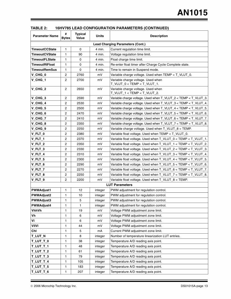
Lead Charging Parameters (Cont.)
TimeoutCCState 1 0 4 min. Current regulation time limit.
TimeoutCVState 1 90 4 min. Voltage regulation time limit.
TimeoutFLState 1 0 4 min. Float charge time limit.
TimeoutRIFloat 1 0 4 min. Re-enter float timer after Charge Cycle Complete state.
TimeoutRemSus 1 0 4 min. Time to remain in Suspend mode.
V_CHG_0 2 2760 mV Variable charge voltage. Used when TEMP < T_VLUT_0.
V_CHG_1 2 2700 mV Variable charge voltage. Used when T_VLUT_0 < TEMP < T_VLUT_1.
V_CHG_2 2 2650 mV Variable charge voltage. Used when T_VLUT_1 < TEMP < T_VLUT_2.
V_CHG_3 2 2590 mV Variable charge voltage. Used when T_VLUT_2 < TEMP < T_VLUT_3.
V_CHG_4 2 2530 mV Variable charge voltage. Used when T_VLUT_3 < TEMP < T_VLUT_4.
V_CHG_5 2 2500 mV Variable charge voltage. Used when T_VLUT_4 < TEMP < T_VLUT_5.
V_CHG_6 2 2470 mV Variable charge voltage. Used when T_VLUT_5 < TEMP < T_VLUT_6.
V_CHG_7 2 2410 mV Variable charge voltage. Used when T_VLUT_6 < TEMP < T_VLUT_7.
V_CHG_8 2 2350 mV Variable charge voltage. Used when T_VLUT_7 < TEMP < T_VLUT_8.
V_CHG_9 2 2250 mV Variable charge voltage. Used when T_VLUT_8 < TEMP.
V_FLT_0 2 2380 mV Variable float voltage. Used when TEMP < T_VLUT_0.
V_FLT_1 2 2370 mV Variable float voltage. Used when T_VLUT_0 < TEMP < T_VLUT_1.
V_FLT_2 2 2350 mV Variable float voltage. Used when T_VLUT_1 < TEMP < T_VLUT_2.
V_FLT_3 2 2330 mV Variable float voltage. Used when T_VLUT_2 < TEMP < T_VLUT_3.
V_FLT_4 2 2310 mV Variable float voltage. Used when T_VLUT_3 < TEMP < T_VLUT_4.
V_FLT_5 2 2300 mV Variable float voltage. Used when T_VLUT_4 < TEMP < T_VLUT_5.
V_FLT_6 2 2290 mV Variable float voltage. Used when T_VLUT_5 < TEMP < T_VLUT_6.
V_FLT_7 2 2270 mV Variable float voltage. Used when T_VLUT_6 < TEMP < T_VLUT_7.
V_FLT_8 2 2250 mV Variable float voltage. Used when T_VLUT_7 < TEMP < T_VLUT_8.
V_FLT_9 2 2200 mV Variable float voltage. Used when T_VLUT_8 < TEMP.
LUT Parameters
PWMAdjust1 1 12 integer PWM adjustment for regulation control.
PWMAdjust2 1 10 integer PWM adjustment for regulation control.
PWMAdjust3 1 5 integer PWM adjustment for regulation control.
PWMAdjust4 1 1 integer PWM adjustment for regulation control.
VhhVh 1 19 mV Voltage PWM adjustment zone limit.
Vh 1 6 mV Voltage PWM adjustment zone limit.
Vl 1 6 mV Voltage PWM adjustment zone limit.
VllVl 1 44 mV Voltage PWM adjustment zone limit.
Chl 1 5 mA Current PWM adjustment zone limit.
T_LUT_N 1 8 integer Number of temperature linearization LUT entries.
T_LUT_T_0 1 38 integer Temperature A/D reading axis point.
T_LUT_T_1 1 48 integer Temperature A/D reading axis point.
T_LUT_T_2 1 61 integer Temperature A/D reading axis point.
T_LUT_T_3 1 79 integer Temperature A/D reading axis point.
T_LUT_T_4 1 105 integer Temperature A/D reading axis point.
T_LUT_T_5 1 183 integer Temperature A/D reading axis point.
T_LUT_T_6 1 207 integer Temperature A/D reading axis point.
TABLE 2: 16HV785 LEAD CONFIGURATION PARAMETERS (CONTINUED)
Parameter Name#
BytesTypical Value
Units Description
© 2006 Microchip Technology Inc. DS01015A-page 13

AN1015
LUT Parameters (Cont.)
T_LUT_M_0 2 -23362 integer Temperature linearization slope LUT entry.
T_LUT_B_0 2 1418 integer Temperature linearization Y-intercept LUT entry.
T_LUT_M_1 2 -19864 integer Temperature linearization slope LUT entry.
T_LUT_B_1 2 1352 integer Temperature linearization Y-intercept LUT entry.
T_LUT_M_2 2 -15709 integer Temperature linearization slope LUT entry.
T_LUT_B_2 2 1255 integer Temperature linearization Y-intercept LUT entry.
T_LUT_M_3 2 -12572 integer Temperature linearization slope LUT entry.
T_LUT_B_3 2 1162 integer Temperature linearization Y-intercept LUT entry.
T_LUT_M_4 2 -10206 integer Temperature linearization slope LUT entry.
T_LUT_B_4 2 1071 integer Temperature linearization Y-intercept LUT entry.
T_LUT_M_5 2 -8631 integer Temperature linearization slope LUT entry.
T_LUT_B_5 2 990 integer Temperature linearization Y-intercept LUT entry.
T_LUT_M_6 2 -10154 integer Temperature linearization slope LUT entry.
T_LUT_B_6 2 1127 integer Temperature linearization Y-intercept LUT entry.
T_LUT_M_7 2 -12875 integer Temperature linearization slope LUT entry.
T_LUT_B_7 2 1402 integer Temperature linearization Y-intercept LUT entry.
VLUT_N 1 10 integer Number of entries in V_CHG and V_FLT tables.
T_VLUT_0 1 0 coded Temperature point for V_CHG and V_FLT tables (°C * 10 + 200)/4.
T_VLUT_1 1 25 coded Temperature point for V_CHG and V_FLT tables (°C * 10 + 200)/4.
T_VLUT_2 1 50 coded Temperature point for V_CHG and V_FLT tables (°C * 10 + 200)/4.
T_VLUT_3 1 75 coded Temperature point for V_CHG and V_FLT tables (°C * 10 + 200)/4.
T_VLUT_4 1 100 coded Temperature point for V_CHG and V_FLT tables (°C * 10 + 200)/4.
T_VLUT_5 1 112 coded Temperature point for V_CHG and V_FLT tables (°C * 10 + 200)/4.
T_VLUT_6 1 125 coded Temperature point for V_CHG and V_FLT tables (°C * 10 + 200)/4.
T_VLUT_7 1 150 coded Temperature point for V_CHG and V_FLT tables (°C * 10 + 200)/4.
T_VLUT_8 1 175 coded Temperature point for V_CHG and V_FLT tables (°C * 10 + 200)/4.
LED Parameters
LED1State1 1 00000000b binary LED1 display during state 1: Charge Pending.
LED1State2 1 00000000b binary LED1 display during state 2: Charge Qualification.
LED1State3 1 00000000b binary LED1 display during state 3: Current Regulation.
LED1State4 1 00000000b binary LED1 display during state 4: Voltage Regulation.
LED1State5 1 00000000b binary LED1 display during state 5: Float Charge.
LED1State6 1 00000000b binary LED1 display during state 6: Charge Cycle Complete.
LED1State7 1 00000000b binary LED1 display during state 7: Charge Suspend.
LED1State8 1 00000000b binary LED1 display during state 8: Unused.
LED2State1 1 00000000b binary LED2 display during state 1: Charge Pending.
LED2State2 1 00000000b binary LED2 display during state 2: Charge Qualification.
LED2State3 1 00000000b binary LED2 display during state 3: Current Regulation.
LED2State4 1 00000000b binary LED2 display during state 4: Voltage Regulation.
LED2State5 1 00000000b binary LED2 display during state 5: Float Charge.
LED2State6 1 00000000b binary LED2 display during state 6: Charge Cycle Complete.
LED2State7 1 00000000b binary LED2 display during state 7: Charge Suspend.
LED2State8 1 00000000b binary LED2 display during state 8: Unused.
TABLE 2: 16HV785 LEAD CONFIGURATION PARAMETERS (CONTINUED)
Parameter Name#
BytesTypical Value
Units Description
DS01015A-page 14 © 2006 Microchip Technology Inc.

AN1015
FIRMWARE SUMMARY
Initialization
During initialization, the firmware will define constants,allocate resources and configure registers. Thisincludes mapping the GPIO, setting up the timers, set-ting the initial PWM frequency, outputting the optionalBATID frequency check signal, configuring the LEDpins and configuring the HVOUT pin.
Once the resources are configured, RAM is clearedand the main loop is entered.
Four of the initialization functions are described below:
1. Programming the initial PWM frequency.2. Configuring the BATID pin as an analog input
and output of the clock frequency.3. Configuring the LED2 pin as LED or
communication.4. Configuring the HVOUT pin for one of its multiple
functions.
The initial PWM frequency is configured by writing toPWMFreq, where the following table determines thePWM frequency as a function of the bits in the PWMPregister.
TABLE 3: PWM FREQUENCY
F: 8.000PWMP<6:5>
0 1 2 3
PER <4:0> 0 8000 4000 2000 1000
1 4000 2000 1000 500
2 2667 1333 667 333
3 2000 1000 500 250
4 1600 800 400 200
5 1333 667 333 167
6 1143 571 286 143
7 1000 500 250 125
8 889 444 222 111
9 800 400 200 100
10 727 364 182 91
11 667 333 167 83
12 615 308 154 77
13 571 286 143 71
14 533 267 133 67
15 500 250 125 63
16 471 235 118 59
17 444 222 111 56
18 421 211 105 53
19 400 200 100 50
20 381 190 95 48
21 364 182 91 45
22 348 174 87 43
23 333 167 83 42
24 320 160 80 40
25 308 154 77 38
26 296 148 74 37
27 286 143 71 36
28 276 138 69 34
29 267 133 67 33
30 258 129 65 32
31 250 125 63 31
© 2006 Microchip Technology Inc. DS01015A-page 15

AN1015
The BATID pin is used to determine if a battery is presentby measuring the voltage on the pin and comparing it tothe proper EEPROM parameters. Alternatively, after aReset and during initialization, this pin can be configuredby the Mode2 parameter to output a single burst of256 clocks in order to determine the frequency of theinternal oscillator.
The LED2 pin is configured as either an LED driver oras the communication pin. See the “Communication”section for more information.
The HVOUT pin is a general purpose, open-drain outputthat can be configured to report if current is flowing bythe Mode parameter.
Mode<6> = 1: Charge Current Switch
Used as an indication of charge current flowing.
HVOUT = 1: Charge current flowing
HVOUT = 0: No charge current flowing
Main Loop
The main loop cycles through the following functions:
• Performs A/D measurements• Checks measurements against triggers and
determines the charge state• Adjusts the PWM to regulate current• Operates the LEDs
• Maintains the timers• Performs EEPROM reads and writes• Performs communication transactions
The actual subroutines are:
• adc_svc: Receive the finished A/D conversions, process the data with calibration constants, etc., and store in RAM
• adc_start: Start a new set of conversions to be completed for the next cycle
• check_triggers: Compare the A/D results with parameters to determine what state the charging should be in
• chg_state_svc: Put the charger into the proper state based on A/D results
• regulate: Adjust the PWM to regulate current based on charge state and feedback measurements
• led_svc: Operate two LEDs to display the charge state
• timer_svc: Maintain the firmware timers• ee_write_buf: Background process to write the
data block in the RAM buffer into EEPROM• ccmd_svc: React to communication commands
• status_build: Build the status byte communication register
Triggers and Charge States
Once data is received from the A/D, it is compared tothe parameters using charge state formulas todetermine the proper charge states, as explained in the“Functional Description: Lead Chemistry” section.
Regulating the PWM
The PWM duty cycle is adjusted by the firmware inresponse to the charge state and the feedbackmeasurements. It is increased or decreased to keepthe voltage and current as close to the chargerequirements as possible without exceeding thoserequirements. The feedback measurements of voltageand current are compared to the required voltage andcurrent of the particular charge state the device is in.The PWM is either kept the same, increased ordecreased a little, or increased or decreased a lot as afunction of the difference between the feedbackmeasurements and the requirements.
As Table 4 shows, if the voltage feedback is no greaterthan Vh more than the requirement, and no less thanVl lower than the requirement, the PWM is unchanged.If the feedback voltage exceeds the required voltage bymore than Vl, the PWM is decreased by PWMAdjust4,etc.
Table 4 shows the PWM adjustment factors as afunction of current difference and voltage differencewhen comparing feedback to requirements:
TABLE 4: PWM ADJUSTMENT FACTORS
Current Zones
< -Cll < -Cl -Chl to +Chl > Ch > Chh
Vo
ltag
e Z
on
es > Vhh -PWMAdjust1 -PWMAdjust1 -PWMAdjust1 -PWMAdjust1 -PWMAdjust1
> Vh -PWMAdjust4 -PWMAdjust4 -PWMAdjust4 -PWMAdjust4 -PWMAdjust2
Vh to -Vl 0 0 0 -PWMAdjust4 -PWMAdjust2
< -Vl +PWMAdjust4 +PWMAdjust4 0 -PWMAdjust4 -PWMAdjust2
< -Vll +PWMAdjust3 +PWMAdjust4 0 -PWMAdjust4 -PWMAdjust2
DS01015A-page 16 © 2006 Microchip Technology Inc.

AN1015
LED Control
Two LED Configuration registers (one for each LED)determine how the LEDs are displayed when controllingon/off, flashing, flash counts and on/off times.
TABLE 5: LED CONFIGURATION REGISTERS
EEPROM parameters are used to define the settingsabove for each charge state. The LED1State1-8 andLED2State1-8 parameters are used to program theabove configuration parameters based on what statethe charger is in.
A/D Starting and Processing
The A/D operations consist of starting the A/D readingson up to 5 channels, retrieving the data and calibratingthe data.
To start the readings, the firmware programs the A/DControl registers (see the “PIC16F785 Data Sheet”(DS41249)) to perform the required measurements. Upto five channels are used for the charger function. Theyinclude the following:
• Reference Voltage
• Current• Voltage• Temperature
• BATID
When conversions are complete, flags are set so thefirmware can perform the calibration and processing.For filtering purposes, the average of 16 consecutivereadings are used for valid data.
REFERENCE VOLTAGE
The band gap reference voltage (VR) is calibrated ortranslated from the raw A/D measurement (A/DRAW) asfollows:
EQUATION 5:
Since the reference voltage is fixed, this calibration factoris used to compensate for a variance in VDD. It is used tocorrect any readings that use VDD as a reference.
CURRENT
The current reading is calibrated or translated from theraw A/D measurement (A/DRAW) as follows:
EQUATION 6:
The CurrentCF is determined by examiningEquation 6 at full scale, for example:
EQUATION 7:
Representing the decimal fraction as a ratio using apower of 2:
EQUATION 8:
Mode<7,3> Mode Description N<6:4> F<2:0>
00 OFF N/A N/A
01 Flash N + 1 Times, Pause, Repeat Flash Count = N + 1 On Time = Off Time = F + 1Pause Time = (F + 1) * 5
Max = 3
10 On N/A N/A
11 Flash Continuously On Time = N + 1 Off Time = F + 1
VR = A/DRAW * 16384/BandgapCF
BandgapCF is typically around 248 since:VR/VDD * A/DRAW(FULLSCALE) = 1212/5000 * 1023 = 248
When referenced to VR:Current = A/DRAW * CurrentCF/65536
When referenced to VDD:Current = (A/DRAW * VR/16384) * CurrentCF/65535
Current(full scale) = VREF/AMPgain/SHUNT =5000/19.6/0.100 = 2551 mA2551 = 1023 * CurrentCFCurrentCF = 2.494
CurrentCF Base = 1024CurrentCF = 2553
© 2006 Microchip Technology Inc. DS01015A-page 17
AN1015
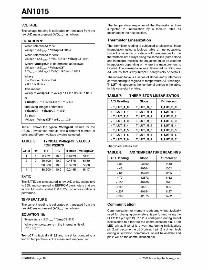
VOLTAGE
The voltage reading is calibrated or translated from theraw A/D measurement (A/DRAW) as follows:
EQUATION 9:
Table 6 shows the typical VoltageCF values for thePS2070 evaluation module with a different number ofcells and different voltage dividers selected:
TABLE 6: TYPICAL VoltageCF VALUES FOR PS2070
BATID
The BATID pin is measured in raw A/D units, scaled to 0to 255, and compared to EEPROM parameters that arein raw A/D units, scaled to 0 to 255, so no calibration isperformed.
TEMPERATUREThe current reading is calibrated or translated from theraw A/D measurement (A/DRAW) as follows:
EQUATION 10:
TempCF is typically 8192 and is set by comparing aknown temperature to the measured temperature.
The temperature response of the thermistor is thensubjected to linearization by a look-up table asdescribed in the next section.
Thermistor LinearizationThe thermistor reading is subjected to piecewise linearinterpolation using a look-up table of line equations.Since the variance of voltage with temperature for thethermistor is not always along the same line (same slopeand intercept), multiple line equations must be used forinterpolation depending on where the measurement islocated. The look-up table was developed by rating rawA/D values; that is why TempCF can typically be set to 1.
The look-up table is a series of slopes and y interceptscorresponding to regions of temperature A/D readings.T_LUT_N represents the number of entries in the table,in this case eight entries.
TABLE 7: THERMISTOR LINEARIZATION
The typical values are:
TABLE 8: A/D TEMPERATURE READINGS
Communication
Communication for memory reads and writes, typicallyused for changing parameters, is performed using theLED2 I/O pin (pin 2). Pin 2 is configured during Resetinitialization to either be the communication pin, or anLED driver. If pin 2 is driven low during initialization,pin 2 will become the LED driver. If pin 2 is driven highduring initialization, communication will be enabled andpin 2 will be the communication pin.
Cells R# R1 R2 R Ratio VoltageCF
1 1 0.232 10.0 0.9773 51212 2 10.500 10.0 0.4878 5130
3 3 20.500 10.0 0.3279 50884 4 30.900 10.0 0.2445 5117
When referenced to VR:Voltage = A/DRAW * VoltageCF/1024
When referenced to VDD:Voltage = (A/DRAW * VR/16384) * VoltageCF/1024
Where VoltageCF is determined as follows:Voltage = A/DRAW * VoltageCF’A/DRAW = (Voltage * Cells) * R/VREF * 1023
Where:R = Resistor Divider RatioVREF = 5000 mV
This means:Voltage = VoltageCF’ * Voltage * Cells * R/VREF * 1023
orVoltageCF’ = VREF/(Cells * R * 1023)
and using integer arithmetic:VoltageCF = VoltageCF’ * 1024
So that:Voltage = VoltageCF * A/DRAW /1024
Temperature = A/DRAW * TempCF/8192
Where temperature is in the internal units of: (°C + 20) * 10
A/D Reading Slope Y-intercept
< T_LUT_T_0 T_LUT_M_0 T_LUT_B_0
< T_LUT_T_1 T_LUT_M_1 T_LUT_B_1
< T_LUT_T_2 T_LUT_M_2 T_LUT_B_2
< T_LUT_T_3 T_LUT_M_3 T_LUT_B_3
< T_LUT_T_4 T_LUT_M_4 T_LUT_B_4
< T_LUT_T_5 T_LUT_M_5 T_LUT_B_5
< T_LUT_T_6 T_LUT_M_6 T_LUT_B_6
> T_LUT_T_6 T_LUT_M_7 T_LUT_B_7
A/D Reading Slope Y-intercept
< 38 -23362 1418
< 48 -19864 1352
< 61 -15709 1255
< 79 -12572 1162
< 105 -10206 1071
< 183 -8631 990
< 207 -10154 1127
> 207 -12875 1402
DS01015A-page 18 © 2006 Microchip Technology Inc.
AN1015
The communication protocol is the Single Pin Serial(SPS) protocol. SPS communication is an asynchronousreturn-to-one protocol. The signal requires an externalpull-up resistor. The timing of the driven low pulsesdefines the communication. A Break cycle starts a com-mand from the host to the 16HV785. The command iseight bits long. After this, eight data bits are either writtento the 16HV785, or read from the 16HV785.
A Break cycle is defined by a low period of time equalto or greater than time tb, then returned high for a timegreater than or equal to tbr.
The data bits consist of three sections each:
1. Start: low for at least time tstr.2. Data: data high or low valid by time tdsuh/v and
held until time tdh/v.3. Stop: high by time tssuh/v and held until time tcyc.
All transactions either read or write an 8-bit register.Each register has a 7-bit address, plus a read/write bit,for a total of 8 bits. Bit 7 is the read/write bit. When bit 7is ‘1’, the register is written. When bit 7 is ‘0’, the regis-ter is read. Of the possible 128 addressable registers,only ten are implemented.
A read transaction will receive a single byte of data. Awrite transaction can write multiple 8-bit data values toa register:
READ: BREAK, REG_ADDR, DATA.
WRITE: BREAK, REG_ADDR, DATA, DATA, ... DATA
© 2006 Microchip Technology Inc. DS01015A-page 19

AN1015
FIGURE 11: SINGLE PIN SERIAL TIMING
tB tBR
tstrh
tdsu
tdh
tssu
tcych
tstrb
tdv
tssub
tcycb
BreakCMD Address
Data to or from16HV785
LSB MSB LSB
Break 0 001001010000011
CMD Addr = 04 hex Data = 25 hex
Start bit Data bit Stop bit
Break bit Break Reset
Start bit Data bit Stop bit
Host to 16HV785
16HV785 to Host
Break Timing
CMD and DataProtocol
Communication Example
tdsub
DS01015A-page 20 © 2006 Microchip Technology Inc.
AN1015
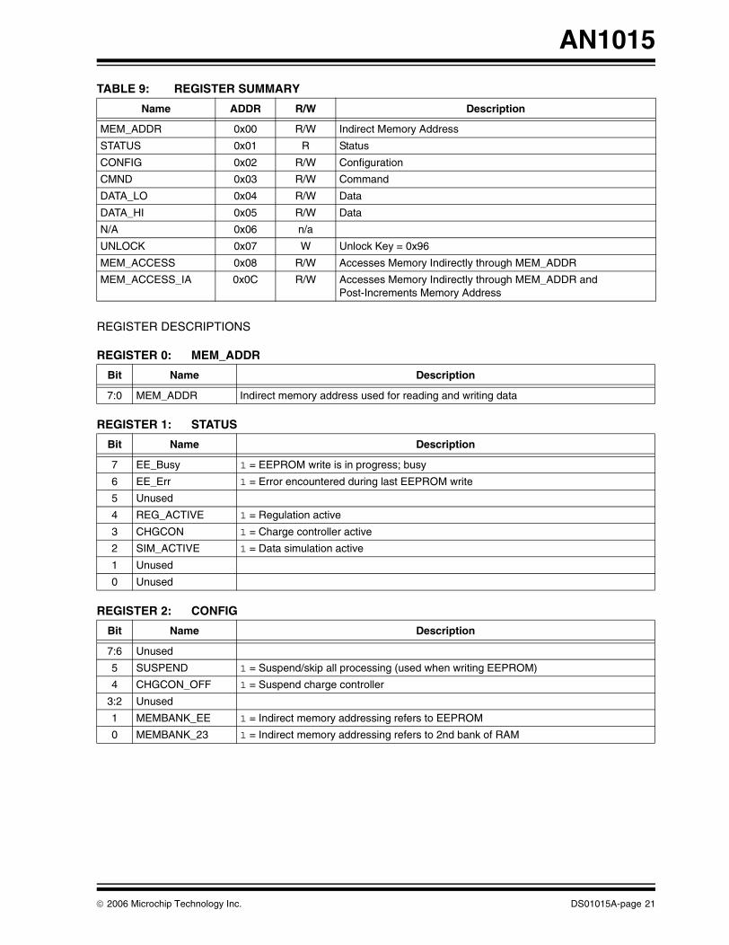
TABLE 9: REGISTER SUMMARY
REGISTER DESCRIPTIONS
REGISTER 0: MEM_ADDR
REGISTER 1: STATUS
REGISTER 2: CONFIG
Name ADDR R/W Description
MEM_ADDR 0x00 R/W Indirect Memory Address
STATUS 0x01 R Status
CONFIG 0x02 R/W Configuration
CMND 0x03 R/W Command
DATA_LO 0x04 R/W Data
DATA_HI 0x05 R/W Data
N/A 0x06 n/a
UNLOCK 0x07 W Unlock Key = 0x96
MEM_ACCESS 0x08 R/W Accesses Memory Indirectly through MEM_ADDR
MEM_ACCESS_IA 0x0C R/W Accesses Memory Indirectly through MEM_ADDR and Post-Increments Memory Address
Bit Name Description
7:0 MEM_ADDR Indirect memory address used for reading and writing data
Bit Name Description
7 EE_Busy 1 = EEPROM write is in progress; busy
6 EE_Err 1 = Error encountered during last EEPROM write
5 Unused
4 REG_ACTIVE 1 = Regulation active
3 CHGCON 1 = Charge controller active
2 SIM_ACTIVE 1 = Data simulation active
1 Unused
0 Unused
Bit Name Description
7:6 Unused
5 SUSPEND 1 = Suspend/skip all processing (used when writing EEPROM)
4 CHGCON_OFF 1 = Suspend charge controller
3:2 Unused
1 MEMBANK_EE 1 = Indirect memory addressing refers to EEPROM
0 MEMBANK_23 1 = Indirect memory addressing refers to 2nd bank of RAM
© 2006 Microchip Technology Inc. DS01015A-page 21

AN1015
REGISTER 3: CMND
REGISTER 4: DATA_LO
REGISTER 5: DATA_HI
REGISTER 6: UNUSED
REGISTER 7: UNLOCK
REGISTER 8: MEM_ACCESS
REGISTER C: MEM_ACCESS_IA
Bit Name Description
7 VERSION 1 = Load Data registers (Register 4 and Register 5) with firmware version number
6 PWM_SET 1 = Load control PWM with contents of Data registers
5 REG_ON 1 = Enable regulation module
4 EE_RQ 1 = Request EEPROM write of data block in RAM
3 Unused
2 RESET 1 = Reset firmware (branch to Reset vector from Idle loop)
1 FORCE_CHGSTATE 1 = Force branch to Charge Controller state
0 SIM_RQ 1 = Load simulation data previously written to RAM
Bit Name Description
7:0 DATA_LO Generic data used in memory reads and writes (LSB)
Bit Name Description
7:0 DATA_HI Generic data used in memory reads and writes (MSB)
Bit Name Description
7:0 Unused
Bit Name Description
7:0 UNLOCK Unlock code is written here
Bit Name Description
7:0 MEM_ACCESS Data written to Register 8 is actually sent to the memory address contained in Register 0 and the bank indicated by Register 2 (bits<1:0>)
Bit Name Description
7:0 MEM_ACCESS_IA Data written to Register 8 is actually sent to the memory address contained in Register 0 and the bank indicated by Register 2 (bits<1:0>); Register 0 will be post-incremented
DS01015A-page 22 © 2006 Microchip Technology Inc.
AN1015
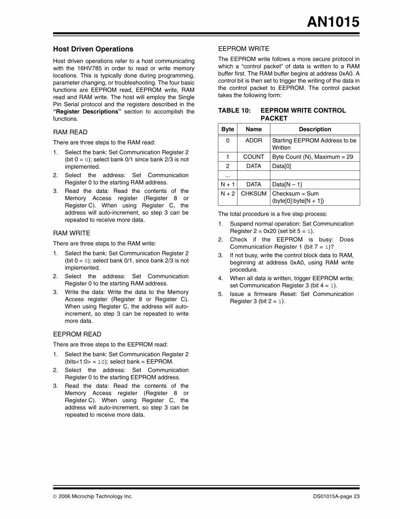
Host Driven Operations
Host driven operations refer to a host communicatingwith the 16HV785 in order to read or write memorylocations. This is typically done during programming,parameter changing, or troubleshooting. The four basicfunctions are EEPROM read, EEPROM write, RAMread and RAM write. The host will employ the SinglePin Serial protocol and the registers described in the“Register Descriptions” section to accomplish thefunctions.
RAM READ
There are three steps to the RAM read:
1. Select the bank: Set Communication Register 2(bit 0 = 0); select bank 0/1 since bank 2/3 is notimplemented.
2. Select the address: Set CommunicationRegister 0 to the starting RAM address.
3. Read the data: Read the contents of theMemory Access register (Register 8 orRegister C). When using Register C, theaddress will auto-increment, so step 3 can berepeated to receive more data.
RAM WRITE
There are three steps to the RAM write:
1. Select the bank: Set Communication Register 2(bit 0 = 0); select bank 0/1, since bank 2/3 is notimplemented.
2. Select the address: Set CommunicationRegister 0 to the starting RAM address.
3. Write the data: Write the data to the MemoryAccess register (Register 8 or Register C).When using Register C, the address will auto-increment, so step 3 can be repeated to writemore data.
EEPROM READ
There are three steps to the EEPROM read:
1. Select the bank: Set Communication Register 2(bits<1:0> = 10); select bank = EEPROM.
2. Select the address: Set CommunicationRegister 0 to the starting EEPROM address.
3. Read the data: Read the contents of theMemory Access register (Register 8 orRegister C). When using Register C, theaddress will auto-increment, so step 3 can berepeated to receive more data.
EEPROM WRITE
The EEPROM write follows a more secure protocol inwhich a “control packet” of data is written to a RAMbuffer first. The RAM buffer begins at address 0xA0. Acontrol bit is then set to trigger the writing of the data inthe control packet to EEPROM. The control packettakes the following form:
TABLE 10: EEPROM WRITE CONTROL PACKET
The total procedure is a five step process:
1. Suspend normal operation: Set CommunicationRegister 2 = 0x20 (set bit 5 = 1).
2. Check if the EEPROM is busy: DoesCommunication Register 1 (bit 7 = 1)?
3. If not busy, write the control block data to RAM,beginning at address 0xA0, using RAM writeprocedure.
4. When all data is written, trigger EEPROM write;set Communication Register 3 (bit 4 = 1).
5. Issue a firmware Reset: Set CommunicationRegister 3 (bit 2 = 1).
Byte Name Description
0 ADDR Starting EEPROM Address to be Written
1 COUNT Byte Count (N), Maximum = 29
2 DATA Data[0]
...
N + 1 DATA Data[N – 1]
N + 2 CHKSUM Checksum = Sum (byte[0]:byte[N + 1])
© 2006 Microchip Technology Inc. DS01015A-page 23

AN1015
Software License Agreement
The software supplied herewith by Microchip Technology Incorporated (the “Company”) is intended and supplied to you, theCompany’s customer, for use solely and exclusively with products manufactured by the Company.The software is owned by the Company and/or its supplier, and is protected under applicable copyright laws. All rights are reserved.Any use in violation of the foregoing restrictions may subject the user to criminal sanctions under applicable laws, as well as to civilliability for the breach of the terms and conditions of this license.THIS SOFTWARE IS PROVIDED IN AN “AS IS” CONDITION. NO WARRANTIES, WHETHER EXPRESS, IMPLIED OR STATU-TORY, INCLUDING, BUT NOT LIMITED TO, IMPLIED WARRANTIES OF MERCHANTABILITY AND FITNESS FOR A PARTICU-LAR PURPOSE APPLY TO THIS SOFTWARE. THE COMPANY SHALL NOT, IN ANY CIRCUMSTANCES, BE LIABLE FORSPECIAL, INCIDENTAL OR CONSEQUENTIAL DAMAGES, FOR ANY REASON WHATSOEVER.
FIRMWARE SOURCE CODE
Define Constants, Registers and EEPROM Locations
The following section defines variables used by thefirmware to control the charging regime. The EEPROMparameters described in the functional description areassigned addresses and variable names. Note that theinternal firmware variable names for these parametersmay not match the names used in the functional
description above. The names in the functional descrip-tion match the names in PowerTool™ 200 software.The software and data sheet names have been givennames that are more user-friendly.
The mode bits are defined which become user-select-able functions and charge features as described in thefunctional description. Variable names are defined forhardware interface registers like A/D control and data,timers, PWM configuration and GPIO.
;=====================================================================;;=====================================================================
;--- defines;#define CLOCK_4MHZ#define CLOCK_8MHZ;#define ENABLE_COMM_LOCK;#define DEBUG_ENABLE_TOGGLE
;--- firmware version#define FW_VERSION_LO 0x01#define FW_VERSION_HI 0x03
#include "p16f785.inc"
;--- configuration __CONFIG _CP_OFF & _CPD_OFF & _BOD_OFF & _BOR_OFF & _MCLRE_ON & _PWRTE_ON & _WDT_OFF & _INTRC_OSC_NOCLKOUT
;-----------------------------------------------------------;--- registers: special function ;-----------------------------------------------------------r_indf equ INDF r_tmr0 equ TMR0r_pcl equ PCLr_status equ STATUSr_fsr equ FSRr_port_a equ PORTAr_port_b equ PORTBr_port_c equ PORTCr_pclath equ PCLATH r_intcon equ INTCONr_pir1 equ PIR1r_tmr1l equ TMR1Lr_tmr1h equ TMR1Hr_t1con equ T1CONr_tmr2 equ TMR2r_t2con equ T2CONr_ccpr1l equ CCPR1L
DS01015A-page 24 © 2006 Microchip Technology Inc.

AN1015
r_ccpr1h equ CCPR1Hr_ccp1con equ CCP1CONr_wdtcon equ WDTCONr_adresh equ ADRESHr_adcon0 equ ADCON0
r_option_reg equ OPTION_REGr_tris_a equ TRISAr_tris_b equ TRISBr_tris_c equ TRISCr_pie1 equ PIE1r_pcon equ PCONr_osccon equ OSCCONr_osctune equ OSCTUNEr_ansel0 equ ANSEL0r_pr2 equ PR2r_ansel1 equ ANSEL1r_wpua equ WPUAr_ioca equ IOCAr_refcon equ REFCONr_vrcon equ VRCONr_eedata equ EEDATAr_eeadr equ EEADRr_eedata equ EEDATAr_eeadr equ EEADRr_eecon1 equ EECON1r_eecon2 equ EECON2r_adresl equ ADRESLr_adcon1 equ ADCON1r_pwmcon1 equ PWMCON1r_pwmcon0 equ PWMCON0r_pwmclk equ PWMCLKr_pwmph1 equ PWMPH1r_pwmph2 equ PWMPH2r_cm1con0 equ CM1CON0r_cm2con0 equ CM2CON0r_cm2con1 equ CM2CON1r_opa1con equ OPA1CONr_opa2con equ OPA2CON
;*** register bank limits#define ram0_start 0x20#define ram0_end 0x7f#define ram0_length ram0_end - ram0_start + 1#define ram1_start 0xa0#define ram1_end 0xef#define ram1_length ram1_end - ram1_start + 1
;-----------------------------------------------------------;--- registers: user;----------------------------------------------------------- org 0x20 ; *** bank 0r_mode res 1 ; operational mode registerr_chg_state res 1 ; charge controller "state"r_adc_0 equ $ ;r_adc_0_L res 1 ; adc result - channel 0r_adc_0_H res 1 ;r_adc_1 equ $ ;r_adc_1_L res 1 ; adc result - channel 1r_adc_1_H res 1 ;r_adc_2 equ $ ;r_adc_2_L res 1 ; adc result - channel 2r_adc_2_H res 1 ;r_adc_3 equ $ ;r_adc_3_L res 1 ; adc result - channel 3r_adc_3_H res 1 ;
© 2006 Microchip Technology Inc. DS01015A-page 25

AN1015
r_adc_4 equ $ ;r_adc_4_L res 1 ; adc result - channel 4r_adc_4_H res 1 ;r_pwm_L res 1 ; pwm settingr_pwm_H res 1 ; pwm settingr_reg_c res 2 ; regulation target: current (mA)r_reg_v res 2 ; regulation target: voltage (mV)r_comm_reg equ $ ; comm "registers" r_comm_reg_0 res 1 ; indirect address registerr_comm_reg_1 res 1 ; statusr_comm_reg_2 res 1 ; config flagsr_comm_reg_3 res 1 ; command flagsr_comm_reg_4 res 1 ; data lor_comm_reg_5 res 1 ; data hir_comm_reg_6 res 1 ;r_comm_reg_7 res 1 ;r_sim res 1 ;r_chg_timer_a res 1 ; hysteresis timerr_chg_timer_b res 1 ; hysteresis timerr_chg_timer_c res 1 ; hysteresis timerr_chg_timer_d res 1 ; hysteresis timerr_temp_1 res 1 ; location sensitive (init ram clear)r_temp_2 res 1 ; r_temp_3 res 1 ; r_temp_4 res 1 ; r_tempi_1 res 1 ; temporary reg for isrr_timer_a1 res 1 ;r_timer_b res 1 ;r_timer_b1 res 1 ;r_timer_c res 1 ;r_timer_d res 1 ;r_timer_d1 res 1 ;r_led_config_1 res 1 ;r_led_contrl_1 res 1 ;r_led_config_2 res 1 ;r_led_contrl_2 res 1 ;r_adc_control res 1 ; adc controlr_adc_raw_L res 1 ;r_adc_raw_H res 1 ;
r_count_1 res 1 ;r_accD_L res 1 ; math - accumulator - Dr_accD_H res 1 ;r_accC_L res 1 ; math - accumulator - Cr_accC_H res 1 ;r_accB_L res 1 ; math - accumulator - Br_accB_H res 1 ;r_accA_L res 1 ; math - accumulator - Ar_accA_H res 1 ;
r_comm_count res 1 ;r_comm_data res 1 ;r_comm_flags res 1 ;r_comm_data_cmnd res 1 ;
r_mode2 res 1 ;
org 0x60r_adc_accum res 2 ;r_adc_accum_count res 1 ;r_adc_avg res 2 ;r_adc_avg_shadow res 2 ;r_adc_1_ofs res 1 ;r_tcode res 1 ;;debugr_not_used res 5 ;
DS01015A-page 26 © 2006 Microchip Technology Inc.

AN1015
r_mode3 res 1 ;r_timer_d2 res 1 ;;-----------------------------------------------------------;--- registers: bank0,1,2,3 (common);----------------------------------------------------------- org 0x70 ; *** bank 0 (common area)r_shadow_1 res 1 ;r_shadow_2 res 1 ;r_shadow_3 res 1 ;;r_shadow_4 res 1 ;r_flags_1 res 1 ; assorted bit flagsr_flags_2 res 1 ; assorted bit flagsr_flags_3 res 1 ; assorted bit flagsr_flags_4 res 1 ; assorted bit flagsr_flags_5 res 1 ; assorted bit flagsr_flags_6 res 1 ; assorted bit flagsr_isr_w res 1 ; interrupt contextr_isr_status res 1 ; interrupt contextr_isr_pclath res 1 ; interrupt contextr_isr_fsr res 1 ; interrupt contextr_ee_data res 1 ; eeprom datar_ee_addr res 1 ; eeprom addressr_tempc_1 res 1 ;
#define flag0_mode_pchg_always r_mode, 7 ; always start with pchg#define flag0_mode_gpio_cutoff r_mode, 6 ; enable gpio cutoff logic#define flag0_mode_bpres_battid r_mode, 2 ; use battid for batt present#define flag0_mode_bpres_v r_mode, 1 ; battery present on voltage sense#define flag0_mode_bpres_always r_mode, 0 ; battery present - always
#define flag0_mode_cofs_dis r_mode2, 7 ; current offset - disable#define flag0_mode_oscout r_mode2, 6 ; enable oscillator out on battid#define flag0_mode_temp_k r_mode2, 5 ; use constant temperature 25degC;#define flag0_mode_nm r_mode2, 4 ; nickel metal hydride algorithm#define flag0_mode_vrchg_dis r_mode2, 2 ; voltage recharge - disable#define flag0_mode_vregco_dis r_mode2, 1 ; regulation voltage cutoff - disable#define flag0_mode_pwmas_dis r_mode2, 0 ; pwm auto shutdown - disable
#define flag0_mode_suspend_4ever r_mode3, 5 ; suspend forever#define flag0_mode_refloat r_mode3, 4 ; re-float enable#define flag0_mode_postfloat r_mode3, 3 ; float after CC,CV cycle#define flag0_mode_v_flt_k r_mode3, 2 ; use constant v float (not vlut)#define flag0_mode_v_reg_k r_mode3, 1 ; use constant v reg/charge (not vlut)#define flag0_mode_float r_mode3, 0 ; skip to float state immediately
BN_CREG_EE_BUSY equ .7 ; ee write busyBN_CREG_EE_ERR equ .6 ; error on last ee write;BN_CREG_UNLOCKED equ .5 ; comm unlockedBN_CREG_REG equ .4 ; regulation activeBN_CREG_CHGCON equ .3 ; charge controller enabledBN_CREG_SIM equ .2 ; simulation active (>=1 channel)
#define flag0_creg_st_ee_busy r_comm_reg_1, BN_CREG_EE_BUSY#define flag0_creg_st_ee_err r_comm_reg_1, BN_CREG_EE_ERR;#define flag0_creg_st_unlocked r_comm_reg_1, BN_CREG_UNLOCKED#define flag0_creg_st_reg r_comm_reg_1, BN_CREG_REG#define flag0_creg_st_chgcon r_comm_reg_1, BN_CREG_CHGCON#define flag0_creg_st_sim r_comm_reg_1, BN_CREG_SIM
#define flag0_creg_suspend r_comm_reg_2, 5#define flag0_creg_chgcon_off r_comm_reg_2, 4#define flag0_creg_membank_ee r_comm_reg_2, 1#define flag0_creg_membank_23 r_comm_reg_2, 0
© 2006 Microchip Technology Inc. DS01015A-page 27
AN1015
#define flag0_creg_version r_comm_reg_3, 7#define flag0_creg_pwm_set r_comm_reg_3, 6#define flag0_creg_reg_on r_comm_reg_3, 5#define flag0_creg_ee_rq r_comm_reg_3, 4#define flag0_creg_test r_comm_reg_3, 3#define flag0_creg_reset r_comm_reg_3, 2#define flag0_creg_fchgstate r_comm_reg_3, 1#define flag0_creg_sim_rq r_comm_reg_3, 0
#define flag_ee_busy r_flags_1, 7#define flag_ee_rq r_flags_1, 6#define flag_ee_err r_flags_1, 5#define flag_simdata_ready r_flags_1, 4#define flag_chg_state_timer r_flags_1, 3#define flag_math_temp r_flags_1, 2#define flag_timer_0 r_flags_1, 1#define flag_led_timer r_flags_1, 0
;--- trigger flags - lion;#define flag_v_le_vmin r_flags_2, 7;#define flag_v_le_vmax r_flags_2, 6;#define flag_v_le_vreg r_flags_2, 5;#define flag_v_le_vpchg r_flags_2, 4;#define flag_t_le_tmin r_flags_2, 3;#define flag_t_le_tmaxchgi r_flags_2, 2;#define flag_t_le_tmaxchg r_flags_2, 1;#define flag_t_le_tpchg r_flags_2, 0;--- trigger flags - nimh;#define flag_v_le_vpchg_nm r_flags_2, 7;#define flag_t_le_tpchg_lo_nm r_flags_2, 6;#define flag_t_le_tpchg_hi_nm r_flags_2, 5;#define flag_t_le_tmaxchg_nm r_flags_2, 4;#define flag_v_le_vmaxchg_nm r_flags_2, 3 ;#define flag_v_le_rchg_nm r_flags_2, 2;#define flag_v_le_dchg_nm r_flags_2, 1
;#define flag_unlocked r_flags_3, 7#define flag_temp_1 r_flags_3, 6#define flag_temp_2 r_flags_3, 5#define flag_neg r_flags_3, 4#define flag_chg_timer r_flags_3, 3#define flag_adcset_2_rq r_flags_3, 2#define flag_adcset_1_rq r_flags_3, 1#define flag_adcset_0_rq r_flags_3, 0
;*** WARNING: DO NOT MOVE: flag_led_2_save;*** WARNING: DO NOT MOVE: flag_led_1_save;#define flag_led_2_save r_flags_4, 7;#define flag_led_1_save r_flags_4, 6#define flag_adc_3_sim r_flags_4, 7
#define flag_adcset_2_rdy r_flags_4, 5#define flag_adcset_2_rqq r_flags_4, 4#define flag_adcset_1_rdy r_flags_4, 3#define flag_adcset_1_rqq r_flags_4, 2#define flag_adcset_0_rdy r_flags_4, 1#define flag_adcset_0_rqq r_flags_4, 0
#define flag_reg_timer r_flags_5, 7#define flag_battpres1 r_flags_5, 6#define flag_battpres r_flags_5, 5#define flag_comm_active r_flags_5, 4#define flag_reg_on r_flags_5, 3#define flag_vreg r_flags_5, 2#define flag_vreg_2 r_flags_5, 1#define flag_vreg_1 r_flags_5, 0
DS01015A-page 28 © 2006 Microchip Technology Inc.

AN1015
#define BN_CHGN_TSEL 0#define flag_chg_ti1_done r_flags_6, 7#define flag_chg_ti2_done r_flags_6, 6#define flag_chgn_tsel r_flags_6, BN_CHGN_TSEL#define MASK_CHGN_TSEL 1<<BN_CHGN_TSEL#define REG_CHGN_TSEL r_flags_6
#define ADCH_4 0x10#define ADCH_3 0x08#define ADCH_2 0x04#define ADCH_1 0x02#define ADCH_0 0x01
#define ADCSET_0 ADCH_4 | ADCH_3 | ADCH_2 | ADCH_1 | ADCH_0#define ADCSET_1 ADCH_2 | ADCH_1#define ADCSET_2 ADCH_4 | ADCH_3 | ADCH_2 | ADCH_1
#define COMM_UNLOCK_KEY 0x96
#define flag_comm_pin r_comm_flags, 5#define flag_comm_timeout r_comm_flags, 4#define flag_comm_cmnd r_comm_flags, 3#define flag_comm_bit r_comm_flags, 2#define flag_comm_H2L r_comm_flags, 1 #define flag_comm_xmit r_comm_flags, 0
;-----------------------------------------------------------;--- registers: bank1;-----------------------------------------------------------
org 0xa0 ; *** bank 1r_buf1 equ $ ; sim data, ee write buf datar_ee_buf equ $ ;r_ee_buf_adr res .1 ;r_ee_buf_cnt res .1 ;r_ee_buf_dta res .29 ;r_ee_buf_ptr res .1 ; org 0xb0r_buf2 res .16 ; overlaps 2nd half of r_buf1 ; scratchpad for LUT
;-----------------------------------------------------------;--- registers: bank2;----------------------------------------------------------- org 0x110 ; *** bank 2
;-----------------------------------------------------------;--- registers: bank3;----------------------------------------------------------- org 0x190 ; *** bank 3
;-----------------------------------------------------------;--- constants: timing;-----------------------------------------------------------
;=== option reg#ifdef CLOCK_8MHZclk_p equ .8000000 ; (mhz) clock frequencyOSCCON_DEFAULT equ 0x70 ;
;--- optionoption_default equ 1<<NOT_RAPU | 0x02
© 2006 Microchip Technology Inc. DS01015A-page 29

AN1015
tmr1_default equ 0x10 ; 2:1 scale, 1usec ticTIME_COMM_USEC_T equ 1#endif
clk_i equ clk_p / .4 ; (mhz) instruction clock timer resolution (class b)
TIMER_A_USEC equ .1024 ; (usec) timer resolution (class a)TIMER_B_MSEC equ .250 ; (msec) timer resolution (class b)TIMER_C_MSEC equ .1000 ; (msec) timer resolution (class c);debug;TIMER_D_SEC equ .15 ; (sec) timer resolution (class d)TIMER_D_SEC equ .240 ; (sec) timer resolution (class d);debug;TIMER_A1_MSEC equ .2 ; (msec) regulation timer TIMER_A1_MSEC equ .20 ; (msec) regulation timer
TIMER_A1_TA equ ((TIMER_A1_MSEC * .1000) + TIMER_A_USEC / 2) / TIMER_A_USECTIMER_B_TA equ (TIMER_B_MSEC * .1000) / TIMER_A_USECTIMER_C_TB equ (TIMER_C_MSEC) / TIMER_B_MSECTIMER_D_TC equ (TIMER_D_SEC * .1000) / TIMER_C_MSEC
TIME_COMM_REPLY_USEC equ .250TIME_COMM_B1_LO_USEC equ .20TIME_COMM_B1_HI_USEC equ .230TIME_COMM_B0_LO_USEC equ .170TIME_COMM_B0_HI_USEC equ .080
TIME_COMM_0_MAX_USEC equ .175TIME_COMM_1_MAX_USEC equ .70TIME_COMM_BREAK_USEC equ .200
TIME_COMM_REPLY_T equ TIME_COMM_REPLY_USEC / TIME_COMM_USEC_TTIME_COMM_B1_LO_T equ TIME_COMM_B1_LO_USEC / TIME_COMM_USEC_TTIME_COMM_B0_LO_T equ TIME_COMM_B0_LO_USEC / TIME_COMM_USEC_TTIME_COMM_B1_HI_T equ TIME_COMM_B1_HI_USEC / TIME_COMM_USEC_TTIME_COMM_B0_HI_T equ TIME_COMM_B0_HI_USEC / TIME_COMM_USEC_TTIME_COMM_0_MAX_T equ TIME_COMM_0_MAX_USEC / TIME_COMM_USEC_TTIME_COMM_1_MAX_T equ TIME_COMM_1_MAX_USEC / TIME_COMM_USEC_TTIME_COMM_BREAK_T equ TIME_COMM_BREAK_USEC / TIME_COMM_USEC_T
;-----------------------------------------------------------;--- constants: i/o configuration;-----------------------------------------------------------#define TRIS_A_COMM b'11111011'#define TRIS_B_DEFAULT b'00111111'#define TRIS_C_BIOUT b'11001101'#define TRIS_C_DEFAULT b'11001111'
#define p_led_1 r_port_b, 7#define p_gpio r_port_b, 6#define p_led_2 r_port_a, 5#define p_comm r_port_a, 5#define p_batid r_port_c, 1
;--- IOCA#define IOCA_DEFAULT 1<<IOCA5
;--- WPUA#define WPUA_DEFAULT 1<<WPUA5
;--- OPA1CON;debug OVP#define OPA1CON_DEFAULT 1<<OPAON;#define OPA1CON_DEFAULT 0<<OPAON
DS01015A-page 30 © 2006 Microchip Technology Inc.

AN1015
;--- OPA2CON#define OPA2CON_DEFAULT 1<<OPAON
;--- CM1: INPUTS: RA1/C1Ref SPEED: NORM, OUTPUT: INT;#define CM1CON0_DEFAULT 1<<C1R | 1<<C1SP | 1<<C1ON;debug OVP#define CM1CON0_DEFAULT 1<<C1R | 1<<C1SP | 1<<C1ON | 1<<C1OE
;--- CM2: INPUTS: RC3/AN4 SPEED: NORM, OUTPUT: INT#define CM2CON0_DEFAULT 1<<C2ON | 0<<C2POL | .0<<C2SP | 0<<C2R | .3<<C2CH0 #define CM2CON1_DEFAULT 0
;--- VRCON: default 1.2V#define VRCON_DEFAULT 0
;--- REFCON: ENABLED#define REFCON_DEFAULT 1<<VREN | 0<<VROE
;--- ANSEL0#define ANSEL0_DEFAULT 1<<ANS0 | 1<<ANS1 | 0<<ANS2 | 1<<ANS3 | 1<<ANS4 | 0<<ANS5
;--- ANSEL1#define ANSEL1_DEFAULT 1<<ANS8 | 1<<ANS9 | 1<<ANS10 | 1<<ANS11
;--- PWMCON0#define PWMCON0_AS_DIS 0<<BLANK2 | 1<<PH2EN#define PWMCON0_AS_EN 0<<BLANK2 | 1<<PH2EN | 1<<PASEN
;--- PWMCLK#define PWMCLK_DEFAULT .0<<PWMP0 | .19<<PER0
;--- PWMPH2#define PWMPH2_DEFAULT 0<<POL | 1<<C2EN | 0<<C1EN | .1<<PH0
;--- ADCON#define ADC_ADCON0_DEFAULT 1<<ADFM | 1<<ADON
#define ADC_ADCON0_0 ADC_ADCON0_DEFAULT | .13<<CHS0 | 0<<VCFG #define ADC_ADCON0_1 ADC_ADCON0_DEFAULT | .06<<CHS0 | 0<<VCFG#define ADC_ADCON0_2 ADC_ADCON0_DEFAULT | .03<<CHS0 | 0<<VCFG#define ADC_ADCON0_3 ADC_ADCON0_DEFAULT | .00<<CHS0 | 0<<VCFG#define ADC_ADCON0_4 ADC_ADCON0_DEFAULT | .05<<CHS0 | 0<<VCFG#define ADC_CHANNEL_MASK 0x1F
#define ADC_ADCON1_DEFAULT 0x05<<ADCS0
;--- ADC_TAQ (# of 3-instruction loops ... 8mhz => 1.5us/loop); .83 => 125usec .21 => 32usec ;debug#define ADC_TAQ .51
;--- CCP1CON#define CCP1CON_DEFAULT 0x0c
;-----------------------------------------------------------;--- constants: interrupts;-----------------------------------------------------------#define INTCON_DEFAULT 1<<T0IE
;-----------------------------------------------------------;--- constants: ;-----------------------------------------------------------PWM_DEFAULT equ .000
;-----------------------------------------------------------
© 2006 Microchip Technology Inc. DS01015A-page 31

AN1015
;--- EE MAP;-----------------------------------------------------------EE_PATTERN equ .0EE_NCELLS equ .2EE_CAPACITY equ .19EE_PWM_FREQ equ .21EE_MODE equ .22EE_MODE2 equ .23EE_OSC_TRIM equ .24
EE_LED1_CFG equ .32EE_LED2_CFG equ .40
EE_REG_P1 equ .52EE_REG_P2 equ .53EE_REG_P3 equ .54EE_REG_P4 equ .55EE_REG_VHH_VH equ .56EE_REG_VH equ .57EE_REG_VL equ .58EE_REG_VLL_VL equ .59EE_REG_CNULL equ .60EE_REG_VSAFETY equ .61
EE_CHG_C equ .67EE_CHG_C_FLOAT equ .69EE_CHG_C_MIN equ .71EE_CHG_TI_CC equ .73EE_CHG_TI_CV equ .74EE_CHG_TI_FLOAT equ .75EE_CHG_TI_REFLOAT equ .76EE_CHG_TI_SUSPEND equ .77EE_CHG_V_CHG_K equ .78EE_CHG_V_FLT_K equ .80EE_CHG_V_MIN_BP equ .82
EE_CHG_TIME_0 equ .92EE_CHG_TIME_1 equ .93EE_CHG_TIME_2 equ .94EE_CHG_TIME_3 equ .95EE_CHG_TIME_4 equ .96EE_CHG_TIME_5 equ .97EE_BATTID_MIN equ .98EE_BATTID_MAX equ .99
EE_CAL_ADC equ .108EE_CAL_ADC_0 equ .108EE_CAL_ADC_1 equ .110EE_CAL_ADC_2 equ .112EE_CAL_ADC_3 equ .114EE_CAL_ADC_4 equ .116EE_SHUNT equ .118EE_T_DEFAULT equ .119
EE_T_LUT_N equ .124EE_T_LUT_T equ .125EE_T_LUT_MB equ .132
EE_MODE3 equ .170EE_VLUT_N equ .171EE_VLUT_T equ .172EE_VLUT_CHG equ .181EE_VLUT_FLT equ .201
;=====================================================================
DS01015A-page 32 © 2006 Microchip Technology Inc.

AN1015
Interrupt Service
This routine sets up the Reset vector, then the InterruptStatus register for “PORTA” GPIO, and the interruptand communication timers.
org 0x00vector_reset: ; goto start ;
org 0x0004 ;isr: ;vector_isr: ; movwf r_isr_w ; save context swapf r_status, w ; clrf r_status ; movwf r_isr_status ; movf r_pclath, w ; movwf r_isr_pclath ; movf r_fsr, w ; movwf r_isr_fsr ;
isr_rac: ; isr: PORTA CHANGE btfss r_intcon, RAIF ; goto isr_rbc_x ; movf r_port_a, w ; bcf flag_comm_pin ; btfsc r_port_a, 5 ; bsf flag_comm_pin ; bcf r_intcon, RAIF ;; incf r_temp_3, f ; call comm_isr ;; call blink_3 ;isr_rbc_x: ;
isr_t1: ; isr: TMR1 btfss r_pir1, TMR1IF ; goto isr_t1_x ; bcf r_pir1, TMR1IF ; bcf r_t1con, TMR1ON ; bsf flag_comm_timeout ; call comm_isr ;isr_t1_x: ;
isr_t0: ; isr: TMR0 btfss r_intcon, T0IF ; goto isr_t0_x ; bcf r_intcon, T0IF ; bsf flag_timer_0 ;isr_t0_x: ;
isr_x: ; movf r_isr_fsr, w ; movwf r_fsr ; movf r_isr_pclath, w ; movwf r_pclath ; swapf r_isr_status, w ; movwf r_status ; swapf r_isr_w, f ; swapf r_isr_w, w ;
retfie ;;=====================================================================
© 2006 Microchip Technology Inc. DS01015A-page 33

AN1015
;debug#ifdef DEBUG_ENABLE_TOGGLE#define p_toggle r_port_c, 1
blink_4: bsf r_port_c, 1 ; bcf r_port_c, 1 ;blink_3: bsf r_port_c, 1 ; bcf r_port_c, 1 ;blink_2: bsf r_port_c, 1 ; bcf r_port_c, 1 ;blink_1: bsf r_port_c, 1 ; bcf r_port_c, 1 ; return ;toggle: btfss flag_temp_1 ; goto toggle_1 ; bcf flag_temp_1 ; bcf r_port_c, 1 ; return ;toggle_1: bsf flag_temp_1 ; bsf r_port_c, 1 ; return ;#endif
DS01015A-page 34 © 2006 Microchip Technology Inc.
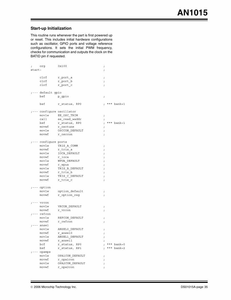
AN1015
Start-up Initialization
This routine runs whenever the part is first powered upor reset. This includes initial hardware configurationssuch as oscillator, GPIO ports and voltage referenceconfigurations. It sets the initial PWM frequency,checks for communication and outputs the clock on theBATID pin if requested.
; org 0x100 ;start: ;
clrf r_port_a ; clrf r_port_b ; clrf r_port_c ;
;--- default gpio bsf p_gpio ;
bsf r_status, RP0 ; *** bank=1
;--- configure oscillator movlw EE_OSC_TRIM ; call ee_read_waddr ; bsf r_status, RP0 ; *** bank=1 movwf r_osctune ; movlw OSCCON_DEFAULT ; movwf r_osccon ;
;--- configure ports movlw TRIS_A_COMM ; movwf r_tris_a ; movlw IOCA_DEFAULT ; movwf r_ioca ; movlw WPUA_DEFAULT ; movwf r_wpua ; movlw TRIS_B_DEFAULT ; movwf r_tris_b ; movlw TRIS_C_DEFAULT ; movwf r_tris_c ;
;--- option movlw option_default ; movwf r_option_reg ;
;--- vrcon movlw VRCON_DEFAULT ; movwf r_vrcon ;;--- refcon movlw REFCON_DEFAULT ; movwf r_refcon ;;--- ansel movlw ANSEL0_DEFAULT ; movwf r_ansel0 ; movlw ANSEL1_DEFAULT ; movwf r_ansel1 ; bcf r_status, RP0 ; *** bank=0 bsf r_status, RP1 ; *** bank=2;--- opamps movlw OPA1CON_DEFAULT ; movwf r_opa1con ; movlw OPA2CON_DEFAULT ; movwf r_opa2con ;
© 2006 Microchip Technology Inc. DS01015A-page 35

AN1015
;--- comparators movlw CM1CON0_DEFAULT ; movwf r_cm1con0 ; movlw CM2CON0_DEFAULT ; movwf r_cm2con0 ; movlw CM2CON1_DEFAULT ; movwf r_cm2con1 ;
bcf r_status, RP1 ; *** bank=0
bsf r_t1con, TMR1ON ; enable timer 1
;--- clear ram bcf r_status, IRP ; movlw 0x20 ; movwf r_fsr ; movlw .96 ; call ram_clear ; movlw 0xA0 ; movwf r_fsr ; movlw .32 ; call ram_clear ;
;--- setup timer(s) movlw tmr1_default ; movwf r_t1con ; ;--- move MODE params from ee movlw EE_MODE ; call ee_read_waddr_ia ; movwf r_mode ; call ee_read ; movwf r_mode2 ; movlw EE_MODE3 ; call ee_read_waddr ; movwf r_mode3 ;
;--- pwm movlw EE_PWM_FREQ ; call ee_read_waddr ; andlw 0x7f ; bsf r_status, RP1 ; *** bank=2 movwf r_pwmclk ; movlw PWMPH2_DEFAULT ; movwf r_pwmph2 ; bcf r_status, RP1 ; *** bank=0 movlw PWMCON0_AS_DIS ; btfss flag0_mode_pwmas_dis ; movlw PWMCON0_AS_EN ; bsf r_status, RP1 ; *** bank=2 movwf r_pwmcon0 ; bcf r_status, RP1 ; *** bank=0 ;--- config pwm call pwm_config ;
init: ;;---------------------------------------main_init: ;
;--- init chg controller timer movlw 0xff ; movwf r_chg_timer_a ;
DS01015A-page 36 © 2006 Microchip Technology Inc.
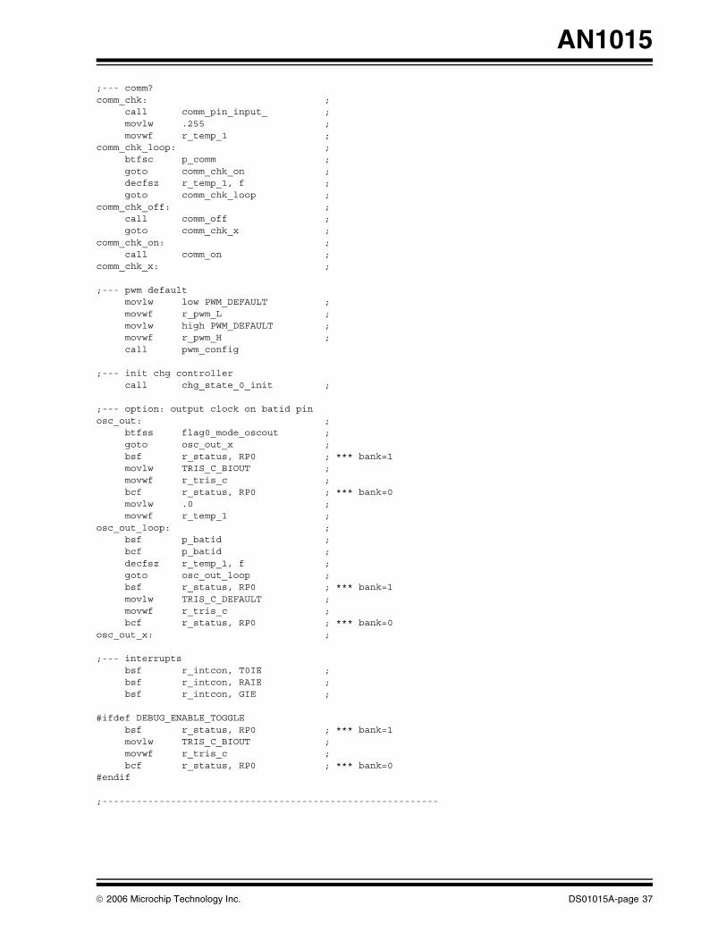
AN1015
;--- comm?comm_chk: ; call comm_pin_input_ ; movlw .255 ; movwf r_temp_1 ;comm_chk_loop: ; btfsc p_comm ; goto comm_chk_on ; decfsz r_temp_1, f ; goto comm_chk_loop ;comm_chk_off: ; call comm_off ; goto comm_chk_x ;comm_chk_on: ; call comm_on ;comm_chk_x: ;
;--- pwm default movlw low PWM_DEFAULT ; movwf r_pwm_L ; movlw high PWM_DEFAULT ; movwf r_pwm_H ; call pwm_config
;--- init chg controller call chg_state_0_init ;
;--- option: output clock on batid pinosc_out: ; btfss flag0_mode_oscout ; goto osc_out_x ; bsf r_status, RP0 ; *** bank=1 movlw TRIS_C_BIOUT ; movwf r_tris_c ; bcf r_status, RP0 ; *** bank=0 movlw .0 ; movwf r_temp_1 ;osc_out_loop: ; bsf p_batid ; bcf p_batid ; decfsz r_temp_1, f ; goto osc_out_loop ; bsf r_status, RP0 ; *** bank=1 movlw TRIS_C_DEFAULT ; movwf r_tris_c ; bcf r_status, RP0 ; *** bank=0 osc_out_x: ;
;--- interrupts bsf r_intcon, T0IE ; bsf r_intcon, RAIE ; bsf r_intcon, GIE ;
#ifdef DEBUG_ENABLE_TOGGLE bsf r_status, RP0 ; *** bank=1 movlw TRIS_C_BIOUT ; movwf r_tris_c ; bcf r_status, RP0 ; *** bank=0 #endif
;-----------------------------------------------------------
© 2006 Microchip Technology Inc. DS01015A-page 37
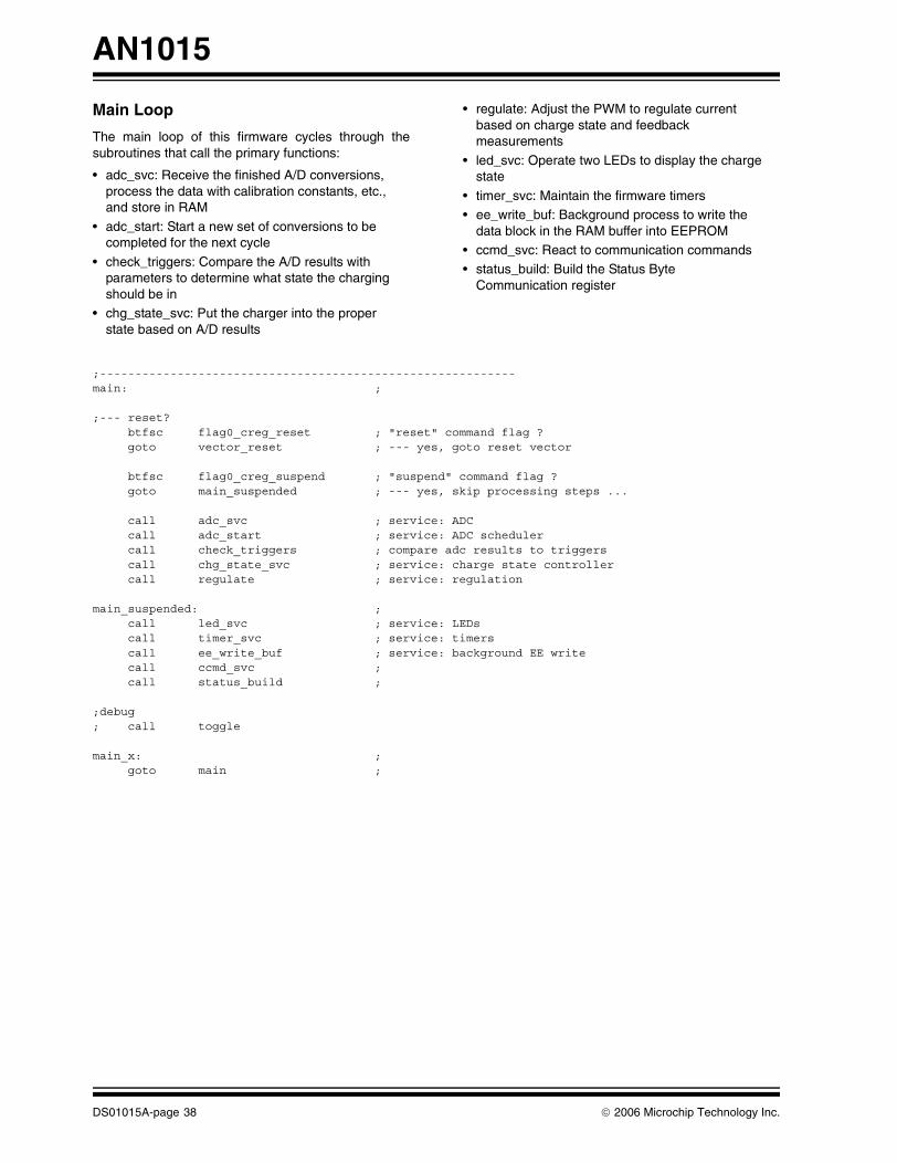
AN1015
Main Loop
The main loop of this firmware cycles through thesubroutines that call the primary functions:
• adc_svc: Receive the finished A/D conversions, process the data with calibration constants, etc., and store in RAM
• adc_start: Start a new set of conversions to be completed for the next cycle
• check_triggers: Compare the A/D results with parameters to determine what state the charging should be in
• chg_state_svc: Put the charger into the proper state based on A/D results
• regulate: Adjust the PWM to regulate current based on charge state and feedback measurements
• led_svc: Operate two LEDs to display the charge state
• timer_svc: Maintain the firmware timers• ee_write_buf: Background process to write the
data block in the RAM buffer into EEPROM• ccmd_svc: React to communication commands• status_build: Build the Status Byte
Communication register
;-----------------------------------------------------------main: ;
;--- reset? btfsc flag0_creg_reset ; "reset" command flag ? goto vector_reset ; --- yes, goto reset vector
btfsc flag0_creg_suspend ; "suspend" command flag ? goto main_suspended ; --- yes, skip processing steps ...
call adc_svc ; service: ADC call adc_start ; service: ADC scheduler call check_triggers ; compare adc results to triggers call chg_state_svc ; service: charge state controller call regulate ; service: regulation
main_suspended: ; call led_svc ; service: LEDs call timer_svc ; service: timers call ee_write_buf ; service: background EE write call ccmd_svc ; call status_build ;
;debug; call toggle
main_x: ; goto main ;
DS01015A-page 38 © 2006 Microchip Technology Inc.

AN1015
FIGURE 12: MAIN LOOP FLOWCHART
r_comm_reg_3<2> = 1?
(Firmware Reset)
r_comm_reg_2<5> = 1?
(“Suspend” mode)
call adc_svc (ADC Service)call adc_start (ADC Start)call check_triggers (Compare ADC Results to Threshold)call chg_state_svc (Service Charge Control)call regulate (Dynamic Voltage/Current Control)
call led_svc (LED Service)call timer_svc (Service Timer(s))call ee_write_buf (Execute EEPROM Control Packet)call ccmd_svc (Service Comm Control Commands)call status_build (Build Status Byte, i.e., “comm_reg_1”)
Yes
Yes
GOTOVECTOR_RESET
© 2006 Microchip Technology Inc. DS01015A-page 39

AN1015
Communication Command Service
This routine is run in response to communicationactivities that use the control bits in the Communicationregisters to modify behavior. All of the communicationfunctions as described in the functional description oncommunication are implemented below, including all of
the functionality in each bit of the Communicationregisters. Functions like reading the firmware version,setting the PWM, turning on regulation, forcing thebranch to the charge controller state machine andrunning simulation.
;---------------------------------------;--- comm command service;---------------------------------------ccmd_svc: ;
ccmd_ee_rq: ; btfss flag0_creg_ee_rq ; goto ccmd_ee_rq_x ; bcf flag0_creg_ee_rq ; bsf flag_ee_rq ;ccmd_ee_rq_x: ;
ccmd_version: ; btfss flag0_creg_version ; goto ccmd_version_x ; bcf flag0_creg_version ; movlw FW_VERSION_LO ; movwf r_comm_reg_4 ; movlw FW_VERSION_HI ; movwf r_comm_reg_5 ;ccmd_version_x: ;
ccmd_pwm_set: ; btfss flag0_creg_pwm_set ; goto ccmd_pwm_set_x ; bcf flag0_creg_pwm_set ; movf r_comm_reg_4, w ; movwf r_pwm_L ; movf r_comm_reg_5, w ; movwf r_pwm_H ; call pwm_set ;ccmd_pwm_set_x: ;
ccmd_reg_on: ; btfss flag0_creg_reg_on ; goto ccmd_reg_on_x ; bcf flag0_creg_reg_on ; call reg_on ;ccmd_reg_on_x: ;
ccmd_chg_state_force: ; btfss flag0_creg_fchgstate ; goto ccmd_chg_state_force_x ; bcf flag0_creg_fchgstate ; movf r_comm_reg_4, w ; movwf r_chg_state ; call chg_state_svc_jumptable ;ccmd_chg_state_force_x: ;
ccmd_sim_rq: ; btfss flag0_creg_sim_rq ; goto ccmd_sim_rq_x ; bcf flag0_creg_sim_rq ; call sim_rq_proc ;ccmd_sim_rq_x: ;
DS01015A-page 40 © 2006 Microchip Technology Inc.

AN1015
return ;
;-----------------------------;--- sim_rq_proc();-----------------------------sim_rq_proc: ; movlw r_buf1 ; movwf r_fsr ; bcf r_status, IRP ; movf r_indf, w ; movwf r_adc_3_L ; incf r_fsr, f ; movf r_indf, w ; movwf r_adc_3_H ; bsf flag_adc_3_sim ;sim_rq_proc_x: ; return ;
© 2006 Microchip Technology Inc. DS01015A-page 41

AN1015
Status Register Build
This routine builds the Communication Status register –Communication Register 1. This includes bitmaps forsignifying that EEPROM write is in progress, EEPROMwrite resulted in an error, regulation is active, chargecontroller is active and data simulation is active.
;---------------------------------------;--- status_build();---------------------------------------status_build: ; clrf r_temp_1 ; btfsc flag_ee_busy ; bsf r_temp_1, BN_CREG_EE_BUSY btfsc flag_ee_err ; bsf r_temp_1, BN_CREG_EE_ERR ; btfsc flag_reg_on ; bsf r_temp_1, BN_CREG_REG ; btfss flag0_creg_chgcon_off ; bsf r_temp_1, BN_CREG_CHGCON ; movlw 0x1f ; andwf r_sim, w ; btfss r_status, Z ; bsf r_temp_1, BN_CREG_SIM ; movf r_temp_1, w ; movwf r_comm_reg_1 ; return ;
DS01015A-page 42 © 2006 Microchip Technology Inc.

AN1015
PWM Configuration (Subroutine of Start-up Initialization)
This routine sets the initial PWM value during start-upinitialization.
;---------------------------------------;--- pwm_config();---------------------------------------pwm_config: ; bsf r_status, RP0 ; *** bank=1 movlw 0xff ; movwf r_pr2 ; bcf r_status, RP0 ; *** bank=0 movlw 0x80 ; movwf r_ccpr1l ; movlw 0x04 ; enable timer2 (TMR2ON) movwf r_t2con ; movlw CCP1CON_DEFAULT ; set "pwm" mode CCP1M3,2,1,0 movwf r_ccp1con ; return ;
© 2006 Microchip Technology Inc. DS01015A-page 43

AN1015
PWM Set (Subroutine of Regulate)
During the “regulate’ phase of the main loop, thisroutine is used to load the PWM in response to chang-ing PWM values. The values are typically changedbecause the charge state changed or the feedbackmeasurements are not close enough to requirements.This routine loads the PWM with the new value.
;---------------------------------------;--- pwm_set();---------------------------------------pwm_set: ; rrf r_pwm_H, w ; movwf r_accA_H ; rrf r_pwm_L, w ; movwf r_accA_L ; rrf r_accA_H, f ; rrf r_accA_L, w ; movwf r_ccpr1l ; load bits: 9:2 swapf r_pwm_L, w ; andlw 0x30 ; iorlw CCP1CON_DEFAULT ; movwf r_ccp1con ; movf r_pwm_L, w ; iorwf r_pwm_H, w ; btfsc r_status, Z ; goto pwm_disable ;pwm_enable: ; bsf r_status, RP1 ; bsf r_pwmcon0, PH2EN ; goto pwm_set_x ;pwm_disable: ; bsf r_status, RP1 ; bcf r_pwmcon0, PH2EN ;pwm_set_x: ; bcf r_status, RP1 ; return ;
DS01015A-page 44 © 2006 Microchip Technology Inc.

AN1015
PWM Adjust (Subroutine of Regulate)
This routine determines how much the PWM needs tochange as a result of feedback measurements. Thetable discussed in the functional description is followedto determine the PWM change value as a function offeedback measurements vs. requirements of voltageand current.
;---------------------------------------;--- pwm_adj();---------------------------------------pwm_adj: ; movwf r_accB_L ; accB = pwm delta clrf r_accB_H ; btfsc flag_neg ; delta negative ? call math_neg_B ; --- yes, invert ... movlw r_pwm_L ; accA = pwm call math_add_16_load_A ; accB = accA + accB = pwm + -(pwm delta) btfss r_accB_H, 7 ; result negative ? goto pwm_adj_pos ; --- no, skip ... clrf r_accB_L ; set result = 0 clrf r_accB_H ; goto pwm_adj_x ;pwm_adj_pos: ; movlw 0xfc ; result exceeds range of pwm setting ? andwf r_accB_H, w ; btfsc r_status, Z ; goto pwm_adj_x ; --- no, skip ... movlw 0x03 ; --- yes, set result = 0x03ff movwf r_accB_H ; movlw 0x0ff ; movwf r_accB_L ;pwm_adj_x: ; movlw r_pwm_L ; pwm = result call math_move_B ; return ;
© 2006 Microchip Technology Inc. DS01015A-page 45
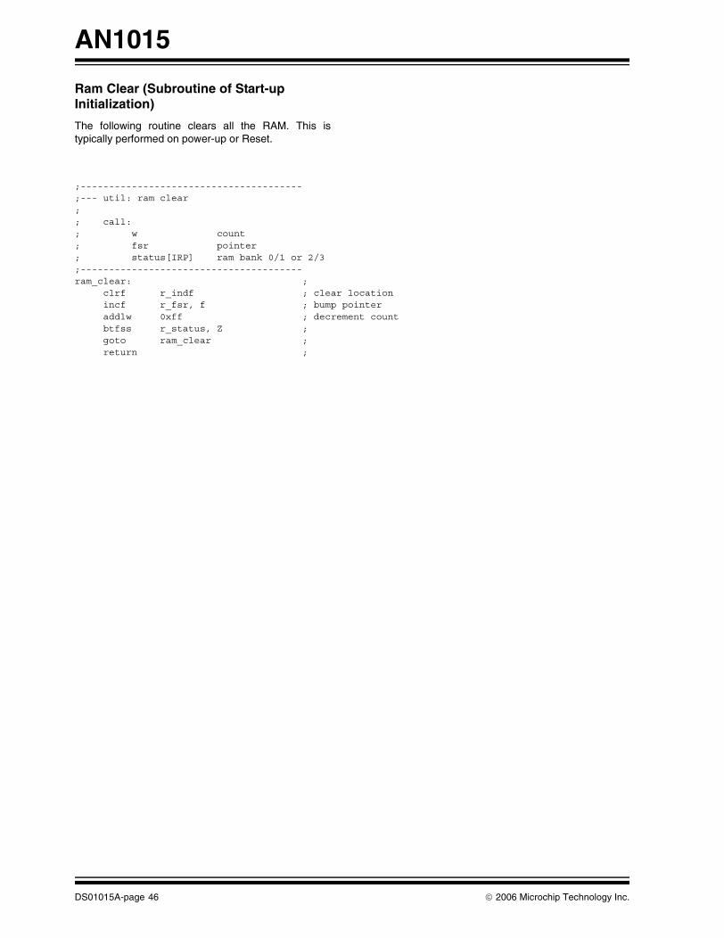
AN1015
Ram Clear (Subroutine of Start-up Initialization)
The following routine clears all the RAM. This istypically performed on power-up or Reset.
;---------------------------------------;--- util: ram clear; ; call:; w count; fsr pointer; status[IRP] ram bank 0/1 or 2/3;---------------------------------------ram_clear: ; clrf r_indf ; clear location incf r_fsr, f ; bump pointer addlw 0xff ; decrement count btfss r_status, Z ; goto ram_clear ; return ;
DS01015A-page 46 © 2006 Microchip Technology Inc.
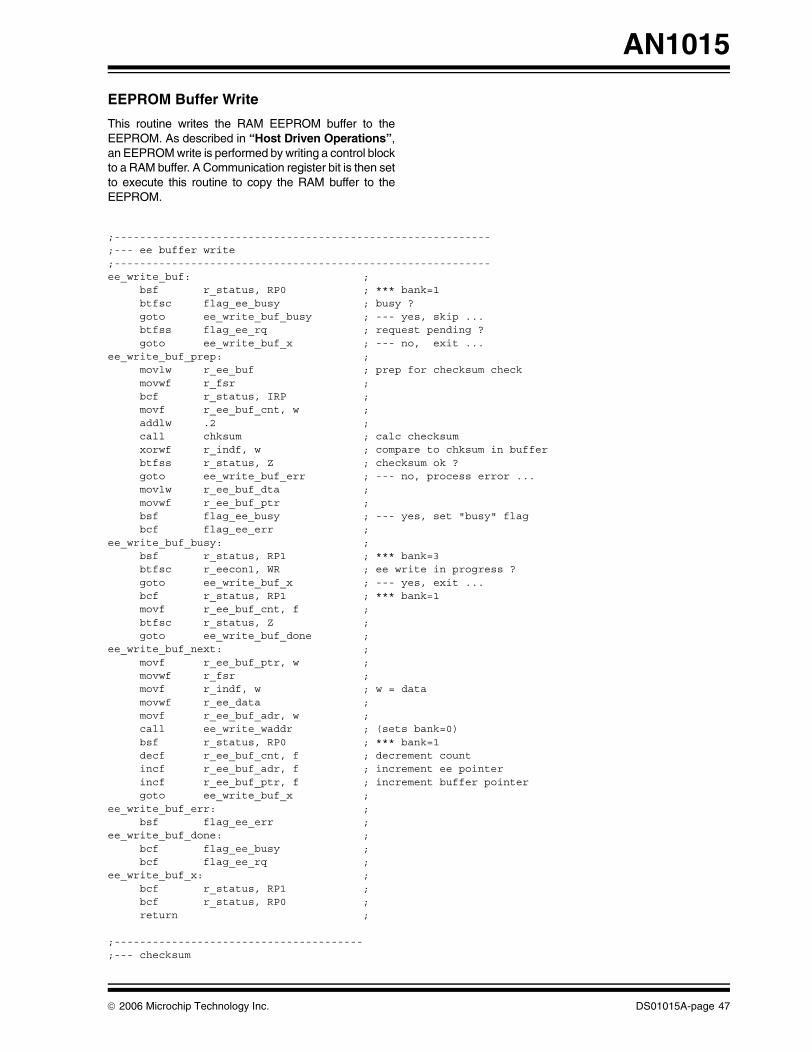
AN1015
EEPROM Buffer Write
This routine writes the RAM EEPROM buffer to theEEPROM. As described in “Host Driven Operations”,an EEPROM write is performed by writing a control blockto a RAM buffer. A Communication register bit is then setto execute this routine to copy the RAM buffer to theEEPROM.
;-----------------------------------------------------------;--- ee buffer write;-----------------------------------------------------------ee_write_buf: ; bsf r_status, RP0 ; *** bank=1 btfsc flag_ee_busy ; busy ? goto ee_write_buf_busy ; --- yes, skip ... btfss flag_ee_rq ; request pending ? goto ee_write_buf_x ; --- no, exit ...ee_write_buf_prep: ; movlw r_ee_buf ; prep for checksum check movwf r_fsr ; bcf r_status, IRP ; movf r_ee_buf_cnt, w ; addlw .2 ; call chksum ; calc checksum xorwf r_indf, w ; compare to chksum in buffer btfss r_status, Z ; checksum ok ? goto ee_write_buf_err ; --- no, process error ... movlw r_ee_buf_dta ; movwf r_ee_buf_ptr ; bsf flag_ee_busy ; --- yes, set "busy" flag bcf flag_ee_err ;ee_write_buf_busy: ; bsf r_status, RP1 ; *** bank=3 btfsc r_eecon1, WR ; ee write in progress ? goto ee_write_buf_x ; --- yes, exit ... bcf r_status, RP1 ; *** bank=1 movf r_ee_buf_cnt, f ; btfsc r_status, Z ; goto ee_write_buf_done ;ee_write_buf_next: ; movf r_ee_buf_ptr, w ; movwf r_fsr ; movf r_indf, w ; w = data movwf r_ee_data ; movf r_ee_buf_adr, w ; call ee_write_waddr ; (sets bank=0) bsf r_status, RP0 ; *** bank=1 decf r_ee_buf_cnt, f ; decrement count incf r_ee_buf_adr, f ; increment ee pointer incf r_ee_buf_ptr, f ; increment buffer pointer goto ee_write_buf_x ;ee_write_buf_err: ; bsf flag_ee_err ;ee_write_buf_done: ; bcf flag_ee_busy ; bcf flag_ee_rq ;ee_write_buf_x: ; bcf r_status, RP1 ; bcf r_status, RP0 ; return ;
;---------------------------------------;--- checksum
© 2006 Microchip Technology Inc. DS01015A-page 47
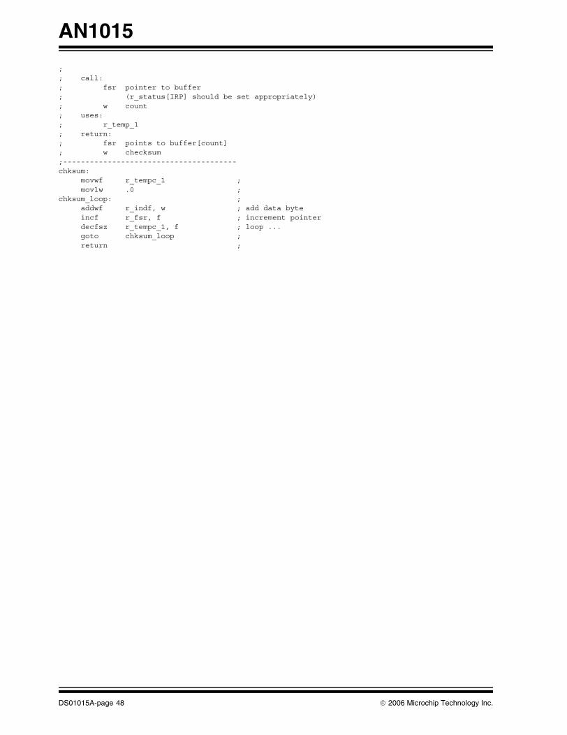
AN1015
;; call:; fsr pointer to buffer ; (r_status[IRP] should be set appropriately); w count; uses:; r_temp_1; return:; fsr points to buffer[count]; w checksum;---------------------------------------chksum: movwf r_tempc_1 ; movlw .0 ;chksum_loop: ; addwf r_indf, w ; add data byte incf r_fsr, f ; increment pointer decfsz r_tempc_1, f ; loop ... goto chksum_loop ; return ;
DS01015A-page 48 © 2006 Microchip Technology Inc.

AN1015
Thermistor Temperature Processing (Subroutine of ADC_Service)
As described in functional description, the temperaturemeasurement of the A/D converter uses a linearizationscheme composed of a look-up table of line equations.This routine uses the look-up tables to piecewiselinearly interpolate the temperature reading.
;---------------------------------------;--- thermistor temperature index; ; call:; w key;; exit:; w ram location; r_temp_3 vector length (limited); r_temp_4 key;---------------------------------------therm_index: ; movwf r_temp_4 ; save key
;--- read vector length ; movlw EE_T_LUT_N ; call ee_read_waddr ; read LUT size (N) addlw 0xff ; temperature axis length = N-1 movwf r_temp_3 ; vector length andlw 0x07 ; limit vector length
;--- setup read ee to buffer ; movwf r_temp_1 ; movlw EE_T_LUT_T ; call ee_read_buf ; read temperature vector into ram
;--- index into temperature vector ; goto lut_index_buf2 ;
;---------------------------------------;--- vlut_index() - temperature index;--- vlut_index_tcode() - temperature index w/ tcode; ; call:; w key;; exit:; w vector index; r_temp_3 vector length; r_temp_4 key;---------------------------------------vlut_index_tcode: ; movf r_tcode, w ; use 1-byte temperature as key
vlut_index: ; movwf r_temp_4 ; save key
;--- read vector length ; movlw EE_VLUT_N ; call ee_read_waddr ; read LUT size (N) addlw 0xff ; temperature axis length = N-1 movwf r_temp_3 ; vector length
;--- setup read ee to buffer ; movwf r_temp_1 ; vector length movlw EE_VLUT_T ; call ee_read_buf ; read temperature vector into ram
© 2006 Microchip Technology Inc. DS01015A-page 49
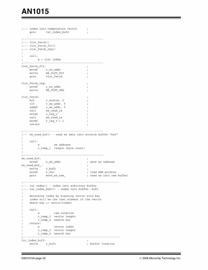
AN1015
;--- index into temperature vector ; goto lut_index_buf2 ;
;-------------------------------------------------;--- vlut_fetch();--- vlut_fetch_flt();--- vlut_fetch_chg();; call:; w = vlut index;-------------------------------------------------vlut_fetch_flt: ; movwf r_ee_addr ; movlw EE_VLUT_FLT ; goto vlut_fetch ;
vlut_fetch_chg: ; movwf r_ee_addr ; movlw EE_VLUT_CHG ;
vlut_fetch: ; bcf r_status, C ; rlf r_ee_addr, f ; addwf r_ee_addr, f ; call ee_read_ia ; movwf r_reg_v ; call ee_read_ia ; movwf r_reg_v + 1 ; return ;
;-------------------------------------------------;--- ee_read_buf() - read ee data into scratch buffer "buf";; call:; w ee address; r_temp_1 length (byte count); ;-------------------------------------------------ee_read_buf: ; movwf r_ee_addr ; save ee addressee_read_buf_: ; movlw r_buf2 ; movwf r_fsr ; load RAM pointer goto move_ee_ram_ ; read ee into ram buffer ;-----------------------------------------------------------;--- lut index() - index into arbitrary buffer;--- lut_index_buf2() - index into buffer: buf2;; determine index by scanning vector with key; index will be the last element of the vector; where key <= vector[index];; call:; w ram location; r_temp_3 vector length; r_temp_4 search key; return:; w vector index; r_temp_3 vector length; r_temp_4 search key;-----------------------------------------------------------lut_index_buf2: ; movlw r_buf2 ; buffer location
DS01015A-page 50 © 2006 Microchip Technology Inc.

AN1015
lut_index: ; movwf r_fsr ; movf r_temp_3, w ; movwf r_temp_2 ; save copy of vector lengthlut_index_loop: ; movf r_temp_4, w ; subwf r_indf, w ; btfsc r_status, C ; goto lut_index_x ; incf r_fsr, f ; decfsz r_temp_2, f ; goto lut_index_loop ;lut_index_x: ; movf r_temp_2, w ; subwf r_temp_3, w ; return ;
© 2006 Microchip Technology Inc. DS01015A-page 51

AN1015
Communication
This set of subroutines implements all the communica-tion functions: enabling or disabling communicationdepending on start-up state of the communicationGPIO, and receiving and transmitting the data.
;-----------------------------------------------------------;--- comm_on() - enable communication;-----------------------------------------------------------comm_on: ; bsf flag_comm_active ;comm_reset: ; bcf r_intcon, PEIE ; bcf r_intcon, RAIE ; clrf r_comm_flags ; goto comm_rcv_byte_prep ;
;-----------------------------------------------------------;--- comm_off() - disable communication;-----------------------------------------------------------comm_off: ; bcf r_intcon, RAIE ; bcf flag_comm_active ; call comm_pin_output_lo ; return ;
;-----------------------------------------------------------;--- comm: receive byte prep;-----------------------------------------------------------comm_rcv_byte_prep: ; call comm_pin_input ; movlw .8 ; movwf r_comm_count ; bcf flag_comm_xmit ; bsf r_intcon, RAIE ; return ;
;-----------------------------------------------------------;--- comm: timer interrupt service;-----------------------------------------------------------comm_isr: ; btfsc flag_comm_xmit ; goto comm_isr_xmit ;
comm_isr_rcv: ; btfsc flag_comm_timeout ; goto comm_reset ; break! btfsc flag_comm_pin ; goto comm_isr_rcv_1 ; bsf flag_comm_bit ; movlw TIME_COMM_BREAK_T ; call comm_timer_load ; goto comm_isr_x ;
comm_isr_rcv_1: ; btfss flag_comm_bit ; goto comm_isr_x ; call comm_timer_off ; bcf flag_comm_bit ; comf r_tmr1l, w ; sublw TIME_COMM_BREAK_T ; movwf r_tempi_1 ; sublw TIME_COMM_1_MAX_T ; btfsc r_status, C ;
DS01015A-page 52 © 2006 Microchip Technology Inc.
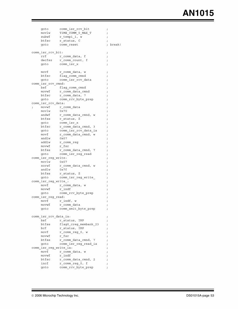
AN1015
goto comm_isr_rcv_bit ; movlw TIME_COMM_0_MAX_T ; subwf r_tempi_1, w ; btfsc r_status, C ; goto comm_reset ; break!
comm_isr_rcv_bit: ; rrf r_comm_data, f ; decfsz r_comm_count, f ; goto comm_isr_x ;
movf r_comm_data, w ; btfsc flag_comm_cmnd ; goto comm_isr_rcv_data ;comm_isr_rcv_cmnd: ; bsf flag_comm_cmnd ; movwf r_comm_data_cmnd ; btfsc r_comm_data, 7 ; goto comm_rcv_byte_prep ;comm_isr_rcv_data: ;; movwf r_comm_data ; movlw 0x70 ; andwf r_comm_data_cmnd, w ; btfss r_status, Z ; goto comm_isr_x ; btfsc r_comm_data_cmnd, 3 ; goto comm_isr_rcv_data_ia ; movf r_comm_data_cmnd, w ; andlw 0x07 ; addlw r_comm_reg ; movwf r_fsr ; btfss r_comm_data_cmnd, 7 ; goto comm_isr_reg_read ;comm_isr_reg_write: ; movlw 0x07 ; xorwf r_comm_data_cmnd, w ; andlw 0x7f ; btfss r_status, Z ; goto comm_isr_reg_write_ ;comm_isr_reg_write_: ; movf r_comm_data, w ; movwf r_indf ; goto comm_rcv_byte_prep ;comm_isr_reg_read: ; movf r_indf, w ; movwf r_comm_data ; goto comm_xmit_byte_prep ;
comm_isr_rcv_data_ia: ; bsf r_status, IRP ; btfss flag0_creg_membank_23 ; bcf r_status, IRP ; movf r_comm_reg_0, w ; movwf r_fsr ; btfss r_comm_data_cmnd, 7 ; goto comm_isr_reg_read_ia ;comm_isr_reg_write_ia: ; movf r_comm_data, w ; movwf r_indf ; btfsc r_comm_data_cmnd, 2 ; incf r_comm_reg_0, f ; goto comm_rcv_byte_prep ;
© 2006 Microchip Technology Inc. DS01015A-page 53

AN1015
comm_isr_reg_read_ia: ; btfsc flag0_creg_membank_ee ; goto comm_isr_reg_read_ee ; movf r_indf, w ; movwf r_comm_data ;comm_isr_reg_read_ia_: ; btfsc r_comm_data_cmnd, 2 ; incf r_comm_reg_0, f ; goto comm_xmit_byte_prep ;comm_isr_reg_read_ee: ; movf r_fsr, w ; call ee_read_waddr ; goto comm_isr_reg_read_ia_ ;
comm_isr_xmit: ; btfss flag_comm_H2L ; goto comm_isr_xmit_hi ;
;--- comm xmit bit - set pin locomm_isr_xmit_lo: ; call comm_pin_lo ; movlw TIME_COMM_B1_LO_T ; btfss r_comm_data, 0 ; movlw TIME_COMM_B0_LO_T ; call comm_timer_load ; bcf flag_comm_H2L ; goto comm_isr_x ;
;--- comm xmit bit - set pin hicomm_isr_xmit_hi: ; call comm_pin_hi ; decfsz r_comm_count, f ; goto $+2 ; goto comm_rcv_byte_prep ; setup for receive bsf flag_comm_H2L ; movlw TIME_COMM_B1_HI_T ; btfss r_comm_data, 0 ; movlw TIME_COMM_B0_HI_T ; call comm_timer_load ; rrf r_comm_data, f ; rotate to next bit
comm_isr_x: ; return ;
;-----------------------------------------------------------;--- comm: transmit byte prep;-----------------------------------------------------------comm_xmit_byte_prep: ; movwf r_comm_data ; load data byte movlw .8 ; movwf r_comm_count ; bsf flag_comm_xmit ; bsf flag_comm_H2L ; call comm_pin_output ; movlw TIME_COMM_REPLY_T ; call comm_timer_load ; return ;
;---------------------------------------;--- comm timer load;---------------------------------------
DS01015A-page 54 © 2006 Microchip Technology Inc.
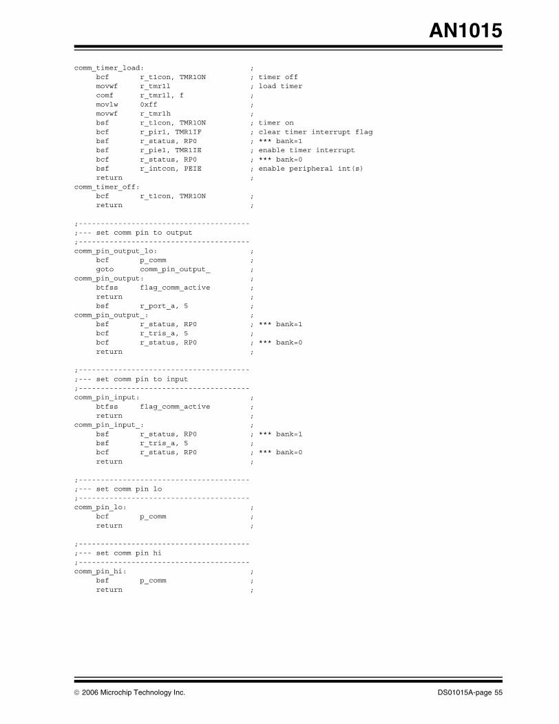
AN1015
comm_timer_load: ; bcf r_t1con, TMR1ON ; timer off movwf r_tmr1l ; load timer comf r_tmr1l, f ; movlw 0xff ; movwf r_tmr1h ; bsf r_t1con, TMR1ON ; timer on bcf r_pir1, TMR1IF ; clear timer interrupt flag bsf r_status, RP0 ; *** bank=1 bsf r_pie1, TMR1IE ; enable timer interrupt bcf r_status, RP0 ; *** bank=0 bsf r_intcon, PEIE ; enable peripheral int(s) return ;comm_timer_off: bcf r_t1con, TMR1ON ; return ;
;---------------------------------------;--- set comm pin to output;---------------------------------------comm_pin_output_lo: ; bcf p_comm ; goto comm_pin_output_ ;comm_pin_output: ; btfss flag_comm_active ; return ; bsf r_port_a, 5 ;comm_pin_output_: ; bsf r_status, RP0 ; *** bank=1 bcf r_tris_a, 5 ; bcf r_status, RP0 ; *** bank=0 return ;
;---------------------------------------;--- set comm pin to input;---------------------------------------comm_pin_input: ; btfss flag_comm_active ; return ;comm_pin_input_: ; bsf r_status, RP0 ; *** bank=1 bsf r_tris_a, 5 ; bcf r_status, RP0 ; *** bank=0 return ;
;---------------------------------------;--- set comm pin lo;---------------------------------------comm_pin_lo: ; bcf p_comm ; return ;
;---------------------------------------;--- set comm pin hi;---------------------------------------comm_pin_hi: ; bsf p_comm ; return ;
© 2006 Microchip Technology Inc. DS01015A-page 55

AN1015
LED Service
Two GPIO can be used to perform charge statefeedback with an LED display. Each LED can be pro-grammed to be on, off or flashing, and the on/off/flashtimes can be programmed using the parametersdescribed in the functional description. This routineuses the charge state and the LED configurationparameters to drive the GPIO to control the LEDproperly.
;-------------------------------------------------;--- led_init_1() - configure/initialize LED1;-------------------------------------------------led_init_1: ; movwf r_led_config_1 ; clrf r_led_contrl_1 ; bsf r_led_contrl_1, 7 ; start "off" (comment to start "on") return ;
;-------------------------------------------------;--- led_init_2() - configure/initialize LED2;-------------------------------------------------led_init_2: ; movwf r_led_config_2 ; clrf r_led_contrl_2 ; bsf r_led_contrl_2, 7 ; start "off" (comment to start "on") return ;
;-----------------------------------------------------------;--- led service;; configuration byte; [7:6] - mode; [5:3] - on time, count; [2:0] - off time; operations byte; [7:7] - led on; [6:4] - count; [3:0] - timer;-----------------------------------------------------------led_svc: ; btfss flag_led_timer ; goto led_svc_x ; bcf flag_led_timer ;
;--- led 1led_svc_1: ; movlw r_led_config_1 ; movwf r_fsr ; call led_svc_modex ; btfss r_indf, 7 ; bcf p_led_1 ; btfsc r_indf, 7 ; bsf p_led_1 ;led_svc_1_x: ;
;--- led 2led_svc_2: ; btfsc flag_comm_active ; goto led_svc_2_x ; movlw r_led_config_2 ; movwf r_fsr ; call led_svc_modex ;
DS01015A-page 56 © 2006 Microchip Technology Inc.

AN1015
btfss r_indf, 7 ; bcf p_led_2 ; btfsc r_indf, 7 ; bsf p_led_2 ;led_svc_2_x: ;
return ;
;-------------------------------------------------;--- led service: mode x;-------------------------------------------------led_svc_modex: ; btfss r_indf, 7 ; goto led_svc_modex_ ; btfss r_indf, 3 ; goto led_svc_mode2 ; goto led_svc_mode3 ;led_svc_modex_: ; btfsc r_indf, 3 ; goto led_svc_mode1 ; incf r_fsr, f ;
;---------------------------------------;--- led service: mode 0;---------------------------------------led_svc_mode0: ; incf r_fsr, f ; bcf r_indf, 7 ; goto led_svc_x ;
;---------------------------------------;--- led service: mode 1;---------------------------------------led_svc_mode1: ; incf r_fsr,f ; timer==0 ? movlw 0x0f ; andwf r_indf, w ; btfss r_status, Z ; goto led_svc_dec_x ; --- no, decrement & exit ... btfss r_indf, 7 ; led currently on ? goto led_svc_mode1_off ; --- no, jump ...
led_svc_mode1_on: ; movf r_indf, w ; andlw 0x70 ; btfss r_status, Z ; goto led_svc_mode3_on ; blink count<>0, go load timer ...
clrf r_indf ; load long "off" time decf r_fsr, f ; movf r_indf, w ; andlw 0x07 ; incf r_fsr, f ; movwf r_indf ; incf r_indf, f ; bcf r_status, C ; rlf r_indf, f ; bcf r_status, C ; rlf r_indf, f ; addwf r_indf, f ; movlw 0xf0 ; andwf r_indf, w ; movlw 0x0f ; btfss r_status, Z ; movwf r_indf ;
© 2006 Microchip Technology Inc. DS01015A-page 57

AN1015
goto led_svc_x ;
led_svc_mode1_off: ; bsf r_indf, 7 ; movf r_indf, w ; andlw 0x70 ; btfss r_status, Z ; goto led_svc_mode1_off_ ; blink count<>0, decrement & go ... decf r_fsr, f ; re-load blink count movf r_indf, w ; andlw 0x70 ; incf r_fsr, f ; iorwf r_indf, f ; goto led_svc_mode3_on_ ;
led_svc_mode1_off_: ; movlw 0x10 ; subwf r_indf, f ; goto led_svc_mode3_on_ ;
;---------------------------------------;--- led service: mode 2;---------------------------------------led_svc_mode2: ; incf r_fsr, f ; bsf r_indf, 7 ; goto led_svc_x ;
;---------------------------------------;--- led svc mode: 3 ;---------------------------------------led_svc_mode3: ; incf r_fsr,f ; count==0 ? movlw 0x0f ; andwf r_indf, w ; btfss r_status, Z ; goto led_svc_dec_x ; --- no, decrement on exit ... btfss r_indf, 7 ; led currently on ? goto led_svc_mode3_off ; --- no, jump ...led_svc_mode3_on: ; bcf r_indf, 7 ;led_svc_mode3_on_: ; decf r_fsr, f ; movf r_indf, w ; goto led_svc_mode3_ ;led_svc_mode3_off: ; bsf r_indf, 7 ; decf r_fsr, f ; point to config register swapf r_indf, w ; led_svc_mode3_: ; andlw 0x07 ; incf r_fsr, f ; iorwf r_indf, f ; goto led_svc_x ;led_svc_dec_x: ; decf r_indf, f ;
;---led_svc_x: ; return ;
DS01015A-page 58 © 2006 Microchip Technology Inc.

AN1015
Timer Service
This routine maintains the timers that are used forvarious firmware purposes, including charge controllimits.
;-----------------------------------------------------------;--- timer service;-----------------------------------------------------------timer_svc: ; btfss flag_timer_0 ; goto timer_svc_x ; bcf flag_timer_0 ;
;--- class "a" timertimer_svc_a1: ; incf r_timer_a1, f ; movlw TIMER_A1_TA ; subwf r_timer_a1, w ; btfss r_status, C ; goto timer_svc_a1_x ; clrf r_timer_a1 ; bsf flag_reg_timer ;timer_svc_a1_x: ;
;--- class "b" timer incf r_timer_b, f ; movlw TIMER_B_TA ; subwf r_timer_b, w ; btfss r_status, C ; goto timer_svc_x ; clrf r_timer_b ; bsf flag_led_timer ; bsf flag_chg_state_timer ;; decf r_timer_b1, f ;
;--- class "c" timer incf r_timer_c, f ; movlw TIMER_C_TB ; subwf r_timer_c, w ; btfss r_status, C ; goto timer_svc_x ; clrf r_timer_c ;
;--- class "d" timer incf r_timer_d, f ; movlw TIMER_D_TC ; subwf r_timer_d, w ; btfss r_status, C ; goto timer_svc_x ; clrf r_timer_d ;
timer_svc_d1: ; movf r_timer_d1, f ; btfsc r_status, Z ; goto timer_svc_d1_x ; decf r_timer_d1, f ; btfsc r_status, Z ; bsf flag_chg_ti1_done ;timer_svc_d1_x: ;
© 2006 Microchip Technology Inc. DS01015A-page 59
AN1015
timer_svc_d2: ; movf r_timer_d2, f ; btfsc r_status, Z ; goto timer_svc_d2_x ; decf r_timer_d2, f ; btfsc r_status, Z ; bsf flag_chg_ti2_done ;timer_svc_d2_x: ;
timer_svc_x: ;
return ;
DS01015A-page 60 © 2006 Microchip Technology Inc.

AN1015
EEPROM Read and Write
These are general purpose routines to move databetween EEPROM and RAM.
;-----------------------------------------------------------;--- move_ee_ram() - move data from eeprom to ram;; call:; r_fsr ram address; r_ee_addr eeprom address; w byte count; uses:; r_temp_1; return:; n/a;-----------------------------------------------------------move_ee_ram: ; movwf r_temp_1 ;move_ee_ram_: ;move_ee_ram_loop: ; call ee_read_ia ; movwf r_indf ; incf r_fsr, f ; decfsz r_temp_1, f ; goto move_ee_ram_loop ; return ; ;-----------------------------------------------------------;--- eeprom read;-----------------------------------------------------------ee_read_waddr_ia: ; movwf r_ee_addr ; save addressee_read_ia: ; call ee_read ; incf r_ee_addr, f ; return ;ee_read_waddr: ; movwf r_ee_addr ; save address
ee_read: ; bcf r_status, RP1 ; *** bank=1 bsf r_status, RP0 ; movf r_ee_addr, w ; load address movwf r_eeadr ; bsf r_eecon1, RD ; movf r_eedata, w ; read data into WREG bcf r_status, RP0 ; *** bank=0 movwf r_ee_data ; return
© 2006 Microchip Technology Inc. DS01015A-page 61

AN1015
;-----------------------------------------------------------;--- eeprom write;-----------------------------------------------------------ee_write_wdata_ia: ; movwf r_ee_data ; save data call ee_write ; incf r_ee_addr, f ; return ;ee_write_waddr: ; movwf r_ee_addr ; save address
ee_write: ; bcf r_status, RP1 ; *** bank=1 bsf r_status, RP0 ; btfsc r_eecon1, WR ; wait for write in progress goto $-1 ; movf r_ee_addr, w ; movwf r_eeadr ; movf r_ee_data, w ; movwf r_eedata ; bsf r_eecon1, WREN ; bcf r_intcon, GIE ; movlw 0x55 ; movwf r_eecon2 ; movlw 0xaa ; movwf r_eecon2 ; bsf r_eecon1, WR ; bsf r_intcon, GIE ; bcf r_eecon1, WREN ; bcf r_status, RP0 ; *** bank=0 return ;
DS01015A-page 62 © 2006 Microchip Technology Inc.

AN1015
ADC Service
This routine receives the raw A/D data for voltage,current, temperature and BATID and calibrates and con-verts it to a form usable by the algorithm, as described inthe calibration section in the firmware description.
;-----------------------------------------------------------;--- adc_svc() - service adc conversion;-----------------------------------------------------------adc_svc: ; btfss r_adc_control, 7 ; conversion started ? goto adc_svc_x ; --- no, exit ... btfsc r_adcon0, GO ; conversion complete ? goto adc_svc_x ; --- no, exit ... bcf r_adc_control, 7 ; clear "conversion started" flag
;---------------------------------------;--- fetch "raw" result;--------------------------------------- bsf r_status, RP0 ; *** bank=1 movf r_adresl, w ; bcf r_status, RP0 ; *** bank=0 movwf r_adc_raw_L ; movf r_adresh, w ; movwf r_adc_raw_H ; load raw data
movlw r_adc_raw_L ; call math_load_B ; accB = raw movlw r_adc_accum ; accA = running accum call math_add_16_load_A ; accB = raw + accum movlw r_adc_accum ; call math_move_B ; move result to register: accum incf r_adc_accum_count, f ; btfss r_adc_accum_count, 4 ; accum complete ? goto adc_svc_x ; --- no, exit ...
movlw .4 ; call math_shift_BC ; accB = accum / count = avg movlw r_adc_avg ; call math_move_B ; move result to register: avg movlw r_adc_avg ; call math_load_D ; accD = result
clrf r_adc_accum_count ; reset accumlation registers clrf r_adc_accum ; clrf r_adc_accum + 1 ;
;---------------------------------------;--- process raw data;---------------------------------------adc_svc_0: ; btfss r_adc_control, 0 ; goto adc_svc_0_x ; bcf r_adc_control, 0 ;
;debug; movlw r_adc_avg_shadow ;; call math_move_D ; save result
movlw low .16384 ; movwf r_accA_L ; movlw high .16384 ; movwf r_accA_H ; call math_mul_16_prep_ ; accBC = result
© 2006 Microchip Technology Inc. DS01015A-page 63

AN1015
movlw r_accB_L ; call math_load_A ; movlw r_accC_L ; call math_load_B ; movlw EE_CAL_ADC_0 ; call ee_read_waddr_ia ; movwf r_accC_L ; call ee_read_ia ; movwf r_accC_H ; call math_div_32 ; movf r_accB_L, w ; movwf r_adc_0_L ; movf r_accB_H, w ; movwf r_adc_0_H ;adc_svc_0_x_: ; goto adc_svc_x ;adc_svc_0_x: ;
;-----------------------------;--- adc_1: current;-----------------------------adc_svc_1: ; btfss r_adc_control, 1 ; goto adc_svc_1_x ; bcf r_adc_control, 1 ;
call adc_refcal ;
;debug; movlw r_adc_avg_shadow ;; call math_move_D ; save result
movlw EE_CAL_ADC_1 ; call load_A_ee ; accA = cal factor call math_mul_16_prep_ ; accBC = result movlw .2 ; call math_shift_BC ; accB_L,accC_H = result/1024
movlw r_accC_H ; call math_load_A ; accA = result
;--- remove offset (option)adc_svc_1_cofs: ; clrf r_accB_L ; clrf r_accB_H ; btfsc flag0_mode_cofs_dis ; goto adc_svc_1_cofs_x_ ; movlw r_adc_1_ofs ; call math_load_B ; accB = -offset clrf r_accB_H ; call math_neg_B ;adc_svc_1_cofs_x_: ; call math_add_16 ; accA + accB = result - offset btfss r_accB_H, 7 ; negative ? goto adc_svc_1_cofs_x ; --- no, skip ... clrf r_accB_L ; --- yes, make zero clrf r_accB_H ;adc_svc_1_cofs_x: ;
movlw r_adc_1_L ; call math_move_B ; goto adc_svc_x ;adc_svc_1_x: ;
DS01015A-page 64 © 2006 Microchip Technology Inc.

AN1015
;-----------------------------;--- adc_2: voltage;-----------------------------adc_svc_2: ; btfss r_adc_control, 2 ; goto adc_svc_2_x ; bcf r_adc_control, 2 ;
;debug; movlw r_adc_avg_shadow ;; call math_move_D ; save result
movlw EE_CAL_ADC_2 ; call load_A_ee ; call math_mul_16_prep_ ; movlw .2 ; call math_shift_BC ; movf r_accC_H, w ; movwf r_adc_2_L ; movf r_accB_L, w ; movwf r_adc_2_H ; goto adc_svc_x ;adc_svc_2_x: ;
;-----------------------------;--- adc_3: temperature;-----------------------------adc_svc_3: ; btfss r_adc_control, 3 ; goto adc_svc_3_x ; bcf r_adc_control, 3 ;
adc_svc_3_sim: ; btfsc flag_adc_3_sim ; goto adc_svc_3_x_ ;adc_svc_3_sim_x: ;
adc_svc_3_k: ; btfss flag0_mode_temp_k ; constant temperature option goto adc_svc_3_k_x ; movlw EE_T_DEFAULT-1 ; call load_B_ee ; accB_H = temp param clrf r_accB_L ; accB_L = 0 movlw .6 ; call math_shift_BC ; accB /= 64 (i.e. param * 4) goto adc_svc_3_B ;adc_svc_3_k_x: ;
;debug; movlw r_adc_avg_shadow ;; call math_move_D ; save result
movlw EE_CAL_ADC_3 ; call load_A_ee ; call math_mul_16_prep_ ; accB,C = TSCALE = RAW * CF movlw .5 ; call math_shift_BC ; movlw r_accC_H ; call math_load_D ; accD = TSCALE' = TSCALE/8192 movlw .2 ; call math_shift_BC ; movf r_accC_H, w ; W = TSCALE' / 4 call therm_index ; W = LUT TEMPERATURE INDEX movwf r_temp_1 ; movwf r_ee_addr ; bcf r_status, C ;
© 2006 Microchip Technology Inc. DS01015A-page 65

AN1015
rlf r_ee_addr, f ; rlf r_ee_addr, f ; movlw EE_T_LUT_MB ; addwf r_ee_addr, f ; call ee_read_ia ; movwf r_accB_L ; call ee_read_ia ; movwf r_accB_H ; bcf flag_math_temp ; btfss r_accB_H, 7 ; goto $+3 ; call math_neg_B ; bsf flag_math_temp ; movf r_accB_L, w ; movwf r_accA_L ; movf r_accB_H, w ; movwf r_accA_H ; call math_mul_16_prep_ ; accB,C = TSCALE' * M movlw .5 ; call math_shift_BC ; movf r_accB_L, w ; movwf r_accB_H ; movf r_accC_H, w ; movwf r_accB_L ; accB = TSCALE' * M / 8192 btfsc flag_math_temp ; call math_neg_B ;
call ee_read_ia ; movwf r_accA_L ; call ee_read_ia ; movwf r_accA_H ; call math_add_16 ; accB = accB + yint = temperature
adc_svc_3_B: ;
adc_svc_3_under: ; btfss r_accB_H, 7 ; check limit: tcode < 0 goto adc_svc_3_under_x ; clrf r_accB_H ; clrf r_accB_L ; goto adc_svc_3_x_ ;adc_svc_3_under_x: ;
adc_svc_3_over: ; movlw 0xFC ; check limit: tcode >= 1024 andwf r_accB_H, w ; btfsc r_status, Z ; goto adc_svc_3_over_x ; movlw 0x03 ; movwf r_accB_H ; movlw 0xFF ; movwf r_accB_L ;adc_svc_3_over_x: ;
movlw r_adc_3_L ; call math_move_B ; save results
adc_svc_3_x_: ; movlw r_adc_3_L ; call math_load_B ; re-load results (needed for sim) rrf r_accB_H, f ; rrf r_accB_L, f ; rrf r_accB_H, f ; rrf r_accB_L, w ; movwf r_tcode ; goto adc_svc_x ;
DS01015A-page 66 © 2006 Microchip Technology Inc.

AN1015
adc_svc_3_x: ;
;-----------------------------;--- adc_4: battid;-----------------------------adc_svc_4: ; btfss r_adc_control, 4 ; goto adc_svc_4_x ; bcf r_adc_control, 4 ;
;debug; movlw r_adc_avg_shadow ;; call math_move_D ; save result
movlw .2 ; call math_shift_BC ; accB = result/4 (i.e. 0->255) movlw r_adc_4_L ; call math_move_B ;
bcf flag_battpres1 ; movlw EE_BATTID_MIN ; call ee_read_waddr_ia ; w = lower limit subwf r_adc_4_L, w ; btfss r_status, C ; goto adc_svc_4_x_ ; call ee_read ; w = upper limit subwf r_adc_4_L, w ; btfss r_status, C ; goto adc_svc_4_ok ; btfss r_status, Z ; goto adc_svc_4_x_ ;adc_svc_4_ok: ; bsf flag_battpres1 ;adc_svc_4_x_: ; goto adc_svc_x ;adc_svc_4_x: ; adc_svc_4_x: ; adc_svc_x: ; return ;
;----------------------------------------;--- adc_refcal(); call:; accD = adc-raw;----------------------------------------adc_refcal: ; movlw r_adc_0_L ; call math_mul_16_prep ; accBC = result movlw .6 ; call math_shift_BC ; movf r_accB_L, w ; movwf r_accD_H ; movf r_accC_H, w ; movwf r_accD_L ; accD = adc raw corrected for vref return ;
© 2006 Microchip Technology Inc. DS01015A-page 67

AN1015
ADC Start
This routine monitors the A/D status to see when a newreading should be performed, then programs the A/Dregisters to perform the correct measurements usingthe correct channels and resolutions.
;-----------------------------------------------------------;--- adc_start_reset() - reset adc scheduler;-----------------------------------------------------------adc_start_reset: ; clrf r_adc_control ; return ;
;-----------------------------------------------------------;--- adc_start() - start/initiate new coversion;-----------------------------------------------------------adc_start: ; btfsc r_adc_control, 7 ; conversion active ? goto adc_start_x ; --- yes, exit ...
;---------------------------------------;--- start conversion ;;--------------------------------------- movlw ADC_CHANNEL_MASK ; andwf r_adc_control, w ; btfsc r_status, Z ; goto adc_start_done ; bsf r_adc_control, 6 ;
btfsc r_adc_control, 4 ; movlw ADC_ADCON0_4 ; btfsc r_adc_control, 3 ; movlw ADC_ADCON0_3 ; btfsc r_adc_control, 2 ; movlw ADC_ADCON0_2 ; btfsc r_adc_control, 1 ; movlw ADC_ADCON0_1 ; btfsc r_adc_control, 0 ; movlw ADC_ADCON0_0 ;
;--- finish initializationadc_start_: ; movwf r_adcon0 ; movlw ADC_TAQ ; movwf r_temp_1 ;adc_start_loop: ; decfsz r_temp_1, f ; goto adc_start_loop ; bsf r_adcon0, GO ; bsf r_adc_control, 7 ; goto adc_start_x ;
;--- doneadc_start_done: ;
;--- set "data ready" flag(s)adc_start_done_0: ; btfss flag_adcset_0_rqq ; goto adc_start_done_0_x ; bcf flag_adcset_0_rq ; bcf flag_adcset_0_rqq ; bsf flag_adcset_0_rdy ;
DS01015A-page 68 © 2006 Microchip Technology Inc.

AN1015
adc_start_done_0_x: ;
adc_start_done_1: ; btfss flag_adcset_1_rqq ; goto adc_start_done_1_x ; bcf flag_adcset_1_rq ; bcf flag_adcset_1_rqq ; bsf flag_adcset_1_rdy ;adc_start_done_1_x: ;
adc_start_done_2: ; btfss flag_adcset_2_rqq ; goto adc_start_done_2_x ; bcf flag_adcset_2_rq ; bcf flag_adcset_2_rqq ;; bsf flag_adcset_2_rdy ; bsf flag_adcset_0_rdy ;adc_start_done_2_x: ;
adc_start_done_x: ;
adc_start_new: ; movlw .0 ;
adc_start_new_0: ; btfss flag_adcset_0_rq ; goto adc_start_new_0_x ; bsf flag_adcset_0_rqq ; iorlw ADCSET_0 ;adc_start_new_0_x: ;
adc_start_new_1: ; btfss flag_adcset_1_rq ; goto adc_start_new_1_x ; bsf flag_adcset_1_rqq ; iorlw ADCSET_1 ;adc_start_new_1_x: ;
adc_start_new_2: ; btfss flag_adcset_2_rq ; goto adc_start_new_2_x ; bsf flag_adcset_2_rqq ; iorlw ADCSET_2 ;adc_start_new_2_x: ;
movwf r_adc_control ;
adc_start_x: ; return ;
© 2006 Microchip Technology Inc. DS01015A-page 69

AN1015
Charge State Service
As a result of the trigger checks, this routine enters thecharger into the correct charge state, as described inthe functional description. Charge Suspend, FastCharge, Trickle Charge, etc., are entered whenappropriate. See lead charge state descriptions in“Functional Description: Lead Chemistry”.
;-----------------------------------------------------------;-----------------------------------------------------------;--- charge state service;-----------------------------------------------------------;-----------------------------------------------------------chg_state_svc: ; btfss flag_chg_state_timer ; sevice timer expired ? goto chg_state_svc_x_ ; --- no, exit ... bcf flag_chg_state_timer ; btfss flag_adcset_0_rdy ; adc data ready ? goto chg_state_svc_x ; --- no, exit ... bcf flag_adcset_0_rdy ;
;--- charge state service enabled ?chg_state_on: ; btfsc flag0_creg_chgcon_off ; goto chg_state_svc_x ;chg_state_on_x: ;
;-----------------------------;--- battery present;----------------------------- bcf flag_battpres ;
;--- battery present - voltage minchg_state_svc_bpv: ; btfss flag0_mode_bpres_v ; goto chg_state_svc_bpv_x ; movlw EE_CHG_V_MIN_BP ; call check_voltage ; btfss r_status, C ; bsf flag_battpres ;chg_state_svc_bpv_x: ;
;--- battery present - force btfsc flag0_mode_bpres_always ; bsf flag_battpres ;
;--- battery present - battidchg_state_svc_bpbi: ; btfss flag0_mode_bpres_battid ; goto chg_state_svc_bpbi_x ; btfsc flag_battpres1 ; bsf flag_battpres ;chg_state_svc_bpbi_x: ;
chg_state_svc_bp: ; btfsc flag_battpres ; battery present ? goto chg_state_svc_bp_x ; --- yes, skip ... movf r_chg_state, f ; btfss r_status, Z ; chg state already zero ? goto chg_state_0_init ; --- no, go initialize state 0chg_state_svc_bp_x: ;
call check_chg_timer_a ; btfss r_status, Z ;
DS01015A-page 70 © 2006 Microchip Technology Inc.

AN1015
goto chg_state_svc_x ; goto chg_state_svc_jumptable ;
;-----------------------------------------------------------;--- charge state: 0 - reset;-----------------------------------------------------------chg_state_0: ; call reg_off ; btfsc flag_battpres ; goto chg_state_1_init ;
chg_state_0_x: ; goto chg_state_x ;
;-----------------------------------------------------------;--- charge state: 1 - charge qualifiation;-----------------------------------------------------------chg_state_1: ; btfsc flag0_mode_float ; goto chg_state_7_init ; goto chg_state_3_init ;
;-----------------------------------------------------------;--- charge state: 2 - precharge;-----------------------------------------------------------chg_state_2: ; goto chg_state_0_init ;
;-----------------------------------------------------------;--- charge state: 3;-----------------------------------------------------------chg_state_3: ; btfss flag_reg_on ; regulation module shutdown ? goto chg_state_0_init ; --- yes, exit to state 6 ...
btfsc flag_chg_ti1_done ; timer expired ? goto chg_state_6_init ; --- yes, suspend btfsc flag_vreg ; reached voltage ? goto chg_state_4_init ; --- yes, goto CV
goto chg_state_x ;
;-----------------------------------------------------------;--- charge state: 4;-----------------------------------------------------------chg_state_4: ; btfss flag_reg_on ; regulation module shutdown ? goto chg_state_0_init ; --- yes, exit to state 6 ...
btfsc flag_chg_ti1_done ; timeout ? goto chg_state_6_init ; --- yes, goto suspend ...
chg_state_4_a: ; movlw EE_CHG_C_MIN ; check current w/ cmin in ee call check_current ; btfss r_status, C ; goto chg_state_4_a_1 ; current too hi - reset timer & exit call check_chg_timer_b ; current good - check timer btfss r_status, Z ; goto chg_state_4_x ; btfss flag0_mode_postfloat ; goto chg_state_5_init ;
© 2006 Microchip Technology Inc. DS01015A-page 71

AN1015
goto chg_state_7_init ;
chg_state_4_a_1: ; movlw EE_CHG_TIME_1 ; reset min current timer call ee_read_waddr ; movwf r_chg_timer_b ;
chg_state_4_x: ; goto chg_state_x ;
;-----------------------------------------------------------;--- charge state: 5;-----------------------------------------------------------chg_state_5: ; btfss flag0_mode_refloat ; goto chg_state_5_x ; btfsc flag_chg_ti1_done ; goto chg_state_7_init ; goto chg_state_5_x ;
chg_state_5_x: ; goto chg_state_x ;
;-----------------------------------------------------------;--- charge state: 6;-----------------------------------------------------------chg_state_6: ; btfsc flag0_mode_suspend_4ever ; goto chg_state_6_x ; btfsc flag_chg_ti2_done ; goto chg_state_0_init ;chg_state_6_x: goto chg_state_x ;
;-----------------------------------------------------------;--- charge state: 7;-----------------------------------------------------------chg_state_7: ; btfss flag_reg_on ; regulation module shutdown ? goto chg_state_0_init ; --- yes, exit to state 0 ...
btfsc flag_chg_ti1_done ; goto chg_state_5_init ; goto chg_state_x ;
;---------------------------------------;--- charge state exit(s) ...;---------------------------------------
chg_state_x: ; btfss flag_reg_on ; regulation module shutdown ? goto chg_state_x_ ; bsf r_status, RP1 ; auto shutdown ? movlw 1<<PWMASE ; andwf r_pwmclk, w ; bcf r_status, RP1 ; btfss r_status, Z ; auto-shutdown trip ? goto chg_state_0_init ; --- yes, exit to state 6 ...chg_state_x_: ;
;--- exit -
DS01015A-page 72 © 2006 Microchip Technology Inc.

AN1015
chg_state_svc_x: ; bcf flag_adcset_0_rdy ; bcf flag_adcset_2_rdy ; btfss flag_reg_on ; bsf flag_adcset_0_rq ; btfsc flag_reg_on ; bsf flag_adcset_2_rq ;chg_state_svc_x_: ; return ;
© 2006 Microchip Technology Inc. DS01015A-page 73
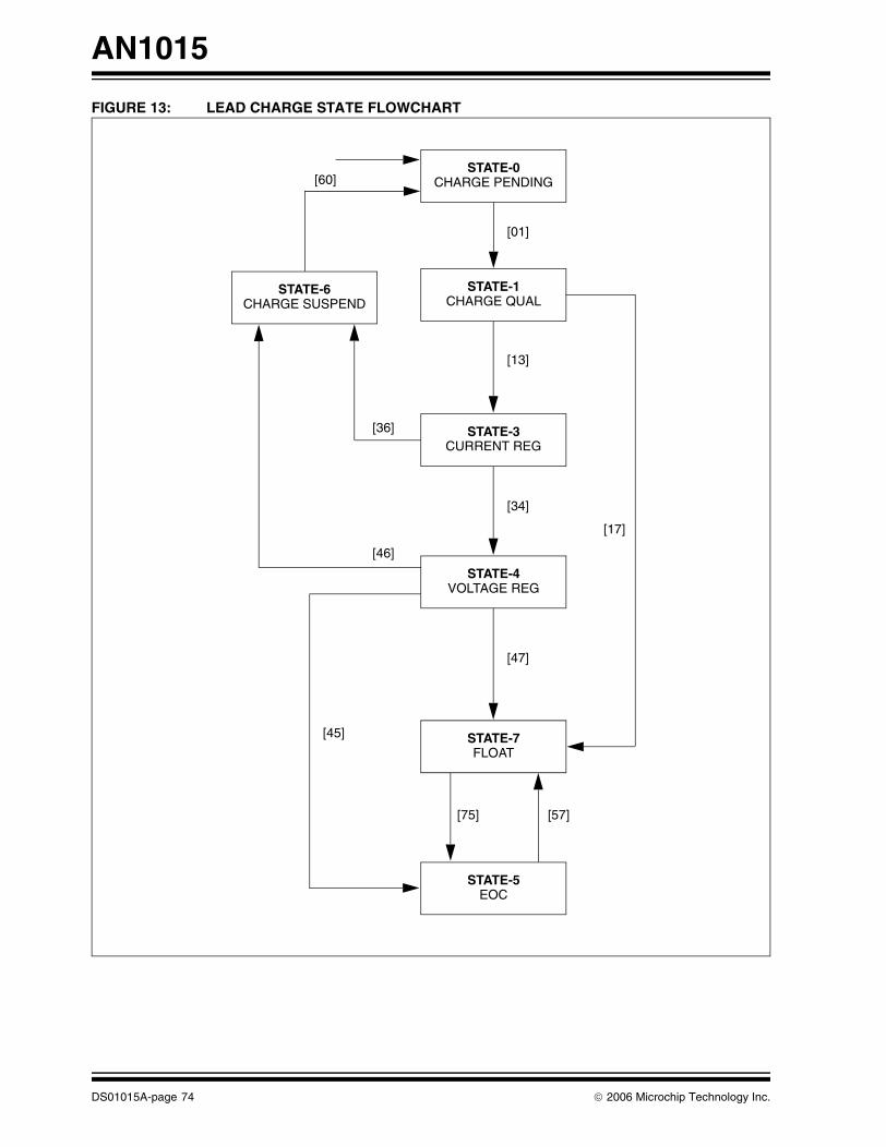
AN1015
FIGURE 13: LEAD CHARGE STATE FLOWCHART
STATE-0CHARGE PENDING
STATE-1CHARGE QUAL
STATE-3CURRENT REG
STATE-6CHARGE SUSPEND
STATE-4VOLTAGE REG
STATE-7FLOAT
STATE-5EOC
[60]
[01]
[36]
[13]
[34]
[46]
[17]
[47]
[75]
[45]
[57]
DS01015A-page 74 © 2006 Microchip Technology Inc.
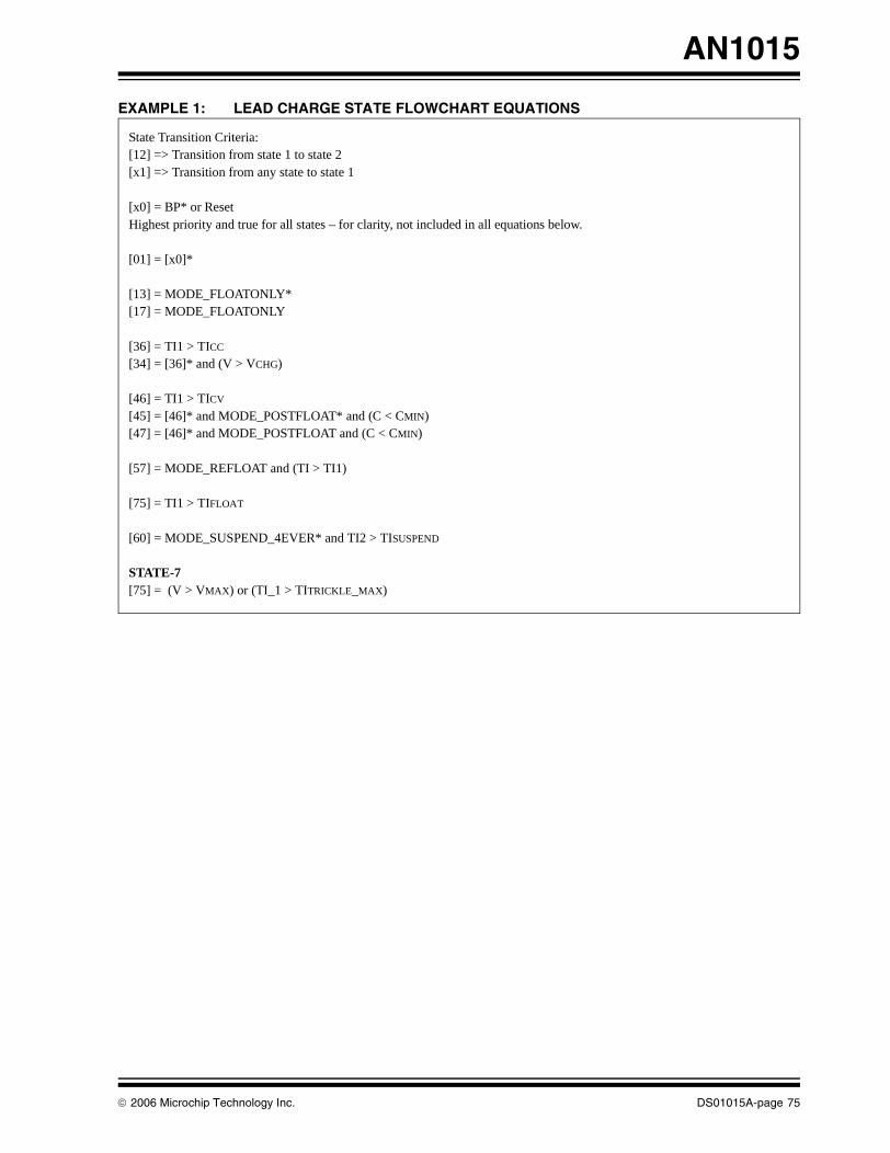
AN1015
EXAMPLE 1: LEAD CHARGE STATE FLOWCHART EQUATIONS
State Transition Criteria:[12] => Transition from state 1 to state 2[x1] => Transition from any state to state 1
[x0] = BP* or ResetHighest priority and true for all states – for clarity, not included in all equations below.
[01] = [x0]*
[13] = MODE_FLOATONLY*[17] = MODE_FLOATONLY
[36] = TI1 > TICC
[34] = [36]* and (V > VCHG)
[46] = TI1 > TICV
[45] = [46]* and MODE_POSTFLOAT* and (C < CMIN)[47] = [46]* and MODE_POSTFLOAT and (C < CMIN)
[57] = MODE_REFLOAT and (TI > TI1)
[75] = TI1 > TIFLOAT
[60] = MODE_SUSPEND_4EVER* and TI2 > TISUSPEND
STATE-7[75] = (V > VMAX) or (TI_1 > TITRICKLE_MAX)
© 2006 Microchip Technology Inc. DS01015A-page 75

AN1015
Charge State Initialization
This routine performs the initialization of variablesrequired by each individual charge state. Each chargestate will have a different set of triggers and variablesthat are required for exiting.
;-------------------------------------------------;--- charge state initialization;-------------------------------------------------chg_state_init: ; ;-----------------------------;--- chg_state_0_init();-----------------------------chg_state_0_init: ; call reg_off ; clrf r_adc_1_ofs ; movlw .0 ; goto chg_state_init_x_gpio_hi ;
;-----------------------------;--- chg_state_1_init();-----------------------------chg_state_1_init: ; movf r_adc_1_L, w ; movwf r_adc_1_ofs ; movlw .1 ; goto chg_state_init_x_gpio_hi ;
;-----------------------------;--- chg_state_2_init();-----------------------------chg_state_2_init: ; goto chg_state_0_init ;
;-----------------------------;--- chg_state_3_init();-----------------------------chg_state_3_init: ; call reg_load_chg ; movlw EE_CHG_TI_CC ; call load_timer_d1_ee ; movlw .3 ; goto chg_state_init_x_gpio_lo ;
;-----------------------------;--- chg_state_4_init();-----------------------------chg_state_4_init: ; call reg_load_chg ; movlw EE_CHG_TI_CV ; call load_timer_d1_ee ; movlw .4 ; goto chg_state_init_x_gpio_lo ;
;-----------------------------;--- chg_state_5_init();-----------------------------chg_state_5_init: ; call reg_off ; movlw EE_CHG_TI_REFLOAT ; call load_timer_d1_ee ; movlw .5 ; goto chg_state_init_x_gpio_hi ;
DS01015A-page 76 © 2006 Microchip Technology Inc.
AN1015
;-----------------------------;--- chg_state_6_init();-----------------------------chg_state_6_init: ; call reg_off ; movlw EE_CHG_TI_SUSPEND ; call load_timer_d2_ee ; movlw .6 ; goto chg_state_init_x_gpio_hi ;
;-----------------------------;--- chg_state_7_init();-----------------------------chg_state_7_init: ; call reg_load_flt ; movlw EE_CHG_TI_FLOAT ; call load_timer_d1_ee ; movlw .7 ; goto chg_state_init_x_gpio_lo ;
;---chg_state_init_x_gpio_hi: ; btfsc flag0_mode_gpio_cutoff ; bsf p_gpio ; goto chg_state_init_x_ ;chg_state_init_x_gpio_lo: ; btfsc flag0_mode_gpio_cutoff ; bcf p_gpio ;chg_state_init_x_: ;
movwf r_chg_state ; save state movf r_chg_state, w ; configure led1 addlw EE_LED1_CFG ; call ee_read_waddr ; call led_init_1 ; movf r_chg_state, w ; configure led2 addlw EE_LED2_CFG ; call ee_read_waddr ; call led_init_2 ;
movlw EE_CHG_TIME_0 ; call ee_read_waddr ; w = theshold from ee movwf r_chg_timer_a ;
return
© 2006 Microchip Technology Inc. DS01015A-page 77
AN1015
Check Triggers
This routine checks all the triggers that are required toexit the current charge state and enter into a differentone. The triggers, variables and equations for eachstate are described in the functional description.
;-----------------------------------------------------------;--- load_timer_d1() - load timer and reset pre-scaler;-----------------------------------------------------------load_timer_d1_ee: ; call ee_read_waddr ;load_timer_d1: ; movwf r_timer_d1 ; clrf r_timer_d ; bcf flag_chg_ti1_done ; return ; ;-----------------------------------------------------------;--- load_timer_d2() - load timer and reset pre-scaler; used as a "holdoff" or "minimum" timeout; therefore,; if setpoint==0, "done" flag set immediately; if setpoint<>0, "done" flag set when timer expires;-----------------------------------------------------------load_timer_d2_ee: ; call ee_read_waddr ;load_timer_d2: ; movwf r_timer_d2 ; clrf r_timer_d ; bcf flag_chg_ti2_done ; movf r_timer_d2, f ; btfsc r_status, Z ; bsf flag_chg_ti2_done ; set "done" if ==0 return ; ;---------------------------------------;--- check timer a;--- check timer b;--- check timer c;--- check timer d; status[Z]=1 if timer=0;---------------------------------------check_chg_timer_a: ; movlw r_chg_timer_a ; goto check_chg_timer_ ;check_chg_timer_b: ; movlw r_chg_timer_b ; goto check_chg_timer_ ;check_chg_timer_c: ; movlw r_chg_timer_c ; goto check_chg_timer_ ;check_chg_timer_d: ; movlw r_chg_timer_d ; goto check_chg_timer_ ;
check_chg_timer_: ; movwf r_fsr ; movf r_indf, f ; btfss r_status, Z ; decfsz r_indf, f ; nop ; return ;
DS01015A-page 78 © 2006 Microchip Technology Inc.
AN1015
;-----------------------------------------------------------;--- check_current() - compare current to threshold;; call:; w ee address of theshold; uses:; r_accB_L; r_accB_H; r_fsr; return:; r_status[C]=1 current <= threshold; r_status[C]=0 current > threshold;-----------------------------------------------------------check_current: ; call load_B_ee ;check_current_: movlw r_adc_1_H ; goto math_cmp_16 ;
;-----------------------------------------------------------;--- check_voltage() - compare voltage to threshold;; call:; w ee address of theshold; uses:; r_accB_L; r_accB_H; r_fsr; return:; r_status[C]=1 voltage <= threshold; r_status[C]=0 voltage > threshold;-----------------------------------------------------------check_voltage: ; call load_B_ee ; movlw r_adc_2_H ; goto math_cmp_16 ;
;-----------------------------------------------------------;--- check_temperature() - compare temperature to threshold;; call:; w ee address of theshold; uses:; r_accB_L; r_accB_H; r_fsr; return:; r_status[C]=1 temperature <= threshold; r_status[C]=0 temperature > threshold;-----------------------------------------------------------check_temperature: ; addlw -.1 ; accB_H = temp param call load_B_ee ; clrf r_accB_L ; movlw .6 ; call math_shift_BC ; accB = temp param * 4 movlw r_adc_3_H ; goto math_cmp_16 ;
;-------------------------------------------------;--- load_A_ee() - load accA from EE;-------------------------------------------------
© 2006 Microchip Technology Inc. DS01015A-page 79

AN1015
load_A_ee: ; call ee_read_waddr_ia ; movwf r_accA_L ; call ee_read_ia ; movwf r_accA_H ; return ; ;-------------------------------------------------;--- load_B_ee() - load accB from EE;-------------------------------------------------load_B_ee: ; call ee_read_waddr_ia ; movwf r_accB_L ; call ee_read_ia ; movwf r_accB_H ; return ; ;-----------------------------------------------------------;--- check_triggers() - compare a/d values to trigger levels;-----------------------------------------------------------check_triggers: ; clrf r_flags_2 ; pre-clear flags; movlw EE_CHG_T_PCHG ;; call check_temperature ;; rlf r_flags_2, f ; return ;
DS01015A-page 80 © 2006 Microchip Technology Inc.

AN1015
Regulate
The regulate routine controls the PWM so that therequired voltage and current are always delivered tothe battery. The charge state and feedback measure-
ments are used to determine if the PWM needs to beadjusted. If it does, then PWM_ADJUST is called tocalculate the correct new value, and PWM_SET iscalled to write that value to the PWM Control register.
;-----------------------------------------------------------;--- regulate();-----------------------------------------------------------#define REG_V_H2 .25 ; voltage - upper limit 2#define REG_V_H1 .6 ; voltage - upper limit 1#define REG_V_L1 .6 ; voltage - lower limit 1#define REG_V_L2 .50 ; voltage - upper limit 2
#define REG_C_NULL .5 ; current - null limit
#define REG_ADJ_P1 .12 ; pwm adjust#define REG_ADJ_P2 .10 ; pwm adjust#define REG_ADJ_P3 .5 ; pwm adjust#define REG_ADJ_P4 .1 ; pwm adjust regulate: ; btfss flag_reg_on ; regulation enabled ? goto regulate_x_ ; --- no, exit ...
btfss flag_reg_timer ; timer elapsed ? goto regulate_x_ ; --- no, exit ... bcf flag_reg_timer ;
btfss flag_adcset_1_rdy ; adc conversions done ? goto regulate_x ; --- no, chk adc & exit ...
;debug; call toggle
regulate_co: ; btfsc flag0_mode_vregco_dis ; goto regulate_co_x ; movlw EE_REG_VSAFETY ; call check_voltage ; btfss r_status, C ; goto reg_off ;regulate_co_x: ;
;---------------------------------------;--- voltage;---------------------------------------regulate_v: ; bcf flag_vreg_1 ; bcf flag_vreg_2 ; bcf flag_vreg ; bcf flag_neg ;
movlw r_adc_2_L ; call math_load_B ; accB = voltage call math_neg_B ; movlw r_reg_v ; call math_add_16_load_A ; accB = delta = reg_v - voltage btfss r_accB_H, 7 ; delta negative ? goto regulate_v_lo ; --- no, voltage <= vreg, skip ...
;--- V > VREGregulate_v_hi: ; bsf flag_vreg ; bsf flag_neg ;
© 2006 Microchip Technology Inc. DS01015A-page 81

AN1015
movlw EE_REG_VH ; call ee_read_waddr ; call math_add_8b ; btfss r_accB_H, 7 ; delta <= upper_limit ? goto regulate_v_x ; --- yes, go check current ... bsf flag_vreg_1 ;
movlw EE_REG_VHH_VH ; call ee_read_waddr ; call math_add_8b ; btfss r_accB_H, 7 ; delta <= upper_limit ? goto regulate_v_x ; --- yes, go check current ... bsf flag_vreg_2 ; V > LEVEL 2 !!
movlw EE_REG_P1 ; call ee_read_waddr ; goto regulate_adj ; --- no, make big adj (down) ;===(zones: A1,A2,A3,A4,A5);--- V <= VREGregulate_v_lo: ; call math_neg_B ;
movlw EE_REG_VL ; call ee_read_waddr ; call math_add_8b ; btfss r_accB_H, 7 ; delta <= upper_limit ? goto regulate_v_x ; --- yes, go check current ... bsf flag_vreg_1 ;
movlw EE_REG_VLL_VL ; call ee_read_waddr ; call math_add_8b ; btfss r_accB_H, 7 ; delta <= upper_limit ? goto regulate_v_x ; --- yes, go check current ... bsf flag_vreg_2 ; V > LEVEL 2 !!
regulate_v_x: ; btfsc flag_vreg_1 ; set flag_vreg if null zone goto regulate_v_x_ ; btfss flag_vreg_2 ; bsf flag_vreg ;regulate_v_x_: ;
;---------------------------------------;--- current;---------------------------------------regulate_c: ; movlw r_adc_1_L ; call math_load_B ; call math_neg_B ; movlw r_reg_c ; call math_add_16_load_A ; accB = delta = reg_c - current bcf flag_neg ; btfss r_accB_H, 7 ; goto $+3 ; bsf flag_neg ; current > reg_c level! (set flag) call math_neg_B ; delta = -delta (make it positive)
;--- delta_c >= 256 regulate_c_1: ; movf r_accB_H, f ; delta >= 256 mA btfsc r_status, Z ; goto regulate_c_1_x ; btfsc flag_neg ; goto regulate_adj_dn_1 ;===(zones: B5,C5,D5,E5
DS01015A-page 82 © 2006 Microchip Technology Inc.

AN1015
regulate_c_1_x: ;
;--- delta_c < 256 - voltage too high, non-nullregulate_c_2: ; btfss flag_vreg ; goto regulate_2_x ; btfsc flag_vreg_1 ; goto regulate_adj_dn_0 ;===(zones: B1,B2,B3,B4)regulate_2_x: ;
regulate_c_3: ; call math_neg_B ; delta_c = -delta_c (make it negative) movlw EE_REG_CNULL ; call ee_read_waddr ; call math_add_8b ; btfss r_accB_H, 7 ; goto regulate_x ;===(zones: C3,D3,E3) delta_c in null zone btfsc flag_neg ; goto regulate_adj_dn_0 ;===(zones: C4,D4,E4) current too high call math_neg_B ; delta = -delta (make it positive)regulate_c_3_x: ;
regulate_c_4: ; btfsc flag_vreg_2 ; goto regulate_c_4_x ; btfss flag_vreg_1 ; goto regulate_x ;===(zones: C1,C2) goto regulate_adj_up_0 ;===(zones: D1,D2)regulate_c_4_x: ;
regulate_c_5: ; movf r_accB_H, f ; delta <= -256 mA btfsc r_status, Z ; goto regulate_adj_up_0 ;===(zones: E2) movlw EE_REG_P3 ; call ee_read_waddr ; goto regulate_adj ;===(zones: E1)regulate_c_5_x: ;
regulate_adj_dn_1: ; movlw EE_REG_P2 ; call ee_read_waddr ; goto regulate_adj_dn ;regulate_adj_dn_0: ; movlw EE_REG_P4 ; call ee_read_waddr ;regulate_adj_dn: ; bsf flag_neg ; goto regulate_adj ;
regulate_adj_up_1: ; movlw EE_REG_P2 ; call ee_read_waddr ; goto regulate_adj_up ;regulate_adj_up_0: ; movlw EE_REG_P4 ; call ee_read_waddr ;regulate_adj_up: ; bcf flag_neg ;
regulate_adj: ; call pwm_adj ; call pwm_set ;
© 2006 Microchip Technology Inc. DS01015A-page 83
AN1015
regulate_x: ; bcf flag_adcset_1_rdy ; bsf flag_adcset_1_rq ;
regulate_x_: ; return ;
;---------------------------------------;--- reg_load();---------------------------------------
;--- reg_load_flt() - load float voltage (K or LUT)reg_load_flt: ; movlw EE_CHG_V_FLT_K ; btfsc flag0_mode_v_flt_k ; constant or lut ? goto reg_load_v ; --- constant ! call vlut_index_tcode ; --- lut ! call vlut_fetch_flt ; goto reg_load_c ;
;--- reg_load_flt() - load charge voltage (K or LUT)reg_load_chg: ; movlw EE_CHG_V_CHG_K ; btfsc flag0_mode_v_reg_k ; constant or lut ? goto reg_load_v ; --- constant ! call vlut_index_tcode ; --- lut ! call vlut_fetch_chg ; goto reg_load_c ;
reg_load_v: ; call load_B_ee ; movlw r_reg_v ; call math_move_B ;
reg_load_c: ; movlw EE_CHG_C ; call load_B_ee ; movlw r_reg_c ; call math_move_B ;; goto reg_on ;
;---------------------------------------;--- reg_on() - regulation on;---------------------------------------reg_on: ; bsf flag_reg_on ; bsf r_status, RP1 ; bcf r_pwmclk, PWMASE ; bcf r_status, RP1 ; return ;
;---------------------------------------;--- reg_off() - regulation off;---------------------------------------reg_off: ; bcf flag_reg_on ; clrf r_reg_c ; clrf r_reg_c+1 ; clrf r_reg_v ; clrf r_reg_v+1 ; clrf r_pwm_L ; clrf r_pwm_H ; call pwm_set ; return ;
DS01015A-page 84 © 2006 Microchip Technology Inc.

AN1015
Math Functions
These are random math routines used by the firmware.
;-----------------------------------------------------;--- math_add_8b() - add 8-bit positive value to accB;-----------------------------------------------------math_add_8b: ; movwf r_accA_L ; clrf r_accA_H ; goto math_add_16 ;
;-----------------------------------------------------------;--- math_mul_16_prep();; function:; *WREG - 16-bit operand;-----------------------------------------------------------math_mul_16_prep: ; call math_load_A ;math_mul_16_prep_: ; movlw .16 ;
;-----------------------------------------------------------;--- math_mul_16;; function:; 16x16 multiplication;; call:; WREG - count/shift ops; op1: accA; op2: accD;; result:; accB,accC = accA * accD;----------------------------------------------------------- math_mul_16: ; movwf r_count_1 ; clrf r_accB_H ; clear result accumulator clrf r_accB_L ; clrf r_accC_H ; clrf r_accC_L ;
math_mul_16_loop: ; rrf r_accD_H, F ; shift operand2 lsb into C rrf r_accD_L, F ; btfss r_status, C ; C = 1? goto math_mul_16_shift ; --- no, go shift ...
math_mul_16_add: ; call math_add_16 ;
math_mul_16_shift: ; rrf r_accB_H, F ; SHIFT result accumulator rrf r_accB_L, F ; rrf r_accC_H, F ; rrf r_accC_L, F ; decfsz r_count_1, F ; goto math_mul_16_loop ; loop
retlw 0 ;
© 2006 Microchip Technology Inc. DS01015A-page 85
AN1015
;-----------------------------------------------------------;--- div32; operands:; dividend - accA,accB; divisor - accC;; result:; quotient - accB; remainder - accA; overflow - WREG=0 else WREG=1 ?;-----------------------------------------------------------math_div_32: ; movf r_accC_L, W ; subwf r_accA_L, W ; movf r_accC_H, W ; btfss r_status, C ; incf r_accC_H, W ; subwf r_accA_H, W ; btfsc r_status, C ; retlw 0 ; overflow or division by zero
movlw .16 ; movwf r_count_1 ;math_div_32_loop: ; bcf r_status, C ; rlf r_accB_L, F ; shift dividend (accA,accB << 1) rlf r_accB_H, F ; rlf r_accA_L, F ; rlf r_accA_H, F ;
btfsc r_status, C ; if carry, go subtract goto math_div_32_sub ;
movf r_accC_L, W ; subwf r_accA_L, W ; movf r_accC_H, W ; btfss r_status, C ; incf r_accC_H, W ; subwf r_accA_H, W ; btfss r_status, C ; if smaller than divisor, skip to next goto math_div_32_next ;
math_div_32_sub: ; movf r_accC_L, W ; subtract divisor from high subwf r_accA_L, F ; movf r_accC_H, W ; btfss r_status, C ; incf r_accC_H, W ; subwf r_accA_H, F ; bsf r_accB_L, 0 ;
math_div_32_next: ; decfsz r_count_1, F ; goto math_div_32_loop ; retlw 1 ; no more overflow possible
;-----------------------------------------------------------;--- math_add_16();; function:; add 16-bit operands;; call:; op1: accA; op2: accB
DS01015A-page 86 © 2006 Microchip Technology Inc.

AN1015
;; result:
; accB = accA + accB;-----------------------------------------------------------math_add_16_load_A: ; call math_load_A ;math_add_16: ; movf r_accA_L, w ; addwf r_accB_L, f ; btfsc r_status, C ; incf r_accB_H, f ; movf r_accA_H, w ; addwf r_accB_H, f ; retlw 0 ;
;-----------------------------------------------------------;--- math_neg_B();; function:
; accB = -accB;-----------------------------------------------------------math_neg_B: ; comf r_accB_L, f ; incf r_accB_L, f ; btfsc r_status, Z ; decf r_accB_H, f ; comf r_accB_H, f ; retlw 0 ;
;-----------------------------------------------------------;--- math_cmp_16();; function:; compare 2 16-bit values ; 1: accB 2: *WREG;; call:; *WREG: operand A (msb); accB: operand B;; result:; status[C]=1: accB >= *WREG; status[C]=0: accB < *WREG;-----------------------------------------------------------math_cmp_16: ; movwf r_fsr ; movf r_indf, w ; subwf r_accB_H, w ; btfss r_status, Z ; return ; decf r_fsr, f ; movf r_indf, w ; subwf r_accB_L, w ; return ;
;-----------------------------------------------------------;--- math_load_ utilities; *WREG = lsb of source data;-----------------------------------------------------------
;--- math_load_D()math_load_D: ; movwf r_fsr ;
© 2006 Microchip Technology Inc. DS01015A-page 87
AN1015
math_load_D_: ; movf r_indf, w ; movwf r_accD_L ; incf r_fsr, f ; movf r_indf, w ; movwf r_accD_H ; goto math_load_x ;
;--- math_load_C()math_load_C: ; movwf r_fsr ;math_load_C_: ; movf r_indf, w ; movwf r_accC_L ; incf r_fsr, f ; movf r_indf, w ; movwf r_accC_H ; goto math_load_x ;
;--- math_load_B()math_load_B: ; movwf r_fsr ;math_load_B_: ; movf r_indf, w ; movwf r_accB_L ; incf r_fsr, f ; movf r_indf, w ; movwf r_accB_H ; goto math_load_x ;
;--- math_load_A()math_load_A: ; movwf r_fsr ;math_load_A_: ; movf r_indf, w ; movwf r_accA_L ; incf r_fsr, f ; movf r_indf, w ; movwf r_accA_H ;math_load_x: ; incf r_fsr, f ; return ;
;--- math_move_B: ; movwf r_fsr ;math_move_B_: ; movf r_accB_L, w ; movwf r_indf ; incf r_fsr, f ; movf r_accB_H, w ; goto math_move_x ;
;--- math_move_D: ; movwf r_fsr ;math_move_D_: ; movf r_accD_L, w ; movwf r_indf ; incf r_fsr, f ; movf r_accD_H, w ; goto math_move_x ;
DS01015A-page 88 © 2006 Microchip Technology Inc.
AN1015
math_move_x: ; movwf r_indf ; incf r_fsr, f ; return ;
;--- math_shift_BC: ; movwf r_count_1 ;math_shift_BC_loop: ; bcf r_status, C ; rrf r_accB_H, f ; rrf r_accB_L, f ; rrf r_accC_H, f ; rrf r_accC_L, f ; decfsz r_count_1, f ; goto math_shift_BC_loop ; return ;
org 0x7d0chg_state_svc_jumptable: ; movlw high $ ; movwf r_pclath ; movf r_chg_state, w ; andlw 0x0f ; addwf r_pcl, f ; goto chg_state_0 ; goto chg_state_1 ; goto chg_state_2 ; goto chg_state_3 ; goto chg_state_4 ; goto chg_state_5 ; goto chg_state_6 ; goto chg_state_7 ; goto chg_state_0_init ; goto chg_state_1_init ; goto chg_state_2_init ; goto chg_state_3_init ; goto chg_state_4_init ; goto chg_state_5_init ; goto chg_state_6_init ; goto chg_state_7_init ;#if chg_state_svc_jumptable >> 8 != $>>8 error "jump table page violation: chg_state_svc_jumptable"#endif
© 2006 Microchip Technology Inc. DS01015A-page 89

AN1015
Default EEPROM Values
This sets the default values for the EEPROMparameters. Note that the internal names of EEPROMparameters may vary from the data sheet andPowerTool 200 software names. The PowerTool 200software names are used in the functional descriptionsection.
;---------------------------------------;--- EEPROM DEFAULT;---------------------------------------
org 0x2100 DE 0x02, 0x00 ; pattern DE .1 ; ncells DE "microchp" ; manuf name DE "16HV785 " ; device name DE low .2000, high .2000 ; capacity DE .19 ; pwm DE 0x01 ; mode DE 0x21 ; mode2 DE .00 ; oscillator trim
org 0x2120 DE 0x08, 0x18, 0x28, 0x38 ; LED1 CONFIG DE 0x48, 0x58, 0x68, 0x78 ; LED1 CONFIG (cont) DE 0x08, 0x18, 0x28, 0x38 ; LED2 CONFIG DE 0x48, 0x58, 0x68, 0x78 ; LED2 CONFIG (cont)
org 0x2134 DE .12, .10, .05, .01 ; regulation: pwm adj values DE .19, .06, .06, .44 ; regulation: voltage zone thresholds DE .6 ; regulation: current zone thresholds DE low .2900, high .2900 ; regulation: v_safety (lion)
org 0x2143 DE low .1500, high .1500 ; chg_c DE low .1000, high .1000 ; chg_c_float DE low .150, high .150 ; chg_c_min DE .90 ; chg_ti_cc (90=6hr) DE .90 ; chg_ti_cv DE .15 ; chg_ti_float DE .15 ; chg_ti_refloat DE .0 ; chg_ti_suspend DE low .2450, high .2450 ; chg_v_chg DE low .2275, high .2275 ; chg_v_flt DE low .0500, high .0500 ; chg_v_min_bp
org 0x215c DE .20, .20, .00, .00, .00, .00 ; chg_time DE .000, .128 ; battid_min, _max
org 0x216c DE low .0248, high .0248 ; adc_cal_0 (reference) DE low .2553, high .2553 ; adc_cal_1 (current) DE low .3412, high .3412 ; adc_cal_2 (voltage) DE low .8192, high .8192 ; adc_cal_3 (temperature) DE low .6407, high .6407 ; adc_cal_4 (battid) DE .100 ; shunt DE .112 ; temperature default
DS01015A-page 90 © 2006 Microchip Technology Inc.

AN1015
org 0x217C DE .8 ; TLUT - length DE .38, .48, .61, .79 ; TLUT - temp axis DE .105, .183, .207 ; TLUT - temp axis (cont) DE low -.23362, high -.23362 ; TLUT - slope - 0 DE low .1418, high .1418 ; TLUT - yint - 0 DE low -.19864, high -.19864 ; TLUT - slope - 1 DE low .1352, high .1352 ; TLUT - yint - 1 DE low -.15709, high -.15709 ; TLUT - slope - 2 DE low .1255, high .1255 ; TLUT - yint - 2 DE low -.12572, high -.12572 ; TLUT - slope - 3 DE low .1162, high .1162 ; TLUT - yint - 3 DE low -.10206, high -.10206 ; TLUT - slope - 4 DE low .1071, high .1071 ; TLUT - yint - 4 DE low -.8631, high -.8631 ; TLUT - slope - 5 DE low .990, high .990 ; TLUT - yint - 5 DE low -.10154, high -.10154 ; TLUT - slope - 6 DE low .1127, high .1127 ; TLUT - yint - 6 DE low -.12875, high -.12875 ; TLUT - slope - 7 DE low .1402, high .1402 ; TLUT - yint - 7
org 0x21AA DE 0x1E ; mode_3 DE .10 ; vlut_n - vlut length;--- vlut_t DE .025, .050, .075, .100 ; -10, 0, 10, 20 DE .113, .125, .137, .150 ; 25, 30, 35, 40 DE .175 ; 50
;--- vlut chg DE low .2760, high .2760 ; DE low .2770, high .2770 ; DE low .2650, high .2650 ; DE low .2590, high .2590 ; DE low .2530, high .2530 ; DE low .2500, high .2500 ; DE low .2470, high .2470 ; DE low .2410, high .2410 ; DE low .2350, high .2350 ; DE low .2250, high .2250 ;
;--- vlut flt DE low .2380, high .2380 ; DE low .2370, high .2370 ; DE low .2350, high .2350 ; DE low .2330, high .2330 ; DE low .2310, high .2310 ; DE low .2300, high .2300 ; DE low .2290, high .2290 ; DE low .2270, high .2270 ; DE low .2250, high .2250 ; DE low .2200, high .2200 ;
end
© 2006 Microchip Technology Inc. DS01015A-page 91

AN1015
MEMORY MAP
TABLE 11: EEPROM MEMORY MAP
NameLocation
LenDefault
Units DescriptionDec Hex Dec Hex
PATTERN 1 0001 2 1 1 coded Pattern ID (arbitrary)
NCELLS 1 01 1 1 1 cells Number of cells
MANUF_NAME 3 03 8 — — ASCII Manufacturer’s name “Microchip”
DEV_NAME 11 0B 8 — — ASCII Device name “16HV785”
CAPACITY 19 13 2 800 320 mAh Capacity
PWM_FREQ 21 15 1 19 13 coded PWM frequency (e.g. 19 = 400 kHz)
MODE 22 16 1 1 01 coded Mode – control flags
MODE2 23 17 1 32 20 coded Mode – control flags
OSC_TRIM 24 18 1 0 0 coded Oscillator trim – signed value +/-10%
Reserved 25 19 7 x x x
SUB-CONFIG 32 20 32
LED1_CFG_0 32 20 1 8 08 coded LED1 configuration – state 0
LED1_CFG_1 33 21 1 24 18 coded LED1 configuration – state 1
LED1_CFG_2 34 22 1 40 28 coded LED1 configuration – state 2
LED1_CFG_3 35 23 1 56 38 coded LED1 configuration – state 3
LED1_CFG_4 36 24 1 72 48 coded LED1 configuration – state 4
LED1_CFG_5 37 25 1 88 58 coded LED1 configuration – state 5
LED1_CFG_6 38 26 1 104 68 coded LED1 configuration – state 6
LED1_CFG_7 39 27 1 120 78 coded LED1 configuration – state 7
LED2_CFG_0 40 28 1 8 08 coded LED2 configuration – state 0
LED2_CFG_1 41 29 1 24 18 coded LED2 configuration – state 1
LED2_CFG_2 42 2A 1 40 28 coded LED2 configuration – state 2
LED2_CFG_3 43 2B 1 56 38 coded LED2 configuration – state 3
LED2_CFG_4 44 2C 1 72 48 coded LED2 configuration – state 4
LED2_CFG_5 45 2D 1 88 58 coded LED2 configuration – state 5
LED2_CFG_6 46 2E 1 104 68 coded LED2 configuration – state 6
LED2_CFG_7 47 2F 1 120 78 coded LED2 configuration – state 7
Reserved 48 30 4 x x x
SUB-LED 52 34 20
REG_P1 52 34 1 12 0C count Regulation – control PWM adj
REG_P2 53 35 1 10 0A count Regulation – control PWM adj
REG_P3 54 36 1 5 05 count Regulation – control PWM adj
REG_P4 55 37 1 1 01 count Regulation – control PWM adj
REG_VHH_VH 56 38 1 19 13 mV Regulation – voltage zone limit
REG_VH 57 39 1 6 06 mV Regulation – voltage zone limit
REG_VL 58 3A 1 6 06 mV Regulation – voltage zone limit
REG_VLL_VL 59 3B 1 44 2C mV Regulation – voltage zone limit
REG_CNULL 60 3C 1 5 05 mA Regulation – current null limit
REG_VSAFETY 61 3D 2 4350 10FE mV Regulation – voltage limit – shutdown
Reserved 63 3F 4 x x x
DS01015A-page 92 © 2006 Microchip Technology Inc.
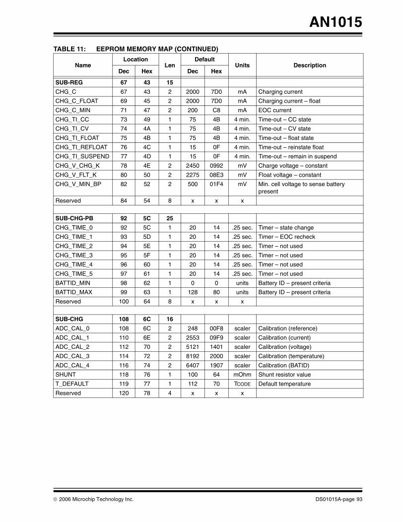
AN1015
SUB-REG 67 43 15
CHG_C 67 43 2 2000 7D0 mA Charging current
CHG_C_FLOAT 69 45 2 2000 7D0 mA Charging current – float
CHG_C_MIN 71 47 2 200 C8 mA EOC current
CHG_TI_CC 73 49 1 75 4B 4 min. Time-out – CC state
CHG_TI_CV 74 4A 1 75 4B 4 min. Time-out – CV state
CHG_TI_FLOAT 75 4B 1 75 4B 4 min. Time-out – float state
CHG_TI_REFLOAT 76 4C 1 15 0F 4 min. Time-out – reinstate float
CHG_TI_SUSPEND 77 4D 1 15 0F 4 min. Time-out – remain in suspend
CHG_V_CHG_K 78 4E 2 2450 0992 mV Charge voltage – constant
CHG_V_FLT_K 80 50 2 2275 08E3 mV Float voltage – constant
CHG_V_MIN_BP 82 52 2 500 01F4 mV Min. cell voltage to sense battery present
Reserved 84 54 8 x x x
SUB-CHG-PB 92 5C 25
CHG_TIME_0 92 5C 1 20 14 .25 sec. Timer – state change
CHG_TIME_1 93 5D 1 20 14 .25 sec. Timer – EOC recheck
CHG_TIME_2 94 5E 1 20 14 .25 sec. Timer – not used
CHG_TIME_3 95 5F 1 20 14 .25 sec. Timer – not used
CHG_TIME_4 96 60 1 20 14 .25 sec. Timer – not used
CHG_TIME_5 97 61 1 20 14 .25 sec. Timer – not used
BATTID_MIN 98 62 1 0 0 units Battery ID – present criteria
BATTID_MAX 99 63 1 128 80 units Battery ID – present criteria
Reserved 100 64 8 x x x
SUB-CHG 108 6C 16
ADC_CAL_0 108 6C 2 248 00F8 scaler Calibration (reference)
ADC_CAL_1 110 6E 2 2553 09F9 scaler Calibration (current)
ADC_CAL_2 112 70 2 5121 1401 scaler Calibration (voltage)
ADC_CAL_3 114 72 2 8192 2000 scaler Calibration (temperature)
ADC_CAL_4 116 74 2 6407 1907 scaler Calibration (BATID)
SHUNT 118 76 1 100 64 mOhm Shunt resistor value
T_DEFAULT 119 77 1 112 70 TCODE Default temperature
Reserved 120 78 4 x x x
TABLE 11: EEPROM MEMORY MAP (CONTINUED)
NameLocation
LenDefault
Units DescriptionDec Hex Dec Hex
© 2006 Microchip Technology Inc. DS01015A-page 93

AN1015
SUB-ADC 124 7C 16
T_LUT_N 124 7C 1 8 08 entries Temperature LUT – length (max. = 8)
T_LUT_T_0 125 7D 1 38 26 TCODE Temperature LUT – T0 (T_LUT_N – 1 entry)
T_LUT_T_1 126 7E 1 48 30 TCODE Temperature LUT – T1
T_LUT_T_2 127 7F 1 61 3D TCODE Temperature LUT – T2
T_LUT_T_3 128 80 1 79 4F TCODE Temperature LUT – T3
T_LUT_T_4 129 81 1 105 69 TCODE Temperature LUT – T4
T_LUT_T_5 130 82 1 183 B7 TCODE Temperature LUT – T5
T_LUT_T_6 131 83 1 207 CF TCODE Temperature LUT – T6
T_LUT_M_0 132 84 2 -23362 A4BE scaler Temperature LUT – T0 slope (T_LUT_N entries)
T_LUT_B_0 134 86 2 1418 058A scaler Temperature LUT – T0 Y-intercept
T_LUT_M_1 136 88 2 -19864 B268 scaler Temperature LUT – T1 slope
T_LUT_B_1 138 8A 2 1352 0548 scaler Temperature LUT – T1 Y-intercept
T_LUT_M_2 140 8C 2 -15709 C2A3 scaler Temperature LUT – T2 slope
T_LUT_B_2 142 8E 2 1255 04E7 scaler Temperature LUT – T2 Y-intercept
T_LUT_M_3 144 90 2 -12572 CEE4 scaler Temperature LUT – T3 slope
T_LUT_B_3 146 92 2 1162 048A scaler Temperature LUT – T3 Y-intercept
T_LUT_M_4 148 94 2 -10206 D822 scaler Temperature LUT – T4 slope
T_LUT_B_4 150 96 2 1071 042F scaler Temperature LUT – T4 Y-intercept
T_LUT_M_5 152 98 2 -8631 DE49 scaler Temperature LUT – T5 slope
T_LUT_B_5 154 9A 2 990 03DE scaler Temperature LUT – T5 Y-intercept
T_LUT_M_6 156 9C 2 -10154 D856 scaler Temperature LUT – T6 slope
T_LUT_B_6 158 9E 2 1127 0467 scaler Temperature LUT – T6 Y-intercept
T_LUT_M_7 160 A0 2 -12875 CDB5 scaler Temperature LUT – T7 slope
T_LUT_B_7 162 A2 2 1402 057A scaler Temperature LUT – T7 Y-intercept
TABLE 11: EEPROM MEMORY MAP (CONTINUED)
NameLocation
LenDefault
Units DescriptionDec Hex Dec Hex
DS01015A-page 94 © 2006 Microchip Technology Inc.

AN1015
SUB-T LUT 164 A4 40
MODE_3 170 AA 1 0 0 bits Mode bits
VLUT_N 171 AB 1 10 A
T_VLUT_0 172 AC 1 0 0 TCODE VLUT – temperature vector
T_VLUT_1 173 AD 1 25 19 TCODE
T_VLUT_2 174 AE 1 50 32 TCODE
T_VLUT_3 175 AF 1 75 4B TCODE
T_VLUT_4 176 B0 1 100 64 TCODE
T_VLUT_5 177 B1 1 113 70 TCODE
T_VLUT_6 178 B2 1 125 7D TCODE
T_VLUT_7 179 B3 1 150 96 TCODE
T_VLUT_8 180 B4 1 175 AF TCODE
V_VLUT_CHG_0 181 B5 2 2760 AC8 mV VLUT – charging
V_VLUT_CHG_1 183 B7 2 2700 A8C mV
V_VLUT_CHG_2 185 B9 2 2650 A5A mV
V_VLUT_CHG_3 187 BB 2 2590 A1E mV
V_VLUT_CHG_4 189 BD 2 2530 9E2 mV
V_VLUT_CHG_5 191 BF 2 2500 9C4 mV
V_VLUT_CHG_6 193 C1 2 2470 9A6 mV
V_VLUT_CHG_7 195 C3 2 2410 96A mV
V_VLUT_CHG_8 197 C5 2 2350 92E mV
V_VLUT_CHG_9 199 C7 2 2250 8CA mV
V_VLUT_FLT_0 201 C9 2 2380 94C mV VLUT – float
V_VLUT_FLT_1 203 CB 2 2370 942 mV
V_VLUT_FLT_2 205 CD 2 2350 92E mV
V_VLUT_FLT_3 207 CF 2 2330 91A mV
V_VLUT_FLT_4 209 D1 2 2310 906 mV
V_VLUT_FLT_5 211 D3 2 2300 8FC mV
V_VLUT_FLT_6 213 D5 2 2290 8F2 mV
V_VLUT_FLT_7 215 D7 2 2270 8DE mV
V_VLUT_FLT_8 217 D9 2 2250 8CA mV
V_VLUT_FLT_9 219 DB 2 2200 898 mV
SUB-T LUT 221 DD 51
TOTAL 188
TABLE 11: EEPROM MEMORY MAP (CONTINUED)
NameLocation
LenDefault
Units DescriptionDec Hex Dec Hex
© 2006 Microchip Technology Inc. DS01015A-page 95

AN1015
MODE Registers
TABLE 12: MODE
TABLE 13: MODE2
TABLE 14: MODE3
Bit Name Description
7
6 gpio_cutoff 1 = Enable GPIO cutoff logic
5
4
3
2 bpres_battid 1 = Battery present on BATID
1 bpres_v 1 = Battery present on voltage sense
0 bpres_always 1 = Battery present always
Bit Name Description
7 cofs_dis 1 = Disable auto-offset current cancellation
6 osc_out 1 = Enable clock output (256) on BATID after Reset
5 temp_k 1 = Use constant temperature from EEPROM
4
3
2
1 vregco_dis 1 = Disable voltage cutoff in regulator
0 pwmas_dis 1 = Disable PWM auto-shutdown
Bit Name Description
7
6
5 suspend_4ever Suspend indefinitely – until Reset or battery removed, etc.
4 refloat Enable “refloat” – entered from EOC state
3 postfloat Enable float after CC, CV states
2 v_flt_k Use fixed float voltage (otherwise use VLUT)
1 v_chg_k Use fixed charging voltage (otherwise use VLUT)
0 float Skip to float state immediately
DS01015A-page 96 © 2006 Microchip Technology Inc.

AN1015
RAM
TABLE 15: RAM
Name Dec Hex Len Units Description
r_mode 32 20 1 bits Operational mode register
r_chg_state 33 21 1 int Charge Controller “state”
r_adc_0_L 34 22 1 units ADC result – channel 0 (VREF)
r_adc_0_H 35 23 1
r_adc_1_L 36 24 1 mA ADC result – channel 1 (CURRENT)
r_adc_1_H 37 25 1
r_adc_2_L 38 26 1 mV ADC result – channel 2 (VOLTAGE)
r_adc_2_H 39 27 1
r_adc_3_L 40 28 1 TCODE ADC result – channel 3 (TEMP)
r_adc_3_H 41 29 1
r_adc_4_L 42 2A 1 units ADC result – channel 4 (BATID)
r_adc_4_H 43 2B 1
r_pwm_L 44 2C 1 int PWM setting
r_pwm_H 45 2D 1 PWM setting
r_reg_c 46 2E 2 mA Regulation target: current (mA)
r_reg_v 48 30 2 mV Regulation target: voltage (mV)
r_comm_reg_0 50 32 1 N/A Indirect Address register
r_comm_reg_1 51 33 1 N/A Status
r_comm_reg_2 52 34 1 N/A Configuration flags
r_comm_reg_3 53 35 1 N/A Command flags
r_comm_reg_4 54 36 1 N/A Data lo
r_comm_reg_5 55 37 1 N/A Data hi
r_comm_reg_6 56 38 1 N/A
r_comm_reg_7 57 39 1 N/A
r_sim 58 3A 1 N/A
r_chg_timer_a 59 3B 1 .25 sec. Hysteresis timer
r_chg_timer_b 60 3C 1 .25 sec. Hysteresis timer
r_chg_timer_c 61 3D 1 .25 sec. Hysteresis timer
r_chg_timer_d 62 3E 1 .25 sec. Hysteresis timer
r_temp_1 63 3F 1 N/A Location sensitive (init ram clear)
r_temp_2 64 40 1 N/A
r_temp_3 65 41 1 N/A
r_temp_4 66 42 1 N/A
r_tempi_1 67 43 1 N/A Temporary register for ISR
r_timer_a1 68 44 1 N/A
r_timer_b 69 45 1 N/A
r_timer_b1 70 46 1 N/A
r_timer_c 71 47 1 N/A
r_timer_d 72 48 1 sec.
r_timer_d1 73 49 1 4 min.
r_led_config_1 74 4A 1 N/A
r_led_contrl_1 75 4B 1 N/A
r_led_config_2 76 4C 1 N/A
© 2006 Microchip Technology Inc. DS01015A-page 97

AN1015
r_led_contrl_2 77 4D 1 N/A
r_adc_control 78 4E 1 N/A ADC control
r_adc_raw_L 79 4F 1 N/A
r_adc_raw_H 80 50 1 N/A
r_count_1 81 51 1 N/A
r_accD_L 82 52 1 N/A Math – accumulator – D
r_accD_H 83 53 1 N/A
r_accC_L 84 54 1 N/A Math – accumulator – C
r_accC_H 85 55 1 N/A
r_accB_L 86 56 1 N/A Math – accumulator – B
r_accB_H 87 57 1 N/A
r_accA_L 88 58 1 N/A Math – accumulator – A
r_accA_H 89 59 1 N/A
r_comm_count 90 5A 1 N/A
r_comm_data 91 5B 1 N/A
r_comm_flags 92 5C 1 N/A
r_comm_data_cmnd 93 5D 1 N/A
r_mode2 94 5E 1 bits Operational mode flags
unused 95 5F 1 N/A
r_adc_accum 96 60 2 N/A
r_adc_accum_count 98 62 1 N/A
r_adc_avg 99 63 2 N/A
r_adc_shadow 101 65 2 units
r_adc_1_ofs 103 67 1 mA
r_tcode 104 68 1 mV NiMh -dv reference
unused 106 6A 5 TCODE NiMh dtdt reference
r_mode3 110 6E 1 bits Operational mode bits
r_timer_d2 111 6F 1 4 min. Timer – min. timer – NiMh algorithm
r_shadow_1 112 70 1 N/A Debug
r_shadow_2 113 71 1 N/A Debug
r_shadow_3 114 72 1 N/A Debug
r_flags_1 115 73 1 bits Assorted bit flags
r_flags_2 116 74 1 bits Assorted bit flags
r_flags_3 117 75 1 bits Assorted bit flags
r_flags_4 118 76 1 bits Assorted bit flags
r_flags_5 119 77 1 bits Assorted bit flags
r_flags_6 120 78 1 bits Assorted bit flags
r_isr_w 121 79 1 N/A Interrupt context
r_isr_status 122 7A 1 N/A Interrupt context
r_isr_pclath 123 7B 1 N/A Interrupt context
r_isr_fsr 124 7C 1 N/A Interrupt context
r_ee_data 125 7D 1 N/A EEPROM data
r_ee_addr 126 7E 1 N/A EEPROM address
r_tempc_1 127 7F 1 N/A Temporary register
TABLE 15: RAM (CONTINUED)
Name Dec Hex Len Units Description
DS01015A-page 98 © 2006 Microchip Technology Inc.
Note the following details of the code protection feature on Microchip devices:
• Microchip products meet the specification contained in their particular Microchip Data Sheet.
• Microchip believes that its family of products is one of the most secure families of its kind on the market today, when used in the intended manner and under normal conditions.
• There are dishonest and possibly illegal methods used to breach the code protection feature. All of these methods, to our knowledge, require using the Microchip products in a manner outside the operating specifications contained in Microchip’s Data Sheets. Most likely, the person doing so is engaged in theft of intellectual property.
• Microchip is willing to work with the customer who is concerned about the integrity of their code.
• Neither Microchip nor any other semiconductor manufacturer can guarantee the security of their code. Code protection does not mean that we are guaranteeing the product as “unbreakable.”
Code protection is constantly evolving. We at Microchip are committed to continuously improving the code protection features of ourproducts. Attempts to break Microchip’s code protection feature may be a violation of the Digital Millennium Copyright Act. If such actsallow unauthorized access to your software or other copyrighted work, you may have a right to sue for relief under that Act.
Information contained in this publication regarding deviceapplications and the like is provided only for your convenienceand may be superseded by updates. It is your responsibility toensure that your application meets with your specifications.MICROCHIP MAKES NO REPRESENTATIONS OR WAR-RANTIES OF ANY KIND WHETHER EXPRESS OR IMPLIED,WRITTEN OR ORAL, STATUTORY OR OTHERWISE,RELATED TO THE INFORMATION, INCLUDING BUT NOTLIMITED TO ITS CONDITION, QUALITY, PERFORMANCE,MERCHANTABILITY OR FITNESS FOR PURPOSE.Microchip disclaims all liability arising from this information andits use. Use of Microchip devices in life support and/or safetyapplications is entirely at the buyer’s risk, and the buyer agreesto defend, indemnify and hold harmless Microchip from any andall damages, claims, suits, or expenses resulting from suchuse. No licenses are conveyed, implicitly or otherwise, underany Microchip intellectual property rights.
© 2006 Microchip Technology Inc.
Trademarks
The Microchip name and logo, the Microchip logo, Accuron, dsPIC, KEELOQ, microID, MPLAB, PIC, PICmicro, PICSTART, PRO MATE, PowerSmart, rfPIC, and SmartShunt are registered trademarks of Microchip Technology Incorporated in the U.S.A. and other countries.
AmpLab, FilterLab, Migratable Memory, MXDEV, MXLAB, PICMASTER, SEEVAL, SmartSensor and The Embedded Control Solutions Company are registered trademarks of Microchip Technology Incorporated in the U.S.A.
Analog-for-the-Digital Age, Application Maestro, dsPICDEM, dsPICDEM.net, dsPICworks, ECAN, ECONOMONITOR, FanSense, FlexROM, fuzzyLAB, In-Circuit Serial Programming, ICSP, ICEPIC, Linear Active Thermistor, MPASM, MPLIB, MPLINK, MPSIM, PICkit, PICDEM, PICDEM.net, PICLAB, PICtail, PowerCal, PowerInfo, PowerMate, PowerTool, Real ICE, rfLAB, rfPICDEM, Select Mode, Smart Serial, SmartTel, Total Endurance, UNI/O, WiperLock and Zena are trademarks of Microchip Technology Incorporated in the U.S.A. and other countries.
SQTP is a service mark of Microchip Technology Incorporated in the U.S.A.
All other trademarks mentioned herein are property of their respective companies.
© 2006, Microchip Technology Incorporated, Printed in the U.S.A., All Rights Reserved.
Printed on recycled paper.
DS01015A-page 99
Microchip received ISO/TS-16949:2002 quality system certification for its worldwide headquarters, design and wafer fabrication facilities in Chandler and Tempe, Arizona and Mountain View, California in October 2003. The Company’s quality system processes and procedures are for its PICmicro® 8-bit MCUs, KEELOQ® code hopping devices, Serial EEPROMs, microperipherals, nonvolatile memory and analog products. In addition, Microchip’s quality system for the design and manufacture of development systems is ISO 9001:2000 certified.

DS01015A-page 100 © 2005 Microchip Technology Inc.
AMERICASCorporate Office2355 West Chandler Blvd.Chandler, AZ 85224-6199Tel: 480-792-7200 Fax: 480-792-7277Technical Support: http://support.microchip.comWeb Address: www.microchip.com
AtlantaAlpharetta, GA Tel: 770-640-0034 Fax: 770-640-0307
BostonWestborough, MA Tel: 774-760-0087 Fax: 774-760-0088
ChicagoItasca, IL Tel: 630-285-0071 Fax: 630-285-0075
DallasAddison, TX Tel: 972-818-7423 Fax: 972-818-2924
DetroitFarmington Hills, MI Tel: 248-538-2250Fax: 248-538-2260
KokomoKokomo, IN Tel: 765-864-8360Fax: 765-864-8387
Los AngelesMission Viejo, CA Tel: 949-462-9523 Fax: 949-462-9608
San JoseMountain View, CA Tel: 650-215-1444Fax: 650-961-0286
TorontoMississauga, Ontario, CanadaTel: 905-673-0699 Fax: 905-673-6509
ASIA/PACIFICAustralia - SydneyTel: 61-2-9868-6733 Fax: 61-2-9868-6755
China - BeijingTel: 86-10-8528-2100 Fax: 86-10-8528-2104
China - ChengduTel: 86-28-8676-6200 Fax: 86-28-8676-6599
China - FuzhouTel: 86-591-8750-3506 Fax: 86-591-8750-3521
China - Hong Kong SARTel: 852-2401-1200 Fax: 852-2401-3431
China - QingdaoTel: 86-532-8502-7355Fax: 86-532-8502-7205
China - ShanghaiTel: 86-21-5407-5533 Fax: 86-21-5407-5066
China - ShenyangTel: 86-24-2334-2829Fax: 86-24-2334-2393
China - ShenzhenTel: 86-755-8203-2660 Fax: 86-755-8203-1760
China - ShundeTel: 86-757-2839-5507 Fax: 86-757-2839-5571
China - WuhanTel: 86-27-5980-5300Fax: 86-27-5980-5118
China - XianTel: 86-29-8833-7250Fax: 86-29-8833-7256
ASIA/PACIFICIndia - BangaloreTel: 91-80-2229-0061 Fax: 91-80-2229-0062
India - New DelhiTel: 91-11-5160-8631Fax: 91-11-5160-8632
India - PuneTel: 91-20-2566-1512Fax: 91-20-2566-1513
Japan - YokohamaTel: 81-45-471- 6166 Fax: 81-45-471-6122
Korea - GumiTel: 82-54-473-4301Fax: 82-54-473-4302
Korea - SeoulTel: 82-2-554-7200Fax: 82-2-558-5932 or 82-2-558-5934
Malaysia - PenangTel: 60-4-646-8870Fax: 60-4-646-5086
Philippines - ManilaTel: 63-2-634-9065Fax: 63-2-634-9069
SingaporeTel: 65-6334-8870Fax: 65-6334-8850
Taiwan - Hsin ChuTel: 886-3-572-9526Fax: 886-3-572-6459
Taiwan - KaohsiungTel: 886-7-536-4818Fax: 886-7-536-4803
Taiwan - TaipeiTel: 886-2-2500-6610 Fax: 886-2-2508-0102
Thailand - BangkokTel: 66-2-694-1351Fax: 66-2-694-1350
EUROPEAustria - WelsTel: 43-7242-2244-399Fax: 43-7242-2244-393Denmark - CopenhagenTel: 45-4450-2828 Fax: 45-4485-2829
France - ParisTel: 33-1-69-53-63-20 Fax: 33-1-69-30-90-79
Germany - MunichTel: 49-89-627-144-0 Fax: 49-89-627-144-44
Italy - Milan Tel: 39-0331-742611 Fax: 39-0331-466781
Netherlands - DrunenTel: 31-416-690399 Fax: 31-416-690340
Spain - MadridTel: 34-91-708-08-90Fax: 34-91-708-08-91
UK - WokinghamTel: 44-118-921-5869Fax: 44-118-921-5820
WORLDWIDE SALES AND SERVICE
10/31/05