Embed Size (px)
Citation preview
1
Session 2532
An Unsophisticated Printed Circuit Board Fabrication Process RequiringOnly a Laser Printer and Copper Etchant
Jerry Branson, Glenn Edelen, Don Ruoff and John Naber
Electrical Engineering DepartmentUniversity of Louisville
Louisville Kentucky 40292
Email: [email protected] Phone: 502-852-7910
Abstract
A low-cost method of fabricating a Printed Circuit Board (PCB) is presented. The process isfavorable over conventional PCB fabrication due to fewer processing steps and lower capitalinvestment. A laser printer is used to print a circuit layout onto ink-jet paper or a commercialproduct (i.e. PnP-Blue from Technics, Inc.). The image is then transferred to a copper clad boardusing a standard household clothes iron. The transferred toner acts as an etch resist in a FerricChloride (FeCl3) bath. Using this method, it is possible to fabricate PCBs with state-of-the artfeature sizes as small as 4 mils using a 300 dpi laser printer. A higher resolution printer isexpected to give finer resolutions. Tradeoffs between the ink-jet paper and the PnP-Blue paperwill be analyzed and discussed. This approach has been used for graduate-level coursesincluding a VHDL class project to implement an ALU using a 44-pin CPLD and a microwaveclass project to implement a microstrip matching networks using a cellular band powertransistor.
I. INTRODUCTION
The current Printed Circuit Board (PCB) technology routinely prints trace widths of 6 mils asfound in a typical four-layer PCB used in desktop PC motherboard [1]. The equipment toproduce such PCBs in high volumes can cost well into the hundreds of thousands of dollars,which is prohibitive for many universities and potential start-up companies. Even when lessthan state-of-the-art equipment is available, the process itself may limit its usefulness in aclassroom setting as it requires the following steps:
1. Mask generation2. Resist deposition3. Resist exposure using ultraviolet lamps4. Resist development5. Copper etching bath
Page 4.84.1
2
6 Resist removal bath
If a laboratory is not already in place to perform these steps, the cost to do so may not bejustified for a single course. Another factor is that the necessary chemicals are toxic, especiallythe resist stripper, and care must be taken in using and disposing of them. The purpose of thiswork is to make creating a single layer PCB simple, cost effective, safer and moreenvironmentally friendly by replacing the above six step process with a simple, inexpensive twostep process:
1. Apply Laser printer generated mask to a copper board2. Etch the copper board directly in a standard etch bath, i.e. FeCl3.
This simple, extremely cost-effective process can be easily achieved at any university even if theprocedure is only used for a single course. This process has been used by a class of fiftyelectrical engineering and computer science students to demonstrate a hardware project utilizinga single layer PCB populated with standard components including a 44-pin ComplexProgrammable Logic Device (CPLD).
II. PROCESS DESIGN
A. Overview
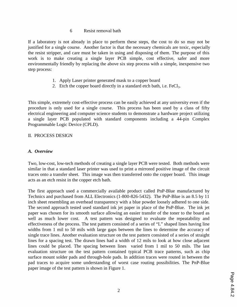
Two, low-cost, low-tech methods of creating a single layer PCB were tested. Both methods weresimilar in that a standard laser printer was used to print a mirrored positive image of the circuittraces onto a transfer sheet. This image was then transferred onto the copper board. This imageacts as an etch resist in the copper etch bath.
The first approach used a commercially available product called PnP-Blue manufactured byTechnics and purchased from ALL Electronics (1-800-826-5432). The PnP-Blue is an 8.5 by 11inch sheet resembling an overhead transparency with a blue powder loosely adhered to one side.The second approach tested used standard ink jet paper in place of the PnP-Blue. The ink jetpaper was chosen for its smooth surface allowing an easier transfer of the toner to the board aswell as much lower cost. A test pattern was designed to evaluate the repeatability andeffectiveness of the process. The test pattern consisted of a series of “L” shaped lines having linewidths from 1 mil to 50 mils with large gaps between the lines to determine the accuracy ofsingle trace lines. Another evaluation structure on the test pattern consisted of a series of straightlines for a spacing test. The drawn lines had a width of 12 mils to look at how close adjacentlines could be placed. The spacing between lines varied from 1 mil to 50 mils. The lastevaluation structure on the test pattern contained typical PCB trace patterns, such as chipsurface mount solder pads and through-hole pads. In addition traces were routed in between thepad traces to acquire some understanding of worst case routing possibilities. The PnP-Bluepaper image of the test pattern is shown in Figure 1. P
age 4.84.2
3
Fig. 1. PnP-Blue plotter paper test pattern mask after being fed through the laser printer.
B. Procedure
Design the circuit layout using the software of your choice. There are many CAD/CAM PCBprograms available for laying out the circuit. A program used by the majority of the class wasEasyTrax, a freeware program available at [http://www.omnigraph.com/software.html]. Arequirement of the layout software for this process is that it be able to print a mirror image of thecircuit layout.
Once your layout is complete, print the circuit from a laser printer on standard printer paper toverify that all components will fit as designed and that the entire circuit properly fits the printedcircuit board being used. To do this, put the components on the printout and ensure that all pinscan simultaneously make contact. Once you are satisfied that the layout is correct, you are readyto transfer the design onto the copper clad board.
Page 4.84.3
4
First, clean the copper board by scrubbing the surface with a wet ScotchBrite pad or steelwool.This will remove surface oxidation and oil for better adhesion during the transfer process. Thenprint the mirror image of your design onto the PnP-Blue (powder side) or ink jet paper. Youwant the printed image to be as dark as possible without causing smudges on non-trace areas.After printing, cut the image out of the transfer sheet leaving a minimum of 1/4’’ around thecircuit pattern.
You will use a standard household clothes iron to transfer the image from the transfer paper toyour cleaned circuit board. The temperature setting is dependent upon the type of toner used inyour printer. Usually a temperature around 200-225o F will work best. A good place to start iswith a setting in the lower region of the "Steam" settings or about 2/3 of the iron’s maximumsetting. This should be a dry process so do not add water to the iron.
Begin by placing your circuit board, copper side up, onto a piece of wood or similar heatinsulating material. A short stack of paper (10 sheets or so) works well. You want a firmsurface which will not get too hot during ironing. Next, place the transfer sheet with the imagefacing down onto the circuit board and begin ironing, applying the heat in a circular motion.Begin by concentrating on one corner until it adheres to the copper surface. This will help tohold the paper in place while working on other areas. You will begin to see the image of yourdesign through the back of the transfer sheet as you continue to iron. Use this as a guide toensure that you are heating the entire surface evenly, paying special attention to the outer edgesof the board. The entire process could take as little as 45 to 100 seconds but it is recommendedthat you continue to iron for at least 5 minutes. In some cases this improves the chances ofgetting a good transfer at the cost of lower resolution.
After ironing, allow the board and paper to completely cool (10 to 15 minutes). After cooling,carefully remove the film by pulling back the corner 180 degrees and "roll" the film off theboard. You are now ready to etch the board.
Before etching the board, inspect the board for shorts and opens. Shorted traces are most easilycorrected at this stage with a utility knife. Voids (opens) can be corrected by placing scotchtape over the void. The tape will be an effective etch resist.
The copper not masked by the transferred image will be removed by etching in a heated FerricChloride (FeCl3) solution. Before using the Ferric Chloride solution it is important to fullyunderstand the associated health hazards and safety precautions. Read the Material Safety DataSheet (MSDS) and enforcing a few simple rules will help to insure the safety of the students.
• Handle under a fume hood whenever possible.
• Wear rubber gloves and eye protection whenever handling solution.
Page 4.84.4

5
• Ferric Chloride will stain anything that it contacts. You may want to wear anapron or lab coat to protect clothing.
Start by pouring about an inch of Ferric Chloride into a Pyrex tray. Place the tray on the hotplate and bring the solution to the optimal temperature of 40oC. DO NOT exceed thistemperature or excessive fumes may occur. Once you have reached the desired temperature,carefully place the board to be etched into the tray with the copper side of the board facing up.Since the solution will etch substantially faster when agitated you will need to rock the tray fromside to side throughout the process.
The rate at which the board etches is dependent on many factors including the rate of agitation,temperature and the amount of metal in the solution. Therefore, it is impossible to determine anexact etch time. You should expect the process to take from 20 to 50 minutes. When the boardis mostly etched, there may be a few spots with copper remaining. Use a Q-Tip to rub additionalFerric Chloride on these areas. At this point the rubbing action should remove any remainingcopper rather quickly.
Once the etching is complete, rinse the board under running water for several minutes to cleanthe copper board. Inspect the copper traces for opens or shorts. Some shorts can be repairedusing a utility knife while opens can be repaired using jumper wires. The traces will appear darksince they are still covered by the toner and etch resist from the PnP-Blue paper. When usingplotter or ink-jet paper, the toner can easily be removed with acetone or sandpaper. However,acetone does not remove the PnPBlue paper residue. You can use a fine grit sandpaper orsteelwool to remove this residue. A picture of the completed test pattern board after cleaning upthe copper is shown in Fig. 2.
Page 4.84.5

6
Fig. 2. Test pattern PCB after copper etching and resist cleanup.
III. DEMONSTRATION VEHICLES
A. VHDL Based ALU Project
A key benefit of this PCB process in an academic environment is in the affordability of ahardware implementation of a circuit design that would otherwise be accessible to the studentonly through computer simulation. The process was tested in a hardware project assigned toUniversity of Louisville’s Electrical Engineering and Computer Science students enrolled in agraduate level VHDL and programmable logic design course during the summer term of 1998.The course presented students with a hardware-level description of CPLDs and FPGAs andproceeded into the use of VHDL software to program these devices. The culmination of thecourse was a hardware project based on the design of a 4-bit microprocessor using VHDL. Thestudents were tasked with synthesizing the ALU portion of the microprocessor using abehavioral level VHDL description of the circuit. The project then required the students to P
age 4.84.6

7
implement and verify the design in hardware by utilizing the board fabrication process and a 44-pin surface mount PLCC CPLD.
In order to make the project more manageable in the constraints of available time and hardware,the design was reduced to a 3-bit ALU without loss of instructive benefit. The inputs to theALU were two 3-bit binary words, R and S, and a 3-bit binary ALU instruction selection. Table1 lists the ALU instruction set. The output was to be displayed on two seven-segment LEDs indecimal form.
Table 1: Instruction set for the 3-bit ALU design.
SelectionWord
Function
000 S – R001 R – S010 R + S011 R AND S100 R OR S101 R XOR S110 (NOTR)
AND S111 (NOT S)
AND R
The text used for the course [2], included WARP, a VHDL compiler written by CypressSemiconductor that runs on a PC. Capabilities include compilation, simulation, timing analysis,JEDEC file generation. and placing and routing. A 44-pin Cypress CY7C372I CPLD waschosen to implement the ALU. It has 64 macrocells with the ability to create up 6192 productterms. Figure 3 shows a schematic of the hardware that was populated on the board.
Page 4.84.7

8
Figure 3. Schematic of the CPLD-ALU demonstration PCB.
Nine DIP switches were used to generate the three 3-bit input words: R, S, and the instructionselection. A bank of nine 15kΩ resistors was used to pull the inputs to the CPLD high when theDIP switches are open. The CPLD outputs, capable of driving the LED segments directly, wereconnected through 680Ω resistors to the LEDs. Additionally, a 10-pin header was utilized toconnect the In-System-Reprogrammable (ISR) programming cable from the PC to the board.
The ALU was coded in VHDL using WARP software and simulated in NOVA, the simulationpackage accompanying WARP. Successful compilation of the VHDL code resulted in thegeneration of a JEDEC file which was then utilized by ISR programming software. To programthe CPLD, the ISR programming cable was connected from the parallel port of the PC to theprogramming header on the board, and the ISR software was invoked to implement the designbased upon the JEDEC file.
The project provided the students with a “hands-on” design experience that incorporated layoutdesign, board fabrication, component selection, board soldering, VHDL design, debugging andtesting. Student groups of two were required to individually design and fabricate a single layerprinted circuit board to meet project specification. The teaming arrangement is also important tohelp prepare the students for teamwork environment of industry. Components were then
Page 4.84.8

9
soldered onto the board in a surface mount fashion, eliminating the need for drilling holes. Somestudents choose to use 100 mil pitch through-hole components to make the soldering easier byavoiding the standard 50 mil pitch of surface mount components. The board was then tested forcorrect operation using a very simple VHDL test program to turn on the LEDs when a DIPswitch was activated. Successively, the 3-bit ALU was written and programmed into the CPLD.A demonstration of the correct operation was required. A picture of the final fabricated andtested board is shown in Fig. 4
Fig. 4. Picture of the final ALU test board without the CPLD in the socket.
B. Cellular Band Power Amplifier with Microstrip Matching Project
The academic environment benefit of affordability and student accessibility is extended topractical applications with its high repeatability. Since this process yields predictable,consistent results, it can be used for processes which require specific trace widths and shapes.The process was tested in a hardware project assigned to University of Louisville’s ElectricalEngineering students enrolled in a graduate level Microwave Engineering course during the fallterm of 1998. The course presented students with a hardware-level description of microwavefundamentals and proceeded into the use of the Smith Chart and Microwave Design software todesign microwave microstrip matching networks. The culmination of the course was a hardwareproject based on the design of cellular band power amplifier. The students were tasked withdesigning a power amplifier for maximum gain in the 950 MHz Cellular phone band includingmicrostrip matching networks. The project then required the students to implement and verifythe design in hardware by utilizing the board fabrication process and a microwave powertransistor.
Page 4.84.9

10
In order to make the project more manageable in the constraints of available time and hardware,the design was reduced to matching only - the biasing would be done off board using standardbias T’s.
The software Libra was used during the course. The majority of the students used a hybriddesign technique to design the matching networks using a Smith chart and hand calculations toobtain a unilateral approximate design which minimized S11 and S22. Libra was then utilizedto check the design and refine the microstrip dimensions utilizing bilateral design techniquesincluding the use of S12 and S21. Figure 5 shows a schematic of the design that wasconstructed on the board.
Figure 5. Schematic of Cellular Band Power Amplifier Design.
The project provided the students with a “hands-on” RF experience that incorporated DC circuitanalysis, RF circuit and layout design, board fabrication, and RF measurement techniques.Student groups of two were required to individually design and fabricate a double layer printedcircuit board to meet project specification. The teaming arrangement is also important to helpprepare the students for teamwork environment of industry. The microwave transistor andconnectors were then soldered onto the board. Unlike the VHDL project, it was necessary to payclose attention to soldering techniques, ensuring good, low inductance soldering joints. Theboard was then tested for correct operation using a simple test setup which measured the gain atdifferent frequencies and power levels. A contest was held for the maximum gain and the course
Page 4.84.10
11
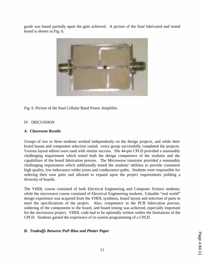
grade was based partially upon the gain achieved. A picture of the final fabricated and testedboard is shown in Fig. 6.
Fig. 6. Picture of the final Cellular Band Power Amplifier.
IV. DISCUSSION
A. Classroom Results
Groups of two or three students worked independently on the design projects, and while theirboard layout and component selection varied, every group successfully completed the projects.Various layout editors were used with similar success. The 44-pin CPLD provided a reasonablychallenging requirement which tested both the design competence of the students and thecapabilities of the board fabrication process. The Microwave transistor provided a reasonablychallenging requirement which additionally tested the students’ abilities to provide consistenthigh quality, low inductance solder joints and conductance paths. Students were responsible forordering their own parts and allowed to expand upon the project requirements yielding adiversity of boards.
The VHDL course consisted of both Electrical Engineering and Computer Science students,while the microwave course consisted of Electrical Engineering students. Valuable “real world”design experience was acquired from the VHDL synthesis, board layout and selection of parts tomeet the specifications of the project. Also, competence in the PCB fabrication process,soldering of the components to the board, and board testing was achieved, especially importantfor the microwave project. VHDL code had to be optimally written within the limitations of theCPLD. Students gained the experience of in-system programming of a CPLD.
B. Tradeoffs Between PnP-Blue and Plotter Paper Page 4.84.11
12
The above process works when using both PnP-Blue and standard ink jet paper. Each methodhas advantages and disadvantages over the other.
The PnP-Blue paper provided for an easier transfer of the image to the copper board. The bluepowder acts as a release allowing the toner to transfer more easily. Using this method, 75% ofthe boards transferred correctly on the first attempt. When using the ink jet paper, a goodtransfer was achieved 33% of the time.
A minor advantage was the shorter ironing times realized when using the PnP paper. Thetransfer could be completed in less then 100 seconds using this method, while ink jet paperrequired ironing times closer to 5 minutes.
The advantages of the ink jet paper are reduced cost, wider availability, and smaller featuresizes. While the PnP paper cost $2.39 per page, the ink jet paper cost approximately 10 centsper page. Even considering that several attempts may have to be made to achieve a goodtransfer, there is still a considerable cost savings. Also, the ink jet paper is more readilyavailable from local sources. Smaller feature sizes were achieved with the ink jet paper. PnP-Blue yielded traces of 15 mils, while ink jet paper yielded traces of 4 mils using a 300 dpi laserprinter. The reason for this is that the blue powder tended to spread out during the ironingprocess.
V. CONCLUSIONS
This PCB fabrication process presented above has the following advantages over traditionalmethods:
• Fewer wet processes.• Lower capital and production costs.• Faster turnaround.• Simple process available to the student.
The process combines affordability and quality with state-of-the art trace widths and spacings assmall as 4 mils using only a 300 dpi laser printer. This results in approximately 1.2 printed dotsper 4 mil line. It is hypothesized that a 1200 dpi laser printer should be able to print reproduciblelines down to widths of 1 mil. This single layer approach can also be applied to two-sidedboards in a straightforward manner. The most critical step using a two-sided board is thealignment of the masks prior to iron transfer. Hence for a reasonable yield it is imperative togive excessive tolerance to the through-hole dimensions, so alignment becomes less critical.
This PCB process has a wide range of applications to a variety of students. This simplistic PCBfabrication process provides students with a fast, easy, and inexpensive source of PCBs that isintrinsically safer for the students to handle over previous processes. Furthermore this process ismuch more environmentally friendly by all-together avoiding toxic resist strippers. The processis extremely useful for courses in which a hardware project is required. For example, this process P
age 4.84.12

13
allowed students learning VHDL to actually see their software design of a 3-bit ALU come tolife using this PCB process with a programmable logic device.
REFERENCES:
[1] R. Marrs, “Trends in IC Packaging and Advanced Assembly”, Electronic Packaging andProduction, pp. 26 – 32, July 1998.
[2] K. Skahill, “VHDL for Programmable Logic”, Addison-Wesley, New York, 1996.
Jerry Branson: Jerry Branson is currently a doctoral student in the Computer Science andEngineering (CSE) Ph.D. program at the University of Louisville. He received his B.S.E.E. in1986 and MEng. in 1987 from the University of Louisville Electrical Engineering Department.Before entering the CSE program, he spent twelve years working as a design engineer includingfour years in Japan and taught in the Mathematics and Science Department at the Yokosuka,Japan campus of the University of Maryland.
John Naber: Dr. Naber received his Ph.D. degree from Virginia Polytechnic Institute in 1992.He received his B.S. and M.Eng. degree's from the University of Louisville in 1983 and 1985respectively. He currently is an Assistant Professor in the Electrical Engineering department atthe University of Louisville. He has eleven years of integrated circuit design and projectmanagement experience with General Electric and ITT. Dr. Naber has designed numerousdigital, analog and RF/microwave integrated circuits using both silicon and GaAs. He has over20 professional publications, is co-writer of “Gallium Arsenide IC Applications Handbook” byAcademic Press and has three patents issued. Dr. Naber is a Senior Member of the IEEE and amember of Tau Beta Pi.
Page 4.84.13


![w À ] 3D-printed Drugs: A Fabrication of Pharmaceuticals](https://img.dokumen.tips/doc/110x75/616a05b511a7b741a34df3cd/w-3d-printed-drugs-a-fabrication-of-pharmaceuticals-.jpg)
