Embed Size (px)
Citation preview
An Optical Voltage Sensor Based onPiezoelectric Thin Film for Grid Applications
JORDAN L. EDMUNDS,1,* SONER SONMEZOGLU,1,** JULIENMARTENS,2 ALEXANDRA VON MEIER,1 MICHEL M. MAHARBIZ,1,3,4
1Department of Electrical Engineering and Computer Sciences, University of California, Berkeley,Berkeley, CA 94704, USA2Department of Microsystems Engineering (IMTEK), Laboratory for Biomedical Microtechnology,University of Freiburg, Freiburg, Germany3Department of Bioengineering, University of California, Berkeley, Berkeley, CA 94704, USA4Chan Zuckerberg Biohub, San Francisco, CA 94158, USA*[email protected]**[email protected]
Abstract: Continuous monitoring of voltages ranging from tens to hundreds of kV overenvironmental conditions, such as temperature, is of great interest in power grid applications.This is typically done via instrument transformers. These transformers, although accurate androbust to environmental conditions, are bulky and expensive, limiting their use in microgridsand distributed sensing applications. Here, we present a millimeter-sized optical voltage sensorbased on piezoelectric aluminum nitride (AlN) thin film for continuous measurements of ACvoltages <350𝑘𝑉𝑟𝑚𝑠 (via capacitive division) that avoids the drawbacks of existing voltage-sensingtransformers. This sensor operated with 110`𝑊 incident optical power from a low-cost LEDachieved a resolution of 170𝑚𝑉𝑟𝑚𝑠 in a 5kHz bandwidth, a measurement inaccuracy of 0.04% dueto sensor nonlinearity, and a gain deviation of +/-0.2% over the temperature range of ~20-60𝐶.The sensor has a breakdown voltage of 100V, and its lifetime can meet or exceed that of instrumenttransformers when operated at voltages <42𝑉𝑟𝑚𝑠. We believe that our sensor has the potentialto reduce the cost of grid monitoring, providing a path towards more distributed sensing andcontrol of the grid.
© 2021 Optical Society of America under the terms of the OSA Open Access Publishing Agreement
1. Introduction
Safe, accurate, and economical measurement of time-varying voltages in electric power systemsis a significant challenge. The standard solution to this challenge is the instrument transformer,which steps down a high voltage (~1kV+) to an appropriate level (typically <100V) and isolates thestepped-down voltage, allowing safe measurement using conventional electronics. However, thesetransformers are bulky and expensive and sometimes explode (~3% of all installed instrumenttransformers [1]). Optical methods for direct measurement of high voltages have gained attentionsince the early 1980s [2], mainly due to the high available bandwidth (~GHz), intrinsic electricalisolation, and the potential for low cost and remote monitoring. Initial optical voltage sensorsconsisted of long (several meters) optical fiber wrapped around a piezoelectric material [2]. Inthese sensors, when the piezo material was excited by a voltage, it grew or shrank proportional tothe applied voltage, changing the fiber optical path length; the resulting change in the opticalpath length was measured using interferometry to infer the voltage amplitude. More recentoptical methods include coupling piezoelectric material to the resonant frequency of Bragg fibergratings [3–5]. However, the sensors based on the above optical methods are inaccurate due totheir nonlinearities [5] or temperature sensitivity [4–6]. Closed-loop compensation methods wereused to improve the accuracy of such sensors [7, 8], but these methods reduce system reliabilityand increase system complexity, electrical hazards, and cost.
arX
iv:2
108.
0594
2v1
[ph
ysic
s.ap
p-ph
] 2
3 Ju
l 202
1

Fundamentally, output nonlinearity and temperature dependence increase with an increasingquality factor (𝑄) of the interferometric- or optical cavity-based sensor, where Q is defined as theratio of the energy stored in the cavity to the energy dissipated per oscillation period. Therefore,a low-𝑄 sensor is desirable to minimize nonlinearity and temperature dependence. However,low-𝑄 sensors suffer from low sensitivity, resulting in a low signal-to-noise ratio (SNR) and poorperformance. In practice, the SNR, and hence performance, can be improved independently ofthe sensor sensitivity by increasing the incident optical power (𝑃𝑖𝑛) or reducing the operatingbandwidth (𝐵𝑊). This makes performance comparison of different optical voltage sensorsdifficult; they must be operated with the same 𝑃𝑖𝑛 and 𝐵𝑊 for a fair comparison.
Given this, a 𝑃𝑖𝑛 and 𝐵𝑊 independent figure of merit (FoM) is required to quantify the noiseperformance of optical voltage sensors. We propose such a metric, the energy per quanta (𝐸𝑄),which depends only on the sensor properties and dynamic input range. This metric extends thepower efficiency factor used in analog circuit design [9] and the energy per conversion-level ofanalog-to-digital-converters [10, 11]. Lower 𝑄-factors yield less sensitive sensors and a higher𝐸𝑄 (𝐸𝑄 ∝ 1/𝑄2).
In this work, we propose trading off 𝐸𝑄 for temperature insensitivity and reduced harmonicdistortion, and explore the limits of this approach. To this end, we demonstrate a low-𝑄 resonantoptical cavity-based voltage sensor based on a piezoelectric AlN thin film that transduces avoltage applied across the piezo terminals into a change in the resonant frequency of the cavity.This sensor can be batch fabricated with high yield and low cost (<$1), which makes it uniquelywell-suited to reduce the cost of grid voltage measurement.
2. Optical voltage sensor design and sensor fabrication
2.1. Operating principle and fabrication process of the sensor
Fig. 1 shows the operating principle of the proposed optical voltage sensor (OVS) based onchanges in the measured reflectance of a resonant cavity, whose thickness varies with appliedvoltage. The resonant cavity is formed by an AlN thin film sandwiched between the top indiumtin oxide (ITO) electrode and the bottom silicon (Si) substrate. During operation, the sensor isilluminated by a light source with an incident optical power (𝑃𝑖𝑛) at a fixed wavelength (_𝑖𝑛)near the resonance wavelength of the cavity (_𝑟 ). Some fraction of 𝑃𝑖𝑛 is reflected from thecavity, with the remainder dissipated in or transmitted through the cavity, as seen in Fig. 1. Here,the intensity of reflected light (𝑃𝑟=𝑃𝑖𝑛×𝑅, where 𝑅 is the cavity reflectance) is measured bya photodetector to detect the amplitude of an input voltage (𝑉𝑖𝑛) applied across the cavity. 𝑃𝑟
depends on 𝑉𝑖𝑛 through 𝑅 as 𝑉𝑖𝑛 generates an electric field in the cavity that changes the AlNfilm thickness [12] and refractive index [13] and hence results in a shift in resonant wavelengthΔ_ = _𝑟 − _𝑟0, where _𝑟0 is the resonant wavelength at 𝑉𝑖𝑛 = 0. The resulting _𝑟 shift leads to achange in the reflectance (Δ𝑅 =𝑅-𝑅0, where 𝑅0 is the reflectance at 𝑉𝑖𝑛=0). The Δ𝑅 value at aknown 𝑉𝑖𝑛 can be calculated using the following expression (see supplementary material for thederivation of (1)):
Δ𝑅 = 𝛽𝑉𝑖𝑛 (1)
𝛽 =3√
34
𝑅𝑚𝑎𝑥𝑄
𝑡
(𝑑33 + 1
2𝑛2
0𝑟33
)(2)
where 𝑅𝑚𝑎𝑥 is the amplitude of the resonant dip (always <1), 𝑄 and 𝑡 are the quality factorand thickness of the cavity, 𝑑33 is the thickness mode piezoelectric strain coefficient, 𝑛0 isthe (unperturbed) refractive index of the AlN thin film, and 𝑟33 is the Pockels coefficient(which relates the refractive index to the applied electric field). This equation is valid near

Pin R0·Pin
0V
Pin (R0+ΔR)·Pin
ΔⲖ
ΔR
Ⲗin Ⲗ
R
R0
Top Electrode
Substrate
AlN
Fig. 1. Sensor principle of operation. During operation, the sensor is illuminated byan incident optical power 𝑃𝑖𝑛 at a wavelength _𝑖𝑛 (that is, the steepest point of thereflectance curve) offset from the resonant wavelength _𝑟 . An input voltage 𝑉𝑖𝑛 appliedacross the cavity results in a shift in the resonant spectrum from the solid (unperturbed)to the dashed (perturbed) spectrum, causing a change in the reflectance Δ𝑅 at _𝑖𝑛. Theresulting Δ𝑅 change alters the amount of reflected light power (𝑃𝑟=𝑅0+Δ𝑅) · 𝑃𝑖𝑛) thatis measured to determine the 𝑉𝑖𝑛.
_𝑖𝑛 ≈ ±_𝑟 + 1/√3 · 𝐹𝑊𝐻𝑀; this corresponds to the steepest point on the reflectance curve,where 𝐹𝑊𝐻𝑀 is the full-width-half max of the resonant dip.
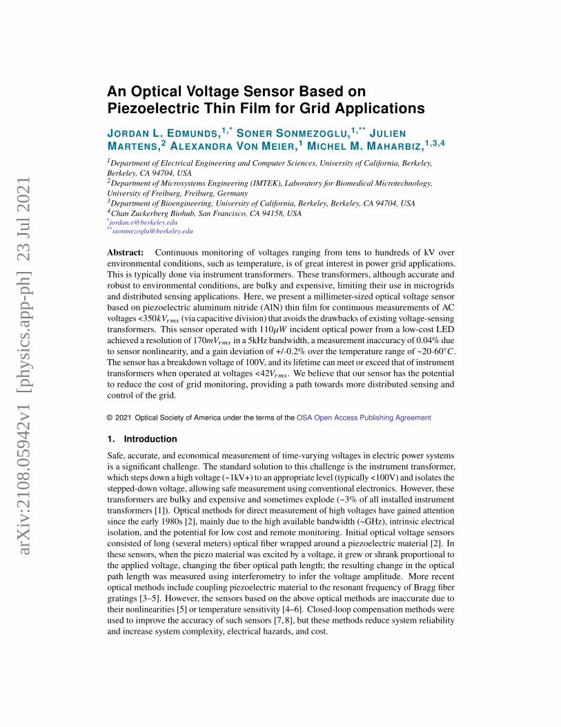
Fig. 2(a) shows the OVS fabrication process. All lithography was done in a DUV stepper(ASML), on a 150mm-thick silicon (Si) wafer. We first sputtered a ~300nm-thick layer ofbackside aluminum (Al), and then annealed the wafer at 300°C for 15min in atmosphere to createbackside ohmic contacts that serves as the bottom electrode. Next, we deposited a 300nm-thickaluminum nitride (AlN) film (endeavor AT) and a 20nm-thick indium tin oxide (ITO) film toserve as the transparent top electrode. Finally, we patterned the top ITO contacts to form 2mmdiameter devices and evaporated 20nm titanium (Ti)/300nm Al to form bond pads. The fabricated10×10𝑚𝑚2 sensor die was attached with conductive silver epoxy and wire-bonded to a printedcircuit board (PCB). An optical micrograph of the 2mm diameter sensor on its PCB are shownin Fig. 2(b) The die size was designed to be larger than the actual device size to facilitate easyhandling. See the supplementary information for specific process details.
Optical shot noise sets a hard limit on OVS performance. The performance of opticaldetection systems is bounded by shot noise received at the photodetector. For a shot-noiselimited OVS system, the system SNR is proportional to the input optical power, which isgiven by 𝐼2
𝑝𝑑/𝐼2𝑛𝑜𝑖𝑠𝑒 = Δ𝐼2
𝑝𝑑/(2𝑞(𝐼𝑝𝑑 + Δ𝐼𝑝𝑑) · 𝐵𝑊), where 𝑞 is the electron charge, 𝐼𝑝𝑑 is thelight-induced photocurrent on the photodetector, Δ𝐼𝑝𝑑 is the change in the rms photocurrentinduced by an applied input voltage (𝑉𝑖𝑛), and 𝐵𝑊 is the system bandwidth. The SNR can alsobe expressed in terms of an an incident light power (𝑃𝑖𝑛), the average device reflectance (〈𝑅〉),and an rms modulation depth (Δ𝑅, that is, the change in 𝑅 due to an applied 𝑉𝑖𝑛) in the followingform, using 𝐼𝑝𝑑 = 𝑃𝑖𝑛 · < · 𝑅:

1
2
3
4
5
ITO Al
AlN Si
a b
Fig. 2. (a) Sensor fabrication process. 1. Backside Al (~300nm) sputter and anneal at300°C for 15 minutes 2. Frontside AlN (300nm) reactive sputter 3. Topside ITO (20nm)sputter 4. Lithographic patterning, ion milling of device mesas 5. Bond pad patterningTi/Al (20nm/300nm) evaporation and lift-off. (b) Photograph of the fabricated sensordie on a PCB, and (inset) optical top-view micrograph of the sensor.
𝑆𝑁𝑅 ≈ 𝑃𝑖𝑛 · < · Δ𝑅2
2𝑞 · 〈𝑅〉 · 𝐵𝑊 (3)
where < is the responsivity of the photodetector. Eq. 3 reveals the system SNR depends notonly on 𝑉𝑖𝑛 through 𝑅 but also 𝑃𝑖𝑛 and 𝐵𝑊 , consistent with the expectation that larger 𝑃𝑖𝑛 andsmaller 𝐵𝑊 provide a better SNR in the optical voltage sensing system. However, optical sourcescan only supply a limited amount of power, and system-level requirements could potentially limitthe maximum 𝑃𝑖𝑛 and the minimum 𝐵𝑊 in the system.
The input-referred energy per quanta (𝐸𝑄) allows quantitative configuration-independentsensor comparison. Since the best choices for 𝑃𝑖𝑛 and 𝐵𝑊 will vary by application, it is usefulto introduce a metric that normalizes SNR to 𝑃𝑖𝑛 and 𝐵𝑊 . This would allow a rigorous noiseperformance comparison between optical voltage sensors, independent of the sensor’s particularoperating 𝑃𝑖𝑛 or 𝐵𝑊 . In digital systems (optical and otherwise), the energy per bit has become aubiquitous metric of device performance [14]. Here, we propose an alternative metric for analogsystems, the energy per quanta (𝐸𝑄), defined as:
𝐸𝑄 ≡ 𝑃𝑖𝑛
SNR · 𝐵𝑊 (4)
This metric demonstrates how efficiently 𝑃𝑖𝑛 is used, and can be interpreted as a cost paidin energy to achieve a desirable SNR. For a shot-noise limited system, 𝐸𝑄 can be derived,independent of 𝑃𝑖𝑛 and 𝐵𝑊 , by inserting Eq. 3 into Eq. 4:
𝐸𝑄,𝑚𝑖𝑛 ≈ 𝑞 · 〈𝑅〉< · Δ𝑅2 (5)
The form of this equation makes it clear that reducing the average cavity reflectance 〈𝑅〉 at theexpense of modulation depth Δ𝑅 at the operating wavelength can improve the noise performanceof the system, as observed in [15]. 𝐸𝑄 is bounded from below by the incident photon energycaptured by the photodetector.
2.2. Optical voltage sensor (OVS) design
We designed our OVS to measure grid-level AC voltages in the range of tens to hundreds ofkVs via capacitive division. The system bandwidth (𝐵𝑊) was set to 5kHz, satisfying the 𝐵𝑊requirement of most grid applications, including inverter-based solar [16]. To minimize sensornonlinearity and temperature sensitivity, we chose to deliberately design the sensor to have a high𝐸𝑄, as 𝑑𝛽/𝑑𝑇 ∝ 1/𝐸𝑄 and 𝑑𝛽/𝑑𝑉𝑖𝑛 ∝ 1/𝐸𝑄 (where 𝛽 is the sensor gain, shown in Eq. 2, and𝛽 = 𝛽(𝑉𝑖𝑛, 𝑇)/𝛽(0, 0) is the normalized gain). To achieve a high 𝐸𝑄, we minimized the sensor𝑄-factor by designing the cavity as thin as possible (𝐿 = 300𝑛𝑚) and excluding mirrors (otherthan the material interfaces).
Furthermore, most previous sensors use lead zirconate titanate (PZT) as a piezoelectricmaterial to form the resonant cavity as it provides a large piezoelectric strain coefficient(𝑑33 ≈ 500𝑝𝑚/𝑉 [17]). However, the PZT 𝑑33 is extremely temperature sensitive (~20% over100𝐶 ) [18]. Therefore, here we elected to use aluminum nitride (AlN) for our sensor to furtherminimize the sensor temperature dependence as its 𝑑33 is independent of temperature [19, 20].
3. Experiment results
The optical voltage sensor (OVS) was characterized using the setup shown in Fig. 3, where weused an LED (Thorlabs, M970F3) with a peak intensity at ~970𝑛𝑚 (±10𝑛𝑚) and a mean intensityat ~950nm. The light from the LED is fiber-coupled to collimating lens L1, beam-splitter BS1,focusing lens L2, focusing lens L3, 850nm long-pass filter F1 (Thorlabs FELH0850) and Siphotodiode PD (Thorlabs, SM05PD2B). The PD (Thorlabs, SM05PD2B) was connected toa transimpedance amplifier (TIA) with a 1MΩ feedback resistance to convert a light-inducedphotocurrent on the PD to a voltage. The resulting voltage was digitized by an analog-to-digitalconverter (ADC) (NI myDAQ; National Instruments) with a 10kHz sampling rate and then sentto a computer through a serial link for data storage and further analysis.
Light Source (LED)
PD
L1
L3 L2F1
BS1
Device
ADC
TIA
PersonalComputer
Fig. 3. Sensor characterization setup. Light is emitted by an LED source, focused ontodevice, imaged onto a photodiode, and measured with a TIA. The TIA output is sent tothe ADC to be recorded in the computer.
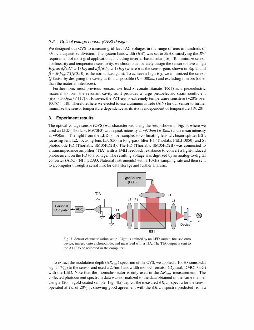
To extract the modulation depth (Δ𝑅𝑟𝑚𝑠) spectrum of the OVS, we applied a 105Hz sinusoidalsignal (𝑉𝑖𝑛) to the sensor and used a 2.4nm bandwidth monochromator (Dynasil, DMC1-05G)with the LED. Note that the monochromator is only used in the Δ𝑅𝑟𝑚𝑠 measurement. Thecollected photocurrent spectrum data was normalized to the data obtained in the same mannerusing a 120nm gold-coated sample. Fig. 4(a) depicts the measured Δ𝑅𝑟𝑚𝑠 spectra for the sensoroperated at 𝑉𝑖𝑛 of 20𝑉𝑝𝑝, showing good agreement with the Δ𝑅𝑟𝑚𝑠 spectra predicted from a

0 2 4 6Vin (Vrms)
0.0
2.5
5.0
7.5
10.0
12.5
15.0
Pho
tocu
rren
t (nArms)
R2 = 0.999997Iout = 2.09×Vin+ 0.009
Linear Fit
Measured
900 950 1000Wavelength (nm)
0
0.5× 10 4
1.0× 10 4
1.5× 10 4
2.0× 10 4
Rrms
Theory
Measured
100 300 500Frequency (Hz)
80
60
40
20
0
Nor
mal
ized
Pow
er(d
B)
1st harmonic
2nd harmonic
a
c
b
Fig. 4. (a) Measured and predicted modulation depth spectra of the sensor operatedwith an input voltage (𝑉𝑖𝑛) of 20𝑉𝑝𝑝 (Dataset 1). (b) Output photocurrent versus𝑉𝑖𝑛 applied to the sensor (Dataset 2). (c) Power spectral density of the sensor output(averaged 500 times, the duration of each measurement was 10s), normalized withrespect to the first harmonic amplitude (Dataset 3).
thin-film Fresnel equation model (supplementary materials) using the parameters provided inSupplementary Table S1. The difference in the measured and predicted spectra can be mainlyattributed to the Si substrate becoming increasingly transparent at longer wavelengths, causingthe transmitted light through the AlN layer (subsequently reflected by the Si/Al interface) topartially cancel the reflected light from the cavity.
The sensor operated with an incident optical power (Pin) of 110`W exhibits a resolutionof 170mVrms in a 5kHz bandwidth with a full scale of 140𝑉𝑟𝑚𝑠 . Fig. 4(b) depicts the outputphotocurrent as a function of 𝑉𝑖𝑛 (105Hz sinusoidal signal) (Dataset 2). The sensor operatedwith 𝑃𝑖𝑛 of 110`𝑊 shows a sensitivity of 2.09nA/V and a noise floor of 5.0𝑝𝐴/√𝐻𝑧, yielding avoltage resolution of 2.4𝑚𝑉/√𝐻𝑧, corresponding to 170𝑚𝑉𝑟𝑚𝑠 in a 5kHz bandwidth. Note thatthe measured noise floor was in excess of the shot noise limit (2.3𝑝𝐴/√𝐻𝑧) by 6.6dB, dominatedby the noise from the LED.
The sensor nonlinearity results in a measurement inaccuracy of only 0.04%. In thenonlinearity test, the sensor was operated with 𝑉𝑖𝑛=20𝑉𝑝𝑝 and 𝑃𝑖𝑛=~110`𝑊 . Fig. 4(c) showsthe normalized power spectral density of the sensor output (Dataset 3). The second harmonicpower (-67.3dB) corresponds to a measurement inaccuracy of 0.04% in the sensor output; thisresult is consistent with the nonlinearity of AlN reported in [21]. The third harmonic is invisiblein the spectrum as its power is below the sensor noise level. The other tones seen in Fig. 4(c) are

25 30 35 40 45 50 55 60Temperature ( C)
0.2
0.1
0.0
0.1
0.2
Gai
n D
evia
tion
(%)
Linear FitMeasured
Fig. 5. Normalized change in sensor gain (Δ𝛽/𝛽) versus temperature. Raw dataavailable in Dataset 4.
the 60Hz interference tone and its numerous harmonics.The sensor output varies only +/-0.2% over a ~40°C temperature range. We measured
the temperature dependence of the sensor gain (𝛽, see Eq. 2). During the measurement, thesensor, operated with a 20𝑉𝑝𝑝, 105Hz sinusoidal signal (𝑉𝑖𝑛), was placed on a 250µm-thickpolyimide heater (Omega) that was controlled using a PID controller (Omega, CSi32) and aK-type thermocouple attached to the sensor die. The measurement result in Fig, 5 showed thatthe sensor gain varies only +/-0.2% in the temperature range of 23-57𝐶, yielding a temperaturesensitivity of ~0.01%/𝐶. We fit the measured (Δ𝛽/𝛽)/Δ𝑇 using a monochromatic Fresnelequation based optical model [22], with the incident wavelength as the fitting parameter. Fromthis model, the incident wavelength was fit to 940nm, which is 10nm lower than the LED’s meanemission wavelength, within the manufacturer’s tolerance. This is about 30nm away from theoptimal operation wavelength of 911nm at which point the error is predicted to be quadratic withtemperature, with a max deviation of less than +/-0.02%.
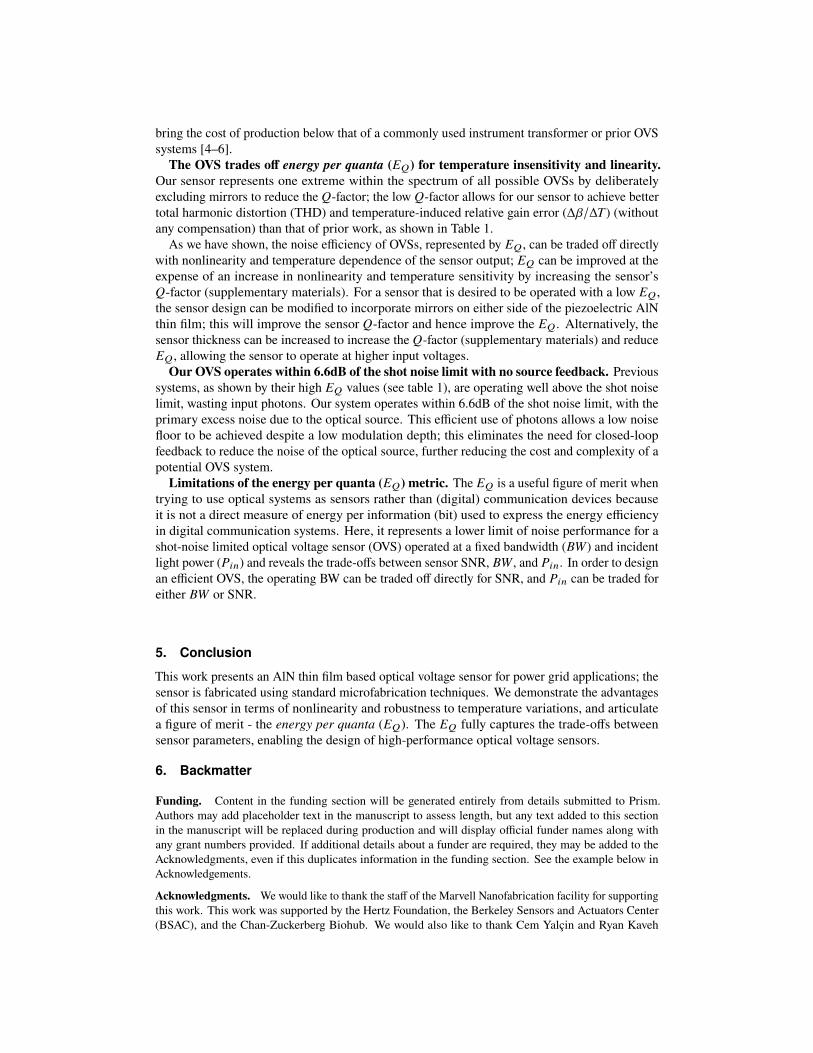
Sensor lifetime can meet or exceed that of instrument transformers. To determine themaximum electric field (𝐸) that could be safely applied to the sensor along with the expectedsensor lifetime, we measured the breakdown charge 𝑄𝑏𝑑 of 8 sensors with low leakage currentsof less than 0.1nA at 10V input voltage (𝑉𝑖𝑛) [23]. During the measurement, we subjected thesesensors to a linear voltage ramp to 43𝑉 , followed by a temperature ramp (~5𝐶/𝑚𝑖𝑛) to 180𝐶,and recorded the current over time until the point of failure. The obtained data were fit to aWeibull distribution [24], whose cumulative distribution function (CDF) is
1 − 𝑒−(𝑄/𝑄0)𝛾 (6)
where 𝛾 is the Weibull slope and 𝑄0 is the characteristic charge. We extracted values of𝛾=0.67 and 𝑄0=379mC (Supplementary figure S2). Combining the extracted Weibull CDF(Supplementary figure S2) with the leakage current at room temperature (Supplementary figureS3), we estimated the likelihood of sensor failure over time at various operating input voltages(see Fig. 6).

0 10 20 30 40Time (yr)
101
100
Failu
re P
roba
bilit
y10V20V30V40V
Fig. 6. Probability of device failure versus time at various DC operating voltages. Dataunderlying curve available in Datasets 6-7
4. Discussion
Monitoring grid-level voltage up to ~350𝑘𝑉𝑟𝑚𝑠 is possible through capacitive division. Sincethe optical voltage sensor (OVS) is based on a 300nm AlN thin film, a large device capacitance(>1nF) is possible despite the small sensor size (2mm diameter) and relatively low-permittivitydielectric (𝜖𝑟=9.5). We measured the sensor impedance using an HP2484A LCR meter from10kHz-500kHz (Supplementary figure S4, Dataset 5), and extracted the device capacitance(C=0.997nF) and resistance (R=389Ω) from fitting the measured data to a series R/C model. Thisrelatively high capacitance allows for off-the-shelf capacitors (>~1pF) to be used for capacitivedivision and hence to facilitate measuring high voltages in the order of tens to hundreds ofkVs. Fabricating the device on an insulating substrate would also enable capacitive division.For example, a quartz substrate (𝜖𝑟=4.5 [25]) with a typical thickness of 675`𝑚 can be usedto fabricate the sensor and form a capacitive divider on the same die; the quartz capacitancedensity (0.06𝑝𝐹/𝑚𝑚2) is much lower than the AlN film capacitance density (280𝑝𝐹/𝑚𝑚2) andallows approximately 5000:1 capacitive division for the same size sensor and capacitor. Witha breakdown voltage of 100𝑉 , this could enable voltage sensing up to 350𝑘𝑉𝑟𝑚𝑠, but one canchoose to operate the sensor with voltages < 350𝑘𝑉𝑟𝑚𝑠 to extend the sensor operational lifetime.
The low-cost OVS system can be built using our device and inexpensive optical compo-nents. To our knowledge, we present the first OVS that uses an LED for operation, rather thana specialized light source such as an amplified spontaneous emission source (ASE) [4, 5] orsuperluminescent LED (SLED) [6] (see Table 1). Our low 𝑄-factor device enables using aconventional broadband light source LED without the need of an optical filter, which allowssensor operation at higher powers near baseband with lower noise floors. This is because LEDsdo not suffer from the same low-frequency excess noise that other narrowband light sources, suchas lasers, do and can get very close to the shot noise limit [26]. Additionally, the sensor can beinterrogated at an angle or in a transmissive configuration; this would allow input and outputfibers to be coupled directly to the sensor, without the necessity of using optical circulators orbeamsplitters. Since this device is a relatively large size (mm-scale) it does not require precisealignment. Taken together, these properties can enable building an optical voltage sensing systembased on our sensor and inexpensive optical components (LEDs and optical fibers), which could
bring the cost of production below that of a commonly used instrument transformer or prior OVSsystems [4–6].
The OVS trades off energy per quanta (𝐸𝑄) for temperature insensitivity and linearity.Our sensor represents one extreme within the spectrum of all possible OVSs by deliberatelyexcluding mirrors to reduce the 𝑄-factor; the low 𝑄-factor allows for our sensor to achieve bettertotal harmonic distortion (THD) and temperature-induced relative gain error (Δ𝛽/Δ𝑇) (withoutany compensation) than that of prior work, as shown in Table 1.
As we have shown, the noise efficiency of OVSs, represented by 𝐸𝑄, can be traded off directlywith nonlinearity and temperature dependence of the sensor output; 𝐸𝑄 can be improved at theexpense of an increase in nonlinearity and temperature sensitivity by increasing the sensor’s𝑄-factor (supplementary materials). For a sensor that is desired to be operated with a low 𝐸𝑄,the sensor design can be modified to incorporate mirrors on either side of the piezoelectric AlNthin film; this will improve the sensor 𝑄-factor and hence improve the 𝐸𝑄. Alternatively, thesensor thickness can be increased to increase the 𝑄-factor (supplementary materials) and reduce𝐸𝑄, allowing the sensor to operate at higher input voltages.
Our OVS operates within 6.6dB of the shot noise limit with no source feedback. Previoussystems, as shown by their high 𝐸𝑄 values (see table 1), are operating well above the shot noiselimit, wasting input photons. Our system operates within 6.6dB of the shot noise limit, with theprimary excess noise due to the optical source. This efficient use of photons allows a low noisefloor to be achieved despite a low modulation depth; this eliminates the need for closed-loopfeedback to reduce the noise of the optical source, further reducing the cost and complexity of apotential OVS system.
Limitations of the energy per quanta (𝐸𝑄) metric. The 𝐸𝑄 is a useful figure of merit whentrying to use optical systems as sensors rather than (digital) communication devices becauseit is not a direct measure of energy per information (bit) used to express the energy efficiencyin digital communication systems. Here, it represents a lower limit of noise performance for ashot-noise limited optical voltage sensor (OVS) operated at a fixed bandwidth (𝐵𝑊) and incidentlight power (𝑃𝑖𝑛) and reveals the trade-offs between sensor SNR, 𝐵𝑊 , and 𝑃𝑖𝑛. In order to designan efficient OVS, the operating BW can be traded off directly for SNR, and 𝑃𝑖𝑛 can be traded foreither 𝐵𝑊 or SNR.
5. Conclusion
This work presents an AlN thin film based optical voltage sensor for power grid applications; thesensor is fabricated using standard microfabrication techniques. We demonstrate the advantagesof this sensor in terms of nonlinearity and robustness to temperature variations, and articulatea figure of merit - the energy per quanta (𝐸𝑄). The 𝐸𝑄 fully captures the trade-offs betweensensor parameters, enabling the design of high-performance optical voltage sensors.
6. Backmatter
Funding. Content in the funding section will be generated entirely from details submitted to Prism.Authors may add placeholder text in the manuscript to assess length, but any text added to this sectionin the manuscript will be replaced during production and will display official funder names along withany grant numbers provided. If additional details about a funder are required, they may be added to theAcknowledgments, even if this duplicates information in the funding section. See the example below inAcknowledgements.
Acknowledgments. We would like to thank the staff of the Marvell Nanofabrication facility for supportingthis work. This work was supported by the Hertz Foundation, the Berkeley Sensors and Actuators Center(BSAC), and the Chan-Zuckerberg Biohub. We would also like to thank Cem Yalçin and Ryan Kaveh

Table 1. Comparison of state-of-the-art optical voltage sensors.
[4] [5] [6] This work
Architecture Dual FBG FBG FBG Thin-film
Light Source Broadband ASE Broadband ASE SLED LED
𝑃𝑖𝑛 ~1mW 25mW𝑐 500`𝑊 𝑓 110`W
𝐵𝑊 20kHz 5kHz 1kHz 5kHz
𝑆𝑁𝑅𝑚𝑎𝑥 21dB 3dB𝑑 54dB 35dB
𝐸𝑄 ~370 2.5`𝐽 1.9𝑝𝐽 13pJ
THD -47dB𝑎 -23dB -51dB -67dB(Δ𝛽/𝛽)Δ𝑇 44%/𝐶𝑏 0.2%/𝐶𝑒 0.2%/𝐶𝑒 0.011%/C
Compensation FBG Thermal screws Bias point tracking None𝑎 Estimated from 𝑉𝑜𝑢𝑡/𝑉𝑖𝑛 transfer function.𝑏 Maximum differential change in gain 𝛽 from 6𝐶 to 8𝐶.𝑐 Input power not specified. Assume maximum power of typical ASE light source (500mW) with aninsertion loss of 13dB, identical to our own.𝑑 Estimated from PSD noise of 0.01V in 16Hz bin and signal (including spectral leakage) of 0.93V across 4bins.𝑒 Estimated from the temperature coefficient of PZT [18], which was not accounted for by the authors.𝑓 Input power not specified. Assume power of typical SLED light source (10mW) with an insertion loss of13dB, identical to our own.FBG: Fiber Bragg GratingΔ𝛽/𝛽: Normalized sensor gain
for their conversations on mixed-signal circuits, and Ryan Rivers for his extensive support on design andfabrication. Michel Maharbiz is a Chan Zuckerberg Investigator.
Disclosures.
The authors declare no conflicts of interest.
Data Availability Statement. Data underlying the results presented in this paper are publicly availableat [27].
Supplemental document. See Supplement 1 for supporting content.
References1. M. Poljak and B. Bojanić, “Method for the reduction of in-service instrument transformer explosions,” Eur. transactions
on electrical power 20, 927–937 (2010).2. T. Yoshino, K. Kurosawa, K. Itoh, and T. Ose, “Fiber-optic fabry-perot interferometer and its sensor applications,”
IEEE Transactions on Microw. Theory Tech. 30, 1612–1621 (1982).3. C. E. Seeley, G. Koste, B. Tran, and T. Dermis, “Packaging and performance of a piezo-optic voltage sensor,” inASME International Mechanical Engineering Congress and Exposition, vol. 42991 (2007), pp. 287–296.
4. Q. Yang, Y. He, S. Sun, M. Luo, and R. Han, “An optical fiber bragg grating and piezoelectric ceramic voltagesensor,” Rev. Sci. Instruments 88, 105005 (2017).
5. M. N. Gonçalves and M. M. Werneck, “A temperature-independent optical voltage transformer based on fbg-pzt for13.8 kv distribution lines,” Measurement 147, 106891 (2019).
6. A. Dante, R. M. Bacurau, A. W. Spengler, E. C. Ferreira, and J. A. S. Dias, “A temperature-independent interrogationtechnique for fbg sensors using monolithic multilayer piezoelectric actuators,” IEEE Transactions on InstrumentationMeas. 65, 2476–2484 (2016).

7. L. Hui, B. Lan, L. Lijing, H. Shuling, F. Xiujuan, and Z. Chunxi, “Tracking algorithm for the gain of the phasemodulator in closed-loop optical voltage sensors,” Opt. & Laser Technol. 47, 214–220 (2013).
8. H. Li, L. Cui, Z. Lin, L. Li, and C. Zhang, “An analysis on the optimization of closed-loop detection method foroptical voltage sensor based on pockels effect,” J. lightwave technology 32, 1006–1013 (2014).
9. R. Muller, S. Gambini, and J. M. Rabaey, “A 0.013𝑚𝑚2, 5`𝑤 , dc-coupled neural signal acquisition ic with 0.5 vsupply,” IEEE J. Solid-State Circuits 47, 232–243 (2011).
10. R. H. Walden, “Analog-to-digital converter technology comparison,” in Proceedings of 1994 IEEE GaAs ICSymposium, (IEEE, 1994), pp. 217–219.
11. R. H. Walden, “Analog-to-digital converter survey and analysis,” IEEE J. on selected areas communications 17,539–550 (1999).
12. C. Lueng, H. L. Chan, C. Surya, and C. Choy, “Piezoelectric coefficient of aluminum nitride and gallium nitride,” J.applied physics 88, 5360–5363 (2000).
13. P. Gräupner, J. Pommier, A. Cachard, and J. Coutaz, “Electro-optical effect in aluminum nitride waveguides,” J.applied physics 71, 4136–4139 (1992).
14. R. S. Tucker, “Green optical communications—part i: Energy limitations in transport,” IEEE J. selected topicsquantum electronics 17, 245–260 (2010).
15. D.-J. Lee and J. F. Whitaker, “Optimization of sideband modulation in optical-heterodyne-downmixed electro-opticsensing,” Appl. optics 48, 1583–1590 (2009).
16. L. Fan, Z. Miao, and M. Zhang, “Subcycle overvoltage dynamics in solar pvs,” IEEE Transactions on Power Deliv.36, 1847–1858 (2020).
17. X.-h. Du, J. Zheng, U. Belegundu, and K. Uchino, “Crystal orientation dependence of piezoelectric properties of leadzirconate titanate near the morphotropic phase boundary,” Appl. physics letters 72, 2421–2423 (1998).
18. F. Li, Z. Xu, X. Wei, and X. Yao, “Determination of temperature dependence of piezoelectric coefficients matrix oflead zirconate titanate ceramics by quasi-static and resonance method,” J. Phys. D: Appl. Phys. 42, 095417 (2009).
19. K. Kano, K. Arakawa, Y. Takeuchi, M. Akiyama, N. Ueno, and N. Kawahara, “Temperature dependence ofpiezoelectric properties of sputtered aln on silicon substrate,” Sensors Actuators A: Phys. 130, 397–402 (2006).
20. C. Rossel, M. Sousa, S. Abel, D. Caimi, A. Suhm, J. Abergel, G. Le Rhun, and E. Defay, “Temperature dependenceof the transverse piezoelectric coefficient of thin films and aging effects,” J. Appl. Phys. 115, 034105 (2014).
21. J. A. Boales, S. Erramilli, and P. Mohanty, “Measurement of nonlinear piezoelectric coefficients using a microme-chanical resonator,” Appl. Phys. Lett. 113, 083501 (2018).
22. E. Hecht and A. Zajac, Optics, vol. 4 (Addison Wesley San Francisco, 2002).23. J. Verweij and J. Klootwijk, “Dielectric breakdown i: A review of oxide breakdown,” Microelectron. J. 27, 611–622
(1996).24. J. I. McCool, Using the Weibull distribution: reliability, modeling, and inference, vol. 950 (John Wiley & Sons,
2012).25. J. Krupka, K. Derzakowski, M. Tobar, J. Hartnett, and R. G. Geyer, “Complex permittivity of some ultralow loss
dielectric crystals at cryogenic temperatures,” Meas. Sci. Technol. 10, 387 (1999).26. S. Rumyantsev, M. Shur, Y. Bilenko, P. Kosterin, and B. Salzberg, “Low frequency noise and long-term stability of
noncoherent light sources,” J. applied physics 96, 966–969 (2004).27. J. Edmunds, M. M. Maharbiz, S. Sonmezoglu, A. von Meier, and J. Martens, “Raw data for "an optical voltage sensor
based on piezoelectric thin film for grid applications",” figshare (2021).

An Optical Voltage Sensor Based onPiezoelectric Thin Film for GridApplications: supplemental document
1. BREAKDOWN FIELD
1 2 3 4field (MV / cm)
102
101
100
-ln(1
-F)
FitMeasured
Fig. S1. Cumulative number of failures vs. applied electric field (Weibull plot). F: CDF of thefailure probability distribution. Raw data available in Dataset 5.
The overall Weibull slope γ for the breakdown field was measured to be 3.8, with a characteristicfield E0 of 3.0MV/cm.
2. BREAKDOWN CHARGE
The overall Weibull slope γ for the breakdown charge was measured to be 0.67 with a characteristicfield E0 of 380mC, which corresponds to a characteristic breakdown charge density of 12C/cm2.
3. LEAKAGE CURRENT OVER VOLTAGE, TEMPERATURE
The leakage current reported in the device lifetime figure was at a temperature of 20C. To ensurethat these conclusions are valid at elevated temperatures, and to predict lifetime versus operatingcondition, we measured the IV curve of one low-leakage devices at temperatures from 20C-100C.Above approximately 20V, the leakage current increases by an order of magnitude from 20C -100C, but only by a factor of 2 between 20C and 60C. Colder temperatures would have lowerleakage currents than shown here, and we may expect the average temperature over the devicelifetime to be near room temperature.
4. DEVICE IMPEDANCE
Device impedance was measured using an Agilent 4284A LCR meter, and the measured impedanceof a typical device, along with the best-fit RC model is shown in Fig. S4.
arX
iv:2
108.
0594
2v1
[ph
ysic
s.ap
p-ph
] 2
3 Ju
l 202
1

102
103
charge (mC)
100
-ln(1
-F)
TheoryMeasured
Fig. S2. Cumulative number of failures vs. applied charge (Weibull plot). F: CDF of the failureprobability distribution. Raw data available in Dataset 6.
5. DEVICE REFLECTANCE SPECTRA, MODEL FITTING
The reflectance of a single device was measured in the range 870-1020nm, and the reflectance isshown in Fig. S5. This was fit to a Lorentzian function with Q and Rmax as fitting parameterswhich are shown in table S1.
6. FABRICATION PROCESS
A detailed fabrication process is given below with settings used, using the same numbering asFig. 2 in the main text.
Prior to this process, we deposited 0.3um of UV210 resist, and patterned alignment marksfor layer-to-layer alignment in the ASML 5500/300 DUV stepper. We then etched 6 alignmentmarks into the Si substrate in a Poly-Si etcher (TCP 9400SE Lam Research) with 300W plasmapower, 150W substrate power, 50 standard cubic centimeters per minute (sccm) chlorine gas (Cl2),150sccm hydrogen bromide (HBr), 4sccm helium (He), at a process pressure of 12mTorr for 40seconds, with a target etch depth of 120nm.
1. Al Sputtering and Anneal- We first sputter etched the backside of the wafer at 200W RFPower / 10sccm argon (Ar) flow for 120 seconds. Without breaking vacuum, we thensputtered ~300nm of aluminum (Al) at 4.5kW DC power / 15sccm Ar flow for 60 seconds.Target was conical and 99.999% pure. To make the backside Al contact ohmic to minimizecontact resistance and nonlinearity, we annealed the wafer in an AccuThermo 610 at 300Cfor 15 minutes, with an initial ramp rate of ~20C/s at atmospheric pressure flowing pureN2. The specific contact resistance at 0V dropped from 600MΩ · µm2 to 5MΩ · µm2 (~110ximprovement), and became linear instead of rectifying.
2. AlN Deposition - Prior to each deposition, we ran a bare Si conditioning wafer Al sputter toremove built-up AlN from the target. We sputtered the target at 4kW / 6sccm Ar flow for5 minutes, followed by a brief (30 second) period where we introduced N2 gas, flowing 7sccm Ar and 22 sccm N2 at 4kW power. We then sputter etched the frontside of the devicewafer at 200W RF Power / 10sccm Ar flow for 120 seconds. Without breaking vacuum, wethen sputtered ~300nm of aluminum nitride (AlN) at 4.5kW, flowing 7sccm Ar and 22 sccm
2

0 10 20 30 40 50voltage (V)
1012
1011
1010
109
108
107
curr
ent (
A)
20C40C60C80C100C
Fig. S3. Leakage current vs. voltage at temperatures from 20C to 100C. Raw data available inDataset 7.
N2 for 420 seconds at a chamber pressure of 5mTorr. The chamber used was dedicated toonly deposit AlN.
3. Topside ITO Deposition - We deposited ITO from an 8" target at 500V DC and 2mTorr,flowing 40sccm of Ar into the chamber for 60 seconds, for a target ITO thickness of 20nm.
4. Topside ITO patterning - We spun on 0.3um of UV-210 photoresist in an automated Picotracksystem, exposed a full wafer of 10mm x 10mm dies in an ASML DUV stepper (Model5500/300) at 20mJ/cm2 dose. We then developed the resist in MF26A developer for 60seconds in the same automated Picotrack coating system, and UV-hard baked the resistin a Fusion Systems M200PCU. We then ion milled the ITO layer in a Pi Scientific ion millat 500V / 250mA at an angle of 20 degrees away from normal incidence for 60 seconds,followed by an etch at 70 degrees away from normal incidence for 20 seconds. The resistwas then removed by pressurized and heated NMP (20MPa / 80C / 1000rpm).
5. Al bond pad patterning - We then spun on 1um of LoR-5A liftoff resist in an automatedtrack coater (SVG 8626) for subsequent liftoff, followed by 0.87um of UV210 resist inan automated resist coating system (Picotrack). We then patterned the bond pads andtraces connecting the pads to the ITO layer in an ASML 5500/300 DUV stepper. We thenevaporated 20nm titanium (Ti) / 300nm Al in an electron beam evaporator (CHA Solutions).We deposited the Ti at 10kV beam voltage / 90mA beam current and the Al at 10kV / 50mA.We monitored the thickness with a 6MHz crystal monitor.
Following the main fabrication process, individual 10mm x 10mm chips were coated with 2umof protective i-Line resist and then diced in an automated dicing saw (Disco DAD324). The resistwas then removed with acetone, and individual chips removed for subsequent bonding onto aPCB. We bonded the Al-coated backside of each die to an IPA-cleaned gold (Au) 10mm x 10mmpad on a custom PCB with two-component silver epoxy (MG Chemicals 8331), cured at 50C for30 minutes. We then wirebonded the top 150um x 150um Al bond pad to a bond pad on the PCBwith 50µm Al wire with a manual wirebonder (West Bond Model 7400B).
7. DEVICE TRANSFER FUNCTION, GAIN
This device operates by a shift the resonant frequency, and the change in output reflectance∆R can be linearly related to the input voltage Vin through the gain β: (∆R = β ·Vin) . We can
3

100 1000 10000 100000Frequency (Hz)
104
105
106
|Z| (
ohm
)|Z| (Fit)Measured
90
85
80
75
Pha
se (d
eg)
Phase (Fit)Measured
Fig. S4. Representative device impedance vs frequency from 10Hz-500kHz. Theoretical curvewas fit using an R/C series model, fitting to the logarithm of the magnitude of Z and the phasedirectly using the python symfit package. Fitted series resistance was 389Ohms and fittedcapacitance was 997pF. Raw data in Dataset 8.
900 950 1000Wavelength (nm)
0.10
0.15
0.20
0.25
0.30
Ref
lect
ance
Fig. S5. Measured reflectance spectra of optical modulator. Raw data available in Dataset 9.
4

approximate the lineshape as a Lorentzian (this approximation is equivalent to a small-angleapproximation, and gets better with increasing Q):
R(x) ≈ Rmax
(1− 1
1 + x2
)(S1)
Where x, the normalized frequency, is equal to ωr−ωinFWHM/2 , where FWHM is the full-width-half-
max of the spectral lineshape, ωr is the resonant frequency at which destructive interferenceoccurs, and ωin is the input frequency. By expanding this in terms of derivatives and finitedifferences, we find:
∆R ≈ dRdx· ∆x (S2)
dRdx
=−2Rmaxx
(1 + x2)2 (S3)
(dRdx
)
max= ∓−2Rmax3
√3
8(S4)
∆x =∆ωr
FWHM/2(S5)
∆ωr ≈ ωr0
(∆LL0
+∆nn0
)(S6)
A change in physical length occurs due to the converse piezoelectric effect:
∆LL0
=d33 ∗Vin
L0(S7)
and a change in refractive index due to the Pockels effect:
∆nn0
=n2
0 · r33 ∗Vin
2L0(S8)
Combbining these equations together at the point of maximum gain, and recognizing thatQ = ωr0/FWHM, we find that:
β =3√
34
RmaxQL0
(d33 +
12
n20r33
)(S9)
A. Q-factor Length dependenceBy solving the Fresnel equations [1] for a cavity with equal mirror reflectivities, we can find anexact form of the cavity reflected intensity:
R = 1− 11 + F ∗ sin2(φ)
(S10)
Where F is the coefficient of finesse, which can be written in terms of the mirror reflectivity Rm:
F =4Rm
(1− Rm)2 (S11)
We can solve the above equations for the full-width-half-max of the spectra, and can obtaina form of the quality factor which depends on the incident wavelength λin and the length andrefractive index of the cavity:
Q =2πnL
FWHMφλin(S12)
Where FWHMφ = 2Arcsin(
1√2+F
).
5

Table S1. Parameters used in the calculation of sensor gain for analytical model and Fresnelmodel
Parameter Value
r33 1pm/V [2]
d33 5pm/V [3]
L0 295nma
n0 2.13 [4]
Rmax 0.39b
Q 4.0b
a Measured using interferometry.b Best fit of Lorentzian to measured reflection spectra.
8. GAIN NONLINEARITY
To quantify the nonlinearity, we assume that the device is biased at the wavelength whichcorresponds to maximum linearity. This corresponds to the best-case device nonlinearity, andaccounts only for the nonlinearity in the reflectance lineshape. In practice, this will be dominantas the quality factor becomes large. At very low Q-factors, other sources of nonlinearity, such asmaterial nonlinearity, may be dominant.
In terms of normalized frequency / wavelength x0 this is ± 1√3
. The nonlinearity can bequantified in terms of gain compression, or normalized change in linear gain:
∆β
βmax= −9
4∆x2 (S13)
where ∆H is the absolute deviation in gain and Hmax is the gain at maximum linearity, which
is also equal to the maximum gain. Hmax is ∓ 3√
38 . We can now combine this with the energy per
quanta, defined in the main text in terms of the modulation depth ∆R. Without loss of generality,we can write ∆R ≈ G(x0) ∗ ∆x. A change in voltage will change the normalized frequency, whichresults in a change in reflectance due to shifting of the reflectance spectrum. Combining the termsin the energy per quanta EQ =
2q·R0<∆R2 =
2q·R0<G(x0)2∗∆x2 and the above expression we have:
EQ ∗∆β
βmax≈
(2q · R0
<H2max ∗ ∆x2
)∗(−9
4∆x2
)= 4√
3q · R0< (S14)
The product of the energy per quanta and the nonlinearity is equal to a constant. In otherwords EQ = const ∗ 1
NL . A better (lower) energy per quanta can only be achieved at the cost of aworse (higher) nonlinearity.
If the incident wavelength is not at the optimal wavelength, as will usually be the case, thisresult is worse by a factor of approximately 2 xos
∆x , where xos is the normalized offset frequency.Alternatively, we can say that EQ trades off against the square of the nonlinearity, as quantified bythe relative change in gain.
9. GAIN TEMPERATURE DEPENDENCE
The prior section generalizes to anything which changes the resonant frequency of the device - itneed not be voltage. We can thus take the results above to apply for temperature as well - theenergy per quanta trades off linearly temperature sensitivity, as quantified by the normalizedchange in the gain EQ ∝ 1/ ∆G
Gmax(T).
By expanding the relative gain change dHH in terms of the resonant frequency:
dβ
β= −9
4∆x2 (S15)
Where ∆x is the shift in normalized resonant frequency away from its optimal value, dH is theabsolute change in gain and H is the gain.
6

∆x =∆ωr
γ/2(S16)
Where ωr is the resonant frequency (rad/s), and γ is the full-width-half-max linewidth of thespectra.
∆ωr = ωr∆T (αn + αL) (S17)
Where ∆T is the change in temperature, αn is the relative change in refractive index (sometimescalled the thermo-optic coefficient), and αL is the Putting these three equations together, andrecalling that Q ≡ ωr/γ we find the relative change in gain to be:
dβ
β= −9Q2∆T2 (αn + αL)
2 (S18)
For a the parameters used to model this device, we expect the change in gain over the tempera-ture range used to be 0.05%
REFERENCES
1. E. Hecht and A. Zajac, Optics, vol. 4 (Addison Wesley San Francisco, 2002).2. P. Gräupner, J. Pommier, A. Cachard, and J. Coutaz, “Electro-optical effect in aluminum
nitride waveguides,” J. applied physics 71, 4136–4139 (1992).3. C. Lueng, H. L. Chan, C. Surya, and C. Choy, “Piezoelectric coefficient of aluminum nitride
and gallium nitride,” J. applied physics 88, 5360–5363 (2000).4. J. Pastrnák and L. Roskovcová, “Refraction index measurements on aln single crystals,”
physica status solidi (b) 14, K5–K8 (1966).
7