Embed Size (px)
Citation preview
An optical matrix multiplier
V. A. Pilipovich, A. K. Esman, I. A. Goncharenko, and V. K. Kuleshov
GNU Institute of Electronics, National Academy of Sciences of Belarus, Minsk, Belarus�Submitted April 27, 2006�Opticheski� Zhurnal 73, 14–20 �December 2006�
This paper discusses the structure and operating principles of a completely optical matrix multi-plier based on an array of waveguide ring microcavities. The proposed processor makes it pos-sible to multiply matrices when the initial data are fed in parallel. In this case, the information isprocessed immediately during its transmission through the optical system that implements thecomputational procedures. The processor can be made by an integrated process and can be anoptical analog of a modern integrated circuit. The results of modelling the proposed processorare presented. © 2006 Optical Society of America.
INTRODUCTION
Optical matrix conversions are the most time-consumingpart of many data-processing procedures. Thus, matrix mul-tiplication is the basic operation in neural-network computa-tions, when processing and recognizing images. In visual-information processing units, process lines, on-boardelectronics or flight-control systems, and similar systemswhere it is necessary to process large information flows inreal time, high-productivity processors are needed to imple-ment the control algorithms in real time, since even an insig-nificant delay can have unacceptable consequences. The pro-ductivity of electronic components oriented toward matrixcomputations is not yet adequate for such applications inresponse rate. For example, the time to carry out a 32�32matrix multiplication in neural processor NM 6403 is7000 �s.1 A substantially higher response rate of matrix op-erations can be achieved by means of optical computerdevices2,3 using two-dimensional and linear arrays of radia-tors and photodetectors.4–6 However, the architecture and theoptical subassemblies available for the proposed matrixcomputers2,3 are based on the use of fiber optics and two-dimensional transparencies, and this makes it hard to fabri-cate them using integrated technology. At the same time, thepossibility of fabricating an optical set of components usingintegrated technology will make it much more competitive.
This paper is devoted to modelling the elements and de-veloping the structure of an optical integrated matrix multi-plier based on waveguide ring microcavities.
VARYING THE TRANSMITTANCE OF A RING MICROCAVITY
A ring microcavity is a closed optical waveguide. Inputand output optical waveguides coupled with the waveguideof a ring cavity through decreasing fields are used for theinput and output of optical signals. If the wavelength of theradiation propagating along the input waveguide coincideswith the resonance wavelength of the microcavity, such ra-diation passes into the ring waveguide. The radiation at otherwavelengths propagates further along the input waveguide.The radiation shunted into the ring waveguide passes from itinto the output waveguide. The output waveguide thus re-ceives radiation in a narrow spectral range whose centralwavelength corresponds to the resonance wavelength of the
834 J. Opt. Technol. 73 �12�, December 2006 1070-9762/2006/
microcavity. The width of the range is specified by the cou-pling coefficient of the ring and straight waveguides and bythe parameters of the microcavity.
The increase of the electric field E1 of the optical radia-tion circulating in the optical-signal cavity is determined by7
E1�t� = − jk1E0 + ��1 − k12��1 − k2
2�aE1�t − ��ej�, �1�
where
� =2�
�Ln �2�
is the phase increment of the signal in the cavity, L is thelength of the cavity, � is the wavelength of the radiation, E0
is the optical-signal amplitude at the input of the cavity, E1 isthe amplitude of the signal shunted into the cavity, k1 and k2
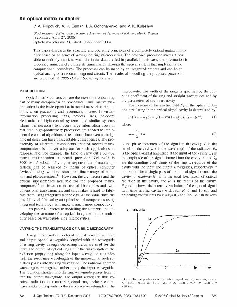
are the coupling coefficients of the ring waveguide of thecavity with the input and output waveguides, respectively, �is the time for a single pass of the optical signal around thecavity, a=exp�−��R�, � is the total loss factor of opticalradiation in the cavity, and R is the radius of the cavity.Figure 1 shows the intensity variation of the optical signalwith time in ring cavities with radii R=5 and 10 �m andbranching coefficients k=k1=k2=0.3 and 0.6. As can be seen
FIG. 1. Time dependences of the optical signal intensity in a ring cavity.1a—k=0.3, R=5; 1b—k=0.3, R=10; 2a—k=0.6, R=5; 2b—k=0.6, R=10 �m.
834120834-06$15.00 © 2006 Optical Society of America

from the figure, the optical-signal intensity in the cavityreaches saturation and the steady-state regime is establishedin the cavity in a definite time interval.
By changing the optical length of the cavity, it is pos-sible to displace its resonance wavelength and therebychange the signal intensity shunted into the cavity. If thecavity is fabricated from a semiconductor material, its opticallength can be changed, in particular, by changing the concen-tration of free charge carriers, and this alters the refractiveindex n of this material.
Carriers can be injected into a semiconductor material asa result of the so-called single-photon absorption effect.When a semiconductor material is optically pumped by pho-tons with an energy greater than its band gap, each absorbedphoton generates an electron–hole pair. The complex refrac-tive index of the semiconductor material upon injection offree carriers can be written as7,8
n = � − j , �3�where its real part � and imaginary part are determined by
�+,− = �±1
2�L −
�p2
�2 + �2�+1
2��L −
�p2
�2 + �2�2
+ � �p2
�2 + �2
�
��2�1/21/2
. �4�
The + and − signs relate, respectively, to the real part � andimaginary part of the complex refractive index. As can beseen from Eqs. �3� and �4�, the refractive index depends onthe permittivity L of the material, the plasma frequency �p,the carrier-collision frequency �=1/�, where � is the colli-sion time �the free path time� of the moving charge carriers,and the frequency � of the propagating optical radiation. Theplasma frequency is determined by
�p2 =
npe
0m* , �5�
where np is the free carrier density, e is the charge of a freeelectron, 0 is the permittivity of free space, and m* is theeffective mass of the carriers.
The transmittance T of the cavity �the intensity of thesignal at the output of the cavity� in the stationary state isdetermined by7,9
T =E2
2
E02 =
k12k2
2
1 − 2��1 − k12��1 − k2
2�a cos j� + �1 − k12��1 − k2
2�a2,
�6�where E2 is the signal amplitude at the cavity output. Thus,the transmittance is a function of the refractive index n of thecavity waveguide, which depends on the free-carrier concen-tration in accordance with Eqs. �3�–�5�. The dependences ofthe transmittance T of the cavity at the resonance wavelengthon the variations of the power Pcont of the optical controlsignal are shown in Fig. 2. It was assumed in the calculationsthat the optical waveguide of a ring microcavity is 0.7 �mwide and 0.5 �m thick and is made from gallium arsenide ona substrate of the same material with a buffer layer composedof AlGaAs.10 The buffer layer provides localization of theradiation in the waveguides. The carrier wavelength of thecontrolling optical analog signal �the pump signal� is
835 J. Opt. Technol. 73 �12�, December 2006
800 nm. The absorption coefficient of gallium arsenide atthis wavelength equals 104 cm−1. The parameters of galliumarsenide needed for calculating its refractive-index variationare taken from Ref. 11. As follows from Fig. 1, depending onthe cavity radius and the coupling coefficients, the time toestablish the steady-state regime can range from 3 to 40 ps.In accordance with this, the duration of the control signalwas taken to be equal to 20 and 40 ps when calculating thecurves in Fig. 2.
THE OPERATING PRINCIPLE AND OPTIMIZING THEPARAMETERS OF THE MATRIX MULTIPLIER
The structural layout of the matrix multiplier is shown inFig. 3. The main elements of the matrix multiplier are anoptically controllable array of waveguide ring microcavities3, an array of vertically radiating lasers 2, and linear arraysof LEDs 1 and photodetectors 4. The vertically radiatinglasers with controllable radiation intensity provide opticalpumping of each microcavity, which alters its transmission atthe signal wavelength.
As is well known, the operation by which one multipliesmatrix A= aij� of dimension m�r by matrix B= bij� of di-mension r�q is written in the form
C = A � B, �7a�
where C= cij� is the resultant matrix of dimension m�q,with
Ci1 = ai1 � b11 + ai2 � b21 + ai3 � b31 + ¯ + air � br1,
Ci2 = ai1 � b12 + ai2 � b22 + ai3 � b32 + ¯ + air � br2,
Ci3 = ai1 � b13 + ai2 � b23 + ai3 � b33 + ¯ + air � br3,
. . . . . . . . . . . . . . . . . . . . . . . . . . . . . . . . . . . . . . . . . . . . .
Ciq = ai1 � b1q + ai2 � b2q + ai3 � b3q + ¯ + air � brq,
�7b�
FIG. 2. Dependences of the optical signal intensity in a ring cavity withbranching coefficient k=k1=k2 on power Pcont and width �cont of the con-trolling optical signal. 1a—k=0.3, �=20; 1b—k=0.3, �=40; 2a—k=0.6, �=20; 2b—k=0.6, �=40 ps.
835Piliporich et al.

rray
where i=1,2 ,3 , . . . ,m.In the proposed optical multiplier, the components
a11,a12,a13, . . . ,a1r� of a row of matrix A are given by theoptical-signal intensities from the elements of the linear ar-ray of lasers 1 that arrive through the input waveguides at thecolumns of the optically controllable array of waveguide ringmicrocavities 3 �the first light-emitting element at the firstcolumn, the second at the second, etc.�, taking into accountthe coupling coefficients. In this case, the wavelengths�11,�12,�13, . . . ,�1r of the radiation arriving at each columnof the array of cavities are different. Components bij� of themultiplier matrix B are determined by the transmission coef-ficients of the elements of the array of microcavities, whichare specified by the optical-radiation intensities of the lasersof the array 2 of vertically radiating lasers. The lasers areadjusted so that the optical signals from each vertically radi-ating laser are projected onto the corresponding elements ofthe array of waveguide ring microcavities 3. In this case,
bij = Tij = Tij0 + ijPij
cont, �8�
where Tij are the transmittances of the elements of the arrayof waveguide microcavities, Tij
0 are the initial transmittancesof the microcavities in the absence of control signals, Pij
cont isthe radiation power of the lasers of the array of controllingvertically radiating lasers, and ij W−1� is a coefficient thatdetermines how the transmittance variation of the cavity de-pends on the supplied optical power �the tangent of the curvein Fig. 2�.
The microcavities of each column of the array of cavitiesare selected so that their resonance wavelengths correspondto the radiation wavelength �1j supplied to this column fromthe corresponding radiating element of the linear array 1 oflasers and differ from the resonance wavelengths of the cavi-ties of the other columns. Thus, the radiation wavelengths �1j
and � must differ by such an amount that the resonance
FIG. 3. Structural layout of the matrix multiplier based on waveguide ring3—optically controllable array of waveguide ring microcavities, 4—linear a
1,j+1
836 J. Opt. Technol. 73 �12�, December 2006
peaks of the corresponding cavities do not overlap. As fol-lows from Eqs. �3�–�6�, the controlling radiation of the cor-responding power from the elements of array 1 of verticallyradiating lasers alters the optical-signal intensities in the el-ements of the array of waveguide ring microcavities propor-tionally to the elements of the multiplicand matrix. Thus, theradiation intensity at the output of each microcavity is deter-mined by multiplying the intensity of the input radiation �theelements of a row of matrix A� and the transmission of themicrocavity, which depends on the intensity of the control-ling optical signal �the elements of matrix B�. From the out-put of the cavities, the radiation propagates along the outputwaveguides, which represent the rows of the array of wave-guide microcavities. Since the resonance wavelengths of thecavities in a row are different, so that their resonance peaksdo not overlap, the signals from the preceding cavities of theline are not shunted into the subsequent cavities but passdirectly to the linear array 4 of photodetectors. As a result,the radiation from all the elements of the corresponding rowof the optically controllable array 3 of waveguide ring mi-crocavities is incident on each photosensitive element of thelinear photodetector array, where it is summed in the charge-accumulation regime. The resulting energy obtained by thephotosensitive elements of the linear array 4 of photodiodesis the result of multiplying a row of matrix A by matrix B;i.e., it corresponds to the elements of rowc11,c12,c13, . . . ,c1q� of matrix C.
The elements of the subsequent rowsai1 ,ai2 ,ai3 , . . . ,air� of matrix A are given by the optical-signal intensities at other wavelengths. In this case, the ra-diation wavelengths of the elements of each kth column �ik
must differ from each other by the amount ��k=�i+1,k−�ik, amultiple of the resonance wavelength of the cavities of thiscolumn,
rocavities. 1—linear array of LEDs, 2—array of vertically emitting lasers,of photodetectors, 5—multiplexers, 6—demultiplexers.
mic
836Piliporich et al.

�res,k =Lkn
p, �9�
where Lk is the length of the cavities, which is identical forthe entire kth column, and p is a whole number. The radia-tion wavelengths �ij of all the rows of the multiplicand ma-trix A will thus correspond to resonance conditions.
As follows from the matrix-multiplication algorithmgiven in Eqs. �7�, matrix multiplier B acts identically on allthe rows of multiplicand matrix A. Therefore, all the rows ofthe matrix to be multiplied can be simultaneously enteredinto the array of controllable waveguide microcavities, whilethe multiplication of all the rows will also be carried outsimultaneously in one cycle. To form the optical signals ofthe elements of the different rows of the multiplicand matrix,a combined linear array of lasers representing a set of sepa-rate linear arrays is used, each of which forms the elementsof the corresponding row of the multiplicand matrix. Thesignals from the different lasers of an individual linear arrayare fed to each of the input waveguides through multiplexer5. The radiation of the elements of the different rows ofresultant matrix C is demultiplexed over the range of wave-lengths and is fed to an analogous combined linear array ofphotodetectors. Input multiplexers are no longer needed if alinear array of lasers with tunable wavelength is used. In thiscase, the tuning must be done in real time; for example, inthe lasers described in Ref. 13.
Thus, in the device considered here, a matrix composedof m�r elements is multiplied by a matrix with dimensionsr�q in one timing cycle. The summed optical signals ofelements cij� of the resultant matrix from the outputs ofdemultiplexers 6 can be directed not to photodetectors butalong waveguide lines to the next processing stages.
The energy and time characteristics of the matrix multi-plier can be optimized by varying the parameters of thewaveguide microcavities. As follows from Fig. 2, the powerof the controlling optical signal is small in cavities withsmall branching coefficients, but the switching time �the timeto establish the steady-state regime� of such cavities is rela-tively long. More rapid switching can be obtained by usingcavities with larger branching coefficients, but higher-powercontrol signals are needed in this case.
It is interesting that the power of the controlling opticalsignal is virtually independent of the cavity size. To switch acavity with a smaller radius, a larger carrier concentrationmust be created in it. The number of free carriers injectedinto the semiconductor material varies proportionally to thepower of the control signal. However, their concentration isinversely proportional to the size of the cavity. Consequently,when optical radiation of identical power is supplied, a largercarrier concentration is created in a microcavity of smallerradius.
In general, the dependence of the transmittance variationof a cavity on the supplied optical power coefficient ij inEq. �8�� is nonlinear. Therefore, to increase the accuracy withwhich an operation is carried out, the most linear section ofthe transfer characteristic of the ring cavity needs to be used;i.e., the information-signal intensity in the cavity must vary
837 J. Opt. Technol. 73 �12�, December 2006
within limits from 0.9 to about 0.2. The initial transmissionTij
0 of the microcavities corresponds to this minimum leveland is given by choosing the cavity parameters and the car-rier wavelength of the optical signal. As follows from Fig. 2,to obtain an intensity variation of the information signalwithin these limits, the range of power variations of the con-trol signal, depending on its duration and the coupling coef-ficients of the cavities, lies within the limits from 0–20 to0−150 mW.
Figure 4 shows the transfer characteristic of the matrixcomputer when the operation of matrix multiplication is car-ried out. The multiplication of matrices with dimensions m�2 and 2�2 is considered as an example. The row elementsa11 and a12 of multiplicand matrix A are given by input op-tical pulses P11
in and P12in , whose powers, respectively, equal
0.3 and 0.5 mW; the controlling optical pulses P11cont and
P12cont, P21
cont, and P22cont with powers, respectively, of 4, 8, 7,
and 6 mW, give elements b11, b12, b21, and b22 of multipliermatrix B, determined in accordance with Eq. �8�. The carrierwavelengths of pulses aij ��11=1.5544 �m and �12
=1.5558 �m� are chosen so that the initial transmission ofthe cavities in the absence of control signal Tij
0 equals about0.3. For microcavities with radii of 10 �m and branchingcoefficients k=0.3, the transmission coefficientsT11,T12,T21,T22, corresponding to the elements of multipliermatrix B, when control pulses Pij
cont are supplied, equal0.4875, 0.7542, 0.6815, and 0.6114. As a result, output opti-cal pulses P11
out and P12out, with powers of 0.224 and
0.280 mW, respectively, are supplied to the outputs of thelinear array of photodetectors, representing the row elementsc11 and c12 of resultant matrix C. In accordance with Eq. �9�,the elements of the second row of multiplicand matrix A canbe supplied at carrier wavelengths �21=1.5656 �m and �22
=1.5670 �m.The time to carry out the operation of multiplying matrix
A of optical signals by matrix B of the transmission of themicrocavities is made up of the time intervals for supplyingcontrol signals to an array of vertically emitting lasers, fortransmitting optical radiation over the longest input and out-put buses of an array of waveguide ring microcavities, whichis determined by the size of the elements being multiplied,and also the time to vary the transmission �the switchingtime� of the ring microcavities and the time for the photode-tectors to read out the signals. For a modern set of compo-nents, as used in integrated optics, the times to supply thecontrol signals to the array of vertically radiating lasers andto read out the signals by the photodetector can reach frac-tions of a nanosecond �0.01–0.1 ns�.4–6 The time to switchthe transmission of the microcavities, as follows from Fig. 1,does not exceed 20–40 ps. The lengths of the input and out-put waveguides of each microcavity are about 40 �m. Whena row of a matrix made up of 100 elements is multiplied, thetime for the optical signal to be transmitted over thewaveguides of the multiplier is about 0.01–0.02 ns. Thus,the time to carry out the operation of multiplying a matrix of
837Piliporich et al.

es th
dimension m�100 by a matrix of dimension 100�100 isless than 0.1 ns. In this case, the overall response rate ofmatrix multiplication is mainly limited by the throughput ofthe electric circuits to reload the digital input data aij and bij
and to digitize the output analog signals cij.
CONCLUSION
This paper has proposed a structure for a totally opticalmatrix multiplier based on an array of waveguide ring mi-crocavities that allow it to be fabricated in integrated form.The modelling that has been carried out has shown that suchan optical matrix processor possesses a response rate greaterthan 1010 vector multiplications per second and this, for amatrix dimension of 100�100 elements, gives a throughputgreater than 2m�1014 elementary operations per second,where m is the number of rows of the multiplicand matrixand is an optical analog of a modern integrated circuit. Theuse of a resonance system makes it possible to eliminate theinfluence of external destabilizing factors on the operation ofan optical matrix processor. The accuracy of the matrix mul-tiplication is determined by the linearity of the chosen sec-tion of the transfer characteristic of the ring microcavities, bythe stability of the carrier frequency in the linear array ofsemiconductor radiation sources, and by the process scatter
FIG. 4. Transfer characteristic of an array computer when it carries out therepresent the row elements a11 and a12 of multiplicand matrix A; P11
cont, P12cont,
b21, and b22 of multiplier matrix B; P11out and P12
out are the output optical puls
838 J. Opt. Technol. 73 �12�, December 2006
of the sizes of the ring microcavities in the array. When thesection of the transfer characteristic that is used is approxi-mated by a straight line ij =const in Eq. �8��, the multipli-cation error of a matrix made up of two columns reachesseveral percent, and this is acceptable for the operation ofanalog multiplication. If the number of elements of the mul-tiplicand matrix is increased, the calculations become moreaccurate because of statistical averaging of the deviations ofthe approximating straight line from the actual transfer char-acteristic. The optical matrix multiplier described here, withmicron dimensions of the elements from which it is made�radiators, microcavities, photodetectors�, makes it possibleto carry out matrix multiplication with parallel supply of theinitial data. In this case, information in a computer of such anarchitecture is processed during its transmission through theoptical system that implements the computational procedures�without using delay lines�. As a result, the information isprocessed in real time, actually in the time it takes radiationto propagate through the waveguides and cavities of the op-tical processor. The proposed matrix-multiplication methodmakes it possible to achieve the limiting possible productiv-ity, since all the operations are carried out optically and in asingle cycle.
ation of matrix multiplication. P11in and P12
in are the input optical pulses that, and P22
cont are the controlling optical pulses that represent elements b11, b12,at represent the row elements c11 and c12 of resultant matrix C.
operP21
cont
838Piliporich et al.

1Yu. A. Borisov, “The Trafik-monitor complex, based on the L18779VMprocessor,” Élektron. Nauka Tekhnol. Biz. No. 6, 58 �2003�.
2S. V. Sokolov, “Incoherent-optical matrix processor,” Opt. Zh. 65, No. 9,46 �1998� J. Opt. Technol. 65, 721 �1998��.
3A. A. Verbovetski�, “Modern methods of creating an optical digital com-puter technique,” Usp. Sovrem. Radioélektroniki No. 3, 12 �1999�.
4S. M. Zakharov, V. B. Fedorov, and V. V. Tsvetkov, “Optoelectronic inte-grated circuits utilising vertical-cavity surface-emitting semiconductor la-sers,” Kvant. Elektron. 28, No. 3, 189 �1999� Quantum Electron. 29, 745�1999��.
5N. A. Maleev, A. G. Kuz’menkov, A. E. Zhukov et al., “Design andfabrication technology for arrays for vertical-cavity surface-emitting la-sers,” Fiz. Tekh. Poluprov. 39, 487 �2005� Semiconductors 39, 462�2005��.
6A. Leven, V. Houtsma, R. Kopf et al., “InP-based double-heterostructurephototransistors with 135−GHz optical-gain cutoff frequency,” Electron.Lett. 40, 833 �2004�.
7
T. A. Ibrahim, W. Cao, and ’ Y. Kim, “Lightwave switching in semicon-839 J. Opt. Technol. 73 �12�, December 2006
ductor microring devices by free carrier injection,” J. Lightwave Technol.21, 2997 �2003�.
8C. H. Lee, P. S. Mak, and A. P. DeFonzo, “Optical control of millimeter-wave propagation in dielectric waveguides,” IEEE J. Quantum Electron.16, 277 �1980�.
9P. Rabiei, W. H. Steier, C. Zhang, and L. R. Dalton, “Polymer microringfilters and modulators,” J. Lightwave Technol. 20, 1968 �2002�.
10P. P. Absil, J. V. Hryniewiz, B. E. Little et al., “Vertically coupled micro-ring resonators using polymer wafer bonding,” IEEE Photonics Technol.Lett. 13, 49 �2001�.
11M. Shur, GaAs Devices and Circuits �Plenum Press, New York, 1987; Mir,Moscow, 1981�.
12G. A. Korn and T. M. Korn, Mathematical Handbook for Scientists andEngineers �McGraw-Hill, New York, 1961; Mir, Moscow, 1984�.
13V. A. Pilipovich, A. K. Esman, I. A. Goncharenko, and V. K. Kuleshov,“High-speed continuous tunable fibre and waveguide lasers with control-
lable Bragg grating,” Opt. Commun. 203, 289 �2002�.839Piliporich et al.