Embed Size (px)
Citation preview
1.Brief description
Name: APLACArea of application:APLAC is a universal program for ana-lysing and synthesising every conceiv-able circuit or system for telecommunica-tions, electronics and physics in a spe-cific time or frequency range. This in-cludes EM simulators, using the FDTDmethod.Most important positive characteristics:There is practically nothing that cannotbe investigated using APLAC.Just to show the application options, theparts list contains not only all the elec-tronics components previously known,but also models for mechanical oscilla-tion systems and shock absorbers. Andthe manual even provides an example ofthe simulation of RF energy absorptionin the human skull when a telephone callis made on a mobile phone.What I liked:All manuals are available for download-ing at no cost and constitute completetextbooks. All known microwave compo-nents and models of irregularities (fromthe microstrip bend through the interdig-
ital capacitor and length coupler throughto the circulator) are also released in thefree student version. An unbelievablycomprehensive library relating to func-tions and options, not just in electronics,but also in mathematics and physics.A good, easy to operate editor for “draw-ing” wiring diagrams.For experienced users and if all theeffects playing a role are included, thesimulation results tally precisely withreality.Problem areas:The program is a universal tool and isthus not equipped with easy to operatebutton control (like ANSOFT SER-ENADE). It operates in its own “APLAClanguage”, which initially requires theoperator to set up several “control ob-jects”. These are then combined to forma “simulation file” and executed. In plainlanguage this requires a lot of writingand separate programming for the solu-tion description, the sweep co-ordinatesand for displaying the results in dia-grams, text files or tables. In principle,this all represents a mixture of PSPICEand ARRL radio designer commandlines, together with elements of the pro-gramming language “C”.File type and file size:A download of approximately 45MB isrequired for all program sections and
Gunthard Kraus, DG8GB
An interesting programAPLAC
VHF COMMUNICATIONS 2/2003
90

manuals. Following installation, thatgives a Windows file of approximately65MB.No problems could be detected duringoperation using WIN 95/98/ME/ 2000/NT or fast computers.Bugs or serious miscalculations de-tected:Only insignificant little details or idi-osyncrasies (e.g. in the graphics structureor the print out), which could have beenclarified through the “APLAC Internethotline” using email. One pleasant thingis that any query to this hotline (whetherit is from a student or from an industrialfirm) is treated in an impartial andfriendly manner, and is handled compe-tently and free of charge.Desirable improvements:Intensive further development of whathas already been started, to make input-ting using wizards (small additional pro-grams with graphics user guides) consid-erably easier.Expansion of permissible simulation con-tent in free student version (see alsounder “Limitations”).User friendliness:As already pointed out, a very intensivefamiliarisation phase is required beforethe number of error messages followingthe start of a simulation is reduced.Perfect control is not achieved until sometime has elapsed and then only withcontinuous usage. Nevertheless, the op-erator has more to do than for similarproducts.Help:Very comprehensive online PDF manu-als in 7 volumes, each with approxi-mately 1,800 pages. Many examples ofcircuit and EM simulation as files on CD,together with discussion in the manual.Very friendly support, free of charge,obtainable via Internet or email.
Limitations:The free student version restricts thenumber of components to a maximum of12, although resistors, capacitors andcoils are not counted. In addition, themain memory in use during simulationmust not exceed a specific size, or elsethe processing is interrupted.One way out for experienced users insuch a case is to request the transfer to a45 day full test version free of charge.Acquisition options:Download student version from http://www.aplac.com or through “InternetTreasure Trove CDs” from VHF Com-munications.
2.A brief overall view
Professor Marti Valtonen developedAPLAC (Analysis Program for LinearActive Circuits) back in 1972 in its basicform. Since then, it has grown andflourished in the fertile soil of HelsinkiUniversity (and no doubt within thecountrys NOKIA culture as well). Asalready stated, the basic concept clearlygoes beyond the limits of the rival prod-ucts, which mainly specialise in certainspecific simulation areas and then lookfor business from customers with sophis-ticated operating systems.APLAC, on the other hand, is designedto handle every question, and bringstogether everything conceivable orknown in the world regarding simulationtools. This covers the PSPICE modulefor linear circuit simulation through theharmonic balanced simulator to non lin-ear large signal analyses, from the com-munications system simulator throughthe regulation of noise sidebands inoscillators right through to the EM simu-lation of microstrip antennas or RF ab-sorption in the human skull. It is only
VHF COMMUNICATIONS 2/2003
91

after an intensive study of the compre-hensive manuals that you discover every-thing you can do with this system.Universality like this naturally has to bepaid for, in this case with low userfriendliness. This means that you have toassemble everything yourself and youhave to tailor everything to the applica-tion in question. For this, you have to usethe systems own “APLAC language” thatyou may well take some time to get intoyour head and which you'll probablynever understand completely.Setting up the necessary simulation filesis similar to C programming. On the firstrun through there will be any number of
error messages, but with increasing expe-rience they can be eradicated ever morerapidly. Once this hurdle has been over-come, not only can we enjoy the preciseresults, but also the numerous investiga-tion and display options very quicklyconsole us for the relatively laboriousoperation.Now some simulations to explain theright way to use the software and simul-taneously demonstrate its efficiency.
2.1. First simulation example:S Parameter of a 110MHz Chebyshevlow pass filter
2.1.1.Setting up the circuit diagram
Before we can start up APLAC, thecomponent values of the desired low passfilter are determined, using one of thefree DOS filter programs from the Inter-net (e.g. “fds” or “faisyn20”). The fol-lowing attributes should apply here:
Fig 1: The results of a filter programfor a 110MHz Chebyshev low passfilter.
Fig 2: After starting APLAC press OK to start the editor.
VHF COMMUNICATIONS 2/2003
92

• Ripple = 0.1dB.
• Ripple limiting frequency, fg =110MHz
• Low inductance Implementation
• Degree of filtration, n = 5
• System resistance, Z = 50ΩThe result can be seen in Fig 1.Now we start up APLAC, the screen isshown in Fig 2. This shows how thecircuit diagram editor is started up. Usethe white drawing surface that appearsand make it full screen. We then rightclick the mouse somewhere in the freearea of the screen. A new menu appearsand we select “Basic”. This calls up thelist of basic components, and we canselect an inductance, using the term“Ind” (Fig 3). Following confirmation,using the <ENTER> key, the coil issuspended from the cursor and is depos-ited in the wiring diagram. Repeat thesequence and you will have the two colis
required. Any component used is alsolisted under “BASIC / RECENT” andcan be called up from there.Now we call up the three capacitorsunder the term “Cap”. However, eachtime they are placed they must be rotatedthrough 90° using the key combination<CONTROL> + <R>. We also needthree earth symbols, in the basic parts listthe earth symbol is shown as "Ground".Finally we double click on the graphicfor each component and enter its value inthe “Attributes” field. Do not forget tomake the numbering of the componentand its attributes visible using “ShowName” and “Show all Attributes”. Whena value is entered always use decimalpoints (American notation) and not com-mas!And now for the wiring, just double leftclick anywhere in the free area of thewiring diagram, and a “wire coil” willsuddenly be suspended from the cursor.Click on the connection of a componentand the wire then uncoils to the nextconnection desired.The connections here may, and should,run in curving, oblique lines over thecircuit. Just left click again, and theeditor itself will automatically turn thewiring into very neat right angled shapes!For input and output, right click to callup a port via “Basic” and deposit thesymbol on the input side. Then repeat onthe other side for the output port. If youconnect the two ports to the circuit and toearth, then you should have a wiringdiagram corresponding to Fig 4. (Pleasealways make all attributes visible afterdouble clicking on a symbol). Lookingcarefully you will notice that the systemimpedance is pre-set to 50Ω for bothports.To see the details better you should zoomin on the circuit to make it full screen. Todo this, go into the “View” menu andselect “Zoom Whole Diagram”. Youhave now finished drawing the circuit.
Fig 3: This menu opens after a rightmouse click on a free part of thescreen. Then the required part can bechosen.
VHF COMMUNICATIONS 2/2003
93

In addition to this, the simulated data forthe low pass filter can also be writteninto an S parameter file in Touchstoneformat (with the ending “*.s2p”). To dothis, click on the output port symbol andenter the corresponding requirementSTORE “LPF110MHz.s2p” GHZ MAfor the attributes (in a new line followingthe 50Ω system impedance).
2.1.2. Circuit simulation
First, open the “Object List Box” (Fig 5)and double click on it. In the menu whichopens, first select the setting “Isweep”and then remove it with “Delete”, be-cause this is an “interactive Windowssweep”, that should not be used here.Replace this by a new sweep type objectand type the following settings:
Explanation:1st line:The term “110MHz_low_pass” is auto-matically used as the name of the projectfor each diagram and results print outand is included on the print out
2nd line:Carry out a simulation in the frequencyrange and divide the range from 100kHzto 3GHz linearly into 1001 simulationsteps.3rd line:Enter “Window=0” for the results printout set up for a plot diagram with thevertical axis numbered from -50 to 0dB.Note:The blank line separates the simulationsection from the print out section andshould therefore never be forgotten!5th line:Show the curves for S11 and S22 in dBin the window number zero.Now re-open the “Presentation” menu.The sweep file has to be made visible onthe screen. To do this, click on “ShowControl Object”, select “Sweep” from thelist and close with “OK”.Two little things should be mentionedbefore starting the simulation. First, youmust save the current project under asuitable name in a suitable directory.Secondly, make a final visual check ofthe object box list, as the sweep file mustalways be right at the bottom of the list(otherwise you will receive an errormessage which is difficult to under-stand). Fig 6 shows what everythingshould look like.If all settings are correct, start the simula-tor, using the key combination <Control+ S>. The results can be zoomed to full
Fig 4: Thecompleted circuitdiagram inAPLAC.
"110MHz_low_pass"LOOP 1001 FREQ LIN 100KHZ 0.3GHZWINDOW=0 Y "" "dB" -50 0
...SHOW W=0 DB S(1,1)+ DB S(2,1)
VHF COMMUNICATIONS 2/2003
94

screen in the usual Windows maner asshown in Fig 7.To see the Chebyshev ripples in S21should move the cursor to the lowestvalue in the vertical scale, the cursor thenhas a small additional directional arrow.As an example, click on the value “-50dB”, a short menu opens and type “-0.4dB”. Enter “OK” and you will see Fig 8,thus demonstrating that the filter pro-grams calculations are correct.
Anyone wanting more details shouldinvestigate the two menus “Scales” and“Options”, there are several options foraltering the results diagram.
2.2. Second simulation example:low noise MMIC amplifier
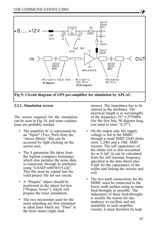
The full circuit diagram for a GPS
Fig 5: Openingthe Object ListBox to set up therequired sweepobject.
Fig 6: Thecompletedsettings forsimulation of the110MHz low passfilter.
VHF COMMUNICATIONS 2/2003
95

pre-ampl i f ie r (mean f requency:1,575.42MHz) can be seen in Fig 9. Thenoise matching required has already beencarried out by two microstrips at theinput. The printed circuit board materialis to be double sided Rogers 0.813mmthick (25 MIL). The underside forms acontinuous earth surface, with the earthconnections on the topside being con-nected by a sufficient number of feed-throughs.
Thus a brief APLAC task list for thissimulation might be:The behaviour of the circuit in the fre-quency range from 0.1 to 10GHz shouldbe described through the S parametersand the curve for the noise factor, F (indB). You should also check whether anystability problems can be expected withthe circuit.
Fig 7: APLACsimulation resultsfor the 110MHzlow pass filtershowing S11 andS22.
Fig 8:Repositioning thedisplay clearlyshows theChebyshevripples in the S21curve.
VHF COMMUNICATIONS 2/2003
96
2.2.1. Simulation screen
The screen required for the simulationcan be seen in Fig 10, and some explana-tions are probably needed.
• The amplifier IC is represented byan “Nport” (Two_Port) from the“macro library” that can beaccessed by right clicking on thescreen area.
• The S parameter file taken fromthe Agilent companys homepage,which also includes the noise data,is connected, through its attributesusing “LOAD=m86563v5.s2p”.This file must be copied into thevalid project file for our circuit.
• A “Prepare” object should bepositioned in the object list box(“Prepare Noise”), which willprepare the noise simulation.
• The two microstrips used for thenoise matching are first simulatedas ideal lines which are “Tline” inthe basic menu (right click
mouse). The impedance has to beentered in the attributes. Theelectrical length is in wavelengthsof the frequency, FC=1,575MHz(for the first line, 90 degrees long,you need to enter “0.25”).
• On the output side, the supplyvoltage is fed to the MMICthrough a small SMD 22nH choke(size: 1,206) and a 10Ω SMDresistor. The self capacitance ofthe choke coil is also accountedfor as 0.1pF (it can be calculatedfrom the self resonant frequencyspecified in the data sheet) also0.2pF for the capacitance of thesolder pad linking the resistor andcoil.
• The two earth connections for theMMIC must be connected to thelower earth surface using as manyfeed-throughs as possible. Theinductance of these feed-throughsis usually the reason for anytendency to oscillate and anyinstability in such amplifiercircuits, it must therefore be kept
Fig 9: Circuit diagram of GPS pre-amplifier for simulation by APLAC.
VHF COMMUNICATIONS 2/2003
97

as low as possible! If we set avalue of approximately 1nH perfeed-through per 1mm of printedcircuit board, it then follows thatwith 10 feed-throughs on eachside, we can expect a totalinductance of about 0.05nH. Thisinductance is shown as componentL3 in the circuit, so that it can beused to monitor the stability.
• A 50Ω port is connected to theinput and another to the output asterminations.
2.2.2. Sweep file to simulate S param-eter and noise factor
This file (as always, as the last positionin the Object Box List) must look like:
Explanation:In the first half (before the blank line) wehave first the circuit name “MGA86563-Amplifier” (it will be shown in everyresult following the simulation). This isfollowed by the requirement to simulatea maximum of 1001 points in the fre-quency range from 100MHz to 10GHz(maximum value for free student ver-sion).In the following three diagrams (Window= 0 to Window = 2) a grid is pro-grammed for the vertical axis instead ofdB divisions, in order to make the valueseasier to read off. The display range inthe first diagram (for S11 and S22!) goesfrom 40 to 0dB, whereas a range from 0to + 40dB makes more sense in Window1 for S21. A scale from 0 to 4dB is thebest choice for the noise factor. Now(never forget this!) a blank line is re-quired.The subsequent display notes for thediagrams are probably self explanatory.Window 2 is programmed to display boththe noise factor actually obtained and thetheoretical minimum possible (NFopt).Finally, press <Control + S> on thekeyboard to start the simulation.
Fig 10: The simulation screen of the GPS pre-amplifier for APLAC. See textfor explanation of components.
"MGA86563-Amplifier"LOOP 1001 FREQ LIN 0.1GHZ 10GHZWINDOW=0 Y "" "dB" -40 0 GRIDWINDOW=1 Y "" "dB" 0 40 GRIDWINDOW=0 Y "" "dB" 0 4 GRID
SHOW W=0 Y MagdB(S(1,1))+ Y MagdB(S(2,2))+ W=1 Y MagdB(S(2,1))+ W=2 Y NoiseFigure+ Y MinNoiseFigure Marker=1
VHF COMMUNICATIONS 2/2003
98

2.2.3. First simulation results
Following some calculation time, theresults appear on the screen. Click toselect the desired window into the fore-ground and zoom. The values for theinput reflection, S11, and the outputreflection, S22, are shown in Fig 11. Thecurve for S22, in particular, gives nocause for complaint, and only gets betteras the frequency becomes higher. S11, onthe other hand, is determined by thenoise matching circuit and must be ac-cepted as it is. Under “Options”, you willfind the option “Probe”, using this youcan go to each point of a curve and theassociated value will be shown in the topleft hand corner of the screen.In the S21 curve, shown in Fig 12, theonly cause for complaint might be thatthe maximum amplification is at a higherfrequency than ideal. We get a very niceresult from Fig 13, where the noisefactor, between 1GHz and 2.5GHz, isvery close to the minimum value
2.2.4. Stability control
2.2.4.1. Basic requirements forstability
The best circuit will be of no use if it hasa tendency to uncontrollable self excita-tion, i.e. if it oscillates after assembly. Inthe specialist literature and in practice,various checks are standard, which allmake use of the S parameters of thecircuit using specific guidelines.The oldest and best known method willnow be examined in greater detail. Itoperates using the stability factors “K”and “B1”These two variables are dependent onlyon the S parameters of the two portnetwork used and not on the termina-tions. They can be used to express thecondition for “absolute freedom fromoscillation under all conditions and loadand/or internal resistances” (uncondi-tional stability) in the following manner:K > 1 and B1 > zero
The two variables are calculated from the
Fig 11:Simulation resultsfor the GPSpre-amplifiershowing S11 andS22 up to 10GHz.
VHF COMMUNICATIONS 2/2003
99

S parameters in the following manner(but we naturally leave this to a pro-gram....):
and
where:
Note:APLAC no longer uses this technique,but instead makes a total of three moremodern but very different control func-tions available:
Fig 12:Simulation resultsfor the GPSpre-amplifiershowing S21 upto 10GHz.
Fig 13:Simulation resultsfor the GPSpre-amplifiershowing noisefigure.
2112222111 222
SSSS
K⋅
∆+−−=
222 221111 ∆−−+= SSB
21122211 SSSS ⋅−⋅=∆
VHF COMMUNICATIONS 2/2003
100

First option:Following the method just discussed (andperhaps also because many people arestill so used to it), the following variantscan be used by calling up the “S_K” and“S_D” functions:The stability factor K must exceed 1AND the S matrix determinant D = ∆must be less than 1, if the circuit is to bestable overall (unconditionally stable).Second option:We can work with only a single stabilityfactor “µ” and exercise control using thefunction “S_u”. Then we have:
The stability factor µ must exceed 1 ifthe circuit is to be “unconditionally sta-ble” overall.Third option:This most modern solution would be theone to fulfil the “Nyquist criterion”. It isdescribed as an “Advanced stabilityanalysis” (see APLAC Users Guide, Vol-ume 2, pp. 3-26) and represents the“standardised determinants function” inthe complex plane, using the option“NDF”. It maintains that:As soon as the origin (“zero point”) ofthis complex plane is not embraced bythe NDF curve, the circuit remains stableoverall.But for this an analysis must first becarried out in the time domain e.g. usingan AC source because results cannot beobtained by just using the S parameters.So this option has been omitted.
2.2.4.2. Stability control using K and∆∆∆∆ and also using µµµµ
Methods 1 and 2 are combined for theamplifier project. Naturally, a fewchanges are needed in the sweep file forthis purpose:
• In the simulation section, we needa third window for the threestability control factors. Thegraduation of the scale should gofrom 0 to 4.
• In the display section, we arrangethat "D", "K" and "µ” are not onlydisplayed but are also markeddifferently.
This sweep file can be seen In Table 1(the additions are marked in bold):(Note: In this section of the sweep file,the change from the instruction “SHOW”to “DISPLAY” is deliberate. “DIS-PLAY” is the complete function for alltypes of representations that require morecalculations to be carried out but alsooffer more options. “SHOW” is therapid, slimmed down version with re-stricted capabilities, it is not adequate forthe stability factors.The result of this simulation is shown inFig 14. In spite of the total feed-throughinductance of 0.05nH transferred into thecircuit as a precaution, the circuit re-mains stable over the entire frequencyrange (K and µ exceed 1overall, whereasD is less than 1 or 0.5).
2.2.4.3. Additional control using thestability circuits
The minute you get involved with cir-cuits that have a tendency to oscillateonly at specific internal resistances orloads (potentially unstable devices), themethod described in the previous section,using the three factors K, µ and D, is nolonger adequate. We know only that atendency to oscillate can arise as soon asK or µ falls below 1 or D exceeds 1, butwe do not know the critical conditionsyet. More comprehensive analyses areneeded here, which give a result in theform of two circles showing preciselythese unstable areas of the associatedreflection factors in the Smith diagram.One circle shows how the stability, K,
VHF COMMUNICATIONS 2/2003
101

depends on the load (more correctly, onthe associated reflection factor, LOAD),the associated technical expression is:Stability K (Load Plane)The other circle shows how the stability,K, depends on the internal resistance ofthe source (better: once again, on theassociated reflection factor, SOURCE).
Here the technical expression is:Stability K (Source Plane)Yet both these “stability circles” are onlyvalid for a single frequency and thesimulation must be repeated if the fre-quency is changed.Thus the circuit can often still be stablefor a specific frequency if the internalresistance or load is known and constant,although the stability factors, K, µ and Dare already warning of a potentiallyunstable situation.A very simple rule applies for the evalua-tion of the circles:
• If both circles (for SOURCE orLOAD) run completely outsidethe Smith diagram, the circuit isguaranteed to be unconditionallystable.
• It is likewise unconditionallystable if the Smith diagram (forSOURCE or LOAD) iscompletely surrounded (i.e.enclosed) by a stability circle. Thatsounds a little crazy, but thebackground is as follows. Thecentre of the stability circle thenlies in the infinite and its circular
"MGA86563-Amplifier"LOOP 1001 FREQ LIN 0.1GHZ 10GHZWINDOW=0 Y "" "dB" -40 0 GRIDWINDOW=1 Y "" "dB" 0 40 GRIDWINDOW=0 Y "" "dB" 0 4 GRIDWINDOW=3 Y "" "" 0 4 GRID
SHOW W=0 Y MagdB(S(1,1))+ Y MagdB(S(2,2))+ W=1 Y MagdB(S(2,1))+ W=2 Y NoiseFigure+ Y MinNoiseFigure Marker=1DISPLAY WINDOW 3 Y "D" S_D+ Y "K" S_K Marker=1+ Y "µµµµ" S_u Marker=2
Table 1: Modified sweep file.
Fig 14:Simulation resultsfor the GPSpre-amplifiershowing stability.
VHF COMMUNICATIONS 2/2003
102

area covers the entire universe, butstill leaves the Smith diagram free.To help you visualise this, you canimagine a globe. Push a pin intoGermany, which represents thecentre of the Smith chart. Stickanother pin into the other side ofthe globe e.g. in California, whichrepresents the centre of thestability circle.If we now continually increase theradius of the “Californian stabilitycircle”, then it will finallyapproach the pin in Germany fromall sides around the globe.Eventually it is pinned into a tinylittle free area and that is thestable region expected, in whichthere is still no oscillation.
In both cases, “conventional analysis”simultaneously gives a value of K > 1, µ>1 and D<1.But if any parts of the circles are insidethe Smith diagram, then the circuit oscil-lates if the internal resistance or load liesin the intersection zones. Then K is also< 1 or µ < 1 or D > 1!It is thus the developers task to checkwhether, in practical operation, these
critical resistances can occur. If not, thenthe circuit can be implemented by carefuldesign and can function reliably.APLAC is able to do the calculation offunctions corresponding to these circleswhich we must call up. They are:S_CS for the centre and S_RS for theradius of the source stability circle, to-gether with S_CL for the centre andS_RL for the radius of the load stabilitycircle.And now here's an interesting thing,which is probably not something any ofAPLACs competitors can offer:Using “manual programming” of theAPLAC sweep file, you can easily (e.g.by entering the following):LOOP 1 FREQ LIN 1.57542GHz1.57542GHzhave the ratios and all selected param-eters displayed for a single individualfrequency (here 1.57542GHz). But onlyAPLAC will also calculate and show allthe associated stability circles for a widerfrequency range during sweeping!All other products (e.g. APPCAD, An-soft, etc.) are restricted here to a singleselectable design frequency.
Fig 15:Simulation resultsfor the GPSpre-amplifiershowing thesmith diagramfor the sourceside.
VHF COMMUNICATIONS 2/2003
103

As a final step in the amplifier project,this can be viewed. To do this, expandthe sweep file again adding two Smithdiagrams with the radius R=3:The result of the work can be seen in Fig15 for the source side, and in Fig 16 forthe load side. It has already been estab-lished that the circuit is stable, but nowwe can see the safety margins for thedifferent frequencies and can, if neces-sary, pick individual frequencies out,using “Probe”, for more precise analyses.Nor would it be a problem to look atunstable regions and work out whichsource impedances or load impedances toavoid and then permit “restricted opera-tion”, e.g. with precise 50Ω loads.That can become important for mostPHEMTs that have been designed for useat 10GHz and almost always have atendency to oscillate at low frequencies.We can use just such tricks for suchprojects as a super low noise Meteosat or2 meter pre-amplifier with a noise figureof less than 0.5dB to permit clean opera-tion.
2.3. Simulation using real microstrips
In conclusion, Fig. 17 shows the ampli-fier circuit, where the ideal transmissionlines have been replaced at the input bytwo actual microstrips with differentwidths and (to correct the effects whenlines with different widths meet together)a “symmetrical Mstep”. Microstrips canbe called up using: “right click mouse /Microwave / Microstrip / Mlin(stripline).The circuit dimensions required werecalculated using several programs forcomparison. First using PUFF, then us-ing the stripline calculator TRL85, thenusing the microstrip calculator from thenew AppCAD, version 3.0, and finallyusing a self written APLAC microstripcalculator (APLAC merely prepares thenecessary functions for this users have tocompile the calculation instructionsthemselves). There were no significantdifferences. Likewise, the new amplifiersimulations fully coincide with the valuesfrom the previous section.
Fig 16:Simulation resultsfor the GPSpre-amplifiershowing thesmith diagramfor the load side.
VHF COMMUNICATIONS 2/2003
104

3.Summary
APLAC offers an almost incrediblenumber of options, but presents itselfwith a very plain and simple user inter-face. That means that, in comparisonwith other products, considerably moretraining is needed and routine use isdecidedly harder work. Yet if we con-sider that all the simulations and investi-gations presented were undertaken exclu-sively using the free student version,things look much better. The authortherefore uses this student version for thesimulation of all those things which arenot available in the familiar PUFF sys-tem, and often exchanges simulation re-sults or partial solutions between the twoprograms in the form of S parameterfiles.Even using the free version, there is nobarrier to such things as impedancejumps or open ended extensions ofmicrostrips, interdigital capacitors,bends, etc. Yet the message “Memoryrestricted in this version” often puts a
damper on ones enthusiasm in such ap-plications.However, the author considers himselffortunate finally to have convinced hisdepartment to procure a full versionunder the APLAC university programme.As a consequence of this, a 120 pageAPLAC tutorial has been created in foursections:
• Part 1: Training + simulations intime domain and frequency rang
• Part 2: Investigation of digitalcircuits
• Part 3: Passive microwave andmicrostrip circuits
• Part 4: Active microwave circuitsPart 1 has also been translated intoEnglish for an international introductorycourse in our school.A copy of this “APLAC-CD” can beobtained from the author by email at costprice: [email protected]
Fig 17: Circuit diagram for the GPS pre-amplifier with microstrip lines forinput matching.
VHF COMMUNICATIONS 2/2003
105