Embed Size (px)
Citation preview
AN INTEGRATED ULTRASOUND TRANSDUCER
DRIVER FOR HIFU APPLICATIONS
by
Wai Wong
A Thesis
Presented to Lakehead University
in Partial Fulfillment of the Requirement for the Degree of
Master of Science
in
Electrical and Computer Engineering
Thunder Bay, Ontario, Canada
September 19, 2013

Abstract
Wai Wong, An Integrated Ultrasound Transducer Driver for HIFU Applications (Under the Su-
pervision of Dr. Christoffersen, Dr. Curiel and Dr. Pichardo).
This thesis proposes an MRI-compatible integrated CMOS amplifier that is capable of di-
rectly driving an ultrasound transducer for HIFU applications. The output stage of the integrated
amplifier operates in class DE mode with its output directly connected to a shunt capacitor and
an ultrasound transducer without the need for an inductor. This design was simulated with
Spectre R© simulator using the 0.8 µm 5/20 V CMOS process data available from Teledyne-
DALSA Semiconductor. The proposed integrated amplifier has an efficiency of 80% with 1 W
of output power at 1 MHz and achieves an acceptable level of third harmonic. A layout of the
integrated amplifier was prepared. The integrated amplifier occupies a die area of approximately
2.5 mm by 1.6 mm including input-output pads.

Biographical Summary
Wai Wong completed a BEng in Electrical Engineering in 2011 and is currently pursuing a
master’s degree in Electrical Engineering both from Lakehead University, Thunder Bay, Ontario.
He has also served as a Graduate Assistant at his institution for two years. His research interests
include analog circuit design and communications. He is a student member of the Institute of
Electrical and Electronics Engineers (IEEE).
Part of this thesis has been published as the conference paper, “An Integrated ultrasound
Transducer Driver for HIFU applications” which was presented at the 26th Annual Canadian
Conference on Electrical and Computer Engineering, CCECE 2013, Regina, SK, hosted by the
IEEE Canada in May 2013.
i

Acknowledgments
This thesis would not have been possible without the support of Lakehead University, the
Thunder Bay Regional Research Institute, the Natural Sciences and Engineering Research Coun-
cil, and CMC Microsystems.
It gives me great pleasure in acknowledge Dr. Carlos Christoffersen, my supervisor, for pro-
viding support for this thesis, as well as his expertise in circuit design and the Cadence Design
System, and his ideas and advice. I wish to thank Dr. Laura Curiel and Dr. Samuel Pichardo
for sharing their in-depth knowledge of ultrasound transducers and High Intensity Focused Ul-
trasound.
I would also like to thank to Mr. Aaron Pearson for proofreading this thesis.
Finally, I thank my family for their encouragement, patience, and understanding.
Wai Wong
ii

Contents
List of Figures v
List of Tables ix
List of Symbols x
List of Abbreviations x
1 Introduction 2
1.1 Motivations and Objectives of this Study . . . . . . . . . . . . . . . . . . . . . . . 2
2 Literature Review 4
2.1 Introduction . . . . . . . . . . . . . . . . . . . . . . . . . . . . . . . . . . . . . . . 4
2.2 Review of Amplifier Topologies . . . . . . . . . . . . . . . . . . . . . . . . . . . . 4
2.2.1 Analog Amplifiers . . . . . . . . . . . . . . . . . . . . . . . . . . . . . . . . 4
2.2.2 Switched Amplifiers . . . . . . . . . . . . . . . . . . . . . . . . . . . . . . . 7
2.2.3 Other topologies for Switched Amplifier . . . . . . . . . . . . . . . . . . . 13
2.3 Review of Published Designs . . . . . . . . . . . . . . . . . . . . . . . . . . . . . . 15
2.4 Summary . . . . . . . . . . . . . . . . . . . . . . . . . . . . . . . . . . . . . . . . 24
3 Characterisation of an Ultrasound Transducer 27
3.1 Transducer . . . . . . . . . . . . . . . . . . . . . . . . . . . . . . . . . . . . . . . . 27
3.2 Equivalent Circuit . . . . . . . . . . . . . . . . . . . . . . . . . . . . . . . . . . . 28
3.3 Mathematical Model . . . . . . . . . . . . . . . . . . . . . . . . . . . . . . . . . . 29
3.4 Results . . . . . . . . . . . . . . . . . . . . . . . . . . . . . . . . . . . . . . . . . . 32
iii
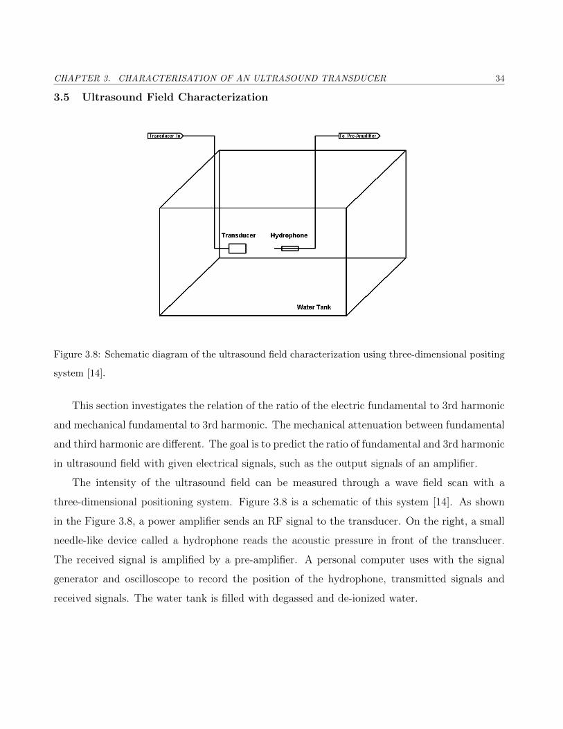
3.5 Ultrasound Field Characterization . . . . . . . . . . . . . . . . . . . . . . . . . . . 34
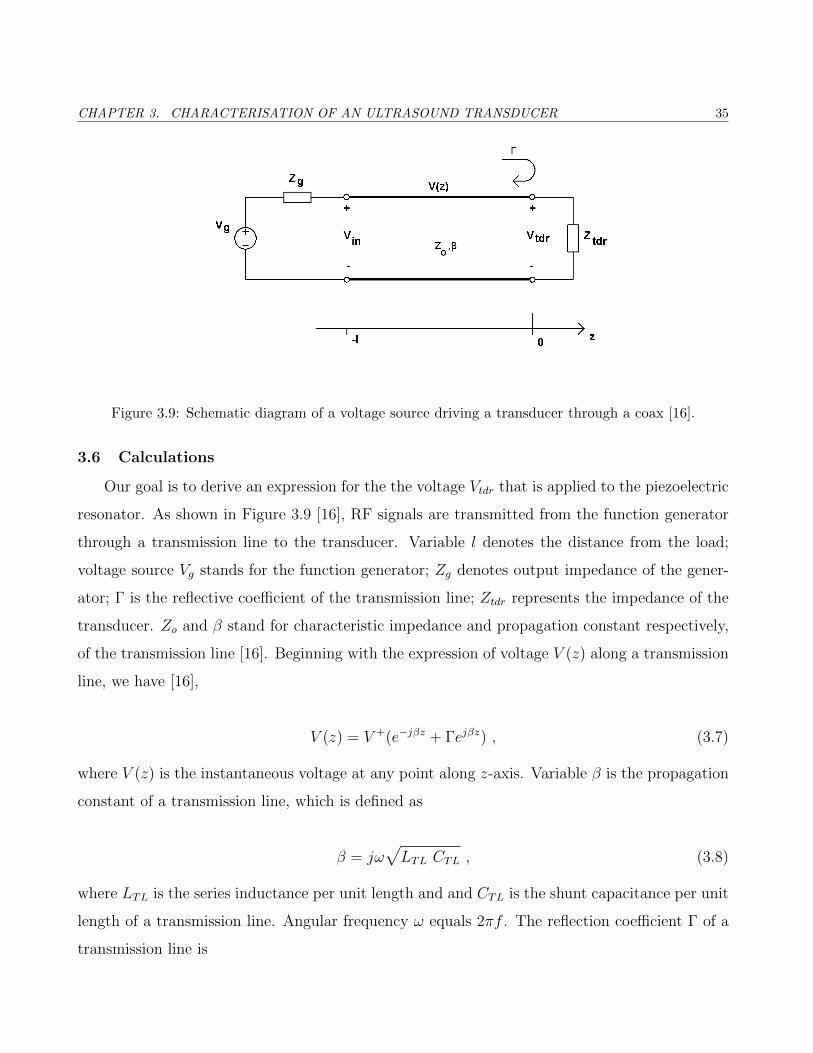
3.6 Calculations . . . . . . . . . . . . . . . . . . . . . . . . . . . . . . . . . . . . . . . 35
3.7 Results . . . . . . . . . . . . . . . . . . . . . . . . . . . . . . . . . . . . . . . . . . 37
4 Amplifier Design 38
4.1 Introduction . . . . . . . . . . . . . . . . . . . . . . . . . . . . . . . . . . . . . . . 38
4.1.1 CMOS process kit . . . . . . . . . . . . . . . . . . . . . . . . . . . . . . . 39
4.2 Class DE Amplifier . . . . . . . . . . . . . . . . . . . . . . . . . . . . . . . . . . . 39
4.2.1 Tuning of a practical class DE amplifier . . . . . . . . . . . . . . . . . . . 48
4.2.2 Calculations . . . . . . . . . . . . . . . . . . . . . . . . . . . . . . . . . . . 50
4.3 Gate Driver . . . . . . . . . . . . . . . . . . . . . . . . . . . . . . . . . . . . . . . 56
4.3.1 Calculations . . . . . . . . . . . . . . . . . . . . . . . . . . . . . . . . . . . 58
4.4 Current Mirror . . . . . . . . . . . . . . . . . . . . . . . . . . . . . . . . . . . . . 60
4.5 Digital Block . . . . . . . . . . . . . . . . . . . . . . . . . . . . . . . . . . . . . . 63
5 Simulation Results 66
5.1 Pre-layout simulations . . . . . . . . . . . . . . . . . . . . . . . . . . . . . . . . . 66
5.2 Post-layout simulations . . . . . . . . . . . . . . . . . . . . . . . . . . . . . . . . . 70
6 Conclusions 74
6.1 Future Work . . . . . . . . . . . . . . . . . . . . . . . . . . . . . . . . . . . . . . . 75
A Transducer Housing 76
B Results of the Attenuation of Harmonics with 20 Vp−p Sinusoidal Signals 78
C An Estimation of M4’s width using the Differential Equation Method 79
D Schematic Diagram 82
E Layout View 92
References 106
iv
List of Figures
2.1 Biasing points of classes A, B, and AB amplifiers [4]. . . . . . . . . . . . . . . . . 5
2.2 Block diagram of a single transistor RF amplifier [5]. . . . . . . . . . . . . . . . . 6
2.3 Output waveforms of classes A, B and AB amplifiers [5]. . . . . . . . . . . . . . . 6
2.4 Class D half-bridge voltage switching amplifier [5]. . . . . . . . . . . . . . . . . . . 8
2.5 Class D full-bridge voltage switching amplifier [5]. . . . . . . . . . . . . . . . . . . 9
2.6 Voltage and current waveforms of class D full-bridge voltage switching amplifier [5]. 9
2.7 Topology of class E amplifier [5]. . . . . . . . . . . . . . . . . . . . . . . . . . . . 11
2.8 Voltage and current waveforms of class E amplifier [5]. . . . . . . . . . . . . . . . 12
2.9 Topology of class DE amplifier with one shunt capacitor [5]. . . . . . . . . . . . . 12
2.10 Topology of Step-up driving [6]. . . . . . . . . . . . . . . . . . . . . . . . . . . . . 13
2.11 Topology of flyback driving [6]. . . . . . . . . . . . . . . . . . . . . . . . . . . . . 14
2.12 Topology of Push-pull driving [6]. . . . . . . . . . . . . . . . . . . . . . . . . . . . 15
2.13 Schematic of DC to RF Inverter [7]. . . . . . . . . . . . . . . . . . . . . . . . . . . 16
2.14 Schematic of class D inverter for piezoelectric transducer [8]. . . . . . . . . . . . . 16
2.15 Magnitude impedance of piezoelectric ultrasound transducer[8]. . . . . . . . . . . 17
2.16 Schematic of switching amplifier and tuned filter [2]. . . . . . . . . . . . . . . . . . 18
2.17 Schematic of class D amplifier for Audio Beam System [9]. . . . . . . . . . . . . . 19
2.18 Schematic of power inverter for harmonic cancellation [10]. . . . . . . . . . . . . . 20
2.19 Waveform of harmonic cancellation [10]. . . . . . . . . . . . . . . . . . . . . . . . 20
2.20 Schematic of class E amplifier with PFC [11]. . . . . . . . . . . . . . . . . . . . . 22
2.21 Schematic of switched-mode amplifier [12]. . . . . . . . . . . . . . . . . . . . . . . 22
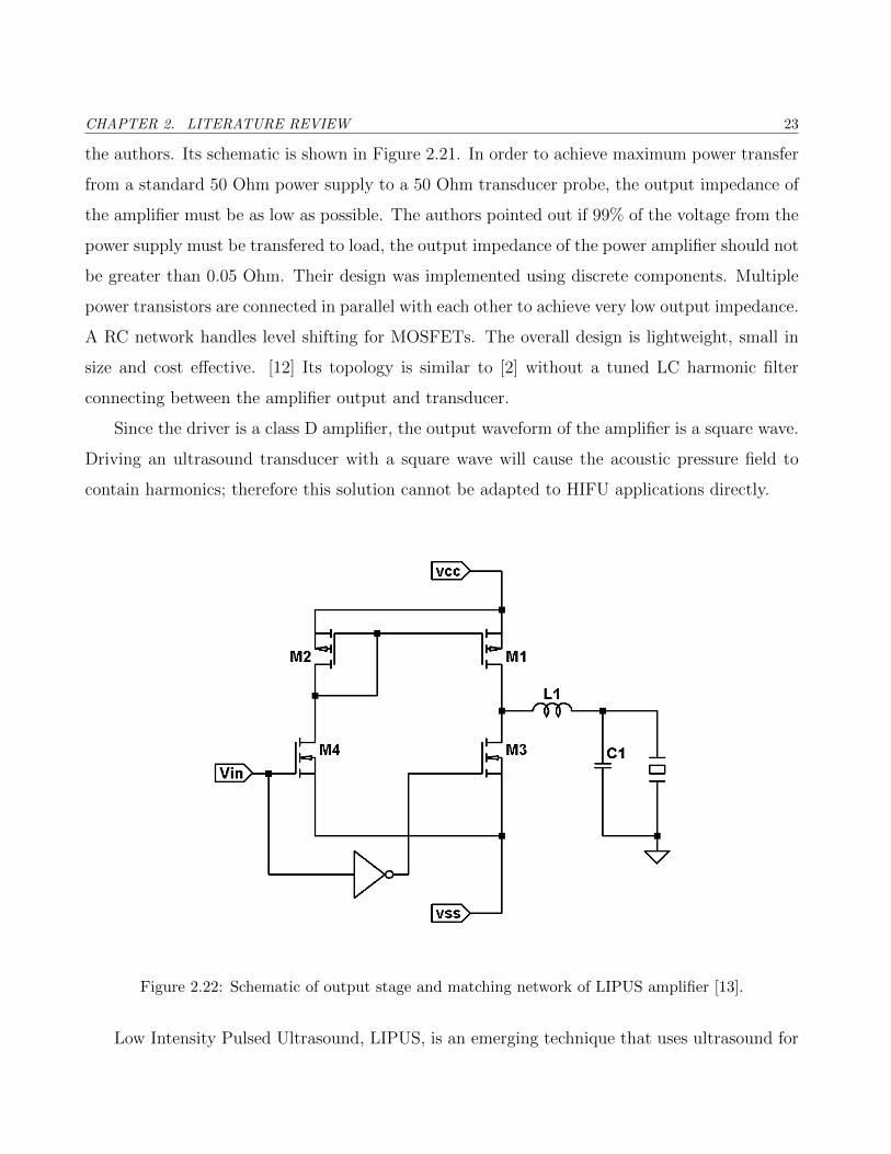
2.22 Schematic of output stage and matching network of LIPUS amplifier [13]. . . . . . 23
v
3.1 Exploded view of a transducer. . . . . . . . . . . . . . . . . . . . . . . . . . . . . 27
3.2 Equivalent circuit of a piezoelectric resonator near its resonance frequency [15]. . . 28
3.3 Impedance of equivalent circuit in Figure 3.2 [15]. . . . . . . . . . . . . . . . . . . 29
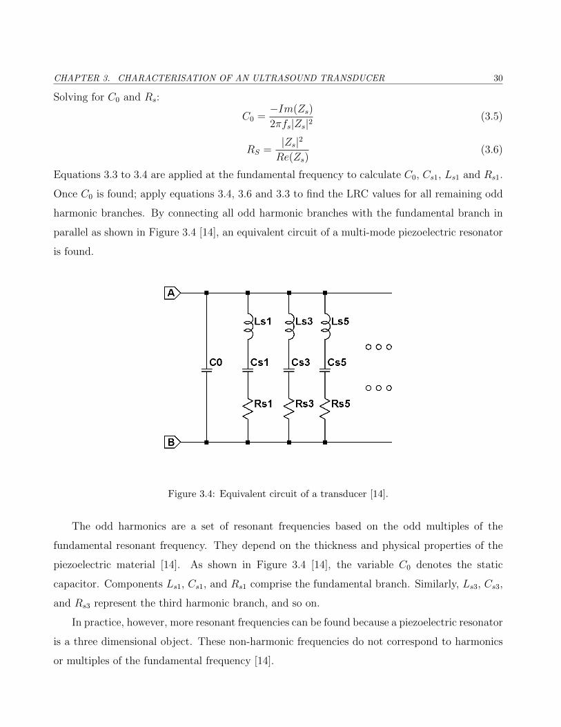
3.4 Equivalent circuit of a transducer [14]. . . . . . . . . . . . . . . . . . . . . . . . . 30
3.5 Comparison of the impedance of ultrasound transducer and equivalent circuit on
a Smith Chart from 300 kHz to 300 MHz. . . . . . . . . . . . . . . . . . . . . . . 31
3.6 Equivalent circuit of the piezoelectric resonator up to the 9th harmonic. . . . . . . 32
3.7 Comparison of the impedance of equivalent circuit and the measured results from
VNA between 300 kHz and 6 MHz. . . . . . . . . . . . . . . . . . . . . . . . . . . 33
3.8 Schematic diagram of the ultrasound field characterization using three-dimensional
positing system [14]. . . . . . . . . . . . . . . . . . . . . . . . . . . . . . . . . . . 34
3.9 Schematic diagram of a voltage source driving a transducer through a coax [16]. . 35
4.1 Block diagram of the integrated amplifier for ultrasound transducer. . . . . . . . . 38
4.2 Symbol of high-voltage and low-voltage MOSFET used in this report. . . . . . . . 40
4.3 Topology of class DE amplifier with one shunt capacitor [5]. . . . . . . . . . . . . 40
4.4 Voltage waveforms of class DE amplifier [5]. . . . . . . . . . . . . . . . . . . . . . 41
4.5 Current waveforms of class DE amplifier [5]. . . . . . . . . . . . . . . . . . . . . . 42
4.6 Equivalent circuits of class DE amplifier at different stages [5]. . . . . . . . . . . . 44
4.7 Tuning procedure for class DE amplifier recommended by Albulet [19]. . . . . . . 49
4.8 Schematic of technological parameters extraction. . . . . . . . . . . . . . . . . . . 52
4.9 Square root of MOSFET drain current√ID as a function of gate-to-source voltage
VGS. . . . . . . . . . . . . . . . . . . . . . . . . . . . . . . . . . . . . . . . . . . . 53
4.10 Simulation results of√ID as a function of VGS. . . . . . . . . . . . . . . . . . . . 54
4.11 Schematic diagram of the gate driver for each power MOSFET [21]. . . . . . . . . 57
4.12 Schematic diagram of current mirror and current source [21]. . . . . . . . . . . . 60
4.13 Schematic diagram of the digital block. . . . . . . . . . . . . . . . . . . . . . . . . 64
4.14 Map for input functions and output of the digital block. . . . . . . . . . . . . . . 65
5.1 Amplifier output voltage waveforms versus time at steady state. . . . . . . . . . . 67
5.2 Drain current waveforms of M701 and M702 against time at steady state. . . . . . 67
vi

5.3 Discrete Fourier Transform of the amplifier’s output voltage waveforms at steady
state. . . . . . . . . . . . . . . . . . . . . . . . . . . . . . . . . . . . . . . . . . . . 68
5.4 Percentage of third harmonic to fundamental of the amplifier output waveform as
a function of switch-on duty ratio D with varying external capacitance at steady
state. . . . . . . . . . . . . . . . . . . . . . . . . . . . . . . . . . . . . . . . . . . . 69
5.5 Efficiency versus switch-on duty ratio D with a varying external capacitance at
steady state. . . . . . . . . . . . . . . . . . . . . . . . . . . . . . . . . . . . . . . . 69
5.6 Output power against switch-on duty ratio with a varying external capacitance at
steady state. . . . . . . . . . . . . . . . . . . . . . . . . . . . . . . . . . . . . . . . 70
5.7 Layout of the integrated amplifier. . . . . . . . . . . . . . . . . . . . . . . . . . . . 72
5.8 Output voltage waveforms of pre- and post-layout simulations. . . . . . . . . . . . 73
5.9 Output current waveforms of pre- and post-layout simulations. . . . . . . . . . . . 73
6.1 Projected percentage of third harmonic to fundamental in the acoustic pressure
waveform as a function of switch-on duty ratio D with varying external capacitance. 75
A.1 Transducer Housing . . . . . . . . . . . . . . . . . . . . . . . . . . . . . . . . . . . 77
D.1 Schematic diagram for simulating the integrated amplifier. . . . . . . . . . . . . . 83
D.2 Top level schematic of the integrated amplifier. . . . . . . . . . . . . . . . . . . . . 84
D.3 Block diagram of the integrated amplifier. . . . . . . . . . . . . . . . . . . . . . . 85
D.4 Block diagram of M701 gate driver. . . . . . . . . . . . . . . . . . . . . . . . . . . 86
D.5 Schematic diagram of M701 gate driver. . . . . . . . . . . . . . . . . . . . . . . . 87
D.6 Block diagram of M702 gate driver. . . . . . . . . . . . . . . . . . . . . . . . . . . 88
D.7 Schematic diagram of M702 gate driver. . . . . . . . . . . . . . . . . . . . . . . . 89
D.8 Schematic diagram of the digital block. . . . . . . . . . . . . . . . . . . . . . . . . 90
D.9 Schematic diagram of the ultrasound transducer. . . . . . . . . . . . . . . . . . . . 91
E.1 Final integrated amplifier layout. . . . . . . . . . . . . . . . . . . . . . . . . . . . 93
E.2 Layout with M701 Gate driver. . . . . . . . . . . . . . . . . . . . . . . . . . . . . 94
E.3 Layout with M702 Gate driver. . . . . . . . . . . . . . . . . . . . . . . . . . . . . 95
E.4 Layout with M217 / M317. . . . . . . . . . . . . . . . . . . . . . . . . . . . . . . . 96
vii
E.5 Power transistors M701 and M702 layout. . . . . . . . . . . . . . . . . . . . . . . 97
E.6 Layout with transistor M203. . . . . . . . . . . . . . . . . . . . . . . . . . . . . . 98
E.7 Layout with transistor M204 . . . . . . . . . . . . . . . . . . . . . . . . . . . . . . 99
E.8 Layout with transistor M303. . . . . . . . . . . . . . . . . . . . . . . . . . . . . . 100
E.9 Layout with transistor M304. . . . . . . . . . . . . . . . . . . . . . . . . . . . . . 101
E.10 Layout with transistors M209 / M309 and M210 / 310. . . . . . . . . . . . . . . . 102
E.11 Layout with M211 - M214 / M311 - M314. . . . . . . . . . . . . . . . . . . . . . . 103
E.12 Layout with current mirror, M215 / M315 and M216 / M316. . . . . . . . . . . . 104
E.13 Layout with combinational circuit block. . . . . . . . . . . . . . . . . . . . . . . . 105
viii

List of Tables
2.1 Comparison of amplifier topologies. . . . . . . . . . . . . . . . . . . . . . . . . . . 25
2.2 Comparison of specifications of published works. . . . . . . . . . . . . . . . . . . . 26
3.1 Attenuation of harmonics with 2 Vp−p sinusoidal signals. . . . . . . . . . . . . . . 37
4.1 Conditions of ZVS and ZDS. . . . . . . . . . . . . . . . . . . . . . . . . . . . . . . 46
4.2 The expressions of class DE amplifier output voltage and current waveforms. . . . 47
4.3 A summary of the extracted technological parameters. . . . . . . . . . . . . . . . 55
4.4 Estimated size, gate capacitance, drain capacitance and channel resistance of tran-
sistors used in an earlier design. . . . . . . . . . . . . . . . . . . . . . . . . . . . . 55
4.5 Transistor dimensions in the final design. . . . . . . . . . . . . . . . . . . . . . . . 62
4.6 Truth Table. . . . . . . . . . . . . . . . . . . . . . . . . . . . . . . . . . . . . . . . 64
B.1 Attenuation of harmonics with 20 Vp−p sinusoidal signals. . . . . . . . . . . . . . . 78
ix
List of Symbols
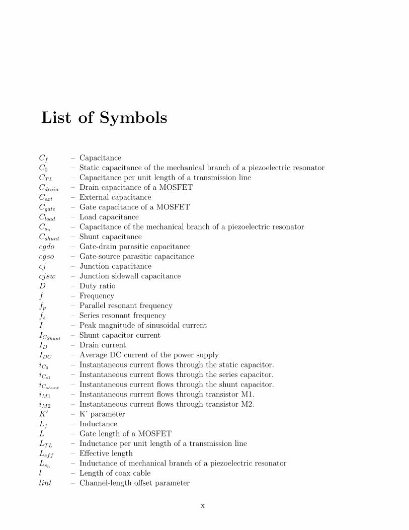
Cf – CapacitanceC0 – Static capacitance of the mechanical branch of a piezoelectric resonatorCTL – Capacitance per unit length of a transmission lineCdrain – Drain capacitance of a MOSFETCext – External capacitanceCgate – Gate capacitance of a MOSFETCload – Load capacitanceCsn – Capacitance of the mechanical branch of a piezoelectric resonatorCshunt – Shunt capacitancecgdo – Gate-drain parasitic capacitancecgso – Gate-source parasitic capacitancecj – Junction capacitancecjsw – Junction sidewall capacitanceD – Duty ratiof – Frequencyfp – Parallel resonant frequencyfs – Series resonant frequencyI – Peak magnitude of sinusoidal currentICShunt – Shunt capacitor currentID – Drain currentIDC – Average DC current of the power supplyiC0 – Instantaneous current flows through the static capacitor.iCs1 – Instantaneous current flows through the series capacitor.iCshunt – Instantaneous current flows through the shunt capacitor.iM1 – Instantaneous current flows through transistor M1.iM2 – Instantaneous current flows through transistor M2.K ′ – K’ parameterLf – InductanceL – Gate length of a MOSFETLTL – Inductance per unit length of a transmission lineLeff – Effective lengthLsn – Inductance of mechanical branch of a piezoelectric resonatorl – Length of coax cablelint – Channel-length offset parameter
x

M(f) – The sensitivity of the hydrophone corresponding to a particular frequencyP – PowerPatt – Attenuation in dBQ – Quality factorRsn – Resistance of mechanical branch of a piezoelectric resonatorRch – Channel ResistanceT – Duration of a cycle or periodTON – Duration of Switch-onTp – Propagation delayTintrinsic – Primitive delay of a logic gateTdrive – A dynamic factor for propagation delay depends on the load.t – timetfall – Fall timetrise – Rise timetox – Gate oxide thicknessV cc – Supply voltageV pp – High voltage supplyVDS – Drain-to-source voltageVGS – Gate-to-source voltageVadj – Received signals were adjusted by hydrophone sensitivity.Vg – Function generator voltageVh – Amplified output signal from the hydrophoneVin – Voltage appears at the input of the coax.Vm – Peak magnitude of voltage across output resistorVp−p – Peak-to-peak voltageV ov – Overdrive voltageVt – Threshold voltagevDS – Instantaneous drain-to-source voltageW – The gate width of a MOSFETZ – ImpedanceZL – Load impedanceZin – Impedance seen from the coaxial cable at fsZo – Characteristic impedance of a transmission lineZs – Impedance at fsZtdr – Impedance reflected from the piezoelectric resonator. fs
Γ – Reflective coefficientβ – Propagation constantε0 – Permittivity of free airεr – Relative permittivityψ – Phase angleθ – Factor of mobility degradation
xi

2θ – Angle of conductionω – Angular frequency
List of Abbreviations
HIFU – High Intensity Focused UltrasoundHV – High-VoltageIC – Integrated CircuitLC – Inductor and CapacitorPZT – Lead Zincorate TitaniateLPF – Low Pass FilterLV – Low-VoltageMOSFET – Metal Oxide Semiconductor Field Effect TransistorNMOS – N-type metal oxide semiconductorPMOS – P-type metal oxide semiconductorPWM – Pulse Width ModulationRC – Resistor and capacitorRF – Radio FrequencyRFC – Radio Frequency ChokeTTL – Transistor to Transistor LogicVNA – Vector Network AnalyzerZVS – Zero Voltage SwitchingZDS – Zero Derivative Switching
Chapter 1
Introduction
1.1 Motivations and Objectives of this Study
HIFU, or High Intensity Focused Ultrasound, is a non-invasive surgical technique that ther-
mally ablates tissue in human organs, such as the liver, without the need of incision. Tumor
ablation is achieved by focusing acoustic energy that translates into heat energy delivered to the
focal zone of the ultrasound transducer [1]. As it is a very precise operation, any movements,
such as respiration, of the patient’s body may displace the focal zone and healthy tissue may
be damaged. HIFU operation can be guided by Magnetic Resonance Imaging (MRI) so that
tissue temperature can be monitored and any body movements can be compensated for in real
time. Such development entails a multi-element HIFU transducer array that offers electronic
focusing and sufficient pressure distribution, because it is necessary to produce a proper focal
pattern without damaging the surrounding tissue [2]. Each element of an array is piloted by
different phase information so as to create sufficient level of acoustic pressure at the focal zones.
A sophisticated multi-element ultrasound transducer array may have over a thousand elements,
which results in a very complex connections setup if the amplifier can not be kept close to the
transducers. Therefore, downscaling the ultrasound therapy equipment becomes an interesting
subject of study. The objective of this thesis is to design a CMOS power amplifier for a piezo-
electric transducer to be installed near the piezoelectric resonator. Several of the challenges of
designing the integrated amplifier are outlined below:
1. Each amplifier should occupy minimum possible area.

CHAPTER 1. INTRODUCTION 3
2. The use of magnetic components, such as inductors, should be eliminated because they can
interfere with the MRI’s reception and distort the image [3].
3. To preclude overheating, the amplifier must be highly efficient.
4. It is capable of delivering 1 W of power to the load with an acceptable level of harmonics.
Thesis Overview
Chapter 2 scrutinizes the applicability of analog amplifiers and switched amplifiers as well as
typical published works on the subject of our project. Chapter 3 discusses the characterization
of the ultrasound transducer and introduces a lump element model for the ultrasound trans-
ducer used in circuit simulation. Chapter 4 covers details of the circuit design, analysis of the
class DE amplifier, methods of CMOS parameter extraction, and the design of transistors and
gate drivers. Chapter 5 summarizes the simulation results, including output power, efficiency,
ratio of third harmonic to fundamental, and a comparison of the pre-layout and post-layout
simulations. Appendices D and E contain schematic diagrams and layout views of the proposed
integrated amplifier that was used in Spectre R© and Virtuoso R© for simulations.
Chapter 2
Literature Review
2.1 Introduction
The original objective of this study was to review any antecedent published works on MRI-
compatible HIFU integrated amplifiers. Unfortunately, published works on this topic were never
found; furthermore, published works on integrated amplifier for ultrasound therapy are extremely
scarce. As a result, this chapter reviews published works on piezoelectric amplifiers and scruti-
nizes their applicability to our problem. This chapter is organized as follows: Section 2.2 reviews
some basic topologies of analog amplifiers and switched amplifiers. Section 2.3 covers several
published works that relate to the design of piezoelectric amplifiers. Section 2.4 summarizes the
studies and concludes the chapter.
2.2 Review of Amplifier Topologies
2.2.1 Analog Amplifiers
Analog amplifiers, such as classes A, B, and AB, are distinguished by their biasing conditions
and angles of conduction. Output transistors are controlled by gate-to-source voltage, VGS so
that they are operating as dependent-current sources in saturation mode during amplification.
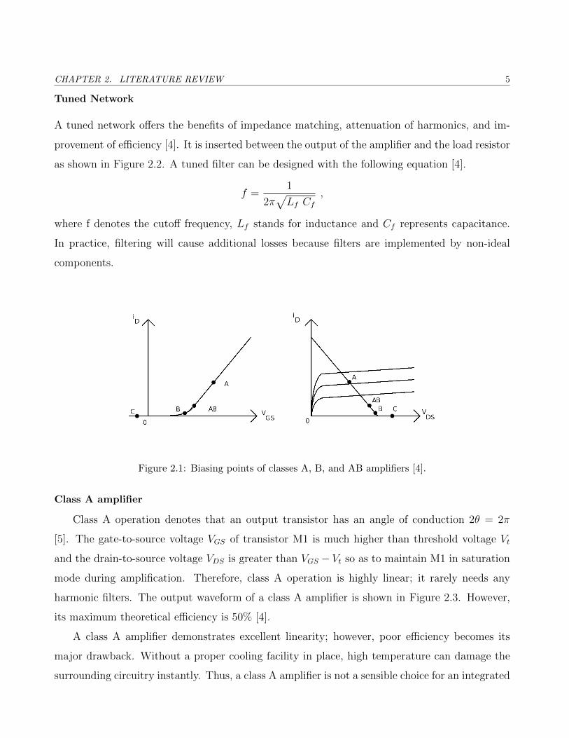
Figure 2.1 shows the biasing conditions of class A, B, and AB amplifiers [4]. A general schematic
is illustrated in Figure 2.2 [4].
CHAPTER 2. LITERATURE REVIEW 5
Tuned Network
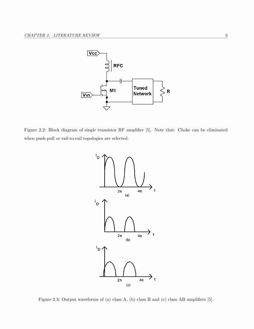
A tuned network offers the benefits of impedance matching, attenuation of harmonics, and im-
provement of efficiency [4]. It is inserted between the output of the amplifier and the load resistor
as shown in Figure 2.2. A tuned filter can be designed with the following equation [4].
f =1
2π√Lf Cf
,
where f denotes the cutoff frequency, Lf stands for inductance and Cf represents capacitance.
In practice, filtering will cause additional losses because filters are implemented by non-ideal
components.
Figure 2.1: Biasing points of classes A, B, and AB amplifiers [4].
Class A amplifier
Class A operation denotes that an output transistor has an angle of conduction 2θ = 2π
[5]. The gate-to-source voltage VGS of transistor M1 is much higher than threshold voltage Vt
and the drain-to-source voltage VDS is greater than VGS − Vt so as to maintain M1 in saturation
mode during amplification. Therefore, class A operation is highly linear; it rarely needs any
harmonic filters. The output waveform of a class A amplifier is shown in Figure 2.3. However,
its maximum theoretical efficiency is 50% [4].
A class A amplifier demonstrates excellent linearity; however, poor efficiency becomes its
major drawback. Without a proper cooling facility in place, high temperature can damage the
surrounding circuitry instantly. Thus, a class A amplifier is not a sensible choice for an integrated
CHAPTER 2. LITERATURE REVIEW 6
Figure 2.2: Block diagram of single transistor RF amplifier [5]. Note that: Choke can be eliminated
when push-pull or rail-to-rail topologies are selected.
Figure 2.3: Output waveforms of (a) class A, (b) class B and (c) class AB amplifiers [5].

CHAPTER 2. LITERATURE REVIEW 7
amplifier if sufficient cooling is unavailable.
Class B amplifier
Class B operation stands for an output transistor that has an angle of conduction 2θ = π
[5]. The biasing voltage VGS of the power transistor is equal to Vt. In this case, transistor M1
enters active region when VGS > Vt and VDS > VGS − Vt . Therefore, only half of a period is
being reproduced by the amplifier; this is shown in Figure 2.3. The quiescent bias current of a
class B amplifier is equal to the threshold current.
The crucial challenges of class B amplifier include low efficiency and output distortion. The
theoretical maximum efficiency of a class B amplifier is 78.5% [4]. Moreover, since only the
positive half of a sinusoidal waveform is being reproduced, complementary topology, such as
pull-push, must be used. However, crossover distortion occurs when both transistors are not
conducting.
Class AB amplifier
A class AB operation denotes an output transistor that has an angle of conduction π ≤
2θ ≤ 2π [5]. Voltage VGS is greater than or equal to Vt, and VDS > VGS − Vt. The theoretical
maximum efficiency of a class AB amplifier is between 50% and 78.5%, depending on the design.
The output waveforms of class AB amplifier are shown in Figure 2.3.
Although a class AB amplifier offers a balance of efficiency and harmonics, similar to the
class B amplifier, its theoretical maximum efficiency is too low for our needs.
2.2.2 Switched Amplifiers
For the remainder of this section, we will review several switched amplifiers that are poten-
tially suitable for HIFU integrated amplifier design. Switched amplifiers are another group of
power amplifiers that is commonly used in many applications due to their simple circuity and
high efficiency. Unlike any analog amplifier, a switched amplifier operates its output transistors
as switches. It is either transfers all voltage to the load when the switch is turned on or no
voltage to the load when the switch is off. For that reason, the theoretical maximum efficiency
is 100%. In practice, the efficiency of a switched amplifier is limited by switching loss, non-zero
CHAPTER 2. LITERATURE REVIEW 8
channel resistance and harmonics [4].
Class D amplifier
Figure 2.4: Class D half bridge voltage switching amplifier (a) Square wave, (b) PWM [5].
The schematic of the class D amplifier is shown in Figure 2.4 (a) [5]. Switches M1 and M2 will
be turned on alternately at 50% duty cycle, to charge and discharge a tuned network. The drain
terminals of M1 and M2 are connected to a tuned network that is responsible for attenuating the
harmonics because the output waveforms from the amplifier are square waves. The theoretical
maximum efficiency of a class D amplifier is 100%; however, in practice, the efficiency is reduced
by parasitic loss of the switches and filtering loss [4]. Furthermore, the design of the gate driver
CHAPTER 2. LITERATURE REVIEW 9
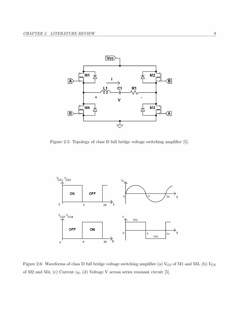
Figure 2.5: Topology of class D full bridge voltage switching amplifier [5].
Figure 2.6: Waveforms of class D full bridge voltage switching amplifier (a) VGS of M1 and M3, (b) VGS
of M2 and M4, (c) Current iR, (d) Voltage V across series resonant circuit [5].
CHAPTER 2. LITERATURE REVIEW 10
for the class D amplifier is usually complicated and costly because of the high voltage present at
the terminal of M1 [6]. Moreover, interference generated by the power supply may be present at
the driving circuit output [6].
Pulse width modulation (PWM) is another way of operating a class D amplifier. This idea
is illustrated in Figure 2.4 (b). PWM is a modulation technique that converts the input signals
to a series of square pulses with their duty ratios directly proportional to the electrical level of
the input signals. The switching frequency of PWM should be at least 10 times higher than the
frequency of input [4] [8]. The output low pass filter (LPF) serves multiple tasks including signal
recovery, impedance matching, and noise reduction [8].
The class D full-bridge amplifier comprises four transistors and a tuned network. Its topology
and waveforms are illustrated in Figure 2.5 and Figure 2.6 [5]. From 0 to π radians, switches
M1 and M3 conduct; M2 and M4 are opened. The voltage V across the series resonant circuit
is +V cc. Between π and 2π radians, switches M2 and M4 conduct; M1 and M3 are opened.
The voltage V becomes −V cc. Thus, the magnitude of output voltage is doubled because the
direction of the current is manipulated by switches. The power delivered to the load R1 is
quadrupled [5]. A class D full-bridge can also be driven by PWM.
In general, a class D amplifier should be operated beyond the resonant frequency of the tuned
network. This is because current spikes created by the leading current of a capacitive load with
respect to the voltage can cause a breakdown of a parasitic bipolar transistor inside a MOSFET
during an on-off transition [5]. To alleviate the situation, several measures can be taken, such as
using snubber circuits, connecting an inductor in series with MOSFETs, choosing high-voltage,
or high on-resistance transistors [5].
The class D half-bridge amplifier is a very popular choice of output stage for ultrasound
therapy applications [2] [12] [13]. For class D half and full bridge amplifiers, the output voltages
are square waves which are unsuitable for transducers. A tuned filter must be used to attenuate
harmonics because the output waveforms are square waves. The maximum efficiency drops
to 81% if there is no filtering in place [4]; this can be verified by dividing the power of the
fundamental to the power of the square wave. Although full bridge configuration offers higher
output power, it also doubles the output parasitic capacitance and the occupied area.
Using PWM with a class D amplifier for driving piezoelectric transducers requires a low pass

CHAPTER 2. LITERATURE REVIEW 11
filter to remove high frequency components. Therefore, this technique has the best chance of
recovering the original signals. However, the harmonics of the PWM’s switching frequency can
interfere with the MRI’s reception. In practice, parasitic loss of MOSFETs increases with the
increase of switching frequency [13].
Figure 2.7: Topology of class E amplifier [5].
Class E amplifier
A class E amplifier is a single switch amplifier with a theoretical efficiency of 100%. Figure 2.7
and Figure 2.8 illustrate its topology and waveforms. Unlike with the other amplifiers mentioned
above, the tuned network is part of the class E amplifier. Tuned network allows vDS to slowly
decline to zero exactly at the moment when M1 conducts. Since voltage vDS across the switch is
zero, the switching loss is also zero. It is called zero-voltage-switching ZVS [5]. In addition, the
derivative of vDS is also zero at the point where ZVS takes place; this is called zero-derivative-
switching [5], ZDS. Reference [11] is an example of using a class E amplifier to drive a piezoelectric
transducer.
The major drawback of a class E amplifier is the need for an RF choke that is used to limit
the current ripples generated by switching. For 10% current ripples, the minimum inductance of
the choke is approximately 8.7 times the series resistance Rs, divided by the switching frequency
[5]. So, it is not a suitable solution for an integrated amplifier, because the available room for
the die is very limited.
CHAPTER 2. LITERATURE REVIEW 12
Figure 2.8: Waveforms of Class E amplifier. (a) On-off signals, (b) Current waveforms through resistor,
(c) Drain-to-source voltage waveforms [5].
Figure 2.9: Topology of class DE amplifier with one shunt capacitor [5].
CHAPTER 2. LITERATURE REVIEW 13
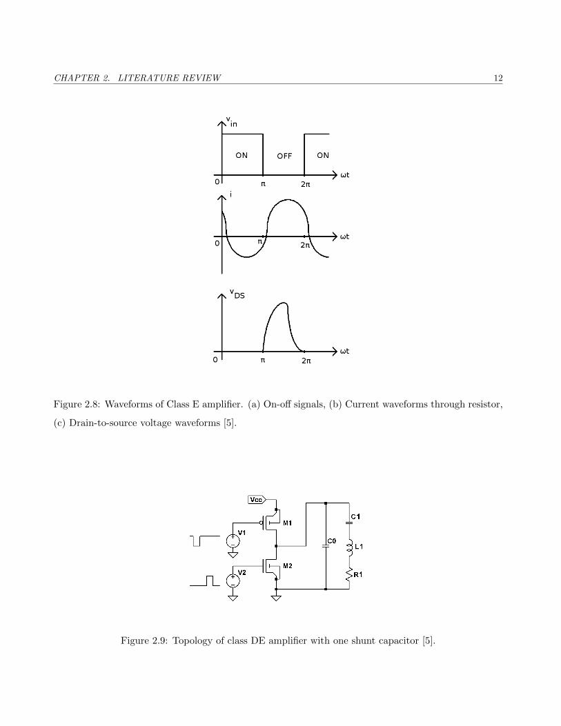
Class DE amplifier
A class DE amplifier integrates class D amplifier topology and class E switching condition.
It has a theoretical efficiency of 100%. Figure 2.9 illustrates the basic topology of a class DE
amplifier. Switches M1 and M2 turn on and off alternately with a duty ratio of 0.25; therefore,
two time gaps of 0.25 T are created between pulses to allow ZVS and ZDS to take place. A
detailed analysis of the class DE amplifier is provided in Chapter 4.
Much as other switching amplifiers, the output waveform of a class DE amplifier contains a
moderate level of harmonics; additional filtering will be required for HIFU applications. Since it
is a switched amplifier, parasitic loss appears when ZVS and ZDS do not perform precisely.
2.2.3 Other topologies for Switched Amplifier
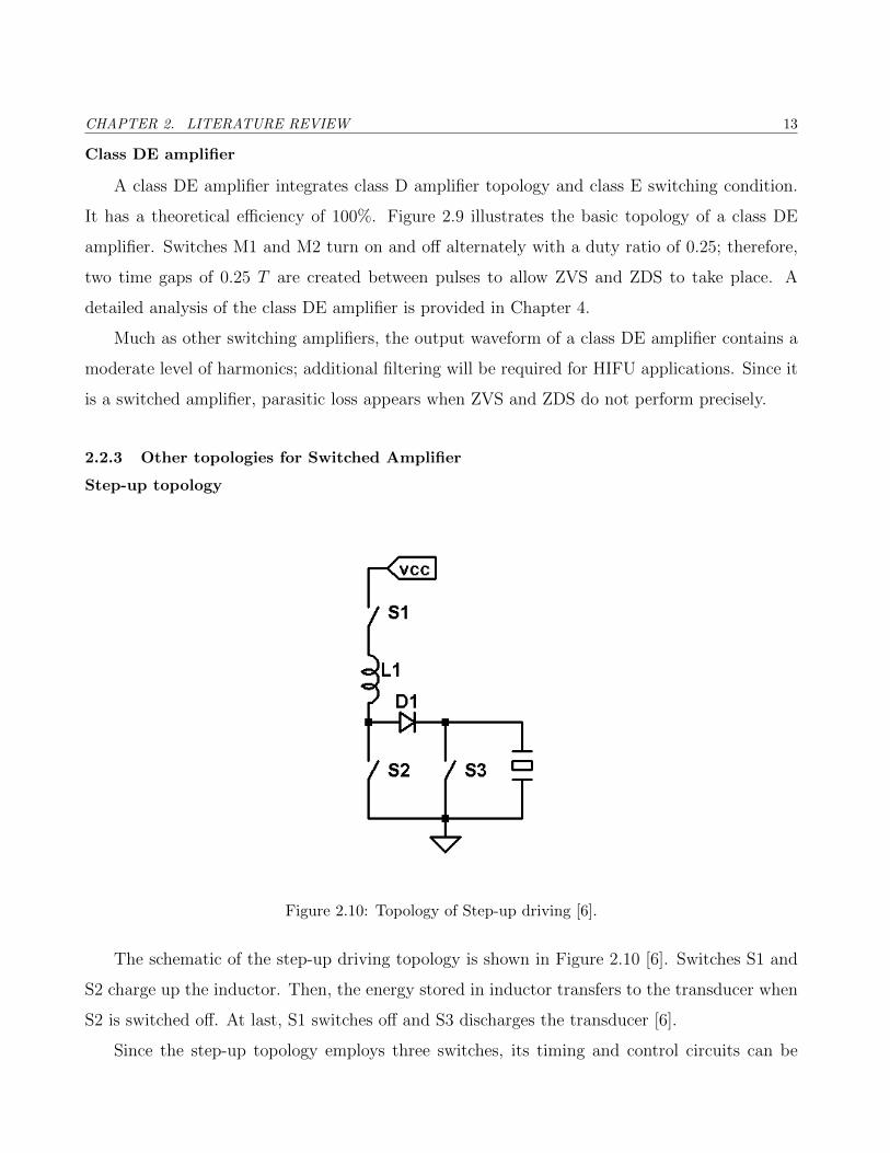
Step-up topology
Figure 2.10: Topology of Step-up driving [6].
The schematic of the step-up driving topology is shown in Figure 2.10 [6]. Switches S1 and
S2 charge up the inductor. Then, the energy stored in inductor transfers to the transducer when
S2 is switched off. At last, S1 switches off and S3 discharges the transducer [6].
Since the step-up topology employs three switches, its timing and control circuits can be

CHAPTER 2. LITERATURE REVIEW 14
very complicated. Moreover, diode D1 introduces additional losses.
Flyback topology
Figure 2.11: Topology of flyback driving [6].
The schematic of the flyback topology is shown in Figure 2.11. The primary winding of the
flyback transformer connects to the supply voltage and switch. By turning switch S1 on and off,
a high voltage is created at the terminal of S1. The secondary winding of transformer ties to
ground and transducer.
The major advantage of a flyback topology over other circuit topologies is that it needs only
one switch to generate signal pulses. However, the secondary winding and the static capacitor
of the transducer may create ringing [6].
Push-pull topology
The schematic of the push-pull topology is shown in Figure 2.12. The low voltage supply
ties to the central tap of transformer. Switches S1 and S2 connect to the primary winding of
transformer. Each switch turns on and off alternatively with a duty ratio of 0.5. The secondary
winding attaches to the transducer. The transformer is used for matching impedance of the
power supply and transducer to improve efficiency [6].
This topology is unsuitable for our design because it employs a transformer. Since the
integrated amplifier occupies an area of few millimeters, a transformer is too large for our appli-

CHAPTER 2. LITERATURE REVIEW 15
Figure 2.12: Topology of Push-pull driving [6].
cations.
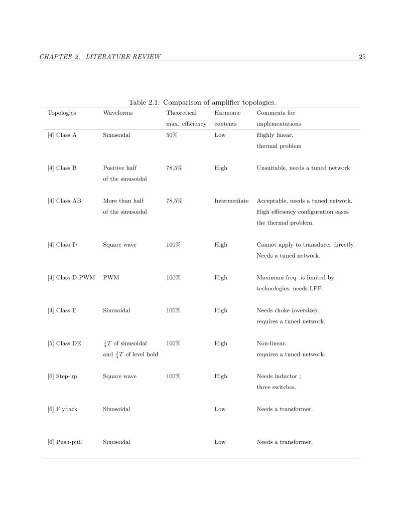
Table 2.1 on Page 25 summarizes the key features of the different types of amplifier introduced
in this section for comparison.
2.3 Review of Published Designs
The second half of this chapter dissertates the published amplifier topology for a piezoelectric
ultrasound transducer. Precedence of publications is organized chronologically.
Mizutani et al. [7] proposed a 60 W, 1 MHz DC-RF inverter that automatically tuned its
operating frequency to the resonant frequency of the transducer. The schematic is shown in
Figure 2.13. The purpose of implementing auto-tuning is to minimize the phase angle of output
voltage and current to the transducer so as to maintain a resistive output impedance. Current
sensing is implemented by feeding the current signal to a band pass filter and phase lock loop.
This is the flyback topology. It employs an output transformer and a current transformer.
As a result, it is not suitable for our design.
Agbossou et al. [8] proposed a 2 kW full bridge PWM class D power amplifier for driving a

CHAPTER 2. LITERATURE REVIEW 16
Figure 2.13: Schematic of DC to RF Inverter [7].
Figure 2.14: Schematic of class D inverter for piezoelectric transducer [8].

CHAPTER 2. LITERATURE REVIEW 17
Figure 2.15: Magnitude impedance of piezoelectric ultrasound transducer close to one of its resonant
frequencies. Variables fs and fp stand for series resonant frequency and parallel resonant frequency [8].
chemical reactor. The range of the operating frequency is between 10 kHz and 100 kHz and its
efficiency is greater than 90%. The topology of the proposed class D amplifier is shown in the
Figure 2.14. A LPF ensures that the load impedance seen by the amplifier is either resistive or
inductive.
The authors considered the impact on the amplifier performance due to the behaviour changes
of the piezoelectric load when the operating temperature of the transducer is changing. Fig-
ure 2.15 shows the magnitude impedance of a piezoelectric transducer near one of its resonant
frequency. If the operating frequency is equal to series resonant frequency, the impedance of the
piezoelectric load is purely resistive. Hence, the acoustic output of the transducer is maximized
because the phase shift between driving voltage waveform and current waveform is zero. Slight
variations of temperature will change the thickness of the piezoelectric resonator as well as its
behaviour. As shown in Figure 2.15, the impedance of a piezoelectric load is capacitive when
its operating frequency is below resonant frequency fs or above parallel resonant frequency fp.
Similarly, the impedance of a piezoelectric load is inductive when its operating frequency is be-
tween fs and fp. A RC snubber circuit and an anti-parallel diode are installed in parallel with
CHAPTER 2. LITERATURE REVIEW 18
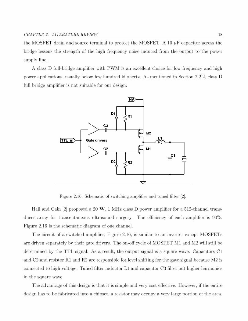
the MOSFET drain and source terminal to protect the MOSFET. A 10 µF capacitor across the
bridge lessens the strength of the high frequency noise induced from the output to the power
supply line.
A class D full-bridge amplifier with PWM is an excellent choice for low frequency and high
power applications, usually below few hundred kilohertz. As mentioned in Section 2.2.2, class D
full bridge amplifier is not suitable for our design.
Figure 2.16: Schematic of switching amplifier and tuned filter [2].
Hall and Cain [2] proposed a 20 W, 1 MHz class D power amplifier for a 512-channel trans-
ducer array for transcutaneous ultrasound surgery. The efficiency of each amplifier is 90%.
Figure 2.16 is the schematic diagram of one channel.
The circuit of a switched amplifier, Figure 2.16, is similar to an inverter except MOSFETs
are driven separately by their gate drivers. The on-off cycle of MOSFET M1 and M2 will still be
determined by the TTL signal. As a result, the output signal is a square wave. Capacitors C1
and C2 and resistor R1 and R2 are responsible for level shifting for the gate signal because M2 is
connected to high voltage. Tuned filter inductor L1 and capacitor C3 filter out higher harmonics
in the square wave.
The advantage of this design is that it is simple and very cost effective. However, if the entire
design has to be fabricated into a chipset, a resistor may occupy a very large portion of the area.
CHAPTER 2. LITERATURE REVIEW 19
Similarly, the inductor has to be off-chip.
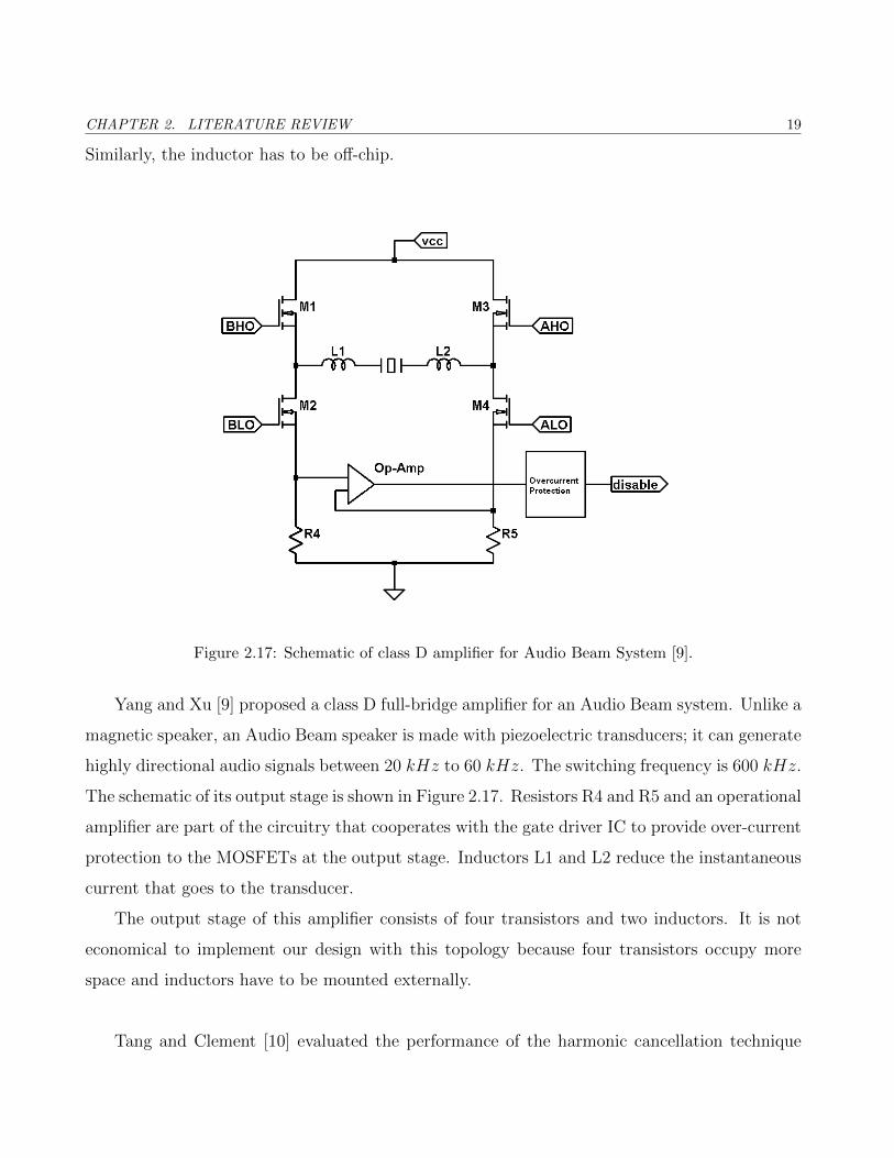
Figure 2.17: Schematic of class D amplifier for Audio Beam System [9].
Yang and Xu [9] proposed a class D full-bridge amplifier for an Audio Beam system. Unlike a
magnetic speaker, an Audio Beam speaker is made with piezoelectric transducers; it can generate
highly directional audio signals between 20 kHz to 60 kHz. The switching frequency is 600 kHz.
The schematic of its output stage is shown in Figure 2.17. Resistors R4 and R5 and an operational
amplifier are part of the circuitry that cooperates with the gate driver IC to provide over-current
protection to the MOSFETs at the output stage. Inductors L1 and L2 reduce the instantaneous
current that goes to the transducer.
The output stage of this amplifier consists of four transistors and two inductors. It is not
economical to implement our design with this topology because four transistors occupy more
space and inductors have to be mounted externally.
Tang and Clement [10] evaluated the performance of the harmonic cancellation technique
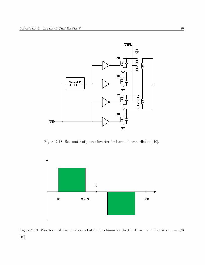
CHAPTER 2. LITERATURE REVIEW 20
Figure 2.18: Schematic of power inverter for harmonic cancellation [10].
Figure 2.19: Waveform of harmonic cancellation. It eliminates the third harmonic if variable a = π/3
[10].
CHAPTER 2. LITERATURE REVIEW 21
for a therapeutic ultrasound transducer in HIFU applications. The schematic of the amplifier is
shown in Figure 2.19. It comprises two power converters in cascade connection and the operating
frequency is 1 MHz.
In this work, the authors pointed out that driving an ultrasound piezoelectric transducer
with a signal that contains harmonics will distort the shape of the ultrasound focal spot. This is
because harmonic contents present in electrical signals cause the transducer to generate unwanted
sidelobes in the acoustic field. These sidelobes are carrying extra energy and will eventually dis-
tort the focal spot. The authors resolved this problem with the harmonic cancellation technique.
Harmonic cancellation is a technique that creates a square waveform with pre-calculated
firing angles to suppress particular harmonics. As shown in Figure 2.18, a square waveform, with
a firing angle of π/3 used as driving signal, eliminates the 3rd harmonic. The converter does not
require an additional LC filtering circuit; however, it employs two transformers. This technique
successfully attenuates the 3rd harmonic from -20 dB to -48 dB, comparing with the -46 dB at
the 5th harmonic. The mechanical characteristic of the transducer and electrical characteristics
of the coax cable can attenuate higher harmonic contents naturally.
Harmonic cancellation waveform must be very precise. Rise time and fall time should be min-
imal; otherwise, unwanted harmonics will appear at the output. In addition, it is not practical
to implement our design with this topology because the output stage comprises two transformers.
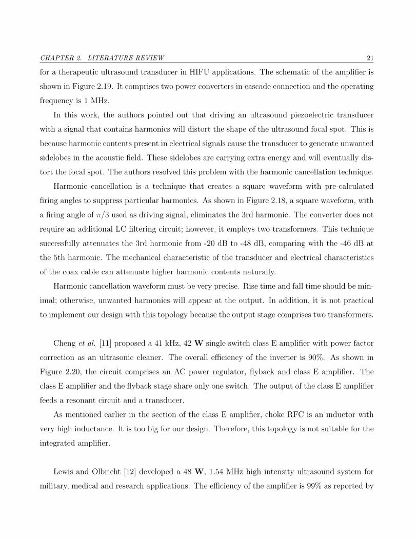
Cheng et al. [11] proposed a 41 kHz, 42 W single switch class E amplifier with power factor
correction as an ultrasonic cleaner. The overall efficiency of the inverter is 90%. As shown in
Figure 2.20, the circuit comprises an AC power regulator, flyback and class E amplifier. The
class E amplifier and the flyback stage share only one switch. The output of the class E amplifier
feeds a resonant circuit and a transducer.
As mentioned earlier in the section of the class E amplifier, choke RFC is an inductor with
very high inductance. It is too big for our design. Therefore, this topology is not suitable for the
integrated amplifier.
Lewis and Olbricht [12] developed a 48 W, 1.54 MHz high intensity ultrasound system for
military, medical and research applications. The efficiency of the amplifier is 99% as reported by
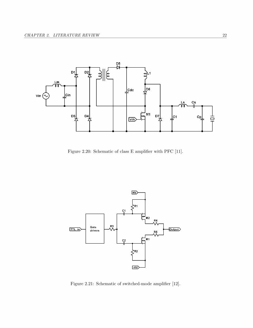
CHAPTER 2. LITERATURE REVIEW 22
Figure 2.20: Schematic of class E amplifier with PFC [11].
Figure 2.21: Schematic of switched-mode amplifier [12].
CHAPTER 2. LITERATURE REVIEW 23
the authors. Its schematic is shown in Figure 2.21. In order to achieve maximum power transfer
from a standard 50 Ohm power supply to a 50 Ohm transducer probe, the output impedance of
the amplifier must be as low as possible. The authors pointed out if 99% of the voltage from the
power supply must be transfered to load, the output impedance of the power amplifier should not
be greater than 0.05 Ohm. Their design was implemented using discrete components. Multiple
power transistors are connected in parallel with each other to achieve very low output impedance.
A RC network handles level shifting for MOSFETs. The overall design is lightweight, small in
size and cost effective. [12] Its topology is similar to [2] without a tuned LC harmonic filter
connecting between the amplifier output and transducer.
Since the driver is a class D amplifier, the output waveform of the amplifier is a square wave.
Driving an ultrasound transducer with a square wave will cause the acoustic pressure field to
contain harmonics; therefore this solution cannot be adapted to HIFU applications directly.
Figure 2.22: Schematic of output stage and matching network of LIPUS amplifier [13].
Low Intensity Pulsed Ultrasound, LIPUS, is an emerging technique that uses ultrasound for
CHAPTER 2. LITERATURE REVIEW 24
bone healing, dental tissue formation, and tooth-root healing. Ang et al. [13] had fabricated
a 0.8 W, 1.5 MHz integrated amplifier chip for LIPUS applications. Its schematic is shown in
Figure 2.22 and it was fabricated with DALSA 0.8 µm HV CMOS process. The overall efficiency
including a pulse generator and an amplifier is 70%.
Major challenges of LIPUS devices are portability and ultrasound transducer impedance
matching. First, the power amplifier and its signal generator are too large to fit for orthodontic
treatment. With the aid of advanced CMOS technologies, the authors successfully scaled down
both the pulse generator stage and the power output stage to a 2.8 mm × 4 mm chip. Sec-
ond, depending on the impedance characteristics of the piezoelectric resonator, an ultrasound
transducer usually requires high voltage and high current to produce enough acoustic power
for healing purposes. In order to mitigate the electrical requirements, an external tuned LC
matching network that matches impedance of the transducer at resonance frequency is inserted
in between the output of amplifier and the transducer. This LC filter boosts the output voltage
form 2.53 V peak to 7.6 V peak and eliminates higher harmonic contents from the output signals.
A level shifter was used as the power output stage as shown in Figure 2.22. The generation of
pulse modulated signals is done by a digital block.
Although this device was implemented as integrated circuit, it occupies an area of 2.8 mm×
4 mm and employs a matching network. In addition, in our case, an efficiency of 70% may create
thermal problems.
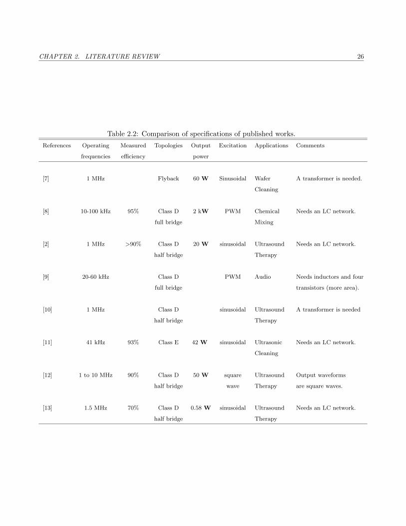
Table 2.2 summarizes the specifications and comments of all published works studied in this
section.
2.4 Summary
Although published works provide valuable information and techniques for designing piezo-
electric amplifiers, none of the published works offers an immediate solution to resolve our chal-
lenges, such as elimination of inductors. Hence, another approach is needed. Tables 2.1 and 2.2
are compendia of this chapter.
CHAPTER 2. LITERATURE REVIEW 25
Table 2.1: Comparison of amplifier topologies.
Topologies Waveforms Theoretical Harmonic Comments for
max. efficiency contents implementations
[4] Class A Sinusoidal 50% Low Highly linear,
thermal problem
[4] Class B Positive half 78.5% High Unsuitable, needs a tuned network
of the sinusoidal
[4] Class AB More than half 78.5% Intermediate Acceptable, needs a tuned network.
of the sinusoidal High efficiency configuration eases
the thermal problem.
[4] Class D Square wave 100% High Cannot apply to transducer directly.
Needs a tuned network.
[4] Class D PWM PWM 100% High Maximum freq. is limited by
technologies; needs LPF.
[4] Class E Sinusoidal 100% High Needs choke (oversize);
requires a tuned network.
[5] Class DE 14T of sinusoidal 100% High Non-linear,
and 14T of level hold requires a tuned network.
[6] Step-up Square wave 100% High Needs inductor ;
three switches.
[6] Flyback Sinusoidal Low Needs a transformer.
[6] Push-pull Sinusoidal Low Needs a transformer.
CHAPTER 2. LITERATURE REVIEW 26
Table 2.2: Comparison of specifications of published works.
References Operating Measured Topologies Output Excitation Applications Comments
frequencies efficiency power
[7] 1 MHz Flyback 60 W Sinusoidal Wafer A transformer is needed.
Cleaning
[8] 10-100 kHz 95% Class D 2 kW PWM Chemical Needs an LC network.
full bridge Mixing
[2] 1 MHz >90% Class D 20 W sinusoidal Ultrasound Needs an LC network.
half bridge Therapy
[9] 20-60 kHz Class D PWM Audio Needs inductors and four
full bridge transistors (more area).
[10] 1 MHz Class D sinusoidal Ultrasound A transformer is needed
half bridge Therapy
[11] 41 kHz 93% Class E 42 W sinusoidal Ultrasonic Needs an LC network.
Cleaning
[12] 1 to 10 MHz 90% Class D 50 W square Ultrasound Output waveforms
half bridge wave Therapy are square waves.
[13] 1.5 MHz 70% Class D 0.58 W sinusoidal Ultrasound Needs an LC network.
half bridge Therapy

Chapter 3
Characterisation of an Ultrasound
Transducer
3.1 Transducer
Figure 3.1: Exploded view of a transducer.
Ultrasound can be generated through a simple device called a transducer. Figure 3.1 shows an
exploded view of a therapy transducer [14]. The rightmost component is a piezoelectric resonator
that generates ultrasound. The schematic diagram of housing and assembly instructions of the

CHAPTER 3. CHARACTERISATION OF AN ULTRASOUND TRANSDUCER 28
ultrasound transducer can be found in Appendix A. For therapy transducers, the material of this
resonator is commonly made of Lead Zirconate Titanate, PZT. Electrodes are coated on both
sides of the resonator for electrical connections. The outer case is called the housing. It protects
both the internal circuitry and the piezoelectric resonator from the physical environment and
provides air backing for the resonator. Circuitry, such as a tuned filter and matching network,
can be mounted internally. A coax cable is used for signal transmission from the amplifier to the
piezoelectric resonator.
3.2 Equivalent Circuit
Figure 3.2: Equivalent circuit of a piezoelectric resonator near its resonance frequency [15].
The equivalent circuit of a piezoelectric resonator vibrating near its resonance is shown in
Figure 3.2 [15]. It comprises a capacitor connected in parallel with a series resonant circuit.
Mathematically, the impedance of equivalent circuit of Figure 3.2 can be expressed as follows:
Z =
1jωC0
(1
jωCS+RS + jωLS
)1
jωC0+ 1
jωCS+RS + jωLS
(3.1)
where ω is angular frequency; symbol j denotes√−1. The variable C0 is static capacitance that
represents the electrical branch of the resonator. It is determined by the physical properties
of the resonator, such as the permittivity with zero strain, surface area of the piezoelectric
resonator, and the distance between electrodes. The quantities Cs, Ls and Rs denote the series
resonant circuit that stands for the mechanical branch of the resonator, and Rs includes both
the mechanical losses and the mechanical power transferred to acoustic field. Terminals A and
B are inputs of the equivalent circuit. Usually, one of them is named HOT, and connects to the
output of amplifier or function generator. The other terminal is called Ground, which connects
to the earth or reference point of circuit.

CHAPTER 3. CHARACTERISATION OF AN ULTRASOUND TRANSDUCER 29
Figure 3.3: Impedance of equivalent circuit in Figure 3.2 [15].
The impedance of the equivalent circuit as a function of frequency is shown in Figure 3.3 [15].
The magnitude impedance of the equivalent circuit is denoted by | Z |, and Re(Z) and Im(Z)
are the real and imaginary components of the impedance Z; fp is parallel resonant frequency in
which the real part of the impedance Z reaches maximum; and fs is the series resonant frequency
when the reactance of the series resonant circuit Im(Z1) is zero, where Z1 = Rs + jωLs +1
jωCs.
When the equivalent circuit is operating at the resonant frequency, the reactance of Ls and Cs
cancel out each other, leaving only C0 parallel with Rs. For this reason, it is common to choose
an excitation frequency very close to the series resonant frequency, fs, as the operating frequency,
because the voltage can transfer to Rs directly. Therefore, the supply voltage will be minimal.
3.3 Mathematical Model
At series resonant frequency fs, the reactance of Ls and Cs cancel out each other. We simplify
Equation (3.1).
Zs|ω=ωs =
RsjωsC0
1jωsC0
+Rs
(3.2)
Formulae for Cs and Ls are provided in [15]:
Cs = C0
[(fpfs
)2
− 1
](3.3)
Ls =1
(2πfs)2Cs(3.4)
CHAPTER 3. CHARACTERISATION OF AN ULTRASOUND TRANSDUCER 30
Solving for C0 and Rs:
C0 =−Im(Zs)
2πfs|Zs|2(3.5)
RS =|Zs|2
Re(Zs)(3.6)
Equations 3.3 to 3.4 are applied at the fundamental frequency to calculate C0, Cs1, Ls1 and Rs1.
Once C0 is found; apply equations 3.4, 3.6 and 3.3 to find the LRC values for all remaining odd
harmonic branches. By connecting all odd harmonic branches with the fundamental branch in
parallel as shown in Figure 3.4 [14], an equivalent circuit of a multi-mode piezoelectric resonator
is found.
Figure 3.4: Equivalent circuit of a transducer [14].
The odd harmonics are a set of resonant frequencies based on the odd multiples of the
fundamental resonant frequency. They depend on the thickness and physical properties of the
piezoelectric material [14]. As shown in Figure 3.4 [14], the variable C0 denotes the static
capacitor. Components Ls1, Cs1, and Rs1 comprise the fundamental branch. Similarly, Ls3, Cs3,
and Rs3 represent the third harmonic branch, and so on.
In practice, however, more resonant frequencies can be found because a piezoelectric resonator
is a three dimensional object. These non-harmonic frequencies do not correspond to harmonics
or multiples of the fundamental frequency [14].
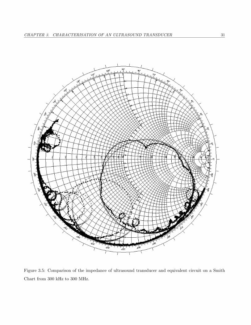
CHAPTER 3. CHARACTERISATION OF AN ULTRASOUND TRANSDUCER 31
Figure 3.5: Comparison of the impedance of ultrasound transducer and equivalent circuit on a Smith
Chart from 300 kHz to 300 MHz.
CHAPTER 3. CHARACTERISATION OF AN ULTRASOUND TRANSDUCER 32
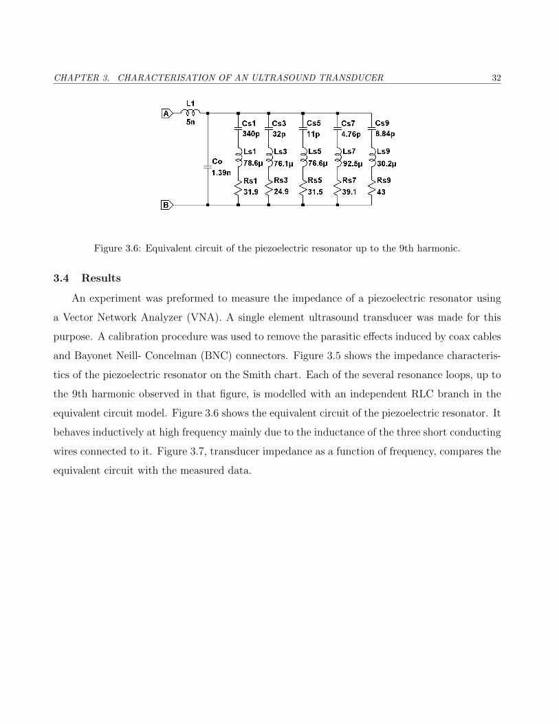
Figure 3.6: Equivalent circuit of the piezoelectric resonator up to the 9th harmonic.
3.4 Results
An experiment was preformed to measure the impedance of a piezoelectric resonator using
a Vector Network Analyzer (VNA). A single element ultrasound transducer was made for this
purpose. A calibration procedure was used to remove the parasitic effects induced by coax cables
and Bayonet Neill- Concelman (BNC) connectors. Figure 3.5 shows the impedance characteris-
tics of the piezoelectric resonator on the Smith chart. Each of the several resonance loops, up to
the 9th harmonic observed in that figure, is modelled with an independent RLC branch in the
equivalent circuit model. Figure 3.6 shows the equivalent circuit of the piezoelectric resonator. It
behaves inductively at high frequency mainly due to the inductance of the three short conducting
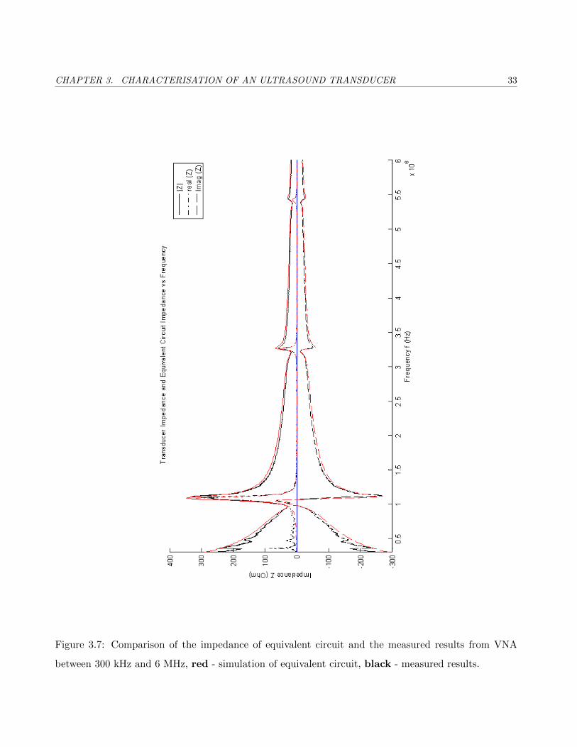
wires connected to it. Figure 3.7, transducer impedance as a function of frequency, compares the
equivalent circuit with the measured data.
CHAPTER 3. CHARACTERISATION OF AN ULTRASOUND TRANSDUCER 33
Figure 3.7: Comparison of the impedance of equivalent circuit and the measured results from VNA
between 300 kHz and 6 MHz, red - simulation of equivalent circuit, black - measured results.
CHAPTER 3. CHARACTERISATION OF AN ULTRASOUND TRANSDUCER 34
3.5 Ultrasound Field Characterization
Figure 3.8: Schematic diagram of the ultrasound field characterization using three-dimensional positing
system [14].
This section investigates the relation of the ratio of the electric fundamental to 3rd harmonic
and mechanical fundamental to 3rd harmonic. The mechanical attenuation between fundamental
and third harmonic are different. The goal is to predict the ratio of fundamental and 3rd harmonic
in ultrasound field with given electrical signals, such as the output signals of an amplifier.
The intensity of the ultrasound field can be measured through a wave field scan with a
three-dimensional positioning system. Figure 3.8 is a schematic of this system [14]. As shown
in the Figure 3.8, a power amplifier sends an RF signal to the transducer. On the right, a small
needle-like device called a hydrophone reads the acoustic pressure in front of the transducer.
The received signal is amplified by a pre-amplifier. A personal computer uses with the signal
generator and oscilloscope to record the position of the hydrophone, transmitted signals and
received signals. The water tank is filled with degassed and de-ionized water.
CHAPTER 3. CHARACTERISATION OF AN ULTRASOUND TRANSDUCER 35
Figure 3.9: Schematic diagram of a voltage source driving a transducer through a coax [16].
3.6 Calculations
Our goal is to derive an expression for the the voltage Vtdr that is applied to the piezoelectric
resonator. As shown in Figure 3.9 [16], RF signals are transmitted from the function generator
through a transmission line to the transducer. Variable l denotes the distance from the load;
voltage source Vg stands for the function generator; Zg denotes output impedance of the gener-
ator; Γ is the reflective coefficient of the transmission line; Ztdr represents the impedance of the
transducer. Zo and β stand for characteristic impedance and propagation constant respectively,
of the transmission line [16]. Beginning with the expression of voltage V (z) along a transmission
line, we have [16],
V (z) = V +(e−jβz + Γejβz) , (3.7)
where V (z) is the instantaneous voltage at any point along z-axis. Variable β is the propagation
constant of a transmission line, which is defined as
β = jω√LTL CTL , (3.8)
where LTL is the series inductance per unit length and and CTL is the shunt capacitance per unit
length of a transmission line. Angular frequency ω equals 2πf . The reflection coefficient Γ of a
transmission line is

CHAPTER 3. CHARACTERISATION OF AN ULTRASOUND TRANSDUCER 36
Γ =Ztdr − ZinZtdr + Zin
, (3.9)
where Ztdr is the impedance of the piezoelectric resonator. Variable Zin is the impedance reflected
from the coax, which is defined [16] as
Zin = Z0Ztdr + j Z0 tan(βl)
Z0 + j Ztdr tan(βl), (3.10)
where characteristic impedance Z0 of a transmission line is equal to
√LTLCTL
. Substituting z = −l
into equation (3.7), we have [16]
V (−l) = V +(ejβl + Γe−jβl) . (3.11)
Rearranging it, we have an expression of the incident voltage [16]
V + =V (−l)
(ejβl + Γe−jβl). (3.12)
At the input of the transmission line, z = −l, voltage V is expressed as [16]
V (−l) =Vg ZinZg + Zin
. (3.13)
Substituting z = 0 into equation (3.7), it becomes
V (0) =V +(1 + Γ) (3.14)
=V (−l)[
1
(ejβl + Γe−jβl)
][1 + Γ] (3.15)
Substituting V (−l) into the previous equation, we have an expression for the voltage V (0) at
the piezoelectric resonator.
Vtdr = V (0) =
[Vg ZinZg + Zin
] [1
(ejβl + Γe−jβl)
][1 + Γ] (3.16)
The attenuation between transmitted and received signals in dBV is given by
Attenuation (dBV ) = 20 log10
(VadjVtdr
), (3.17)
where voltage Vadj denotes the received signal, which was adjusted by the sensitivity of the
hydrophone. We also have
CHAPTER 3. CHARACTERISATION OF AN ULTRASOUND TRANSDUCER 37
Vadj = VhM(f = 1 MHz)
M(f). (3.18)
where M(f) is the sensitivity of the hydrophone corresponding to a particular frequency, and Vh
represents the measured results.
3.7 Results
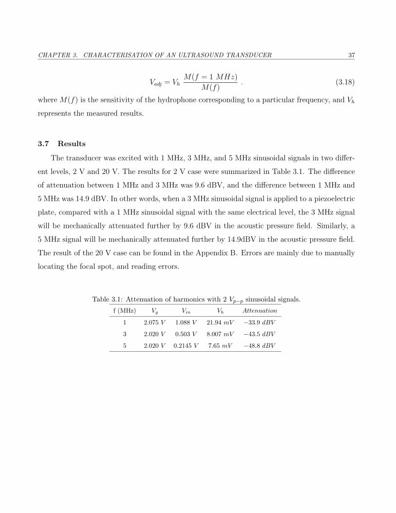
The transducer was excited with 1 MHz, 3 MHz, and 5 MHz sinusoidal signals in two differ-
ent levels, 2 V and 20 V. The results for 2 V case were summarized in Table 3.1. The difference
of attenuation between 1 MHz and 3 MHz was 9.6 dBV, and the difference between 1 MHz and
5 MHz was 14.9 dBV. In other words, when a 3 MHz sinusoidal signal is applied to a piezoelectric
plate, compared with a 1 MHz sinusoidal signal with the same electrical level, the 3 MHz signal
will be mechanically attenuated further by 9.6 dBV in the acoustic pressure field. Similarly, a
5 MHz signal will be mechanically attenuated further by 14.9dBV in the acoustic pressure field.
The result of the 20 V case can be found in the Appendix B. Errors are mainly due to manually
locating the focal spot, and reading errors.
Table 3.1: Attenuation of harmonics with 2 Vp−p sinusoidal signals.
f (MHz) Vg Vin Vh Attenuation
1 2.075 V 1.088 V 21.94 mV −33.9 dBV
3 2.020 V 0.503 V 8.007 mV −43.5 dBV
5 2.020 V 0.2145 V 7.65 mV −48.8 dBV
Chapter 4
Amplifier Design
4.1 Introduction
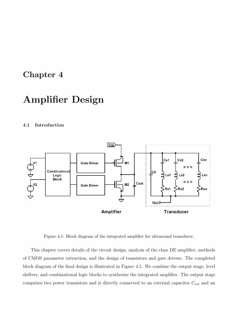
Figure 4.1: Block diagram of the integrated amplifier for ultrasound transducer.
This chapter covers details of the circuit design, analysis of the class DE amplifier, methods
of CMOS parameter extraction, and the design of transistors and gate drivers. The completed
block diagram of the final design is illustrated in Figure 4.1. We combine the output stage, level
shifters, and combinational logic blocks to synthesize the integrated amplifier. The output stage
comprises two power transistors and is directly connected to an external capacitor Cext and an
CHAPTER 4. AMPLIFIER DESIGN 39
ultrasound transducer. The extra capacitance provided by Cext stabilizes the behaviour of the
transducer observed from the amplifier when the transducer is subjected to thermal expansion
[13]. The gate driver comprises a level shifter and an output stage to produce a 20 V swing. A
combinational logic circuit block is located prior to the gate drivers and is responsible for power
stage on-off functioning and faulty signal filtering. Sources v1 and v2 are signal generators. This
design has been simulated with Spectre R©, a circuit simulator, part of Cadence R© software suite
for professional custom IC design and validation.
A class DE amplifier was used for the integrated amplifier because it can be used in high
frequency applications [17]. It is efficient and (in this case) does not require inductors. The
performance of a class D amplifier at high frequencies can be improved with ZVS and ZDS. By
reducing the turn-on ratio D of each transistor from 0.5 to 0.25, it allows the network to precisely
discharge the shunt capacitor before the next transistor conducts. This idea has been established
for class DE amplifiers and will be described in Section 4.2.
4.1.1 CMOS process kit
The design is implemented with the 0.8µm CMOS process 5/20 V kit offered by Teledyne-
DALSA Semiconductor. It allows both standard 5 V and 20 V transistors to be fabricated in the
same die. Complementary middle voltage transistors permit users to create a compact design,
integrating a high power output driver and taking advantage of complementary circuit topologies
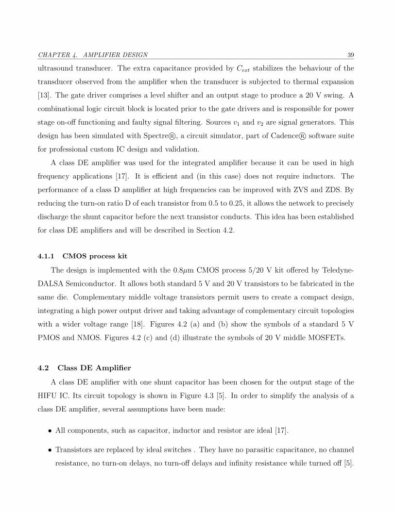
with a wider voltage range [18]. Figures 4.2 (a) and (b) show the symbols of a standard 5 V
PMOS and NMOS. Figures 4.2 (c) and (d) illustrate the symbols of 20 V middle MOSFETs.
4.2 Class DE Amplifier
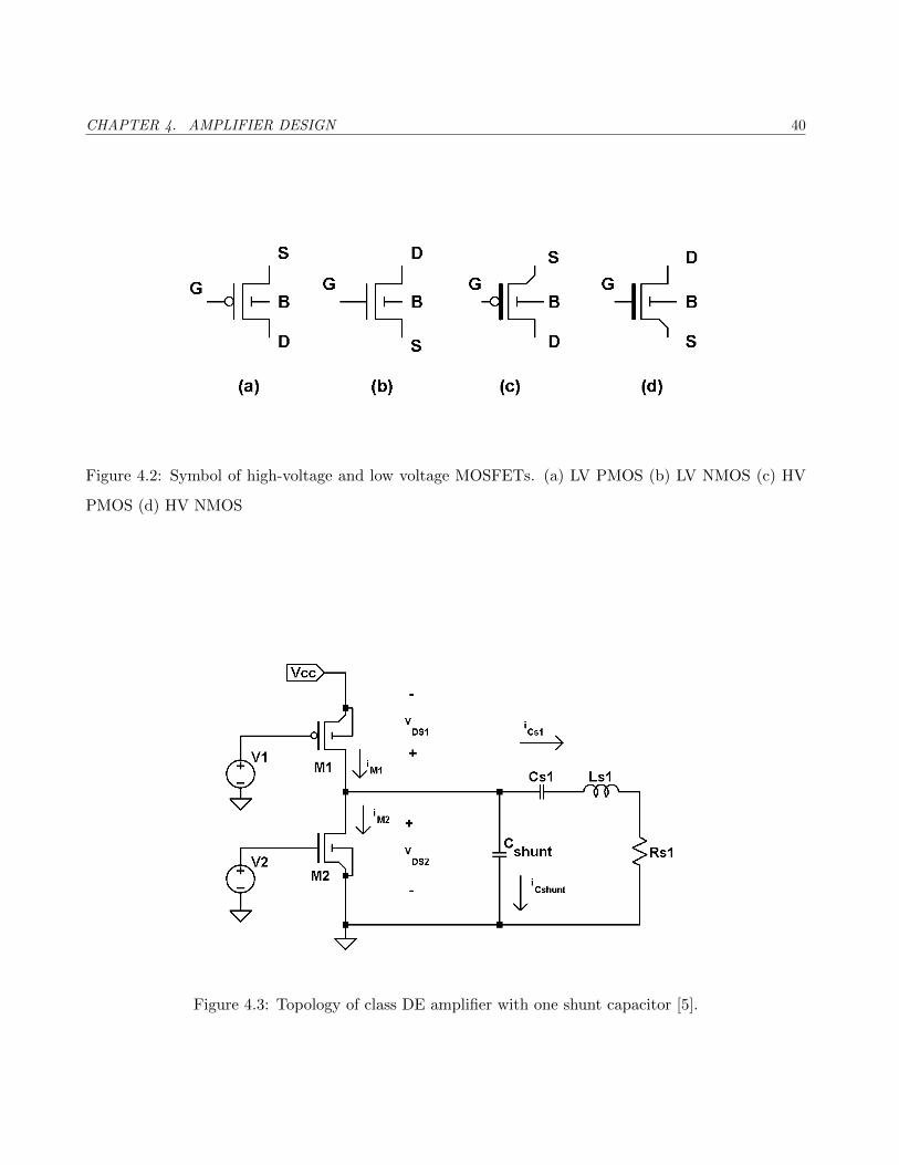
A class DE amplifier with one shunt capacitor has been chosen for the output stage of the
HIFU IC. Its circuit topology is shown in Figure 4.3 [5]. In order to simplify the analysis of a
class DE amplifier, several assumptions have been made:
• All components, such as capacitor, inductor and resistor are ideal [17].
• Transistors are replaced by ideal switches . They have no parasitic capacitance, no channel
resistance, no turn-on delays, no turn-off delays and infinity resistance while turned off [5].
CHAPTER 4. AMPLIFIER DESIGN 40
Figure 4.2: Symbol of high-voltage and low voltage MOSFETs. (a) LV PMOS (b) LV NMOS (c) HV
PMOS (d) HV NMOS
Figure 4.3: Topology of class DE amplifier with one shunt capacitor [5].
CHAPTER 4. AMPLIFIER DESIGN 41
Figure 4.4: Voltage waveforms of class DE amplifier [5]. (a) and (b) The switch-on timing diagram of
switches M1 and M2. (c) and (d) The voltage waveforms of switches M1 and M2. They are represented
by symbols vDS1 and vDS2 respectively.
CHAPTER 4. AMPLIFIER DESIGN 42
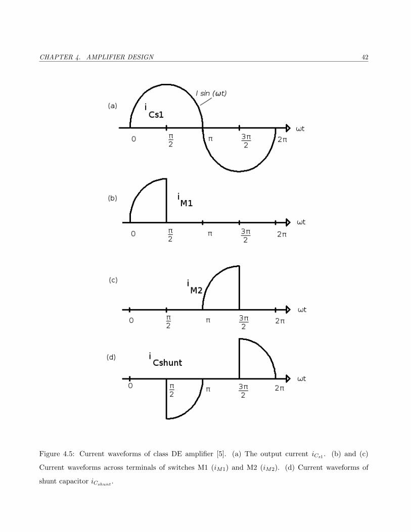
Figure 4.5: Current waveforms of class DE amplifier [5]. (a) The output current iCs1 . (b) and (c)
Current waveforms across terminals of switches M1 (iM1) and M2 (iM2). (d) Current waveforms of
shunt capacitor iCshunt .

CHAPTER 4. AMPLIFIER DESIGN 43
• The quality factor Q =ωLs1Rs1
of the load network is more than 2.5 [5], high enough to
produce a sinusoidal output current iCs1 .
• The switch-on duty ratio (D) is exactly one quarter of a period of the operating frequency
[5], [19], [20]. Variable D is the ratio of switch’s conducting time to its period of working
frequency: D =Ton
T. Period T and switch-on duration TON are illustrated in Figure 4.4
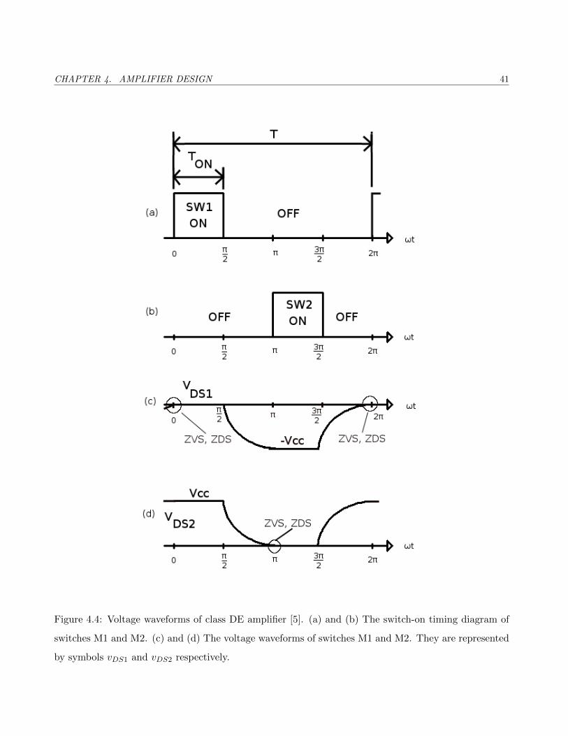
(a). Each switch is manipulated by an ideal source.
Based on these assumptions, voltage waveforms, current waveforms and equivalent circuits are
constructed and illustrated in Figure 4.4, Figure 4.5 and Figure 4.6 [5]. At any time, the output
current iCs1 can be expressed as
iCs1(ωt) = I sin(ωt+ φ) (4.1)
where I = V ccRS1
is the amplitude of current that flows through the series resonant network; φ is
phase shift; ω is the angular frequency and variable t denotes time. Since the iCs1 curve goes
through zero at ωt = π, the phase angle φ is 0. Thus, the expression for output current becomes
iCs1 = I sin(ωt) (4.2)
The operation of a class DE amplifier in steady state can be divided into four intervals. Fig-
ure 4.6 illustrates the corresponding equivalent circuit in each period.
Interval 1, between 0 radians andπ
2. Switch M1 conducts; Switch M2 is turned off. The
equivalent circuit is shown in Figure 4.6(a). Current iM1 (Figure 4.5(a) ) slowly rises from zero
at 0 radians and reaches its peak atπ
2. Terminals of switch M2 are at the same potential (V cc)
during this period; therefore, no current will flow through capacitor Cshunt. Current iM1 becomes
the only source that feeds the series resonant network. Before 0 radians, voltage across switch
M1 vDS1(ωt) is increasing. It eventually reaches the ground potential at 0 radians. At the same
instance, switch M1 is turned on. Since both of its terminals are at the ground potential, the
switching losses is zero (ZVS). The derivative of vDS1(ωt) is also zero at this point (ZVD).
The advantage of achieving ZVC and ZDS is to eliminate switching losses while the switch is
turned on.
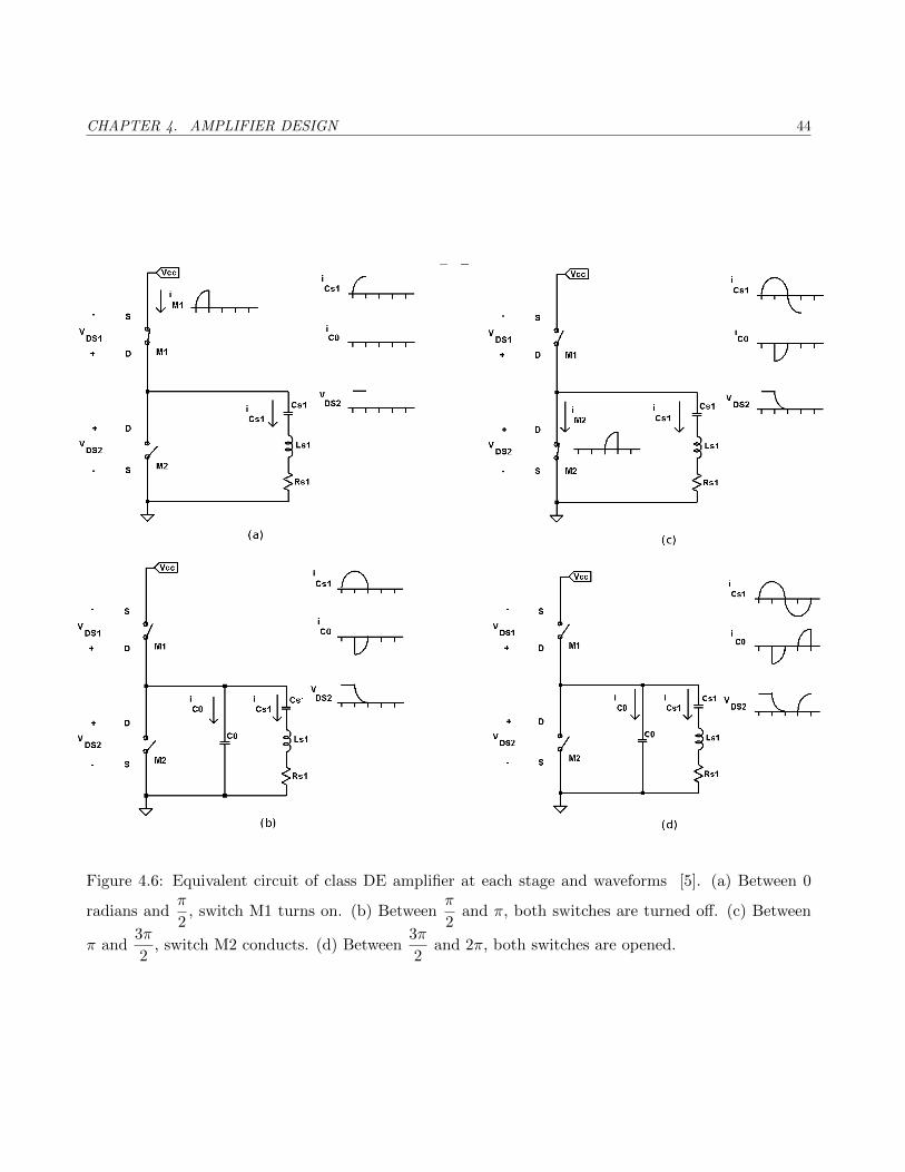
CHAPTER 4. AMPLIFIER DESIGN 44
Figure 4.6: Equivalent circuit of class DE amplifier at each stage and waveforms [5]. (a) Between 0
radians andπ
2, switch M1 turns on. (b) Between
π
2and π, both switches are turned off. (c) Between
π and3π
2, switch M2 conducts. (d) Between
3π
2and 2π, both switches are opened.
CHAPTER 4. AMPLIFIER DESIGN 45
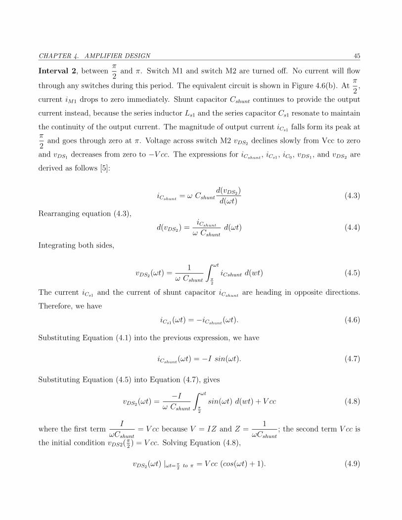
Interval 2, betweenπ
2and π. Switch M1 and switch M2 are turned off. No current will flow
through any switches during this period. The equivalent circuit is shown in Figure 4.6(b). Atπ
2,
current iM1 drops to zero immediately. Shunt capacitor Cshunt continues to provide the output
current instead, because the series inductor Ls1 and the series capacitor Cs1 resonate to maintain
the continuity of the output current. The magnitude of output current iCs1 falls form its peak atπ
2and goes through zero at π. Voltage across switch M2 vDS2 declines slowly from Vcc to zero
and vDS1 decreases from zero to −V cc. The expressions for iCshunt , iCs1 , iC0 , vDS1 , and vDS2 are
derived as follows [5]:
iCshunt = ω Cshuntd(vDS2)
d(ωt)(4.3)
Rearranging equation (4.3),
d(vDS2) =iCshuntω Cshunt
d(ωt) (4.4)
Integrating both sides,
vDS2(ωt) =1
ω Cshunt
∫ ωt
π2
iCshunt d(wt) (4.5)
The current iCs1 and the current of shunt capacitor iCshunt are heading in opposite directions.
Therefore, we have
iCs1(ωt) = −iCshunt(ωt). (4.6)
Substituting Equation (4.1) into the previous expression, we have
iCshunt(ωt) = −I sin(ωt). (4.7)
Substituting Equation (4.5) into Equation (4.7), gives
vDS2(ωt) =−I
ω Cshunt
∫ ωt
π2
sin(ωt) d(wt) + V cc (4.8)
where the first termI
ωCshunt= V cc because V = IZ and Z =
1
ωCshunt; the second term V cc is
the initial condition vDS2(π2) = V cc. Solving Equation (4.8),
vDS2(ωt) |ωt=π2to π = V cc (cos(ωt) + 1). (4.9)
CHAPTER 4. AMPLIFIER DESIGN 46
The voltage across switch M1, vDS1(ωt) is
vDS1(ωt) = vDS2(ωt)− V cc. (4.10)
Substituting Equation (4.9) into previous equation gives
vDS1(ωt) |ωt=π2to π = V cc (cos(ωt)) (4.11)
Interval 3, between π and3π
2. Switch M1 remains opened. The equivalent circuit is shown
in Figure 4.6(c). Voltage vDS1(ωt) is maintained at -Vcc. At π, Switch M2 conducts with no
potential difference between its terminals; this satisfies the conditions of ZVS and ZDS. The
output current iC0 goes through zero and keeps decreasing. At3π
2, ic0 reaches −I. Since M2 is
conducting, no current flows through the shunt capacitor. Table 4.1 summarize the conditions
of ZVS and ZDS for M1 and M2 [5].
Table 4.1: Conditions of ZVS and ZDS.
Switch M1 Switch M2
ZVS vDS1(2π) = 0 vDS2(π) = 0
ZDSd(vDS1(2π))
d(ωt)= 0
d(vDS2(π))
d(ωt)= 0
Interval 4, between3π
2and 2π. Both switches are closed. The equivalent circuit is illustrated
in Figure 4.6(d). At3π
2, the shunt capacitor C0 sources the output current, because Cs1 and
Ls1 are resonating. Current iCs1 declines to zero at 2π. During this period, voltage vDS1(ωt)
increases slowly from −V cc to zero and voltage vDS2(ωt) increases from zero to V cc. Following
a similar derivation as for Interval 2, expressions for vDS1(ωt) and vDS2(ωt) are:
vDS2(ωt) |ωt= 2π2to 2π= V cc (cos(ωt)) (4.12)
and
vDS1(ωt) |ωt= 2π2to 2π= V cc (cos(ωt)− 1). (4.13)
CHAPTER 4. AMPLIFIER DESIGN 47
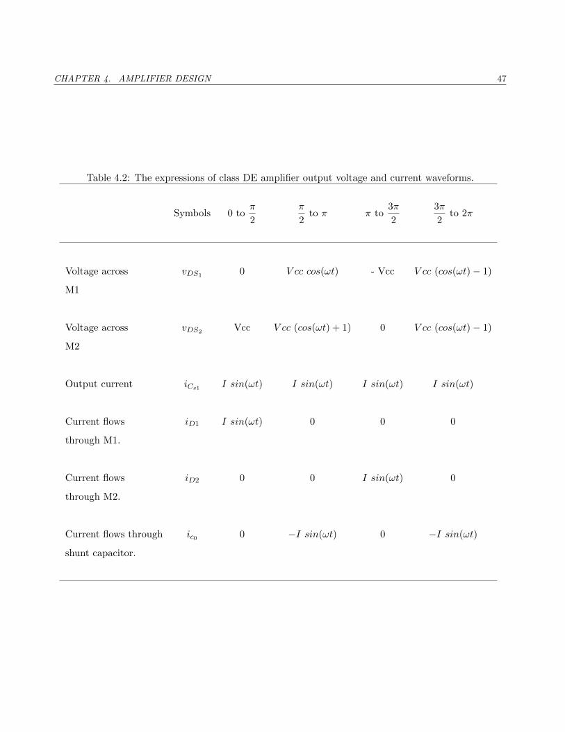
Table 4.2: The expressions of class DE amplifier output voltage and current waveforms.
Symbols 0 toπ
2
π
2to π π to
3π
2
3π
2to 2π
Voltage across vDS1 0 V cc cos(ωt) - Vcc V cc (cos(ωt)− 1)
M1
Voltage across vDS2 Vcc V cc (cos(ωt) + 1) 0 V cc (cos(ωt)− 1)
M2
Output current iCs1 I sin(ωt) I sin(ωt) I sin(ωt) I sin(ωt)
Current flows iD1 I sin(ωt) 0 0 0
through M1.
Current flows iD2 0 0 I sin(ωt) 0
through M2.
Current flows through ic0 0 −I sin(ωt) 0 −I sin(ωt)
shunt capacitor.
CHAPTER 4. AMPLIFIER DESIGN 48
It is important to point out that this analysis only considers an ideal scenario that excludes
real parameters such as parasitic capacitance, channel resistance, and switching delays. In the
circuit design, drain capacitance should be estimated because it directly affects the switching
conditions. It will add up to the shunt capacitance to form a total capacitance in calculations.
Moreover, capacitance is considered to be a constant while voltage is varying. Other factors such
as channel resistance, and turn-on and turn-off delays are inevitable in reality. The measured
efficiency of class DE amplifiers in references [17, 19] is above 90 % operating at 1 MHz with
an output power between 1 W and 7 W. Losses are mainly due to switching losses and parasitic
resistance [20]. Table 4.2 summarizes all expressions valid in each interval.
4.2.1 Tuning of a practical class DE amplifier
Since the class DE amplifier attaches to an ultrasound transducer instead of a designated
load network, it will not function in ideal mode. In such a case, tuning will help designers to
discover the best configuration, a combination of D and Cshunt, without jeopardizing too many
of the design requirements, such as efficiency, output power and low harmonics. Spectre R©, a
circuit simulator in the Cadence R© suite, carried this out with the parametric analysis.
Ablulet [19] recommended a tuning procedure for the class DE amplifier. It involves vary-
ing circuit parameters including switch-on duty ratio D, inductance Ls1, and capacitance Cs1.
The author claimed that a practical class DE amplifier will not operate in optimum condi-
tion once built. Instead, by varying D and phase angle ψ of the series resonant network, the
best possible working condition can be obtained through analysis. The equation of phase angle
ψ = arctan( 1Rs1
(2πf Ls1− 12πf Cs1
)) implied that φ can be adjusted by series capacitance Cs1 and
inductance Ls1 [19] in Figure 4.3. The range of D can be anywhere from 0.25 to 0.5. Figure 4.7
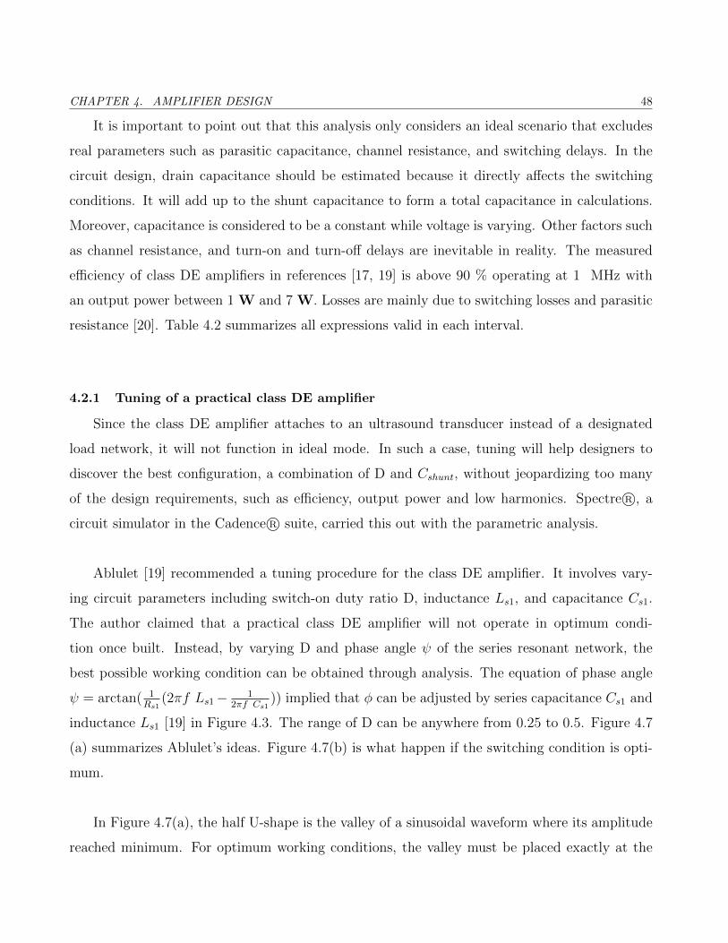
(a) summarizes Ablulet’s ideas. Figure 4.7(b) is what happen if the switching condition is opti-
mum.
In Figure 4.7(a), the half U-shape is the valley of a sinusoidal waveform where its amplitude
reached minimum. For optimum working conditions, the valley must be placed exactly at the
CHAPTER 4. AMPLIFIER DESIGN 49
Figure 4.7: Tuning procedure for class DE amplifier [19]. (a) Tuning procedure (b) Optimum condition.
intersection of the boundary of on-off region (the vertical dotted line in Figure 4.7) and the hori-
zontal axis ωt. To move the circle along the left diagonal, the phase angle should be varied. The
phase angle is equal to the arctan of the residual reactance of capacitance Cs and inductance Ls
divided by resistance Rs. On the other hand, for the trough travelling along the right diagonal,
D should be varied. Decreasing D moves the trough to the lower left hand corner, and vice versa.
The author concluded that, unlike a class E amplifier, it is nearly impossible for a class DE
amplifier to achieve very precise switching operations with real components. The practical range
of D is between 0.25 and 0.33 [19]. In addition, the optimum point of class DE power amplifier
does not occur at maximum output or input [19]. The above analysis is limited to a constant
output capacitance scenario.
CHAPTER 4. AMPLIFIER DESIGN 50
4.2.2 Calculations
External Capacitance for class DE amplifier
As shown in Figure 4.1, the output network of the class DE amplifier is composed of an
ultrasound transducer connecting in parallel with an external capacitor (Cext). The magnitude
of shunt capacitance should be determined because it determines the reasonable external ca-
pacitance that should be used in tuning. The expression of the shunt capacitance is derived as
follows [5]:
IDC =1
2π
∫ π2
0
iRs1 d(ωt)
=1
2π
∫ π2
0
Im sin(ωt) d(ωt)
=Im2π
=V cc ω Cshunt
2π
where IDC stands for DC input current and Im denotes the peak magnitude of sinusoidal current.
The peak voltage across Rs1 is derived using Fourier analysis [5]:
Vm =1
π
∫ 2π
0
vDS2 sin (ωt) d(ωt)
=1
π[
∫ π2
0
V cc sin(ωt) d(wt) +
∫ π
π2
V cc (cos(ωt) + 1) sin(ωt) d(wt) + · · ·
+
∫ 2π
3π2
V cc cos(ωt) sin(ωt) d(wt)]
=1
π
[V cc+
V cc
2− V cc
2
]=V cc
π
Assuming 100% efficiency, the power of DC supply is completely transferred to the load resistor
[5]:
P =Vm
2
2Rs1
=
(V cc
π
)21
2Rs1
= V cc IDC = V cc
(V cc ω Cshunt
2π
), (4.14)
where P stands for power. Simplify the above expression; we have,
Cshunt =1
π ω Rs1
(4.15)

CHAPTER 4. AMPLIFIER DESIGN 51
where ω = 2πfs is the series resonant frequency of the fundamental branch; Rs1 is the resistor
of the fundamental branch [5]. In this case, the external capacitor Cext is given by:
Cext = Cshunt − C0 − CdrainM1− CdrainM2
(4.16)
Cext =1
π (2π fs) Rs1
− C0 − CdrainM1− CdrainM2
, (4.17)
where variable C0 is the transducer′s static capacitor. Variables CdrainM1and CdrainM2
denote
the drain capacitance of the power MOSFETs M1 and M2.
Drain Capacitance of a MOSFET
The drain capacitance of a MOSFET can be estimated as follows.
Cdrain = (Ldrain ·W ) · cj + 2(W + Ldrain) · cjsw , (4.18)
where variable W denotes the width of a MOSFET gate, and Ldrain is the length of drain;
process parameters cj and cjsw denote junction capacitance and junction sidewall capacitance
respectively. Since all process parameters use in simulation model are confidential, we can only
provide the results here. The estimated drain capacitance of M1 and M2 were 18.43 pF and
24.31 pF respectively. Substituting them into (4.17) gives
Cext =1
π (2π) ( 0.982 MHz) (31.88Ω)− 1.388 nF − 18.43 pF − 24.31 pF
= 273 pF
Gate Capacitance of a MOSFET
The gate capacitance of a MOSFET can be estimated as follows.
Cgate = W · L · cox+W (cgdo+ cgso) (4.19)
where Cgate is the gate capacitance; process parameters cgdo denotes gate-drain parasitic ca-
pacitance and cgso represents gate-source parasitic capacitance. The variable Cox is defined as
follows.
Cox =ε0εrtox
(4.20)
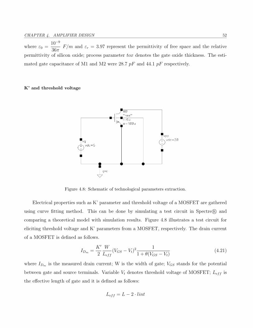
CHAPTER 4. AMPLIFIER DESIGN 52
where ε0 =10−9
36πF/m and εr = 3.97 represent the permittivity of free space and the relative
permittivity of silicon oxide; process parameter tox denotes the gate oxide thickness. The esti-
mated gate capacitance of M1 and M2 were 28.7 pF and 44.1 pF respectively.
K’ and threshold voltage
Figure 4.8: Schematic of technological parameters extraction.
Electrical properties such as K’ parameter and threshold voltage of a MOSFET are gathered
using curve fitting method. This can be done by simulating a test circuit in Spectre R© and
comparing a theoretical model with simulation results. Figure 4.8 illustrates a test circuit for
eliciting threshold voltage and K’ parameters from a MOSFET, respectively. The drain current
of a MOSFET is defined as follows.
IDm =K ′
2
W
Leff(VGS − Vt)2
1
1 + θ(VGS − Vt)(4.21)
where IDm is the measured drain current; W is the width of gate; VGS stands for the potential
between gate and source terminals. Variable Vt denotes threshold voltage of MOSFET; Leff is
the effective length of gate and it is defined as follows:
Leff = L− 2 · lint
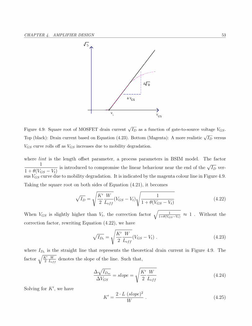
CHAPTER 4. AMPLIFIER DESIGN 53
Figure 4.9: Square root of MOSFET drain current√ID as a function of gate-to-source voltage VGS .
Top (black): Drain current based on Equation (4.23). Bottom (Magenta): A more realistic√ID versus
VGS curve rolls off as VGS increases due to mobility degradation.
where lint is the length offset parameter, a process parameters in BSIM model. The factor1
1 + θ(VGS − Vt)is introduced to compromise the linear behaviour near the end of the
√ID ver-
sus VGS curve due to mobility degradation. It is indicated by the magenta colour line in Figure 4.9.
Taking the square root on both sides of Equation (4.21), it becomes
√ID =
√K ′
2
W
Leff(VGS − Vt)
√1
1 + θ(VGS − Vt)(4.22)
When VGS is slightly higher than Vt, the correction factor√
11+θ(VGS−Vt)
≈ 1 . Without the
correction factor, rewriting Equation (4.22), we have
√IDt =
√K ′
2
W
Leff(VGS − Vt) . (4.23)
where IDt is the straight line that represents the theoretical drain current in Figure 4.9. The
factor√
K′
2WLeff
denotes the slope of the line. Such that,
∆√IDm
∆VGS= slope =
√K ′
2
W
Leff(4.24)
Solving for K ′, we have
K ′ =2 · L (slope)2
W. (4.25)
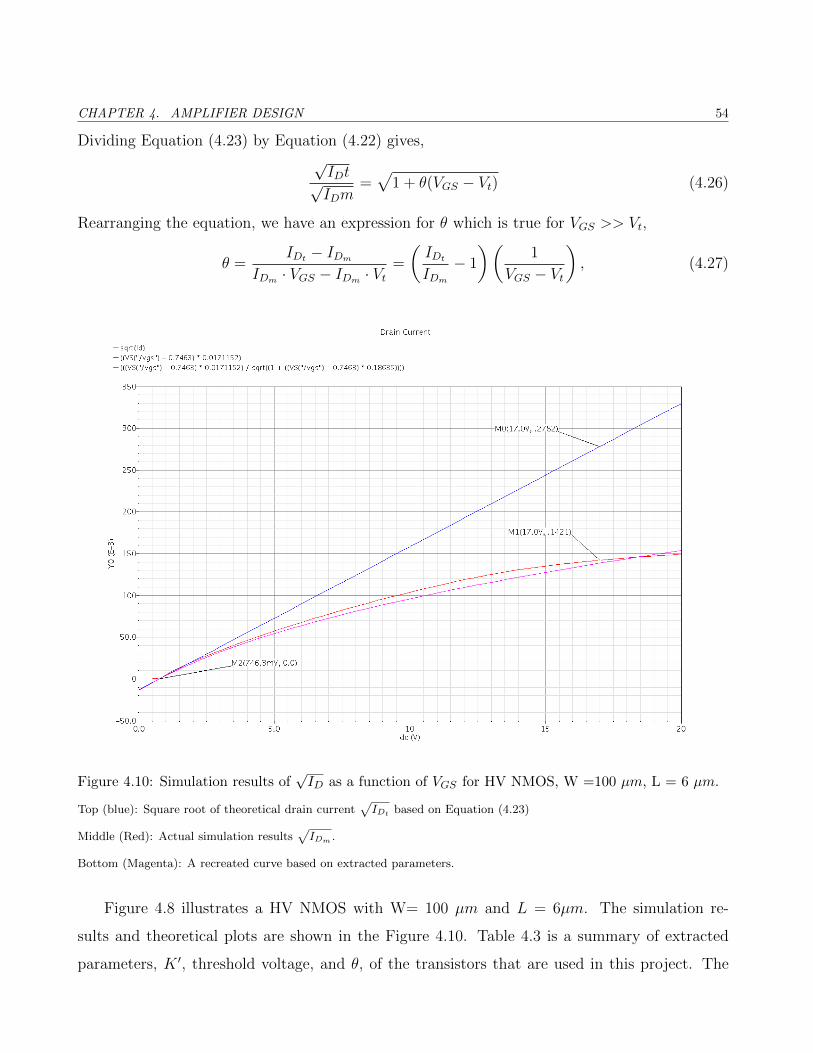
CHAPTER 4. AMPLIFIER DESIGN 54
Dividing Equation (4.23) by Equation (4.22) gives,√IDt√IDm
=√
1 + θ(VGS − Vt) (4.26)
Rearranging the equation, we have an expression for θ which is true for VGS >> Vt,
θ =IDt − IDm
IDm · VGS − IDm · Vt=
(IDtIDm− 1
)(1
VGS − Vt
), (4.27)
Figure 4.10: Simulation results of√ID as a function of VGS for HV NMOS, W =100 µm, L = 6 µm.
Top (blue): Square root of theoretical drain current√IDt based on Equation (4.23)
Middle (Red): Actual simulation results√IDm .
Bottom (Magenta): A recreated curve based on extracted parameters.
Figure 4.8 illustrates a HV NMOS with W= 100 µm and L = 6µm. The simulation re-
sults and theoretical plots are shown in the Figure 4.10. Table 4.3 is a summary of extracted
parameters, K ′, threshold voltage, and θ, of the transistors that are used in this project. The
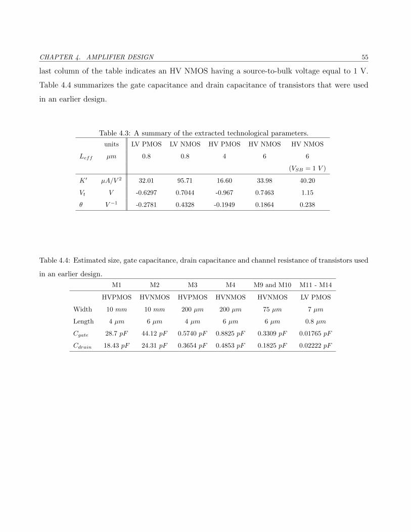
CHAPTER 4. AMPLIFIER DESIGN 55
last column of the table indicates an HV NMOS having a source-to-bulk voltage equal to 1 V.
Table 4.4 summarizes the gate capacitance and drain capacitance of transistors that were used
in an earlier design.
Table 4.3: A summary of the extracted technological parameters.
units LV PMOS LV NMOS HV PMOS HV NMOS HV NMOS
Leff µm 0.8 0.8 4 6 6
(VSB = 1 V )
K ′ µA/V 2 32.01 95.71 16.60 33.98 40.20
Vt V -0.6297 0.7044 -0.967 0.7463 1.15
θ V −1 -0.2781 0.4328 -0.1949 0.1864 0.238
Table 4.4: Estimated size, gate capacitance, drain capacitance and channel resistance of transistors used
in an earlier design.
M1 M2 M3 M4 M9 and M10 M11 - M14
HVPMOS HVNMOS HVPMOS HVNMOS HVNMOS LV PMOS
Width 10 mm 10 mm 200 µm 200 µm 75 µm 7 µm
Length 4 µm 6 µm 4 µm 6 µm 6 µm 0.8 µm
Cgate 28.7 pF 44.12 pF 0.5740 pF 0.8825 pF 0.3309 pF 0.01765 pF
Cdrain 18.43 pF 24.31 pF 0.3654 pF 0.4853 pF 0.1825 pF 0.02222 pF
CHAPTER 4. AMPLIFIER DESIGN 56
Channel Resistance of MOSFET
The channel resistance of both power transistors should be confirmed to be the same under iden-
tical biasing conditions. The expression of channel resistance can be derived from the expression
of drain current of a MOSFET operated in triode mode.
ID =K ′
2
W
Leff
[2 (VGS − Vt) VDS − VDS2]1 + θ (VGS − Vt)
(4.28)
While the channel is fully opened, VDS is much less than 2(VGS − Vt). Therefore, the expres-
sion (4.28) becomes
ID ≈K ′
2
W
Leff
[2 (VGS − Vt) VDS]
1 + θ (VGS − Vt).
Rearranging it, we have the expression of the channel resistance.
Rch =VDSID
=1 + θ (VGS − Vt)K ′
2
W
Leff(VGS − Vt)
. (4.29)
The estimated channel resistance of M1 and M2 were respectively 4.17 Ω and 4.07 Ω . The
simulated channel resistance of both M1 and M2 were 3.41 Ω and 3.39 Ω correspondingly.
4.3 Gate Driver
The gate driver, converting 5 V digital signals to 20 V gate signals, comprises a level shifter
and an output stage. Its schematic is illustrated in Figure 4.11 [21]. It requires two supply volt-
ages of 5 V (V dd) and 20 V (V pp) respectively. The output stage consists of two high-voltage
transistors M3 and M4, with the gate of the M3 routed to the level shifter. A basic level shifter
offers high speed switching without the need for multiple driving signals. However, its major
drawback is static power consumption which is approximately 2% of maximum output. The
output (Vout) of the driver connects to the gate terminal of a power transistor; therefore, two
gate drivers are needed. The functionality of each component explained below.
The purpose of using a level shifter is to raise the reference potential of 5 V input from
ground to V pp. It comprises four LV PMOS M11 - M13 as well as two HV NMOS M9 and M10.
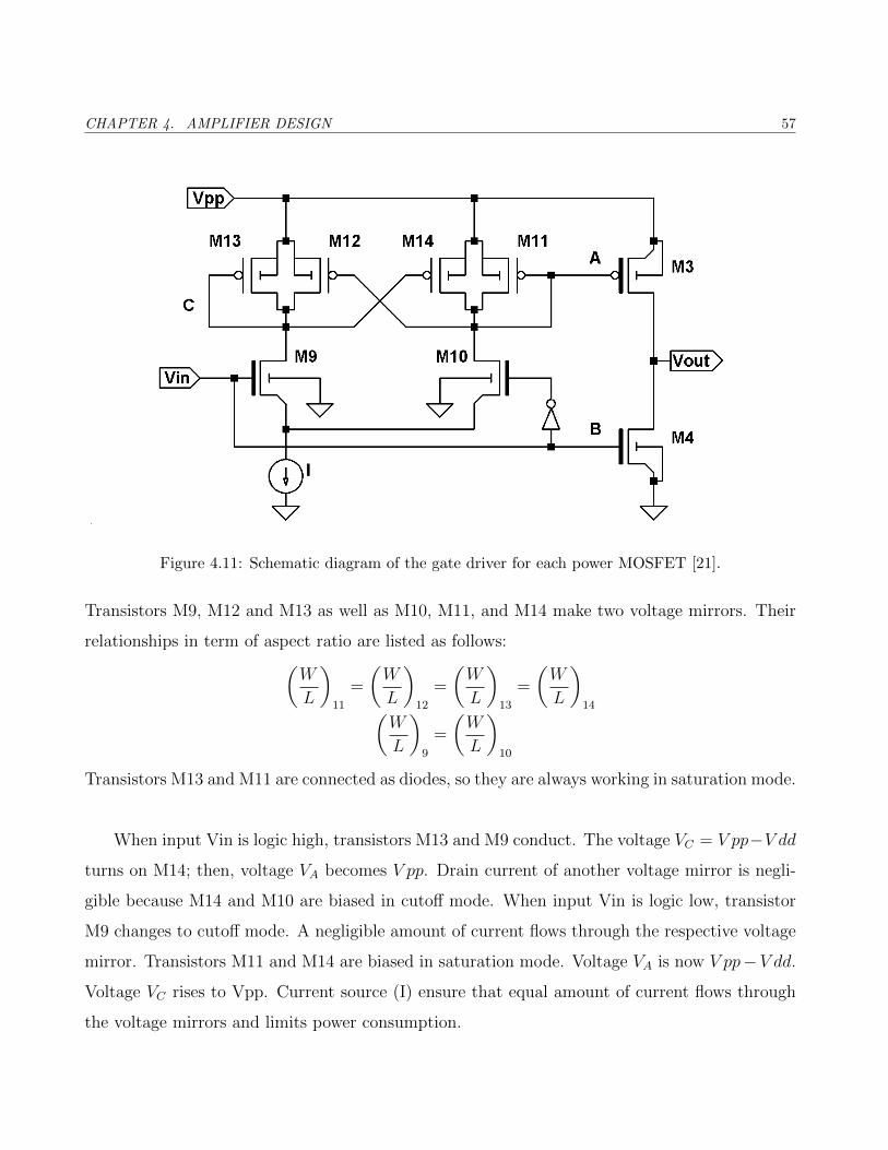
CHAPTER 4. AMPLIFIER DESIGN 57
Figure 4.11: Schematic diagram of the gate driver for each power MOSFET [21].
Transistors M9, M12 and M13 as well as M10, M11, and M14 make two voltage mirrors. Their
relationships in term of aspect ratio are listed as follows:(W
L
)11
=
(W
L
)12
=
(W
L
)13
=
(W
L
)14(
W
L
)9
=
(W
L
)10
Transistors M13 and M11 are connected as diodes, so they are always working in saturation mode.
When input Vin is logic high, transistors M13 and M9 conduct. The voltage VC = V pp−V dd
turns on M14; then, voltage VA becomes V pp. Drain current of another voltage mirror is negli-
gible because M14 and M10 are biased in cutoff mode. When input Vin is logic low, transistor
M9 changes to cutoff mode. A negligible amount of current flows through the respective voltage
mirror. Transistors M11 and M14 are biased in saturation mode. Voltage VA is now V pp− V dd.
Voltage VC rises to Vpp. Current source (I) ensure that equal amount of current flows through
the voltage mirrors and limits power consumption.

CHAPTER 4. AMPLIFIER DESIGN 58
4.3.1 Calculations
Estimation of M3 and M4
Transistors M3 and M4 control the rise time trise and fall time tfall of the gate signals of the
power transistors. Rise time is the duration that a voltage requires to increase from 10% to 90%
of its maximum level. Fall time is defined as the duration that a voltage needs to decrease from
90% to 10% of its maximum level. Based on given trise or tfall, the size of M3 and M4 can be
approximately estimated by differential equations [22] or a linear model t = 2.2 Rch Cgate. The
details of using the differential equation method for estimating the width of M4 can be found in
Appendix C. The estimated width of M3 and M4 were 215.3 µm and 197.2µm correspondingly.
After analysis of the simulation results, the width of WM3 and WM4 were aligned to 200 µm and
250 µm respectively.
Voltage Mirror
To determine the aspect ratio of M11 and M10, voltage VA, slew rate and equivalent capacitance
at node A are required. Transistors M11 and M10 are biased in saturation mode while conduct-
ing. Since IDM10= IDM11
, their aspect ratio can be determined by the expression below [21]:
K ′HVN
2
W10
L10(VGS − Vt HV N
)2 =K ′LV P
2
W11
L11[(V pp− VA)− Vt LV P
]2 (4.30)
where K ′HVN denotes the technological parameter for HV NMOS; Wn and Ln represent the width
and length of the respective transistors. Voltage Vin denotes the peak-to-peak amplitude of the input
signal, which equals V dd; VtLV P is the threshold voltage of LV PMOS, and V pp denotes the potential of
the high voltage supply. However, Equation (4.30) cannot apply to our situation directly, because the
mobility degradation correction is missing and a current mirror is attached at the end of the voltage
mirror. That alters the threshold voltage of M9 and M10. Expression (4.30) was modified to fit our
situation. We have,
K ′HVN
2
W10
L10
(VGS − VtHV N V BS)2
(1 + θHVN (VGS − Vt HV N V BS))
=K ′LV P
2
W11
L11
(V pp− VA)− Vt LV P]2
(1 + θLV P (VGS − Vt LV P))
(4.31)
where threshold voltage Vt HVN VBS is obtained through simulations. The subscripts HVN and LV P
represent high-voltage and low-voltage respectively. At node A, the relationship of current, slew rate
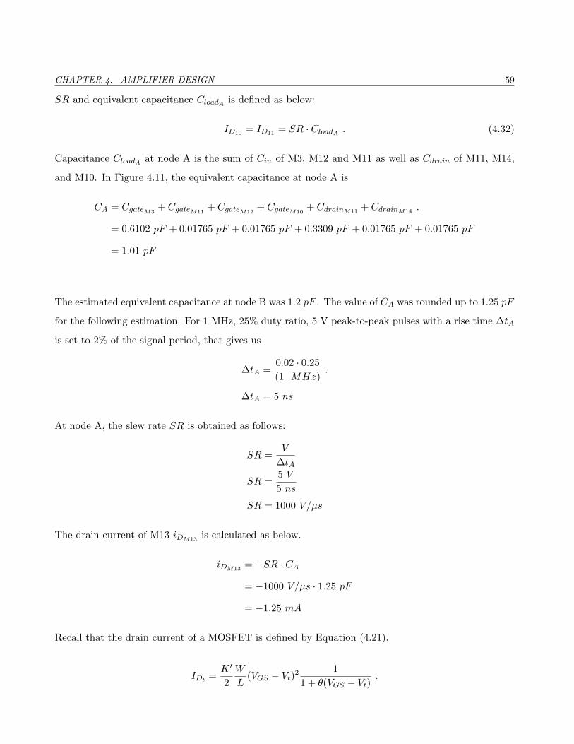
CHAPTER 4. AMPLIFIER DESIGN 59
SR and equivalent capacitance CloadA is defined as below:
ID10 = ID11 = SR · CloadA . (4.32)
Capacitance CloadA at node A is the sum of Cin of M3, M12 and M11 as well as Cdrain of M11, M14,
and M10. In Figure 4.11, the equivalent capacitance at node A is
CA = CgateM3+ CgateM11
+ CgateM12+ CgateM10
+ CdrainM11+ CdrainM14
.
= 0.6102 pF + 0.01765 pF + 0.01765 pF + 0.3309 pF + 0.01765 pF + 0.01765 pF
= 1.01 pF
The estimated equivalent capacitance at node B was 1.2 pF . The value of CA was rounded up to 1.25 pF
for the following estimation. For 1 MHz, 25% duty ratio, 5 V peak-to-peak pulses with a rise time ∆tA
is set to 2% of the signal period, that gives us
∆tA =0.02 · 0.25
(1 MHz).
∆tA = 5 ns
At node A, the slew rate SR is obtained as follows:
SR =V
∆tA
SR =5 V
5 ns
SR = 1000 V/µs
The drain current of M13 iDM13is calculated as below.
iDM13= −SR · CA
= −1000 V/µs · 1.25 pF
= −1.25 mA
Recall that the drain current of a MOSFET is defined by Equation (4.21).
IDt =K ′
2
W
L(VGS − Vt)2
1
1 + θ(VGS − Vt).
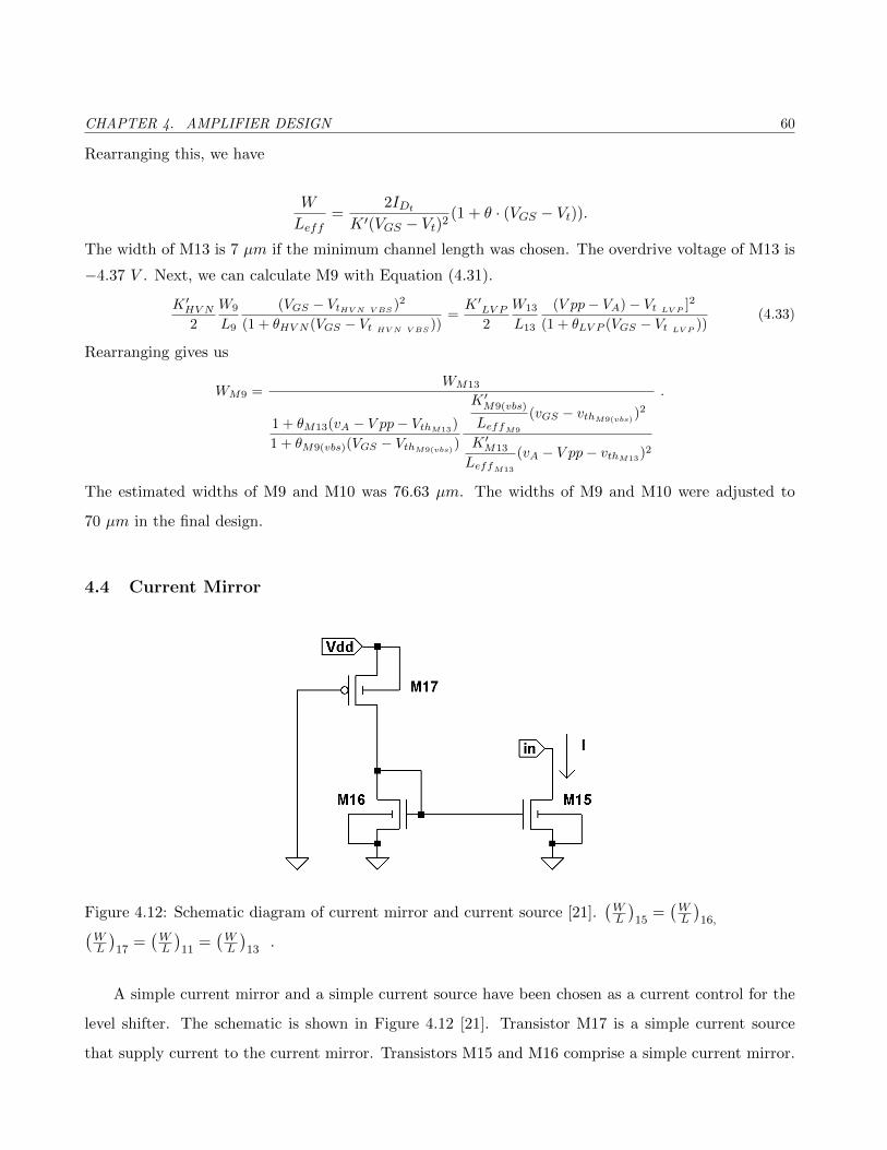
CHAPTER 4. AMPLIFIER DESIGN 60
Rearranging this, we have
W
Leff=
2IDtK ′(VGS − Vt)2
(1 + θ · (VGS − Vt)).
The width of M13 is 7 µm if the minimum channel length was chosen. The overdrive voltage of M13 is
−4.37 V . Next, we can calculate M9 with Equation (4.31).
K ′HVN
2
W9
L9
(VGS − VtHV N V BS)2
(1 + θHVN (VGS − Vt HV N V BS))
=K ′LV P
2
W13
L13
(V pp− VA)− Vt LV P]2
(1 + θLV P (VGS − Vt LV P))
(4.33)
Rearranging gives us
WM9 =WM13
1 + θM13(vA − V pp− VthM13)
1 + θM9(vbs)(VGS − VthM9(vbs))
K ′M9(vbs)
LeffM9
(vGS − vthM9(vbs))2
K ′M13
LeffM13
(vA − V pp− vthM13)2
.
The estimated widths of M9 and M10 was 76.63 µm. The widths of M9 and M10 were adjusted to
70 µm in the final design.
4.4 Current Mirror
Figure 4.12: Schematic diagram of current mirror and current source [21].(WL
)15
=(WL
)16,(
WL
)17
=(WL
)11
=(WL
)13
.
A simple current mirror and a simple current source have been chosen as a current control for the
level shifter. The schematic is shown in Figure 4.12 [21]. Transistor M17 is a simple current source
that supply current to the current mirror. Transistors M15 and M16 comprise a simple current mirror.
CHAPTER 4. AMPLIFIER DESIGN 61
Transistor M16 is always in active mode. It governs the current rate of the level shifter. However, the
current mirror has a low rejection to power supply variations.
Recall that (W
L
)15
=
(W
L
)16
. (4.34)
∴ vGS15 = vGS16 (4.35)
The drain current of M15 and M16 is
ID16 = ID15 =K ′LV P
2
W15
L15V ov215 (4.36)
where overdrive voltage V ov15 = VGS15 − VtLV P . We rearrange the previous equation to find the width
of M15:
W15 =2 ID L15
K ′LV P V ov152 (4.37)
An overdrive voltage of 0.45 V maintains M15 in saturation mode during operation. The estimated
widths of M15 and M16 were 235.7 µm. The widths of M15 and M16 were adjusted to 240 µm in the
final design.
Transistor M17 is a simple current source for the current mirror. The aspect ratio of M17 is
calculated with the equation below.
WM17
LeffM17
=−ID 2 (1 + θ (VGS − Vt))
K ′ (VGS − Vt)(4.38)
The estimated width of WM17 was 6.09 µm. It was adjusted to 7 µm after simulation.
In the long term, a more sophisticated current source that does not depend on supply voltage and
technological parameters should be used. For a simple current mirror, increasing the width of M15
reduces the minimum output voltage. Table 4.5 summarizes the final length and width of all transistors
used in power stage and gate drivers.
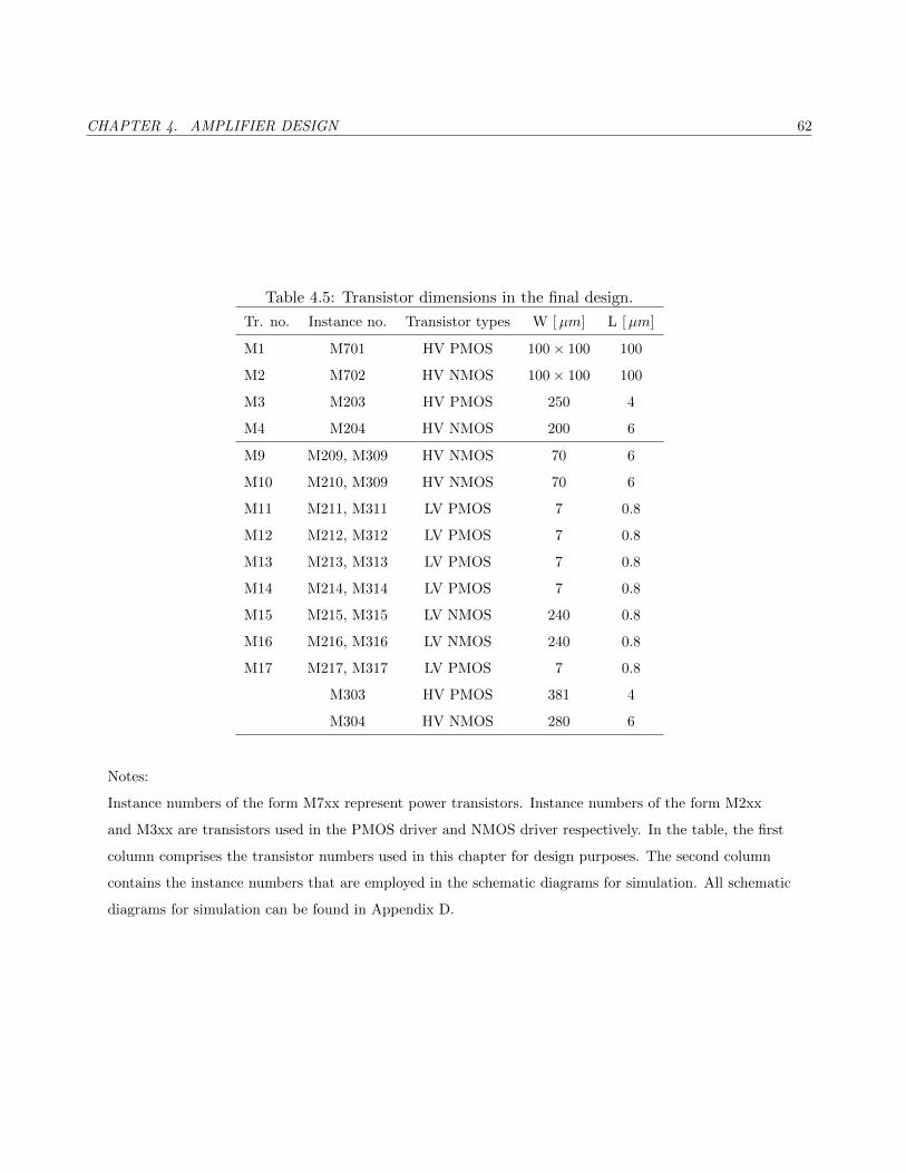
CHAPTER 4. AMPLIFIER DESIGN 62
Table 4.5: Transistor dimensions in the final design.
Tr. no. Instance no. Transistor types W [µm] L [µm]
M1 M701 HV PMOS 100× 100 100
M2 M702 HV NMOS 100× 100 100
M3 M203 HV PMOS 250 4
M4 M204 HV NMOS 200 6
M9 M209, M309 HV NMOS 70 6
M10 M210, M309 HV NMOS 70 6
M11 M211, M311 LV PMOS 7 0.8
M12 M212, M312 LV PMOS 7 0.8
M13 M213, M313 LV PMOS 7 0.8
M14 M214, M314 LV PMOS 7 0.8
M15 M215, M315 LV NMOS 240 0.8
M16 M216, M316 LV NMOS 240 0.8
M17 M217, M317 LV PMOS 7 0.8
M303 HV PMOS 381 4
M304 HV NMOS 280 6
Notes:
Instance numbers of the form M7xx represent power transistors. Instance numbers of the form M2xx
and M3xx are transistors used in the PMOS driver and NMOS driver respectively. In the table, the first
column comprises the transistor numbers used in this chapter for design purposes. The second column
contains the instance numbers that are employed in the schematic diagrams for simulation. All schematic
diagrams for simulation can be found in Appendix D.
CHAPTER 4. AMPLIFIER DESIGN 63
4.5 Digital Block
A digital block is implemented with combinational logic to provide the functions of power stage
enabling, faulty signal filtering and output buffering. It is located prior to the gate drivers of the
amplifier. The schematic of the digital block is shown in Figure 4.13. It accepts a standard 5 V power
supply, consisting of three inputs and two outputs. Three inputs are enable, PMOS signal and NMOS
signal; denoted by the variables EN, inP and inN . Two outputs are NMOS signal output and PMOS
signal output; designated by YN and YP . Outputs of the digital block are routed to the input of the
level shifters. Each level shifter requires these signals and their complements for driving its transistors.
Therefore, multiple stages of inverter are required to handle large capacitor loads. Dalsa’s CMOS cell
library manual [23] provides parameters and formula for calculating the propagation delay time of each
stage.
Tp[ns] = Tintrinsic [ns] + Tdrive [ns/pF ]× Cload [pF ] (4.39)
where Tp denotes the propagation delay time of the respective stage; Tintrinsic and Tdrive are parameters
provided in Dalsa’s CMOS cell library manual. The total propagation delay time of multiple stages is
acquired by summing the delay time of each stage.
Enable pin is responsible for the on-off function of the power stage. When EN input is low, the cir-
cuitry locks up the power stage regardless of the inputs. This is done by biasing both power transistors
in the cut off mode. When EN is high, outputs will follow the respective inputs, except when a faulty
state inP , inN = 0,1 is identified. This state will turns both power transistors on together and
cause permanent damage to them. The combinational logic was implemented with the digital library
offered in the design kit. Table 4.6 is the truth table of the digital block.
On the left hand side of the truth table, under the input variables, are eight rows of all possible
combinations of 1’s and 0’s that these variables may have. The first four rows (enable EN = 0) indicate
that the amplifier is working in standby mode. Therefore, output variable YP and YN assign logic high
and logic low respectively for biasing power transistors in the cut off mode. For rows five, seven and
eight, outputs follow the respective inputs. The input of the sixth row overrides, because it eventually
creates a short by turning on both power transistors.
The simplified Boolean function for the two outputs YP and YN can be derived by solving the Kar-

CHAPTER 4. AMPLIFIER DESIGN 64
Table 4.6: Truth Table.
EN inP inN YP (1) YN (1) PMOS NMOS
0 0 0 1 0 off off
0 0 1 1 0 off off
0 1 0 1 0 off off
0 1 1 1 0 off off
1 0 0 0 0 on off
(2) 1 0 1 1 0 off off
1 1 0 1 0 off off
1 1 1 1 1 off on
Note 1:
YP is active low and YN is active high.
Note 2:
The state inP = 0 and inN = 1 will turn on both power transistors; therefore,
combinational circuit switches them off for protection.
Figure 4.13: Schematic diagram of the digital block.

CHAPTER 4. AMPLIFIER DESIGN 65
naugh Maps shown in Figure 4.14(a) and (b). The corresponding simplified sum of product expressions
are listed directly below each map.
Figure 4.14: Map for input functions and output of the digital block. (a) Functions of PMOS (b)
Functions of NMOS.
Chapter 5
Simulation Results
5.1 Pre-layout simulations
The performance of the proposed integrated amplifier has been appraised with various configurations
in order to establish a comprehensive solution that demonstrates an acceptable level of third harmonic
and efficiency. Figure 5.1 and Figure 5.2 show the output voltage vDSM702and the power transistors’
drain current IDM701and IDM702
waveforms in time domain at steady state. Since the output stage is di-
rectly connected to an ultrasound transducer instead of through a tuned network, the class DE amplifier
does not operate at its optimum working condition. This can be identified when a small trough appears
at the rising or falling edge of the vDSM702waveforms in Figure 5.1. Figure 5.3 illustrates the Discrete
Fourier Transform DFT of the output voltage waveform at steady state. Spectrum was obtained using
the DFT function of Calculator in the Cadence’s Analog Design Environment. The simulation was run
for 100 µs; one hundred periods were generated. The time period for DFT was taken from 50µs to 100µs.
Figure 5.4 plots the ratio of third harmonic to fundamental for the voltage waveform, as a function
of duty ratio with a varying values of external capacitance at steady state. The vertical axis of the
Figure is the percentage of magnitude of 3rd harmonic to the magnitude of the fundamental. The
horizontal axis represents the duty ratio D of the control signals. In other words, duty ratio D excludes
delays imposed by the combinational circuit, gate drivers and power transistors. Therefore, the turn-on
duration measured at the output is longer than the turn-on duration measured at the input. An input
pulse with 0.19 duty ratio eventually creates an output pulse with a duty ratio of 0.25. From the figure,
the third harmonic becomes lowest when the duty ratio D was between 0.22 and 0.23 at steady state.
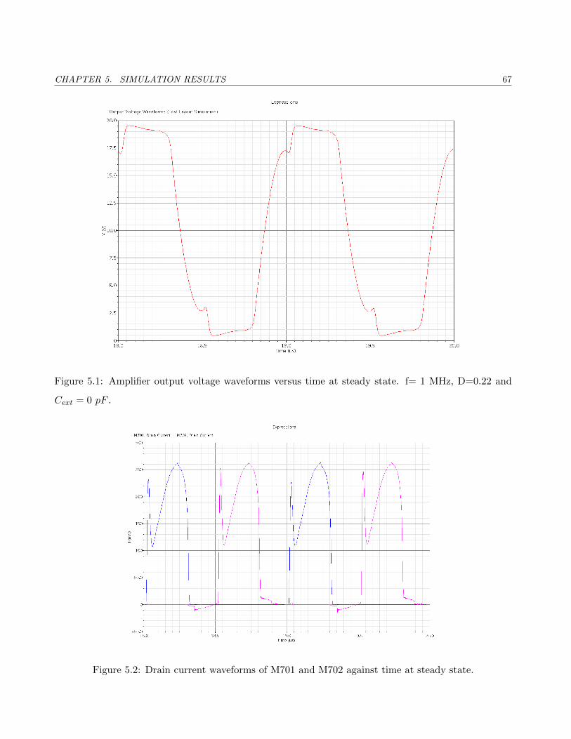
CHAPTER 5. SIMULATION RESULTS 67
Figure 5.1: Amplifier output voltage waveforms versus time at steady state. f= 1 MHz, D=0.22 and
Cext = 0 pF .
Figure 5.2: Drain current waveforms of M701 and M702 against time at steady state.

CHAPTER 5. SIMULATION RESULTS 68
Figure 5.3: Discrete Fourier Transform of the amplifier’s output voltage waveforms at steady state.
The third harmonic is approximately 18% of the fundamental without any external capacitance and it
is below 5% with an external capacitance of 1 nF. High current spikes are generated when the ampli-
fier starts. Increasing the external capacitance will increase the magnitude of current spikes and the
width of the power supply lines; therefore, the maximum capacitance of the external capacitor is limited
to 1 nF. In addition, an external capacitance of more than 1 nF will bring the efficiency down below 80 %.
Figure 5.5 plots the steady state efficiency versus switch-on duty ratio D for a varying external
capacitance. As the external capacitance increases, the driver efficiency decreases and the gaps between
curves become wider. Depending on the external capacitance, the point of maximum efficiency occurs
in between D = 0.24 and D = 0.27. In general, the efficiency of the proposed design is above 80%
within the configurations that have been tested. The amplifier efficiency is higher without the external
capacitance because the switching loss is lower.
Figure 5.6 illustrates an overview of amplifier’s output power to Rs1 against switch-on duty ratio
D for a varying value of external capacitance. Output power is defined as the power consumption
of the resistor Rs1, the series resistor in the fundamental branch in the ultrasound transducer model,
which represents the energy delivery to the acoustic power field, plus mechanical losses at fundamental
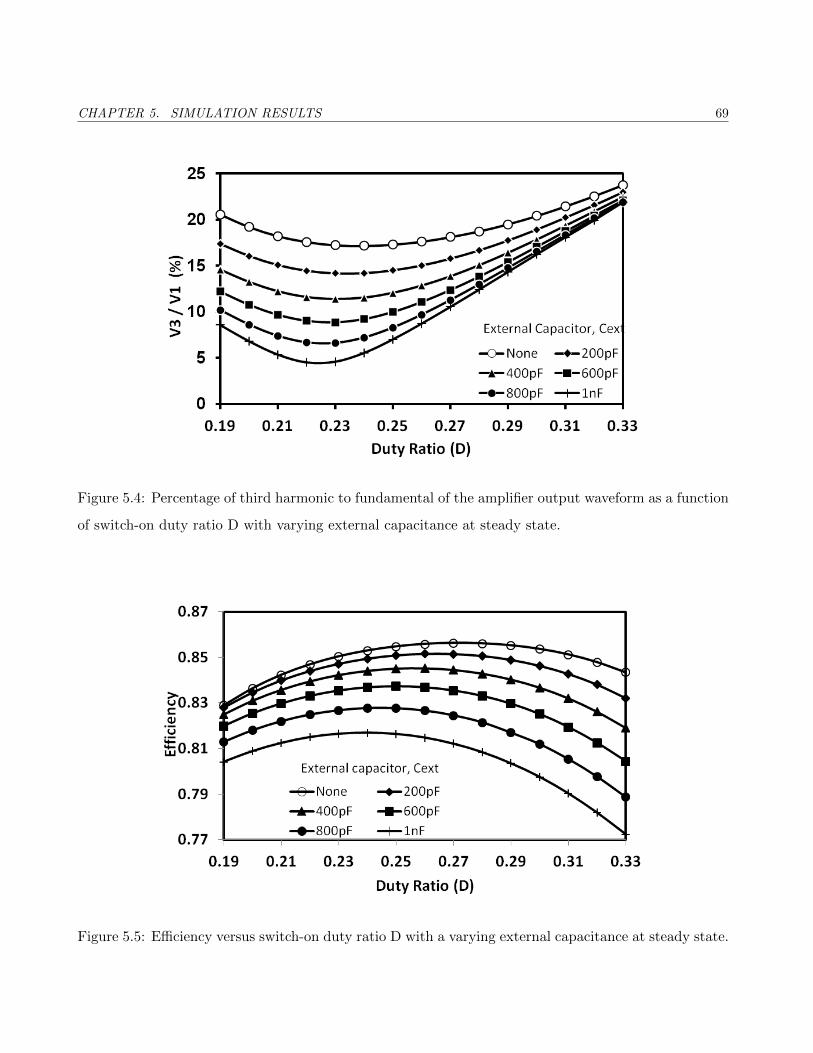
CHAPTER 5. SIMULATION RESULTS 69
Figure 5.4: Percentage of third harmonic to fundamental of the amplifier output waveform as a function
of switch-on duty ratio D with varying external capacitance at steady state.
Figure 5.5: Efficiency versus switch-on duty ratio D with a varying external capacitance at steady state.
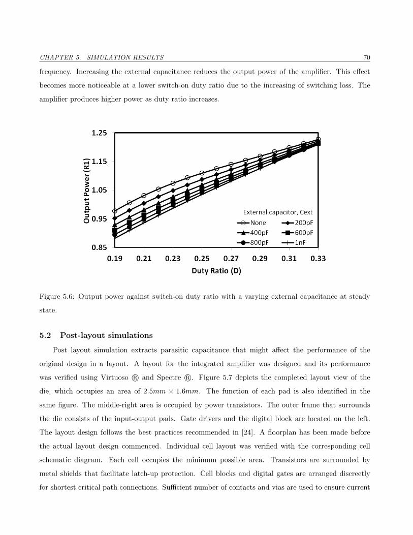
CHAPTER 5. SIMULATION RESULTS 70
frequency. Increasing the external capacitance reduces the output power of the amplifier. This effect
becomes more noticeable at a lower switch-on duty ratio due to the increasing of switching loss. The
amplifier produces higher power as duty ratio increases.
Figure 5.6: Output power against switch-on duty ratio with a varying external capacitance at steady
state.
5.2 Post-layout simulations
Post layout simulation extracts parasitic capacitance that might affect the performance of the
original design in a layout. A layout for the integrated amplifier was designed and its performance
was verified using Virtuoso R© and Spectre R©. Figure 5.7 depicts the completed layout view of the
die, which occupies an area of 2.5mm × 1.6mm. The function of each pad is also identified in the
same figure. The middle-right area is occupied by power transistors. The outer frame that surrounds
the die consists of the input-output pads. Gate drivers and the digital block are located on the left.
The layout design follows the best practices recommended in [24]. A floorplan has been made before
the actual layout design commenced. Individual cell layout was verified with the corresponding cell
schematic diagram. Each cell occupies the minimum possible area. Transistors are surrounded by
metal shields that facilitate latch-up protection. Cell blocks and digital gates are arranged discreetly
for shortest critical path connections. Sufficient number of contacts and vias are used to ensure current
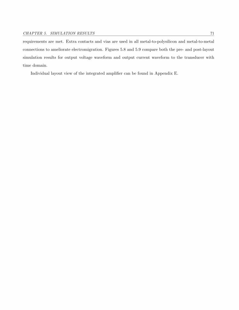
CHAPTER 5. SIMULATION RESULTS 71
requirements are met. Extra contacts and vias are used in all metal-to-polysilicon and metal-to-metal
connections to ameliorate electromigration. Figures 5.8 and 5.9 compare both the pre- and post-layout
simulation results for output voltage waveform and output current waveform to the transducer with
time domain.
Individual layout view of the integrated amplifier can be found in Appendix E.


CHAPTER 5. SIMULATION RESULTS 73
Figure 5.8: Output voltage waveforms of pre- and post-layout simulations.
Figure 5.9: Output current waveforms of pre- and post-layout simulations.
Chapter 6
Conclusions
The objective of this thesis was to design a CMOS power amplifier for a piezoelectric transducer to
be installed near the piezoelectric resonator inside an MRI environment. Several of the challenges of
designing the integrated amplifier have been addressed:
1. Each amplifier should occupy a minimum possible area: an effort was made to reduce the chip
area by avoiding the use of on-chip resistors, inductors and capacitors. Also, transistors were
designed to be as small as possible. The overall area of the amplifier is 2.5 mm by 1.6 mm, which
is smaller than any other design reported in the literature, such as [13]. Without the pads, the
amplifier occupies an area of 0.9 mm2.
2. The use of magnetic components, such as inductors, has been avoided because they can interfere
with the MRIs reception and distort the image [3].
3. The amplifier is efficient: overall efficiency is 80%. This, combined with the low chip area, will
enable the integration of several amplifiers in a single chip.
4. The proposed amplifier is capable of delivering 1 W of power to the load at 1 MHz. The third
harmonic level is below 20% on the electrical side in the worst case. The third harmonic can
be reduced at the cost of some efficiency by increasing the value of the external capacitor. The
expected third harmonic level in the acoustic pressure field should be approximately 9.5 dB below
the electrical level according to the measurements reported in Chapter 3. Figure 6.1 illustrates
the projected percentage of the acoustic third harmonic to fundamental as a function of switch-
on duty ratio D, with a varying external capacitance based on the results of circuit simulations,
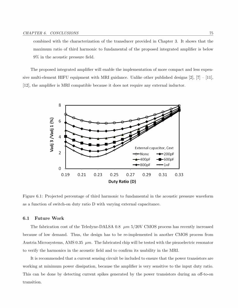
CHAPTER 6. CONCLUSIONS 75
combined with the characterization of the transducer provided in Chapter 3. It shows that the
maximum ratio of third harmonic to fundamental of the proposed integrated amplifier is below
9% in the acoustic pressure field.
The proposed integrated amplifier will enable the implementation of more compact and less expen-
sive multi-element HIFU equipment with MRI guidance. Unlike other published designs [2], [7] – [11],
[12], the amplifier is MRI compatible because it does not require any external inductor.
Figure 6.1: Projected percentage of third harmonic to fundamental in the acoustic pressure waveform
as a function of switch-on duty ratio D with varying external capacitance.
6.1 Future Work
The fabrication cost of the Teledyne-DALSA 0.8 µm 5/20V CMOS process has recently increased
because of low demand. Thus, the design has to be re-implemented in another CMOS process from
Austria Microsystems, AMS 0.35 µm. The fabricated chip will be tested with the piezoelectric resonator
to verify the harmonics in the acoustic field and to confirm its usability in the MRI.
It is recommended that a current sensing circuit be included to ensure that the power transistors are
working at minimum power dissipation, because the amplifier is very sensitive to the input duty ratio.
This can be done by detecting current spikes generated by the power transistors during an off-to-on
transition.
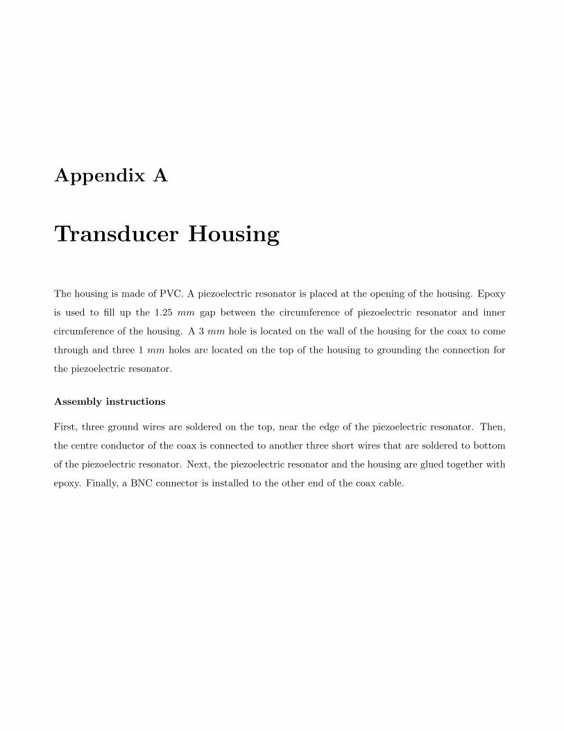
Appendix A
Transducer Housing
The housing is made of PVC. A piezoelectric resonator is placed at the opening of the housing. Epoxy
is used to fill up the 1.25 mm gap between the circumference of piezoelectric resonator and inner
circumference of the housing. A 3 mm hole is located on the wall of the housing for the coax to come
through and three 1 mm holes are located on the top of the housing to grounding the connection for
the piezoelectric resonator.
Assembly instructions
First, three ground wires are soldered on the top, near the edge of the piezoelectric resonator. Then,
the centre conductor of the coax is connected to another three short wires that are soldered to bottom
of the piezoelectric resonator. Next, the piezoelectric resonator and the housing are glued together with
epoxy. Finally, a BNC connector is installed to the other end of the coax cable.

Figure A.1: Transducer Housing
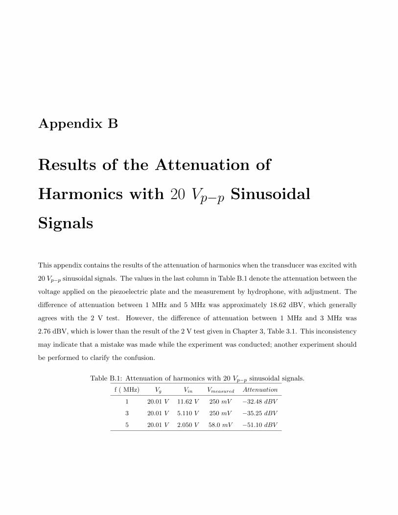
Appendix B
Results of the Attenuation of
Harmonics with 20 Vp−p Sinusoidal
Signals
This appendix contains the results of the attenuation of harmonics when the transducer was excited with
20 Vp−p sinusoidal signals. The values in the last column in Table B.1 denote the attenuation between the
voltage applied on the piezoelectric plate and the measurement by hydrophone, with adjustment. The
difference of attenuation between 1 MHz and 5 MHz was approximately 18.62 dBV, which generally
agrees with the 2 V test. However, the difference of attenuation between 1 MHz and 3 MHz was
2.76 dBV, which is lower than the result of the 2 V test given in Chapter 3, Table 3.1. This inconsistency
may indicate that a mistake was made while the experiment was conducted; another experiment should
be performed to clarify the confusion.
Table B.1: Attenuation of harmonics with 20 Vp−p sinusoidal signals.
f ( MHz) Vg Vin Vmeasured Attenuation
1 20.01 V 11.62 V 250 mV −32.48 dBV
3 20.01 V 5.110 V 250 mV −35.25 dBV
5 20.01 V 2.050 V 58.0 mV −51.10 dBV

Appendix C
An Estimation of M4’s width using the
Differential Equation Method
Suppose that the output of the gate driver is connected to a capacitive load C that is equivalent to the
gate capacitor of M1. The gate width of the transistor can be estimated by the differential equation
method [22]. When C has been fully charged to supply voltage V pp for a while, M4 is turned on. It
soon enters into saturation mode. The rate of change of the capacitor voltage is defined as follows:
CdV
dt= −iDM4
.
Substituting the saturation current expression for iDM4[22], we get
−C dV
dt=K ′
2
W
L(VGS − Vt)2
1
1 + θ(VGS − Vt),
Integrating both sides,
−C∫ Vov
V 90%dV =
∫ τ
0dtK ′
2
W
L(VGS − Vt)2
1
1 + θ(VGS − Vt), (C.1)
where τ represents the moment that M4 transfers from saturation mode to triode mode; Vov stands for
overdrive voltage or (VGS −Vt) for M4, and V 90% is 90% of V pp. Evaluating the the first integral gives
us ∫ Vov
V 90%dV = V ov − 0.9 V pp = Vsat
The second integral is given by: ∫ τ
0dt = τ .
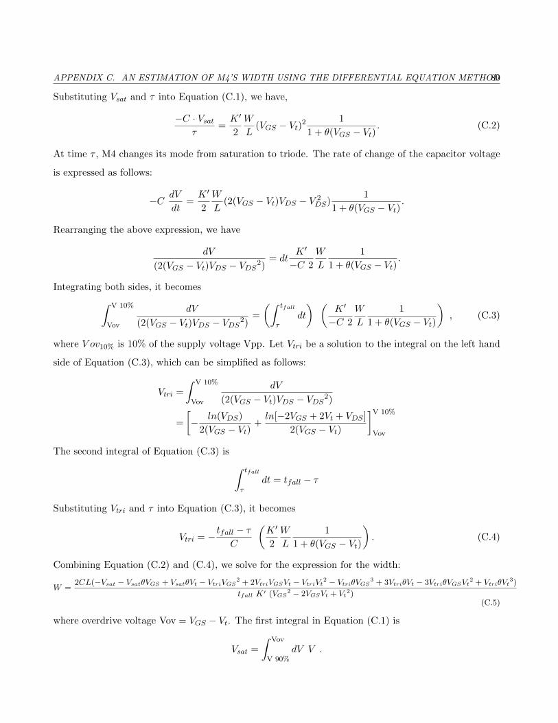
APPENDIX C. AN ESTIMATION OF M4’S WIDTH USING THE DIFFERENTIAL EQUATION METHOD80
Substituting Vsat and τ into Equation (C.1), we have,
−C · Vsatτ
=K ′
2
W
L(VGS − Vt)2
1
1 + θ(VGS − Vt). (C.2)
At time τ , M4 changes its mode from saturation to triode. The rate of change of the capacitor voltage
is expressed as follows:
−C dV
dt=K ′
2
W
L(2(VGS − Vt)VDS − V 2
DS)1
1 + θ(VGS − Vt).
Rearranging the above expression, we have
dV
(2(VGS − Vt)VDS − VDS2)= dt
K ′
−C 2
W
L
1
1 + θ(VGS − Vt).
Integrating both sides, it becomes∫ V 10%
Vov
dV
(2(VGS − Vt)VDS − VDS2)=
(∫ tfall
τdt
) (K ′
−C 2
W
L
1
1 + θ(VGS − Vt)
), (C.3)
where V ov10% is 10% of the supply voltage Vpp. Let Vtri be a solution to the integral on the left hand
side of Equation (C.3), which can be simplified as follows:
Vtri =
∫ V 10%
Vov
dV
(2(VGS − Vt)VDS − VDS2)
=
[− ln(VDS)
2(VGS − Vt)+ln[−2VGS + 2Vt + VDS ]
2(VGS − Vt)
]V 10%
Vov
The second integral of Equation (C.3) is ∫ tfall
τdt = tfall − τ
Substituting Vtri and τ into Equation (C.3), it becomes
Vtri = −tfall − τ
C
(K ′
2
W
L
1
1 + θ(VGS − Vt)
). (C.4)
Combining Equation (C.2) and (C.4), we solve for the expression for the width:
W =2CL(−Vsat − VsatθVGS + VsatθVt − VtriVGS
2 + 2VtriVGSVt − VtriVt2 − VtriθVGS
3 + 3VtriθVt − 3VtriθVGSVt2 + VtriθVt
3)
tfall K′ (VGS2 − 2VGSVt + Vt
2)(C.5)
where overdrive voltage Vov = VGS − Vt. The first integral in Equation (C.1) is
Vsat =
∫ Vov
V 90%dV V .

APPENDIX C. AN ESTIMATION OF M4’S WIDTH USING THE DIFFERENTIAL EQUATION METHOD81
The first integral in Equation (C.3) is evaluated as follows.
Vtri =
∫ V 10%
Vov
dV
(2(VGS − Vt)VDS − VDS2)V −2
Applying Equation (C.5), the width of M4 is calculated as follows:
WM4 =2CL(−Vsat − VsatθVGS + VsatθVt − Vtri(VGS)2 + 2VtriVGSVt − VtriVt2 − Vtriθ(VGS)3 + · · ·
tfall K ′ (VGS2 − 2VGSVt + Vt
2).
The estimated width of M4 was 197.2 µm.
Appendix D
Schematic Diagram
Schematic diagrams used in Spectre R© for simulations.
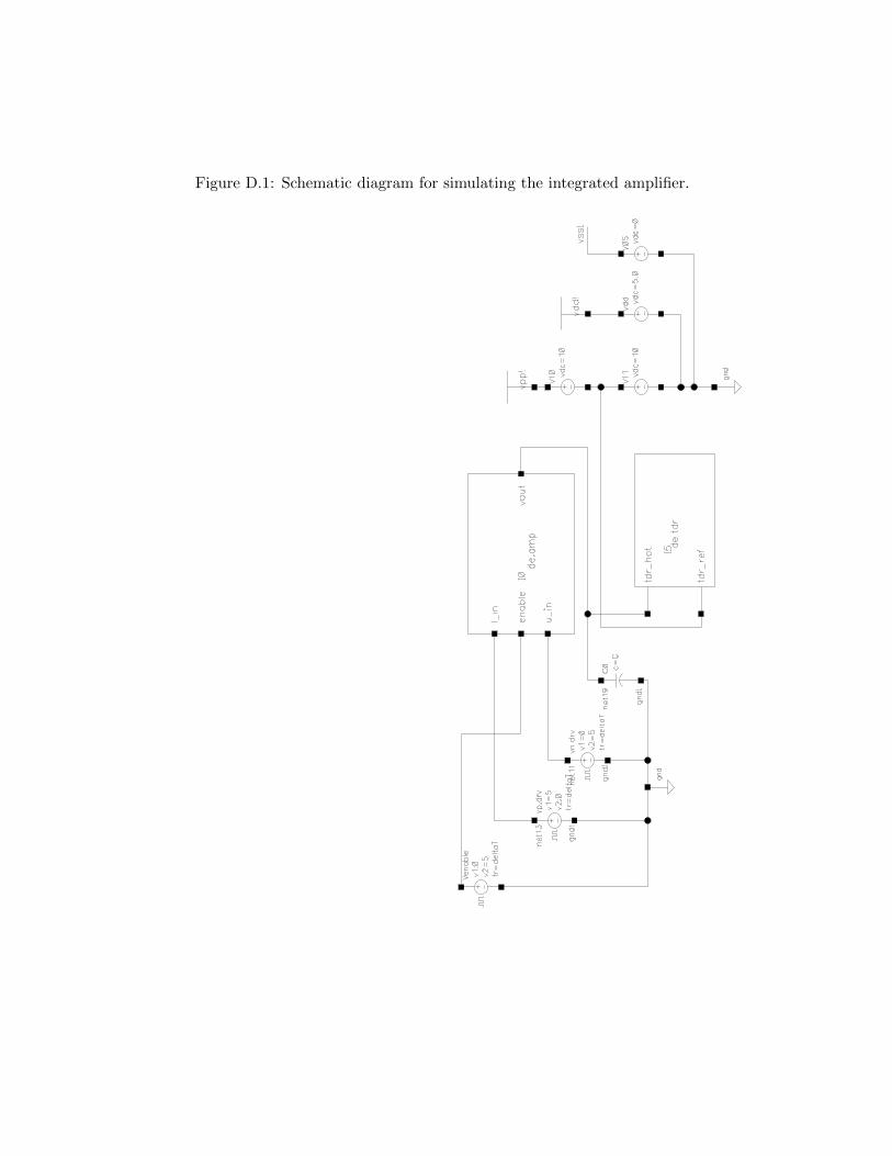
Figure D.1: Schematic diagram for simulating the integrated amplifier.
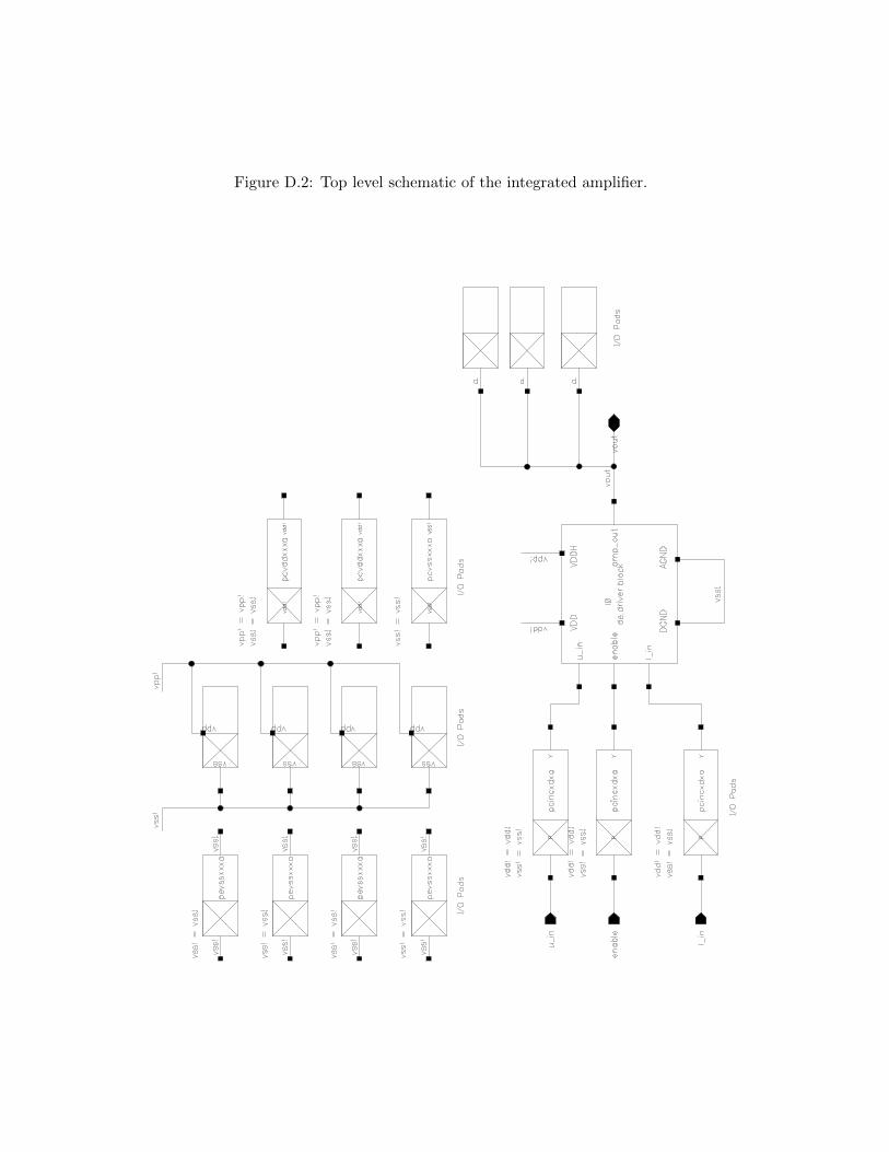
Figure D.2: Top level schematic of the integrated amplifier.
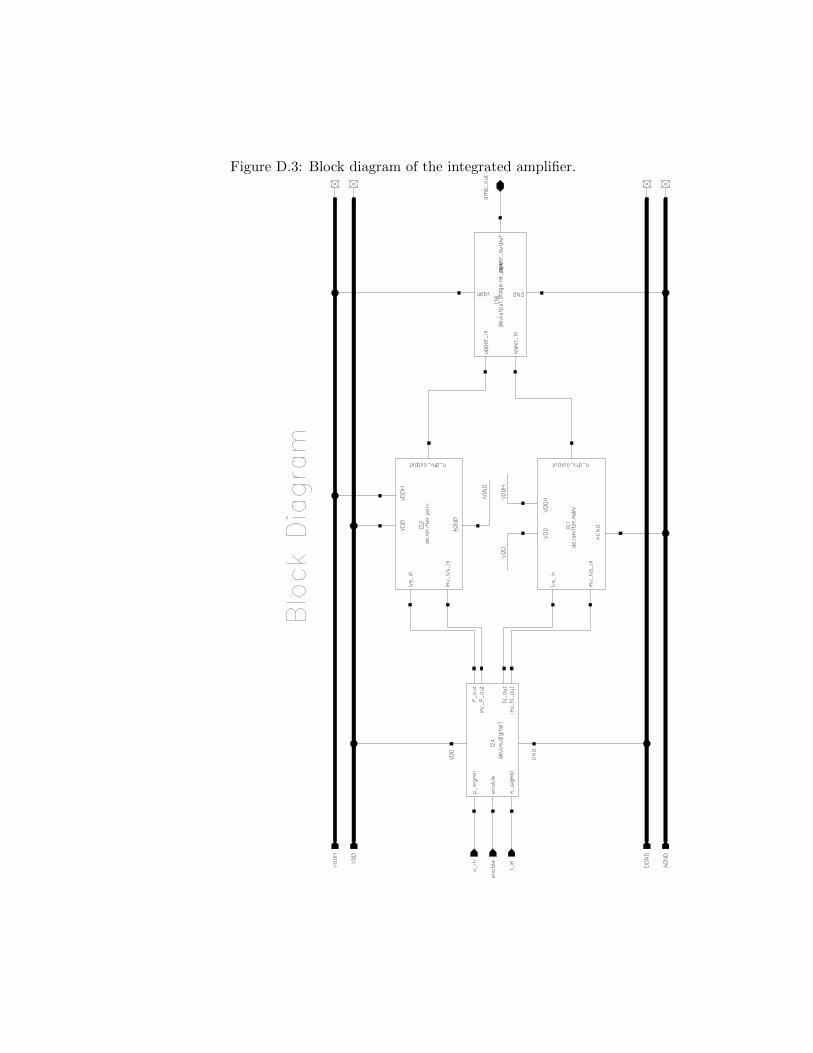
Figure D.3: Block diagram of the integrated amplifier.
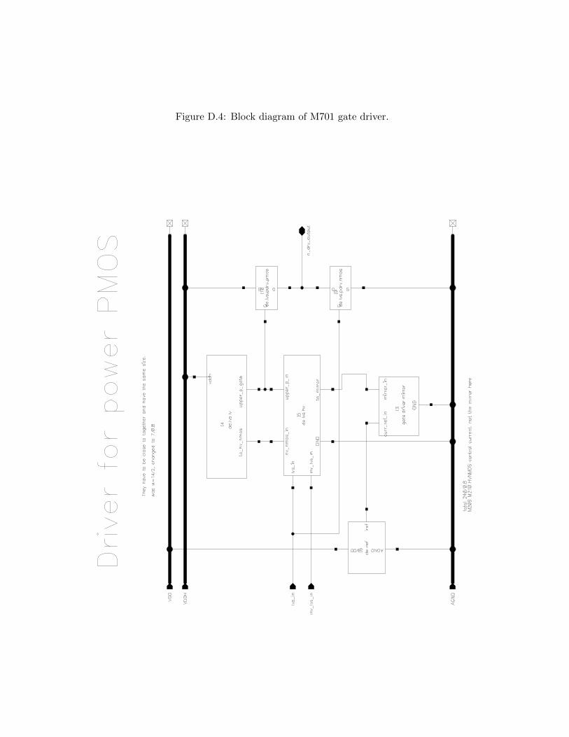
Figure D.4: Block diagram of M701 gate driver.
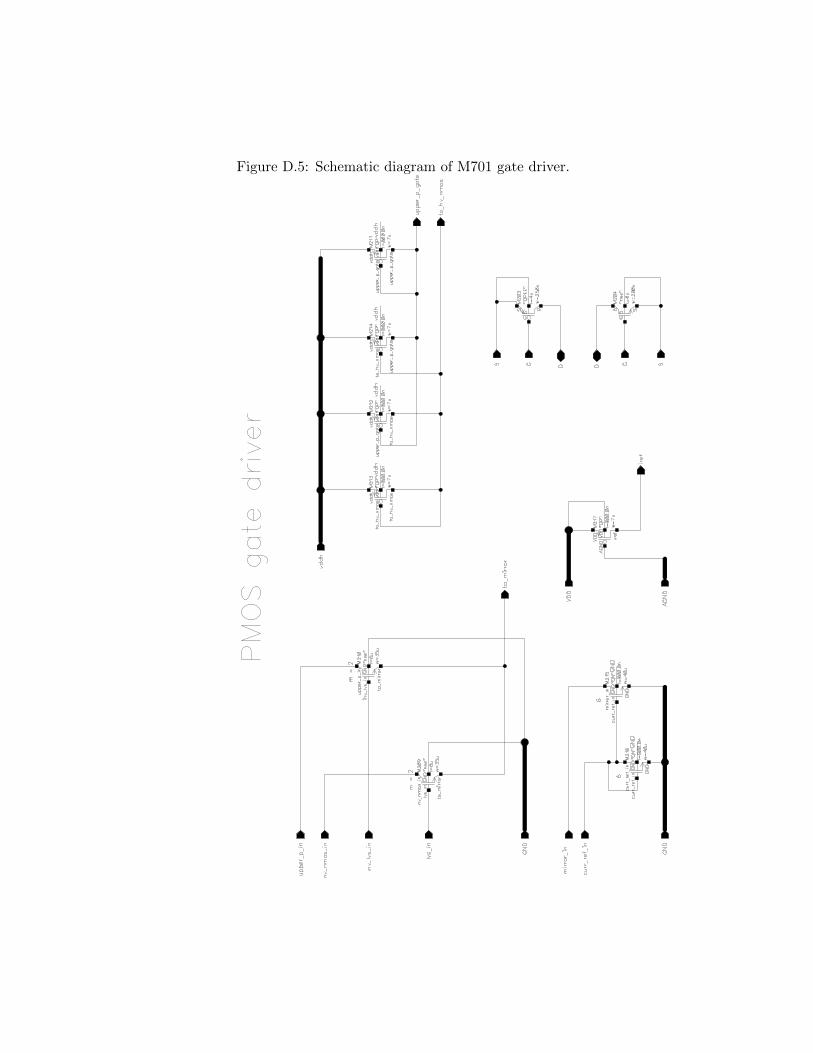
Figure D.5: Schematic diagram of M701 gate driver.
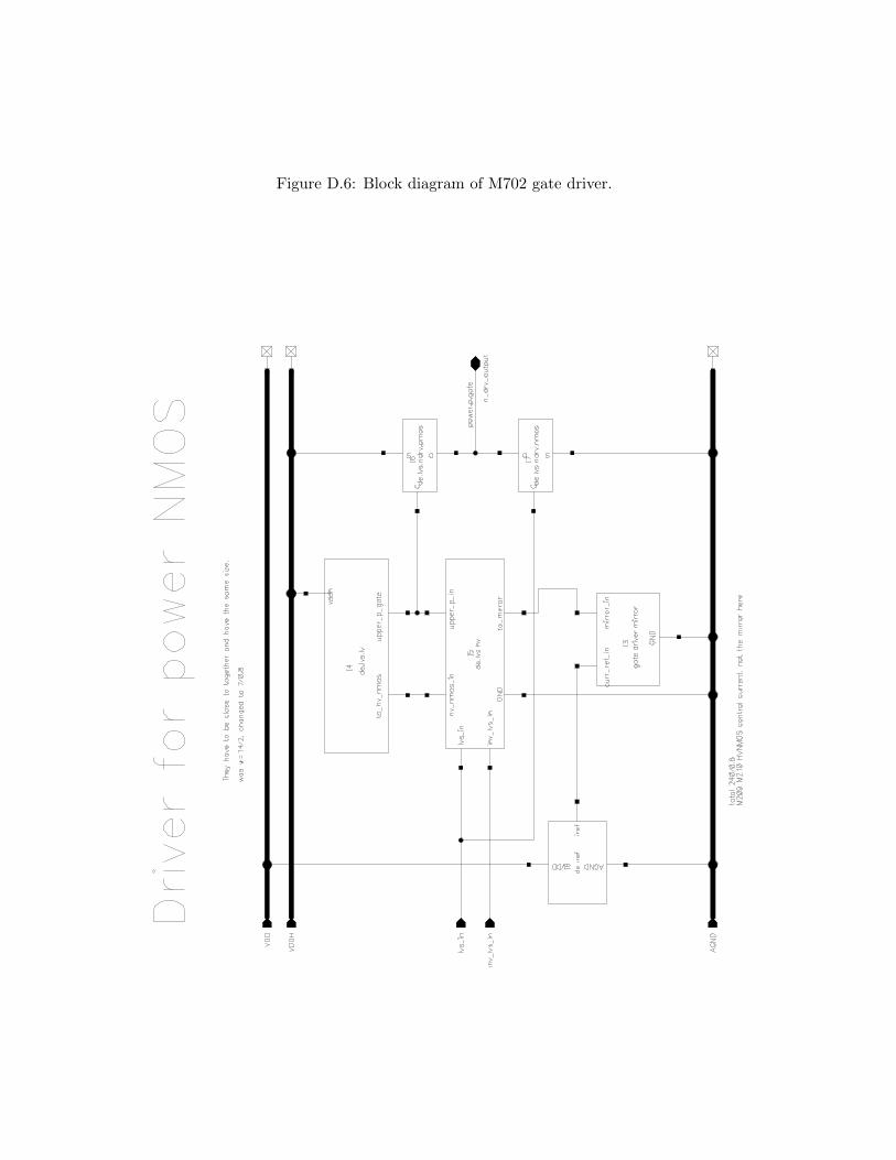
Figure D.6: Block diagram of M702 gate driver.
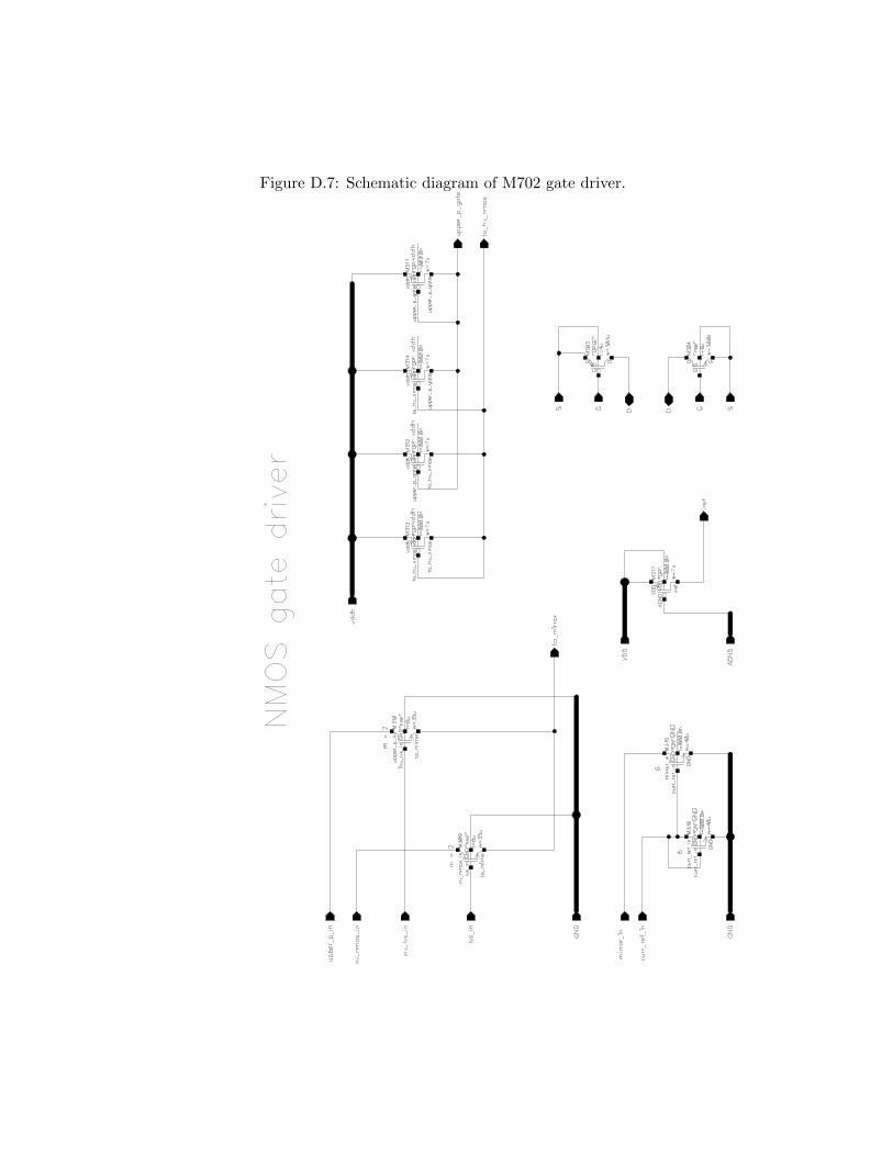
Figure D.7: Schematic diagram of M702 gate driver.
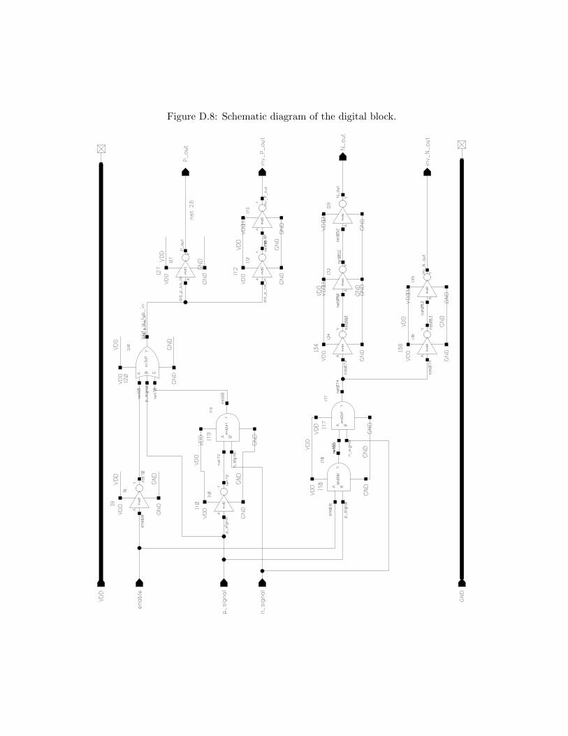
Figure D.8: Schematic diagram of the digital block.
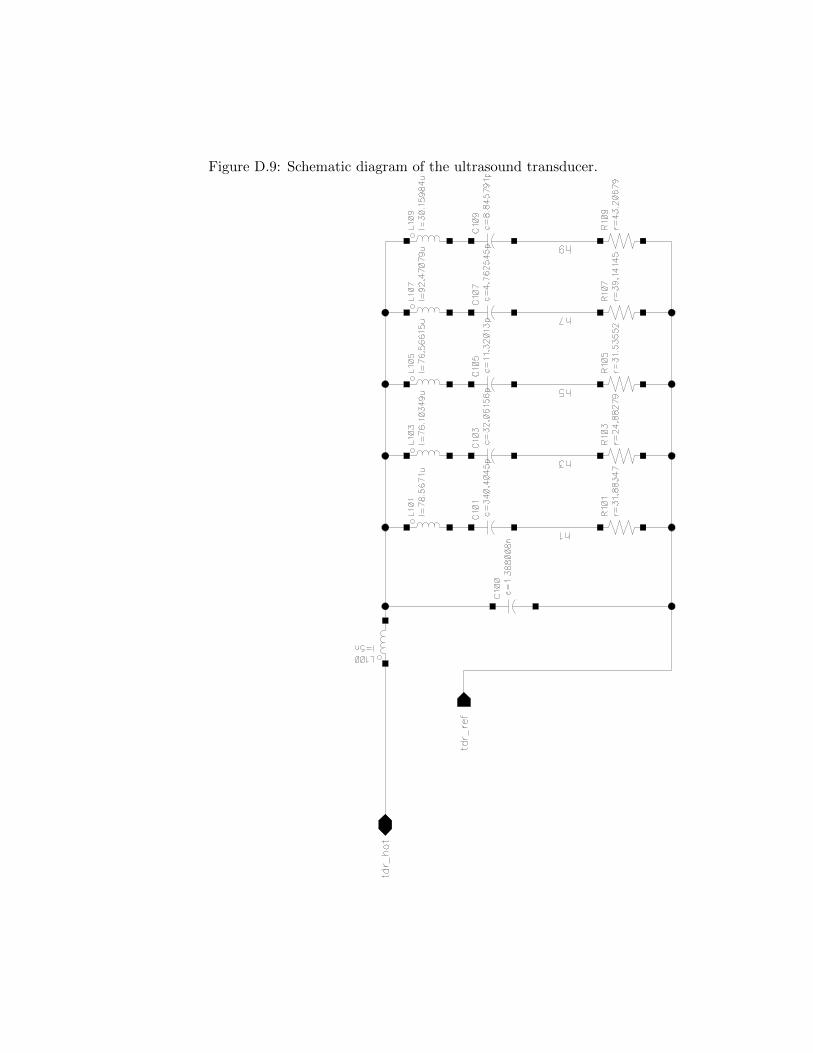
Figure D.9: Schematic diagram of the ultrasound transducer.
Appendix E
Layout View
The layout views used in Virtuoso for simulations.
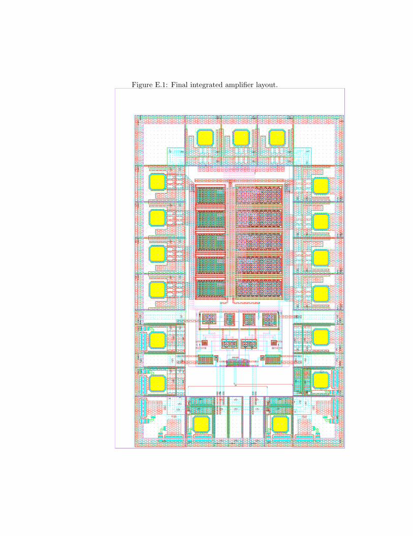
111
111
111
111
111
111
111
111
1111
1111
1111
1111
1111
1111
1111
1111
111
111
111
111
111
111
111
111
111
111
111
111
11
11
11
11 11
1111
11
1
11
11
11
1111
11
11
11
11
11
11
11
1111111111111111
11111111111111
111
111
11111
1111
1111
1111
1111
11
1111
1111
1111
1111
1111
1111
1111
1111
1111
1111
1111
1111
111 11 11
11111111 11111111
1111
1111
1111
1111
1111
1111
1111
111111 111111
1111
1111
1111
1111
1111
1111
111
111
111
111
111
111
1111
1111
1111
1111
1111
1111
11111111
1111111111
1111111111
11111111
111111111111
11111111
1111 111 11 11 11111
111
111
111
111
111
111
111
111
111
111
111
111
111
111
111
111
111
111
111
111
111
111
111
111
111
111
111
111
111
111
111
111
111
111
111
111
111
111
111
111
111
111
111
111
111
111111111111 1 1111
11 111
1111
1111
11111
11 111
111
1111
1111
1111
1111
11111
11 111
111
1111
1111
11111
11 111
111 1
1111
111 11
11 111
111
111
1111 111
1111
1111
11111
11 111
111
1111
1111
1111
1111
11111
11 111
111
1111
1111
11111
11 111
111 1
1111
111 11
11 111
111
111
1111 1 11 111 1 111
111
111
11
111
111
11111
1111
111
11 111
111
111 11
111
111
1111
111
11111
1111
1111
111 1 1
1111
111
111
111
111
111
111
111
111
111
11
111
111
11111
1111
111
11 111
111
111 11
111
111
1111
111
11111
1111
1111
111 1 1
1111
111
111
111
111
111
111
11
1111 111
1111
1111
11111
11 111
111
1111
1111
1111
1111
11111
11 111
111
1111
1111
11111
11 111
111 1
1111
111 11
11 111
111
111
1111 111
1111
1111
11111
11 111
111
1111
1111
1111
1111
11111
11 111
111
1111
1111
11111
11 111
111 1
1111
111 11
11 111
111
111
111111111111 1 11
1111
111
11
111
111
11111
1111
111
11 111
111
111 11
111
111
1111
111
11111
1111
1111
111 1 1
1111
111
111
111
111
111
111
111
111
111
11
111
111
11111
1111
111
11 111
111
111 11
111
111
1111
111
11111
1111
1111
111 1 1
1111
111
111
111
111
111
111
11
222
2222
2222
222
222
222 222 222
222
222
222
222
222
222
222
22
22
22
22
22
22
22
22
22
22
22
22
222
22222222
222
2222
2222
22222222 222222
2222
2222222 22222 222222222
222
222
222
222
222
222
222
222
222
222
2222
22
22
222
222222
222222
222222
222222
222222
222222
222222
222222
2222 222
222
222
222
222 22
22
22
22
22
222
222
222
222
222
222
222
222
22
22
22
22
22
222222
222222
222222
222222
222222
222222
222222
222222
2222 222
222
222
222
222 22
22
22
22
22
222
222
222
222
222
222
222
22
22
22222222
222222
222222
222222
222222
222222
222222
222222
222222
2222 2222
2222
2222
2222
2222
22
22
22
22
22
2222
2222
2222
2222
2222
2222
2222
22
222
22222222
222222
222222
222222
222222
222222
222222
222222
222222
222222
2222
2222
2222
2222
2222 22222
2222
2222
2222
2222
2222
2222
2222
22
22
22222222
22222222
22222222
22222222
22222222
22222222
22222222
22222
22222
222222
222222
222222 222
222 22
2222
2222
22222222
22222222
22222222
22222222
22222222
22222222
22222
222222
222222
222222 222
222 22
2222
2222
2222
22222222
22222222
22222222
22222222
22222222
22222222
22222
222222
222222
222222
222222 2222
22 22
2222
2222
2222 22
2222
22222222
22
22 2222 22
2222
222
222
222
2 22
2
2222
2 222
22 2222
222
222
222
222
222
222
222
222
222222
222222
2222222
2222222
2222222
222222
222222
222
222
222
222
222
222
222 222222
222222
2222222
2222222
2222222
222222
222222
2222222
2222222
2222222
222222
222222
22222222
22222222
22222222
22222222
22222222
22222222
22222222
222222222
22222222
22222222
22222222
22222222
22222222
22222222
22222222
2222
222
222
222
222
222
222
222
222222 222
222
222
222
222
222
222
222222
2
222222
222222
222222
222222
222222
222222
222
222
222
22
2222222
2222222
2222222
2222222
2222222
2222222
2222222
222
22
222
222
222
22
2222222
222222
222222
222222
222222
222222
222
222
222
222
222
2222222
2222222
2222222
2222222
2222222
2222222
2222222
2222222
22 22 2222
222
222
222
2
22
22
22222222
22
22
2222
22 22
22
22
22
22
22
22
22
22
22
22
22
22
22
22
22
22 22222 22222 222 22 22222
2222 22
22
222
222
22 22 22
22
22 22
22 22 22
22
2222
22 2
222
222
222
22 2
222
22
222222
222222
222
2222
222
2222222 2222222222222
2222222222222222222
222222222222
222222222222222222222222
2222222222222222 222
222222222222222222222222222222222222
22222222222222 222222222 22 2222
2222222 222
2222
2222222
2222
22222 2
22 2
222222222222
222222222222 222222222
2222222222 2222
2222222222222222222222 22222222222222 22
22222222222222222222222222222
22
22222222222222222222222222
22222222222222
22222
222 22
222222222222
22222222222222222
22222222222222222
222
222
222
222
222
222
222
222
2222
2222
2222
2222
2222
2222
2222
222
222
222
222
222
222
222
222
2222
2222
2222
2222
2222
2222
2222
22
22
22
22
22
22
22
22
22222222222222222
222
222
222
222
222
222
222
222
222
222
222
222
222
2222
2222
2222
2222
2222
2222
2222
2222
2222
2222
2222
2222
222
222
222
222
222
222
222
222
222
222
222
222
222
222
222
222
222
222
222
222
222
222
222
222
222
222
222
222
222
222
222
222
222
222
222
222
222
222
222
222
2222
2222
2222
2222
2222
2222
2222
2222
2222
2222
2222
2222
2222
2222
2222222222222222
22222222222222222
2222222222222222
2222222
222222
222
222
222
222
222
222
222
222
222
222
222
222
222
222
222
222
222
222
222
222
222
222
222
222
2222222
2222222
222
222
222
222
222
222
222
222
222
222
222
222
222
222
222
222
222
222
222
222
222
222
222
222
2222222
222222222 222222
22
22 222
222
222
222
2222
222
222
222
222
222
2222
2222222
2222
2222
2222
2222
2222
22222
222
222
222
222
222
222
222
222
222
222
222
222
222
222
222
222
222
222
222
22222
222
222
222
222
222
2222
2222222
2222
2222
2222
2222
2222
22222
222
222
222
222
222
222
222
222
222
222
222
222
222
222
222
2222
222
222
222
222
222
222
222
222
222
222
222
222
222
222
222
222
222
222
222
222
222
222
222
222
222
222
222
222
222
222
222
222
222
222
222
222
222
222
222
222
222
222
222
222
222
222
222
222
2222222
2222222
222
222
222
222
222
222
222
222
222
222
222
222
222
222
222
222
222
222
222
222
222
222
222
222
222
2222222
2222222
2222222222222
22 222
222
222
222
2222
222
222
222
222
222
2222
2222222
2222
2222
2222
2222
2222
2222
222
222
222
222
222
222
222
222
222
222
222
222
222
222
222
22 222
222
222
222
2222
222
222
222
222
222
2222
2222222
2222
2222
2222
2222
2222
2222
222
222
222
222
222
222
222
222
222
222
222
222
222
222
222
222222
22
22
22
22
22
222222222222
22222
22222
22222
22222
22222
22222
22222
2222222222
2222 22 22
222
222
222
222
222
2222222
222222222 2222 22 22
22222222
222222222222
22222
22222
22222
22222
22222
22222
22222
22222
2222
2222
2222
2222
2222
2222
2222 2222
22
2222 222222222222
222222
2222
222222
222222222222
22222
22222
22222
22222
22222
22222
22222
22222
222
222
222
222
222
222
2222 2222
22
2222 222222222222
222222
2222
2222
22222
22222
22222
22222
22222
22222
22222
2222
2222
2222
2222
2222
2222
2222
2222
2222
2222
2222
2222
2222
2222
2222
2222
222222 22 22 22
22 22 22 22
22222 22 22 222 22 222
222222222222
2222222
2222222
2222222
2222222
2222222
222222
222222
222222
222222
22222222
2222
2222
2222
2222
22222
22222
22222
22222
22222
2222
2222
2222
2222 2222
22222
22222
2222
222
222
22
222
222
222222
222222
2222222
2222222
2222222
2222222
2222222
222222
222222
222222
222222
222222
2222222222
2222
2222
2222
22222
22222
22222
22222
2222
2222
2222
2222
22222
22222
2222
222
22
222
222222
222222
222222
222222
222222
222222
222222
222222
22222222
222
22
22
22
22
22
222222
222222
222222
222222
222222
222222
222222
22222222
222
22
22
22
22
22 222222
222222
222222
222222
222222
222222
222222
22222222
22
222
22
22
22
22 222222
222222
222222
222222
222222
222222
222222
222222
22
22
22
22
22
22
22
2
22
22
222 2
22
22
22 22
222
222 22
22
22 2
22 22
22
222
22
222
222
222
222
222
222
2222
2 2
2222
2 2
22
22
22
22
33333
33333
333333
333
333
333
333
333
33
33
33
33
33
33
33
33
33
33
33
33
33333
333
33333
33333
3333
3333
3333
3333
333
333
333
333
333
33333
333
333
333
333
333
333
333
333
333
333
33 333333333333
33
33
33
333
333333
333333
333333
333333
333333
333333
333333
333333
333333
333333
333
333
333
333
333
333333
333333
333333
333333
333333
333333
333333
333333
333333
333333
333
333
333
333
333
333333
333333
333333
333333
333333
333333
333333
333333
333333
333333
333
333
333
333
333
333333
333333
333333
333333
333333
333333
333333
333333
333333
333333
3333
3333
3333
3333
333
333333333333
33333
33333
33333
33333
33333
33333
33
33
33
33
33
33
333
333
333
333
333333333333
33333
33333
33333
33333
33333
33333
33
33
33
33
33
33
333
333
333
333
333333333333
33333
33333
33333
33333
33333
33333
33
33
33
33
33
33
333
333
333
333
3333 33
3333
33333333
33
33 3333 33
3333
333
333
333
3 33
3
3333
3 333
33 3333
333
333
333
333
333
333
333
333
333
333
333
333
333
333
33333
33333
33333
33333
33333
33333 333333 333
333
333
333
333
333
333
333
333
333
333
333
333
333
33333
33333
33333
33333
33333
33333 333333 333
33333
33333
33333
33333
33333
33333 333333 333
33333333
33333333
33333333
33333333
33333333
33333333
33333333
3333
3333
3333
33
33
33
333333333
33333333
33333333
33333333
33333333
33333333
33333333
33333333
3333
3333
3333
33
33
33
3333
333
333
333
333
333
333
333
3333 3 3 333
333
333
333
333
333
333
33333 33
3333333
3333333
3333333
3333333
3333333
3333333
3333333
333333
333333
333333
333333
333333
333333
333333
3333333
3333333
3333333
3333333
3333333
3333333
3333333
3333333
333333
333333
333333
333333
333333
333333
3333 33
333
333
333
333
333
333
333
333
333
333
333
33333
33
33
33
33
33333333333333333333 333 333 333 33333 333 33
33
33 333
33
3333 3
3
3333
333
333 3
3
33
33
33
33
333
3333
33
33
33
333333
33
3
33333
3333333
3333
3333
333
3333 33
333 333
333
333
333 3
33333
333333
33
3333
3
3333
333 33
3
33
33
33
33
333
3333
33
33
33
333333
33
3
333 333333
333 3
3 3
3 3333
33333 3
3333
33333 3
333 333
333
33333333333333 33333333333333
33333333
33333333
33
33
33
33
33
33
33 33333333333333
33333333
33
33
33
33
33333333333333 33333333333333
33333333
33333333
33333333333333 33333333333
33333333
3333
33
33
33333333333333333
3333
3333
33
33
3333
3333
33
33
3333
33
33
33
33
33
33
33
33
33 33
33
33
33
33
33
33
33
33
33
33
33
33
33
33
333
33
33
33
333
3333
3333
3333
3333
33333333333333333
33333333333333333
33333
333333
333333
333333
33
33
33
33
3333
33
33
33
33333
33333
33333
33333
33333
333
333
333
33333
33333
33333
33333
33333
33333
33333
33333
33333
33333
33333
33333
33333
33333
33
333
333
333
333
3333333
33333
33333
33333
33333
33333
33333
33333
33333
33333
33333
33333
33333
33
333
333
333
333
3333333
33333
33333
33333
33333
33333
33333
33333
33333
33333
33333
33333
33333
33333
33333
33333
33333
33333
33333
3333
3333
3333
3333
3333
3333
3333
3333
33
3333333333
33333
33333
33333
33333
33333
33333
33333
33333
33333
33333
3333
3333
3333 3333
3333
333
333
333
33
3333333333
33333
33333
33333
33333
33333
33333
33333
33333
33333
33333
33333
333
333 333
333
333
333
333
3
333333
333333
333333
333333
333333
333333
333333
333333
333
333
333
333333
333333
333333
333333
333333
333333
333333
333333
333
333
333
333333
333333
333333
333333
333333
333333
333333
333333
333
333
333
333333
333333
333333
333333
333333
333333
333333
333333
3333
3333
333333
33
33
33
3333
3333
333 33
33 3333
333 33
33 3333
333 33
33 3333
3333
3333
333
33
33
33333 33
3
33
33
33333
33
3
333 3 3
3333
33
33
33
33
33 33
33333 33333
33333
33333
33333
33333
33333
3
33333
33333
3
33333
33333
3
33333
33333
3333
3333
3333
33
33
444
444
444
444
444
444
444
444
444
444
444
444
444
444
444
444
444
444
444
444
444
444
444
444
444
444
444
444
444
444
444
444
444
444
444
444
444
4444
4444
4444
444
444
444
444
444
444
444
444
444
444
444
444
444
444
444
444
444
444
555
555
555
555
555
555
5555
555
555
555
555
555
555
555
555
555
555
555
555
555
555
555
55
55
55
555
555
555
555
555
555
555
555
555
555
555
555
555
555
555
55
55
55
66
66
66
66
66
66
66
66
66
66
66
66
666
666
666
666
666
666
666
666
666
666
666
666
666
666
666
666
666
666
666
666
666
66
66
66
66
66
66
66
66
66
66
66
66
666666
666
666
666
666
666
666
666
666
666
666
666
666
666
66
66
66
66
66
66
66
66
666666
66
66666666
6666
66
66 66
6 66666666 66
66666666
6666
66
6666
6666
6666
666666
66
66666666
66
66666666
6
66666
66666
66666666
6666666666
66666666 6
6 6666
66666666666666666
66666666666666666
66666666666666666
66666666666666666
66666666666666666
66666666666666666
66666666666666666
66666666666666666
66666666666666666
66666666666666666
666666666
666666
666666
66
66
66
66
6666
66
66
66
666
666
666
666
666
666
666
666
666
666
666
666
666
666
666
666
666
666
666
666
666
666
666
666
666
666
666
666
111
111
111
111
11
11
1111
11
11
11
11
11
11
11
1 111
11
11
11
11
11
111111
11111111
11111111
1111
1111
111
111
111
111
111
111
111
111
111
111
111
111
111
111
111
111
111
111
111
111
111
111
111
111
111
111
111
111
111
111
111
111
111
111
111
222222
222222
222222
222222
222222
222222
222222
222222
222222 222222 222222
222
222
222
222
222 222
2222222
2222222
2222222
2222222
2222222
2222222
2222222
2222222
2222222
2222222
2222222
2222222
2222222
222
222
222
222222
222222
222222
222222
222222
222222
222222
222222
222222
222222
222222
222222
222222
22222
22222
22222
22222
22222
22222
22222 22222
222222222222222222222222
333333
333333
333333
333333
333333
333333
333333
333333
33333
33333
33333
33333
33333
33333
33333
33333
333333
333333
333333
333333
333333
333333
333333
333333
333333
333333
333333
333333
333333
333333
333333
333333
33333333
33333333
33333333
33333333
33333333
33333333
33333333
33333333
33333333
33333333
33333333
33333333
33333333
33333333
33333333
33333333
33333333
33333333
333
333
333
333
333
333
333
333
3333333
3333333
3333333
333
333
333
333
333
333
333
3333333
3333333
3333333
3333333
3333333
3333333
33333333
33333333
33333333
33333333
33333333
33333333
33333333
33333333
33333333
33333333
33333333
33333333
33333333
33333333
33333333
333
333
333
333
333
333
333
333
333
333
333
333
333
333
333
3333333
3333333
3333333
3333333
3333333
3333333
3333333
3333333
3333333
3333333
3333333
3333333
3333333
3333333
3333333
33
33
33
33
33
33
33
33
33
33
33
33
33
33
33
33
33
33333
33333
33333
33333
33333
33333
33333
33333
33333
33333
33333
33333
33333
33333
33333
33333
33333
33333
33333
33333
33333
33333
33333
33333
33333
33333
33333
33333
33333
33333
3333333
3333333
3333333
3333333
3333333
3333333
3333333
3333333
3333333
3333333
333333
333333
333333
333333
333333
333333
333333 333333
333333
333333
333333
333333
333333
333333 33333
33333
33333
33333
33333
33333
33333 333333
333333
333333
333333
333333
333333
333333
444444
444444
444
444
444
444
444
444
444
444
444
444
444
444
444
444
444
444
444
444
444
444
Figure E.1: Final integrated amplifier layout.
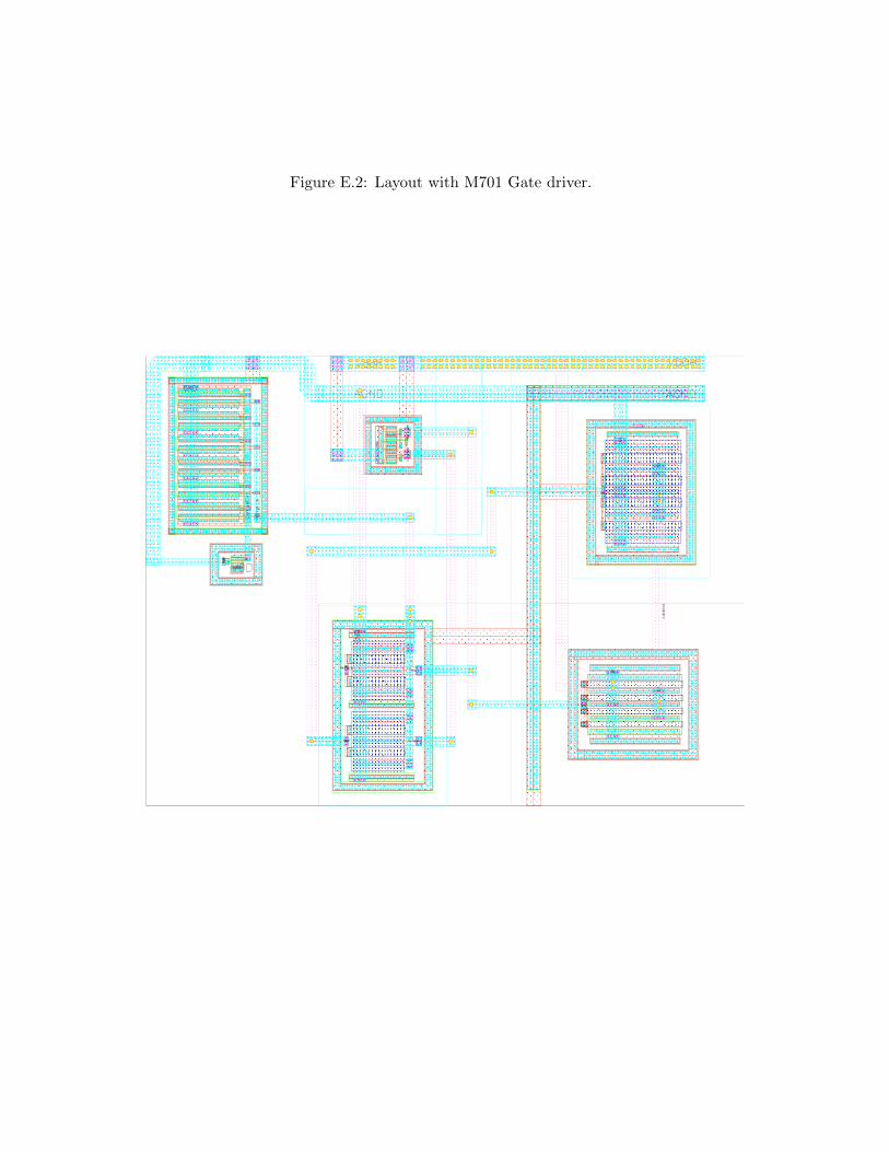
111
111111111111111111111111111111111111
111111111111
111111111111
111111111111
1
1
11
1
1
11
11111
11
11
111111
1111
11111111111111111111111111111111111111111111
11111111
1111111111111111111111111111111111111111111111111
1111111111
1111111111
1111111111
1111111111
22222222222222222222222222222222222222222222222222222222222222222222
222222222222222222222222222222
222222222222222222222222222222
222222222
222222222222
22222222222222222222
222222222222
222222
2222
222222
2222
2222
22
22
2222222222222222
22222222222222222222222222222222
2222
222222222222222222222222222222222222222222222222222222222222222222222222222222222222222222222222222222222222222222222222
22222222
2222222222222222222222222222222222
22
2222222222
2222
222222
22222222222222
22222222222222222222222
22222222222222
222222222222
222222222222
222222222222222222222222222222222222222222222222222222222222222222222222222222222222222222222222222222222222222222222222
2222
2222
2222
22
22
2222
22
22
222222222222222222222222222222222222222222
2
2222222
2222222
22222222222222
22222222222222
222222222222222222
22222222222222
22222222222222
2222222222222222
22222222
22222222
2222222222222222
22222222222222
22222222
2222222
2222222
2222222
222222222222222
2222222
222222222222222222
22222222222222
2222222222222222222222222222
22222222222222
22
22
2222222222
22
22
2222222222
222222
2222
222222
222222
2
2
22
2
2
22
222222
2222222222222222222222222222222222222222
222222222
222222
22222222
22
222222222222222222222222222222
2222
22222222
222222222222
222222
222222222222222222
222222222222
2222222222
22222222222222
222222222222
222222
22
22
2222
222222222222
222222
2222222222222222222222222222222222222222222222222222222222222222222222222222222222222222222222222222222222222222
22
22
22222222222222
22
2222
2222
22
22
2222
22
2222
2222
2222
2222
22
2
2222
2222222
2222
22222222
2222
3333
3333
33333333
333333333333
33
33333333
333333
3333333333
33333333
33333333
33333333333333333
3333
33333333
3333333333333333333333333333
3333333333
3333
3333
3333333
3333
3333333333
333333333333
3333333333333333333333
333333333333333
3333333333333333333333333333333333333333333333333333333
333333333333333333333333333333333333333333333333333333333333333333333333333333333333333333
333333333333333333333333333333333333333333333333333333333333333333333333333333333333333333333
33333333333333333333
33333333
33333333 33
3333333333
3333333333
3333333333333333333333333333333333333333333333333333333333333333
33
3333
3333
333333
3333
333333
3333
3333
33
33
333333333333
33333333
3333
3333
333333
33333333333333333333
333333333333
3333
3333
333333
33
33
3333
33
33
333333333
333333333333333333333333
3333333333333333333333
333333333333333333333333
33
33
3333333333
33
33
3333333333
333333
3333
333333
333333
33333333
3333333333333333333333333333
3333333333333333333333
3333
33
3333
3333
3333
3333
3333
33
3333
3333
3333
3333
3333
333
33
3333
3333
33
333333333
33333333
33
3333333333333333333333
3333
3333
3333
3333
44444444 44444444444444444444
44444444444444444444444444444444444444
4444
44444444
44
444444444444444444
44
44444444444444444444
444444444444444444444444444444
444444444
4444444444444444444444444444444444444444444444
4444444444444444444444444
44444
44444
444444444
4444
4444
44444
44444444
444444444444
44444444
44444
44444
44444
44444
4444
4444444444444
44444
44444
44444
4444444444
44444
44444
44444
44444
44444
44444
44444
44444
444444
444444
44444
44444
4444444444
444
4444
444444444
444444
44444444444444444444
444444
444444
555555555555555555555555555555555555555555555555555555555555555555555555555555555555555555555
555555555555555555555555555555
55555555555555555555
555555
55 555555555
5555
55555555555555555555
5555
5555
555555555555555555555555555555555555555555555555
55
5555
5555555555555555555555555555555555
55555555555555555555555555555555555555555555555555
555555555555
5555555555555555555555555555555555555555
5555555555555555555555555555555555555555
55
5555
5555
1
666666666666666666666666666666666666666666666666666666666666666666666666666666666666
666666666666666666666666666666666666666666666666666666666666
Figure E.2: Layout with M701 Gate driver.
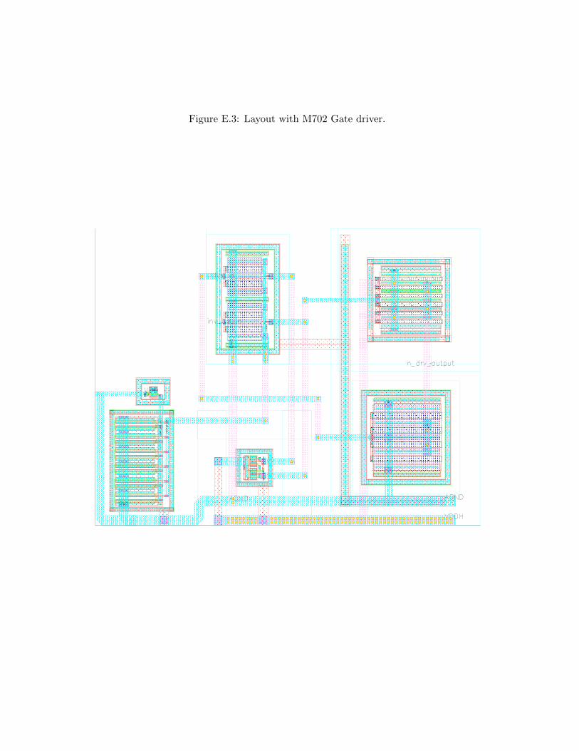
111111
111
111111111
11
111111111111
111111111111
111111111111
111111111111111111111111
111111111111
1
1
11
1
1
11
1111
1111111111
11111111111111111111
11111111111111111111
11111111111111111111
111111111111111111
111111111111111111111111111111111111111111111111111111111111111111111111
1111
1111
11
11111111
11111111111111111111
111111111111111
22222222222222222222222222222222222222222222222222222222222222222222222222222222222222222222222222
22222222222222222222
222222
222222222222222222
2222222222
2222
22
22
2222
22
2222
2222
222222222222222222222222222
222222222222222222222222222
222222222222222222
222222222222222222222222222222222222222222222222222222222222222222222222222222222222222222222222222222222222222222222222222222222222222222222222
2
222222222222222222
222222222222222222
222222222222222222
222222222222222222
222222222222222222
2222
22
22
2222
22
22
2222222222222222
2222222222222222
2222222222222222
22
2222222222222222222222222222222222222222222222222222222222222222222222222222222222222222222222222222222222222222222222222
2222222222222222222222
2222222222222222
2222
2222
22
22222222
22
2222
22
2222
22
222222222222
222222
222222222222
2222222222
22222
222222222222
2222222222
2222222222
22
2222222222222222
222222222222222222222222222222222222222222222222222222222222222222222222222222222222222222222222222222222222222222222222222222222222
22
2
222222222222
22
22
2222
2222
22
22
22
22222
2222
2222
2222222222
222222222222222222222222222222
222222
22222
22
222222
22222222222222
222222
222222
2222
22222222222222
22222222222222222222222222222222222
222222222222222222
22222222222222
22222222222222
22222222
22222222
22222222
222222222222222222222222222222
22222222
2222222
2222222
2222222
222222222222222
2222222
222222222222222222
22222222222222
2222222222222222222222222222
22222222222222
222
222
222
222
222222
222
222
2222
2222
222222
2222
222222
222222
2
2
22
2
2
22
2222222222222222222222222
22222
22222222222222222
22
22222222222222
22222222222222
2222
22222222
2222
3333333333333333333333333333
3333
3333
33333333333333333333
333333
3333
3333
3333333333
3333
3333333333333333
33 3333
3333333333
33
3333
33333333333333
3333
3333333333
333333333333
33333333333
3333333333333333
33333333333333333333333333333333333333333333
3333333333333333333333333333333333333333333333333333333333333333333333333333333333333
33333333333333333333333333333333333333333333333333333333333333
3333333333333333
33333333
33333333333333333
33333
3333333333333333333333333333333333333333333333333333333333333333
3333
33
33
3333
33
3333
3333
3333
33
3333
3333
33
3333
33333333333333333333
333333333333
3333
3333
33
33
3333
3333
33
33
3333333333
333333333333333333
3333
3333
33
3333
33
33333333333333333333333333
3333333333333333333333
33
33
33
3333
3333
33
33
33
33333
3333
3333
3333
3333
3333333333333333333333
3333333333333333333333
333333333333333333333333333333333333333
333
333
333333
333333
333
333
3333
3333
333333
3333
333333
333333
3333333333
3333
3333
33
3333
3333
3333
33
33
3333333333333333333333
33
3333
33 3
333333
333
33333333
4444444444444444444444444444444
44
4444444444
444444 4444444
44444444444
44444444
444444444444444
4444444 4
4444444444444
4444444
4444
44444
4444
444444444444444444444444444444444
4444444
44444444444444444444
44444444444444444444
444444444444444
44444444444444444444
44444
44444
4444444444
44444
44444
4444444444
4444444444
44444
44444
44444
4444
4444
4444
44444444
444444
44444444
444444
444444444444
44444444
44444444
444444
444444
444444
444444
444444
444444444444
444444
444444
444444
444444
444444444
444444
444444
444444
4444444444444444
55555555555555555555555555555555555555555555555555555555555555
555555555555555555555555555555555555
5555
5555
55555555555555555555555555555555555555
55555555555555555555
55555555555555555555
5555
5555
5555555555555555555555555555555555555555
555555
5555555555555555555555555555555555555555555555
55555555555555555555555555555555
55
5
5555555555555555555555555555555555555555555555
55555555555555555555555555555555555555555555
555555555555555555555555555555555555
5555
55
5555
5555
55
5555
11
666666666666666666666666666666666666666666666
666666666666666666666666666666666666666666666666666666
666666666666666666666666666666
666666666666666666666666666666
Figure E.3: Layout with M702 Gate driver.
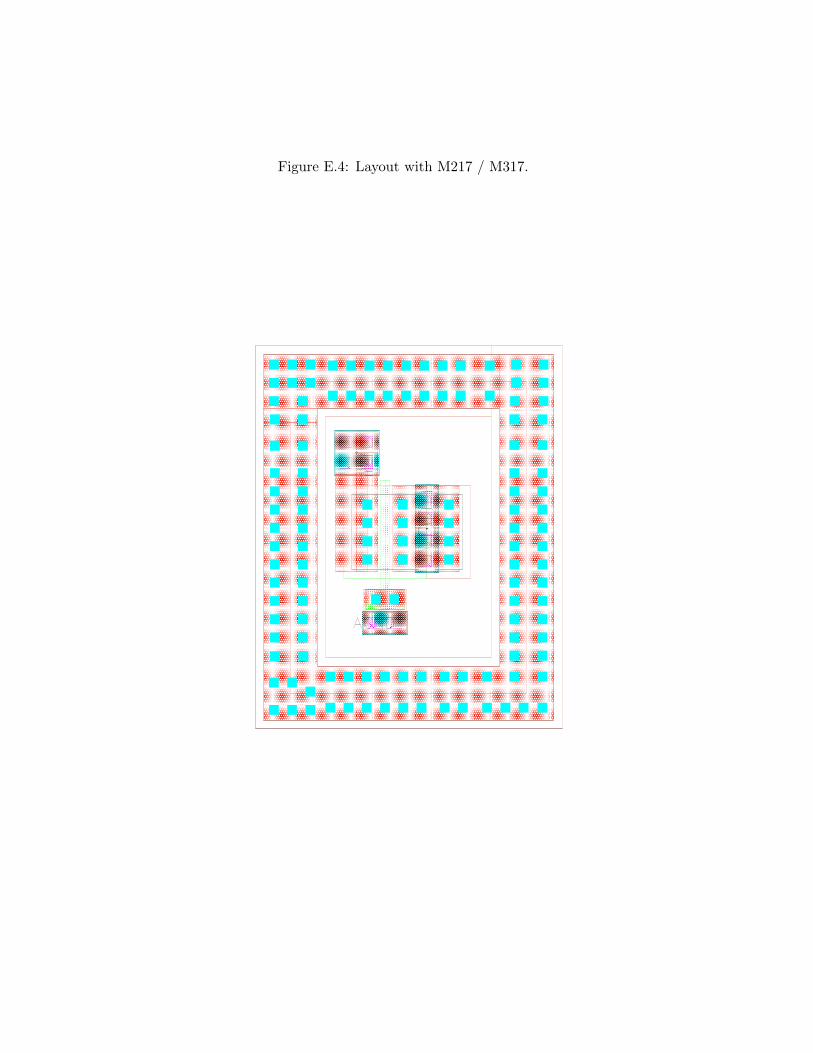
11111111111111111111111111111111
111111111111111
2222222222222222222222222222222222222222222222222222222222222222222222222222222222222222222222222222222222222222222222222222222222222222222222222222222222222222222222222222222222222222222222222222222222222222222222222222222222222222222222222222222222222222222222222222222222222222222222222222222222222222222222222222222222222222222222222222222222222222222222222222222222222222222222222222222222222222222222222222222222222222222222222222222222222222222222222222222222222222222222222222222222222222222222222222222222222222222222222222222222222222222222222222222222222222222222222222222222222222222222222222222222222222222222222222222222222222222222222222222222222222222222222222222222222222222222222222222222222222222222222222222222222222222222222222222222222222222222222222222222222222222222222222222222222222222222222222222222222222222222222222222222222222222222222222222222222222222222222222222222222222222222222222222222222222222222222222222222222222222222222222222222222222222222222222222222222222222222222222222222222222222222222222222222222222222222222222222222222222222222222222222222222222222222222222222222222222222222222222222222222222222222222222222222222222222222222222222222222222222222222222222222222222222222222222222222222222222222222222222222222222222222222222222222222222222222222222222222222222222222222222222222222222222222222222222222222222222222222222222222222222222222222222222222222222222222222222222222222222222222222222222222222222222222222222222222222222222222222222222222222222222222222222222222222222222222222222
222222222222222222222
2222222222222222222222222222222222222222222222222222
222222222222222222222222222222222222
222222222222222222222222222222222222222222222222222222222222222222222222222222222222222222222222222
222222222222222222222222222222222222222222222
222222222222222222
222222222222222222222222222222222
222222222222222222222222222222222222
222222222222222
333333333333333333333
33333333333333333333333333333333333333333333
333333333333333333333333333333333333
333333333333333333333
33333333333333333333333333333333333333333333
333333333333333333333333333333333333
444444
444444
444444444
444444
444444444
444444
4444
4444
444444
444444
555555555555555555555
5555
555555555555555555555555555555555555
55
55555555555555555555555555555555555555555555
Figure E.4: Layout with M217 / M317.
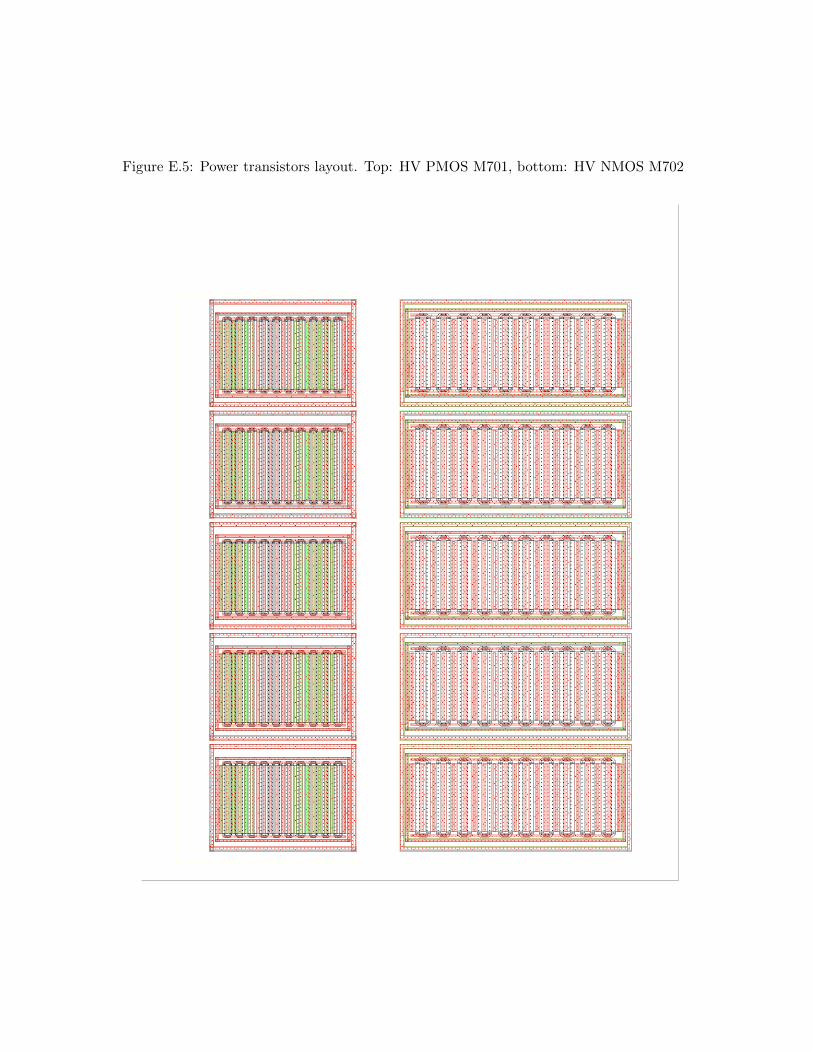
11111111
1111
1111
11
11111111
11111111
11111
11111
11111
11111
11111
11111
11111
11111
11111
11111
11111
11111
11111
11111
11111
11111
11111
11111
11111
11111
11111
11111
11111
111111
111111
111111
111111
111111
111111
111111
111111
111111
111111
111111
111111
111111
111111
111111
111111
111111
111111
111111
111111
111111
111111
111111
111111
111111
11
11
11
11
11
11
11
11
11
11
11
11
11
11
11
11
11
11
11
11
1111 111111
111111
11111111
11 111111
11111111
11 111111
111111
11111111
11 111111
111111
11111111
11 111111
11111111
11 111111
111111
11111111
11 111111
11111111
11 111111
111111
111111 11
11 111111
111111 11
11 111111
111111
1111
11
11 111111
111111
111111
1111
11
11 111111
111111
1111
11
11 111111
111111
111111
1111
11
11 111111
111111
111111
1111
11
11 111111
111111
1111
11
11 111111
111111
111111
1111
11
11 111111
111111
1111
11
11 111111
111111
111111
1111
11
11 111111
111111
1111
11
11 111111
111111
11
11
11
11
11
11
11
11
11
11
11
11
11
11
11
11
11
11111111
111111
1111
111111
111111
111111
11 111111
111111
11 111111
111111
111111 11
111111
111111
1111111
111111
111 111111
111111 11
1111111
111111 11 1
111111 1
111111
111111
111
111111
111111
111111
11
1111
11111
11111
11
11
1111
11111
11111
11
11
11
11
1111
11
11 11111
11111
11
11 11111
11111
11111 1111
11111
11111
1111111
11111
11
11
11 11111
11111 1111
1111111
11111 1111
11
11111 11
11111
11111
11
1111
11111
11111
11111
11
11
1111 111111
111111
11111111
11 111111
11111111
11 111111
111111
11111111
11 111111
111111
11111111
11 111111
11111111
11 111111
111111
11111111
11 111111
11111111
11 111111
111111
111111 11
11 111111
111111 11
11 111111
111111
1111 111111
111111
11111111
11 111111
11111111
11 111111
111111
11111111
11 111111
111111
11111111
11 111111
11111111
11 111111
111111
11111111
11 111111
11111111
11 111111
111111
111111 11
11 111111
111111 11
11 111111
111111
1111111111111111 11 11
11
11
111111
111111
1111
11
111111
111111
111111
11
11 111111
111111
11 111111
111111
111111
11
11
111111
111111
111111
11
111111
111 111111
111111
11
11
1111111
111111
11
11
11
111111
11
111111
111111
111
11
111111
111111
111111
11
11111111
111111
1111
111111
111111
111111
11 111111
111111
11 111111
111111
111111 11
111111
111111
1111111
111111
111 111111
111111 11
1111111
111111 11 1
111111 1
111111
111111
111
111111
111111
111111
11
11
1111
11
11
1111
11
1111
11
11
11
1111
1111111111 1 1
1 1 11 11 1 1 11
11
11
1111
11
11
1111
11
1111
11
11
11
1111
11
11
1111
11
11
11
11
11
11
11
11
11
11
11111111
1111111111
11
11
11
111
1111
11
111
111
1111
11
111
1111
11
111
111
111
1111
11
11
1111
11
11
11
11
11
11
11
11
11
11
11111111
1111111111
11
11
11
11
1111
11
11
1111
11
1111
11
11
11
1111
1111111111 1 1
1 1 11 11 1 1 11
11
11
1111
11
11
1111
11
1111
11
11
11
1111
1111111111 1 1
1 1 11 11 1 1 11
11
2222222
2222222
2222222
2222222
2222222
2222222
2222222
2222222
2222222
2222222
2222222
2222222
2222222
2222222
2222222
2222222
222222
22222222
22222222
22222222
22222222
22222222
22222222
22222222
22222222
22222222
22222222
22222222
22222222
22222222
22222222
22222222
22222222
2222222
2222222
2222222
2222222
2222222
2222222
2222222
2222222
2222222
2222222
2222222
2222222
2222222
2222222
2222222
2222222
222222
22222222
22222222
22222222
22222222
22222222
22222222
22222222
22222222
22222222
22222222
22222222
22222222
22222222
22222222
22222222
22222222
2222222
2222222
2222222
2222222
2222222
2222222
2222222
2222222
2222222
2222222
2222222
2222222
2222222
2222222
2222222
2222222
22222
22222
22222
2222222
2222222
2222222
2222222
2222222
2222222
2222222
2222222
2222222
2222222
22222222
22222222
22222222
22222222
22222222
22222222
22222222
22222222
22222222
22222222
22222222
22222222
22222222
22222222
22222222
22222222
22222222
22222222
22222222
22222222
22222222
22222222
22222222
22222222
22222222
22222222
22222222
22222
22222
22222
22222
22222
22222
22222
22222
22222
22222
22222
22222
22222
22222
22222
22222
22222
22222
22222
22222
22222
22222
22222
22222
22222
22222
22222
22222
22222
2222222
2222222
2222222
2222222
2222222
2222222
2222222
2222222
2222222
2222222
2222222
2222222
2222222
2222222
2222222
2222222
22222
2222222
2222222
2222222
2222222
2222222
2222222
2222222
2222222
2222222
2222222
2222222
2222222
2222222
2222222
2222222
2222222
222222
22222222
22222222
22222222
22222222
22222222
22222222
22222222
22222222
22222222
22222222
22222222
22222222
22222222
22222222
22222222
22222222
222222222
222222222
222222222
222222222
222222222
222222222
222222222
222222222
222222222
222222222
222222222
222222222
222222222
222222222
222222222
222222222
222222222222222
22222
22222
222222
222222
222222
222222
222222
222222
222222
222222
222222
222222
222222
222222
222222
222222
222222
222222
222222
222222
222222
222222
222222
222222
222222
222222
222222
222222
222222
222222
222222
222222
222222
222222222222222
222222222222222
22222
22222
22222
22222
22222
22222
22222
22222
22222
22222
22222
22222
22222
22222
22222
22222
22222
22222
22222
22222
22222
22222
22222
22222
22222
22222
22222
22222
22222
22
22
22
22
22
22
22
22
22
22
22
22
22
22
22
22222222222222222
22
22
22
22
22
22
22
22
22
22
22
22
22
22
22 222222
222222
222222
222222
222222
222222
222222
222222
222222
222222
22222222
222222
222222
222222
222222
222222
222222
222222222
222222222222222
22222222
22222222
22222222
22222222
22222222
22222222
22222222
22222222
22222222
22222222
22222222
22 222222
222222
222222
222222
222222
222222
222222
222222
222222
222222
222222
222222
222222
222222
222222
222222
222222
222222
222222
2222222
2222222
2222222
2222222
2222222
2222222
2222222
2222222
2222222
2222222
2222222
22222
22222
22222
22222
22222
22222
22
22
22
22
22
22
22
22
22
222222222222222222
22222
222222222
222222222
222222222
222222222
222222222
222222222
222222222
222222222
222222222
222222222
222222222
222222
22222
22222
22222
22222
22222
22222
22222
22222
22222
22222
22222
22222
22222
22222
22222
22222
22222
22222
22222
22222
22222
22222
22222
22222
22222
22222
22222
22222
22222
22222
22222
22222
22222
22222
22222
22222
22222
22222
22222
22222
22222
22222
22222
22222
22222
222222
222222
222222
222222
222222
222222
222222
222222
222222
222222
222222
222222
222222
222222
222222
222222
222222
222222
222222
222222
222222
222222
222222
222222
222222
222222
222222
222222
222222
222222
222222
222222222222222
222222222222222
222222
222222
222222
222222
222222
222222
222222
222222
222222
222222
222222
222222
222222
222222
222222
222222
222222
222222
222222
222222
222222
222222
222222
222222
222222
222222
222222
222222
222222
222222
222222
222222222222222
222222222222222
22222222222222222
22
2222222
2222222
2222222
2222222
2222222
2222222
2222222
2222222
2222222
2222222
2222222
22222
22222
22222
22222
22222
22222
222222222
22222222222222
22222222
22222222
22222222
22222222
22222222
22222222
22222222
22222222
22222222
22222222
22222222
22 22222
22222
22222
22222
22222
22222
22222
22222
22222
22222
22222
22222
22222
22222
22222
22222
22222
22222
22222
22 222222
222222
222222
222222
222222
222222
222222
222222
222222
222222
22222222
222222
222222
222222
222222
222222
222222
222222222
222222222222222
22222222
22222222
22222222
22222222
22222222
22222222
22222222
22222222
22222222
22222222
22222222
22 222222
222222
222222
222222
222222
222222
222222
222222
222222
222222
222222
222222
222222
222222
222222
222222
222222
222222
222222
222222222222222222
22
2222
22
22
2222
22
2222
22
22
22
2222
2222222222 2 2
2 2 22 22 2 2 22
22
22
2222
22
22
2222
22
2222
22
22
22
2222
2222222222 2 2
2 2 22 22 2 2 22
22
22
2222
22
22
2222
22
2222
22
22
22
2222
22
22
2222
22
22
22
22
22
22
22
22
22
22
22222222
2222222222
22
22
22
22
2222
22
22
2222
22
2222
22
22
22
2222
2222222222 2 2
2 2 22 22 2 2 22
22
22
2222
22
22
2222
22
2222
22
22
22
2222
2222222222 2 2
2 2 22 22 2 2 22
22
22
22
2
22
22
22
22
22
22
2
22
22
22
22
22
22
22
22
22
22
22
22
222
22
2
2222
2222
2222
2222
2222
Figure E.5: Power transistors layout. Top: HV PMOS M701, bottom: HV NMOS M702
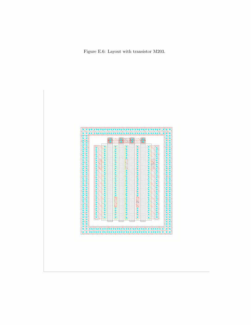
1111
1111
1111
1111
11111111111111111111111111111111111111
11111111111111111111111111111111111111
11111111111111111111111111111111111111
111111111111111111111111111111111111111
11111
11
1111
22222222222222222222222222222222222222222222222222222222222222222222
222222222222222222222222222222222222222222222222222
222222222222222222
2222
222222222222222222222222222222222222222222222222222222222222222222222222222222222222222222222222222222222222222222222222222222222222222222222222222222222222222222222222222222222222222222222222222222222222222222222222222222222222222222222222222222222222222222222222222222222222222222222222222222222222222222222222222222222222222222222222222222222222222222222222222222222222222222222222222222222222222222222222222222222222222222222222222222222222222222222222222222222222222222222222222222222222222222222222
22222222222222222
2222222222222222222222222222222222
22222222222222222222222222222222222222 22 222
22222
22
2222
222222
222
222222
222
222222
222222
Figure E.6: Layout with transistor M203.
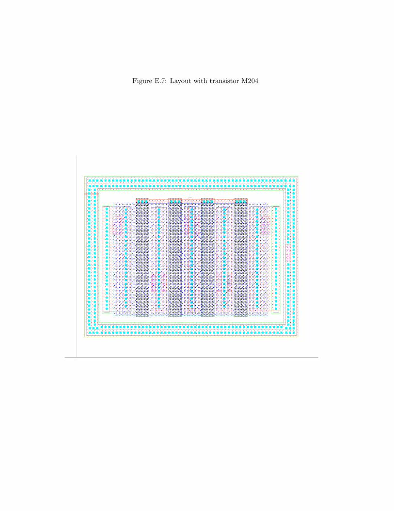
1111111111111111111111111111111111111111111111111111111111111111111111111111111111111111
1111111111111111111111111111111111111111111111111111111111111111111111111111111111111111
1111111111111111111111111111111111111111111111111111111111111111111111111111111111111111
1111111111111111111111111111111111111111111111111111111111111111111111111111111111111111
222222222222222222222222222222222222222222222222222222222222222222222222222222222222222222222222222222222222222222222222
22222222
222222222222222222222222222222222222222222222222222222222222222222222222222222222222222222222222222222222222222222222222222222222222222222222222222222222222222222
2222222222222222222222
22222222222222222222222222222222222222222222222222222222222222222222222222222222
22222222222222222222222222222222222222222222222222222222222222222222222222222222
22222222222222222222222222222222222222222222222222222222222222222222222222222222
222222222222222222222222222222222222222222222222222222222222222222222222222222222222222222222222222222222222222222222222222222222222222222222222222222222222222222222222222222222222222222222222222222222222222222222222222222222222222222222222222222222222222222222222222222222222222222222222222222222222222222222222222222222222222222222222222222222222222222222222222222222222222222222222222222222222222222222222222222222222222222222222222222222222222222222222222222222222222222222222222222222222222222222222222222222222222222222222222222222222222222222222222222222222222222222222222222222222222222222222222222222222222222222222222222222222222222222222222222222222222222222222222222222222222222222222222222222222222222222222222222222222222222222222222222222222222222222222222222222222222222222222222222222222222222222222222222222222222222222222222222222222222222222222222222222222222222222222222222222222222222222222222222222222222222222222222222222222222222222222222222222222222222222222222222222222222222222222222222222222222222222222222222222222222222222222222222222222222222222222222222222222222222222222222222222222222222222222222222222222222222222222222222222222222222222222222222222222222222222222
222222222222
222222222222
22222222
22222222
2222222222
2222222222
2222222222
2222222222
2222
22222222222222222222222222222222222222222222
3333
3333333333333333
3333
3333333333333333
3333333333
3333333333
333333
333333
333333
333333
333333
333333
333333
333333
33333
444444444444444444444444444444444444444444444444444444444444444444444444444444444444444444444444444444444444444444444444444444444444444444444444444444444444444444444444444444444444444444444444444444444444444444444444444444444444444444444444444444444444444444444444444444444444444444444444444444444444444444444444444444444444444444444444444444444444444444444444444444444444444444
444444444444444444444444444444444444444444444444444444444444444444444444444444444444444444444444444444444444444444444444444444444444444444444444444444444444444444444444444444444444444444444444444444444444444444444444444444444444444444444444444444444444444444444444444444444444444444444444444444444444444444444444444444444444444444444444444444444444444444444
Figure E.7: Layout with transistor M204
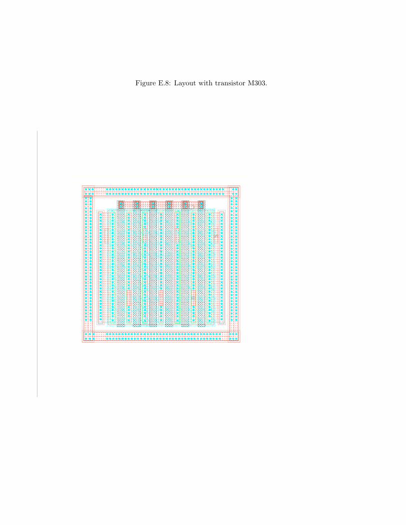
111111111111111111111111111111111111
111111111111111111111111111111111111
111111111111111111111111111111111111
111111111111111111111111111111111111
111111111111111111111111111111111111
111111111111111111111111111111111111
1111
111111
11
11111111
2222222222222222
2222222222222222
2222222222222222222222222222222222222222222222222222222222222222
222222222222222222222222222222222222222222222222
22
2222222222222222222222222222222222222222222222222222222222222222222222222222222222222222222222222222222222222222222222222222222222222222222222222222222222222222222222222222222222222222222222222222222222222222222222222222222222222222222222222222222222222222222222222222222222222222222222222222222222222222222222222222222222222222222222222222222222222222222222222222222222222222222222222222222222222222222222222222222222222222222222222222222222222222222222222222222222222222222222222222
2222222222222222222222222222222222222222222222222222222222
22222222222222222222222222222222
222222222222222222222222222222222
22222
22
22222222
222
222
222222
222222
222
222222
222
22222222222222222222222222
3333333333333333333333333333333333333333333333333333333333333333333333333333333333333333333333333333333333333333333333333333333333333333333333333333333333333333333333333333333333333333333
33333333333333333333333333333333333333333333333333333333333333333333333333333333333333333333333333333333333333333333333
Figure E.8: Layout with transistor M303.
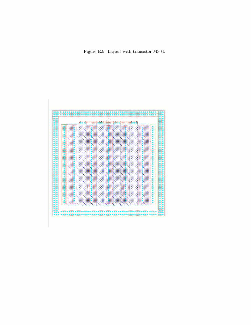
111111111111111111111111111111111111111111111111111111111111111111111111111
111111111111111111111111111111111111111111111111111111111111111111111111111
111111111111111111111111111111111111111111111111111111111111111111111111111
111111111111111111111111111111111111111111111111111111111111111111111111111
222222222222222222222222222222222222222222222222222222222222222222222222222222222222222222222222222222222222222222222222222222222222222222222222
222222222222222222222222222222222222222222222222222222222222222222222222222222222222222222222222
22222222222222222222222222222222222222222222222222222222222222222222222222222222222222222222
222222222222222222222222222222222222222222222222222222222222222222222222222222222222222222222222222222222222222222222222222222222222222222222222222222222222222222222222222222222222222222222222222222222222222222222222222222222222222222222222222222222222222222222222222222222222222222222222222222222222222222222222222222222222222222222222222222222222222222222222222222222222222222222222222222222222222222222222222222222222222222222222222222222222222222222222222222222222222222222222222222222222222222222222222222222222222222222222222222222222222222222222222222222222222222222222222222222222222222222222222222222222222222222222222222222222222222222222222222222222222222222222222222222222222222222222222222222222222222222222222222222222222222222222222222222222222222222222222222222222222222222222222222222222222222222222222222222222222222222222222222222222222222222222222222222222222222222222222222222222222222222222222222222222222222222222222222222222222222222222222222222222222222222222222222222222222222222222222222222222222
2222
22222222222222222222222222222222222222222222222222222222222222222222222222222222222222222222
222222222222222222222222222222222222222222222222222222222222222222222
222222222222222222222222222222222222222222222222222222222222222222222222
222222222222222222222222222222222222222222222222222222222222222222222222 222222222222222222
222222222222222222
222222222222
22222222
22222222
2222
22222222
22222222
22222222
22222222
222222222222222222222222222222222222
333333333333333333333333333333333333333333333333333333333333333333333333333333333333333333333333333333333333333333333333333333333333333333333333333333333333333333333333333333333333333333333333333333333333333333333333333333333333333333333333333333333333333333333333333333333333333333333333333333333333333333333333333333333333333333333333
333333333333333333333333333333333333333333333333333333333333333333333333333333333333333333333333333333333333333333333333333333333333333333333333333333333333333333333333333333333333333333333333333333333333333333333333333333333333333333333333333333333333333333333333333333333333333333333333333333333333333333333333333333333333333333333333
Figure E.9: Layout with transistor M304.
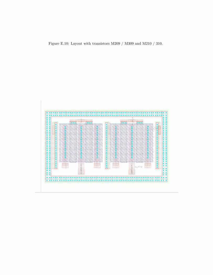
111111111111111111111111111111111111111111111
111111111111111111111111111111111111111111111
111111111111111111111111111111111111111111111
111111111111111111111111111111111111111111111
2222222222222222222222222222222222
2222222222222222222222222222222222
2222222222222222222222222222222222
2222222222222222222222222222222222
222222222222222222222222222222222222222222222
222222222222222222222222222222222222222222222222222222222222222
222222222222222222222222222222222222222222222222222
222222222222222222222222222222222222222222222
222222222222222222222222222222222222222222222222
222222222222222222
222222222
2222222222222222222222222222222222
2222222222222222222222222222222222
222222222222222222222222222222222222222222222222222222222222222222222222222222222222222222222222222222222222222222222222222222222222222222222222222222222222222222222222222222222222222222222222222222222222222222222222222222222222222222222222222222222222222222222222222222222222222222222222222222222222222222222222222222222222222222222222222222222222222222222222222222222222222222222222222222222222222222222222222222222222222222222222222222222222222222222222222222222222222222222222222222222222222222222222222222222222222222222222222222222222222222222222222222222222222222222222222222222222222222222222222222222222222222222222222222222222222222222222222222222222222222222222222222222222222222222222222222222222222222222222222222222222222222222222222222222222222222222222222222222222222222222222222222222222222222222222222222222222222222222222222222222222222222222222222222222222222222222222222222222222222222222222222222222222222222222222222222222222222222222222222222222222222222222222222222222222222222222222222222222222222222222222222222222222222222
222222
222222
222222222222222222222222222222222222222222222222222
22222222
22222222
22222222
222222
222222
222222
222222
222222
222222
222222
222222
22222222
333333333333333333333333333333333333333333333333333333333333333333333333333333333333333333333333333333333333333333333333333333333333333333333333333333333333333333333333333333333333333333333333333333333333333333
333333333333333333333333333333333333333333333333333333333333333333333333333333333333333333333333333333333333333333333333333333333333333333333333333333333333333333333333333333333333333333333333333333333333333333
Figure E.10: Layout with transistors M209 / M309 and M210 / 310.
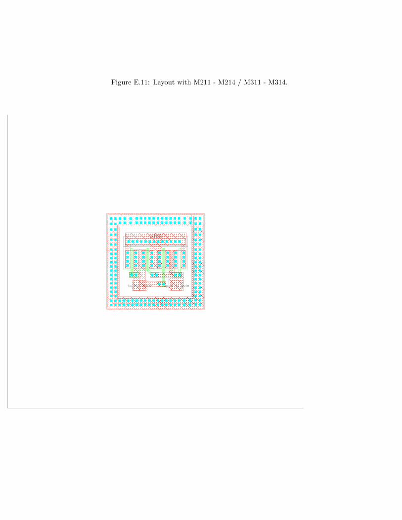
11111111
11111
1111
1111
1111
11 11222222222222
22222222
2222222222222222222222222222222222222222222222222222222222222222222222222222222222222222222222222222222222222222222222222222222222222222222222222222222222222222222222222
222222222222222222
22222222222
22
222222222222222222
22 2222
22222222
222222
222222
222222
222222
222222
222222
22222222
2222
22 22
222222
2222
222222222
2222
2222
Figure E.11: Layout with M211 - M214 / M311 - M314.
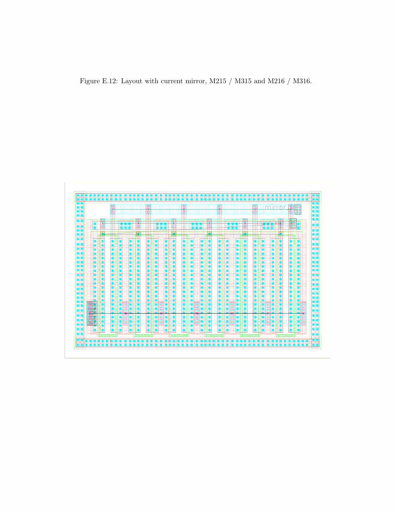
11111111111111111111111111111111111111111111111111111111111111111111111111111111
1111111111111111111111111111111111111111111111111111111111111111111111111111111111111111111111111111
11111111111111111111111111111111111111111111111111111111111111111111111111111111
11111111111111111111111111111111111111111111111111111111111111111111111111111111
1111111111111111111111111111111111111111111111111111111111111111111111111111111111111111111111111111
1111111111111111111111111111111111111111111111111111111111111111111111111111111111111111111111111111
1111
1111
1111
11
1111
1111
222222222222222222222222222222222222222222222222222222222222222
222222222222222222222222222222222222222222
222222222222222222222222222222222222222222222222222222222222222222222222222222222222
222222222222222222222222222222222222222222222222222222222222222
2222222222222222222222222222222222222222222222222222222222
222222222222222222222222222222222222222222222222222222222222222222222222222222222222
22222222222222222222222222222222222222222222
222222222222222222222222222222222222222222222222
222222222222222222222222222222222222222222222222
222222222222222222222222222222222222222222222222
222222222222222222222222222222222222222222222222
222222222222222222222222222222222222222222222222222222222222222222222222222222222222
222222222222222222222222222222222222222222222222
22222222222222222222222222222222222222222222
22222222222222222222222222222222222222222222
222222222222222222222222222222222222222222222222222222222222222
22222222222222222222222222222222222222222222
222222222222222222222222
2222222222222222222222
2222222222222222222222222222222222222222222222222222222222222222222222222222222222222222222222222222222222222222222222222222222222222222222222222222222222222222222222222222222
222222222222222222222222222222222222222222222222222222222222222222222222222222222222222222222222222222222222222222222222222222222222
22222222222222222222222222222222222222222222
222222222222
222222222222
222222222222
222222222222
222222222222
222222
222222222222
222222222222
222222
222
222222222222
222222222
222222222222
222222222222
2222
2222
2222
22
2222
2222333333333333333333333333333333333333333333333333333333333333333333333333333333333333333333333333333333333333333333333333333333333333333333333333333333333333333333333333333333333333333333333333333333333333333333333
333333333333333333333333333333333333333333333333333333333333333333333333333333333333333333333333333333333333333333333333333333333333333333333333333333333333333333333333333333333333333333333333333333333333333333333333333333333333333333333333
333333333333
333333333333
333333333333
333333333333
333333333333
333333
333333333333
333333333333
333333
333333
333333333333
333333333
333333333333
333333333333
333333333333
333333333333
444444
44444444
444
4444
444
4444
444444
44444444
444
4444
444
4444
444444
44444444
444444
44
44
44444
4444
4444
444
44
444
4444
444444
4455 55 55 5555 55 55
555555
55 55 55 55 55 5555
55555555555555555555
5555
5555
55555555
5555
5555
5555
5555
555555555555
Figure E.12: Layout with current mirror, M215 / M315 and M216 / M316.
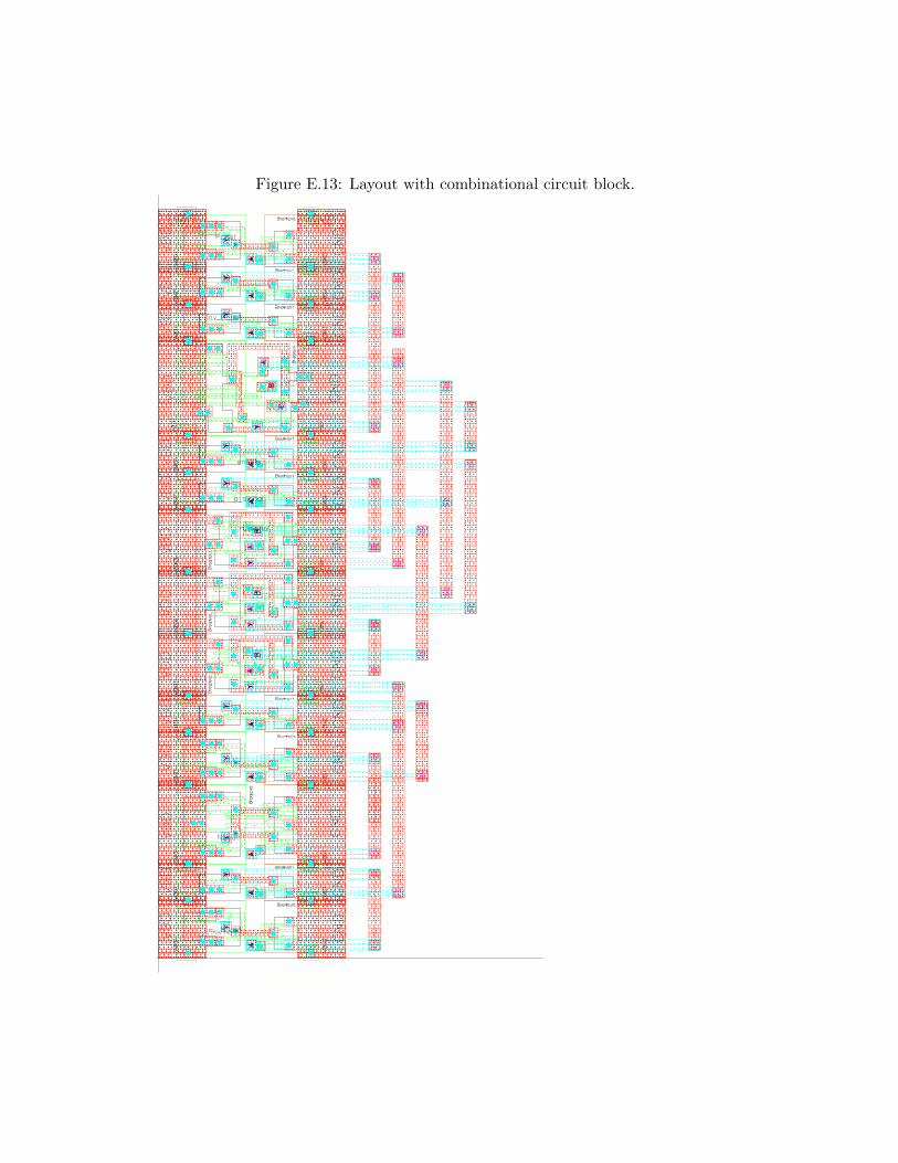
11111111111111111111111111111111
111111111111111111111111
11111111111111111111111111111111
111111111111111111111111
111111111111111111111
111111111111111111111
1111111111111111111111
111111111111111111111111
111111111111111111111111111111
111111111111111111111111111111111111
111111111111111111111111111111111111
1111111111111111
111111111111111111111111
1111111111111111111111111111111111111111
1111111111111111111111111111111111111111 22
222222
22222222222222222222
22
222222222222222222222222
2222222222222222
222222
22222222
222222
22222
2222
2222
222222222222222222
2222222222
222222222222
222222
222222222222222222222222222222
2222222222222222222222222222
22
2
22
2
2222
22
2
2222
22
22
22
22
22
2222
2
22
2222
22
22
2222
2
2
2
2222
22
2
22
22
2222
222222222222222222222222222222
2222222222222222
2222
222222222222222222222222222222
2222 2222
2222 2222
22222222222222222222
22222222
2222222222222222222222
22222222
22222222
2222 2222
22222222222222222222
22222222
2222
22222222222222222222
2222 2222
22222222
22222222
22222222222222222222
22222222
2222
22222222222222222222
2222 2222
2222 2222
2222222222222222222222222222
222222222222222222222222222222
222222
2222
222222222222222222222222222222
22222
22222222
22222222
2222 2222
2222222222222222222222222
222222222
22222222222222222222
2222222222222222222222222
2222 2222
2222 2222
22222222222222222222
22222222222
222222222222222
22222222222222222222
22222222
22222222
22222222
22222222
2222222222222222222222222
222222222222222222
22222222222222222222
2222222222222222222222222
2222 2222
2222 2222
222222222222222
22222222
2222
2222222222222222222 2222
2222 2222
22222222222222222222
22222222
2222
222222222222222222222222 2222
2222 2222
22222222222222222222
22222222
2222
222222222222222222222222 2222
2222 2222
222222222222222
222222222222222
22222222222222 2222
22222222
22222222
222222222222222
22222222
2222
2222222222222222222 2222
2222 2222
222222222222222
22222222
2222
22222222222222222222222
22222222
2222 2222
22222222
22222222
222222222222222222222222
222222222222222222222222
22222222222222222222
22222222222222222222
22222222222222222222
22222222222222222222
2222222222222222
2222222222222222
2222222222222222222222222222
2222222222222222222222222222
22222222222222222222
22222222222222222222
222222222222222222222222
222222222222222222222222
22222222222222222222
22222222222222222222
222222222222
222222222222
2222222222222222
2222222222222222
2222222222222222
2222222222222222
2222222222222222
2222222222222222
222222222222
2222222222222222
222222222222
222222222222222233333333333333333333333333
33333333333333333333333333333333
333333333333333333333333333333
333333333333333
3333333333333333333333
33333333333
333333
3333333333333
3333333333333333333333
3333333333333333333333333333
3333333333333333333333333333
33333333333333333333
3333333333333333333333
333333333333333333
33333333333333333333
3333333333
33333333333333333333
333333333333333333
3333333333333333333333
333333333333
333333333333333333333333
333333333333333333
33333333333333333333333333
3333333333333333333333
333333333333333333
333333333
333333333
333333333
333333333
333333333333
3333
3333
3333
33
3333
33
3
3333
33
33
3333
33
33
3333
33
33
3333
33
33
3333
3
3
3
3333
33
3
33
33
3333
33333
3
33333
3
33333
3
33333
3
3333
3
3333
33
33333333
333333
333333333333
33333
3
3333
3
3333
333
3
33333
333333
3
33
33
3
33
3333
3333
3333
33
3333
33333
3
33333
3
33333
3
3
3333
3333
33
33333333
333333
3333
3333
3333
33
3333
3
3333
3
3333
333
33
3333
33
3333
4
44
4
44
44
4
44
44
4
4
44
44
4444
4
44
4444
444
44
4
4
4
4444
44
4
44
44
44
444
444
44444
4
4444
4
4
4444
4
444
444
444444
44444
4
444
44444
4
44444
444
4
Figure E.13: Layout with combinational circuit block.
References
[1] G. Ter Haar, “Ultrasound focal beam surgery,” Ultrasound in Medicine and Biology, vol. 21, no.
9, pp. 1089–1100, 1995.
[2] T. Hall and C. Cain, “A low cost compact 512 channel therapeutic ultrasound system for
transcutaneous ultrasound surgery,” AIP Conference Proceedings, vol. 829, no. 1, pp. 445–449,
May 2006.
[3] N. Yu and R. Riener, “Review on MR-compatible robotic systems,” in The First IEEE/RAS-
EMBS International Conference on Biomedical Robotics and Biomechatronics, 2006. BioRob 2006,
pp. 661–665.
[4] F. Ellinger “Power Amplifiers ” in Radio frequency Integrated Circuits and Technologies, Berlin;
New York: Springer, 2007, ch. 9, pp. 307–327.
[5] M. K. Kazimierczuk, RF Power Amplifiers, Chichester, West Sussex, U.K.: Wiley, 2008.
[6] L. Svilainis, V. Dumbrava and G. Motiejunas, “Optimization of the ultrasonic excitation stage,
” 30th International Conference on Information Technology Interfaces, 2008. ITI 2008. 2008. pp.
791–796.
[7] Y. Mizutani, T. Suzuki, H. Ikeda and H. Yoshida, “Automatic frequency control for maximizing
RF power fed to ultrasonic transducer operating at 1 MHz,” Thirty-First IAS Annual Meeting in
Industry Applications Conference, 1996, IAS ’96, vol. 3, pp. 1585–1588
[8] K. Agbossou, J. Dion, S. Carignan, M. Abdelkrim and A. Cheriti, “Class D amplifier for a power
piezoelectric load,” IEEE Transactions on Ultrasonics, Ferroelectrics and Frequency Control, vol.
47, pp. 1036–1041, 2000.
REFERENCES 107
[9] L. Yang, L. Xu, T. Yang and B. Zhang, “Class D power amplifier for audio beam system,”
International Conference on Mechatronics and Automation, 2007. ICMA 2007. 2007. pp. 3469–
3474.
[10] S. C. Tang and G. T. Clement, “A harmonic cancellation technique for an ultrasound transducer
excited by a switched-mode power converter,” in Proc. IEEE Ultrasonics Symp., 2008, pp. 2076–
2079.
[11] H. L. Cheng, C. A. Cheng, C. C. Fang and H. C. Yen, “Single-switch high power factor inverter
for driving piezoelectric ceramic transducer”, International Conference on Power Electronics and
Drive Systems, 2009. PEDS 2009. pp. 1571–1576.
[12] G. Lewis and W. Olbricht, “Design and characterization of a high-power ultrasound driver with
ultralow-output impedance,” Review of Scientific Instruments, vol. 80, no. 11, p. 114704, 2009.
[13] W. T. Ang, C. Scurtescu, W. Hoy, T. El-Bialy, Y. Y. Tsui, and J. Chen, “Design and imple-
mentation of therapeutic ultrasound generating circuit for dental tissue formation and tooth-root
healing,” IEEE Trans. on Biomedical Circuits and Systems, vol. 4, no. 1, pp. 49–61, 2010.
[14] A. Arnau, Piezoelectric Transducers and Applications. 2nd ed. New York: Springer, 2008. ch.1,
p. 18, p. 23, ch.18, sec. 18.3, pp. 467–472.
[15] “IEEE Standard Definitions and Methods of Measurement for Piezoelectric Vibrators,” 1966.
[16] D. M. Pozar, “Transmission Line Theory,” in Microwave Engineering, 3rd ed. New Jersey: John
Wiley and Sons, 2005, p. 77.
[17] H. Koizumi; T. Suetsugu; M. Fujii; K. Shinoda; S. Mori; K. Iked, “Class DE high-efficiency
tuned power amplifier,” in IEEE Transactions on Circuits and Systems I: Fundamental Theory
and Applications, vol.43, no.1, pp.51–60, Jan 1996.
[18] Foundry Design Kit 0.8 µm 5/20V CMOS User’s Guide, Dalsa Semiconductor Inc. Document
No., DK08EUG01.09, 2007.
[19] M. Albulet, “An exact analysis of Class-DE amplifier at any output Q,” IEEE Trans. Circuits
and Systems I, vol. 46, no. 10, pp. 1228–1239, Oct 1999.
REFERENCES 108
[20] H. Sekiya, T. Negishi, T. Suetsugu, and T. Yahagi, “Operation of Class DE amplifier outside
optimum condition,” in Proc. of IEEE International Symposium on Circuits and Systems (ISCAS
2006), May 2006, p. 4.
[21] H. Ballan and M. Declercq, “High-Voltage Analog and Digital Output Interfaces, ”in, High Voltage
Devices and Circuits in Standard CMOS Technologies, Dordrecht, Netherlands: Kluwer Academic
Publishers, 1999, ch. 6, pp. 181–207.
[22] S. Kang and Y. Leblebici, “MOS Inverters: Switching Characteristics and Interconnect Effects,”
in CMOS Digital Integrated Circuits: Analysis and Design, 3rd ed. Boston, MA: McGraw-Hill,
2003, ch.6, sec 6.3, pp. 220–228.
[23] Foundry Design Kit 0.8 µm 5/20V CMOS Cell Library, Dalsa Semiconductor Inc., Document
No. DK08EDS01.04, 2005. 34 D. Clein 1958-, CMOS IC Layout : Concepts, Methodologies, and
Tools /. Boston : Newnes, c2000.
[24] “Audit Checklists”, in CMOS IC Layout: concepts, methodologies, and tools. Boston, MA:
Newnes, 2000, pp. 246–247.


![High Intensity Focused Ultrasound Facial Skin Lifting · HIFU Mechanism HIFU [High Intensity Focused Ultra-sound] • Non-invasive treatment with thermal energy that focused ultrasound](https://img.dokumen.tips/doc/110x75/5fd8347ce1f6a6277a18bb54/high-intensity-focused-ultrasound-facial-skin-hifu-mechanism-hifu-high-intensity.jpg)


![Review of Laser-Generated Ultrasound Transmitters and ...€¦ · High intensity focused ultrasound (HIFU) is valuable for therapeutic applications [15,16]. Its applications featuring](https://img.dokumen.tips/doc/110x75/5f0d02697e708231d4383a2a/review-of-laser-generated-ultrasound-transmitters-and-high-intensity-focused.jpg)