Embed Size (px)
Citation preview
8 QEX – March/April 2014
Michael Dzado, ACØHB
2601 Salem Circle, Marion, IA 52302; [email protected]
An Eight Channel Remote Control Antenna Selector
Select between eight antennas or feed one antenna to any of up to eight radios. With better than 70 dB of port-to-port isolation, you can be sure
the signal is going where you want it to.
A few years ago, my friend Joe Spinks, AAØKW, and I started building and experimenting with Double Bazooka antennas. I decided to build two 20 m and two 40 m antennas for my antenna farm. My plan was to deploy a 20 and 40 m Double Bazooka facing East-West and a 20 and 40 m Double Bazooka facing North-South. These, along with a vertical antenna and two G5RV antennas I already had mounted, quickly gave me a cabling and switching problem. Also, Joe pointed out that my wife may not appreciate me punching seven more holes in our house and running a sizable bundle of coax across my basement to my station. Even if I could do all that, manual switching wasn’t practical between that many antennas. I would be constantly connecting and disconnecting antennas when I wanted to change directions or bands.
That’s when I decided to design a remote control antenna selector to select between eight antennas. I am currently a Systems Engineer but have degrees in both Electrical Engineering and Software Engineering. In addition, I have electronic circuit design and printed circuit board layout experience. Joe is also an electrical engineer, and has designed automatic antenna tuners for our company and has extensive RF circuit design experience. So creating and testing a viable design was not a technical concern. The main question then became, what improvements could be made over the existing products. The answer came quickly: Isolation between the selected and other antennas! Wouldn’t it be nice to select one antenna and not get interference from another antenna?
We achieved greater than 70 dB of isolation between antenna ports, as shown in the test plots included with this article. There are several design techniques that helped us achieve this kind of isolation: Two relays were used in each signal path to double isolate the antenna from the radio input. The traces that make up the RF path were designed as a coplanar waveguide. The RF connector placement on the circuit board was tightly controlled to be symmetrical to make the RF electrical paths identical. RF trace routing followed good design practices
by limiting angles to 45°. Control traces were routed on the bottom of the circuit board to maximize ground plane continuity. For our switch, we selected control trace widths of 15 mils for better current capacity.
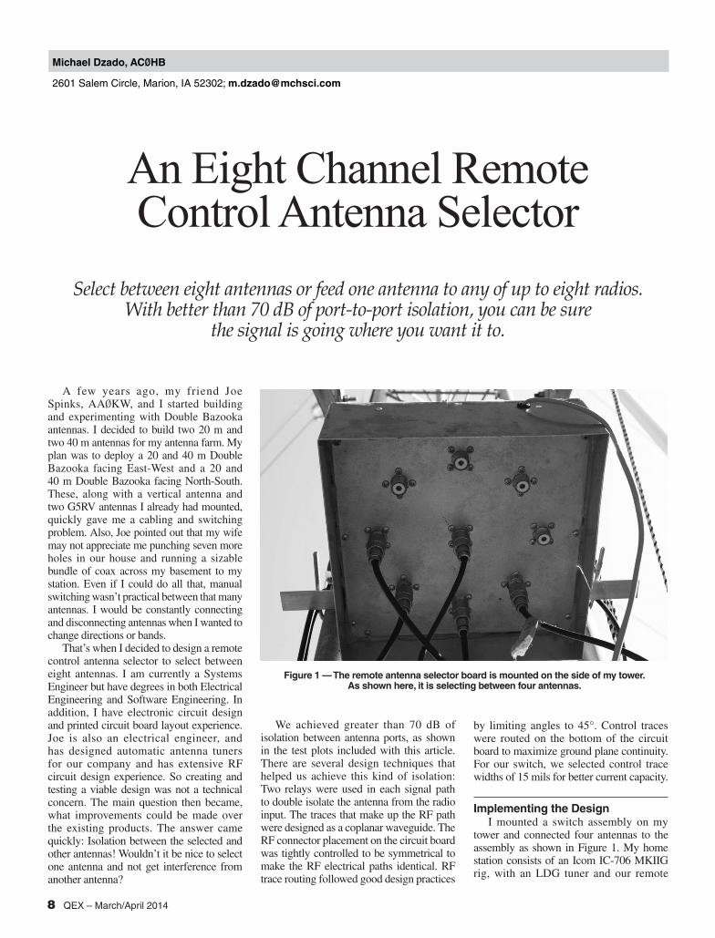
Implementing the DesignI mounted a switch assembly on my
tower and connected four antennas to the assembly as shown in Figure 1. My home station consists of an Icom IC-706 MKIIG rig, with an LDG tuner and our remote
Figure 1 — The remote antenna selector board is mounted on the side of my tower. As shown here, it is selecting between four antennas.
QEX – March/April 2014 9
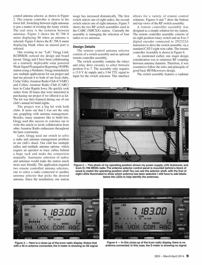
control antenna selector, as shown in Figure 2. The remote controller is shown in the lower left. Switching between eight antennas is just a matter of twisting the rotary switch. The real story is the isolation between antennas. Figure 3 shows the IC-706 S meter displaying S6 when an antenna is selected. Figure 4 shows the IC-706 S meter displaying blank when an unused port is selected.
One evening in my “Lab,” Gregg Lind, KCØSKM, noticed my design and board layout. Gregg and I have been collaborating on a remotely deployable solar powered Weak Signal Propagation Reporting (WSPR) station using a Netduino. Gregg immediately saw multiple applications for our project and had me present it to both of our local clubs, Cedar Valley Amateur Radio Club (CVARC) and Collins Amateur Radio Club (CARC) here in Cedar Rapids Iowa. He quickly took orders from 20 hams that were interested in purchasing our project if we offered it as kit. The kit was then featured during one of our club’s annual kit build nights.
The project was a big hit with both clubs. It turns out that I was not the only one grappling with antenna management. Besides, many amateurs like to build kits. Gregg used this success to convince me to write this article to invite collaboration from other Amateur Radio enthusiasts throughout the ham community.
Later, Gregg used our switch to solve a radio and antenna management problem in our club’s shack. Our club has multiple radios and multiple antenna options, which require an operator to trace cables behind a huge rack and make the connection manually. Automatic selection of radios and antennas would make the station much more user friendly. The application required two remote controlled antenna selectors, one to select a radio connected to another antenna selector that picks the desired antenna. Since the installation, our station
Figure 2 — This photo of my operating position shows my power supply, LDG Autotuner, and Icom IC-706 MKIIG radio. The antenna selector control panel is mounted behind a block of wood to match the operating position shelf. You can see the selector shaft, with the first of eight LEDs illuminated to show which antenna has been selected. I still have to add labels
below the LEDs to help identify the antennas.
Figure 3 — Here is a close-up of the Icom radio display. Notice that with a 40 m antenna connected, the S meter is showing an S6 signal.
Figure 4 — In this close-up of the Icom radio display, there is no antenna connected. In this case, the S meter is showing no signal.
usage has increased dramatically. The first switch selects one of eight radios, the second switch selects one of eight antennas. Figure 5 shows the two RF switch assemblies used in the CARC (NØCXX) station. Currently the assembly is managing the selection of four radios to six antennas.
Design DetailsThe remote control antenna selector
consists of a switch assembly and an optional remote controller assembly.
The switch assembly contains the relays and relay drive circuitry to select between position 0 to 7. The assembly only requires a 13.8 V dc supply and a 3-bit TTL signal to input for the switch selection. This interface
allows for a variety of remote control solutions. Figures 6 and 7 show the bottom and top views of the RF switch assembly.
A remote controller assembly was designed as a simple solution for my station. The remote controller assembly consists of an eight position rotary switch and an 8-to-3 digital encoder connected to 2N2222A transistors to drive the switch assembly via a standard CAT-5 eight wire cable. The remote controller Assembly is shown in Figure 8.
As mentioned earlier, one major design consideration was to minimize RF coupling between antenna channels. Therefore, it was essential to follow the rules and principals of good basic RF/Microwave design.
The switch assembly features a coplanar

10 QEX – March/April 2014
Figure 5 — This photo shows the two RF switch assemblies used in the Collins
Amateur Radio Club (NØCXX) station. The assembly is managing the selection of four radios to six antennas in the club station.
Figure 6 — Here is a close-up of the SO-239 connector side of the antenna selector circuit board.
Figure 7 — This photo shows the relays and the circuit board traces that form the coplanar waveguide.
Figure 8 — This photo shows the antenna selector control board.
waveguide design for all RF traces, tuned to a 50 W impedance with ground plane stitching that ensures maximum isolation between ports.
Complete impedance (Z0) matching (50 W in to 50 W line to 50 W out) minimizes return loss and SWR. A coplanar waveguide design was chosen so that the trace impedance on the circuit board could be matched to the input and output impedances. In a coplanar waveguide design, Z0 is a function of signal conductor width & thickness and a function of the dielectric constant (er) of the material surrounding the signal conductors.
Signal return currents follow the path of least impedance. In high frequency circuits this equates to the path of least inductance. Stitching the ground planes with vias every 0.1 inches or so around each RF trace helps minimize the inductance in the signal return path by virtually creating a waveguide on the circuit board.
The RF connectors were placed symmetrically around the output connector (located in the center of the assembly) to ensure an equal electrical length for each RF path. Typical isolation measured between ports is greater than 70 dB.
Extensive RF decoupling on the power and control lines was added to provide maximum RF decoupling from the control signals. I added transient-voltage-suppression diodes (Transorbs) on all input control lines for good surge protection.
The project begins with a schematic program to capture the logical design. I chose TinyCAD for my schematic capture and Free PCB for the circuit board layout and trace routing. Both tools are easy to use and use the same net list format.1, 2
The switching relay is the heart of this design. We chose an Omron Electronics Inc G6RN-1-DC12, which is a sealed double pole double throw (DPDT) relay with 8 A silver
1Notes appear on page 17.
QEX – March/April 2014 11
QX1403-Dzado09
ANT_1J1
1
2
1
2
J11
1 2
2
C3 NC
4 NO 2
C3 NC
4 NOSwitch 1
J9
ANT_OUT
5 pFC13
0.01 μFC11
K11
0.01 μFC12
K12
12 V SW_1
5–
5–
1 +
1 +
QX1403-Dzado10
VCC16
Y015
Y114
Y213
Y312
Y411
Y510
Y69
U2
74HC238N
IN 01
IN 12
IN 23
IN 34
IN 45
IN 56
IN 67
IN 78
OUT 0
16OUT 1
15OUT 2
14OUT 3
13OUT 4
12OUT 5
11OUT 6
10OUT 7
U3
ULN2008A
GND9
COM
18
17
5 V
A1
B2
C3
–G–2A4
–G–2B5
8
G16
7
5 V
Y7
GND
R15.1 kΩ
C10.01 μF
R15.1 kΩ
C20.01 μF
R15.1 kΩ
C30.01 μF
11
22
33
44
55
66
77
88
11
22
33
44
55
66
77
88
12 V
D51N4001
D4D3D2
D1
12 V
C40.1 μF
5 V
C50.1 μF
U178L05
1
2
3OutInGnd
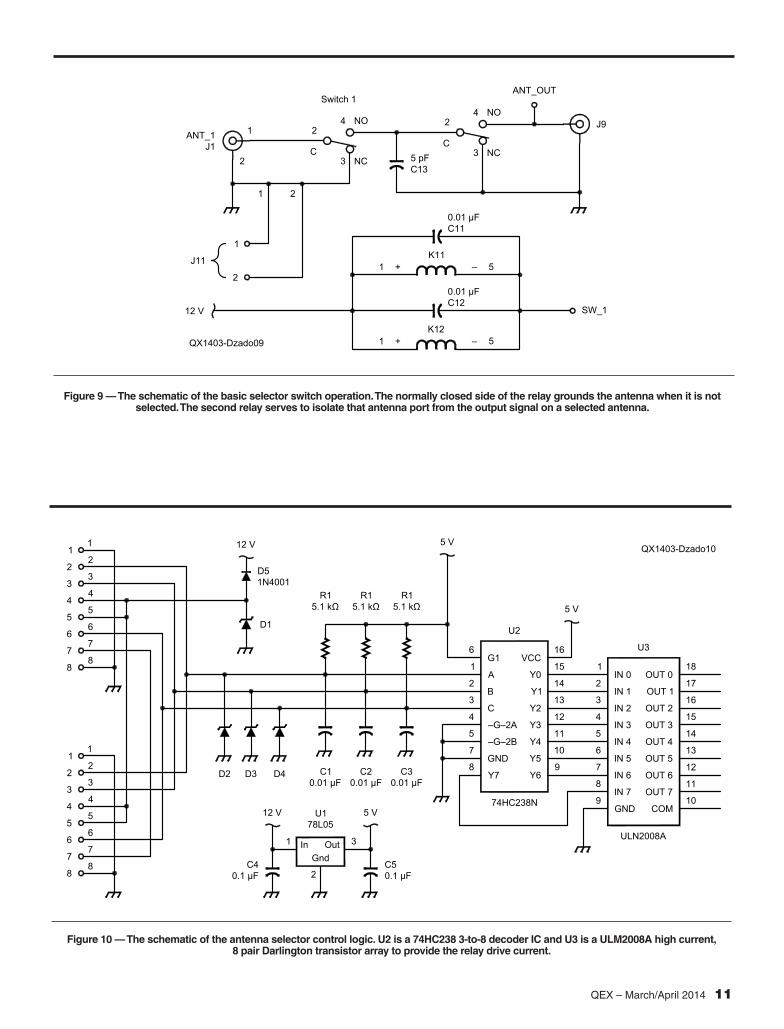
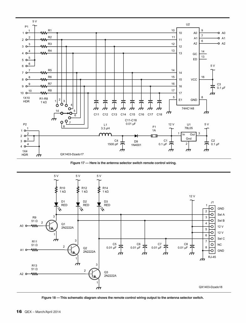
Figure 10 — The schematic of the antenna selector control logic. U2 is a 74HC238 3-to-8 decoder IC and U3 is a ULM2008A high current, 8 pair Darlington transistor array to provide the relay drive current.
Figure 9 — The schematic of the basic selector switch operation. The normally closed side of the relay grounds the antenna when it is not selected. The second relay serves to isolate that antenna port from the output signal on a selected antenna.
12 QEX – March/April 2014
over gold contacts. The contact capacity is more than adequate for our design. We chose to double isolate each RF port by using two relays in each path. As shown in Figure 9, the first relay will ground the antenna input when de-energized. The second relay simply isolates the RF port from the output.
The switch control logic incorporates a simple 3-to-8 decoder (74HC238) and a high current, eight-pair Darlington transistor array (ULM2008A) to provide the relay drive current, as seen in Figure 10.
Topologically speaking, a coplanar waveguide design offers better isolation between signals versus a microstrip design. Even though a microstrip design is easier to layout, Joe and I opted for maximum isolation between antennas.
The RF path design starts with the basic power equation to determine the trace width to handle the transmit current.
P = I2 Z0 [Eq 1]
then solving for I:
0
PIZ
= [Eq 2]
Then for a 100 W transmitter into a 50 W load we have:
100 W 2 A 1.4 A50
I = = =W
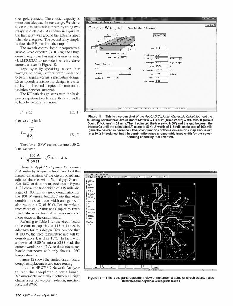
Using the AppCAD Coplanar Waveguide Calculator by Avago Technologies, I set the known dimensions of the circuit board and adjusted the trace width, W, and gap, G, until Z0 = 50 W, or there about, as shown in Figure 11.3 I chose the trace width of 115 mils and a gap of 100 mils as a good combination for the 100 W circuit boards. Note that other combinations of trace width and gap will also result in a Z0 of 50 W. For example, a trace width of 125 mils and a gap of 250 mils would also work, but that requires quite a bit more space on the circuit board.
Referring to Table 1 for the circuit board trace current capacity, a 115 mil trace is adequate for this design. You can see that at 100 W, the trace temperature rise will be considerably less than 10°C. In fact, with a power of 1000 W into a 50 W load, the current would be 4.47 A, so these traces can handle that power with only about a 10°C temperature rise.
Figure 12 shows the printed circuit board component placement and trace routing.
I used an HP-8753D Network Analyzer to test the completed circuit board. Measurements were taken between all eight channels for port-to-port isolation, insertion loss, and SWR.
Figure 11 —This is a screen shot of the AppCAD Coplanar Waveguide Calculator. I set the following parameters: Circuit Board Material = FR-4, W (Trace Width) = 125 mils, H (Circuit Board Thickness) = 62 mils. Then I adjusted the trace width (W) and the gap between the traces (G) until the calculated Z0 came to 50 W. A width of 115 mils and a gap of 100 mils gave the desired impedance. Other combinations of those dimensions may also result in a 50 W impedance, but this combination gave a reasonable trace width for the power
handling capability that I wanted.
Figure 12 — This is the parts-placement view of the antenna selector circuit board. It also illustrates the coplanar waveguide traces.
QEX – March/April 2014 13
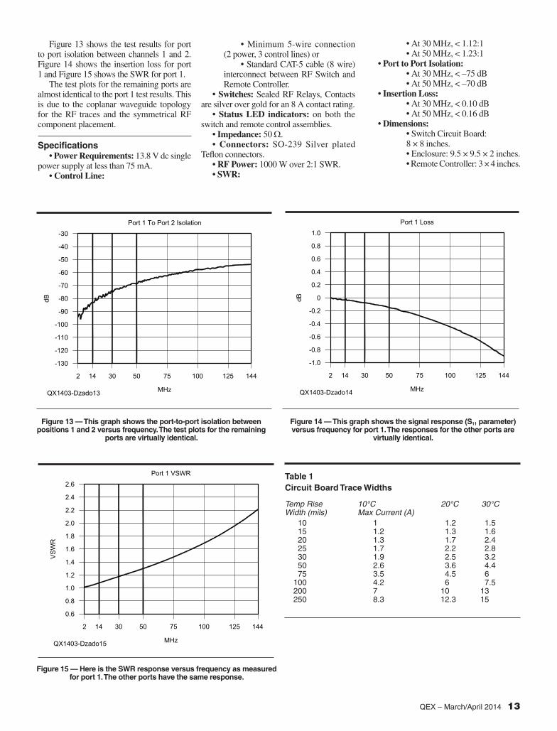
Table 1Circuit Board Trace Widths
Temp Rise 10°C 20°C 30°C Width (mils) Max Current (A) 10 1 1.2 1.5 15 1.2 1.3 1.6 20 1.3 1.7 2.4 25 1.7 2.2 2.8 30 1.9 2.5 3.2 50 2.6 3.6 4.4 75 3.5 4.5 6 100 4.2 6 7.5 200 7 10 13 250 8.3 12.3 15
QX1403-Dzado13
dB
-130
144
MHz
2
Port 1 To Port 2 Isolation
14 30 50
-120
-110
-100
-90
-80
-70
-60
-50
-40
-30
10075 125
QX1403-Dzado14
dB
-1.0
144
MHz
2
Port 1 Loss
14 30 50 10075 125
-0.8
-0.6
-0.4
-0.2
0
0.2
0.4
0.6
0.8
1.0
QX1403-Dzado15
VS
WR
0.6
144
MHz
2
Port 1 VSWR
14 30 50 10075 125
0.8
1.0
1.2
1.4
1.6
1.8
2.0
2.2
2.4
2.6
Figure 13 — This graph shows the port-to-port isolation between positions 1 and 2 versus frequency. The test plots for the remaining
ports are virtually identical.
Figure 14 — This graph shows the signal response (S11 parameter) versus frequency for port 1. The responses for the other ports are
virtually identical.
Figure 13 shows the test results for port to port isolation between channels 1 and 2. Figure 14 shows the insertion loss for port 1 and Figure 15 shows the SWR for port 1.
The test plots for the remaining ports are almost identical to the port 1 test results. This is due to the coplanar waveguide topology for the RF traces and the symmetrical RF component placement.
Specifications
• Power Requirements: 13.8 V dc single power supply at less than 75 mA.
• Control Line:
• Minimum 5-wire connection (2 power, 3 control lines) or
• Standard CAT-5 cable (8 wire) interconnect between RF Switch and Remote Controller.
• Switches: Sealed RF Relays, Contacts are silver over gold for an 8 A contact rating.
• Status LED indicators: on both the switch and remote control assemblies.
• Impedance: 50 W.• Connectors: SO-239 Silver plated
Teflon connectors.• RF Power: 1000 W over 2:1 SWR.• SWR:
• At 30 MHz, < 1.12:1• At 50 MHz, < 1.23:1
• Port to Port Isolation:• At 30 MHz, < –75 dB• At 50 MHz, < –70 dB
• Insertion Loss: • At 30 MHz, < 0.10 dB• At 50 MHz, < 0.16 dB
• Dimensions: • Switch Circuit Board:8 × 8 inches. • Enclosure: 9.5 × 9.5 × 2 inches.• Remote Controller: 3 × 4 inches.
Figure 15 — Here is the SWR response versus frequency as measured for port 1. The other ports have the same response.
14 QEX – March/April 2014
QX
1403
-Dza
do16
VC
C16
Y0
15
Y1
14
Y2
13
Y3
12
Y4
11
Y5
10
Y6
9
U2
74H
C23
8N
IN 0
1
IN 1
2
IN 2
3
IN 3
4
IN 4
5
IN 5
6
IN 6
7
IN 7
8
OU
T 0
OU
T 1
OU
T 2
OU
T 3
OU
T 4
OU
T 5
OU
T 6
OU
T 7
U3
ULN
2008
A
GN
D9
CO
M
5 V
A1
B2
C3
–G–2
A4
–G–2
B5 8
G1
6 7
5 V
Y7
GN
D
R1
5.1
kΩ
C1
0.01
μF
R1
5.1
kΩ
C2
0.01
μF
R1
5.1
kΩ
C3
0.01
μF
Gnd
1
Sel
A2
Sel
B3
12 V
4
12 V
5
Sel
C6
NC
7
Gnd
8 1 2 3 4 5 6 7 8
12 V
D5
1N40
01 D4
D3
D2
D1 12
V
C4
0.1
μF
5 V
C5
0.1
μF
U1
78L0
5
1
2
3O
utIn
Gnd
16 15 14 13 12 11 1018 17
12 V
D11
– D
81 (X
8) R
ed L
ED
R11
– R
81 (X
8) 1
kΩ
C11
– C
81 (X
8) 0
.01
μF
C11
C21
C31
C41
C51
C61
C71
C81
R11
R21
R31
R41
R51
R61
R71
R81
D11
D21
D31
D41
D51
D61
D71
D81
Gnd
Sel
A
Sel
B
12 V
12 V
Sel
C NC
Gnd
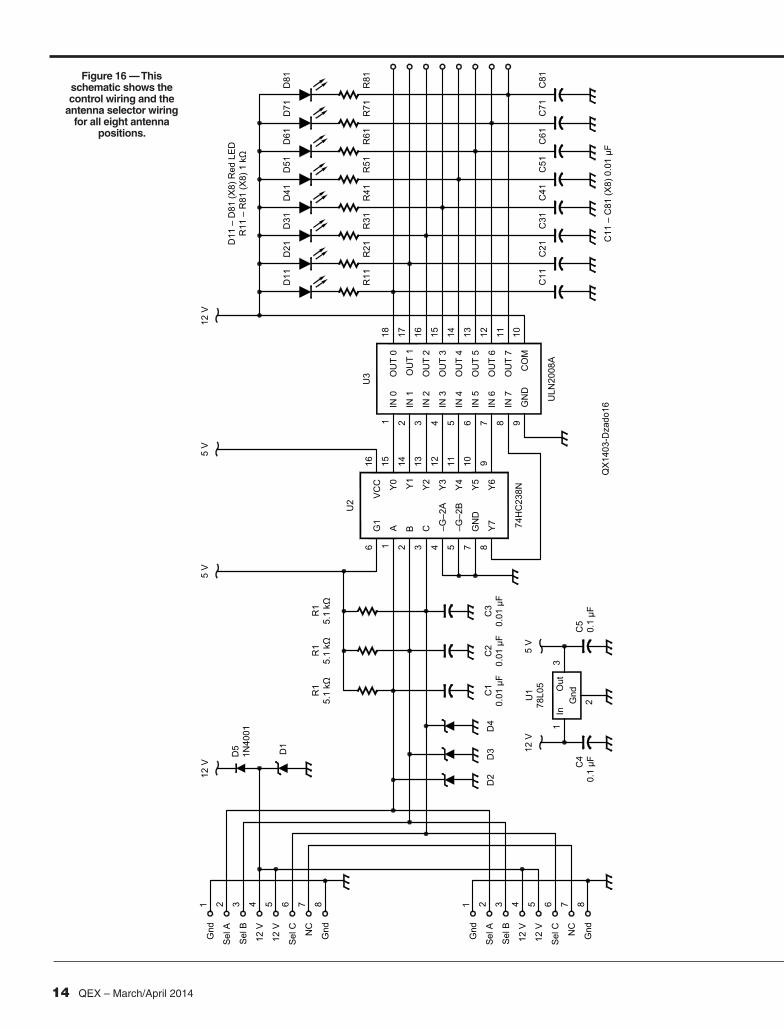
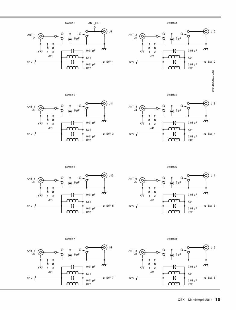
Figure 16 — This schematic shows the control wiring and the
antenna selector wiring for all eight antenna
positions.
QEX – March/April 2014 15
QX
1403
-Dza
do16
ANT_1J1
1 2J11
Switch 1
J9
ANT_OUT
5 pF
0.01 μF
K11
0.01 μFK12
12 V SW_1
ANT_2J2
1 2J21
Switch 2
5 pF
0.01 μF
K21
0.01 μFK22
12 V SW_2
ANT_3J3
1 2J31
Switch 3
5 pF
0.01 μF
K31
0.01 μFK32
12 V SW_3
ANT_4J4
1 2J41
Switch 4
5 pF
0.01 μF
K41
0.01 μFK42
12 V SW_4
ANT_5J5
1 2J51
Switch 5
5 pF
0.01 μF
K51
0.01 μFK52
12 V SW_5
ANT_6J6
1 2J61
Switch 6
5 pF
0.01 μF
K61
0.01 μFK62
12 V SW_6
ANT_7J7
1 2J71
Switch 7
5 pF
0.01 μF
K71
0.01 μFK72
12 V SW_7
ANT_8J8
1 2J81
Switch 8
5 pF
0.01 μF
K81
0.01 μFK82
12 V SW_8
J10
J11 J12
J14J13
15 J16
16 QEX – March/April 2014
QX1403-Dzado17
R1
12 V
C10.1 μF
5 V
C20.1 μF
U178L05
1
2
3OutInGnd
11
22
33
44
55
66
77
88
99
1010
5 V
1X10HDR
P1
R2
R3
R4
R5
R6
R7
R8
R1-R81 kΩ 1 2 3
4
56
78
1010
1111
1212
1313
1414
1515
1616
1717
VCC
7A0
6A1
14
A2
13GC
ED
8
U2
74HC148
E15
GND
16
9A0
A1
A2
14
5 V
C11
C30.1 μF
C12 C13 C14 C15 C16 C17 C18
11
22
33
44
P2
1X4HDR
C41500 pF
F11A
C11-C180.01 μFL1
3.3 μH
D91N4001
QX1403-Dzado18
R101 kΩ
D1RED
R951 Ω
A0
J1
RJ-45
1
5 V
GND2
Sel A3
Sel B4
12 V5
12 V6
Sel C7
NC8
GND
R121 kΩ
D2RED
R1151 Ω
A1
5 V
R141 kΩ
D3RED
R1351 Ω
A22
3
1
5 V
C80.01 μF
12 V
C70.01 μF
C60.01 μF
C50.01 μF
Q32N2222A
2
3
1
Q22N2222A
2
3
1
Q12N2222A
Figure 17 — Here is the antenna selector switch remote control wiring.
Figure 18 — This schematic diagram shows the remote control wiring output to the antenna selector switch.

QEX – March/April 2014 17
Mike Dzado, ACØHB, obtained his Amateur Extra Class License in 2007. Mike has over 35 years combined experience as an Electrical and Software Engineer, which includes CAE/CAD experience. Mike started his career as an Electronic Technician with the USAF and currently is a Senior Systems Engineer for Rockwell Collins Air Transport Large Display Systems. Mike holds an Associate Degree in Meteorological Equipment from the Community College of the Air Force (1978), Bachelor of Science in Electronic Systems Management from Southern Illinois University (1980), Bachelor of Science in
Electrical Engineering from the University of Utah (1984), and a Master of Science in Software Engineering from the National Technological University (1994). Mike’s career experience includes Power Supply Design, Communications Protocol Software Development, Computer Aided Engineering Design and Analysis Tool development, and Software Defined Radio development.
Mike’s other hobbies include weather spotting, and designing and building electronic kits for fellow club members. He is a member of the Cedar Valley Amateur Radio Club (CVARC) and Collins Amateur Radio Club
(CARC) See his website, www.AC0HB.com for some of his current projects.
Notes1Learn more about TinyCAD and download
the program free at: tinycad.en.softonic.com/.
2For more information about the Free PCB program and to download the installation files, go to: www.freepcb.com/.
3You can download the AppCAD design software free from the Avago Technologies website. Go to www.avagotech.com/pages/appcad.