Embed Size (px)
Citation preview
University of Tennessee, Knoxville University of Tennessee, Knoxville
TRACE: Tennessee Research and Creative TRACE: Tennessee Research and Creative
Exchange Exchange
Masters Theses Graduate School
12-2017
An Analog CMOS Particle Filter An Analog CMOS Particle Filter
Trevor Watson University of Tennessee, Knoxville, [email protected]
Follow this and additional works at: https://trace.tennessee.edu/utk_gradthes
Part of the Electrical and Electronics Commons, and the VLSI and Circuits, Embedded and Hardware
Systems Commons
Recommended Citation Recommended Citation Watson, Trevor, "An Analog CMOS Particle Filter. " Master's Thesis, University of Tennessee, 2017. https://trace.tennessee.edu/utk_gradthes/4962
This Thesis is brought to you for free and open access by the Graduate School at TRACE: Tennessee Research and Creative Exchange. It has been accepted for inclusion in Masters Theses by an authorized administrator of TRACE: Tennessee Research and Creative Exchange. For more information, please contact [email protected].
To the Graduate Council:
I am submitting herewith a thesis written by Trevor Watson entitled "An Analog CMOS Particle
Filter." I have examined the final electronic copy of this thesis for form and content and
recommend that it be accepted in partial fulfillment of the requirements for the degree of
Master of Science, with a major in Electrical Engineering.
Jeremy H. Holleman, Major Professor
We have read this thesis and recommend its acceptance:
Benjamin J. Blalock, Garrett S. Rose
Accepted for the Council:
Dixie L. Thompson
Vice Provost and Dean of the Graduate School
(Original signatures are on file with official student records.)
An Analog CMOS Particle Filter
A Thesis Presented for the Master of Science
Degree The University of Tennessee, Knoxville
Trevor Watson December 2017
ii
ACKNOWLEDGEMENTS
Thank you to Dr. Jeremy Holleman for guidance in this project and Ashley Smutnik for proofreading and keeping me on task.

iii
ABSTRACT
Particle filters are used in a variety of image processing and machine learning applications. Their main use in these applications is to gather information about a system of objects, by using partial or noisy observations collected from sensors. These observations are used to associate points of interest in the observations with objects and maintain this association through a series of observations.
In this paper I will investigate the performance of a particle filter implemented in 130nm analog CMOS hardware. The design goal of the particle filter is low-microwatt power consumption. Using analog hardware, rather than digital ASICs or CPUs I hope to achieve this low power consumption.

iv
TABLE OF CONTENTS
Chapter One Introduction and General Information .............................................. 1
1.1 Particle Filter Introduction ........................................................................ 1 1.2 Implementation ........................................................................................ 5
Chapter Two Literature Review ............................................................................ 7
2.1 Particle Filter ............................................................................................ 7 Chapter Three System Description ....................................................................... 9
3.1 Architecture .............................................................................................. 9 3.2 Storage .................................................................................................. 12 3.3 Multiplier ................................................................................................ 19
3.4 Proposal Generator ............................................................................... 20 3.5 Test setup .............................................................................................. 22
Chapter Four Results and Discussion ................................................................. 24 4.1 Sample and Hold ................................................................................... 24 4.2 Multiplier ................................................................................................ 27 4.3 System Test ........................................................................................... 29
Chapter Five Conclusions and Recommendations ............................................. 38 List of References ............................................................................................... 39
Vita ...................................................................................................................... 41

v
LIST OF TABLES
Table 3.1 Sample and Hold Device Sizes ........................................................... 15 Table 3.2 Op-Amp Device Sizes ......................................................................... 18
Table 4.1 Leakage Measurements...................................................................... 25

vi
LIST OF FIGURES
Figure 1.1 10,000 Particle Approximation of Bimodal Gaussian distribution ......... 2 Figure 1.2 (a,b,c) 2-D particle filter. ....................................................................... 3
Figure 3.1 Particle filter block diagram ................................................................ 10 Figure 3.2 Proposal Generator............................................................................ 11 Figure 3.3 Acceptance Ratio Calculator .............................................................. 11 Figure 3.4 Original sample and hold circuit ......................................................... 13 Figure 3.5 Revised sample and hold circuit ........................................................ 14
Figure 3.6 Original sample and hold OP-Amp .................................................... 17 Figure 3.7 Revised Sample and Hold Op-Amp ................................................... 18
Figure 3.8 Multiplier Schematic ........................................................................... 19
Figure 3.9 Proposal Generator............................................................................ 20 Figure 3.10 DAC used in proposal generator ...................................................... 21 Figure 3.11 Transconductor circuit schematic .................................................... 23
Figure 3.12 Transimpedance amplifier ................................................................ 23 Figure 4.1 Feb. 2016 standalone sample and hold cell test with random input ... 25 Figure 4.2 Aug. 16 Sample and hold leakage test. ............................................. 26
Figure 4.3 Simulated results with sinusoidal input .............................................. 26 Figure 4.4 Input DC sweep, Ia/Ic = 3/2 ............................................................... 27
Figure 4.5 Multiplier Step Response, Ia/Ic = 3/2 ................................................. 28 Figure 4.6 Proposal Generator Test (Feb ’16 chip) ............................................. 30 Figure 4.7 Proposal Generator Test (Aug ’16 chip)............................................. 30
Figure 4.8 Sample and Hold Problem (Feb 16) .................................................. 31
Figure 4.9 Revised Sample and Hold Test (Aug 16) ........................................... 32 Figure 4.10 Revise Sample and Hold Step Test (Aug 16) .................................. 32 Figure 4.11 X vs X plot of measured vs expected X values for particles ............. 34
Figure 4.12 Y vs Y plot of measured vs expected Y values for particles ............. 34 Figure 4.13 Simulated object location converging as particles are updated ....... 35
Figure 4.14 Measured object location convergence test. .................................... 35 Figure 4.15 Particle filter series test .................................................................... 37 Figure 4.16 Noise in particle filter test ................................................................. 37

1
CHAPTER ONE
INTRODUCTION AND GENERAL INFORMATION
1.1 Particle Filter Introduction
Particle filters are a series of numerical methods used to estimate the
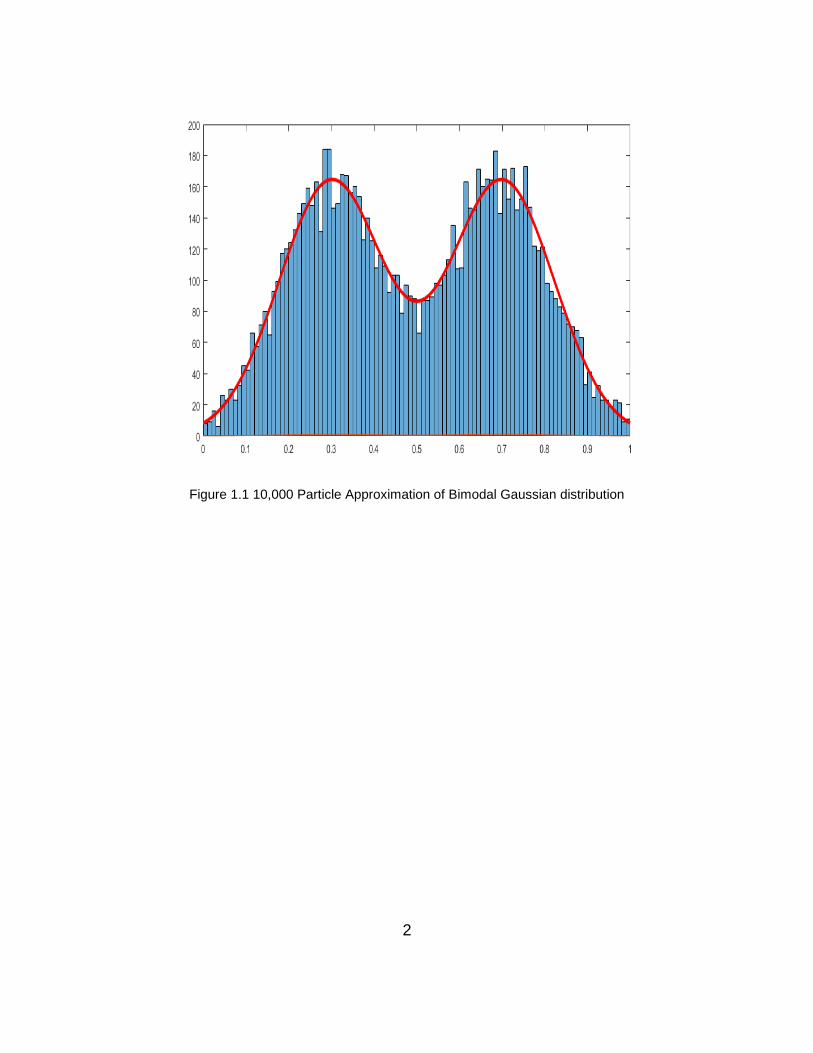
actual state of a system from some partial or incomplete observation of the system. The observations of the system may include noise and other false signals. Determining the state of the system through a series of noisy or incomplete observations is known as the filtering problem. The filtering problem as used for tracking objects in a series of images can be thought of as modeling many guesses about the future location of the object based on its currently assumed location, the probability of the assumed location based on the observed probability distribution, and it’s prior assumed locations. Each guess is represented by a particle, and the distribution of these particles can be viewed as an estimated model for where the object currently is and where it will be in the future. For this system a first-order motion model (velocity) will be used to calculate possible future locations. The estimated future locations can be used to associate detections with objects and maintain this association over a series of observations, even in cases where detections fade in and out or cross over one another. For a given system the location of an object in the system can be described in a continuous probability function over the entire system. For a one dimensional system, such as the location of an object on a line, this can be visualized as a continuous function over the x-axis as shown by the red trace in Figure 1.1, with the y-axis representing the probability of the object at that x location, the higher the peak the more likely the object is at that x-coordinate. If we observe the system over a series of observations and model the anticipated movement of the object as constant velocity along the x-axis we can estimate the objects future location based on its estimated movement along the x-axis.
The particle filter starts by approximating the supplied probability distribution (the observation) with a series of individual points, or particles, as seen in Figure 1.2a These particles represent a guess about the state of the system and are generated using Markov chain Monte Carlo methods to sample points from the supplied probability distribution. Then on the next observation cycle (Figure 1.2b) the probability distribution is updated with a new observation.
2
Figure 1.1 10,000 Particle Approximation of Bimodal Gaussian distribution

3
Figure 1.2 (a,b,c) 2-D particle filter.
Red line is the observation at each time step, the blue points are the particles approximating the
objects probability distribution, and the green trace is the approximated probability distribution
0
0.2
0.4
0.6
0.8
1
0 1 2 3 4 5 6 7 8 9 10
0
0.2
0.4
0.6
0.8
1
0 1 2 3 4 5 6 7 8 9 10
0
0.2
0.4
0.6
0.8
1
0 1 2 3 4 5 6 7 8 9 10
4
The particle filter then generates a new set of particles based on the previous particle locations and the new observation. Over several update and resample iterations the particle filter can converge on the objects estimated location, as shown in Figure 1.2c.
The two main equations describing the prediction and update process are
the Chapman-Kolmogorov equation and Bayes theorem of conditional probability
using the system states 𝑥1:𝑛 and the observed measurements 𝑦1:𝑛. The Chapman-Kolmogorov Equation describes the probability of transition from the
previous state 𝑥𝑛−1 to the current state 𝑥𝑛 through all possible intermediate points, based on all prior measurements 𝑦1:𝑛−1
𝑃(𝑥𝑛|𝑦1:𝑛−1) = ∫ 𝑃(𝑥𝑛|𝑥𝑛−1)𝑃(𝑥𝑛−1|𝑦1:𝑛−1) 𝑑𝑥𝑛−1
Chapman-Kolmogorov Equation
𝑃(𝑥𝑛|𝑦1:𝑛) =𝑃(𝑦𝑛|𝑥𝑛)𝑃(𝑥𝑛|𝑦1:𝑛−1)
𝑃(𝑦𝑛|𝑦1:𝑛−1)
Bayes Theorem
For the particle filter with a finite number of particles the Chapman-Kolmogorov equation becomes the probability of the particle in the current state based on the total probability of all particles in the previous state moving to the location of the particle in the current state. The Chapman-Kolmogorov equation gives the probability of the current state based on all previous states and is recursive. For a first-order Markov process only the previous state is retained and the state transition equation becomes
𝑃(𝑥𝑛) = ∑ 𝑃(𝑥𝑛|𝑥𝑛−1)𝑃(𝑥𝑛−1)
Chapman-Kolmogorov as used in particle filter chip
The system model, 𝑃(𝑥𝑛|𝑥𝑛−1) , describes the expected movement of the particles. The system model for the particle filter chip was chosen to be a first-order, or constant velocity, model. Particles are assumed to move with a constant velocity with a Gaussian noise term added.
After performing the update step, the new observation data 𝑦𝑛 is incorporated into the current state using Bayes theorem. As with the Chapman-Kolmogorov equation this is recursive and is simplified as
𝑃(𝑥𝑛) =𝑃(𝑦𝑛|𝑥𝑛)𝑃(𝑥𝑛)
𝑃(𝑦𝑛)
Bayes Theorem as used in particle filter chip

5
Ideally as the number of particles used to represent the sampling distribution goes to infinity the approximated distribution exactly matches the sampling distribution. Real systems however are limited to a finite number of particles. Analog systems are further limited by the difficulty of analog storage cells. Figure 1.1 shows a representation of a sampling distribution with 10,000 particles The red trace shows the sampling distribution that the particles were drawn from.
1.2 Implementation
The particle filter in this paper was designed to take input data from a
separate correlation filter that identifies areas of interest and generates a probability density function that the particle filter can use as input for the filtering algorithm. The particle filter will then return the location data associated with these areas of interest.
The system described in this paper is designed to be the core of the particle filter algorithm. In its current state it performs the basic particle filtering algorithm for a single frame and an external control system provides the input data to the system and interprets the output data to feed back to the system to operate over multiple frames. The fabricated hardware is used in a hardware-in-the-loop configuration for testing, with a programmable microcontroller used to close the loop. The tested implementation of the particle filter operates on a 32 particle array. During operation a particle, N, from the array is selected as the current particle. The proposal generator randomly generates a new particle to be tested inside the bounding box (x1,y1) (x2,y2). This is then sent to the external test bench to generate the probability associated with the new particle. The acceptance calculator then decides if the new particle should replace the current particle by computing Pnew/Pcurrent and comparing with a random factor. If the acceptance calculator decides to accept the new particle, it is stored in place of the current stored particle. The next particle in the array, N+1 is then selected as the current particle and the process is repeated until a sufficiently accurate particle distribution is generated. For the physical implementation, the signals are represented as currents. Current mode signaling lends itself well to lower voltage applications, as the compliance voltage for current sources becomes a significant fraction of the supply voltage, which can limit the dynamic range of voltage mode signals. Current mode signaling also makes operations such as addition and subtraction easy to implement by simply wiring the outputs of current mirrors together. Multiplication and division were also easier to implement in current mode as such a cell was already available for use. For this system, the multiplier cell was

6
implemented as a subthreshold translinear circuit that can be used for both multiplication and division.

7
CHAPTER TWO
LITERATURE REVIEW
2.1 Particle Filter
Much work has been published on the topic of using particle filters to track
objects. In [1] the authors describe a system for tracking objects based on detector confidence and [2] describes using a particle filtering algorithm in conjunction with a classifier to track single objects. Most of this work focuses on the particle filter algorithm itself or software implementations of the algorithm. Hardware implementations primarily consist of FPGA designs [3] [4].
While using general purpose computers or FPGAs to implement particle
filters is effective, their power draw can be prohibitive in low-power or weight-constrained environments such as drones or other small unmanned aerial vehicles. By implementing the particle filtering algorithm using analog computation blocks instead of digital systems it may be possible to achieve a similar level of performance using significantly less power while still maintaining an acceptable level of accuracy.
The particle filter algorithm description given in [5] was used as the
primary reference for the algorithm. The algorithm consists of two major steps, the prediction step and the update step. The prediction step takes the current distribution of particles and updates them based on the state transition model and current particle location. The probability of the new particle distribution is described by the Chapman-Kolmogorov Equation, which gives the probability of the new particle based on the likelihood of the old particle and the likelihood that the old particle could transition to the new particle. For the object tracking application this would be the equivalent of the probability that an object exists at a given location and the probability that the object moves to the proposed location given its prior motion. Ideally the update step should move the particle distribution in the direction of the object’s assumed motion.
The update step takes the predicted particle distribution and updates it
based on a new observation based on the joint probability of the prediction and observation. The new particle distribution is given by combining the distribution given by the proposed particles from the prediction step and the probability distribution given by the observation. This has the effect that the particles represent objects that are located by the current observations as well as past observations, allowing the system to filter out noise and maintain particle associations with objects.

8
The architecture used by the analog particle filter is most similar to [4], with similar goals for object tracking. The prediction and update steps are combined in a single propose/evaluate step, which reduces the amount of storage required. The analog particle filter is supplied with input data from an upstream correlator that identifies areas of interest and generates a probability distribution for the particle filter to evaluate. Due to the continuous nature of analog systems, the analog particle filter can scale to any desired video resolution and input data. By changing the input correlator, the analog particle filter can be adapted to many machine learning applications.

9
CHAPTER THREE
SYSTEM DESCRIPTION
3.1 Architecture
The particle filter chip (Figure 3.1) consists of 3 main subsystems, the
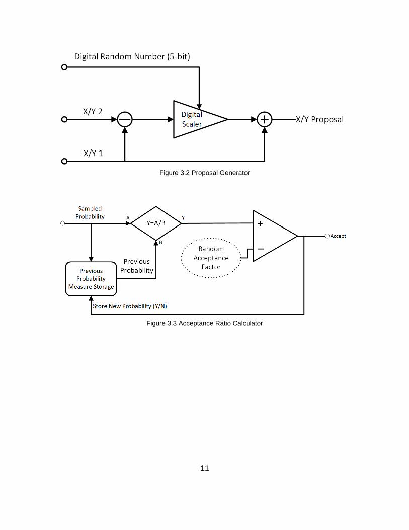
proposal generator, the acceptance calculator, and the particle storage array. The particle storage array consists of 32 particles. In each clock cycle one particle is selected for update. The proposal generator (Figure 3.2) then generates a random X/Y location inside an upper and lower bound to test against the probability density function generated by the correlator. The probability density function consists of a 2D array of likelihood measures. When a proposal is generated, the probability density function returns the likelihood of that proposal based on the current observation. The acceptance ratio calculator (Figure 3.3) then takes this likelihood measurement and computes whether or not to accept the new proposal based on the new likelihood and the previous stored likelihood for the selected particle. If the new particle is selected, then the selected particle is updated with the new position and likelihood values.
The random numbers and probability map as well as the system clocks are generated externally by a PSoC 5 development board. The PSoC is a programmable system on a chip with a 60 MHz ARM core and configurable analog and digital blocks, similar to a FPGA. The PSoC development board is also connected to a PC by a USB-UART connection to read test results.

10
Figure 3.1 Particle filter block diagram
11
Figure 3.2 Proposal Generator
Figure 3.3 Acceptance Ratio Calculator
12
3.2 Storage
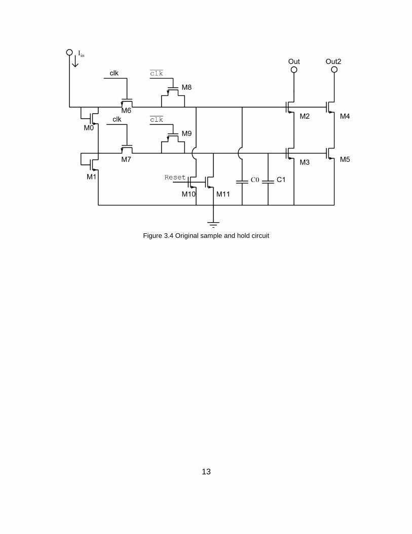
At the core of the particle filter there is an array that stores the location and probability of each particle. With a digital storage system having an array to store each particle location and probability is trivial, thousands of particles can be stored using simple 8-bit microcontrollers. However, with analog hardware the particles must be stored in sample and hold cells. These cells are significantly larger than SRAM or DRAM cells and suffer from leakage effects. Due to the leakage effects a significant amount of time was spent designing a low-leakage high-accuracy current mode sample and hold cell to use for the particle state array. Most published work focuses on voltage mode sample and hold cells for ADC input buffers, which focus primarily speed and accuracy. There are a few examples of sample and hold cells designed primarily for analog memory applications, one of which is given in [6] which only loses 0.025% in 3.3 minutes, however these results were achieved on a 1.2µm process. In the 130nm process the drain-body leakage current is an order of magnitude greater and the sampling capacitor is an order of magnitude smaller than in the example given. Additionally if a voltage mode sample and hold cell were used to drive a current source the exponential Vgs-Id relationship of the subthreshold MOSFET would make the ouput current error increase exponentially with the output voltage drift of the sample and hold cell. The first iteration of the sample and hold cell (Figure 3.4) was a simple cascode current mirror with sample switches and storage capacitors. This iteration was found to lack the accuracy required (5%) due to mismatch in the input and output transistors and insufficient output resistance. The required two capacitors also took up twice the amount of area as a single capacitor design, which became problematic when constructing large storage cell arrays. A revised version of the sample and hold cell had to be fabricated.
The revised sample and hold cell (Figure 3.5) uses a single transistor for both the sample mode and the hold mode as well as a gain-boosted cascode output stage to maximize output resistance. Since only one transistor is used for both input and primary output the effects of mismatch are eliminated for the primary output. The output transistor, M0, as used in this circuit and biased at 60nA drain current has an output resistance of approximately 16M Ω (simulated), thus a 50mV change in output (drain) voltage is sufficient to cause 5% error in the output current. Since the chip is designed to operate from a 1.0-1.2V supply, this could cause a large output current error on the order of 50nA (83% error).
A cascode configuration, as used in the original sample and hold
increases the output resistance by a factor of gmro, which is approximately a
13
Figure 3.4 Original sample and hold circuit

14
Figure 3.5 Revised sample and hold circuit
15
factor of 30 for the conditions described above. This greatly reduces the output current error due to output resistance but adds an additional source of error from the variation of threshold voltage and the complexity of biasing the cascode transistor.
The gain boosted cascode uses an op-amp to control the voltage at the
drain of the output transistor MD0, the output current error is given by
(𝐴𝑜
1+𝐴𝑜𝑉𝑔 + 𝑉𝑜𝑠) 𝑔𝑑𝑠𝑀𝐷0
. Since the open loop gain of the op amp is large
(Approximately 800 for the op-amp used) then the output current error is dominated by Vosgds. To meet the 5% output error requirement the offset error of the op amp should be less than than 50mV, which is easily achievable. The op-amp used in the sample and hold cell has an average input referred offset of 8.3mV based on Monte-Carlo simulations. The gain boosted cascode configuration is self-biasing, setting the drain voltage of the output transistor based on its gate voltage. This greatly reduces the effect of the transistor output resistance.
The sample and hold cell also includes a second output transistor for a
secondary output. In the particle filter system sample and hold cells are used to store both the particle location and the probability weight associated with each particle. The second output is only used in the particle location array to compute the average of the particles in the location array. While the secondary output is affected by inaccuracies caused by transistor mismatch, when the average of several outputs is taken the average output error becomes the average error of all the cells, reducing the effects of a single bad cell. Device sizes for the sample and hold cell are listed in Table 3.1.
Table 3.1 Sample and Hold Device Sizes
Device Type W/L Value
M0, M1 nfet 2μ/2μ
M2-M10 nfet 160n/120n
M11 Hi-Vt nfet 320n/120n, nf=2
M12 Hi-Vt nfet 500n/500n
M13 Hi-Vt nfet 160n/120n
C0 MimCap 17.5μ/8.75μ ~322 fF
MD0,MD1 Nfet 1μ/2μ
16
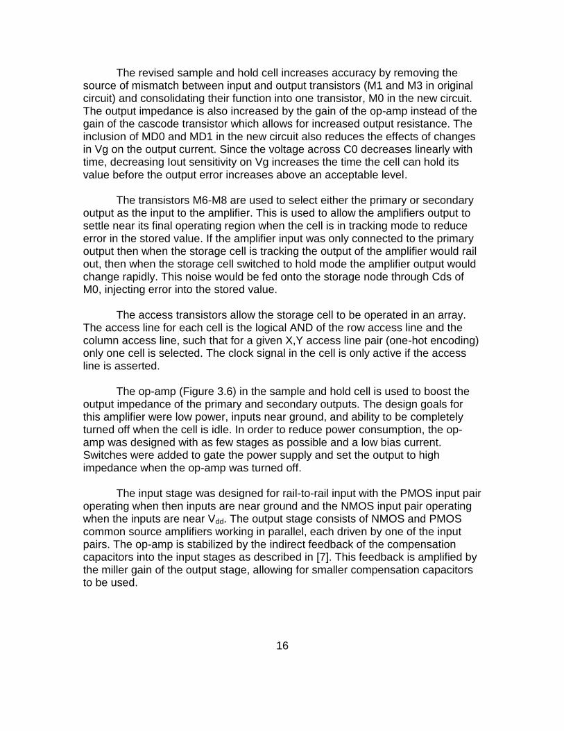
The revised sample and hold cell increases accuracy by removing the source of mismatch between input and output transistors (M1 and M3 in original circuit) and consolidating their function into one transistor, M0 in the new circuit. The output impedance is also increased by the gain of the op-amp instead of the gain of the cascode transistor which allows for increased output resistance. The inclusion of MD0 and MD1 in the new circuit also reduces the effects of changes in Vg on the output current. Since the voltage across C0 decreases linearly with time, decreasing Iout sensitivity on Vg increases the time the cell can hold its value before the output error increases above an acceptable level. The transistors M6-M8 are used to select either the primary or secondary output as the input to the amplifier. This is used to allow the amplifiers output to settle near its final operating region when the cell is in tracking mode to reduce error in the stored value. If the amplifier input was only connected to the primary output then when the storage cell is tracking the output of the amplifier would rail out, then when the storage cell switched to hold mode the amplifier output would change rapidly. This noise would be fed onto the storage node through Cds of M0, injecting error into the stored value. The access transistors allow the storage cell to be operated in an array. The access line for each cell is the logical AND of the row access line and the column access line, such that for a given X,Y access line pair (one-hot encoding) only one cell is selected. The clock signal in the cell is only active if the access line is asserted. The op-amp (Figure 3.6) in the sample and hold cell is used to boost the output impedance of the primary and secondary outputs. The design goals for this amplifier were low power, inputs near ground, and ability to be completely turned off when the cell is idle. In order to reduce power consumption, the op-amp was designed with as few stages as possible and a low bias current. Switches were added to gate the power supply and set the output to high impedance when the op-amp was turned off.
The input stage was designed for rail-to-rail input with the PMOS input pair operating when then inputs are near ground and the NMOS input pair operating when the inputs are near Vdd. The output stage consists of NMOS and PMOS common source amplifiers working in parallel, each driven by one of the input pairs. The op-amp is stabilized by the indirect feedback of the compensation capacitors into the input stages as described in [7]. This feedback is amplified by the miller gain of the output stage, allowing for smaller compensation capacitors to be used.
17
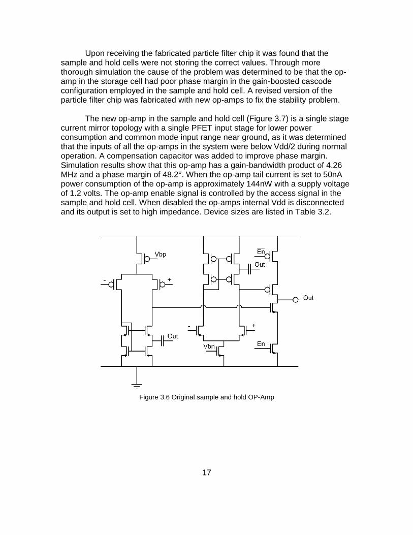
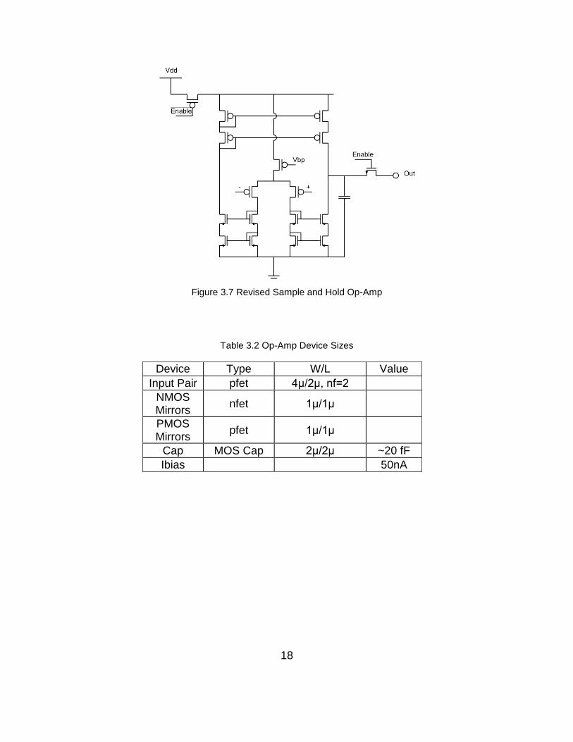
Upon receiving the fabricated particle filter chip it was found that the sample and hold cells were not storing the correct values. Through more thorough simulation the cause of the problem was determined to be that the op-amp in the storage cell had poor phase margin in the gain-boosted cascode configuration employed in the sample and hold cell. A revised version of the particle filter chip was fabricated with new op-amps to fix the stability problem. The new op-amp in the sample and hold cell (Figure 3.7) is a single stage current mirror topology with a single PFET input stage for lower power consumption and common mode input range near ground, as it was determined that the inputs of all the op-amps in the system were below Vdd/2 during normal operation. A compensation capacitor was added to improve phase margin. Simulation results show that this op-amp has a gain-bandwidth product of 4.26 MHz and a phase margin of 48.2°. When the op-amp tail current is set to 50nA power consumption of the op-amp is approximately 144nW with a supply voltage of 1.2 volts. The op-amp enable signal is controlled by the access signal in the sample and hold cell. When disabled the op-amps internal Vdd is disconnected and its output is set to high impedance. Device sizes are listed in Table 3.2.
Figure 3.6 Original sample and hold OP-Amp
18
Figure 3.7 Revised Sample and Hold Op-Amp
Table 3.2 Op-Amp Device Sizes
Device Type W/L Value
Input Pair pfet 4μ/2μ, nf=2
NMOS Mirrors
nfet 1μ/1μ
PMOS Mirrors
pfet 1μ/1μ
Cap MOS Cap 2μ/2μ ~20 fF
Ibias 50nA

19
3.3 Multiplier
Mathematical operations in the particle filter consist of the 4 primary
arithmetic operations, addition, subtraction, multiplication, and division. Since signals in the chip are represented as currents, addition and subtraction is achieved by tying two or more currents together, according to Kirchoff’s current law. Multiplication and division however are more complicated and require active devices. The most common way to implement multiplication and division in analog hardware is to utilize the translinear principle of a PN junction. In the 8RF process the diodes are large and not very good for low-power signal processing so instead MOSFETs operated in the subthreshold region were used. [8]
In the multiplier circuit used in this chip (Figure 3.8) M1-M4 form a
translinear loop. M1, M2 and M3 are used to take the logarithm of 𝐼𝑎, 𝐼𝑏, and 𝐼𝑐, respectively. The voltage at the gate of M4 is given by
𝑙𝑜𝑔(𝐼𝑎) + 𝑙𝑜𝑔(𝐼𝑏) – 𝑙𝑜𝑔(𝐼𝑐), or 𝑉𝑔𝑠2 + 𝑉𝑔𝑠1
– 𝑉𝑔𝑠3. The drain current of M4 is then
the antilog of the gate voltage of M4. Thus the output current corresponds to
𝐼𝑎 ∗ 𝐼𝑏/𝐼𝑐. Transistors M5 and M6 are used to minimize the effects of 𝐺𝑑𝑠 of M2 and M4, respectively.
Figure 3.8 Multiplier Schematic

20
3.4 Proposal Generator
The Proposal generator (Figure 3.9) consists of a 6-bit DAC to supply the
scaling factor and two boundary signals to define the upper limit (𝑋2) and lower limit (𝑋1) of the proposal generator. The purpose of these signals is to limit the particle proposals to an area of interest or control the dynamic range of the system.
The proposal generator operates by taking the difference of the upper and
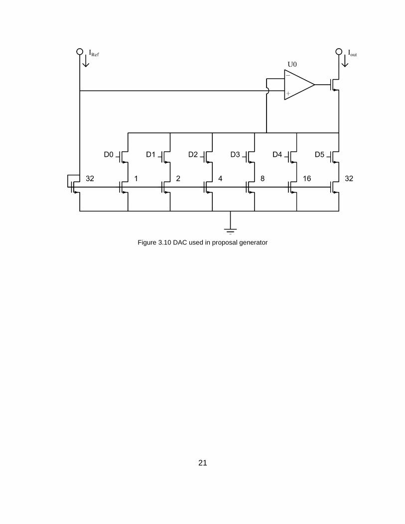
lower bound signals and scaling it by the 6-bit digital input D using the DAC. The output signal from the DAC is added back to the lower bound signal so that the output is greater than the lower bound and less than the upper bound. The DAC (Figure 3.10) is a series of scaled current mirrors used to create power of two fractions of the reference current. By turning on select portions of these scaled current mirrors any fraction of the reference current can be produced. This approach was used instead of a multiplier due to its simplicity and accuracy over large dynamic ranges compared to the multiplier used in this system. It also allows for direct digital inputs, which makes suppling inputs from off chip systems much easier.
Figure 3.9 Proposal Generator
21
Figure 3.10 DAC used in proposal generator
22
3.5 Test setup
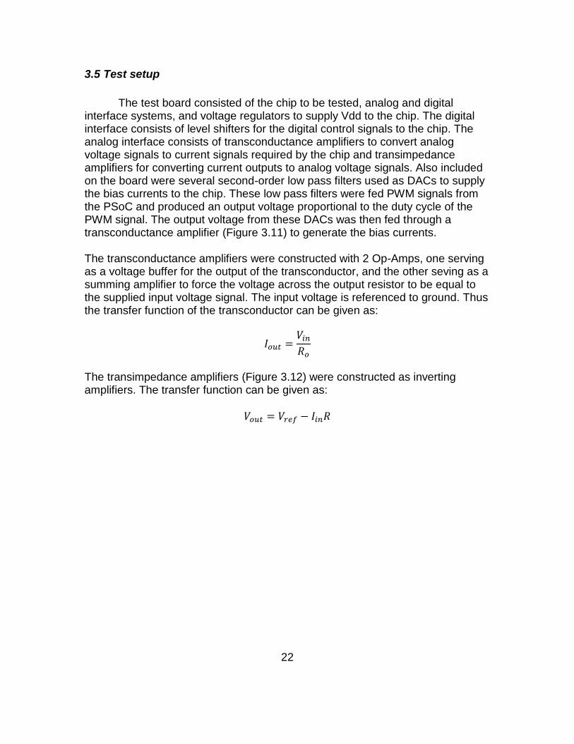
The test board consisted of the chip to be tested, analog and digital interface systems, and voltage regulators to supply Vdd to the chip. The digital interface consists of level shifters for the digital control signals to the chip. The analog interface consists of transconductance amplifiers to convert analog voltage signals to current signals required by the chip and transimpedance amplifiers for converting current outputs to analog voltage signals. Also included on the board were several second-order low pass filters used as DACs to supply the bias currents to the chip. These low pass filters were fed PWM signals from the PSoC and produced an output voltage proportional to the duty cycle of the PWM signal. The output voltage from these DACs was then fed through a transconductance amplifier (Figure 3.11) to generate the bias currents. The transconductance amplifiers were constructed with 2 Op-Amps, one serving as a voltage buffer for the output of the transconductor, and the other seving as a summing amplifier to force the voltage across the output resistor to be equal to the supplied input voltage signal. The input voltage is referenced to ground. Thus the transfer function of the transconductor can be given as:
𝐼𝑜𝑢𝑡 =𝑉𝑖𝑛
𝑅𝑜
The transimpedance amplifiers (Figure 3.12) were constructed as inverting amplifiers. The transfer function can be given as:
𝑉𝑜𝑢𝑡 = 𝑉𝑟𝑒𝑓 − 𝐼𝑖𝑛𝑅

23
Figure 3.11 Transconductor circuit schematic
Figure 3.12 Transimpedance amplifier

24
CHAPTER FOUR
RESULTS AND DISCUSSION
Simulated results show that the particle filter chip is capable of approximating the supplied probability map with the particle locations. The tested chip was unable to do this, as the sample and hold cells in the particle array were not able to store correct values. It was determined that the gain-boosted cascode configuration in the sample and hold cell was unstable, causing the cell to store a random and incorrect value. Since the output of the chip is directly read from sample and hold cells, the chip was unable to produce accurate output. Testing did show the proposal generator working correctly, and the acceptance ratio calculator did appear to work.
4.1 Sample and Hold
As documented in section 3.2 the sample and hold cells from the Feb.
2016 chip do not function as intended in the particle array. The standalone sample and hold cell taped out in Feb. 2016 did provide some useful results however. Presented here are the test results from Feb. 2016 and the simulation results for the latest revision of the sample and hold cell.
Figure 4.1 shows the test results from the standalone sample and hold
cell. The blue trace is the input signal provided to the cell and the yellow trace is the output of the cell. The input signal is a pseudorandom stepped sequence passed through a low pass filter. The purple trace is the sample signal and the green trace is reset. This test shows that the cell is capable of storing a value for at least 600µs.
Figure 4.3 shows the simulation results from sampling a 29.1kHz sine
wave at 20kHz. Sampling time was 5µs. Measured sampling error was approximately 2.0% for this test. When sampling a 60nA DC input signal the sampling error was approximately 0.3% The DC signal test more accurately represents how the sample and hold cell is used in the particle filter.
For a 200 point monte carlo simulation with a 100nA input signal the mean
sampling error was 0.54% with a 0.39% standard deviation. The secondary output had a mean output error of 6.1% with a 4.9% standard deviation. The output was measured 5μs after the end of the sample phase to minimize the effects of leakage and clock noise on the output signal.

25
Leakage was tested by sampling a 100nA input signal and holding for 10ms. In a 20 run Monte Carlo simulation the average leakage over 10ms was 2.5% with a standard deviation of 1.8%. The leakage over 16.7ms was 4.1% with a standard deviation of 2.8%. Measured results from the leakage test is shown in Figure 4.2. Test results for both simulation and measurement are shown in Table 4.1.
Table 4.1 Leakage Measurements
Time Simulated Leakage Measured Leakage
10 ms 2.5% 7.5%
16.7 ms 4.1% 10.5%
Figure 4.1 Feb. 2016 standalone sample and hold cell test with random input

26
Figure 4.2 Aug. 16 Sample and hold leakage test.
Blue trace is the stored value of the cell and yellow trace is the storage clock.
Figure 4.3 Simulated results with sinusoidal input
27
4.2 Multiplier
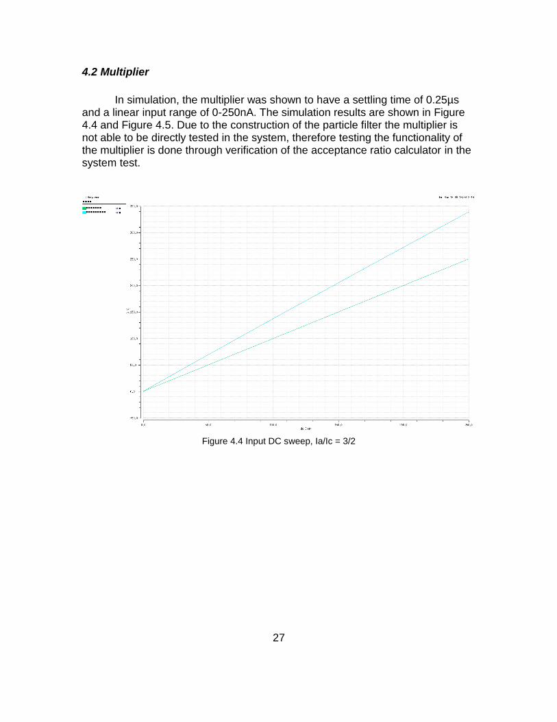
In simulation, the multiplier was shown to have a settling time of 0.25µs
and a linear input range of 0-250nA. The simulation results are shown in Figure 4.4 and Figure 4.5. Due to the construction of the particle filter the multiplier is not able to be directly tested in the system, therefore testing the functionality of the multiplier is done through verification of the acceptance ratio calculator in the system test.
Figure 4.4 Input DC sweep, Ia/Ic = 3/2
28
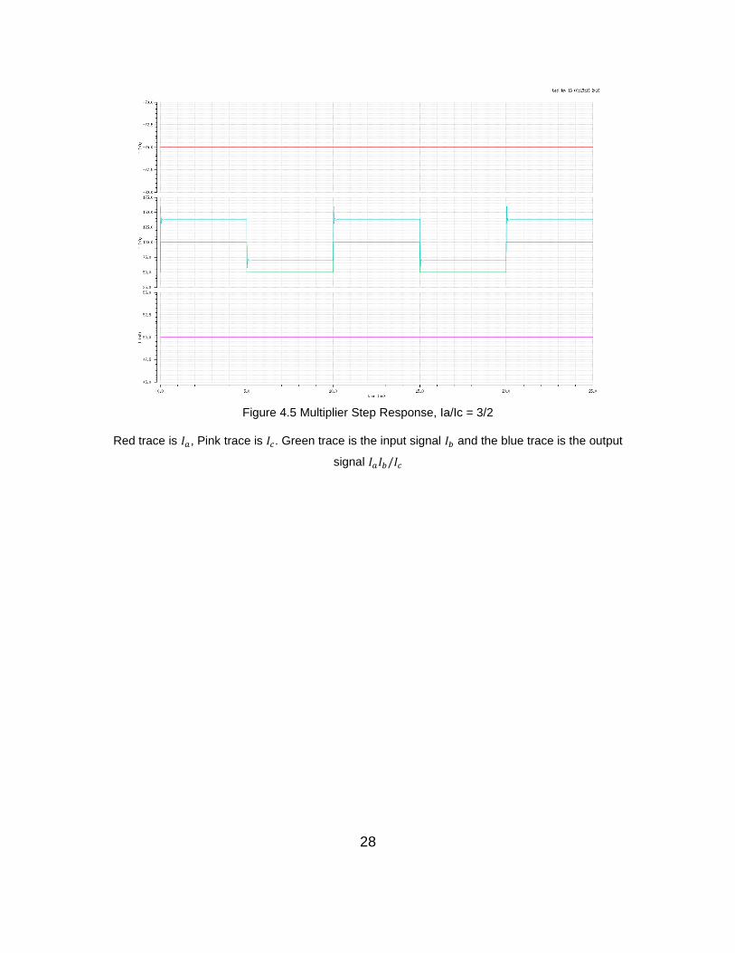
Figure 4.5 Multiplier Step Response, Ia/Ic = 3/2
Red trace is 𝐼𝑎, Pink trace is 𝐼𝑐. Green trace is the input signal 𝐼𝑏 and the blue trace is the output
signal 𝐼𝑎𝐼𝑏/𝐼𝑐

29
4.3 System Test
Testing the system started with verifying the capability of the PSoC to
drive input signals and read output signal from the test board. After basic functionality tests were completed the first component tested was the proposal generator. The proposal generator was tested by setting the upper and lower bounds of the proposal generator and sweeping the 5-bit input from 0 to 63. The PSoC is also used to supply a probability value for that particle based on the proposed location. A Gaussian probability distribution centered near the middle of the upper and lower bounds was used for this test. The expected result was a linear sweep of the particle location and a Gaussian trace for the probability signal.
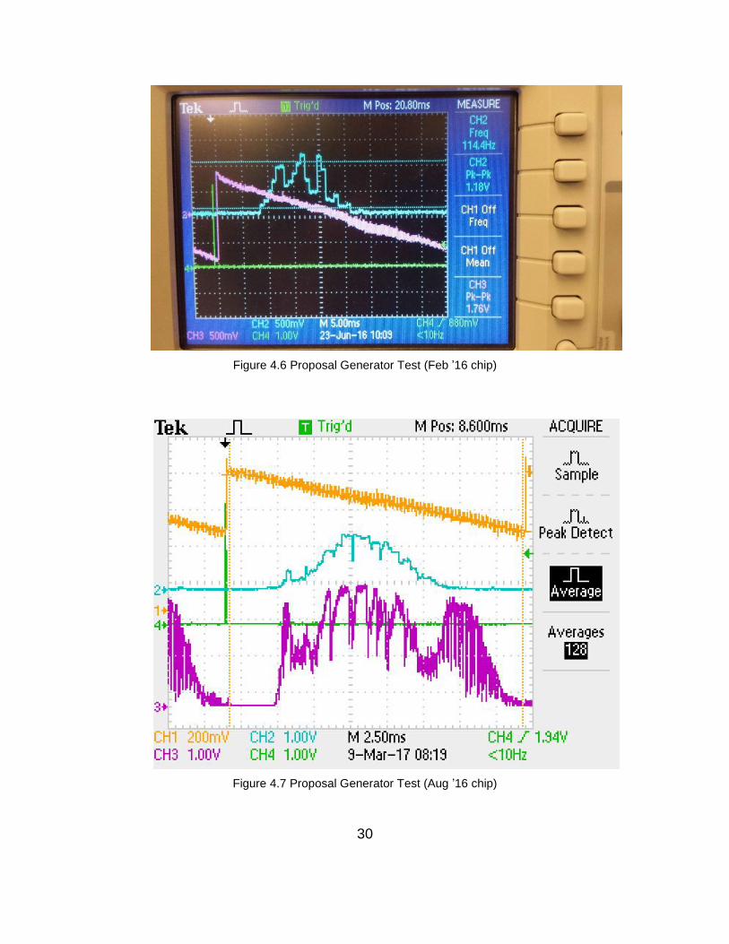
Figure 4.6 and Figure 4.7 show the testing of the proposal generator and PSoC proposal probability loop. In Figure 4.6 (Feb 16) the purple trace is the proposed particle location and the blue trace is the particle probability computed by the PSoC. The blue trace resembles a Gaussian “bump” but is noisy. The source of this noise was not located but is most likely due to arithmetic precision or errors on the PSoC (16-bit) or noise in the ADC. The proposal generator test was also ran with random input values as seen in Error! Reference source not ound..
Figure 4.7 (Aug 16) shows the proposal generator test with the revised
particle filter chip. The orange trace is the particle location and the blue trace is the particle probability. Additionally included in this test is the average number of particles accepted for the corresponding proposal, represented by the purple trace. These results were the average over 128 runs to get a better representation of the particle acceptance distribution. The proposal generator shows slightly better linearity in the revised particle filter.
30
Figure 4.6 Proposal Generator Test (Feb ’16 chip)
Figure 4.7 Proposal Generator Test (Aug ’16 chip)
31
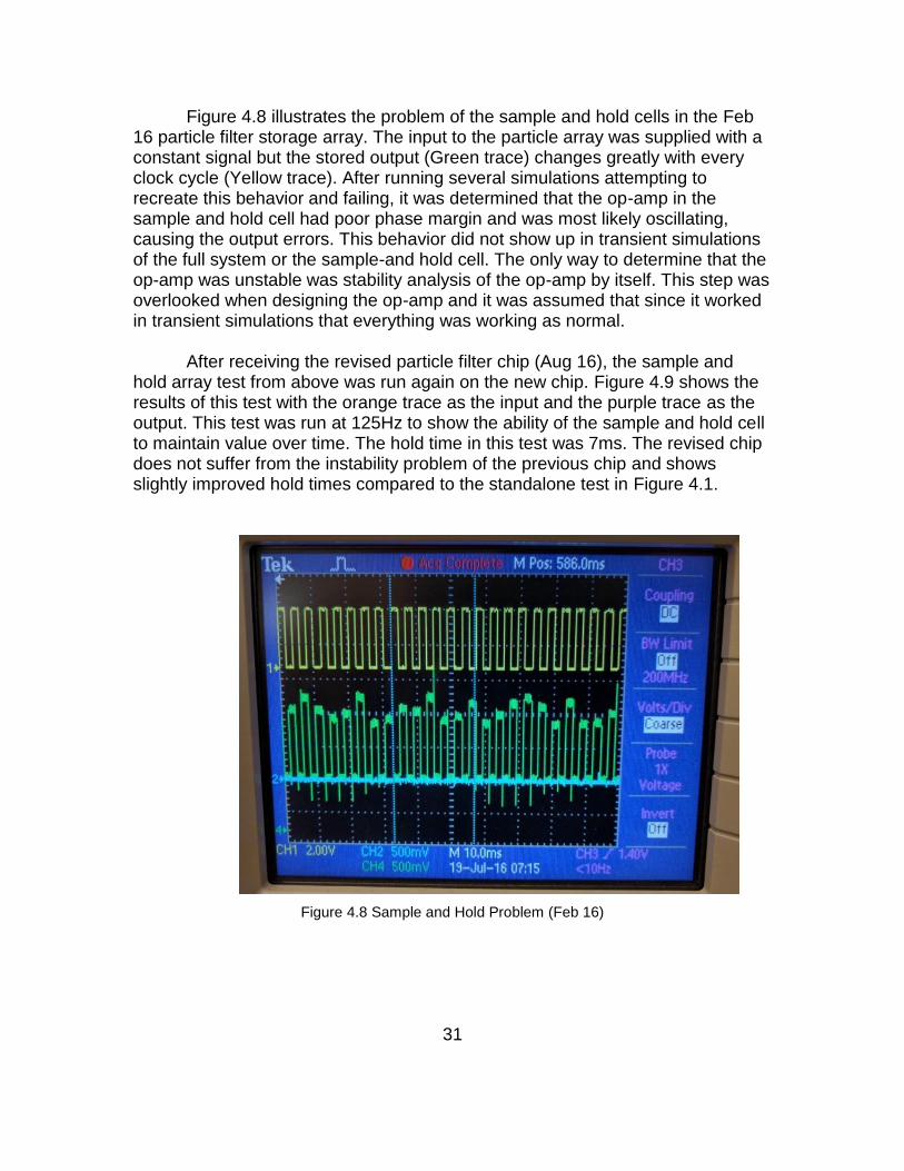
Figure 4.8 illustrates the problem of the sample and hold cells in the Feb 16 particle filter storage array. The input to the particle array was supplied with a constant signal but the stored output (Green trace) changes greatly with every clock cycle (Yellow trace). After running several simulations attempting to recreate this behavior and failing, it was determined that the op-amp in the sample and hold cell had poor phase margin and was most likely oscillating, causing the output errors. This behavior did not show up in transient simulations of the full system or the sample-and hold cell. The only way to determine that the op-amp was unstable was stability analysis of the op-amp by itself. This step was overlooked when designing the op-amp and it was assumed that since it worked in transient simulations that everything was working as normal.
After receiving the revised particle filter chip (Aug 16), the sample and
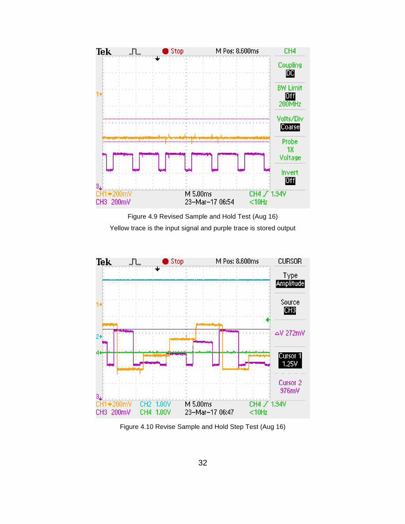
hold array test from above was run again on the new chip. Figure 4.9 shows the results of this test with the orange trace as the input and the purple trace as the output. This test was run at 125Hz to show the ability of the sample and hold cell to maintain value over time. The hold time in this test was 7ms. The revised chip does not suffer from the instability problem of the previous chip and shows slightly improved hold times compared to the standalone test in Figure 4.1.
Figure 4.8 Sample and Hold Problem (Feb 16)
32
Figure 4.9 Revised Sample and Hold Test (Aug 16)
Yellow trace is the input signal and purple trace is stored output
Figure 4.10 Revise Sample and Hold Step Test (Aug 16)
33
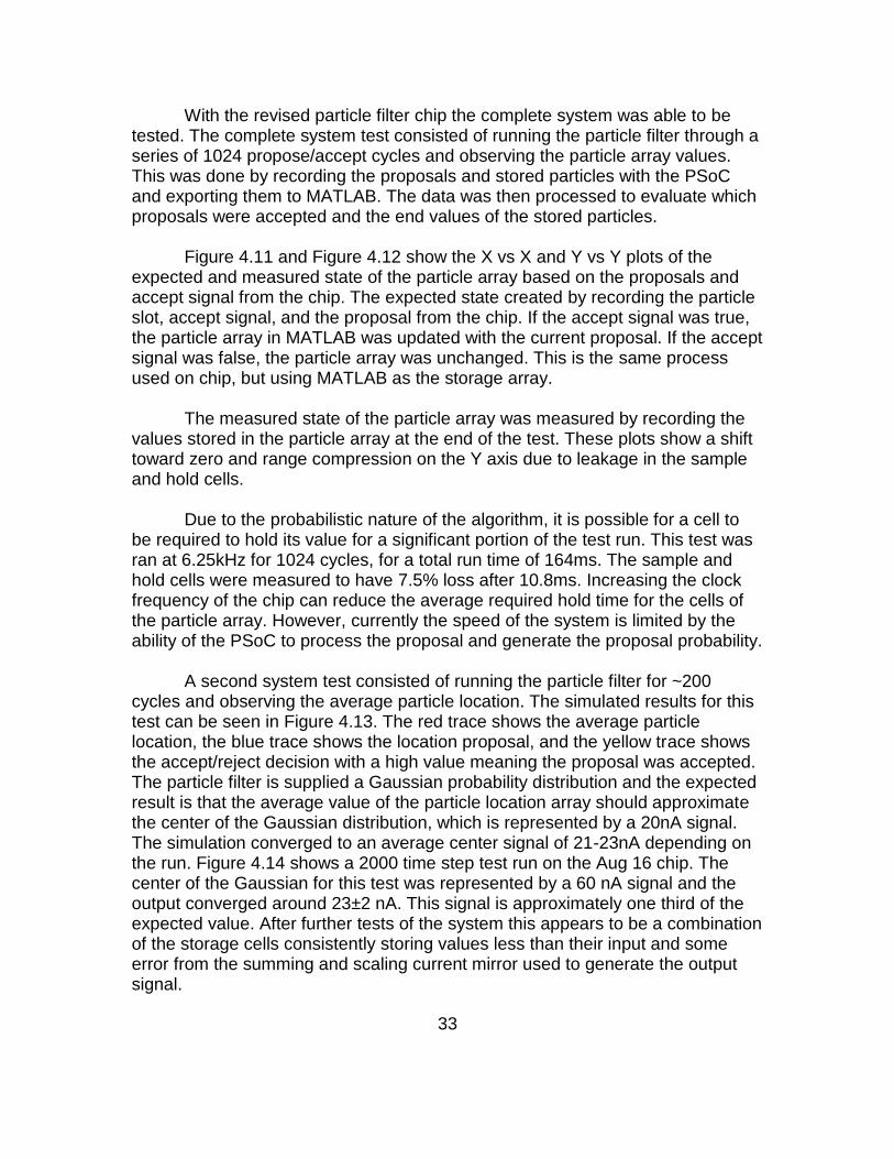
With the revised particle filter chip the complete system was able to be tested. The complete system test consisted of running the particle filter through a series of 1024 propose/accept cycles and observing the particle array values. This was done by recording the proposals and stored particles with the PSoC and exporting them to MATLAB. The data was then processed to evaluate which proposals were accepted and the end values of the stored particles. Figure 4.11 and Figure 4.12 show the X vs X and Y vs Y plots of the expected and measured state of the particle array based on the proposals and accept signal from the chip. The expected state created by recording the particle slot, accept signal, and the proposal from the chip. If the accept signal was true, the particle array in MATLAB was updated with the current proposal. If the accept signal was false, the particle array was unchanged. This is the same process used on chip, but using MATLAB as the storage array. The measured state of the particle array was measured by recording the values stored in the particle array at the end of the test. These plots show a shift toward zero and range compression on the Y axis due to leakage in the sample and hold cells. Due to the probabilistic nature of the algorithm, it is possible for a cell to be required to hold its value for a significant portion of the test run. This test was ran at 6.25kHz for 1024 cycles, for a total run time of 164ms. The sample and hold cells were measured to have 7.5% loss after 10.8ms. Increasing the clock frequency of the chip can reduce the average required hold time for the cells of the particle array. However, currently the speed of the system is limited by the ability of the PSoC to process the proposal and generate the proposal probability. A second system test consisted of running the particle filter for ~200 cycles and observing the average particle location. The simulated results for this test can be seen in Figure 4.13. The red trace shows the average particle location, the blue trace shows the location proposal, and the yellow trace shows the accept/reject decision with a high value meaning the proposal was accepted. The particle filter is supplied a Gaussian probability distribution and the expected result is that the average value of the particle location array should approximate the center of the Gaussian distribution, which is represented by a 20nA signal. The simulation converged to an average center signal of 21-23nA depending on the run. Figure 4.14 shows a 2000 time step test run on the Aug 16 chip. The center of the Gaussian for this test was represented by a 60 nA signal and the output converged around 23±2 nA. This signal is approximately one third of the expected value. After further tests of the system this appears to be a combination of the storage cells consistently storing values less than their input and some error from the summing and scaling current mirror used to generate the output signal.

34
Figure 4.11 X vs X plot of measured vs expected X values for particles
Figure 4.12 Y vs Y plot of measured vs expected Y values for particles
0
10
20
30
40
50
0 10 20 30 40 50
Mea
sure
d X
Co
ord
inat
e
Expected X Coordinate
X vs X
0
10
20
30
40
50
0 10 20 30 40 50
Mea
sure
d Y
Co
ord
inat
e
Expected Y Coordinate
Y vs Y

35
Figure 4.13 Simulated object location converging as particles are updated
Figure 4.14 Measured object location convergence test.
Blue trace is raw output, orange trace is a moving window average of the output.
36
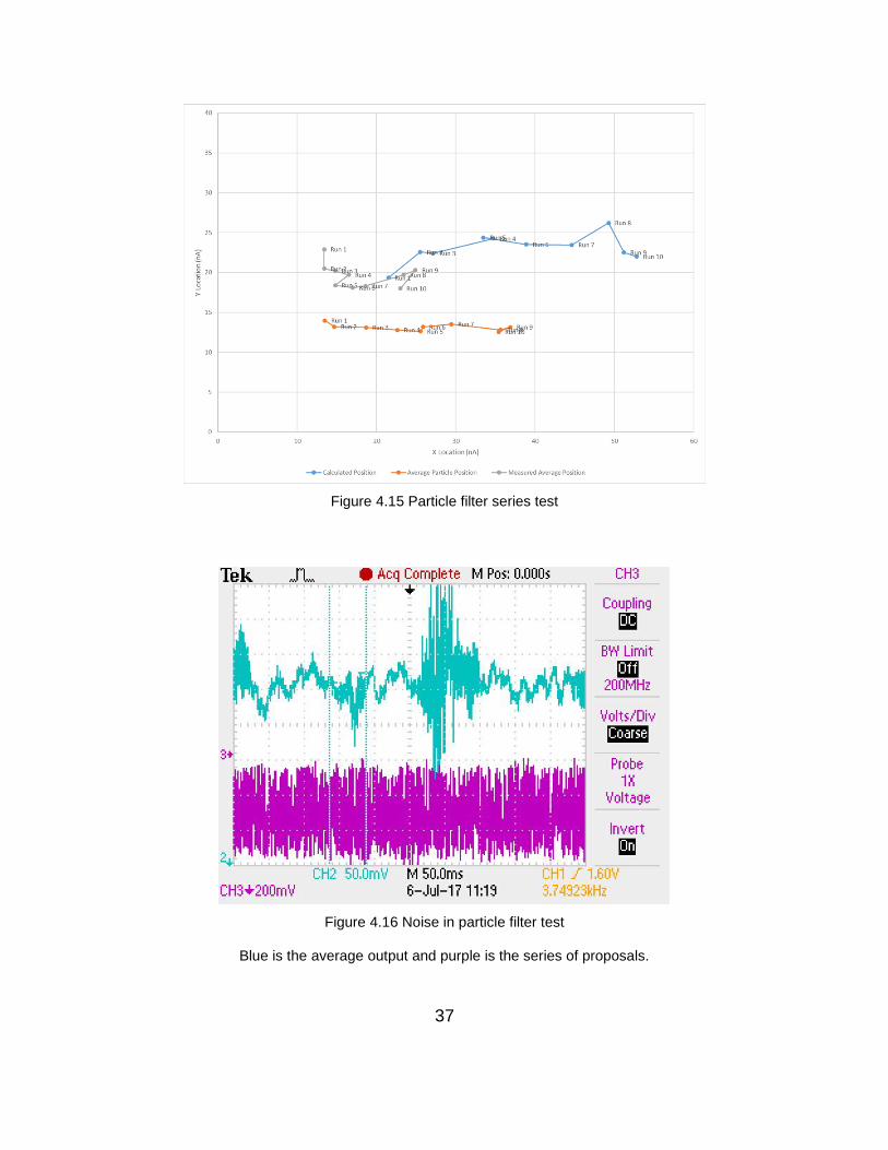
The particle filter chip was also tested by running a series of 10 runs with a moving input Gaussian distribution. Each run consisted of 2000 timesteps and produced a 32-particle cloud and an average location of the input distribution. The input Gaussian was moved from a center location of (15,30) to (65,30) and the average output for each run was measured 3 times, once by averaging the accepted proposals for each particle, once by measuring the average stored values of the particles at the end of the run, and once by directly measuring the average output of the chip. The results of this test is shown in Figure 4.15. The calculated position (Measurement 1) is the most accurate, however it entirely bypasses on chip storage and forces most of the algorithm to be performed off chip.
The average of the measured particle position (Measurement 2) uses the stored particle position and computes the average. This uses the on-chip storage but still requires off chip computation. The measured average position (Measurement 3) uses the full system and should be approximately identical to measurement 2, however there appears to be significant error. This error appears to be caused by noise in the output, as there is occasionally a large difference in measured output between two time steps during a run, when the maximum change between two time steps should only be approximately 1/32 of the average value. Even without the noise, the average output magnitude is lower than expected due to the lower than expected stored values shown in measurement 2. The noise problem is shown in Figure 4.16 where the average output (Blue trace) is expected to be the average of the series of proposals (Purple trace). However the average output contains a large unexpected burst of noise.
Power consumption of the chip while testing was measured at 32μW with the storage array outputs turned on and 2.2μW with outputs turned off. The designed operation of the particle filter is to have the storage array outputs off while processing and then turning them on only to read the output, reducing the average power consumption closer to the output-off result.
37
Figure 4.15 Particle filter series test
Figure 4.16 Noise in particle filter test
Blue is the average output and purple is the series of proposals.
38
CHAPTER FIVE
CONCLUSIONS AND RECOMMENDATIONS
Results showed that the particle filter was able to approximate a probability distribution using a series of 32 particles and store the particles in an array. Simulated results showed that the particle filter could accurately represent a probability distribution and compute an average location, but measured results showed significant error. Signal integrity issues with the test setup limited the accuracy of test results but test results did show that the fabricated chip was able to function. An improved test board with an integrated PSoC microcontroller or on-board ADC would improve test results. Maximum power consumption was 32μW which is significantly less than most microprocessor or FPGA circuits After testing and analysis of the particle filtering algorithm it was determined that the method described in this paper may not take advantage of the capabilities of analog ASICs. While the approach described in this paper would be appropriate for a sequential digital implementation, for analog systems a massively parallel approach would be much more fitting. An improved version of this system could consist of an array of uniform computation and storage blocks that stores a guess about the probability map based on the motion of objects. Then for every new frame the stored guess is updated to more accurately reflect the new information. This method would result in a faster and more scalable system, each update would only take one clock cycle and resolution can be increased by adding more computation/storage blocks. This design may increase power consumption due to increased active units however.
39
LIST OF REFERENCES
40
[1] M. D. Breitenstein, F. Reichlin, B. Leibe, E. Koller-Meier and L. Van Gool, "Robust tracking-by-detection using a detector confidence particle filter," in IEEE 12th International Conference on Computer Vision, Kyoto, 2009.
[2] S. Avidan, "Ensemble Tracking," IEEE Transactions on Pattern Analysis and Machine Intelligence, pp. vol. 29, no. 2, pp. 261-271, 2007.
[3] J. U. Cho, S. H. Jin, X. D. Pham, J. W. Jeon, J. E. Byun and H. Kang, "A Real-Time Object Tracking System Using a Particle Filter," IEEE/RSJ International Conference on Intelligent Robots and Systems, pp. 2822-2827, 2006.
[4] J. Alarcon, R. Salvador, F. Moreno, P. Cobos and I. Lopez, "A new Real-Time Hardware Architecture for Road Line Tracking Using a Particle Filter," IECON 2006 - 32nd Annual Conference on IEEE Industrial Electronics, pp. 736-741, 2006.
[5] M. S. Arulampalam, S. Maskell, N. Gordon and T. Clapp, "A tutorial on particle filters for online nonlinear/non-Gaussian Bayesian tracking," IEEE Transactions on Signal Processing, vol. 50, no. 2, pp. 174-178, 2002.
[6] M. O'Halloran and R. Sarpeshkar, "A 10-nW 12-bit Accurate Analog Storage Cell With 10-aA Leakage," IEEE Journal of Solid-State Circuits, vol. 39, no. 11, pp. 1985-1996, 2004.
[7] V. Saxena and R. J. Baker, "Indirect Feedback Compensation of CMOS op-amps," in 2006 IEEE Workshop on Microelectronics and Electron Devices, Boise, 2006.
[8] A. Andreou and K. Boahen, "Translinear circuits in subthreshold MOS," Analog Integrated Circuits Signal Processing, pp. Vol. 9, pp. 141-166, 1996.
41
VITA
Trevor Watson graduated high school in 2010. He then attended Roane State Community College and was awarded an Associates in Science degree in 2012. He then transferred to the University of Tennessee where he graduated in December 2014 with a Bachelors of Science in Electrical Engineering.