Embed Size (px)
Citation preview
UNIVERSIDAD DE SEVILLADepartamento de Electrónica y Electromagnetismo
UNIVERSIDAD DE LA REPÚBLICAInstituto de Ingeniería Eléctrica
An All-Inversion-Regiongm/ID Based Design Methodology
for Radiofrequency Blocks in CMOSNanometer Technologies
Memoria presentada por
RAFAELLA FIORELLI MARTEGANI
para optar al grado de Doctora
por la Universidad de Sevilla y la Universidad de la República
Octubre, 2011


An All-Inversion-Regiongm/ID Based Design Methodology
for Radiofrequency Blocks in CMOSNanometer Technologies
Memoria presentada por
RAFAELLA FIORELLI MARTEGANI
para optar al grado de Doctora
por la Universidad de Sevilla y la Universidad de la República
Octubre, 2011
Dirigida por
Dr. Eduardo Peralías Macías Dr. Fernando Silveira Noguerol
Científico Titular del CSIC Profesor Titular - Universidad
IMSE-CNM, España de la República, Uruguay
Tutores :
Prof. Adoración Rueda Rueda
Catedrática de la Universidad de Sevilla, España
Prof. Fernando Silveira Noguerol
Profesor Titular -Universidad de la República, Uruguay
Departamento de Electrónica y ElectromagnetismoUniversidad de Sevilla
Instituto de Ingeniería EléctricaUniversidad de la República


A mi familia y a Juan.


sta tesis fue realizada en Régimen de Cotutela entre la Universidad de Sevilla, España y la Universidad de la República, Uruguay, en el marco del convenio firmado por estas universidades y es reconocida por ambas Universidades para
los respectivos programas de Doctorado. E


Agradecimientos
En primer lugar agradezco a mis directores de tesis Eduardo Peralías y Fernando
Silveira, y mi tutora, Adoración Rueda, que sin su tiempo, dedicación e invalorable
ayuda este trabajo no hubiera llegado a buen puerto. Quiero también agradecer a
José Luis Huertas por su apoyo y ayuda durante estos años de trabajo en el IMSE.
Me gustaría agradecer aquí a todos y cada uno de mis compañeros y amigos
tanto de mi grupo de investigación como del IMSE en general, ellos han hecho
que estos años hayan sido un tiempo de enriquecimiento profesional y personal. A
la distancia, también quiero expresar mis agradecimientos a mis compañeros del
Grupo de Microelectrónica y del Instituto de Ingeniería Eléctrica de la Universidad
de la República.
Mi querida familia, mis amigas y amigos y Juan saben, más que nadie, lo fe-
liz que me siento de haber llegado a esta etapa de mi carrera profesional y los
obstáculos y problemas que han surgido en este tiempo y que entre todos estamos
intentando superarlos. Sin su inmenso cariño y apoyo incondicional, yo no estaría
aquí, ahora.
Finalmente, han sido muchas instituciones que han apoyado este trabajo téc-
nico y que deseo listar aquí. Sin lugar a dudas quiero mencionar al Insti-
tuto de Microelectrónica de Sevilla (IMSE-CNM) del CSIC-España, la Uni-
versidad de Sevilla-España y la Universidad de la República-Uruguay, por
su apoyo técnico, logístico, y financiero, al Ministerio de Asuntos Exteri-
ores y de Cooperación por la financiación de mi beca doctoral MAE-AECID
durante estos tres años y al servicio de fabricación de MOSIS. Por otra
parte agradezco los siguientes proyectos que han financiado en parte este tra-
bajo de investigación: 1) el gobierno español y los fondos FEDER a través
de los proyectos SR2 (TSI-020400-2010-55/Catrene2A105SR2, TSI-020400-
2008-71/MEDEA+2A105), TOETS (CATRENE CT302) y TEST(TEC2007-
68072/MIC), 2) el gobierno andaluz con el proyecto ACATEX (P09-TIC-5386),
3) el gobierno uruguayo con los proyectos ANII FCE 2007/501 y PDT 63/361 y 4)
el proyecto de cooperación bilateral CSIC-UR 2009UY0019.
iii

Contents
Resumen 1
Abstract 3
1 Introduction 51.1 Design methodology developed in this thesis . . . . . . . . . . . . 10
1.2 Thesis Objectives . . . . . . . . . . . . . . . . . . . . . . . . . . 13
1.3 Thesis Organization . . . . . . . . . . . . . . . . . . . . . . . . . 14
2 Modeling of nanometer RF CMOS processes 152.1 MOS transistor operation and modeling . . . . . . . . . . . . . . 16
2.1.1 MOS transistor inversion regions . . . . . . . . . . . . . . 17
2.1.2 Analytical and semi-empirical MOST models . . . . . . . 18
2.2 MOST semi-empirical model description . . . . . . . . . . . . . 23
2.2.1 gm/ID characteristic . . . . . . . . . . . . . . . . . . . . 24
2.2.2 Output conductance gds and gds/ID ratio . . . . . . . . . . 30
2.2.3 MOST extrinsic and intrinsic capacitances . . . . . . . . . 32
2.2.4 Noise in MOS transistors . . . . . . . . . . . . . . . . . . 35
2.2.5 Overdrive voltage versus gm/ID . . . . . . . . . . . . . . 39
2.2.6 Bulk substrate effect . . . . . . . . . . . . . . . . . . . . 40
2.2.7 MOS transistor data acquisition scheme . . . . . . . . . . 41
2.3 Passive component semi-empirical models . . . . . . . . . . . . . 42
2.3.1 Inductor modeling . . . . . . . . . . . . . . . . . . . . . 43
2.3.2 Capacitor and varactor modeling . . . . . . . . . . . . . . 47
2.3.3 Resistor modeling . . . . . . . . . . . . . . . . . . . . . 54
2.4 Conclusions . . . . . . . . . . . . . . . . . . . . . . . . . . . . . 57
2.A Appendix A: MOST parameters as function of i . . . . . . . . . . 58
2.B Appendix B: Capacitors maps with w = l . . . . . . . . . . . . . 59
2.C Appendix C: TECH2 technology characteristics . . . . . . . . . . 61
3 VCOs design methodology 633.1 Review of LC-VCO optimization techniques . . . . . . . . . . . . 65
3.2 Differential LC-VCO: simplified approach . . . . . . . . . . . . . 66
3.2.1 Signal Modeling . . . . . . . . . . . . . . . . . . . . . . 66
3.2.2 Phase noise modeling for all-inversion-regions . . . . . . 69
3.2.3 1/ f 2 region phase noise . . . . . . . . . . . . . . . . . . 71
3.2.4 1/ f 3 region phase noise . . . . . . . . . . . . . . . . . . 73
v

vi CONTENTS
3.2.5 Phase noise flicker corner frequency as function of gm/ID . 74
3.2.6 Comments about the phase noise model . . . . . . . . . . 75
3.2.7 Design methodology flow . . . . . . . . . . . . . . . . . 75
3.2.8 Validation by simulation . . . . . . . . . . . . . . . . . . 81
3.2.9 Experimental validation . . . . . . . . . . . . . . . . . . 85
3.3 Differential LC-VCO: general approach . . . . . . . . . . . . . . 93
3.3.1 Signal modeling . . . . . . . . . . . . . . . . . . . . . . 93
3.3.2 1/ f 2 region phase noise . . . . . . . . . . . . . . . . . . 94
3.3.3 1/ f 3 region phase noise . . . . . . . . . . . . . . . . . . 95
3.3.4 Design methodology flow . . . . . . . . . . . . . . . . . 95
3.4 All-nMOS/all-pMOS LC-VCO methodology . . . . . . . . . . . 99
3.5 Conclusions . . . . . . . . . . . . . . . . . . . . . . . . . . . . . 100
3.A Appendix A: Hajimiri’s phase noise model . . . . . . . . . . . . . 101
4 LNAs design methodology 1054.1 CS-LNA optimization methodology . . . . . . . . . . . . . . . . 107
4.1.1 Review of CS-LNA optimization techniques . . . . . . . . 108
4.1.2 Signal and noise modeling . . . . . . . . . . . . . . . . . 110
4.1.3 Design methodology flow . . . . . . . . . . . . . . . . . 117
4.1.4 Validation by simulation . . . . . . . . . . . . . . . . . . 122
4.1.5 Experimental validation . . . . . . . . . . . . . . . . . . 124
4.2 CG-LNA optimization methodology . . . . . . . . . . . . . . . . 129
4.2.1 Signal and noise modeling . . . . . . . . . . . . . . . . . 129
4.2.2 Design methodology flow . . . . . . . . . . . . . . . . . 133
4.3 Conclusions . . . . . . . . . . . . . . . . . . . . . . . . . . . . . 136
4.A Appendix A: CS-LNA Zo,MOS expression . . . . . . . . . . . . . 137
5 Design Meth. applications in a Complex System 1395.1 2.4-GHz ZigBee receiver front-end . . . . . . . . . . . . . . . . . 140
5.1.1 Single-ended CS-LNA design . . . . . . . . . . . . . . . 147
5.2 Demonstrator for an RF BIST methodology . . . . . . . . . . . . 150
5.3 Class-C PA design . . . . . . . . . . . . . . . . . . . . . . . . . 152
5.3.1 PA implementation . . . . . . . . . . . . . . . . . . . . . 154
5.4 Designed blocks in a ZigBee analog transceiver . . . . . . . . . . 156
5.5 Conclusions . . . . . . . . . . . . . . . . . . . . . . . . . . . . . 160
6 Conclusions and Future Lines 1616.1 Thesis conclusions . . . . . . . . . . . . . . . . . . . . . . . . . 161
6.2 Future lines . . . . . . . . . . . . . . . . . . . . . . . . . . . . . 163

CONTENTS vii
7 Conclusiones y Líneas Futuras 1657.1 Conclusiones de la Tesis . . . . . . . . . . . . . . . . . . . . . . 165
7.2 Líneas futuras . . . . . . . . . . . . . . . . . . . . . . . . . . . . 167
Bibliography 169
List of Symbols and Acronyms 183

Resumen
ESTA TESIS TRATA del diseño, en tecnologías nanométricas CMOS, de
bloques analógicos para aplicaciones de RF, en el que se ha incorporado
como base la completa exploración de todas las posibles regiones de in-
versión en las cuales el transistor puede ser polarizado. La herramienta
fundamental ha sido el uso sistemático de la técnica gm/ID sobre los transistores y
la descripción del comportamiento real de todos los dispositivos mediante modelos
semi-empíricos. Dos circuitos han sido estudiados cuidadosamente en este trabajo:
el amplificador de bajo ruido (o LNA) y el oscilador controlado por tensión (o
VCO). Para cada uno de estos circuitos, se han elaborado y plasmado en flujos de
diseño varias estrategias de diseño óptimo. Mediante el análisis de las variaciones
de las características de los circuitos estudiados, como figura de ruido, ganancia en
potencia, consumo, en función del parámetro gm/ID de cada transistor, se puede
seleccionar la región de inversión óptima, obteniéndose un razonable coste en el
diseño de estos bloques, a partir de varias herramientas de cálculo y optimización
que se han desarrollado específicamente. Basándonos en las especificaciones de los
estándares de comunicación de RF de bajo consumo, se ha diseñado un conjunto
de estos circuitos, donde se demuestra la efectividad del método implementado.
Dos procesos nanométricos fueron utilizados en las respectivas implementaciones.
Los resultados obtenidos mediante simulaciones eléctricas y medidas concuerdan
razonablemente con los obtenidos con las herramientas de cálculo. Por último, esta
metodología se ha utilizado tanto en el estudio previo como en el diseño final de
algunos bloques de RF de un transceptor ZigBee de 2.4 GHz.
1


Abstract
THIS THESIS DEALS with the design, in CMOS nanometric technologies,
of analog blocks for RF applications, based on the complete exploration
of all-inversion-regions in which the MOS transistor is biased. The
fundamental tool has been the systematic use of the MOS transistors
gm/ID technique and the description of the real behavior of all devices by means
of semi-empirical models. In this work, two circuits have been carefully studied:
the low noise amplifier (or LNA) and the voltage controlled oscillator (or VCO).
For each of these circuits, several optimum design strategies have been elaborated
and expressed in design flows. Through the analysis of the variations of the studied
circuits features, as noise figure, power gain, consumption, as function of the pa-
rameter gm/ID of each transistor, it is possible to select the optimum MOS transistor
inversion region. This way it is obtained a reasonable design cost for these blocks,
starting from the computation and specifically developed optimization tools. Bas-
ing our designs on the low power RF communication standard specifications, a set
of these circuits have been designed, where it is shown the effectiveness of the
developed method. Two nanometer process were used for the referred circuits im-
plementation. The results obtained from electrical simulations and measurements
agree with the ones collected with the computational tools. Finally, this method-
ology has been used both in previous studies and final design of some of the RF
blocks of a 2.4 GHz ZigBee transceiver.
3


CHAPTER 1
Introduction
WIRELESS APPLICATIONS in areas as diverse as medicine, entertain-
ment or environment have originated a wide spectrum of wireless
standards which are reflected in diverse system specifications. The
prompt translation of these characteristics to a final design, re-
quired due to the shrinking time-to-market, is a big challenge. Considering those
wireless applications with emphasis in low-power consumption, their increasing
demand and the competitive market obliges the designer to push the technologies
to their limits and, at the same time, to reduce costs. This cost reduction is done
by means of utilizing CMOS technologies which, since a few years ago, are suf-
ficiently mature to be applied in radiofrequency applications. As other dominant
RF technologies, as GaAs, have higher performances than CMOS, to achieve these
challenging specifications with this technology, an optimization is needed in each
block of the system, especially when talking about power consumption, noise, lin-
earity and silicon area. RF designers, as never before, need reliable CMOS opti-
mization tools helping them from the beginning of the design process. It is spe-
cially appropriated when using power-consumption demanding RF standards but
relaxed in other electrical requirements e.g. in terms of channel bandwidth or noise
and frequency synthesizer spectral purity, as in the case of ZigBee standard (IEEE
802.15.4) and low-energy Bluetooth (IEEE 802.15.1). The typical applications of
the mentioned standards include wireless sensor networks, industrial and personal
uses running on just “button” batteries, or medical applications.
Power consumption constrains the design of the transceiver and forces to as-
sign carefully the power budget of each block of the chain. The election of the
circuit driving current strongly influences the circuit noise as well as its power
gain or its linearity, to name typical analog circuit electrical characteristics. The
well known trade-off between power and the inherent noise of RF blocks is es-
pecially noticeable, as in voltage controlled oscillators, low noise amplifiers or
mixers. To exemplify, a very low-noise application should accept high power con-
sumption, whereas a very low-power design would need to manage higher noise
values. Especially when nanometer technologies are involved, to take advantage
of such compromise, the RF designer needs a deep and accurate knowledge of the
circuit behavior as well as of the electrical devices features included in the block,
in order to reach the goal of an optimized design. In particular, the use of opti-
5

6 CHAPTER 1. INTRODUCTION
mization techniques applied before electrical simulation is an appealing alternative,
as presented in [Deng 11, Nieu 09, Nguy 04, Bara 10, Shae 97, Andr 01, Belo 06,
Jans 02, Ramo 05, Tang 08, Sanc 10]. Some of these methodologies are somewhat
quite “circuit specific” and cannot be generalized to other blocks.
The existent trade-off between power consumption and noise or power gain cir-
cuit characteristics are strongly determined by the active element: the MOS transis-
tor (or MOST). These circuit features change as function of the inversion region in
which the MOS transistor is biased. The MOST used in analog and radiofrequency
has been traditionally biased in strong inversion region (SI). This region is charac-
terized by high power consumption as well as high MOST transition frequencies
due to the small sizing of the MOST. In this zone the MOST gate-source voltage
VGS is well above the threshold voltage VT , also called the above-threshold region.
But in the MOST other two inversion regions can be distinguished: the weak inver-
sion region (WI) -or sub-threshold region-is the zone where VGS is well below VT ;
and the moderate inversion region (MI) which is in the midst of weak and strong in-
version, approximately "around" threshold. These last two regions consume much
less power but reach lower transition frequencies due to the increment in MOST
sizes.
In low-power analog circuits, working low and medium frequencies, it is cru-
cial the use of the MOST in moderate and weak inversion regions, taking advan-
tage of the nanometer technologies proliferating nowadays. Hundred of published
works, studying both the MOST device and the circuits in which it is embedded,
guarantee the good performance of these regions, usually discarded or feared to
be used fifteen years ago. First works ares that of Koomen [Koom 73] or the one
of Vittoz and Fellrath [Vitt 77], and, to give some examples, it would continue
with the following list of publications, probably incomplete, of the most important
works in this area [Vitt 79, Vitt 85, Cast 85, Andr 91, Malo 95, Heim 95, Silv 96,
Cunh 98, Tsiv 00, Lina 03, Harr 03, DJCo 04, Rodr 04, Geor 05, Shen 08]. In the
two research groups in which this thesis has been developed, several contributions
have been presented to help consolidating the work on these regions as useful and
reliable ones, as it can be appreciated in the papers of [Silv 96, Silv 00, Acos 02,
Agui 03, Silv 04, Rodr 04, Yufe 05, Arna 06, Agui 08, Barb 06, Vill 10].
Nevertheless, when working in radiofrequency, the MOS transistor has been
traditionally biased in strong inversion, as it is shown in [Wu 98, Rofo 96,
Wata 99]. It is because in this region the transistor has small sizes and drives higher
currents than in moderate or weak inversion. This leads to a reduction of parasitic
capacitances and an increment in the transconductance. As the MOST transition
frequency fT is proportional to the transconductance and to the inverse of its para-
sitic capacitance, the maximum fT increases in strong inversion region. However,
this increment in the maximum frequency of operation is obtained at the expense
of very low ratios between transconductance and bias current (below 5 V−1 in-

7
stead of the 38 V−1 achievable with a bipolar transistor at ambient temperature).
So, moving from strong inversion through weak inversion implies a considerable
current reduction, but on the opposite, an increment in the parasitic capacitances
and hence a reduction in the fT . For example, for sub-micrometer technologies,
radiofrequency design in moderate is limited up to one gigahertz [Barb 06].
The tremendous channel length reduction below 100 nm, and the improvement
in passive components, i.e. inductors, capacitors and resistors, opens the path to
feasible implementations in radiofrequency in moderate/weak inversion. Since a
few years ago it is possible the use of CMOS technology without increasing too
much the power consumption and even reduce it by working in moderate and weak
inversion regions in the range of several gigahertz. This can be achieved even
considering the MOS transistor working below the quasi-static limit of one tenth
of fT (as Tsividis presents in [Tsiv 00], p. 492) and therefore greatly simplifying
the circuit analysis.
Regarding the use of on-chip inductors, the availability of reasonable high-qual-
ity-factor coils opens up new possibilities in the optimization field, as Ramos
clearly presents in [Ramo 05]. Non considering the real features of the different
inductors embedded in the design leads to absolutely under-optimized circuits and
even non-working blocks.
Many RF implementation examples working in moderate and weak inversion
are found in literature. Porret et al. [Porr 01] and Melly et al. [Mell 01] pre-
sented the design of a receiver and a transmitter, respectively, for 433 MHz in
CMOS, working in moderate inversion. Ramos et al. [Ramo 04] showed the de-
sign of an LNA in 90-nm technology for 900 MHz in moderate/weak inversion. In
[Fior 09, Barb 06] we utilized the moderate inversion to implement an RF ampli-
fier and a VCO at 900MHz. Shameli and Heydari [Sham 06] designed a CMOS
950-MHz LNA in moderate inversion. Lee and Mohammadi designed a 2.6-GHz
VCO [Lee 07] and a 3-GHz LNA [Lee 06] in weak inversion in CMOS. Do et
al. designed a mixer [Do 09] and an LNA [Do 08] in the subthreshold region for
2.4 GHz. Jhon et al. [Jhon 09] designed a 0.7-V, 2.4-GHz LNA in deep weak
inversion. To provide a final example, Valdes-Garcia et al. [Vald 08] designed
a broadband CMOS amplitude detector for on-chip RF measurement, with some
blocks working in weak inversion. These works, among many others show how,
in the last decade, the design in moderate and weak inversion in CMOS in RF
became consolidated and the observed tendency is that the application of these ap-
proximations will continuously grow. However, there is a lack of published design
methodologies which cover and systematically study all the MOS transistor inver-
sion regions and provide a way for exploiting the involved trade-offs, going farther
than just showing the feasibility of a particular design.

8 CHAPTER 1. INTRODUCTION
This thesis deals with the design in nanometer CMOS technologies of analog
blocks for RF applications, exploring completely all-inversion regions in which
the MOS transistor can be biased. The fundamental tool to achieve this objec-
tive is the systematic use of the transconductance-to-current-ratio, gm/ID, tech-
nique of the MOS transistor, presented in the work of Silveira, Flandre and Jes-
pers in 1996 [Silv 96] and the description of the real behaviour of all the devices
by means of semi-empirical models. The gm/ID ratio versus the normalized cur-
rent i = ID/(W/L) [Cunh 98, Enz 06, Galu 99], is an intrinsic MOS characteristic
which indicates the inversion level of the transistor (i.e. strong, moderate or weak
inversion). Biasing the transistor in strong inversion means low gm/ID values while
working in weak inversion is translated to high gm/ID figures.
The gm/ID ratio properties make it suitable to be the fundamental tool of our
design method [Jesp 10]. Firstly, its value gives a direct indication of the inver-
sion region. Secondly, its variation is constrained to a very small range, efficiently
covered with a grid of some tens of values of gm/ID (e.g. from 1 V−1 to 30 V−1
in nanometer bulk pMOS). Finally, by using the circuit expressions and sweeping
gm/ID -which implicitly or explicitly appears in them-, we achieve a detailed study
of the circuit characteristics as function of the inversion region. The analysis of the
variations of each circuit’s characteristics, as noise figure, power gain or power con-
sumption, as function the gm/ID parameter helps us to select the MOST optimum
inversion region to have a design cost equilibrated to the concrete RF application
[Flan 97, Bink 08, Agui 08, Gira 06].
As it will be clear afterwards in this dissertation, the proposed approach allows
to reduce power consumption for a given set of specifications. The basic idea is
to reach the circuit requirements without an unnecessary improvement in any of
its characteristics (i.e. phase noise in oscillators or noise figure in low noise am-
plifiers) because it generally entails a waste of power. In this work will prove that
in moderate inversion, where low power consumption is achieved, we obtain those
trade-offs. This last fact highlights the importance of having a design methodology
which covers the complete range of the inversion zones.
The characteristics of the active and passive devices substantially modify the
circuits behaviour, meaning that a good modeling of the technology involved in
the design is necessary. Having an incorrect modeling would lead to a substantial
difference between the circuit features in the design level and after electrical simu-
lation. To describe the MOS transistor and the passive devices three type of models
can be classified:
1. Analytical models: equation or topology physical-based models. These
models provide relations between basic electrical magnitudes (currents or
voltages) which parameters are obtained from fitting procedures from mea-
sured data.

9
2. Empirical models: manifolds fitted from measurements or simply look-up
tables (LUTs), which parameters are non-physically based.
3. Semi-empirical models (or semi-analytical models): are the models that are
neither analytical nor empirical. We divide them into two sub-types:
(a) Analytical models which parameters are in LUTs and depend on pri-
mary electrical magnitudes.
(b) Empirical models which data are obtained from analytical models, e.g.
LUTs obtained from electrical simulations (either from fundamental
semiconductor equations in three dimensions or electromagnetic equa-
tions of the passive devices; or from analytical models)
To mention some examples of analytical models for the MOST used nowadays
we have BSIM [BSIM 08], PSP [Gild 06], EKV [Enz 06] or ACM [Cunh 98]. In
this work, either for MOS transistors and passive devices, we use the two kind of
semi-empirical models previously defined.
Two core circuits are thoughtfully studied in this dissertation, the LNA and
the VCO. We elaborate optimum design strategies for each of them, which are
expressed in design flows. These circuits have the noise as a fundamental feature:
the phase noise for the oscillators and the noise figure for low noise amplifiers.
Therefore the noise characteristics of the devices, in special of the MOST have
been reviewed here in terms of the MOST inversion regions. This is the case of the
drain noise current which generally is a large percentage of the total MOST noise;
its parameters have been extracted as function of the gm/ID, and used in the design
flow, whenever is proven to be necessary. Up to what we know, it is the first time
flicker noise has been analytically included in the LNA noise figure calculations;
we observe its effect in the noise for moderate and strong inversion regions. For
the VCOs, phase noise models suitable for all-inversion regions are presented for
both white noise and flicker noise regions.
Optimization and evaluation tools are developed for the circuits design by
means of Matlab computational routines that implement the design flows of the
LNAs or VCOs blocks and embed the devices LUTs. The electrical simulator,
Spectre RF, is used to verify the methodology.
Regarding the technologies used in this thesis, to implement the designed
blocks two nanometric processes are utilized. For the design and implementation of
the LNAs, it is utilized the TSMC 90nm 1P9M CMOS technology, called TECH1
from now on. This process includes analog and RF transistors for 1.2 V and 2.5 V
supply voltages; parametrized library cells for the generation of a wide spectrum
of inductors (single-ended and symmetrical), capacitors and resistors, and also in-
cludes analog and RF I/O pads. For the design and implementation of the VCOs,
the IBM 90nm 1P8M CMOS technology is used, called TECH2. This process has

10 CHAPTER 1. INTRODUCTION
1.2 V RF transistors and 1.8 V I/O transistors also RF modeled, is also has pas-
sive parametrized library cells (only symmetrical inductors are provided), a good
ESD cell library, however no pre-designed I/O pads are supported which forces us
to design them. Both technologies reach transition frequencies above 100 GHz,
enabling us to work quasi-statically at frequencies below 10 GHz.
In the following section, the design methodology is presented, providing a de-
scription of its steps.
1.1 Design methodology developed in this thesis
In this thesis we develop a design methodology for RF blocks which gives a simple
and systematic way to size MOS transistors and passive components and permits to
visualize the compromises involved in the design of an RF block. The technology
data are initially collected and subsequently used in the proposed design flows as
LUTs. These flows use the real characteristics of all the devices presented in the
circuits as optimization variables, especially considering the all-inversion-regions
of the MOS transistor.
The basic idea is that each gm/ID value is one to one related with the normalized
current i value, as Fig. 1.1 shows. With this approach, we consider a range of
gm/ID, i.e. between 3 V−1 (deep strong inversion) and 25 V−1 (weak inversion),
and the drain current ID varying between two limit values, ID,min and ID,max. Then
for each possible pair (gm/ID, ID), the normalized current i, the transconductance
gm and the transistor aspect ratio W/L are deduced. As in this case the transistor
length L is set to the technological minimum to reach the highest fT , the width Wis solved.
Figure 1.1: gm/ID vs. i for nMOS transistors.
1.1. DESIGN METHODOLOGY DEVELOPED IN THIS THESIS 11
A hypothesis of our RF design methodology is the operation of the MOS tran-
sistor device in the quasi-static zone, i.e. the RF working frequency f0 is at MOS
transistor one tenth of the transition frequency. Due to this hypothesis, we use the
five-capacitance MOS transistor model (Cgs, Cgd , Cgb, Cbs and Cbd) [Tsiv 00].
Semi-empirical models for the MOS transistor and passive devices, obtained
from electrical simulations are chosen to model the technology. Some element
characteristics are described with analytical models, which parameters are in LUTs,
as the power spectral density (psd) of the MOS transistor noise sources. For the
rest, empirical models which data are obtained from analytical models are used, by
means of LUTs.
Another important consideration taken throughout this dissertation is the im-
plementation of the design methodology in the process typical corner, leaving the
study of other corners for the circuit’s electrical simulations. It means that the
devices models used in the design routines are the semi-empirical models consid-
ering only the typical corners data. Nevertheless, corners simulations are presented
to know beforehand the MOS transistor corner-sensitive device characteristics.
Four steps have to be followed to apply our design methodology for an RF
block [Fior 11a, Fior 11c, Fior 12, Fior 11b]:
1. MOS transistor semi-empirical modeling
Low-frequency behavior of MOS transistor has to be captured in curves,
LUTs or expressions. It is necessary to measure or simulate the MOS char-
acteristics (transconductance gm, drain-source conductance gds, drain current
ID, quasistatic normalized intrinsic capacitances C′i j, with i j = {gs, gd, gb,
bd, bs}) for a small set of transistor sizes and for all-inversion regions (for
example, sweeping the gate-source voltage for a fixed drain-source voltage,
and measure the drain current ID) in order to generate the curves gm/ID ver-
sus i and gds/ID, C′i j versus gm/ID and overdrive voltage versus gm/ID. The
parameters corresponding to the noise models should be also extracted. In
this work the extraction of the characteristics mentioned in this item is done
by electrical simulation with the parameters provided by the foundry.
2. Passive semi-empirical modeling
Parasitic parameters extraction of components have to be expressed in LUTs,
for a working frequency, for inductors, capacitors and resistors. The objec-
tive is to have one-to-one relations to get the best feasible device from its
nominal value. The qualifier "best device" could be in the sense of, for ex-
ample, the best quality factor or, the lowest series parasitic resistance, for a
given value of inductance.

12 CHAPTER 1. INTRODUCTION
3. Signal and noise modeling
RF block core characteristics are modeled. When necessary, perform the
equations modifications to link with the device characteristics described in
the methodology steps 1) and 2).
4. Design Flow
Create a simple and systematic design flow where the relations between the
block equations, the extracted parameters and the necessary decisions are
properly organized, all intended to fulfill the particular specifications of the
block and technological process constraints.
Lets exemplify these ideas with a circuit studied in this work: an LC-VCO. The
first two items are themselves independent of the circuit used, they characterize
the technology. However, the knowledge of a priori circuit operating conditions
could reduce the number of simulations. For example, if we use a differential LC-
tank VCO, the drain voltages of the nMOS and pMOS are roughly around half the
supply voltage, so there is no need to study these transistors for a wide drain voltage
range. The same comments serve for passive devices: e.g. for a differential LC-
tank VCO, the inductor must be a differential one, so the characterization should
be done considering this fact.
In the third item, an analytical description of the circuit is needed. Considering
the VCO, oscillation frequency, oscillation condition, phase noise, output voltage
amplitude, among others features should be functions of the MOS transistor fea-
tures, the drain current and passive devices characteristics, to provide an analytical
VCO representation.
The fourth item picks the circuit required specifications (i.e.: minimum phase
noise, minimum output voltage amplitude), the MOS transistor data versus the
gm/ID ratio, the passive features (e.g. inductor parasitic resistance versus induc-
tance) and the block equations and reorders them setting out a coherent design
flow, always starting from a given gm/ID ratio. The optimization is done in this
step, and as it uses real technology data as optimization variables, the final results
match very well the circuit electrical simulations.

1.2. THESIS OBJECTIVES 13
1.2 Thesis ObjectivesThe general objective of the thesis is the design of analog blocks for RF applica-
tions in nanometer technologies, based on the fully exploration of the MOS tran-
sistor all-inversion regions.
The specific objectives are the following
1. Study the feasibility of applying the gm/ID ratio as a basic design tool in RF
circuits.
2. Validate the use of semi-empirical models extracted from electrical simu-
lation for all the circuit devices: MOS transistor and passive components.
Verify the utility of the simple models utilized for passive components.
3. Examine the semi-empirical models of MOS transistor noise for all-inversion
regions, in particular the drain current noise and the flicker noise. Study how
essential is the inclusion of this model in the accurateness of the final results.
4. Develop systematic design flows for the specific RF circuits. The obtained
designs should be sized with enough precision in order to need only slight
modifications in the final step of the electrical simulations due to layout par-
asitics.
5. Specifically for LNA and LC-VCO: prove that the moderate inversion is op-
timum in the sense of minimize the noise for a limited power consumption.
6. Specifically for LC-VCO, obtain a phase noise model valid for all-inversion
regions.
7. Implement in nanometer technologies some of the designs obtained with the
methodology in moderate/weak regions to corroborate the methodology.

14 CHAPTER 1. INTRODUCTION
1.3 Thesis OrganizationThis dissertation is organized as follows.
Chapter 1 presents the background of the thesis and introduces the main ideas
of this dissertation. It also presents an overview of the thesis design methodology
and its principal objectives. Finally, the organization of the dissertation is sketched.
Chapter 2 details the approaches utilized throughout the methodology to de-
scribe the MOS transistor and the passive devices and to obtain the database used in
each circuit design flow (semi-empirical models). In particular, a concise descrip-
tion of the MOS transistor in all-inversion regions considering the MOS transistor
gm/ID ratio is provided. In addition, the modeling schemes of inductors, capacitors
and resistors are provided, as well as graphical examples of their parasitics.
Chapter 3 presents the design methodology of the differential cross-coupled
LC-VCO architecture The corresponding set of equations for signal and phase
noise is derived and two design flows for phase noise minimization are deduced
considering a simple and a general approach. This methodology is validated by
means of a set of design points biased in different inversion regions obtained with
computational routines and electrically simulated with SpectreRF from Cadence.
One of these design points has been fabricated, and its measurements presented.
Chapter 4 studies the design methodology of two LNA architectures: the com-
mon source LNA (or CS-LNA) and the common gate LNA (or CG-LNA). For both
architectures their set of equations for signal and noise figure and the correspond-
ing design flows are provided, which focus on minimizing the noise figure. As
done with the LC-VCO of Chapter 3, the methodology is validated by compar-
ing the computational data with the electrical simulated results of SpectreRF. The
measurements of a fabricated CS-LNA are displayed to provide more insight to the
method.
Chapter 5 presents the implementation of RF-block designs for a ZigBee trans-
ceiver where the developed design methodology (or part of it) is used. It is shown
the design of a single-ended input front-end which utilizes a CS-LNA, designed
under the developed design methodology. Also, the design of a demonstrator of
an RF test methodology is presented, which includes a modified version of the sin-
gle-ended CS-LNA. Then, a power amplifier design, based on a modified version of
the design methodology proposed in this dissertation for large-signal, is included.
Finally, an overview of the design of the analog front-end of a ZigBee transceiver,
designed by the whole research group, is introduced.
Chapter 6 summarizes the main conclusions of this thesis and lists the pro-
posed future lines of work.
Chapter 7 presents the conclusions of Chapter 6 in Spanish.

CHAPTER 2
Modeling of nanometer RF CMOSprocesses
THE RADIOFREQUENCY DESIGN METHODOLOGY presented in Chap-
ter 1 is based on the characteristics of the elements used in the RF
circuits. The basic component of every RF active circuit is the MOS
transistor. In nanometer technologies, MOST channel length reduction
and other technology limitations generate non-idealities in all-inversion regions.
These non-idealities, already included in analytical models as EKV [Enz 06], ACM
[Galu 99] or PSP [Gild 06], pose a problem when a quick MOST model in all-in-
version regions wants to be obtained. Unfortunately, the simple model provided
by analytical models in micrometer technologies cannot be used for the newest RF
CMOS processes. This approach can be substituted by the complex set of equa-
tions provided by analytical models or semi-empirical models as has been already
discussed in Chapter 1. In any case, these models need either simulations or mea-
surements of MOST samples to obtain or the parameters of the equation set or the
dataset.
Accordingly, this chapter deeply analyzes the MOST features used throughout
this dissertation. We particularly discuss the utilization of semi-empirical models
or analytical compact models, justifying the election of the former as the one used
in this thesis. The operation and modeling of the MOS transistor in all-inversion
regions is included in the study, considering particularly one of the basic tools of
this thesis: the gm/ID ratio versus the normalized drain current i. We study the
MOST output conductance over drain current ratio, gds/ID, the normalized quasi-
static intrinsic capacitances, the over-drive voltage VOD = VGS −VT , and the noise
parameters as function of the gm/ID ratio. The validity of describing the MOST
characteristics considering a small set of transistor widths is specially emphasized.
MOST data features are collected using the typical corner. To know beforehand
which MOST characteristics have more sensitivity to fast and slow corners, a brief
study is also presented.
Passive elements, as inductors or capacitors, are undoubtedly basic components
of monolithic RF designs and their performances substantially affect the optimiza-
tion derived in this thesis. Luckily, passive devices have improved with technology
progresses, reducing their parasitics, especially when concerning inductors. These
15

16 CHAPTER 2. MODELING OF NANOMETER RF CMOS PROCESSES
parasitics affect RF circuits features as noise, gain or consumption, hence their
quantification is compulsory needed as well as their mandatory inclusion in the
optimization process.
In this dissertation inductors, capacitors (and varactors) and resistors available
in the fabrication process are modeled and studied. The benefits of modeling them
by analytical or by semi-empirical models as well as the reason of the election of
the later one in this thesis are briefly discussed . The three of them are deeply
studied both for the typical condition and for the process corners, to capture their
variability.
Despite two 90nm CMOS RF technologies are used throughout this work,
named TECH1 and TECH2, this chapter only presents the results and graphs of
TECH1 in order to homogenize and clarify the information. Some fundamental
data of TECH2 are included in Appendix 2.C. Unless otherwise stated, the transis-
tors used are set to the minimum length of the technology, i.e. 100 nm, in order to
achieve the highest transition frequency.
This chapter is organized as follows. Section 2.1 introduces the MOS transistor
operation as well as the analytical and semi-empirical modeling discussion. Sec-
tion 2.2 analyzes our chosen MOST semi-empirical model and the low-frequency
MOST characteristics for all-inversion regions. This chapter finalizes presenting
Section 2.3, where the passive components semi-empirical models used through-
out this thesis.
2.1 MOS transistor operation and modeling
To systematically develop optimization methodologies for RF blocks, considering
all-inversion regions of the MOS transistor, we need a deep comprehension of the
MOS behavior as well as accurate MOS transistor models. This section presents
this study and introduces the gm/ID ratio, one of the fundamental tools of this work.
Initially, a theoretical analysis of the the MOST behavior in its different op-
eration regions is presented, deducing the gm/ID ratio versus the drain current IDand versus the normalized current i. As this work is focused on radio-frequency
analog blocks, a special discussion regarding the behavior of the MOS transition
frequency, fT , for all the regions of operation is included. Then, the effect of
the MOST gds conductance as well as the gds/ID ratio versus gm/ID is considered
here. Subsequently, the study of the quasi-static five-intrinsic-capacitances scheme
as well as the use of normalized capacitances versus gm/ID are justified.
Finally, semi-empirical and analytical MOST models are introduced, dis-
cussing their differences, pros and cons. As in this work we use the former, its
election is grounded, especially when nanometer technologies are involved.

2.1. MOS TRANSISTOR OPERATION AND MODELING 17
2.1.1 MOS transistor inversion regions
The classical and widely used MOS transistor model I-V equation, valid only in
strong inversion (and saturation) is
ID = μC′ox
WL
(VGS −VT )2(1+λVDS), VDS ≥VGS −VT ,VGS ≥VT (2.1)
where VGS and VDS are the MOST gate-source and drain-source voltages, VT is the
threshold voltage, μ is the carriers’ mobility, Cox is the gate thin oxide capacitance
and λ is the Early voltage factor. This equation is considered to be valid for VGS ≥VT . When the gate-bulk voltage is lower than the threshold voltage, there is no
significant inversion channel in the transistor and therefore the drain current ID is
zero. In practice, the inversion charge in the channel is gradually reduced as the
gate-source voltage decreases, as seen in the plot of Fig. 2.1, where the current IDversus VGS is plotted in a logarithmic scale. The logarithmic plot shows that below
the threshold voltage VT the current is not zero and has an exponential relation with
the gate-source voltage. This current is often referred to as sub-threshold current.
The drain current behavior changes with the gate voltage because the con-
duction mechanisms change. This idea is briefly explained as follows. In this
sub-threshold region the main current conduction mechanism is through diffusion,
where the current is proportional to the charge concentration gradient. The dif-
fusion current component, negligible in the above-threshold operation, is also the
main mechanism in a bipolar transistor, which shares with the MOS sub-threshold
region the characteristic of having an exponential voltage to current function.
Above the threshold, the dominating current conduction mechanism is drift, where
Figure 2.1: ID versus VGS for an nMOS transistor with an aspect ratio of W/L =6μm/100nm.

18 CHAPTER 2. MODELING OF NANOMETER RF CMOS PROCESSES
the current is proportional to the inversion charge concentration, leading this mech-
anism to the classic quadratic relationship between gate voltage and drain current.
Summarizing, depending on the gate voltage value, three behavioral regions of
the MOS transistor can be distinguished, as Fig. 2.1 shows:
• Strong inversion (SI): when VGS is higher than 100mV of the threshold volt-
age VT , the inversion channel is strongly established, the drift current is the
dominant. Here it is valid the ID −VG MOS equation (2.1).
• Weak inversion (WI): for low VGS voltages, far below VT , the number of
free charge is very small, so the inversion in the channel is weak. Here
the dominant method of conduction is diffusion and the current ID has an
exponential relationship with VGS (ID ∝ eVGS/(nUT )); that is why log(ID) in
Fig. 2.1 has a constant slope in this zone. Parameter n is the slope factor and
UT is the thermal voltage.
• Moderate inversion (MI): when VGS is around VT both conduction mecha-
nisms are significant and the final effect is a mixture of them. It is easy to
see that the mathematical expression in this zone is neither quadratic nor
exponential.
When the gm/ID feature is presented we will redefine the limits between these
regions for more convenient ones, which will be used in the rest of this dissertation.
2.1.2 Analytical and semi-empirical MOST models
As it has been presented in Chapter 1 there are three type of device models. For the
MOST models we can characterize them into the following three categories: (1)
analytical equation physically-based models, (2) empirical models obtained from
measurements, which can be analytical models based on curve fitting or merely
look-up tables, and (3) semi-empirical models either analytical models which pa-
rameters are described by LUTs, or LUTs obtained from physical models by means
of electrical simulation.
In the first category it is included the MOS transistor in saturation classi-
cal model given by the well-known and very-simplified drain current-gate volt-
age quadratic equation presented in (2.1), only useful for strong inversion. In
that category there are also included the physical equation-based models valid for
all-inversion regions, as PSP [Gild 06], ACM [Cunh 98], EKV [Enz 06], BSIM
[He 03, BSIM 08] or HiSIM [Miur 96], used to analytically design in all the re-
gions of operation, especially in moderate and weak inversion regions. These
first-category models have proved to be very useful in micro and submicrometer

2.1. MOS TRANSISTOR OPERATION AND MODELING 19
technologies, because the second-order effects are not very noticeable, so the num-
ber of parameters in the equations are extremely reduced. Nevertheless, for CMOS
nanometer technologies, MOS transistor second-order (and even third-order) ef-
fects have become more and more noticeable with the channel length reduction. To
describe these effects, the analytical models incorporate new parameters, not con-
sidered before, resulting in more complex models, as shown in [Enz 06, Galu 07].
This complexity and the time needed to adjust these parameters is one of the rea-
sons why semi-empirical models are a convenient choice and are used in this work.
To justify these considerations, we provide an example of an analytical model, ini-
tially discarding second-order effects -hence having a basic model- and afterwards
adding them.
• An analytical model: ACM
ACM is an MOST analytical equation physically-based model which covers all-in-
version regions of operation. When the MOST behaves without any second-order
effects (i.e. for micrometer technologies), the ACM equations are quite simple,
with few parameters to adjust. But, when the transistor has short and narrow chan-
nel effects, these basic set of equations should be modified to incorporate them,
complicating considerably the basic model as it is shown afterwards. In this brief
section, a basic set of equations of the ACM model, taken from [Galu 99], is listed
down as well as the modifications needed to cope with higher-order effects. It will
help to see the model’s benefits but also its difficulties when using it for nanometer
technologies.
The ACM model defines the specific current IS,
IS =WL
U2T
2μnC
′ox (2.2)
being W and L the MOST width and length, respectively, C′ox the normalized MOST
oxide capacitance, UT the thermal voltage, n the slope factor [Tsiv 00] and μ the
effective mobility.
The drain current ID is expressed as the difference of a forward IF = fF(VG,VS)and a reverse IR = fR(VG,VD) currents (with VD, VS and VG -drain, source and gate
voltages- referred to the bulk voltage) as follows
ID = IF − IR. (2.3)
Considering that in saturation region ID depends slightly with VD, IR << IF and
then last equation can be approximated as
ID ∼= IF . (2.4)

20 CHAPTER 2. MODELING OF NANOMETER RF CMOS PROCESSES
If the pinch-off voltage is VP = (VG −VT 0)/n 1, the expression that relates VG with
the normalized current i f is:
VP −VS = UT
(√1− i f −
√1− iP + ln
(√1+ i f −1√1+ iP −1
))(2.5)
where i f = IF/IS and iP is i f at pinch-off, generally around 3. In saturation, the
source transconductance gms is,
gms =∂ID
∂VS= 2
IS
UT(√
1+ i f −1) (2.6)
and the gate transconductance, or simply the MOS transconductance, is
gm =∂ID
∂VG=
gms
n. (2.7)
The gm/ID ratio can be written as a function of i f as
gm/ID =2
nUT
1√1+ i f +1
. (2.8)
As an example of a capacitance expression, the Cgs is
Cgs = 2/3Cox(√
1+ i f −1) √
1+ i f +2(√1+ i f +1
)2(2.9)
Other small-signal parameters as drain transconductance gmd and bulk
transconductance gmb, intrinsic capacitances [Galu 99], linearity [Arna 03], noise
[Arna 04] or mismatch [Galu 05] are also written in terms of i f .
All previous equations depend on the factor n, the mobility factor μ and VT 0.
If we consider second order effects due to short-channel MOST, these parame-
ters vary respect to long-channel values. The next three effects exemplifies these
changes:
1. Drain-Induced Barrier Lowering (DIBL): This effect is clearly visible in
short channel MOST, due to the appearance of deeper depletion region and
larger surface potential, which reduce the effective threshold voltage and
hence, the barrier that VGS has to overcome. Namely, it increases the ex-
pected channel current predicted with long-channel theory. If VDS increases
for a fixed VD, the depletion region around drain widens, decreasing even
1With VT 0 defined as VT 0 = VFB +2φF + γ√
2φF , being VFB the flat-band voltage, φF the Fermi
potential and γB the body effect coefficient.

2.1. MOS TRANSISTOR OPERATION AND MODELING 21
more the effective threshold voltage. It makes the pinch-off voltage to de-
pend on VG, VS and VD, instead of only VG (see [Tsiv 00], Section 6.3 and
[Galu 07], Section 4.7.4)
VP(VG,VS,VD) = VP0(VG)+σn(VD +VS) (2.10)
where σ is the DIBL factor and it is roughly proportional to 1/L2 and VP0,
the pinch-off voltage when VD=VS, is
VP0 =(√
VG −VT 0 +2φF + γB√
2φF +(0.5γ′B)2 +UT −0.5γ′B
)2 −φS0
(2.11)
with VT 0 the threshold voltage at equilibrium, φF the Fermi potential, γB is
the body effect coefficient, φS0 is approximately twice φF and
γ′B = γB − ε0εSi
C′ox
(2
ηL
L−3
ηW
W
)√φS0 (2.12)
where γB is the body effect coefficient of a wide and long MOST and γ′Bincludes the short and narrow effects on the constants ηL and ηW ; ε0 is the
vacuum permitivity and εSi is the silicon relative permitivity. It is clear that to
adjust the new expression the parameters ηL, ηW , and σ should be obtained
by fitting.
2. Mobility degradation: The mobility changes from the zero-bias mobility μ0
to an expression dependent on the body effect coefficient γB and a fitting
parameter, generally denoted θ:
μbodye f f ect = fμ(μ0,θ,γB). (2.13)
3. Velocity saturation: In short-channel MOST, the hypothesis of a carrier ve-
locity proportional to the value of the longitudinal field at all points of the
inversion channel is not longer valid as high longitudinal fields Fy appear in
the channel; making the velocity saturation effects more evident. The mo-
bility is reduced due to the velocity limit of the carriers, vsat (see [Tsiv 00],
Section 6.5 and [Galu 07], Section 4.2), and its expression is
μvesat (y) =μ
1+ |Fy|/FC(2.14)
with the low field mobility μ = vsat/FC, with FC the critical longitudinal field
and Fy the longitudinal field. FC is a fitting parameter in the short-channel
model when this effect occurs.

22 CHAPTER 2. MODELING OF NANOMETER RF CMOS PROCESSES
• Semi-empirical models
The effects included in the previous section show the need to adjust a growing set
of constants with fitting parameters for an analytical model in order to correctly use
its set of equations for nanometer technologies.
This methodology can be simplified by using the semi-empirical model of Jes-
pers [Jesp 10], where instead of using the complex model with all the set of pa-
rameters, the basic model with only three parameters (n, μ and VT 0) is considered.
These parameters are in LUTs linked to the equations by the parameter i f or VG.
In this dissertation, we apply the semi-empirical model approach defined in
Chapter 1, extracting by electrical simulation a small set of LUTs of specific
low-frequency MOST characteristics. This approach considers jointly second and
higher order effects of nanometer technologies.The data are easily obtained by ex-
tracting MOST characteristics via low-frequency simulations. In this thesis the
MOST dataset is extracted by using a very specific group of voltages, geometries
and minimum MOST length.
The typical corner data of the MOST characteristics are only considered in the
methodology flow. However we study these characteristics in slow and fast corners
in order to know beforehand their variability, helping us to rely on the design results
provided by the technology or to be warned of the possible spread of the circuit
features data.

2.2. MOST SEMI-EMPIRICAL MODEL DESCRIPTION 23
2.2 MOST semi-empirical model descriptionThe MOS transistor semi-empirical model used in this thesis comprises LUTs of
the following data:
1. gm/ID as function of the normalized current i = ID/(W/L).
The dependency of gm/ID with W , VDS is slight and in a first approximation
it can be neglected if narrow devices are not used.
2. gds/ID as function of gm/ID and VDS.
The variation with W is very slight and it is not considered here.
3. Normalized capacitances C′i j, with i j={gs, gd, gb, bs, bd} versus gm/ID.
The spread with W and VDS is reasonably small and it is not included in a
first approximation.
4. Thermal noise parameters as function of gm/ID, and VDS.
The variation of noise parameters with W can be neglected in the first ap-
proximation.
5. Flicker noise parameter KF versus gm/ID, at the RF working frequency.
The dependency of KF with W and VDS is very low and hence not considered
here.
6. Overdrive voltage VOD versus gm/ID.
The spread of VOD with W and VDS is very low and it is not included in the
LUTs.
The flicker noise parameter KF depends strongly on the working frequency, but
this variation is not included in the LUTs because the methodology proposed here
is for a fixed working frequency; hence only the simulated data at that frequency is
collected.
For those characteristics mentioned above which depends on W , the approach
used in this work has been to consider a small set of values covering the whole
width range, which is proved to works correctly for the proposed methodology.
The variations with corners of the referred characteristics are provided in order
to deeply describe them, but as it has been already said, they are not used in the
design methodology flow. This information only aims to provide more information
to the designer.
Next, previous statements are justified, and the typical characteristics of the
MOST are shown.

24 CHAPTER 2. MODELING OF NANOMETER RF CMOS PROCESSES
The bulk effect should be considered or not, depending on the circuit designed.
A brief discussion of this effect is provided in Section 2.2.7. The MOST character-
istics of previous sections are obtained for VS = VB = 0V .
2.2.1 gm/ID characteristicAs mentioned in Chapter 1, the gm/ID ratio is a MOST characteristic directly re-
lated with the inversion region of the transistor. Next we discuss why this happens.
The coefficient gm/ID is the slope of the curve ID versus VG in a logarithmic
scale because [Silv 96, Fior 12]
gm/ID =∂ID/∂VG
ID=
∂log(ID)∂VG
(2.15)
As Fig. 2.1 shows, the maximum slope of the curve, that is, the maximum gm/IDratio, appears in the weak inversion region. Then, it decreases until reaching the
strong inversion region. Firstly, it means that weak and moderate inversion regions
are more adequate for low power and efficient designs. In these regions, the values
of gate voltage VG (around 100 mV below the threshold voltage) and the overdrive
voltage VOD = VGS −VT are very low, which make these zones very adequate for
low supply voltage operation.
The gm/ID ratio is a measure of the efficiency to translate ID into the transcon-
ductance gm, because the greater gm/ID value the greater transconductance which
can be obtained at a constant current value. Fig 2.2 shows the gm/ID curve as a
function of ID (which is the variable used for MOS biasing) for an nMOS transis-
tor. The maximum value of gm/ID is approximately 1/nUT ; for TECH1 this value
is approximately 28 V−1.
Lets study the limits of SI, MI and WI, considering gm/ID. For micrometer
technologies the definition of these limits came from (2.8): WI was defined for
i f <<1 as gm/ID ∼= 1/nUT , and SI was defined for i f >>100. Now, for nanometer
Figure 2.2: gm/ID vs. ID for an nMOS transistor with an aspect ratio of W/L=8μm/100nm.
2.2. MOST SEMI-EMPIRICAL MODEL DESCRIPTION 25
technologies, where IS changes with the transistor biasing, and where (2.8) is not
longer valid without considering second order effects, the referred limits cannot be
considered so strictly, and the limits are somewhat blurred. For TECH1, we con-
sider these tentative limits as follows: for gm/ID higher than 20 V−1 this transistor
is in weak inversion, for gm/ID lower than 10 V−1, it is in strong inversion, and for
gm/ID in the midst of this range, it is in moderate inversion.
• gm/ID versus transistor size
To maintain the gm/ID ratio while increasing the transconductance gm, the transis-
tor size should be modified, as it is discussed in this section.
MOST drain current is expressed as function of the gate, source and drain volt-
ages and of the aspect ratio W/L, as follows
ID =WL
f1(VG,VD,VS;L,W ). (2.16)
Function f1 is usually named normalized current i = ID/(W/L); its dependences
with transistor length L and width W are explicitly considered only for short or
narrow channel MOS, respectively, as the variations are very slight. Then, apply-
ing the definition of transconductance gm together with the expression (2.16), it is
obtained
gm =∂ID
∂VG=
WL
∂ f1(VG,VD,VS;L,W )∂VG
. (2.17)
Finally, from expressions (2.16) and (2.17), the gm/ID ratio is written as
gm/ID =∂ f1/∂VG
f1
=∂(log f1)
∂VG=
∂(
log(ID/(W/L)
))∂VG
= f2(ID/(W/L)) = f2(i).
(2.18)
Because ideally i = f1 does not depend on the transistor width W for MOS tran-
sistors with equal length, the gm/ID ratio is determined by i. In the real world, ihas a slight dependence with W and L -because of the ID dependence expressed
in (2.16)- Therefore, for different transistor widths or lengths, variations of gm/IDversus i with W or L are very slight.
Considering a fixed transistor length, expressions (2.17) and (2.18) indicate that
to increase gm while maintaining a high value of gm/ID, W should be increased
maintaining constant ID/(W/L) (and consequently gm/ID), while increasing ID.
As a drawback, increasing W means increasing the parasitic capacitances, which
implies reducing the transistor fT . These two opposite factors (maintaining or im-
proving gm/ID when increasing both W and ID but increasing the parasitic capaci-
tances) show the existence of an optimum in the compromise bandwidth-consump-
tion ( fT ↔ ID) which generally appears in the moderate inversion region.

26 CHAPTER 2. MODELING OF NANOMETER RF CMOS PROCESSES
Table 2.1: nMOS characteristics for SI, MI and WI
gm=5mS SI MI WI
gm/ID (V−1) 4 14 25
ID (mA) 1.25 0.36 0.20
i (μA) 17.8 0.79 0.012
W (μm) 7 45 1590
Cgs +Cgd +Cgb (fF) 5 27 400
fT /10 (GHz) 16 3 0.2
VG (V) 0.85 0.56 0.36
To comprehend quantitatively this idea, these dependences are shown in Ta-
ble 2.1 where, for a given transconductance gm =5 mS, the impact of operating
in strong, moderate or deep weak inversion is shown. In weak inversion, current
is reduced but the transistor area increases dramatically, whereas one tenth of fTcrumbles below the gigahertz. In strong inversion, the drain current is more than
six times higher than in weak inversion, but the transistor width is more than two
hundred times smaller than in weak inversion and the quasistatic-limit frequency is
higher than fifteen gigahertz. With moderate inversion an equilibrium in obtained,
as the transistor width is not so high, the power consumption falls 3.5 times respect
to strong inversion and the quasistatic-limit frequency is in the middle. In conclu-
sion, working in moderate inversion region allows decreasing consumption while
keeping acceptable frequency and die area characteristics.
From the above discussion, we can state that the curve gm/ID versus i can be
considered a technological characteristic which value for a particular i varies a
little when the transistor width changes. This potential is fully exploited through-
out this dissertation, and it will be our fundamental design tool. This relation is
strongly related to the performance of analog circuits and gives an indication of
the transistor region of operation. Also, the gm/ID versus i curve provides a tool
for calculating transistor dimensions, as it has been discussed in Section 1.1. As
Figure 2.3: Layout of MOST for TECH1, showing its physical parameters, Wn and n f .
2.2. MOST SEMI-EMPIRICAL MODEL DESCRIPTION 27
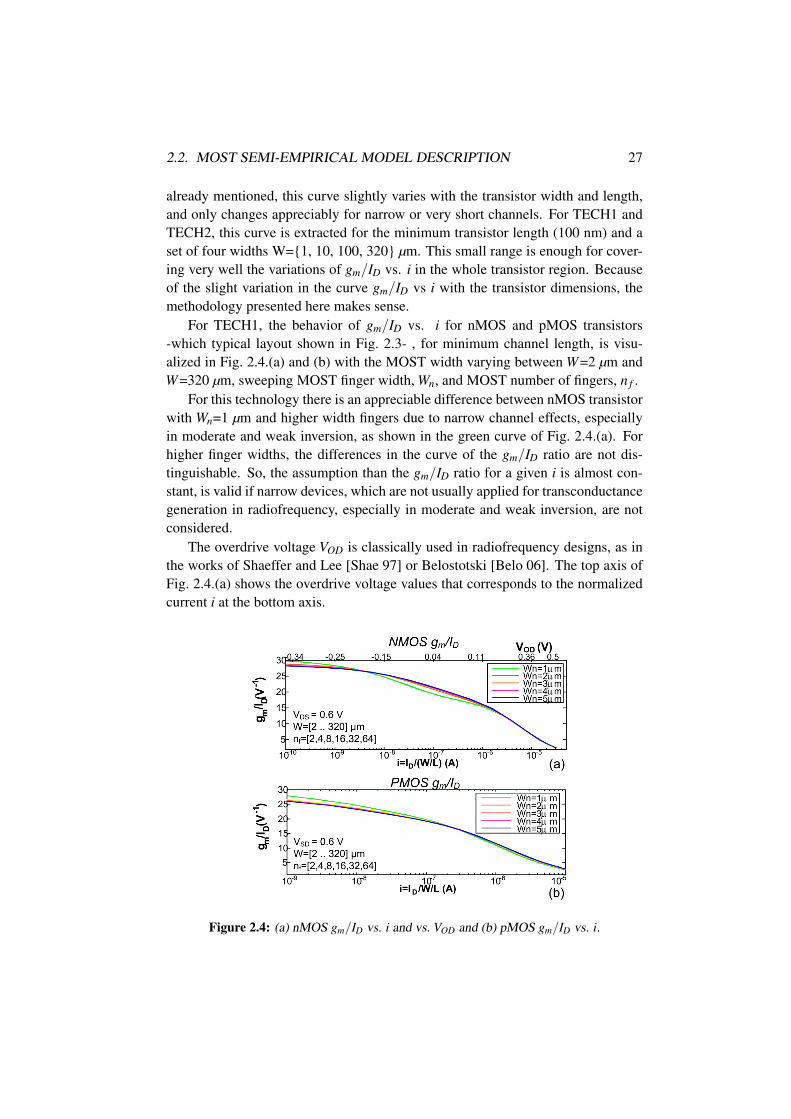
already mentioned, this curve slightly varies with the transistor width and length,
and only changes appreciably for narrow or very short channels. For TECH1 and
TECH2, this curve is extracted for the minimum transistor length (100 nm) and a
set of four widths W={1, 10, 100, 320} μm. This small range is enough for cover-
ing very well the variations of gm/ID vs. i in the whole transistor region. Because
of the slight variation in the curve gm/ID vs i with the transistor dimensions, the
methodology presented here makes sense.
For TECH1, the behavior of gm/ID vs. i for nMOS and pMOS transistors
-which typical layout shown in Fig. 2.3- , for minimum channel length, is visu-
alized in Fig. 2.4.(a) and (b) with the MOST width varying between W=2 μm and
W=320 μm, sweeping MOST finger width, Wn, and MOST number of fingers, n f .
For this technology there is an appreciable difference between nMOS transistor
with Wn=1 μm and higher width fingers due to narrow channel effects, especially
in moderate and weak inversion, as shown in the green curve of Fig. 2.4.(a). For
higher finger widths, the differences in the curve of the gm/ID ratio are not dis-
tinguishable. So, the assumption than the gm/ID ratio for a given i is almost con-
stant, is valid if narrow devices, which are not usually applied for transconductance
generation in radiofrequency, especially in moderate and weak inversion, are not
considered.
The overdrive voltage VOD is classically used in radiofrequency designs, as in
the works of Shaeffer and Lee [Shae 97] or Belostotski [Belo 06]. The top axis of
Fig. 2.4.(a) shows the overdrive voltage values that corresponds to the normalized
current i at the bottom axis.
Figure 2.4: (a) nMOS gm/ID vs. i and vs. VOD and (b) pMOS gm/ID vs. i.

28 CHAPTER 2. MODELING OF NANOMETER RF CMOS PROCESSES
• gm/ID with drain-voltage and technology variations
Lets see now the gm/ID ratio spread variations with the VDS voltage, which are
presented in Fig. 2.5 for VDS={0.3, 0.6, 0.9, 1.2} V, n f ={1, 4, 16, 64} and Wn={2,
3, 4, 5} μm. It is noticeable a deviation when VDS=0.3 V, but it is not so large
to be considered. Previous results show that gm/ID versus VDS variations do not
modify considerably the gm/ID curve, and hence the circuit characteristic in which
this transistor is embedded.
Lets see now the gm/ID variations with technology parameters. Considering
typical, fast and slow corners of the technology TECH1 in Fig. 2.6, we observe a
very slight variation in the gm/ID ratio. This reinforces the idea of utilizing it as
the basis of the methodology we will describe later on.
Figure 2.5: gm/ID versus i for four VDS voltages.
Figure 2.6: nMOS gm/ID corners (typical, fast and slow) versus i.

2.2. MOST SEMI-EMPIRICAL MODEL DESCRIPTION 29
• fT versus gm/ID
The transition frequency definition is
fT =gm
2π(Cgs +Cgd +Cgb)(2.19)
where Cgs, Cgd and Cgb are the gate-source, gate-drain and gate-bulk capacitances
of the MOST. As gm and capacitances can be expressed versus gm/ID, fT is a
function of gm/ID, as it is appreciated for nMOS and pMOS transistors in Fig. 2.7.2
These curves give us an idea of the frequency limits of nMOS and pMOS transistors
of TECH1 using minimun channel length for different inversion regions.
These figures show that for an nMOS transistor biased in SI, fT can surpass one
hundred gigahertz and pMOST reaches fifty gigahertz. In deep WI those frequen-
cies drop down to levels below the gigahertz. For the nMOS transistor of Table 2.1
and considering again the very restrictive quasi-static limit for the working fre-
quency f0 of one tenth of fT , for a gm/ID around 4 V−1, f0 can be up to the tens of
gigahertz, whereas with a gm/ID around 25 V−1 f0 falls below the gigahertz. This
simple check lets the designer to know the limitations of the technology in terms
2The plots comparing the gm/ID and fT as functions of i is presented in Appendix 2.A, Fig. 2.38.
Figure 2.7: (a) nMOS and (b) pMOS fT versus gm/ID.

30 CHAPTER 2. MODELING OF NANOMETER RF CMOS PROCESSES
of frequency in each level of inversion. 3
2.2.2 Output conductance gds and gds/ID ratio
Another fundamental small-signal parameter required in our methodology to de-
scribe the MOST behavior is the output conductance gds. It dramatically increases
in nanometer transistors with respect to micrometer ones due to the shortening of
the channel length, as it is, in a first approximation, inversely proportional to the
transistor length L [Tsiv 00]. This effect should be considered because it could
strongly influence certain RF blocks. For example, in an LC tank-VCO the con-
ductance gds affects the value of the final MOS transconductance chosen, and hence
the bias current and the phase noise; in an LNA a high gds value reduces the maxi-
mum gain of the circuit.
The gds/ID ratio, similar to the gm/ID ratio, is applied here [Jesp 10]. Figure 2.8
shows the behavior of gds/ID versus gm/ID4. The gds/ID range is very small, mov-
ing from 0 to 2 V−1, and no appreciable change in gds/ID is seen when Wn is higher
than 1 μm.
The gds/ID ratio decreases when moving towards strong inversion, which hap-
pens because gds/ID ∼= 1/VA, where VA is the Early voltage in first-order chan-
nel length modulation formula, and as Tsividis stands, in Sections 6.2 and 8.2 of
[Tsiv 00] VAW < VAS with VAW and VAS the Early voltage for weak and strong inver-
sion regions, respectively.
Figure 2.8: nMOS gds/ID versus gm/ID.
3A brief comment concerning the election of the unitary transistor width Wn is that, as expected,
it is recommendable to use transistors with high Wn (and so, less n f ) in moderate and weak inversion,
to reduce the parasitic capacitances. At the limit, for transistors with Wn=1 μm the fT substantially
drops in moderate inversion regions.4The behavior of the gds/ID ratio versus i is presented in Fig. 2.39.

2.2. MOST SEMI-EMPIRICAL MODEL DESCRIPTION 31
• gds/ID with drain voltage and technology variations
Contrary to what happens with the gm/ID ratio, the gds/ID ratio appreciably
changes with the drain-source voltage VDS, which is expected due to the direct
relation of gds with the drain voltage. In Fig. 2.9, the gds/ID ratio is plotted ver-
sus gm/ID, for four drain voltages, where the variation is clearly appreciable. A
decreasing tendency of the gds/ID curve is observed when drain voltage increases.
In weak and strong inversion regions gds/ID changes around 0.7 V−1 and 0.4 V−1,
respectively.
The corners variations of the gds/ID parameter are presented in Fig. 2.10. In or-
der to provide a typical example, only the corners obtained with VDS=0.3 V are plot-
ted. The high spread of gds/ID between typical and fast and slow corners reaches
0.5 V−1.
The gds MOS parameter has a considerable spread with variations in the drain
voltage and in the technology characteristics. These facts make us expect some
differences between computational data and simulations if the correct drain voltage
is not chosen; and between computational data and measurements if the process
moves from typical corner.
Figure 2.9: gds/ID versus gm/ID for four drain voltages.
Figure 2.10: nMOS gds/ID corners versus gm/ID, for VDS=0.6 V.

32 CHAPTER 2. MODELING OF NANOMETER RF CMOS PROCESSES
2.2.3 MOST extrinsic and intrinsic capacitancesWorking in radiofrequency compulsory requires the inclusion of transistor capac-
itances in the MOST modeling, which are grouped in intrinsic and extrinsic ones.
They influence not only on the fT computation but also on the input and output
impedances of the MOS, the MOST gain and noise, among other characteristics.
In this thesis, the extrinsic capacitances are modeled with the known expres-
sions of [Tsiv 00] (Section 8.4, pages 405-410):
1. the extrinsic gate-source (and gate-drain) capacitances Cgse=Cgde=WC′′o , with
C′′o the capacitance per unit width that includes the fringe, the overlap and the
top gate contributions.
2. the extrinsic gate-bulk capacitance Cgbe = 2LC′′ob, where C
′′ob is the capaci-
tance per unit length.
3. the junction substrate-source and substrate-drain capacitances Cbse = Cbde =AS(D)C
′js( jd) + lS(D)C
′′js f ( jd f ) + WC
′′jsc( jdc), with AS(D) and C
′js( jd) are the
source (drain) area and the capacitance per unit area, lS(D) and C′′js f ( jd f ) are
the source (drain) outer sidewall length and the capacitance per unit length
and W and C′′jsc( jdc) are the source (drain) inner sidewall length the capaci-
tance per unit length.
The parameters of the extrinsic capacitances are taken from the technology files
and from layout considerations.
Respect to the intrinsic capacitances, the study is a bit more complex. Consid-
ering again that the working frequencies are below one tenth of fT , it is enough
to consider the following intrinsic capacitances: Cgs, Cgd , Cgb, Cbs and Cbd , dis-
regarding the other four capacitances and transcapacitances as well as non-qua-
sistatic effects. These capacitances change with the inversion level, as Tsividis
states ([Tsiv 00], page 405); and obviously they change with the transistor size. In
this work the intrinsic capacitances are considered to be proportional to the gate
area (WL). This can be done because these capacitances are proportional to the
oxide capacitance Cox which is itself proportional to WL, as Tsividis presents in
[Tsiv 00], Section 8.3, page 391. Considering this basic idea, in the LUTs of the
MOST there are the normalized capacitances C′i j versus the gm/ID.
In Fig. 2.11 it is shown the behavior of the normalized capacitances C′gs, C
′gd ,
C′gb, C
′bs and C
′bd versus gm/ID for VDS=0.6 V and a wide set of MOST widths. Their
maximum absolute spread are: (1) the C′gs variation is around 1 mF/m2; (2) the C
′gd
spread is around 0.4 mF/m2; (3) the C′gb error it is less than 0.02 mF/m2, being
the highest perturbation in the MI-WI zone, as the inset of Fig. 2.11.(c) stands; (4)
the C′bs variation is 0.02 mF/m2 and (5) the C
′bd error is lower than 0.002 mF/m2.

2.2. MOST SEMI-EMPIRICAL MODEL DESCRIPTION 33
Figure 2.11: Intrinsic capacitances: (a) C′gs, (b) C
′gd , (c) C
′gb, (d) C
′bs and (e) C
′bd versus
gm/ID. The inset of (c) shows that the highest perturbation of the C′gb is in MI-WI zone.
Only for C′gs the error is appreciable in weak inversion, where C
′gs rounds 4 mF/m2
and the relative error is around 20%. Despite this error in this region, in the first ap-
proach, the normalized capacitance LUTs only consider the variations with gm/ID.
Taking into account this basic idea, in the LUTs of the MOST there are the
normalized capacitances C′i j=Ci j/(WL) versus gm/ID.
Considering drain-source voltage variations, Fig. 2.12 shows that the spread is
very similar that when the width is swept. To study the corners, we extract the C′gs
of a MOST with W=8 μm and VDS=0.6 V; which expected slight spread is shown

34 CHAPTER 2. MODELING OF NANOMETER RF CMOS PROCESSES
in Fig. 2.13. In all cases, the tolerances are acceptable for this methodology. Af-
terwards, normalized capacitances are used to estimate the capacitances of other
transistors in the considered width range, only multiplying by the respective WL.
With the observed results, a rough capacitance modeling can be obtained by ex-
tracting the capacitances of a MOST sized with a middle-range width and biased
with a midst-range VDS.
Figure 2.12: C′gs versus gm/ID for four VDS.
Figure 2.13: C′gs corners versus gm/ID

2.2. MOST SEMI-EMPIRICAL MODEL DESCRIPTION 35
2.2.4 Noise in MOS transistors
This section presents the MOS transistor noise sources used throughout this work to
deduce the equations that describe the noise characteristics of the radio-frequency
blocks. These sources are fundamentally the drain-noise current (consisting of the
white noise and the flicker noise) and the induced gate noise, presented in Tsividis
([Tsiv 00] Section 8.5); and more recently, for RF models, by Shi et al. [Shi 09].
The scheme of these noise currents referred at the output drain of the MOS as i2o( f ),as well as its principal contributors are shown in Fig. 2.14.
The output current power spectral density zone is sketched in Fig. 2.14, in
which three regions are recognized: the flicker noise zone, the white noise zone
and the induced-gate noise zone. The white noise is due to random fluctuations of
the charge in the channel, the flicker noise is the result of trapping and detrapping
of the channel carriers in the gate oxide. The frequency of the asymptotic limit
between these two zones fc, is called the corner frequency.
The white noise power spectral density (psd) i2w,d , for all inversion regions, is
expressed as [Galu 99]
i2w,d = 4kBT γgd0 = 4kBTγα
gm (2.20)
where kB is the Boltzmann constant, T is the absolute temperature, γ is the excess
noise factor, α is equal to α = gm/gd0, with gd0 the output conductance gds at
VDS = 0. gd0 is considered because at zero VDS the white noise is maximum for
all-inversion regions [Tsiv 00].
Figure 2.14: Sketch of the MOST power-spectral density versus frequency; with the gate
noise psd and drain noise psd order of magnitudes at f0 and |Γ( f )|2 the transfer funcion of
the induced gate noise to the MOST i2o.

36 CHAPTER 2. MODELING OF NANOMETER RF CMOS PROCESSES
The flicker noise psd i21/ f ,d is written as
i21/ f ,d =
KFg2m
C′oxWL
1
f(2.21)
with KF the flicker noise constant, C′ox the normalized MOST thin oxide capaci-
tance and f is the frequency of study.
The psd of the drain-noise current is i2d = i2w,d + i21/ f ,d as no correlation is sup-
posed to exist between the white noise and the flicker noise sources.
For high frequency operation, the induced gate noise should be considered, as
it is pointed out in Fig. 2.14. This noise appears because random fluctuations of
the carriers (generated by the white noise) cause a gate current to flow through the
gate, even if no signal current exists. Its psd, i2g, is expressed as
i2g = 4kBT δC2
gs
5gd0
4π2 f 2 =16
5π2kBT αδ
C2gs
gmf 2 (2.22)
where δ is the gate noise coefficient.
The gate noise is partially correlated with the drain noise due to the white noise,
with a correlation coefficient c given by Van der Ziel [Ziel 86] and Lee [Lee 04]
c =igi∗w,d√i2gi2w,d
(2.23)
with |c| approximately equal to 0.4.
• Noise constants versus gm/ID
The generally used values of γ, δ and α are γ = 2/3, δ is two times γ and α ∼=0.6. But when working with short channel devices and in moderate and weak
inversion, these parameters would take different values. These parameters depend,
as happens with other transistor characteristics, on gm/ID. So, in order to improve
the methodology results, we express these constants in terms of gm/ID to include
them in the design methodology.
When a fluctuation of these parameters does not modify considerably the noise
characteristics of a circuit, it is acceptable to consider them as constants. In Chap-
ter 3 it is provided a set of VCO designs in the mentioned situation. However,
when a small change in them modifies the circuit noise characteristics, a deeper
study must be done as it happens with the LNAs of Chapter 4.
To show graphically the effects of the inversion region in the noise parameters
α and γ, they have been extracted from simulations using a 48 μm×100 nm MOS
transistor (with Wf =3 μm and n f =16) and plotted in Fig. 2.15, for four VDS voltages.

2.2. MOST SEMI-EMPIRICAL MODEL DESCRIPTION 37
Figure 2.15: nMOS transistor noise parameters: γ, α and γ/α.
As the relation γ/α also appears in the noise equations of this dissertation, it is also
represented there. For strong inversion, γ and α are low, but not always near the
generally used values. However, when moving to weak inversion, both variables
suffer a dramatical raise. This increment generates circuit noise computation errors
if the MOS transistor is in MI and WI and the proper parameter values are not
considered. Nonetheless, when considering the γ/α ratio, it is maintained relatively
constant.
Extending this study to the process variations, Fig. 2.16 depicts the simulated
α versus gm/ID considering the four corners, for a set of VDS voltages; as happens
with other MOST characteristics, the slight spread observed might not be included
in the MOST LUTs.
Figure 2.16: α corners versus gm/ID for four VDS.

38 CHAPTER 2. MODELING OF NANOMETER RF CMOS PROCESSES
Figure 2.17: KF versus gm/ID for three frequencies and four VDS.
Lets now consider the KF parameter. KF is solved extracting by simulation the
flicker current density and the transconductance while sweeping gm/ID. The study
is done with a 48μm/100nm MOST, for three frequencies f0={2.4 GHz, 100 kHz
and 10kHz} and four VDS, as it is presented in Fig. 2.17. No appreciable differences
are visualized when varying the drain voltage. However, there is a clear variation
of KF when the working frequency is considered. Table 2.2 lists a set of values
of KF in weak, moderate and strong inversion, for the three frequencies simulated.
Two observations arise from observing the presented data: (1) KF decreases when
Table 2.2: Comparison of KF values for SI, MI and WI.
f0 (Hz) gm/ID (V−1) KF (×10−24) at VDS=0.6 V
2.4 G 5 48
100 k 5 11
10 k 5 8.1
2.4 G 14 22
100 k 14 4.8
10 k 14 3.0
2.4 G 21 12
100 k 21 2.7
10 k 21 1.7

2.2. MOST SEMI-EMPIRICAL MODEL DESCRIPTION 39
moving to weak inversion for all the frequencies considered, and (2) the estimation
of KF increases for high frequencies.
Concerning the variation with the inversion region, two approaches could be
taken. A simple approach is to consider the mean value of KF through the range of
gm/ID and an advanced approach is to use look-up tables. Depending on the circuit,
the level of accuracy needed in the estimation of the flicker noise and the ratio
between i2d,1/ f and i2d,w is the approach that should be considered. For example, in
the LNA design methodology of Chapter 4 it is used the simple approach.
Noise parameters vary very slightly with the transistor width (with a relative
error of less than a 5% for γ/α and KF ), so this variation is not considered here.
Further reading on these topics can be found in the studies presented by Man-
ghisoni et al. [Mang 06], Scholten et al. [Scho 04] or Chan et al. [Chan 06]. These
works quantify the constants of the power spectral densities of MOS transistor
noise sources particularly for nanometer technologies.
2.2.5 Overdrive voltage versus gm/ID
As it is expressed in (2.5), the overdrive voltage is function of the normalized cur-
rent, and hence of the gm/ID ratio. It means that the designer has a way of directly
estimate the value of VGS when the gm/ID ratio is fixed. As happens with other
MOS transistor characteristics, it varies slightly with the MOST width, as it is
shown in Fig. 2.18.
It has been studied the variation of the overdrive voltage with the drain-source
voltage, presented in Fig. 2.19 and its spread with the corners (typical, fast and
slow), for a fixed drain-source voltage, plotted in Fig. 2.20. As well as happens with
the MOST width variations, the maximum spread considering the VDS variations is
around 0.03 V, then it is not needed to include these variations in the LUTs. The
variations with the corners are around the same value.
Figure 2.18: Overdrive voltage versus gm/ID varying the transistor width, for VT =0.41 V

40 CHAPTER 2. MODELING OF NANOMETER RF CMOS PROCESSES
Figure 2.19: Variations with the VDS of the overdrive voltage versus gm/ID .
Figure 2.20: Corners of the overdrive voltage versus gm/ID varying the transistor width.
2.2.6 Bulk substrate effectThis is considered a second order effect because gmb is much smaller than gm, as
it is shown in Fig. 2.21. However it should be included in the LUT, especially if
this effect is important in the circuit behavior. For other circuits, where the bulk is
short-circuited with the source terminal, it is discarded.
Figure 2.21: gm/gmb ratio as function of gm/ID.

2.2. MOST SEMI-EMPIRICAL MODEL DESCRIPTION 41
For the common-source LNA of Chapter 4, the bulk effect present in the cas-
code MOST is neglected because this transistor affects in a much less extend the
LNA behavior respect to the MOST amplifier. For the VCO, only the pMOS tran-
sistors have the bulk effect, but in the first approach is has been discarded to sim-
plify the set of equations presented.
2.2.7 MOS transistor data acquisition schemeTo conclude, for the proposed methodology five MOS transistor basic characteris-
tics must be considered, for a fixed VDS:
1. the transconductance to current ratio gm/ID,
2. the output conductance to current ratio gds/ID,
3. the normalized MOS capacitances C′i j=Ci j/(WL),
4. the noise constants
5. the overdrive voltage
To acquire these LUTs, the simple scheme of Fig. 2.22 is utilized. In it, MOS
transistor gate, drain and source nodes are connected to a DC voltage source, while
source and bulk nodes are connected either to ground (nMOS transistor) or to the
supply voltage (pMOS transistor). VG is swept extracting ID, gm, gds and C′i j. VD
and VS are set around their expected DC value. The same simulation must be run
for a set of widths -for example, the mentioned set of {1, 10, 100, 320} μm-,for
a fixed transistor length. If the transistor length also changes, following the same
idea, a small set of lengths (e.g. 100 nm, 1 μm, 10 μm) should be chosen. For the
noise parameter extraction, an AC noise analysis has to be done.
Figure 2.22: Test circuit for acquiring MOST gm/ID, gds/ID and C′i j.

42 CHAPTER 2. MODELING OF NANOMETER RF CMOS PROCESSES
2.3 Passive component semi-empirical modelsIn radiofrequency design, on-chip passive components need to be correctly charac-
terized, since the performance of the circuit strongly depends on them. For exam-
ple, in a VCO design, if the model of the tank inductor considers a parasitic parallel
resistor much lower that the real one, the VCO could even not oscillate. This sec-
tion briefly introduces the models and parameters of the passive components we
will use in the designs of Chapters 3 and 4.
The passive components can be modeled either with analytical models or with
semi-empirical ones. The former are especially useful in multi-frequency systems.
However obtaining simple and accurate formulae for the element and its parasitics
is somewhat difficult. In this thesis we decided to use semi-empirical models ex-
tracted from electrical simulations, the same way we do with the MOS transistor
modeling. Depending on the level of accuracy and the available technological in-
formation, the models can be extracted using the parametrized cells provided by
the foundry libraries or the ones obtained with electromagnetic simulators as ADS
Momentum, ASITIC [Nikn 00] or VPCD of Cadence [VPCD 09]. Two main draw-
backs of electromagnetic simulators exist: 1) the need to have the technological
data provided by the foundry to obtain accurate descriptions, and 2) the high com-
putational time spent to obtain the solutions. In this thesis, in order to speed-up the
design, the former method is utilized; the library cells supplied by the foundry are
simulated using AC analysis at the working frequency obtaining their equivalent
complex impedance.
This thesis uses simple AC passive component models, as an ideal inductor in
series with a parasitic resistor for on-chip inductors. Biunivocal relations between
the model parameters of the component are very useful to generate a simple design
flow, as for example between the inductor inductance and its parasitic serial resis-
tance The extraction of these models depends on the topological location of the
component; for example, if the device has an AC grounded terminal or it is fully
differential. The analysis performed with the electrical simulator has to reflect this
fact.
In the following study, a simple modeling of the inductors, capacitors, varactors
and resistors is presented as well as their principal characteristics and their para-
sitics. Despite the varactors are, in fact, based on active devices, we include their
study in this section. We do this because we characterize the varactor, for each
value of its control voltage, as a capacitor with its equivalent capacitance and its
parasitic resistance.

2.3. PASSIVE COMPONENT SEMI-EMPIRICAL MODELS 43
2.3.1 Inductor modelingIn this thesis we use the inductors cells provided by the foundry. The extracted
inductor model consists on an equivalent ideal inductor with a parasitic resistor for
the working frequency f0. Depending on the use of the inductor in the circuit is
the way it is analyzed, i.e. if it is a differential inductor or an inductor with an AC
grounded port. The scheme of Fig. 2.23 shows the way we perform the study, using
the AC analysis. Considering a single-ended inductor, one of its ports is connected
to the source and the other is grounded. For a differential inductor, its middle port
is AC grounded and the other two are connected to identical sources with a phase
difference of 180◦ in order to consider the differential voltages between these ports.
With the latter analysis, its serial or parallel networks are found.
The inductor has a complex series impedance
Zind = Rs,ind + jXs,ind = Rp,ind// jXp,ind (2.24)
where Rs,ind and Rp,ind are the parasitic series and parallel resistances and Xs,ind and
Xp,ind are the series and parallel reactance, respectively. The reactances, divided by
the angular frequency ω0 = 2π f0, are the equivalent series and parallel inductance
Ls,ind and Lp,ind .
The inductor quality factor is defined as
Qind =Xs,ind
Rs,ind=
Rp,ind
Xp,ind(2.25)
The equivalent inductance of the parallel network is
Lp,ind = Ls,ind(1+1/Q2ind) (2.26)
and the parasitic parallel resistance of the parallel network is
Rp,ind = Rs,ind(1+Q2ind). (2.27)
For real on-chip inductors with Qind ≥ 4, Lp,ind∼= Ls,ind = Lind .
Figure 2.23: (a) Parallel inductor modeling and (b) schematic of AC analysis for single-
ended and differential inductors.

44 CHAPTER 2. MODELING OF NANOMETER RF CMOS PROCESSES
Figure 2.24: Inductor layout and physical characteristics: coil widths, number of turns and
radius.
Figure 2.25: (a) Parallel resistance, (b) series resistance and (c) quality factor versus Lind
for f0=2.4 GHz, for four inductor widths, up to sixteen internal radius (rad) and up to 21
turns (turn). Maximum parallel resistance and minimum series resistance for each feasible
inductance is marked with a black line.

2.3. PASSIVE COMPONENT SEMI-EMPIRICAL MODELS 45
Figure 2.26: Inductors LUTs: maximum parallel parasitic resistance and minimum series
parasitic resistance for each feasible inductance in the reference technology.
In these conditions the semi-empirical model of inductors contains Rmins,ind and
Rmaxp,ind versus Lind for a certain working frequency f0, where Rmin
s,ind and Rmaxp,ind are
the minimum Rs,ind and maximum Rp,ind for all the possible inductors of the tech-
nology. Considering these relations, the first step in the characterization of a set of
technology inductors is to run the AC analysis for a large set of inductors, varying
the inductor turns (turn), coil widths (w) and internal radius (rad) (which are shown
in the layout of Fig. 2.24, in order to obtain a complete collection of modeled de-
vices characteristics, i.e. Rs,ind , Rp,ind , Qind for Lind .
For TECHNO1, the LUTs include the scatter plots of Fig. 2.25, when both
coil inductor width, internal radius and number of turns are swept. The minimum
quality factor Qind of the selected inductors is 5, to be far from the self resonance
frequency of the device. The second step is to collect two inductor LUTs, Λ(s)L and
Λ(p)L , where for each inductance value, we get the lowest series and the highest par-
allel resistance, respectively, and the geometric aspect of its implementation. The
results are displayed in the black lines of Fig. 2.25.(a) and (b), for Rp,ind and Rs,ind ,
versus Lind , and replotted separately in Fig. 2.26. The characterization has been
made dense enough to cover the whole range of inductances with a logarithmic
grid of 20 points per decade. This fact will be justified at the end of Section 4.1.3.
The data in these plots show that for this technology the highest parallel resistances
come with the largest inductor values whereas lowest serial resistance values cor-
respond with low inductor values.

46 CHAPTER 2. MODELING OF NANOMETER RF CMOS PROCESSES
Figure 2.27: Rmins,ind and Rmax
p,ind corners versus Lind for f0=2.4 GHz.
Serial and parallel resistances as well as the inductances will change with tech-
nology variations. Here it is presented the process corners variations of the serial
and parallel resistances versus Lind in Fig. 2.27. Due to the slight change with the
corners, it can be concluded that in a first approximation the corners cannot be
taken into account in the variations of the designs characteristics.

2.3. PASSIVE COMPONENT SEMI-EMPIRICAL MODELS 47
2.3.2 Capacitor and varactor modeling
As well as inductors, we model the capacitors and varactors as AC serial or parallel
networks, depending on their use in the circuit. Figure 2.28.(a) sketch the parallel
network that model these devices. This network consists of a reactance in parallel
with the parasitic resistance. It can be transformed into an AC serial network as
Zcap = Rp,cap//− jXp,cap = Rs,cap − jXs,cap (2.28)
where Rs,cap and Rp,cap are the serial and parallel parasitic resistances and -Xs,capand -Xp,cap its series and parallel reactances. Then, the equivalent parallel capaci-
tance Cp,cap is
Cp,cap = 1/(2π f0Xp,cap). (2.29)
where f0 is the working frequency. The quality factor, Qcap is
Qcap = Rp,cap/Xp,cap = Xs,cap/Rs,cap, (2.30)
thus, the relations between the series and the parallel resistances and capacitances
are
Rs,cap =Rp,cap
Q2cap +1
, (2.31)
and
Cs,cap = Cp,cap
(1+
1
Q2cap
). (2.32)
When Qcap ≥ 4 parallel and serial capacitances could be considered equal, i.e.
Cp,cap = Cs,cap = Ccap.
Figure 2.28: (a) Parallel capacitor/varactor modeling. (b) Single-ended and (c) differential
scheme of the varactor parameter extraction.

48 CHAPTER 2. MODELING OF NANOMETER RF CMOS PROCESSES
The semi-empirical model includes in the LUTs Ccap, Rmins,cap and Rmax
p,cap, where
Rmins,cap and Rmax
p,cap are the minimum serial and maximum parallel resistances of the
feasible technology capacitors. The same is applied for the varactors. As well as
for the inductors, AC analysis is again utilized to characterize these components
and generate the correspondent LUT, for capacitors with Qcap ≥ 5 to be far from
the self resonance frequency of the device. The LUT collects Rp,cap, Rs,cap, Qcapand Ccap as well as the capacitor dimensions for each capacitor sizing.
• Capacitors
This section briefly presents the features of the capacitors used in this thesis, the
Metal-Insulator-Metal (MIM) capacitors, which layout is shown in Fig. 2.29. As
well as the inductors, the first step in the characterization is to run an AC analysis
for a considerable number of devices to collect their characteristics. Varying their
width w and length l, we collect the data shown in Fig. 2.30, where the scattering
plots cover w and l between 4 μm and 30 μm.
The second step is to collect two capacitor LUTs, Λ(s)C and Λ(p)
C , where for
each capacitance value we extract the lowest series and highest parallel resistance,
respectively. This step is graphically represented in the black lines of Rs,cap and
Rp,cap versus Ccap of Fig. 2.30.(a) and (b).
These data show the very high quality factors of the MiM capacitors, above 50
for Ccap below 2 pF, and that the parallel/serial resistances are sufficiently high/slow
in all cases. This leads us to make a simplification in the capacitor design used in
this work, imposing a physical constraint over the capacitor sizing: w and l are
equally set. We gain in design simplicity without loosing design quality. In Ap-
pendix 2.B the curves of Rs,cap, Rp,cap and Qcap versus Ccap for w = l are presented.
From the corresponding plots some conclusions arise. Considering the serial
parasitic resistance, it increases up to 6 Ω for very small capacitances and decreases
to less than 1 Ω for capacitors higher than 1 pF, so if serial resistance is a strong
Figure 2.29: Layout of the MiM capacitors, showing their width (w) and length (l) param-
eters.

2.3. PASSIVE COMPONENT SEMI-EMPIRICAL MODELS 49
Figure 2.30: MiM capacitors (a) serial and (b) parallel parasitic resistances and (c) quality
factor versus Ccap, varying w and l.
constraint in the design, very low capacitances could not be used. Next, when
parallel parasitic resistance is studied, it is observed that small capacitors have
very high resistances (higher than 300 kΩ), whereas for high capacitances those
values fall down to 2 kΩ. Then, for designs where high parallel resistance values
are compulsory, there are maximum values of w and l above which the capacitors
cannot be used. The capacitance quality factor Qcap have values over the hundred
for Ccap below 1 pF and over fifty for Ccap between 1 pF and 2 pF.
To complete this study we present the simulations for typical, slow and fast
corners for Rmins,cap and Rmax
p,cap. The results are resumed in Fig. 2.31. For low values
of Ccap (below 200 fF) the spread of Rmaxp,cap and Rmin
s,cap is noticeable. However,
this variation does not reduce enough the parallel resistance (or dows not increase
the serial resistance) to make them have a very low quality factor; meaning that
the spread due to the corners for low capacitor values is not important. For high
capacitor values, the spread is mainly in the resulting capacitance - as shown with
the bubble of Fig. 2.31.(c)-, and would modify the design results.

50 CHAPTER 2. MODELING OF NANOMETER RF CMOS PROCESSES
Figure 2.31: Corner simulations results for: (a) Rmins,cap, (b) Rmax
p,cap and (c) Qcap vs Ccap for
f0=2.4 GHz.
The low serial and high parallel resistances, as well as the high quality factors of
these capacitors permit considering the MIM capacitors as almost-ideal devices, in
comparison with inductors or transistors. It appreciably simplifies the circuit design
and the creation of design methodologies, as we will see later on. Therefore, for
very high-Q values (above 50), the capacitors are considered as ideal in this thesis.

2.3. PASSIVE COMPONENT SEMI-EMPIRICAL MODELS 51
• Varactors
Varactors are generally based on semiconductor devices and have much lower qual-
ity factor than MiM capacitors. In this work, both TECH1 and TECH2 provide
MOS accumulation varactors. Their quality factors could be comparable with the
ones of high-Q on-chip inductors. Also their parasitic resistances suffer from vari-
ations when the tuning voltage Vtune (at the drain-source terminal), the DC voltage
V DCG and the amplitude voltage V RF
G at the gate, changing the effective capacitance
[Hega 03]. As a result, a study should be done for different design conditions. As
varactors are very dependent on the signal amplitudes, it is not always possible to
use a AC analysis as it is a small-signal analysis. For these devices, we need a
large-signal analysis, and in this case we utilize the PSS analysis of the SpectreRF
simulator of CADENCE. It enables us to calculate the impedance Zvar seen be-
tween the terminals G-D/S at the working frequency f0, i.e. Zvar = V ( f0)/I( f0),where V and I are the phasors in f0 of vvar and ivar of Fig. 2.28.(b). This way we
obtain the effective serial resistance Rs,var, the effective parallel resistance Rp,varand capacitance Cvar at the working frequency. As in this dissertation we only use
the varactors in the VCO design (Chapter 3), this study is only focused on this par-
ticular application; Vtune is fixed to 0.5 V (in the middle of its range), V RFG is set to
400 mV and V DCG is fixed to 500 mV, which are representative voltages in the VCO
implementation.
As well as the inductor or capacitor previous approaches, the serial network
is initially used to characterize a varactor. Their serial resistance and equivalent
capacitance are, respectively, Rs,var and Cvar. Again, it is possible to transform
this network into a parallel one, utilizing the expressions (2.31) and (2.32). Fig-
ure 2.28.(b) and (c) show the employed data extraction scheme for varactors.
In this thesis, single-ended varactors are not used stand-alone; instead, only var-
actors in the differential configuration are implemented, as shown in Fig. 2.28(c).
As the differential architecture is formed by two single-ended varactors and, as their
drain voltage is ideally fixed to a Vtune value, this study of single-ended varactors
is still valid here.
The first step is to collect the features of a considerable amount of devices. The
varactors of TECH1 have a fixed finger of W/L=1.6 μm/400 nm, and the designer
can sweep both the number of fingers f ng and the number of rows of these fingers
grp (as shown in Fig. 2.32). In this study f ng={1,4,8,16,32} and grp is swept from
1 to 16. The results of Rs,var, Rp,var and Qvar versus Cvar are presented in Fig. 2.33.
The second step is to collect two varactors LUTs, Λ(s)V and Λ(p)
V for the lowest
series and largest parallel resistance for each feasible effective capacitance. The
corresponding results are shown in Fig. 2.33.(a) and Fig. 2.33.(b) with square sym-
bols.
Figure 2.34 shows the variation in the LUT varactor characteristics (Λ(s)V and

52 CHAPTER 2. MODELING OF NANOMETER RF CMOS PROCESSES
Figure 2.32: Layout of the varactors of TECH1, showing the involved parameters f ng and
grp.
Figure 2.33: (a) Rs,var, (b) Rp,var, (c) Qvar versus Cvar. The squared markers shows (a) the
minimum series and (b) maximum parallel parasitic resistances.

2.3. PASSIVE COMPONENT SEMI-EMPIRICAL MODELS 53
Figure 2.34: (a) Rmins,var and (b) Rmax
p,var versus Cvar for f0=2.4 GHz.
Λ(p)V ) for typical, fast and slow corners. The maximum spread is 17 Ω for the Rmin
s,varand 15 kΩ for the Rmax
p,var for low capacitance values, which is acceptable for the
absolute parasitic values of the varactors.

54 CHAPTER 2. MODELING OF NANOMETER RF CMOS PROCESSES
2.3.3 Resistor modelingIn this section there are only studied resistors with low resistances values. The
reason is that they would be used to adjust the input or output impedances of RF
circuits, as LNAs. Applications that include high resistances are not considered
in this thesis, so modeling these elements are out of the scope of this study. The
technologies used have several types of integrated resistors but we only discuss here
the characteristics of the RF characterized P+ Poly resistors with silicide, which are
appropriate when low resistance values are needed in RF. The model presented here
is used only when the resistor is in an RF path.
As well as inductors and capacitors, integrated resistors have associated para-
sitics, and therefore, we could model it accordingly with an AC analysis. Depend-
ing on the resistor type and size, its equivalent parasitic in AC could be capacitive
or inductive. As the monolithic resistors studied have low resistance values, it is
more convenient to model them as a resistor Rres in series with a series reactance
Xs,res, as shown in Fig. 2.35 with its correspondent quality factor Qres, defined as
Qres =Rres
|Xs,res| . (2.33)
The semi-empirical model of the resistor includes Xmins,res, which is the minimum
Xs,res for each feasible resistor value of the technology and the correspondent Rres.
The resistance of the P+ Poly resistors with silicide is set fixing their width
w and length l. In this work the width is swept from 2 μm to 10 μm despite it
can be further reduced to less than 0.5 μm. Is is done in order to position at least
6 contacts in each resistor’s terminal to reduce the equivalent contact resistance.
Then, the study is done performing an AC analysis for l ∈ [2×w,150 μm] and
w = 2,3,5,8,10 μm. This first step in the characterization is to collect the device
characteristics Rres, Xs,res and Qres, as it is shown in the scattered plots of Fig. 2.36.
The second step is to collect the resistor LUT Λ(s)R , where for each resistance
value it is found the lowest |Xs,res|, and the geometric sizing of each implementa-
tion. These values are highlighted in Fig. 2.36.(a) with the square symbols.
Figure 2.35: (a) Series resistor model, where the reactance can be capacitive or inductive,
and (b) AC simulation scheme.

2.3. PASSIVE COMPONENT SEMI-EMPIRICAL MODELS 55
Figure 2.36: P+ Poly resistor characteristics:(a) Xs,res vs Rres, (b) Qres vs Rres, for
f0=2.4 GHz.

56 CHAPTER 2. MODELING OF NANOMETER RF CMOS PROCESSES
Figure 2.37: Xmins,res corners versus Rres.
Finally, to study the variations in the resistor characteristics we present the re-
sults of the typical, fast and slow corners for the optimum resistances ( represented
by square symbols of Fig. 2.36.(a)) in Fig. 2.37. In the plot it is highlighted the
spread of the reactance and quality factor values when the corner changes for two
cases, low and high resistances. |Xs,res| are always below 1 Ω and Qres always
above 100, so these variations will not be appreciable in the circuit behavior.

2.4. CONCLUSIONS 57
2.4 ConclusionsIn this chapter we presented the implementation of the first two steps of the de-
sign methodology of Chapter 1, including the semi-empirical models adopted for
all the devices used in the design methodology. We review the MOS transistor
model for all-inversion regions, studying the curve gm/ID versus i and the behavior
of fT when the bias point moves from weak inversion to strong inversion region.
We show the importance, already highlighted by other works, of working with a
MOS transistor model that covers all-inversion regions of operation and therefore
exploiting to its maximum the MOS transistor potential and the performance trade-
offs. We show that for RF circuits integrated in nanometer technologies, the best
trade-off occurs in many cases in the moderate region.
We study the behavior of the transistor characteristics gm/ID ratio, gds/ID ratio,
gds, C′i j, VOD and noise parameters for changes in the size,the drain voltage or the
technology characteristics in order to know the limitations of the last two steps of
the general design methodology.
Finally, an analysis of the main passive components of an RF design as induc-
tors, capacitors and resistors is also developed, evaluating for a typical nanometer
RF CMOS technology its modeling, its parasitics and quality factors, and the vari-
ations with corners.
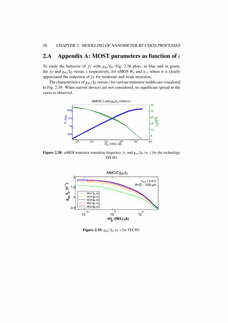
58 CHAPTER 2. MODELING OF NANOMETER RF CMOS PROCESSES
2.A Appendix A: MOST parameters as function of i
To study the behavior of fT with gm/ID, Fig. 2.38 plots, in blue and in green,
the fT and gm/ID versus i, respectively, for nMOS Wn and n f , where it is clearly
appreciated the reduction of fT for moderate and weak inversion.
The characteristics of gds/ID versus i for various transistor widths are visualized
in Fig. 2.39. When narrow devices are not considered, no significant spread in the
curve is observed.
Figure 2.38: nMOS transistor transition frequency fT and gm/ID vs. i for the technology
TECH1.
Figure 2.39: gds/ID vs. i for TECH1.

2.B. APPENDIX B: CAPACITORS MAPS WITH W = L 59
2.B Appendix B: Maps of capacitors obtained withw = l
As discussed in this chapter the physical constraint for MiMs of w = l is considered
in the rest of the work. Therefore, sweeping w=l and applying the electrical AC
analysis, the data of serial, and parallel resistances and capacitances are collected.
Then, fixing this constraint, a look-up table is obtained, in which for each w, and
therefore each Ccap, exists a one-to-one relation with a Rs,cap, Rs,cap and Ccap.
These relations are shown in Fig. 2.40.(a), (b) and (c), where the serial resistance
Rs,cap, parallel resistance Rp,cap and quality factor Qcap versus Ccap are visualized.
Finally, for w = l, the corners for Rs,cap, Rp,cap and Qcap are visualized in
Fig. 2.41. The spread in the parasitic resistances and the quality factor is not sub-
stantial as the serial/parallel parasitic resistance are maintained low/high.
Figure 2.40: (a) Serial resistance, (b) parallel resistance and (c) quality factor versus serial
capacitance for MIM capacitors with equal width and length, for f0=2.4 GHz.

60 CHAPTER 2. MODELING OF NANOMETER RF CMOS PROCESSES
Figure 2.41: Corner simulations for: (a) Ccap versus w; (b) Rs,par, (c) Rp,cap and (d) Qcap
versus Ccap, for f0=2.4 GHz.

2.C. APPENDIX C: TECH2 TECHNOLOGY CHARACTERISTICS 61
2.C Appendix C: TECH2 technology characteristics
Figure 2.42: (a) gm/ID and (b) gds/ID vs. i = ID/(W/L) for four nMOS transistors and
a VDS = 600 mV . Typical limits of strong (SI), moderate (MI) and weak (WI) inversion
regions are shown.
Figure 2.43: gm/ID and fT versus ID of a pMOS transistor with an aspect ratio of
360 μm/100 nm.

62 CHAPTER 2. MODELING OF NANOMETER RF CMOS PROCESSES
Figure 2.44: fT versus gm/ID and versus the overdrive voltage VOD for nMOS transistors.
Figure 2.45: Parallel resistance versus Lind for four inductor coil widths w with a common
external diameter of 300 μm, at f0=2.4 GHz. The black line represents the inductors with
the highest resistance.

CHAPTER 3
VCOs design methodology
THE IMPLEMENTATION OF THE TWO LAST steps of the design methodol-
ogy for the inductor-capacitor-tank voltage controlled oscillators (LC-
VCOs), is discussed in this chapter. The motivation of this study on
VCOs is the fact that these circuits, due to their phase noise, are respon-
sible for most part of the error in the processed signal in an RF receiver [Leen 01],
as well as for a significant percentage of the system current consumption. The
design methodology presented here optimizes the VCO design by means of ex-
ploiting the consumption-spectral purity trade-off of the VCOs in order to use just
the needed current to fulfill the application requirements. This is achieved by using
the transconductance to drain current ratio gm/ID tool presented in Chapter 2 and
by taking advantage of the MOS transistor operation in all-inversion regions.
To prove the flexibility of our methodology, two VCO architectures are consid-
ered here. First, the complementary cross coupled differential LC-VCO architec-
ture, shown in Fig. 3.1.(a) and studied in Sections 3.2 and 3.3. Then, the all-nMOS
(or all-pMOS) cross-coupled VCO architecture is revised, depicted in Fig. 3.1.(b),
and discussed in Section 3.4.
Considering the complementary cross-coupled differential LC-VCO, two ap-
proaches were considered. A simplified approach fixes the transconductances of
pMOS and nMOS transistors as equal, and a general approach lifts this limitation
and permits both transconductances taking different values.
For each architecture, the VCO behavior is described analytically by means of
a set of equations, in order to implement the third step of the methodology guide-
lines of Section 1.1. Whenever possible, the LC-VCO expressions are reformulated
to include the gm/ID ratio. To complete the design methodology, the VCO design
flows and the study of design maps and application examples resulting from the
computations are generated. Design flows are proposed based on the VCO equa-
tions set, the extracted characteristics of the MOS transistor (i.e. gm/ID ratio vs i,gds/ID and C
′i j vs. gm/ID), the inductors (Rp,ind and Lind) and the varactors. These
design flows obtain the sizing of the VCO components for a set of constraints that
include power consumption, phase noise and voltage swing.
Design space exploration for each approach, utilizing the 90nm CMOS TECH2
technology, have been obtained. In order to study the compromises arisen from
working in weak, moderate or strong inversion, four design points are chosen and
63

64 CHAPTER 3. VCOS DESIGN METHODOLOGY
Figure 3.1: (a) Differential cross-coupled and (b) all-nMOS LC-VCOs
quantitatively compared. Finally, one of these design points is utilized to fabri-
cate an LC-VCO, whose final implementation and measurements are exposed in
this chapter. This implementation help us to verify the phase noise model and the
proposed design methodology.
For the phase noise expressions needed to do the computations we develop an
all-inversion region phase noise model for the white noise and flicker noise zones
based on the Hajimiri and Lee’s phase noise model presented in [Haji 98]. It is
provided the phase noise modeled in the 1/ f 2 and 1/ f 3 zones.
This chapter is organized in the following way. First, a review of previous
works on LC-VCO optimization techniques is presented in Section 3.1. Next,
in Section 3.2, the LC-VCO simplified approach is considered, presenting the
signal modeling, the phase noise modeling for all-inversion regions, the design
flow, the validation by simulations and the experimental validation through a fab-
ricated LC-VCO in moderate inversion. Afterwards, Section 3.3 introduces the
general approach, including the new signal modeling, and phase noise modeling
and the proposed design flow. Then Section 3.4 discusses the methodology for
all-nMOS/all-pMOS LC-VCOs. Finally, comes the chapter’s conclusions.

3.1. REVIEW OF LC-VCO OPTIMIZATION TECHNIQUES 65
3.1 Review of LC-VCO optimization techniquesFrom the hundreds of published works that present the design of LC-VCOs, few of
them present a deep study of the design techniques used. It is due to the difficulty
in describing all the LC-VCO features in an analytical way. From the published
works that present their design techniques, the majority is focused on reducing the
phase noise as the papers of Hajimiri and Lee [Haji 99], Jia et al [Jia 05], Kao and
Hsu [Kao 05] and Mellouli et al.[Mell 11]. The work of Hajimiri and Lee uses the
phase noise theory presented by the authors in [Haji 98], analyzing the VCO phase
noise, and studying the phase noise characteristic versus the supply voltage and
the tail current. However this work does not present the rest of VCO expressions
used in the design. A similar approach is followed by Kao and Hsu. It is not the
case of the work of Jia et al., which includes all the equations involved as well as a
discussion of possible sizing of the MOS transistors of the VCO.
Other authors present a global optimization methodology where phase noise,
power consumption, tunning and/or voltage amplitude, among others, are included
in the optimization flow. These works are much more useful for a designer as
in a real VCO design not only the phase noise matters. This is the case of the
works of Ham and Hajimiri [Ham 01, Ham 02] or of De Ranter et al. [De R 02].
The works of Ham, Hajimiri, Melloulli or De Ranter utilize graphical methods
to perform the methodologies, which help the designer in positioning in the design
space and observe the involved trade-offs. De Ranter et al. perform the VCO sizing
and layout automatically, providing a ready-to-use VCO at the end of the process.
The difficulty of their approach is to have correct cost-functions for all the VCO
features.
Considering the use of MOS transistor analytical equations, the works of Ham
or Jia present MOS transistor analytical equations, but only working in strong
inversion region. The works of Perumana [Peru 08] and Lee and Mohammadi
[Lee 07] use the subthreshold regime, by means of the I-V exponential equation,
in the design of the receiver blocks, but does not provide a thorough description of
the VCO design methodology.
Our works presents a design methodology based on the analytical description of
the VCO, the use of all-inversion-regions, the gm/ID tool and the graphical method
to observe the VCO trade-offs. The first approach of our methodology was made
in [Fior 09], where the initial considerations of the design methodology as well as
the design of a moderate inversion VCO in AMS 0.35μm technology are presented.
The advances of our study were published in [Fior 11a] and [Fior 12] and they are
fully discussed in this chapter.

66 CHAPTER 3. VCOS DESIGN METHODOLOGY
3.2 Cross-coupled differential LC-VCO: simplifiedapproach
3.2.1 Signal Modeling
This section presents the set of equations and the design flow that describe the cross
coupled complementary LC-VCO, in a simplified approach in which nMOS and
pMOS transistors are sized so that their transconductances, gm,p and gm,n, match,
i.e. gm,n = gm,p = gm.
A detailed view of a differential cross coupled LC-VCOs is depicted in Fig. 3.2;
it shows the complementary VCO with its LC tank (Lind//Cvar), biased with a
pMOS current mirror, which drives the Ibias current to the VCO core. This pMOS
structure is chosen here for its better flicker noise performance with respect to an
nMOS one with the same size [O 02]. Cross-coupled transistors (Mn, Mp) provide
the needed negative feedback and the pMOS-nMOS complementary structure in-
creases the equivalent VCO transconductance while consuming the same quiescent
drain current, ID, with Ibias = 2 · ID.
The fully-differential small-signal model of the LC-VCO of Fig. 3.2 is dis-
played in Fig. 3.3.(a) jointly with its reduced model in Fig. 3.2.(b). It comprises
Figure 3.2: Cross coupled complementary LC-VCO.

3.2. DIFFERENTIAL LC-VCO: SIMPLIFIED APPROACH 67
Figure 3.3: Small signal LC-VCO model:(a) a complete model and (b) a reduced model.
the equivalent inductance of the differential inductor Lind and the equivalent ca-
pacitance of the varactors Cvar jointly with its parasitic parallel conductances gindand gvar, respectively; the equivalent parasitic capacitances CnMOS and CpMOS, the
conductances gds,n and gds,p and transconductances gm,n and gm,p of the nMOS and
pMOS transistors; and the load capacitance Cload .
Now, considering Ctank and gtank as the equivalent capacitance and parallel con-
ductance of the VCO tank, respectively, the well-known oscillation frequency f0
and oscillation condition expressions are, respectively [Ham 02]
f0 =1
2π√
LindCtank(3.1)
and
gtank ≤ gm,p
2+
gm,n
2(3.2)
As gm,n = gm,p = gm, (3.2) simplifies to
gtank ≤ gm (3.3)
Studying Fig. 3.2.(b) and grouping the components capacitances and conductances
of the tank into Ctank and gtank, we obtain that
Ctank = Cvar +CpMOS +CnMOS
2+Cload (3.4)
68 CHAPTER 3. VCOS DESIGN METHODOLOGY
Figure 3.4: Quasiestatic simplified model of the cross-coupled structure.
and
gtank = gind +gvar +gds,p
2+
gds,n
2(3.5)
where gds,n and gds,p are the output conductances of the nMOS and pMOS transis-
tors, gind inductor parasitic parallel conductance and gvar is the parasitic conduc-
tance of the varactor.
For the quasistatic MOS transistor model of five capacitances, the equivalent
cross-coupled transistor capacitance CMOS, valid both for the nMOS and pMOS
transistors and presented in Fig. 3.4, is
CMOS = 4Cgd +(Cgs +Cgb +Cbd +Cbs). (3.6)
Due to the expected technology parameter variations, a safety margin factor
kosc -usually called oscillation factor- is utilized in (3.3) to transform the inequality
into
gm = kosc gtank (3.7)
where kosc is generally in the range of 1.5 to 3.
Using in (3.5) the MOST intrinsic gain Ai, defined as the gain of a common
source transistor amplifier loaded by an ideal current source [Silv 96]
Ai = gm/gds =gm/ID
gds/ID. (3.8)
we have
gtank = gind +gvar +1
2
(gm,p
Ai,p+
gm,n
Ai,n
)= gind +gvar +
gm
2
( 1
Ai,p+
1
Ai,n
). (3.9)
that substituting in (3.7) and working out gm, results the VCO oscillating condition
gm = k′osc(gind +gvar) (3.10)
where
k′osc =
(1
kosc− 1
2Ai,p− 1
2Ai,n
)−1
. (3.11)

3.2. DIFFERENTIAL LC-VCO: SIMPLIFIED APPROACH 69
If gvar is negligible with respect to gind
gm = k′osc gind. (3.12)
The assumption of gvar << gind must be checked during the design. As it will be
shown latter on, this will simplify the design flow. Finally, the differential output
voltage amplitude of the tank Aout is estimated as in [Haji 99]
Aout = max|V0+−V0−| ∼= 4
π2ID
gtank=
8
πkosc
gm/ID. (3.13)
The intuitive idea which lays behind of this expression is the fact that when the
VCO oscillates, the LC tank resonates, being its impedance purely resistive, and in
each semi-period, the Ibias current switches to one of the circuit branches while the
other branch is cut-off, flowing through the tank resistance. As only the fundamen-
tal voltage term of the square signal remains after tank filtering, it is immediate to
see why the coefficient 4/π comes out.
The quiescent DC output voltage V DC,Qout (when the VCO is not oscillating) is
the gate-source voltage of the nMOS transistors and it is determined by using the
VOD voltage of the nMOST LUTs presented in Chapter 2. This value gives an idea
of the DC output voltage V DCout when the VCO oscillates.
3.2.2 Phase noise modeling for all-inversion-regionsNow on, phase noise expressions for the cross-coupled LC-VCO are deduced con-
sidering all the inversion regions of the MOS transistor. These expressions con-
template separately the 1/ f 3 and 1/ f 2 asymptotic phase noise zones.
The phase noise L is the essential characteristic of any VCO; it describes its
spectral purity around its oscillation frequency f0 [Haji 98]. When an ideal oscil-
lator is modeled, its output voltage can be expressed as
Vout(t) = Aoutcos(ω0t +φ
)(3.14)
with constant values of amplitude Aout and phase φ. Then, ideally, the output spec-
trum of the VCO are two impulses at frequencies ± f0. However, when using a real
oscillator, the amplitude and the phase are affected by noise and are time-variant,
as follows
Vout(t) = Aout(t)cos(ω0t +φ(t)
)(3.15)
where φ(t) is called the excess phase of the output. The spectrum of this signal has
sidebands close to f0. These instabilities in amplitude and phase can be character-
ized by quantifying the single sideband noise spectral density around the carrier f0
as following:
L(Δ f ) = 10 logPsideband( f0 +Δ f ,1Hz)
Pcarrier(3.16)

70 CHAPTER 3. VCOS DESIGN METHODOLOGY
where Psideband( f0 +Δ f ,1Hz) is the single sideband power at a frequency offset Δ ffrom the carrier, measured within a bandwidth of 1 Hz, and Pcarrier is the power of
the signal at f0. This noise characterization includes the effect of both amplitude
and phase fluctuations, which is a disadvantage because it is not possible to know
them separately. On the other hand, this parameter is easily measurable via a spec-
trum analyzer. In this work, it is assumed that the amplitude noise effect is almost
eliminated due to the amplitude-limiting oscillator’s mechanism of the VCO under
study. So, the remaining noise is the phase noise, then (3.16) is considered to be
the usual definition of phase noise.
It has been observed that, around f0, three asymptotic zones can be defined
[Lees 66]. Very near f0, L decreases proportionally to 1/ f 3 and it is directly re-
lated to the flicker noise of MOS transistors. Then, a spectrum zone inversely
proportional to f 2 appears, mainly caused by the white noise of VCO elements.
Finally, far from f0, there is a flat zone, the VCO noise floor, where the external
noise sources dominate. In this work it is the 1/ f 2 zone where the VCO phase
noise is specified, but this could be used for close-in phase noise. The asymptotic
limits of the three regions can be found making equal the expressions for two ad-
jacent zones and solving for f . Particularly, the flicker corner frequency fc,1/ f 3 is
the VCO parameter that defines the lowest limit of the 1/ f 2 zone.
To visualize and fully exploit the phase noise-current consumption trade-off,
an analytical model for phase noise valid for all-inversion regions is derived in
this thesis by means of expressing the phase noise equations as functions of the
gm/ID ratio. The initial expressions of this phase noise model were presented by
Hajimiri and Lee in [Haji 98, Haji 99, Lee 00]. This is a linear time variant model,
with compact equations, very suitable for our methodology. For the 1/ f 2 zone, the
phase noise is
L1/ f 2(Δ f ) = 10 log( Γ2
rmsi2w2q2
maxΔ f 2
)(3.17)
with Γrms the root-mean square value of the periodical function Γ(·) defined by
Hajimiri as the sensitivity function from charge impulse to phase change in the
VCO, qmax is the maximum charge at the equivalent tank capacitance and i2w is the
white noise psd of the device. For the flicker noise zone, the expression is
L1/ f 3(Δ f ) = 10 log( i2
1/ f Γ2avr
2q2maxΔ f 2
)(3.18)
with i21/ f the flicker noise psd of the device and Γavr the average value of Γ(·). In
Appendix 3.A it is presented a complete deduction of these equations [Haji 98].

3.2. DIFFERENTIAL LC-VCO: SIMPLIFIED APPROACH 71
3.2.3 1/ f 2 region phase noise
To evaluate in all-inversion regions the phase noise expression for the cross-cou-
pled differential LC-VCO, lets obtain the expressions of each component of (3.17).
To do this study, the most important VCO white noise sources are obtained. For
simplicity, it has been considered that no correlation exists between them. Then,
superposition will be applied when substituting each noise source formula in (3.17).
The general expression of MOST white noise power spectral density, is given in
(2.20). As a first approximation, the induced gate noise is discarded here, because
we will assume that noise around the carrier frequency is governed principally by
the baseband noise due to the upconversion mechanisms of the VCO. It is because
of cn coefficients of Γ(·) decrease as n grows, being generally c0 the term of highest
weight -the baseband coefficient- and then c1. Then, the effect of radio-frequency
noise is reduced, as it is the case of the induced gate noise.
Figure 3.5 depicts the existing noise sources in this VCO. Using the Thevenin
equivalent circuit, the equivalent power spectral density of the two pMOS and
nMOS cross-coupled blocks is [Haji 02]
i2weq,d =1
2
(i2w,d,n + i2w,d,p
)(3.19)
In this work the noise coming from the bias circuit is discarded, since we con-
sider we can design this block with a negligible noise characteristics.
Figure 3.5: Noise sources in a differential cross-coupled LC-VCO.

72 CHAPTER 3. VCOS DESIGN METHODOLOGY
• 1/ f 2 phase noise expressions
Substituting the MOS transistor white noise power spectral density of (2.20) into
(3.19)
i2w,d,eq∼= 4kBT gm
1
2
( γαn
+γ
αp
)= 4kBT gm
γαeq
. (3.20)
with αeq equal to
αeq = 2(α−1n +α−1
p )−1 = 2gm
( 1
gd0,n +gd0,p
). (3.21)
The white noise of each cross-coupled transistor block due to its equivalent drain-
source conductance is [Tsiv 00][BSIM 08]:
i2w,gds= 4kBT
gds
2= 4kBT
gm
2Ai. (3.22)
The nMOS and pMOS equivalent conductances have jointly the following psd
i2w,gds,eq= 4kBT
gm
2
( 1
Ai,n+
1
Ai,p
). (3.23)
The white noise of the inductor parasitic parallel conductance gind is
i2w,Lind= 4kBT gind. (3.24)
If gvar is comparable to gind , the white noise power spectral density of the varactor
is considered
i2w,Cvar= 4kBT gvar, (3.25)
hence, from (3.10), (3.24) and (3.25), the white noise power spectral density of the
inductor and the varactor is
i2w,Lind+ i2w,Cvar
= 4kBTgm
k′osc
(3.26)
Considering that the noise of the MOS conductances, the inductor and the varactor
are not correlated, the result of summing the noise given in (3.23) and (3.26) is
the tank white noise psd, i2w,tank which is the noise source sketched in Fig. 3.5.
Summing the noise of the tank and of the transistors -(3.20), (3.23) and (3.26)-,
and using the result of (3.11), the equivalent white noise power spectral density of
the VCO is
i2w,VCO = 4kBT gm
(γ
αeq+
1
k′osc
+1
2Ai,n+
1
2Ai,p
)
= 4kBT gm
(γ
αeq+
1
kosc
)= 4kBT gmξ. (3.27)

3.2. DIFFERENTIAL LC-VCO: SIMPLIFIED APPROACH 73
where ξ is
ξ =γ
αeq+
1
kosc. (3.28)
Besides, the maximum tank capacitance charge is
qmax = CtankAout . (3.29)
By (3.1)
Ctank =1
4π2 f 20 Lind
=Qtankgtank
2π f0
(3.30)
where the definition of the tank quality factor (energy-based) is used
Qtank =ω0Estore
Pdiss=
ω0Ct
gtank=
1
ω0Lindgtank. (3.31)
Substituting (3.13) and (3.30) into (3.29), results
qmax =8
πIDQtank
(2π f0). (3.32)
Finally, substituting (3.27) and (3.32) into (3.17), we obtain
L1/ f 2(Δ f ) = 10 log
(kBT
π2
32ξ
1
Q2tank
Γ2rms
gm
ID
1
ID
f 20
Δ f 2
). (3.33)
3.2.4 1/ f 3 region phase noiseIn this section we develop the model that describes the phase noise in the 1/ f 3
spectrum region for all-inversion regions, starting from (3.18) of the Hajimiri’s
model [Lee 00]. For the differential cross-coupled LC-VCO, and supposing that
only the MOS transistors injects flicker noise, the total power spectral density of
the flicker noise sources is (see Fig. 3.5)
i21/ f =
1
2
(i21/ f ,n + i2
1/ f ,p
)(3.34)
Substituting the flicker noise power spectral density of nMOS and pMOS tran-
sistors in (3.34), we have
i21/ f =
1
2
(KF,n g2m
C′oxWnL
+KF,p g2
m
C′oxWpL
)1
f(3.35)
Substituting (3.32) and (3.35) into (3.18) and reordering the terms to make
appear the gm/ID ratio, we obtain the following expression for phase noise in the
1/ f 3 zone valid for all inversion regions (when gm,n = gm,p)
L1/ f 3(Δ f ) = 10 log
(Γ2
avπ2
162
1
C′ox
1
L
(KF,n
Wn+
KF,p
Wp
)1
Q2tank
(gm
ID
)2f 20
Δ f 3
)(3.36)

74 CHAPTER 3. VCOS DESIGN METHODOLOGY
3.2.5 Phase noise flicker corner frequency as function of gm/ID
The LC-VCO flicker corner frequency fc,1/ f 3 is the frequency where the phase
noise asymptotes due to the white noise and the flicker noise intersect. The flicker
corner frequency can be written as function of the MOST corner frequency fc,
which is the frequency where the MOS transistor white noise and the MOS transis-
tor flicker noise power spectral densities asymptotically cross.
The flicker noise psd expression of the MOS transistor can be expressed as
function of the white noise psd of the MOS transistor and of the transistor corner
frequency fc as
i21/ f ,d = i2w,d
fc
Δ f(3.37)
with Δ f the offset frequency and Δ f < fc. The corner frequency of a MOST fcis obtained making equal the expressions of white noise and flicker noise power
spectral densities (2.20) and (2.21), resulting in
fc =KF
4kBTC′ox
αγ
gm
ID
ID
W/L1
L2=
KF
4kBTC′ox
αγ
gm
IDi
1
L2(3.38)
namely, it is a function of the MOS transistor inversion level because of the
one-to-one relation assumed between gm/ID and i (see Section 2.2.1).
To compute fc,1/ f 3 , (3.17) and (3.18) are made equal. i2w is equal to the equiva-
lent white noise psd of the VCO, i2weq(see (3.19)), and i2
1/ f 2 is the equivalent flicker
noise psd of the VCO or i21/ f 2,eq. Also it is defined fc,eq as the equivalent corner
frequency of both nMOS and pMOS cross coupled blocks. Finally Δ f is evaluated
at fc,1/ f 3 . The result is
fc,1/ f 3 = fc,eq
( Γavr
Γrms
)2
= ko fc,eq (3.39)
We find the equivalent corner frequency fc,eq of the MOS transistor by obtained
equaling (3.19) to (3.37) and evaluating Δ f in the corner frequency fc,eq, as follows
i2w,eq=
1
2
(i2w,n + i2w,p
)=
1
2
(i21/ f ,n + i2
1/ f ,p
)| fc,eq =1
2
(i2w,n
fc,n
fc,eq+ i2w,p
fc,p
fc,eq
)(3.40)
Solving, we have
fc,eq =i2w,n fc,n + i2w,p fc,p
i2w,n + i2w,p
. (3.41)
This result is valid both for the simplified approach studied in this section and for
the general model considered in Section 3.3.

3.2. DIFFERENTIAL LC-VCO: SIMPLIFIED APPROACH 75
3.2.6 Comments about the phase noise model
To estimate the Γav and Γrms data, we use the method presented for Hajimiri (Ap-
pendix C of [Haji 98]), Γ= f ′(x)/ f′2max, where f ′ represents the derivative of the
normalized waveform at the VCO output, f′max is its maximum and x the phase in ra-
dians. Being the normalized waveform at the output Vout(x), Γ(x)=Vout(x)′/V′2outmax
.
We obtain Vout by simulation, and Γ(x) with the previous equation. Then by apply-
ing the FFT to Γ(x) we obtain its spectal contents {cn}.
We have used this procedure in a MATLAB routine that emulates the signal
and distortion behavior of the desired VCO. For our specifications, Γrms = 0.5,
Γav ≤ 0.4 and k0 ≤ 0.16. It means that fc,1/ f 3 is generally much smaller than
fc. Γav is dramatically reduced if the output signal is a low distorted sinusoidal
waveform.
The 1/ f 2 and 1/ f 3 phase noise expressions we provide here help the designer
to quantitatively visualize the compromises between phase noise and current con-
sumption. Considering a fixed gm, imposed by the oscillation condition (3.12),
when gm/ID rises, i.e when moving towards weak inversion, ID decreases in the
same proportion. Rising gm/ID and reducing ID leads to a phase noise increment
in the 1/ f 2 and 1/ f 3 spectrum regions. The design methodology flow, developed
next, explores these trade-offs, making it possible to optimize consumption while
achieving the specified phase noise level.
3.2.7 Design methodology flow
Arriving at this stage of the process, the designer has the analytical expressions
which describe the VCO under study. From Chapter 2, the components database is
also familiar. Therefore, it is all ready to do the final step of the general methodol-
ogy: the development of a VCO design flow.
• Differential LC-VCO design flow
To accomplish the VCO design flow, the design constraints and specifications of
the LC-VCO should be known in advance. The constraints considered in this study
are:
1. the maximum power consumption, which is translated into a maximum ac-
ceptable quiescent drain current, ID,max, flowing through the pMOST and
nMOST.
2. the minimum signal output voltage Aout,min which makes possible the correct
operation of the stage that follows the VCO.

76 CHAPTER 3. VCOS DESIGN METHODOLOGY
3. the minimum varactor capacitance Cvar,min that makes a feasible varactor and
assures that the variations in the fabrication parameters do not significantly
affect the VCO features.
4. the maximum flicker corner frequency, fc,1/ f 3; below that frequency, the
phase noise model that should be used is the one that corresponds to the
flicker zone, L1/ f 3 .
5. the maximum acceptable phase noise L1/ f 2,max at a frequency offset Δ f .
Initially the hypothesis that the offset frequency Δ f is above fc,1/ f 3 is assumed,
so the expression of the phase noise used is the one of (3.33). If it is not the case
that design is discarded. To add a level of complexity to the flow we could remove
this constraint and use the 1/ f 3 phase noise expressions together with the 1/ f 2
phase noise expressions to do the computations. For close-in phase noise VCOs
[Isma 03], where the 1/ f 3 region is fundamental for this phase noise calculations,
the referred initial hypothesis does not apply.
The flow diagram is sketched in Fig. 3.6, and it is organized in the following
steps:
Step 1) Start fixing a set of initial parameters and limits: minimum transistor
channel length Lmin, safety margin factor kosc, maximum equivalent in-
ductance Lind,max, minimum varactor capacitance Cvar,min and Cload . Next,
set the VCO specifications: oscillation frequency f0, maximum current
ID,max, maximum phase noise in the white noise zone L1/ f 2,max at an off-
set Δ f and minimum output voltage Aout,min.
Step 2) Pick a pair of values of inductor Lind and gm/ID ratio (equal for nMOS
and pMOS transistors), from the technological LUTs of inductors (Λ(p)L )
and transistors, which is assumed previously collected, as it was shown in
Chapter 2.
Step 3) From the inductors database Λ(p)L , derive the gind of that inductor. Obtain
the normalized currents of nMOS and pMOS, in and ip, as well as gds/ID= (gds/ID)n = (gds/ID)p, from the picked gm/ID and the characteristic
curves gm/ID vs. i and gds/ID vs. gm/ID. Calculate the intrinsic gains
Ai,n and Ai,p from (3.8) and then deduce k′osc using (3.11). Extract the
transistors equivalent capacitance from C′i j,n and C
′i j,p versus gm/ID LUTs.
Step 4) Deduce gm from (3.12). With gm and gm/ID calculate the drain current
ID, and with (3.13) compute Aout . Then, calculate the transistors widths
Wn and Wp from ID and in and ip and compute Ci j,n and Ci j,p. With (3.1),
(3.4) and (3.6), solve for Cvar. Calculate fc,1/ f 3 using (3.39).

3.2. DIFFERENTIAL LC-VCO: SIMPLIFIED APPROACH 77
Figure 3.6: Flow diagram for the differential LC-VCO design.

78 CHAPTER 3. VCOS DESIGN METHODOLOGY
Step 5) If ID > ID,max or Aout < Aout,min or Cvar <Cvar,min or fc,1/ f 3 > Δ f , return to
Step 2 and change one or both of the values chosen, otherwise continue.
Step 6) Compute gds,n and gds,p and hence, Qtank with (3.31). Calculate the
phase noise L1/ f 2 using (3.33) at the frequency offset Δ f . If it surpasses
L1/ f 2,max, return to Step 2, otherwise the design is finished.
• Contour maps
This section presents a set of MATLAB design maps obtained with the design flow
under the simple approach hypothesis, in order to see the efficacy and the potential
of the method.
We implemented the design flow in a set of computational routines to graph-
ically study the behavior of the phase noise, the current consumption and the
flicker corner frequency when gm/ID and Lind change. The initial parameters were:
f0=2.4 GHz, kosc=3 and Cload=250 fF. As TECH2 data have been utilized through-
out the routines, for more insight, some technology curves, as gm/ID versus i or the
maximum parallel resistance available for each feasible inductance are presented
in Appendix 2.C.
Initially, the relation between ID and gm/ID is studied in Fig. 3.7, for four in-
ductor values. A decrement in ID can be appreciated when: (a) gm/ID rises (i.e.
when moving towards weak inversion), and (b) if the inductance value increases.
The point (a) is explained because gind is fixed for each Lind so, from (3.12), gmis fixed. Thus, when gm/ID increases, necessarily ID decreases. The point (b) is
deduced from Fig. 2.25, where an increment in the inductor value means an incre-
ment in its parallel resistance. This implies a reduction in gind , and thus in gm, due
to (3.12).
Another interesting characteristic is the 1/ f 2 phase noise versus gm/ID, con-
Figure 3.7: Drain current ID versus gm/ID for four inductance values Lind for the differen-
tial LC-VCO simplified model.

3.2. DIFFERENTIAL LC-VCO: SIMPLIFIED APPROACH 79
Figure 3.8: Phase noise in the 1/ f 2 region versus gm/ID for four inductance values Lind
for the differential LC-VCO simplified model.
Figure 3.9: Aout versus gm/ID for the differential LC-VCO simplified model.
sidering again four inductor values, visualized in Fig. 3.8. Phase noise increases
when working in moderate and weak inversion because it is proportional to gm/ID,
as (3.33) states. It also increases for low inductor values, because these inductors
have higher gind , which, due to (3.31), cause low tank quality factors Qtank; being
Qtank inversely proportional to L1/ f 2 .
Likewise, the signal output voltage amplitude Aout changes with the gm/ID ra-
tio, as depicted in Fig. 3.9. It is independent of the ID current or the tank inductor
Lind , as (3.13) stands. As expected, Aout decreases when moving through weak
inversion because it is inversely proportional to gm/ID. The maximum differential
output voltage of the tank is limited due to the supply and the current source and
this effect is shown with the constant line of the graph; which in this case Aout,maxis 1 V and occurs for gm/ID ratios below 13 V−1.
Varactor capacitance also changes with the inversion region and obviously, with
the inductance value. In Fig. 3.10 we can appreciate a reduction in Cvar when
moving through moderate and weak inversion. This behavior is expected as in MI

80 CHAPTER 3. VCOS DESIGN METHODOLOGY
Figure 3.10: Varactor capacitance versus gm/ID for four inductor values considering dif-
ferential LC-VCO simplified model.
and WI the transistor increases its size and hence, its parasitic capacitances, leaving
less room for the varactor capacitance value. It also decreases with an inductor
increment, as expected from expression (3.1). From Fig. 3.10 it is observed that
after a given gm/ID value, Cvar would be low enough not to reach the minimum
acceptable Cvar,min, and as a consequence the gm/ID values above that value are
discarded .
The behavior of the MOS transistor corner frequency fc,eq and the VCO flicker
corner frequency fc,1/ f 3 as functions of gm/ID are presented in Fig. 3.11, using
(3.38) and (3.39). The constant values used are Γav = 0.2 (as a sinusoidal Voutis considered), and the values of TECH2 KF , KF,n = 5 · 10−25JHz and KF,p =20 · 10−25JHz. An interesting observation is the fact that MOS transistor corner
frequency decreases when moving towards weak inversion, and the VCO flicker
corner frequency also decreases in weak inversion. The reduction of fc,1/ f 3 is a
good consequence of working in weak and moderate inversion regions as the phase
noise is lower in the 1/ f 2 region, as has been already stated.
Figure 3.11: Corner frequencies fc,eq and fc,1/ f 3 for the differential LC-VCO simplified
model.
3.2. DIFFERENTIAL LC-VCO: SIMPLIFIED APPROACH 81
Figure 3.12: L1/ f 2 in dBc/Hz mapped versus gm/ID and Lind .
Finally, we generate the design map of Fig. 3.12. It presents the phase noise be-
havior when jointly vary gm/ID and Lind . We add a shadowed zone to exemplify a
boundary inside which the current is below the specification limit of ID,max=200 μA
jointly with varactor capacitance above the specification of Cvar,min=25 fF, a shad-
owed zone is added. For the chosen example, it is clear that for gm/ID above
21, which means high transistor widths, there is an invalid zone, because varac-
tor capacitances are very small or even negative. For gm/ID below 8, the current
surpasses the 200 μA and, again, it is an invalid zone. gind increases for very low
inductors and due to the condition of oscillation, thus also gm does. It is translated
to high bias currents, and that is why does not exist a valid design for inductors be-
low 2.5 nH. Studying the phase noise behavior, the abovementioned observations
arise again: for high inductors the phase noise is higher than for low inductors, as
the tank quality factor is smaller for high inductors. Finally, for weak inversion the
phase noise is higher than for strong inversion, as expected from the expressions
(3.33).
Figures 3.7 to 3.12 show the potential of our methodology, as these plots easily
highlight the trade-offs of the VCO characteristics in the different MOST inversion
regions.
3.2.8 Validation by simulation
We present in this section four 2.4-GHz LC-VCO examples designed in the TECH2
with the simplified modeling, obtained from the design methodology flow of Sec-
tion 3.2.7. These examples are compared to highlight the trade-offs in different
design zones. This study reasserts the general ideas discussed in Chapter 1, show-
ing the utility of the method and the compromises between the three operation re-
82 CHAPTER 3. VCOS DESIGN METHODOLOGY
Figure 3.13: L1/ f 2 in dBc/Hz mapped versus gm/ID and Lind . The text-box displays the
characteristics and parameters of the LC-VCO associated with the picked point (P4 in this
example).
gions. Moreover, to validate the results obtained in the comparison, we contrast the
characteristics of these examples with their respective SpectreRF simulations. This
way, it is checked the similarity of the computation and electrical full simulation
data. To perform a general validation of the all-inversion region VCO methodol-
ogy, each example belongs to a different zone of the design map, namely WI, MI
and SI, and high or low inductors.
The data of the four examples are picked from the computational routines and
showed in Fig. 3.13, where they are referred as P1, P2, P3 and P4. The constraints
Figure 3.14: Schematic used in SpectreRF to check the design points P1 to P4.

3.2. DIFFERENTIAL LC-VCO: SIMPLIFIED APPROACH 83
of drain current ID,max ≤ 200μA and varactor capacitance Cvar,min ≥ 25 f F are set
and limit the possible designs to the shadowed area of the plot. Also, the phase
noise of these design points is limited to L <-100 dBc/Hz at 400 kHz. For the
computations, Γav = 0.2 and k0 = 0.04, as the Vout is supposed very sinusoidal.
The schematic shown in Fig. 3.14 has been used.
The design points are distributed in the design map as follows: P1 is in the lim-
its of strong inversion, P3 is in the limits of weak inversion and, P2 and P4 are in
moderate inversion. Considering the position respect to the inductor values, P3 and
P4 use high inductors, and P1 and P2 utilize inductors in the midst of the range.
Table 3.1 compares the VCO data obtained with the simple approach design flow
formulas and with the data derived with SpectreRF analysis. The quasi-static limit
considered is the one of the pMOS transistor, as it has lower values of fT , as shown
in Fig. 2.7 of Chapter 2. Considering the “Computed” column of Table 3.1 we
observe that although design points P1 and P2 are very similar in terms of phase
noise (-107.3 dBc/Hz versus -109.4 dBc/Hz), P1 consumes 215 μA and P2 315 μA,
a 46% more, and P1 has also a higher inductor. These advantages are opposed to
the fact that P2 will work below the quasistatic-limit frequency ( fT /10 = 3 GHz)
whereas P1 is far below it ( fT /10 = 8.6 GHz). Analyzing designs P3 and P4,
we observe that the first one consumes 16% less (130 μA respect to 155 μA) and
has a phase noise only 0.8 dB higher than the second one (-104 dBc/Hz and -
104.8 dBc/Hz, respectively). However P4 is nearer the quasi-static limit than P3( fT /10P3 = 1.1 GHz versus fT /10P4 = 1.7 GHz), therefore it is not recommend-
able to choose P3 when the working frequency is f0 = 2.4 GHz.
Let us now perform the comparison between the “Computed” and the “Spec-
treRF” results of each design point of Table 3.1. The Computed and the Spec-
treRF results of designs P2, P3 and P4 in terms of signal output voltage, phase
noise, quasistatic-limit frequency or corner frequency have slight -and expected-
differences. The point P1 only differs in the phase noise results as Lcomputed =−107.3 dBc/Hz whereas the LSpectreRF = −110 dBc/Hz. We consider that the
cause of this difference is that the noise constants are fixed to one particular value
in all the design map, whereas as we have seen in Chapter 2 these values change;
and obviously this fact is reflected in the SpectreRF model (PSP model, in TECH2).
The flicker corner frequency lines of Table 3.1 show the predicted fact that
working in strong inversion increases the flicker corner frequency. It is also ap-
preciated in Fig. 3.15 which shows the phase noise of the four designs versus the
frequency offset Δ f , obtained from SpectreRF simulations. For low offset frequen-
cies, the phase noise curve of P1 has a higher slope that the ones of the P2, P3 and
P4. It means that the flicker noise begins to have an influence in this zone, and for
lower gm/ID this effect is sharper.
From the presented designs, the computed results of the quasistatic-limit fre-
quency state that strictly, only P1 and P2 should be used for a working frequency of

84 CHAPTER 3. VCOS DESIGN METHODOLOGY
Table3.1:
Chara
cte
ristics
of
the
chose
ndesig
ns
inS
I,M
Iand
WI
for
f0 =2.4
GH
z
Para
mete
rP
1(S
I)P
2(M
I)P
3(W
I)P
4(M
I)
Com
pute
dS
pectre
RF
Com
pute
dS
pectre
RF
Com
pute
dS
pectre
RF
Com
pute
dS
pectre
RF
Fabric
ate
d
ID(μ
A)
315
315
215
215
130
130
155
155
165
Wn
(μm
)8.8
8.8
37
37
76.2
76.2
45
45
10×
4.6
Wp
(μm
)23.6
23.6
50.1
50.1
78.6
78.6
53
53
10×
5.4
Lind
(nH
)8
85.5
5.5
10.7
10.7
10.1
10.1
10
Cvar
(fF)
255
255
537
537
60.3
60.3
165
165
175
gm/ID
(V−
1)11.2
9.9
16.1
14.5
19.6
19.3
17.7
17.4
17.6
Aout
(V)
1.3
1.3
0.7
70.9
60.6
20.7
40.7
0.8
70.8
L(d
Bc/H
z@
400kH
z)
-107.3
-110
-109.4
-110.2
-104
-103.2
-104.8
-104.6
-104.3
fT/10
(GH
z)
8.6
8.7
31.9
1.1
0.9
1.7
21.8
fc,1/f
3(k
Hz)
179
210
87.3
58
38.2
65
63.2
67
72

3.2. DIFFERENTIAL LC-VCO: SIMPLIFIED APPROACH 85
Figure 3.15: Electrically simulated phase noise for the four design points of Fig. 3.12.
2.4 GHz. However, we can relax a bit this limit due to the fact that PSP models the
channel in a continuous manner from a quasistatic state to a non-quasistatic one.
We can go up to a third of fT if the transcapacitances are included (see [Tsiv 00]),
however, the presented methodology does not consider them.
It is important to mention that the fingers of all the transistor widths were ad-
justed in the schematic in order to make negligible the gate resistance, as it has not
been considered as a variable in the design flow.
Finally, from the four designs, P4 is chosen to validate experimentally the
methodology. This point allows us to play with the bias current, to visualize its
effect in the phase noise and to experimentally check the relationships discussed
above. Final VCO component sizes and simulated characteristics are listed in the
last column of Table 3.1. As the output of the fabricated VCO has an on-chip
differential-pair buffer to fix Cload , minor components resizing were needed to tune
the desired oscillation condition, oscillation frequency and phase noise.
3.2.9 Experimental validation
The design kit of TECH2 does not provide I/O pads for radio-frequency, supply
voltage or ground signals, but it has a robust ESD library, so we design our own
pads with ESD protection. An output VCO buffer has been designed to fix the
load capacitance of the VCO as it will be explained next with more detail. The
characteristics of the VCO are measured on bare die using a microprobe station;
the RF pads are spaced out 100 μm in order to land the RF probes. The die is
sticked to a LCC28 package and only the DC voltages are soldered to its pins
through bondwires.

86 CHAPTER 3. VCOS DESIGN METHODOLOGY
The schematic of the fabricated VCO using the data of P4 of Table 3.1 is
depicted in Fig. 3.16 and its layout in Fig. 3.17. The total chip is shown in
Fig. 3.17.(a), with the voltages and currents of the VCO VDDVCO, IbiasVCO,
Vcontrol; the current of the buffer IbiasBuff; the bias of the pad ring VDDRING
and the general ground GND. The output signals are V0BUFF+ and V0BUFF-.
The final VCO design occupies an area of 500 μm×350 μm as Fig. 3.17.(b) shows.
The microphotograph of the chip is shown in Fig. 3.17.(c).
• Output Buffer
In order to fix the output load of the designed VCO, a common-source differential
pair with on-chip load has been used. Its scheme is presented in Fig. 3.18. The
current Ibu f f biases the transistors Mbu f f and the resistances R are used to fix the
gain of the group. It is desired that the total gain of each branch, equal to gmR, will
be the unity, in order to have the same signal value at the output of the buffer than
at the output of the LC-VCO. The capacitors Cdec are included inside the chip to
decouple the DC signal of the transistor biasing from the RF output signal with the
50 Ω load of each branch. The transistors are biased in very strong inversion in
order to cope with the high signal output voltages of the VCO without distorting
that signal.
To adjust the differential pair gain to 1, the Ibu f f is fixed to 18 mA and the tran-
sistor W/L is 202 μm/200 nm, generating a transconductance gm,bu f f = 0.0192 S,
Figure 3.16: Schematic of the fabricated VCO

3.2. DIFFERENTIAL LC-VCO: SIMPLIFIED APPROACH 87
Figure 3.17: (a) Layout of the total chip; (b) zoom of the designed LC-VCO and (c)
microphotograph of the fabricated chip.

88 CHAPTER 3. VCOS DESIGN METHODOLOGY
Figure 3.18: Schematic of buffer used at the output of the LC-VCO
inversely proportional to the resistance R equal to 52 Ω. The gm/ID of the pair is
around 2.1, which, from tables, represents a normalized current i=40 μA. Utilizing
the expression of the linearity of [Arna 03]
Vlin = 2nUT
√6αlin(1+ i f )3/2
3(1+ i f )1/2 −1(3.42)
where Vlin is the input linear range defined in terms of the acceptable error αlin(i.e. αlin = 5%), the slope factor n, the thermal voltage UT and i f defined in (2.4)
we can check how good is the buffer. It would be desirable to work with a linear
range with an error around 5%, then Vlin = 0.95Vout ∼= 0.76 V , with a fabricated
Aout = 0.8 V (see Table 3.1). For this design, from (3.42), Vlin = 0.79 V , which
exceeds the specifications.
• Differential LC-VCO experimental results
The characterization has been performed for three samples, the results of the mea-
surements do not vary noticeably among them. The measures done have been: (a)
the working frequency f0 versus the control voltage Vcontrol , (b) the phase noise
spectrum for a certain bias current, and (c) the phase noise at a certain offset for
several bias currents. The equipment utilized to characterize the fabricated LC-
VCO was: (a) the Agilent Spectrum Analyzer E4440A, employed to characterize
its spectrum and phase noise; and (b) the microprobe station, the Cascade Mi-
crotech M150, with the set of single-ended microprobes. The experiment set-up is
shown in Fig. 3.19.
Unfortunately, the buffer did not work properly and interfered with the VCO be-
havior, so the phase noise measurements were done with the output buffer switched
off in order to stabilize the signal. Only the output signal amplitude measurements

3.2. DIFFERENTIAL LC-VCO: SIMPLIFIED APPROACH 89
Figure 3.19: Photographs of the LC-VCO measurement set-up.
were done with the buffer switched on, only to have a rough value of the maximum
output amplitude reachable. Despite the several attempts done trying to find and
solve the malfunctioning we were not able to improve the behavior of the buffer.
Figure 3.20 displays the variation of f0 with control voltage Vcontrol when the
buffer is switched off. The Vcontrol has been swept between 0 V and 1 V and the fre-
quency varied between 2.16 GHz and 2.5 GHz. The VCO gain KVCO is 0.48 GHz/V
and it is valid between 0.2 V and 0.7 V approximately. Figure 3.21 shows the VCO
spectrum for a Vcontrol = 0V , measured with the buffer off -which is obvious due
Figure 3.20: Carrier frequency f0 versus Vcontrol with the buffer switched off.

90 CHAPTER 3. VCOS DESIGN METHODOLOGY
Figure 3.21: Output spectrum of the VCO with Vcontrol = 0 V .
to the low power output amplitude, around -30dBm-. The minimum bias current
where a clean spectrum without interferers was obtained is ID=220 μA. For this
current, the phase noise versus the offset frequency, with the carrier at 2.16 GHz
(Vcontrol = 0V ) is shown in Fig. 3.22. The phase noise at 400 kHz from the carrier is
-106.2 dBc/Hz. The measured flicker corner frequency fc,1/ f 3 is 203 kHz, whereas
the simulated flicker corner frequency, shown in Table 3.1, is 72 kHz. This rise in
fc,1/ f 3 respect to the simulated data of P4, happens because Vout is distorted when
the buffer is turned off. Γav rises to approximately 0.4, and the computed fc,1/ f 3 is
257 kHz, very near the measured data.
The current ID was also swept to 310 μA and a set of phase noise measure-
ments at 400 kHz from the carrier were performed (forty measurements of L were
taken for each current value), as depicted in Fig. 3.23, considering again a carrier
Figure 3.22: L with the VCO biased with Ibias = 2 · ID = 440μA and f0 = 2.1639GHz(buffer switched off). 1/ f 2 and 1/ f 3 slopes are shown as well as the estimated flicker
corner fc,1/ f 3 .

3.2. DIFFERENTIAL LC-VCO: SIMPLIFIED APPROACH 91
Figure 3.23: Phase noise measured and estimated by (3.33), sweeping only ID.
frequency around 2.16 GHz. The theoretical curve of (3.33) is superimposed with
experimental data, considering α = 0.65, kosc = 3 and γ = 0.55. The fitted model is
extended up to the nominal ID current of 165 μA, obtaining an extrapolated phase
noise value of -104.6 dBc/Hz. Good agreement exists between model, simulations
and measurements.
The minimum measured ID where the VCO worked, for three samples’ average,
is 62.5 μA; 13.5% higher than the expected value of 52 μA obtained from the design
flow. The output voltage when the buffer was switched on to a Ibu f f = 15 mA, for
Ibias=440 μA is 630 mV, a bit lower than expected. The IbiasBu f f could not be
increased to the nominal value of 18 mA because for higher currents it generated
subharmonics peaks around the fundamental frequency and raised the noise floor.
Table 3.2 compares the performance of the designed LC-VCO in moderate in-
version with that of some prior works, where the well-known figure-of-merit (FoM)
of the VCO defined in [Park 08] is used
FoM = 10log
(( f0
Δ f
)2 1
L(Δ f )PDC
)(3.43)
Table 3.2: Performance Comparison of recently published LC-VCOs.
VCO Tech. f0 Δ f Power L FoM
(nm) (GHz) (MHz) (mW) (dBc/Hz) (dB)
[Leun 08] 2008 180 2.2 1 5.17 -119 179
[Lee 07] 2007 180 2.645 0.4 0.63 -106.4 184.8
[Peru 08] 2007 180 2.5 1 1.2 -103.7 171
[Park 08] 2008 180 1.57 1 3.06 -120 180
This work 90 2.16 0.4 0.53 -106.2 183.6

92 CHAPTER 3. VCOS DESIGN METHODOLOGY
where PDC is the power consumed by the VCO, while the other parameters were
already presented.
Our VCO is well positioned considering other similar designs, as only the sec-
ond one has a better FoM. However the later occupies more area than our design
because it uses two on-chip inductors, which increases the tank quality factor and
reduces the phase noise.

3.3. DIFFERENTIAL LC-VCO: GENERAL APPROACH 93
3.3 Cross-coupled differential LC-VCO: general ap-proach
The simple approach imposes the restriction of equal transconductances of pMOS
and nMOS transistors. It is translated to equal the gm/ID ratio of these transistors
as the drain current is considered identical for pMOS and nMOS transistors. It
means that both transistors follow the same inversion region. When this constraint
disappears, both transistors could be in different inversion regions. If the phase
noise minimization condition is applied, and if the gm/ID ratio of one type of MOS
transistor is swept (for example the nMOS), it is found that the other type of MOS
transistor (in the example, the pMOS) will pick the lowest gm/ID available in order
to reduce the phase noise. If it is applied a current minimization condition, the
results are the opposite, for a fixed gm/ID of one type of MOS transistor, the gm/IDratio of the other type of MOS transistor will increase to the maximum available.
These statements will be clear with the new expressions of current and phase noise.
A first consequence of lifting the restriction when the phase noise minimiza-
tion condition is applied is to have lower phase noise. However, as the current is
not fixed, it tends to increase respect of the simple approach current consumption
results. When current minimization is applied, the phase noise tends to increase
respect to the simple approach. It means that the generic approach could improve
the phase noise at the expense of higher consumption or vice versa.
3.3.1 Signal modeling
For this general approach the oscillation condition given in (3.7) is transformed
into
gm,n +gm,p = 2 koscgtank (3.44)
Substituting (3.9) into (3.44), the tank conductance changes from (3.10) to
gvar +gind = gm,n
( 1
2kosc− 1
2Ai,n
)+gm,p
( 1
2kosc− 1
2Ai,p
). (3.45)
The output voltage amplitude is now
Aout ∼= 8
π2kosc
gm,n/ID +gm,p/ID. (3.46)
The current ID is calculated by applying the expression (3.45), dividing it by ID and
assuming that gvar is negligible respect the total tank conductance:
2gind
ID= (gm/ID)n
1
k′osc,n
+(gm/ID)p1
k′osc,p
(3.47)
94 CHAPTER 3. VCOS DESIGN METHODOLOGY
with k′osc,n(p)
k′osc,n(p) = (1/kosc −1/Ai,n(p))
−1 (3.48)
Rewriting (3.47)
ID =2gind
(gm/ID)n1/k′osc,n +(gm/ID)p1/k′
osc,p(3.49)
The expressions of oscillation frequency f0, (3.1), Ctank, (3.4), gtank, (3.5) and
CMOS, (3.6), are still valid . The new expressions of phase noise and flicker corner
frequency are presented next.
3.3.2 1/ f 2 region phase noise
The advanced approach hypothesis, which lift the constraints of equal nMOS and
pMOS transconductances, changes the equivalent power spectral density of the
cross-coupled differential MOST of (3.20) to
i2w,d,eq∼= 4kBT
1
2
(gm,n
γαn
+gm,pγ
αp
). (3.50)
The power spectral density of the MOST output conductance (3.23) is also modi-
fied to
i2w,gds,eq = 4kBT1
2
(gm,n
Ai,n+
gm,p
Ai,p
). (3.51)
The power spectral density of the inductor and the varactor, (3.26), turns to be now
i2w,Lind+ i2w,Cvar
= 4kBT
(gm,n
( 1
2kosc− 1
2Ai,n
)+gm,p
( 1
2kosc− 1
2Ai,p
))(3.52)
Gathering together (3.50), (3.51) and (3.52), the new equivalent white noise spec-
tral density of the LC-VCO is
i2w,VCO = 4kBT
(1
2
(gm,n
γαn
+gm,pγ
αp
)+
( gm,n
2Ai,n+
gm,p
2Ai,p
)+
( gm,n
2kosc+
gm,p
2kosc− gm,n
2Ai,n− gm,p
2Ai,p
))
= 4kBT
(gm,n
( γ2αn
+1
2kosc
)+gm,p
( γ2αp
+1
2kosc
))= 4kBT
(gm,nξn +gm,pξp
). (3.53)

3.3. DIFFERENTIAL LC-VCO: GENERAL APPROACH 95
where ξn(p) is
ξn(p) =γ
2αn(p)+
1
2kosc(3.54)
Finally, substituting (3.53) in (3.17), the new 1/ f 2 phase noise zone equation is
L1/ f 2(Δ f ) = 10 log
(kBT
π2
32
1
Q2Γ2
rms
(ξn
gm,n
ID+ξp
gm,p
ID
) 1
ID
f 20
Δ f 2
). (3.55)
3.3.3 1/ f 3 region phase noiseFor the general model, expression (3.35) remains
i21/ f
Δ f=
1
2
(KF,ng2m,n
C′oxWnL
+KF,pg2
m,p
C′oxWpL
)1
f(3.56)
Substituting (3.56) and (3.32) into (3.18) and rearranging terms, the phase noise in
the 1/ f 3 region as function of the gm/ID of the transistors is:
L1/ f 3(Δ f ) = 10 log
(Γ2
avπ2
162
1
L
(KF,n
C′oxWn
(gm,n
ID
)2
+KF,p
C′oxWp
(gm,p
ID
)2
)1
Q2
f 20
Δ f 3
)(3.57)
3.3.4 Design methodology flowFor the general approach, the design flow can be made to minimize the phase
noise or the drain current. The one we present here studies the first case, but it
can be developed identically for the current minimization. As the transconduc-
tances of nMOS and pMOS transistors are not equal, it complicates the design
flow respect to the simplified approach. In this case, what we suggest is to pick
only the inductance value Lind and the gm/ID ratio of the nMOS transistor. Then,
for each pair((gm/ID)n, Lind
), we have to find the (gm/ID)∗p that minimizes the
phase noise among all of them not exceeding the maximum current IDmax. To
limit the search range we propose a thirty percent away from (gm/ID)n, that is
(gm/ID)p ∈ (gm/ID)n · [0.7,1.3] = Ψn,30%.
For the referred (gm/ID)p ratio, Cvar, fc,1/ f 3 , Aout and ID are computed using
(3.4), (3.39) and (3.46) and (3.49). The corresponding flow diagram is represented
in Fig. 3.24, and it is organized as follows:
Step 1) Start fixing a set of initial parameters and limits: minimum transistor
channel length Lmin, the grid for Ψ, safety margin factor kosc, maximum
equivalent inductance Lind,max, minimum varactor capacitance Cvar,min

96 CHAPTER 3. VCOS DESIGN METHODOLOGY
Figure 3.24: Flow diagram for the differential LC-VCO design with the general approach.

3.3. DIFFERENTIAL LC-VCO: GENERAL APPROACH 97
and Cload . Next, set the VCO specifications: oscillation frequency f0,
maximum current ID,max, maximum phase noise in the white noise zone
L1/ f 2,max at an offset Δ f and minimum output voltage amplitude Aout,min.
Step 2) Pick a pair of values of inductor Lind and (gm/ID)n ratio, from the techno-
logical database of inductors and transistors, which is assumed previously
collected.
Step 3) From the inductor database Λ(p)L , derive the gind of that inductor. Obtain
the normalized currents of nMOS, in, as well as (gds/ID)n, from the picked
(gm/ID)n and the nMOS characteristic curves (gm/ID vs. i) and (gds/IDvs. gm/ID). Calculate the intrinsic gain Ai,n from (3.8). Extract the nMOS
transistors equivalent capacitance CnMOS, from the C′i j,n vs. gm/ID LUTs.
Step 4) Select any value (gm/ID)p, j of Ψn,30%, and obtain the normalized current
of pMOS ip, the (gds/ID)p, j and the pMOS transistors equivalent capaci-
tance with the C′i j,p from the pMOS transistor LUTs. From (3.49), calcu-
late the drain current ID, j. Then, compute Wn, j and Wp, j from ID, j, in, j and
ip, j. Calculate Aout, j from (3.46) and Cvar, j from (3.4). Compute gds,n, j,
gds,p, j, Qtank, j with (3.31) and L1/ f 2, j from (3.55).
Calculate fc,1/ f 3, j using (3.39), if fc,1/ f 3, j > Δ f or Aout, j < Aout,min discard
this design point and return to Step 4 to another j. If finishing covering all
the elements of Ψ go to Step 5.
Step 5) From all the valid (gm/ID)p found in Step 4, look for the (gm/ID)p that
minimizes the phase noise.
Step 6) If L1/ f 2 > L1/ f 2,max return to Step 2, otherwise the design is finished.
• Design maps
The design flow of Section 3.3.4 is implemented in MATLAB computational
routines, considering the constraints of ID,max=0.9 mA, Cvar,min=40 fF and
Aout,min=0.250 V. Choosing the minimum phase noise optimization condition, the
maps of Fig. 3.25 are obtained. Figure 3.25.(a) shows the (gm/ID)p surface map
versus (gm/ID)p and Lind . As expected, the routine chooses the minimum available
(gm/ID)p for each (gm/ID)n; i.e. for (gm/ID)n=15 V−1, the (gm/ID)p=10.5 V−1,
except when the constraints are not met and it increases up to 14 (for low induc-
tors). In Fig. 3.25.(b) and (c) the contour maps of the phase noise and the current
are visualized. Comparing these figures with Fig. 3.7, Fig. 3.8 and Fig. 3.12 it
is evident the lower values of phase noise (approximately 2 dB less) and higher
current values (around 100 μA higher), reached with this general approach.

98 CHAPTER 3. VCOS DESIGN METHODOLOGY
Figure 3.25: General approach maps with phase noise minimization for ID,max=0.9 mA,
Cvar,min=40 fF and Vout,min=0.25 V:(a) (gm/ID)p, (b) Phase noise and (c) ID versus (gm/ID)n
and Lind .

3.4. ALL-NMOS/ALL-PMOS LC-VCO METHODOLOGY 99
3.4 All-nMOS/all-pMOS LC-VCO methodologyAfter having developed the design methodologies for the cross-coupled differential
LC-VCOs, is it very simple to transform them to consider the characteristics of the
all-nMOS or all-pMOS VCOs. Lets consider now the case of the all-nMOS LC-
VCO, shown in Fig. 3.1.(b) as the pMOS case is identical. The previous set of
equations are transformed into this new one, in which the oscillation frequency
expression of (3.1) continues to be valid. The oscillation conditions is
koscg′tank =
gm,n
2. (3.58)
Here, the tank capacitance is
C′tank = Cvar +
CnMOS
2+Cload (3.59)
with CnMOS defined in (3.6). The tank conductance is:
g′tank = gind +gvar +
gds,n
2. (3.60)
Considering Ai,n defined in (3.8), we change k′osc by k
′′osc:
k′′osc =
( 1
2kosc− 1
2Ai,n
)(3.61)
Neglecting gvar, (3.12) and (3.13) are still valid.
Considering the 1/ f 2 phase noise zone and the model presented in Sec-
tion 3.2.3 and applying the correspondent simplifications to equations (3.20),
(3.23), the all-nMOS LC-VCO white noise power spectral density remains:
i2w,VCO
Δ f= 4kBT gm
( γ2αn
+1
2kosc
)= 4kBT gmξn (3.62)
Now we have the following phase noise expression
L′1/ f 2(Δ f ) = 10 log
(kBT
π2
32ξn
1
Q2Γ2
rms
(gm
ID
)n
1
ID
f 20
Δ f 2
)(3.63)
The valid design flow is the one presented for the simplified modeling of the
LC-VCO in 3.2.7. What change in the diagram are the equations to be used: Ctankby C
′tank -(3.4) to (3.59)-, gtank by g
′tank -(3.5) to (3.60)-and L by L ′
-(3.33) to
(3.63)-.

100 CHAPTER 3. VCOS DESIGN METHODOLOGY
3.5 ConclusionsIn this chapter we presented the third and four steps of our RF design methodology
(exposed in Chapter 1) for cross-coupled LC-VCOS. Initially, a study of the dif-
ferential LC-VCO architecture is done, describing it either with a simplified and a
general approach. In both cases its key equations were adjusted to express them as
functions of the gm/ID ratio. Next, a design methodology flow is proposed for each
case, which, starting from the constraints and specifications and going through the
modeling equations of the VCO, the elements sizing, the power consumption and
the phase noise are get.
We show graphically the design compromises with respect to the inversion re-
gion or the inductor choice. We corroborate that designing in moderate and weak
inversion leads to a current reduction and a phase noise increment; on the other
hand an increment of the inductor value (and hence a raise in its parasitic parallel
resistance) contributes to an improvement in the VCO spectral purity.
The design methodology proposed is verified with a measured prototype, which
shows good agreement between measurements, simulated values and computed
results in the design flow.
Finally a modification to the simplified methodology of the differential LC-
VCO is proposed to cover LC VCOs with: (1) different values for gm/ID for the
pMOS and nMOS transistors, and (2) all-nMOS or all-pMOS LC VCOs.

3.A. APPENDIX A: HAJIMIRI’S PHASE NOISE MODEL 101
3.A Appendix A: Hajimiri’s linear time variantphase noise theory
The theory of Hajimiri and Lee revises two hypothesis presented in the well-known
and empirical theory of Leeson [Lees 66]: the linearity and the time invariance.
The first hypothesis is maintained despite oscillator is itself a non-linear system
because its signal amplitude is limited. The relation between the noise and the
excess phase is reasonably assumed to be linear, if it is considered that the imposed
perturbations are small compared with the main oscillation. The second hypothesis
is lifted, as it is an erroneous assumption, because it can be easily demonstrated
(see [Lee 00]) that depending on the time the noise is injected it is the resultant
disturbance in the phase. As this disturbance occurs periodically, the LC-VCO is
defined as a periodical linear-time-variant system.
The excess phase Δφ generated by a current impulse is directly proportional to
the ΔV generated at the output. A current impulse at the input of the tank at the
instant τ generates a change in the charge of the tank capacitor Ctank without any
change in the inductor current. Then a Δq in Ctank generates a ΔV = Δq/Ctank.
Then, Δφ is:
Δφ = Γ(ω0τ)ΔV
Vmax= Γ(ω0τ)
Δqqmax
(3.64)
where Vmax is the maximum voltage of the capacitor, qmax is the maximum charge
of Ctank and Γ(·) is a new function defined in this theory, called impulse sensitivity
function (ISF). It describes the sensitivity to the system to an impulse injected at a
phase ω0τ. This function depends on the system and it differs from LC-VCOs to
ring VCOs, to mention an example. The ΔV and Δq have to be normalized respect
to the maximum voltage or charge of the capacitor to maintain the proportionality
relation between phase and voltage, without having units.
In order to understand the effect of the phase noise in these circuits the excess
phase response hφ(t) to unit charge impulse u(t) at instant τ is
hφ(t,τ) =Γ(ω0τ)
qmaxu(t − τ) (3.65)
For an input current i(t), the excess phase can be calculated by
φ(t) =∫ ∞
−∞hφ(t,τ)i(τ)dτ =
1
qmax
∫ t
−∞Γ(ω0τ)i(τ)dτ (3.66)
As Γ(·) is a periodical function it can be expressed by Fourier series with coeffi-
cients cn:
Γ(ω0τ) =c0
2+
∞
∑n=1
cncos(nω0τ+θn) (3.67)

102 CHAPTER 3. VCOS DESIGN METHODOLOGY
where cn are real and θn is the phase of the nth harmonic of the ISF. The phase θn is
ignored because it is assumed that the noise components are uncorrelated and their
relative phase have no meaning [Lee 00]. Then, substituting (3.67) into (3.66) and
considering known these cn coefficients, the excess phase is:
φ(t) =1
qmax
[c0
2
∫ t
−∞i(τ)dτ+
∞
∑n=1
cn
∫ t
−∞i(τ)cos(nω0τ)dτ
](3.68)
Last expression models the known VCO feature that a noise of a particular fre-
quency injected into an oscillator produces spectral components at other frequen-
cies. To demonstrate this property, i(t) is considered to be a sinusoidal current
source with phase (mω0 +Δω)t = 2π(m f0 +Δ f )t, where m f0, with m integer pos-
itive, is a frequency multiple of the oscillator frequency and, as it has been used in
this chapter, Δ f << f0. All the integrals of the terms in (3.68) are negligible except
when n=m. Finally, the excess phase noise results in the following approximated
expression:
φ(t) ≈ Imcm sin(Δωt)2qmaxΔω
(3.69)
It shows that the spectrum of φ(t) are two impulses at ±Δω, despite the spectrum
of the imposed signal is at frequency mω0 +Δω.
However, in the VCO design, what is needed is the spectrum of the output
signal voltage. A phase-to-voltage mechanism exists and it is the modulation of the
excess phase φ that appears in the output signal. If the output voltage is considered
to be sinusoidal, this phase modulation appears because Vout(t) = Aoutcos(ω0 +φ(t)). Then, from (3.16) and (3.69) [Lee 00], the expression of phase noise can be
written as
L(Δ f ) ≈ 10log( Imcm
2qmaxΔω
)2
(3.70)
This result can be extended to a white noise source with a psd equal to i2w
L(Δ f ) ≈ 10log( i2w(c2
0/2+∑∞n=1 c2
n)4q2
maxΔω2
)(3.71)
This expression shows another oscillator feature, the fact that the noise around
the harmonics of the oscillator frequency is downconverted to the baseband in the
excess phase generation. This is, in fact, the spectrum of the 1/ f 2 region; and it
can be rewritten using Parseval’s theorem (c20/2+∑∞
n=1 c2m = 2Γ2
rms) as function of
Γ2rms
L(Δ f ) = 10 log( Γ2
rmsi2w2q2
maxΔω2
)(3.72)

3.A. APPENDIX A: HAJIMIRI’S PHASE NOISE MODEL 103
For the flicker noise, where we consider at first approximation that only the term
weighted by co remains, (3.71) is transformed into
L(Δ f ) = 10 log( i2
1/ f c2o
8q2maxΔω2
)= 10 log
( i21/ f Γ2
av
2q2maxΔω2
)(3.73)
with i21/ f the flicker noise source psd and Γav = c0/2.


CHAPTER 4
LNAs design methodology
LOW NOISE AMPLIFIERS, or LNAs, are one of the fundamental blocks
of a receiver, either as stand-alone circuits [Le 09, Chen 08, Do 10,
Xuan 10, Joo 09] or as a cell in a interwoven subsystem e.g. the LNA-
mixer-VCO cell of [Lisc 06] or the LNA-mixer cell of [Amer 07]. The
adequate design of this block is crucial to reach good receiver performance. It
is mainly because the level of LNA noise determines the ability of the system to
recognize a very low power input signal. Of course, other amplifier characteris-
tics beyond the low noise could make a receiver not to achieve its specifications
of gain, power consumption, area or even linearity. In addition, an LNA has to be
designed to have good input and output matching with its adjacent circuits -noise
and/or impedance matching, depending on the application-.
The objective of this chapter is to complete the design methodology we have
been presenting in Chapters 1 and 2, for LNAs. It will permit the resolution of LNA
sizing and characteristics in a short period of time with little effort on the designer’s
part. This method helps the designer to know in advance the LNA behavior when
certain basic parameters are swept. As it has been mentioned in Chapter 2, to per-
form these studies, we will use the gm/ID ratio as the basic tool together with the
MOS transistor bias current ID. These two variables permit to explore the design
space of a specific set of LNA features and component characteristics, particu-
larly: noise figure, gain, values and dimensions of inductances and capacitances
and transistor widths (as the transistor length is considered fixed to the minimum
of the technology).
As we have introduced in Chapter 1, the circuits considered in this disserta-
tion are aimed to be used in low-power, short-range and low-rate radiofrequency
(RF) applications existent nowadays, unified in standards, such as ZigBee or low-
energy Bluetooth. For the LNA optimization methodology presented here, it is
translated in reducing as much as possible the circuit power consumption, always
below pre-established limits, and complying with the LNA specifications. In par-
ticular, special emphasis is made here on developing the optimization methodology
that obtains, for each bias current and each inversion level of the MOST, the mini-
mum noise figure available.
This chapter pays special attention in demonstrating the need of good MOS
transistor noise parameters models so that the final LNA noise figure computations
105
106 CHAPTER 4. LNAS DESIGN METHODOLOGY
tally with the simulations and measurements. We have observed that not including
the phase noise parameter variations with the MOS transistor inversion regions gen-
erates appreciable differences between the computed and the SpectreRF simulated
data, being more noticeable in moderate and weak inversion.
We study two LNA topologies in this chapter: (1) the common-source LNAs
(CS-LNAs), which is the most popular LNA architecture; and (2) the common-gate
LNA (CG-LNAs).
Another contribution of the work is the inclusion of the flicker noise in the an-
alytical computation of the noise figure of the LNA. We have noticed that for some
technologies, the contribution of flicker noise cannot be neglected when compared
with the white noise at radio-frequencies. Not adding the corresponding term of
flicker noise in the noise figure expression could lead to errors, especially in strong
and moderate inversion.
As the implemented LNAs are usually biased through a choke resistor, we stud-
ied the influence of this device in the LNA noise figure and gain.
This chapter is organized as follows. Section 4.1 presents the CS-LNA op-
timization methodology, which includes a review of the previously proposed
CS-LNA optimization techniques in Subsection 4.1.1; the signal and noise mod-
eling in Subsection 4.1.2; the details of the CS-LNA design methodology flow
based on gm/ID ratio in Subsection 4.1.3; the validation of the method via twelve
CS-LNA designs in Subsection 4.1.4; and finally the measurements of a fabricated
2.4-GHz CS-LNA in the TECH1 technology, designed with the proposed method,
in Subection 4.1.5. Subsequently, Section 4.2 presents a sketch of the CG-LNA
design methodology. Finally, Section 4.3 summarizes the main contributions of
this chapter.

4.1. CS-LNA OPTIMIZATION METHODOLOGY 107
4.1 CS-LNA optimization methodology
This section presents the noise figure-power consumption optimization methodol-
ogy for common-source LNAs (CS-LNAs), which schematic is shown in Fig. 4.1.
The trade-offs between three of the main CS-LNA characteristics, the noise fig-
ure, the power gain and the power consumption, are thoughtfully studied, due to
the impact of these figures in the rest of the RF system. The optimization is done
principally by means of taking advantage of the current consumption-current noise
trade-off of the LNA, forcing the design to consume just the needed current to
fulfill the specifications. As it has been presented in Chapter 2, the basis of the
optimization is the use of the gm/ID technique and MOS transistor all-inversion
regions.
As we will show afterwards, the gm/ID tool allows us to reduce power con-
sumption for a given set of specifications, which, in the case of the LNA are the
noise figure (NF) and the gain (G). The fundamental idea is to reach the LNA spec-
ifications without an unnecessary low noise figure much below the specifications,
as a low noise figure generally entails a waste of power. It is expected that in
moderate inversion, where low power consumption is reached, an acceptable noise
figure could be obtained. This last fact highlights the importance of having a design
methodology which covers the complete spectrum of the inversion zones.
To develop this design methodology, four general steps, as presented in Chap-
ter 1, should be followed: 1) the DC behavior of MOS transistor has to be captured
Figure 4.1: Schematic of the single ended CS-LNA used to describe the methodology
proposed.

108 CHAPTER 4. LNAS DESIGN METHODOLOGY
in curves or expressions, basically, of gm/ID versus i, and gds/ID and intrinsic ca-
pacitances versus gm/ID. This requires a MOS transistor model accurately charac-
terized in all-operation regions as we have described in Section 2.1; 2) the extrac-
tion of passive component models (Section 2.3); 3) the modeling of the CS-LNA
with an equation set, and 4) it is necessary to establish a design flow to arrange the
computations, the application of the technological data collected in the two first
steps, and the relations between them and the decisions fixed by the LNA spec-
ifications and technological constraints. These two last steps will be detailed in
Sections 4.1.3 and 4.1.4.
4.1.1 Review of CS-LNA optimization techniques
Several works have dealt with LNAs design optimization, presenting various tech-
niques which contribute to solve this problem. This part of the chapter presents
the most significant ones. In 1997 Shaeffer and Lee [Shae 97] presented one of
the first published studies of LNA optimization methods specifically focused on
CMOS technologies. In this work, the authors considered computing the noise fig-
ure (in which it is added the induced gate noise) considering as variables the input
network quality factor QL and the parameter ρ =VOD/(Lvsat) which depends on the
overdrive voltage VOD = VGS −VT , the MOS transistor length L and the saturation
velocity vsat . Two optimization procedures were shown, where the design is con-
strained by fixing either the amplifier equivalent transconductance Gm or amplifier
power consumption PD; always relating the noise figure with VOD. This approach
is very appealing but lacks of some important considerations: 1) it only covers the
strong inversion region as the expression of ρ is only valid in this region; 2) the
amplifier transconductance does not include the resistive term of the gate inductor.
Not considering MI and WI limits the possibilities of reducing power consumption;
and neglecting gate inductor resistances -which in Chapter 2 were proven not to be
small for high inductances- generates a sub-optimized design. Finally in this work
the common source architecture used did not decouple the noise from the current
consumption, i.e: to reduce the noise, the bias current must increase.
An improvement in the CS-LNA architecture -the addition of Cext , a capacitor
between gate and source-has been lately introduced by Andreani and Sjöland in
[Andr 01], allowing the reduction of noise in LNAs without the need of raising
power. This work maintains the idea of Shaeffer and Lee of working in strong
inversion region, taking again the input network quality factor as a variable of op-
timization, but it is chosen, instead of ρ, the transistor width W . It calculates the
optimum W and with it, the optimum power consumption, either for short or long
channel transistors, varying QL. Again, inductor parasitics are not considered.
Next, Nguyen et al. [Nguy 04] summarize the most important techniques to

4.1. CS-LNA OPTIMIZATION METHODOLOGY 109
design an LNA: a) noise matching1, b) noise and input matching 2, c) power con-
straint noise optimization and d) power constraint simultaneous noise and input
matching; all consistent among them. This study is very helpful to give the de-
signer a clear understanding of the design principles, fundamental limitations and
advantages of the four methods, based on the noise figure equations. However, the
transistor is again studied only in strong inversion and no inductor parasitics are
added in the equation set. Also, the election of the external capacitor Cext for the
last technique is somewhat arbitrary and it is not a practical approach.
The work of Belostotsky and Haslett in [Belo 06] improves in many aspects
the abovementioned works. It takes into consideration the finite quality factor of
the inductors, in particular the gate inductor and integrates the sizing of the exter-
nal capacitor Cext in the optimization flow. This work uses the technique of input
impedance matching, considering that the noise impedance is similar to the input
impedance and the design will be near the minimum noise figure value (as dis-
cussed in the work of Lee, [Lee 04], Section 12.3). The optimization technique
presented by the authors has two optimization approaches, which can be mixed
together: gain and/or power constrained noise optimization. The gain constrained
approach means to limit the amplifier transconductance value, and to vary the in-
put network quality factor. The power constrained approach is the same as the one
presented by Shaeffer and Lee. When both restrictions apply, optima Cext and ρ (or
VOD) are found numerically. Nevertheless, this work does not include a study of
moderate and weak inversion. On the other hand, when the constraints are set to
gain and power, the authors independently determine the parasitic series resistance
and the inductance value of the gate inductor. Following this method, designing
an inductor with such characteristics for a certain technology would be somewhat
difficult to achieve.
Our contribution goes one step beyond [Belo 06], by adding five new features.
The first and most important is the coverage of all-inversion regions, which has
been discussed since the beginning of this dissertation. Secondly, it uses real in-
ductors taken from the technology involved (in this case TECH1) throughout the
design flow, particularly for the gate and drain inductor. This simplifies enormously
the identification of the best technology inductor to use, without waisting time and
resources, and even discarding the possibility of not finding the right one and finally
designing a under-optimized LNA. In third place, it considers the noise parameters
as function of gm/ID, i.e. as function of the MOS transistor inversion regions, due
to their notorious effects on the design. Finally, the flicker noise and the noise due
to the bias resistor choke Rbias are included in the noise figure computation. As
1Noise matching is reached when the input impedance is adjusted to an optimum impedance to
obtain the minimum noise figure [Lee 04].2Input matching is obtained when the LNA input impedance Zin is matched to the impedance of
the source Zs.

110 CHAPTER 4. LNAS DESIGN METHODOLOGY
far as we know, there are no published works that analytically consider the flicker
noise in LNA designs, probably due to the belief that in high frequencies flicker
noise is insignificant respect to white noise, which is not always true. The same
happens with the study of the effect of the Rbias, which up to what we know, it
has not been analytically presented in published works ( it has been considered in
[Belo 08] but not included analytically). When there is no other way to bias the
LNA than with a resistance, since area limitations forbid the use on-chip inductors,
the effects in the LNA noise figure and in the gain have to be undoubtedly studied.
We show how for small values of Rbias these characteristics worsen.
The first approach of our LNA methodology was made in [Fior 08b, Sens 09],
where the initial considerations of the design methodology as well as the design of
a moderate/weak inversion LNA in the 90nm ST technology were presented. The
advances of our study were presented in [Fior 11b] and are fully discussed in this
chapter.
4.1.2 Signal and noise modeling
In this section we present the principal relations between gain, noise and match-
ing specifications and the elements of the topology. We obtain a power con-
strained noise optimized CS-LNA design, using the input matching technique
[Nguy 04, Belo 06]. Our work shares the initial ideas formulated in [Belo 06].
All-inversion regions are studied and a simple, yet systematic optimization method-
ology is presented. Moreover, we add two effects not considered previously in an
analytical way in LNA studies, as previously mentioned. One is the inclusion of
α and γ variations with the gm/ID, which affects the LNA noise figure, especially
in moderate and weak inversion regions. The other is the analytical inclusion of
the flicker noise in the noise figure calculation, because for some technologies, this
noise would be substantially large and noticeable yet above the gigahertz. Finally,
power gain and noise figure are deduced for matched input and output networks
LNA constraints.
In order to describe the proposed methodology, the inductively degenerated
common source low noise amplifier of Fig. 4.1 is utilized. The LNA includes
an external gate-source capacitor Cext to provide the already mentioned degree of
freedom in the design. The amplifier stage is composed by the gate inductor Lg,
the source inductor Ls, capacitor Cext and the MOS transistor amplifier M1. The
cascoded transistor M2 decouples input and output signals and increases the output
impedance. The output matching network comprises the drain inductor Ld and a
capacitive network NW, Cd1 and Cd2. The Bias Block contains a scaled copy of
M1 and generates the corresponding voltage in the node of Rbias. Input and load
impedances, Rs and RL, are assumed real. The cascoded transistor M2 has been
considered equal to M1, to simplify the deduction of the design methodology.

4.1. CS-LNA OPTIMIZATION METHODOLOGY 111
Figure 4.2: Small-signal model for the CS-LNA of Fig. 4.1.
In this work, the small-signal model considered for that topology is depicted in
Fig. 4.2. The parasitic series resistance of the gate inductor, R(s)ind,g, and the extrinsic
gate resistance of the MOST, Rg,MOS = R�W(12·n2
f ·L), with R� the gate sheet resistance
and n f the number of fingers, are considered, gathered together as Rg. The parasitic
resistance of the source inductor, the gate-bulk Cgb and the gate-drain Cgd parasitic
capacitances as well as Rbias are discarded in equations (4.1) to (4.10) for the sake
of facilitating the explanation, as the expressions are considerably simplified. Sec-
ond order effects due to Rbias, Cgb and Cgd are presented at the end of this Section.
Cascode M2 transistor effect is only included in the core output impedance Zo,MOS,
which simplified expression is sketched in Appendix 4.A, therefore the output cur-
rent of the transistor M1, io, is considered to be equal to the input current of LNA
output stage, i′o.
Input stage analysis
Defining Ct = Cgs +Cext , the CS-LNA input impedance is
Zin(s) = Rg + sLg + sLs +1
sCt+Ls
gm
Ct(4.1)
Assuming matching impedance at f0 between the CS-LNA input and the purely
resistive input voltage source, the following expressions for real and imaginary
part of (4.1) are obtained
Rs = Rg +Lsgm
Ct(4.2)
and
0 = ω20(Lg +Ls)Ct −1. (4.3)
Solving (4.2) and (4.3) for unknowns Ls and Ct , results
Ct =gmLg
2R
(√1+
4RgmL2
gω20
−1
)(4.4)

112 CHAPTER 4. LNAS DESIGN METHODOLOGY
and
Ls =Ct
gmR (4.5)
with R = Rs−Rg. Defining Rt = Rs +Rg, the input stage effective transconductance
evaluated at ω0 is
Ge f f = |Ge f f ( jω0)| =∣∣∣ iovs
∣∣∣ =gm
ω0
(RtCt +Lsgm
) =R/Rs
2ω0Ls. (4.6)
Output stage analysis
In order to do the LNA power transfer as efficient as possible, the output stage
has to be designed so that the effective load of the core block is resistive (R′L + j0)
and with a high value. Since in general the output impedance of the core, Zo,MOSis capacitive, (Im(Zo,MOS) < 0), we use the drain inductor Ld , to compensate both
its imaginary part and to produce a purely inductive output impedance of the LNA,
Zout , that via the capacitive network NW it can be coupled to the resistive output
load RL. Although this impedance transformation is achieved by minimizing the
drain inductor value and this optimizes the area of design, on the contrary, the
parallel parasitic resistance, R(p)ind,d , also reduces (see Fig. 2.25) which implies a
reduction in the value of output power or equivalently the LNA power gain. Thus,
the drain inductor value is a trade-off value between the above two conditions:
acceptable area and high power gain. For the impedance transformation that takes
place in the output stage through the capacitive network NW, it must be verified
that
Re(Zout) < RL, Im(Zout) > 0. (4.7)
These conditions imply the following maximum value for the drain inductor,
Ld,max =1
ω0
(√Gout(1/RL −Gout)+ Im(1/Zo,MOS)
) (4.8)
where the LNA output conductance is
Gout = Re
(1
Zout
)= Re
(1
Zo,MOS+
1
jωoLd+
1
R(p)ind,d
)
= Re
(1
Zo,MOS
)+
1
R(p)ind,d
. (4.9)
Equation (4.7) can be viewed graphically with the Smith diagram presented in
Fig. 4.3, considering RL=50 Ω. ZA is Zo,MOS, which is capacitive, and hence it is

4.1. CS-LNA OPTIMIZATION METHODOLOGY 113
Figure 4.3: Smith diagram showing the impedance changes when each output component
is added.
located in the negative plane of the Smith Chart in (A). Then, when Ld < Ld,max is
added , dot (A) is translated to the positive plane to dot (B), being ZA transformed
to ZB, with Re(ZB) <50 Ω. A minor correction due to R(p)ind,d moves dot (B) to dot
(C); ZC=Zout and Re(ZC) = Re(Zout)<50 Ω and Im(Zout > 0), obeying (4.7). Then,
the serial capacitor of the output network NW Cd1 moves dot (C) to dot (D) around
the circle of Re(ZC) <50 Ω. Finally, capacitor Cd2 of NW adjusts the impedance
of dot (D) to dot (E), hence, ZD to ZE=50Ω=RL. If dot (C) is inside the circle of
Re(Z) > 50, no combination of capacitors in NW can translate (C) to RL=50 Ω.
From (4.9) the power gain G is
G = 10log
(Pout
Pin
)= 10log
(i2o
4Gout/
v2s
4Rs
)= 10 log
(|Ge f f |2Rs
Gout
). (4.10)

114 CHAPTER 4. LNAS DESIGN METHODOLOGY
Noise modeling analysisThe total noise factor of the CS-LNA of Fig. 4.2, F , has two contributors: the
noise factor of the core block and the noise factor of the output stage. Since the
cascode transistor noise is lower than that of the amplification transistor [Shae 97],
it has not been included in the core noise factor.
In general, the works that analytically study LNAs do not include flicker noise
current into the MOS drain current noise equation as it is generally negligible re-
spect to the white noise current value at the working frequency. However, this sim-
plification is not always valid since some CMOS technologies have flicker noise
levels non negligible with respect to to white noise values, especially in SI and
MI. Therefore, we include here the flicker noise current density in the noise figure
computations.
The expression of the total noise factor F is expressed as the noise factor due
to the core, Fcore plus the term of the output stage, FOS, as follows
F = 1+(Fcore −1)+(FOS −1). (4.11)
The noise factor of the core Fcore, is
Fcore =i2s,o + i2Rg,o + |ing,o + ind,o|2
i2s,o(4.12)
where is,o and iRg,o are the output noise currents due to the input source and the
Rg resistances; ig,o and id,o are the output noise currents due to the induced gate
noise current and drain current of MOST, respectively. From [Belo 06], Fcore can
be rewritten as follows
Fcore = 1+v2
Rg
v2s
+i2gv2
s
|Γ( jω0)|2|Ge f f ( jω0)|2 +
i2dv2
s
|Δ( jω0)|2|Ge f f ( jω0)|2
+igi∗dv2
s
Γ( jω0)Δ( jω0)∗
|Ge f f ( jω0)|2 +i∗gid
v2s
Γ( jω0)∗Δ( jω0)|Ge f f ( jω0)|2 (4.13)
where the noise power spectral density due to Rs and Rg are v2s = 4kBT Rs and v2
Rg=
4kBT Rg. The induced gate noise psd is given in (2.22). Finally, igi∗d = −i∗gid =
j|c|√
i2gi2d , where c is the correlation coefficient given in (2.23). In this work both
white noise and flicker noise current psd of (2.20) and (2.21) are considered in the
drain noise current psd.
i2nd = 4kBT gmγα
+KFg2
m
C′oxWL f
. (4.14)

4.1. CS-LNA OPTIMIZATION METHODOLOGY 115
The functions Δ( jω0) and Γ( jω0) describe, respectively, the transfer relations from
drain noise, id , and gate noise, ig, current sources to the output current io [Belo 06].
Their values are
Δ( jω0) =Rt/2Rs, (4.15)
Γ( jω0) =Rt + jω0(Ls +Lg)
2Rs
gm
jω0Ct. (4.16)
Being i2Gout= 4kBT Gout the noise power spectral density of the output conductance
Gout , the output stage noise factor FOS is
FOS =i2s,o + i2Gout,o
i2s,o= 1+
i2Gout
v2s G2
e f f
= 1+Gout
RsG2e f f
= 1+10−G/10. (4.17)
Transfer function from Gout noise current source, iGout , to the output current, io, is
the unity.
Finally, the LNA noise figure NF is
NF = 10 log(F) (4.18)
The noise factor expressions considering the addition of the Rbias, Cgd and Cgb are
presented in the following section.
• Inclusion of Cgd , Cgb and Rbias in the modeling
When Rbias and/or Cgd and Cgb are considered in the LNA equations, the input
impedance as well as Ls and Ct have complicated expressions. Therefore, in order
resolve the matching network condition Zin( jω0) = Rs + j0, we will use a perturbed
expression [Bend 99] of Ls and Ct with the perturbative parameters ε1 = R/Rbias =R Gb and ε2 =CxLgω2
0, with Cx = 2Cgd +Cgb, which must verify ε1 << 1, ε2 << 1.
The effective impedance Ze f f from vs is
Ze f f (s) =vs
Iin=
D(s)A(s)
(4.19)
where
D(s) = 1+ s(RtCt +gmLs)+ s2Ct(Lg +Ls)
+(
Rt + s(Lg +gmRtLs)+ s2(RtCtLs +gmLgLs)+ s3CtLgLs
)(Gb + sCx),
A(s) = sCt +(1+ sgmLs + s2CtLs)(Gb + sCx). (4.20)

116 CHAPTER 4. LNAS DESIGN METHODOLOGY
Matching conditions over the effective impedance produce the following set of
equations to solve
Re(Ze f f )| jω0= 2Rs,
Im(Ze f f )| jω0= 0, (4.21)
If we assume first order perturbations for the unknowns
Ct ≈C(0)t + ε1C(1)
t + ε2C(2)t
Ls ≈L(0)s + ε1L(1)
s + ε2L(2)s . (4.22)
We get, from (4.21), the solutions
C(0)t =
gmLg
2R
(√1+4R/(gmL2
gω20)−1
)L(0)
s = C(0)t R/gm
C(1)t ≈ 1−2gmR
gmLgω20R
+5gmR−4
g2mL3
gω40
L(1)s ≈ − Lg
gmR+
2−gmRg2
mLgω20
C(2)t ≈ − 1
Lgω20
+(gmR+1)R
gmL3gω4
0
L(2)s ≈ R
gmLgω20
+(gmR−1)R2
g2mL3
gω40
. (4.23)
To compute the total gain using (4.10), the new expression of the effective transcon-
ductance is needed. The first order approximation using the obtained solutions of
(4.23) is
|Ge f f ( jω0)| =∣∣∣ gm
D( jω0)
∣∣∣ ≈ R/Rs
2ω0L(0)s
(1− 1−gmR
gmRbias− R2Cx
Lg
)(4.24)
To correct the total noise figure of the transistor, the transfer function Δ(s)/Ge f f (s)has to be reevaluated and a new function Hb(s)/Ge f f (s) has to be added. Hb(s)represents the transfer function from Rbias noise voltage source, vRbias , to the output
current, io. The transfer function Γ(s)/Ge f f (s) has been reevaluated but as the
variation due to Rbias and /or Cx perturbations is minimal, it is not considered here.
Thus, the first order correction of
∣∣∣ ΔGe f f
∣∣∣2
jω0
is
∣∣∣ ΔGe f f
∣∣∣2
jω0
≈(Rtω0L(0)
s
R
)2
(1+
( L2gω2
0
R2s −R2
g+
1−2gmRgmR
)2ε1 +
R2
L2gω2
0
2ε2
)(4.25)

4.1. CS-LNA OPTIMIZATION METHODOLOGY 117
and the term to add to the core noise factor expression (4.12), due to Rbias, is
Fcore(Rbias) =i2Rbias,o
i2s,o=
vR2bias
v2s
∣∣∣∣∣ Hb( jω0)Ge f f ( jω0)
∣∣∣∣∣2
=Rbias
Rs
∣∣∣∣∣gm(Rt + sLg)(Gb + sCx)/D(s)gm/D(s)
∣∣∣∣∣2
s= jω0
=R2
t +ω2oL2
g
Rs
(1
Rbias+ω2
0RbiasC2x
). (4.26)
4.1.3 Design methodology flowHaving obtained the power gain, input impedance matching and noise factor as
functions of the MOS transistor model and noise parameters, this section presents
the proposed design flow that optimize the noise figure, considering a power con-
sumption constraint. Its objectives are the correct biasing and sizing of the MOS
transistors and the sizing of Lg, Ls, Ld and Cext . In order to facilitate the com-
prehension of the method, in this section we use the expressions (4.1) to (4.10),
considering that Rbias, Cgb and Cgd do not affect the design. When we computa-
tionally implement the method with MATLAB we use the complete method with
all the effects included in Section 4.1.2.
The design flow covers all the possible pairs (ID,gm/ID) with ID below the max-
imum acceptable ID,max. For each pair, the main two steps are the following: first,
find the drain inductor included in Λ(p)L which minimizes the output conductance,
Gout , and second, find the gate inductor included in Λ(s)L that minimizes NF.
Following the above ideas, the methodology flow diagram, presented in
Fig. 4.4, is organized in the following steps.
Step 1) Start by setting the constraints of a minimum transistor length Lmin and the
inductor LUTs Λ(s)L and Λ(p)
L , and the specifications: working frequency
f0, load RL, a maximum transistor bias current IDmax, a maximum noise
figure NFmax and, a minimum power gain Gmin .
Step 2) Pick a pair of ID and gm/ID values, using the transistor technology
database, which is assumed previously collected.
Step 3) With the pair (gm/ID, ID), and the transistor technology database (charac-
teristic curves gm/ID vs. i, gds/ID vs. gm/ID and C′i j vs. gm/ID) obtain the
normalized current i, the transistor width W , the output conductance gds,
an estimation of Rg,MOS (choosing the maximum n f to have the lowest
value) and Cgs. Calculate Zo,MOS and Ld,max from (4.47), (4.48) and (4.8).

118 CHAPTER 4. LNAS DESIGN METHODOLOGY
Figure 4.4: Diagram flow of the proposed LNA design methodology.
4.1. CS-LNA OPTIMIZATION METHODOLOGY 119
Step 4) Being Ld,max the computed drain inductance, find the drain inductor Ld
in the LUT Λ(p)L , as that with the nearest inductance below Ld,max. This
condition produces the lowest Gout and allows to find a capacitive network
NW up to RL.
Step 5) Now, as a possible gate inductor Lg, pick each inductor L(s)ind, j of Λ(s)
L .
Extract its serial resistance R(s)ind and apply (4.4), (4.5) and (4.11) to (4.18)
to obtain Cext, j, Ls, j and NFj. Then, the j∗ index at which the lowest value
of NF is reached, is chosen for the final gate inductor. Then Lg = L(s)ind, j∗ ,
Cext = Cext, j∗ .
If NF is higher than NFmax return to Step 2), otherwise continue.
Step 6) Compute the gain G using (4.10). If G is lower than Gmin, return to Step
2) and choose another (gm/ID, ID).
Step 7) Being Ls, j∗ the computed source inductance, find the nearest inductor in
the LUT Λ(s)L that produces a variation in power gain less than 1 dB. If no
inductor exists, return to Step 2). Otherwise, the design is finished.
If Ls differs from the calculated Ls, j∗ , the gain of the final circuit would exces-
sively vary from the calculated one, due to (4.6) and (4.10). Then, if it is admitted a
maximum power gain variation (in dB), ΔG = |GLs −GLs, j∗ |, using (4.6) and (4.10),
it is deduced that
ΔG = |−20Δ(logLs)| (4.27)
and specifically ΔG = |20log(Ls, j∗/Ls)|. For example, for ΔG=1 dB, with
Ls, j∗=0.5 nH, the feasible tolerance for Ls is 0.06 nH; and for Ls, j∗=10 nH, the
tolerance grows up to 1.15 nH. Expression (4.27) justifies the use of the logarith-
mic grid of 20 points per decade in the generation of the LUTs.
In order to assess the performance of this design flow, we have implemented it
in MATLAB computational routines. In this way, we visualize the characteristics
of the CS-LNA parameters as well as its component sizing for the available ranges
of gm/ID and ID, and then depict them in contour maps. Particularly, noise figure
and power gain are plotted in Fig. 4.5; and Ct and Ls are presented in Fig. 4.6,
considering gm/ID varying between 5 V−1 and 22 V−1 and ID between 100 μAand 1.5 mA. The database obtained from the TECH1 is employed. The following
values are fixed: f0=2.445 GHz, Lmin=100 nm, Rbias=10 kΩ, Rs=RL=50 Ω.
Figure 4.5.(a) presents the noise figure versus gm/ID for four drain current val-
ues; and in Fig. 4.5.(b) the noise figure design space is presented as contour maps.
In both graphs, one of the LNA key trade-offs is visible here: the compromise
of noise figure versus consumption, since as expected, the noise figure decreases

120 CHAPTER 4. LNAS DESIGN METHODOLOGY
Figure 4.5: (a) and (c) Optimized noise figure and power gain versus gm/ID for four drain
current values. (b) and (d) Optimized noise figure and power gain contour maps.

4.1. CS-LNA OPTIMIZATION METHODOLOGY 121
Figure 4.6: Optimized (a) Ct and (b) Ls versus ID and gm/ID. The three inversion regions
are highlighted.
for high current values. In particular, an optimum design area is visualized in the
moderate inversion region which covers gm/ID ∈ [14,19] V−1.
Figure 4.5.(c) shows the power gain versus gm/ID for four current values; and
Fig 4.5.(d) the contour maps of the power gain are presented. These graphs show
the expected increment in the gain when the drain current increases and the gain
raises when moving through weak inversion. The increment in the gain when mov-
ing to weak inversion is due to the fact that the gain is inversely proportional to Ls,
due to (4.6), and Ls has a decreasing behavior when moving through weak inver-
sion, as shown in Fig. 4.6.(b) and explained next.
To complete this study, Ct and Ls are depicted in the maps of Fig. 4.6.(a) and
Figure 4.7: gm/ID versus i for TECH1, where the area painted in grey stands for the CS-
LNA unfeasible zone.

122 CHAPTER 4. LNAS DESIGN METHODOLOGY
Fig. 4.6.(b). Lg contours are similar to the ones of Ls but are not shown here. This
behavior occurs because for a fixed gm/ID the normalized current i must remains
constant due to the one-to-one relation gm/ID vs i. When ID raises, at the same
proportion MOST width W raises as well, and so happens to Ct . Then, due to (4.3),
to maintain a constant ω0 the inductances must decrease.
Finally, lets present again in Fig. 4.7 the gm/ID ratio versus i for this technology
TECH1, where it is drawn a shadowed region in the weak inversion zone. In this
region, the LNA designs are unfeasible due to the impossibility of design such
small source inductors for this technology.
4.1.4 Validation by simulation
We validate the proposed design technique presented in previous sections by the
electrical simulation of twelve CS-LNAs in the same conditions of the previous
examples, referred as {PSi, PSMi, PMi, PWi}, with i={1,2,3} in Fig. 4.8 and Ta-
ble 4.1. We consider three current values (1.4 mA, 0.9 mA, 0.4 mA ) as well as
four possible inversion regions by varying the gm/ID(V−1) from 6 (SI), 11 (SI-MI),
15 (MI) up to 20 (WI). Particularly, Table 4.1 presents the LNA components siz-
ing, noise figure and gain calculated via the computational routines that implement
the design flow of Fig. 4.4. It also presents the noise figure and power gain ob-
tained with SpectreRF simulations, using in them the components sizing obtained
previously. Comparing the SpectreRF simulations and the numerical computations
using the CS-LNA presented methodology, similar results are appreciated, with
differences of less than 1 dB in the power gain and 0.6 dB in the noise figure.
Figure 4.8: Design space map of NF and G vs ID and gm/ID for Rbias=10kΩ. The chosen
designs are also shown.

4.1. CS-LNA OPTIMIZATION METHODOLOGY 123
Tabl
e4.
1:M
eth
od
vali
dati
on:
com
pari
son
betw
een
com
puta
tional
routi
nes
and
Spectr
eR
Fsi
mula
tions.
Desi
gn
g m/I D
I DW
Ct
Cex
tL s
L gL d
G(d
B)
NF
(dB
)
(1/V
)(m
A)
(μm
)(f
F)
(fF
)(n
H)
(nH
)(n
H)
Calc
.S
im.
Calc
.C
alc
. w/o
1/
fS
im.
PS
16
1.4
12.3
353.1
338.7
1.2
10.6
11.1
12.7
11.9
3.1
2.5
(19%
)3.4
PS
26
0.9
8.0
334.6
324.2
1.9
10.6
11.1
9.6
8.8
3.7
3.0
(19%
)4.1
PS
36
0.4
3.6
300.4
299
4.1
9.6
11.1
3.7
2.7
5.0
4.1
(18%
)5.6
PS
M1
11
1.4
35.7
432.3
392.6
1.0
8.7
11.1
15.7
15.3
2.1
1.7
(19%
)2.3
PS
M2
11
0.9
22.9
409.1
383.5
1.4
8.8
11.1
12.8
12.3
2.4
2.0
(18%
)2.7
PS
M3
11
0.4
10.2
341.9
330.5
2.4
9.6
11.1
7.8
7.0
3.5
2.9
(17%
)3.7
PM
115
1.4
96.3
479.4
381.8
0.8
7.9
11.1
16.4
17.0
1.7
1.6
(6%
)1.8
PM
215
0.9
61.9
426.9
364.2
1.1
8.7
11.1
14.4
14.2
2.0
1.8
(10%
)2.1
PM
315
0.4
28.4
361.4
331.8
2.0
9.5
11.1
9.7
9.3
2.8
2.5
(11%
)2.9
PW
120
1.4
320
458.2
179.9
0.5
8.7
6.6
16.9
15.9
2.1
2.0
(5%
)2.0
PW
220
0.9
320
407.3
129
0.7
9.6
7.2
14.9
13.6
2.4
2.3
(2%
)2.4
PW
320
0.4
205.3
330.2
151.7
1.1
11.6
9.6
11.5
9.5
3.5
3.4
(1%
)3.2
Inputs
Calc
ula
ted
para
mete
rsS
pecifi
cati
on
resu
lts

124 CHAPTER 4. LNAS DESIGN METHODOLOGY
To show the need of adding the flicker noise term, in the column that lists
the computed noise figure without considering the flicker noise (Calc.w/o 1/ f ) the
relative error made has been added. As expected, the highest errors values appear in
SI and MI, as the transistor sizes are smaller than in WI, showing its effect. Notice
that these data confirm the need for adding the flicker noise term in the noise figure
expression.
4.1.5 Experimental validation
The experimental validation of the LNA design methodology proposed in this work
is done by presenting a 2.4-GHz differential CS-LNA implemented in TECH1 to
be used in a fully differential ZigBee receiver. The total power consumption and
noise figure were limited to 1.8 mW and 5 dB respectively. The gain must be
higher than 9 dB and the IIP3 higher than -5 dBm for input and output impedances
of 50 Ω. To design a differential circuit based on the proposed method, we obtain
the single-ended design following the design flow of Fig. 4.4; then we mirror the
circuit to generate a differential structure. In our differential LNA we employ a
differential symmetric source inductor with its center tap connected to ground and
since the Ls calculated by the procedure is single ended we use the double of this
value to find a differential inductor included in the technology set. This procedure
was not done for Ld as the double of the computed value is not feasible in the
TECH1 technology.
Due to area constraints we had to use an Rbias=1 kΩ instead of Rbias=10 kΩ.
Table 4.2: Differential CS-LNA component and specification values comparison for Mat-
lab and SpectreRF simulations.
Characteristics Calc. Schem. Post-layout
ID (μA) 570 570 570
gm/ID (V−1) 17.4 17.4 17.4
Ls (nH) 1.1 1.1 0.75
Lg (nH) 9.6 9.6 11.1
Ld (nH) 10.5 10.5 10.5
WM1(μ m) 92.8 92 92
Cgs (fF) 88 92 92
Cext (fF) 300 270 240
G (dB)Rbias=10kΩ 12.6 12.3 -
Rbias=1kΩ 11.1 10.7 10.3
NF (dB)Rbias=10kΩ 2.3 2.5 -
Rbias=1kΩ 3.8 3.85 4.35
IIP3 – -5 -3.5

4.1. CS-LNA OPTIMIZATION METHODOLOGY 125
This reduces by ten times the occupied area by the resistor and, due to the smaller
size, Rbias could be laid-out very near to the MOS transistor; a bigger sizing would
oblige us to place it far from the MOST, increasing considerably the layout ca-
pacitive parasitics in the MOST gate, reducing the Cext value; thus non controlling
correctly the effective external gate capacitance. This force us to re-run the de-
sign flow utilizing this new value, entailing an acceptable increment in the noise
figure of the design. Table 4.2 presents the computation results together with the
schematic simulation and the post-layout simulations. The data are presented for
the two Rbias values to observe the differences. The table shows very good match-
ing between the computational data and the results from schematic simulations.
The sizing adjustments of Lg, Ls and Cext in the post-layout simulation are due to
the compensation of layout parasitics of the routing and the pads capacitances. The
final schematic of this differential LNA is shown in Fig. 4.9, where the Bias Block
is composed by a pMOS mirror and a scaled nMOS M1b to copy the generated
current to transistors M1.
The microphotograph of the implemented LNA is shown in Fig. 4.10. The
circuit covers an area of 0.91 mm2 (845 μm × 1080 μ m) without considering
pad area. The LNA characterization has been made on chip, using a Cascade RF
microprobe station. S-parameter measurements were performed with the Agilent
N5230 Two-ports Network Analyzer and power gain and IIP3 were measured with
the Agilent E4440A Spectrum Analyzer. Noise figure was measured with the Ag-
Figure 4.9: Final schematic of the fabricated Differential LNA.

126 CHAPTER 4. LNAS DESIGN METHODOLOGY
Figure 4.10: Microphotograph of the differential CS-LNA. The active area as well as the
passive components are marked.
ilent N8974A Noise Figure Analyzer. As all our equipment is single-ended, we
were able to do only single-ended measurements, inferring by symmetry, a similar
behavior for the differential scheme.
The measured S-parameters are shown in Fig. 4.11 in the band between
2.0 GHz and 2.8 GHz. The input and output networks resonant frequencies have a
shift down of 180 MHz and 110 MHz, respectively, visualized when traces S11 and
S22 minimize (|S11| < −20 dB and |S22| < −20 dB). These shifts reduce the gain
and increase the NF in the band of interest. The LNA gain is equal to 9.7 dB at
2.445 GHz exceeding the specifications of 9 dB; but is approximately 0.6 dB less
than the expected 10.3 dB of post-layout simulated results, an expected difference
due to corner variations. The LNA isolation is correct, as |S12| is below -35 dB (not
shown).
Figure 4.12 depicts the noise figure in the band between 2.0 GHz and 2.8 GHz,
with a minimum of 3.9 dB. At 2.445 GHz it achieves 4.36 dB, very near of the
expected value.
The input third order intermodulation point (IIP3) as well as the 1-dB compres-
sion point (P1dB) were measured. The P1dB is found to be -9 dBm. Figure 4.13
plots the measured amplitude of the fundamental and third order intermodulation
spur when two tones separated 1 MHz, with variable amplitude, were injected. Ex-
trapolating, the IIP3 value is -4 dBm. In the inset of Fig. 4.13 it is shown a sample
of the output spectrum of the two tone input signals.
Finally the input second order intermodulation point (IIP2) was measured by
injecting two tones at 2.445 GHz±1.25 MHz (2.44625 GHz and 2.44375 GHz), so
the second order intermodulation tone falls in the baseband frequency of 2.5 MHz.
Extrapolating, the IIP2 value is 61 dBm, as shown in Fig. 4.14.

4.1. CS-LNA OPTIMIZATION METHODOLOGY 127
Figure 4.11: Measured modulus S-parameters of the fabricated CS-LNA: |S11| and |S22|(above), and |S21| (below). The ZigBee band is shadowed.
Figure 4.12: Noise figure measurements in the 2.0 GHz-2.8 GHz band, where the ZigBee
band is shadowed.
Comparison with other works
Table 4.1.5 compares the performance of the designed CS-LNA in moderate
inversion with that of some prior works, utilizing a figure of merit usually applied
to LNAs [ITRS 09]
FoM = (G · IIP3 · f )/((F −1) ·PDC) (4.28)
where G is the power gain in dB, IIP3 is in mW, f is the working frequency in
GHz, F is the noise factor, and PDC is the total power in mW. As observed, our
differential CS-LNA is well positioned considering other similar designs; only the
work of [Sivo 05] present a bit higher FoM due to the high gain and the low noise,
however this CS-LNA is not appropriate to be used in ZigBee applications due to
its very high power consumption. If higher Rbias values would have been used these
FoM would have increased even more. For example, with a 10 kΩ bias resistor we
could have achieved a FoM ≈22 GHz, using for these calculations the post-layout
data.
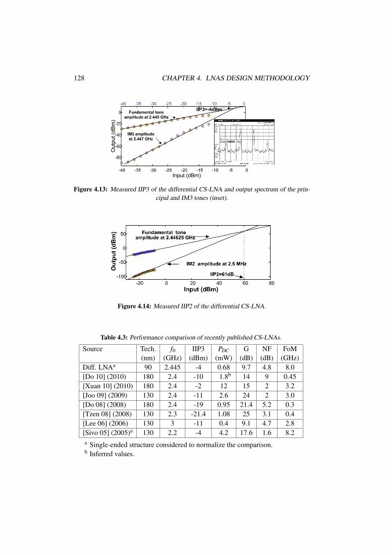
128 CHAPTER 4. LNAS DESIGN METHODOLOGY
Figure 4.13: Measured IIP3 of the differential CS-LNA and output spectrum of the prin-
cipal and IM3 tones (inset).
Figure 4.14: Measured IIP2 of the differential CS-LNA.
Table 4.3: Performance comparison of recently published CS-LNAs.
Source Tech. f0 IIP3 PDC G NF FoM
(nm) (GHz) (dBm) (mW) (dB) (dB) (GHz)
Diff. LNAa 90 2.445 -4 0.68 9.7 4.8 8.0
[Do 10] (2010) 180 2.4 -10 1.8b 14 9 0.45
[Xuan 10] (2010) 180 2.4 -2 12 15 2 3.2
[Joo 09] (2009) 130 2.4 -11 2.6 24 2 3.0
[Do 08] (2008) 180 2.4 -19 0.95 21.4 5.2 0.3
[Tzen 08] (2008) 130 2.3 -21.4 1.08 25 3.1 0.4
[Lee 06] (2006) 130 3 -11 0.4 9.1 4.7 2.8
[Sivo 05] (2005)a 130 2.2 -4 4.2 17.6 1.6 8.2
a Single-ended structure considered to normalize the comparison.b Inferred values.
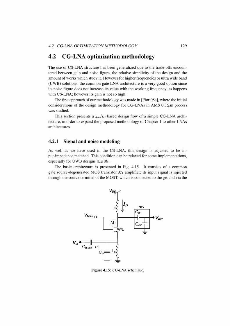
considerations of the design methodology for CG-LNAs in AMS 0.35
4.2. CG-LNA OPTIMIZATION METHODOLOGY 129
4.2 CG-LNA optimization methodology
The use of CS-LNA structure has been generalized due to the trade-offs encoun-
tered between gain and noise figure, the relative simplicity of the design and the
amount of works which study it. However for higher frequencies or ultra wide band
(UWB) solutions, the common gate LNA architecture is a very good option since
its noise figure does not increase its value with the working frequency, as happens
with CS-LNA; however its gain is not so high.
The first approach of our methodology was made in [Fior 08a], where the initial
μm process
was studied.
This section presents a gm/ID based design flow of a simple CG-LNA archi-
tecture, in order to expand the proposed methodology of Chapter 1 to other LNAs
architectures.
4.2.1 Signal and noise modeling
As well as we have used in the CS-LNA, this design is adjusted to be in-
put-impedance matched. This condition can be relaxed for some implementations,
especially for UWB designs [Lu 06].
The basic architecture is presented in Fig. 4.15. It consists of a common
gate source-degenerated MOS transistor M1 amplifier; its input signal is injected
through the source terminal of the MOST, which is connected to the ground via the
Figure 4.15: CG-LNA schematic.

130 CHAPTER 4. LNAS DESIGN METHODOLOGY
Figure 4.16: Small-signal scheme of the CG-LNA architecture studied.
Ls inductor. An external capacitor Cext is included to facilitate the input matching
condition with feasible low-value source inductor. Inductor Ld connects the supply
voltage to the drain terminal of M1 and the output network NW matches the load RLto the output impedance of the CG-LNA. The MOS transistor biasing is adjusted by
means of the DC gate voltage, which in this study it is considered an ideal source.
As a first approach, the inductor Ls is chosen to have a parasitic parallel resistance
at less ten times higher than the input source resistance, Rs, to neglect its effect in
the circuit.
To deduce the equations that govern this architecture, lets use the small-signal
schematic of Fig. 4.16, where capacitor Cgb does not appear as it is short-circuited.
The LNA is divided into two stages, the core stage and the output stage. The core
stage is composed by the MOS transistor M1, the inductor Ls and the external ca-
pacitor Cext . The output stage includes the core output impedance, Zo,MOS, where
Z−1o,MOS = R−1
o,MOS + jω0(Cgd +Cbd), the inductor Ld and its parasitic parallel resis-
tance R(p)ind,d . R
′L is the load seen from io.
Input stage analysis
The input matching condition is Zin = Rs + j0, hence computing Zin we have
Z−1in =
1
jω0Ls+ jω0(Cext +Cgs +Cgb)+
gm +gds
1+gdsR−1L
=1
Rs+ j0. (4.29)
From the real and imaginary part of the previous equality we obtain
R′L = Rs
(1+
gm
gds
)− 1
gds
Cext =1
ω20Ls
−Cgs −Cgb (4.30)
To reach the input matching condition, R′L, the load seen from io must be fixed to
the value expressed above.

4.2. CG-LNA OPTIMIZATION METHODOLOGY 131
The output parallel resistance of the input stage is
Ro,MOS = Rs
(1+
gm
gds
)+
1
gds. (4.31)
Output stage analysis
The output impedance Zout of the output stage is
Z−1out =
1
jω0Ld+
1
R(p)ind,d
+Z−1o,MOS
=1
jω0Ld+
1
R(p)ind,d
+R−1o,MOS + jω0(Cgd +Cbd)
= Gout + jBout (4.32)
where
Gout =1
R(p)ind,d
+1
Ro,MOS. (4.33)
Considering that the impedance seen at the input of the output network NW
must be Z∗out
−1 = Gout − jBout , the input impedance Z′L of the output stage is,
Z′L−1
=1
R′L
= jω0(Cgd +Cbd)+1
jω0Ld+
1
R(p)ind,d
+Gout − jBout (4.34)
The real and imaginary part of the previous expression are written as functions of
the unknown Gout , Bout and R(p)ind,d , as follows:
1
R′L
=1
R(p)ind,d
+Gout
Bout = ω0(Cgd +Cbd)+1
ω0Ld. (4.35)
As R′L is known from (4.30) we can write the unknowns Gout and R(p)
ind,d from (4.33)
and (4.35) as
Gout =1
2
( 1
Ro,MOS+
1
R′L
)(4.36)
1
R(p)ind,d
=1
2
( 1
R′L− 1
Ro,MOS
). (4.37)
If a capacitive output network NW is used, as we have explained in Sec-
tion 4.1.2, the following two conditions have to be met
Re(Zout) < RL, Im(Zout) > 0. (4.38)

132 CHAPTER 4. LNAS DESIGN METHODOLOGY
These conditions imply the following maximum value for the drain inductor:
Ld,max =1
ω0
(√Gout(1/RL −Gout)+ω0(Cgd +Cbd)
) (4.39)
Power gain
The power gain of the CG-LNA can be written as
G = 10log
(Pout
Pin
)= 10log
(i2o
4Gout/
v2s
4Rs
)(4.40)
As the transfer function of iin to io is the unity io = iin = vs/(2Rs), then
G = 10 log
(1
4RsGout
). (4.41)
Noise figure
The noise factor F of this architecture is
F = 1+(Fcore −1)+(FOS −1) =i2LNAcore,o
i2s,o+
i2Gout,o
i2s,o(4.42)
with i2s,o = (1/2)2i2s , as the function transference between is,o and is. Neglecting in
the expression of the psd of i2LNAcore,o the noise of the conductance gds and of the
induced gate noise, i2LNAcore,o∼= ind,o = ind|Δ( jω0)|2, with
Δ( jω0) =1
1+Rs(gm +gds)+gdsR′L
=1
2Rs(gm +gds). (4.43)
Finally
F =1+i2nd|Δ( jω0)|2
(1/2)2i2s+
i2Gout
(1/2)2i2s
=1+i2nd|Δ( jω0)|2
(1/4)i2s+4GoutRs = 1+
i2nd|Δ( jω0)|2(1/4)i2s
+10−G/10 (4.44)
where i2nd = 4kBT gmγα + KF g2
mC2
oxWL f , i2s = 4kBT/Rs and i2Gout = 4kBT Gout .
In this structure the effect of the gate noise is neglected respect to the other
noise components, even for frequencies up to ω0/ωT = 0.5 [Zhuo 05]. It is not the
case of a CS-LNA architecture, due to the input resonant tank that increases the
gate noise contribution by its quality factor. In case this noise would be added to
the equations, an interesting deduction is presented in [Lu 06].
4.2. CG-LNA OPTIMIZATION METHODOLOGY 133
4.2.2 Design methodology flowWith the resulting set of equations derived in the previous section, it is now possible
to lay-out a design flow, similar to the one proposed for the CS-LNA architecture,
as shown in Fig. 4.17. Again, the design flow covers the range of possible pairs
(gm/ID, ID), up to a maximum ID,max. For each pair, it is found the inductor Ls and
external capacitor Cext to reach the input impedance imaginary condition and Rextto adjust the input impedance real condition. Then it is calculated the power gain
G and the noise figure NF . The diagram flow follows the design steps listed below.
Step 1) Start by setting the constraints of a minimum transistor length Lmin and
the inductor LUT Λ(p)L , and the specifications: the working frequency f0,
the load RL, a maximum transistor bias current IDmax, a maximum noise
figure NFmax and and a minimum gain Gmin.
Step 2) Pick a pair of ID and gm/ID values, using the transistor technology
database, which is assumed previously collected.
Step 3) Find Ls included in Λ(p)L (see Section 2.3) whose Rp,s is much larger than
Rs, to limit the perturbation of the parasitic resistance of Ls over the input
impedance seen at the source of the MOST.
With the pair (gm/ID, ID), and the transistor technology database, pre-
sented in Chapter 2, obtain the corresponding normalized current i, the
gds/ID ratio and the C′i j.
Using the above data compute Cgs, Cgd , Cgb and Cbd . Calculate Cext and
R′L from (4.30), Ro,MOS from (4.31), Gout from (4.36), R(p)
ind,d from (4.37)
and Ld,max using(4.39).
Step 4) Find the inductor Ld included in Λ(p)L which inductance is lower than
Ld,max and parasitic parallel resistance equal to R(p)ind,d . If it does not exist
return to Step 2, otherwise continue.
Step 5) Compute the power gain and the noise figure using (4.41) and (4.44). If
NF > NFmax or G < Gmin, return to Step 2. Otherwise the flow is finished.
As it has been done in similar sections of the work, we have implemented this
design flow in MATLAB computational routines, making it possible to observe the
behavior of the design variables in contour maps. As initial values there have been
considered f0 = 2.445 GHz, Lmin=100 nm, Rs = RL=50Ω.
Figure 4.18.(a) presents the noise figure design space versus gm/ID and ID. It is
observed an optimum NF zone, along the line of the arrow. Also, for high currents,

134 CHAPTER 4. LNAS DESIGN METHODOLOGY
Figure 4.17: Design flow of the CG-LNA architecture.

4.2. CG-LNA OPTIMIZATION METHODOLOGY 135
Figure 4.18: (a) Noise figure (b) Power gain, (c) R′L and (d) Rp,d versus ID and gm/ID.

136 CHAPTER 4. LNAS DESIGN METHODOLOGY
the noise figure increases when moving to moderate and strong inversion, due to
the increment in the drain noise term of (4.42).
The power gain is plotted in Fig. 4.18.(b), which it is observed an increasing
tendency in the direction of the arrow; the power gain increases when moving to
weak inversion and when the bias current raises.
The behavior of resistor R′L is depicted in Fig. 4.18.(c); it is almost independent
of ID and increases when moving to weak inversion. A limit around 720 Ω exists
due to the maximum transistor width reachable. Moreover, the maps of Rp,d are
presented in Fig. 4.18.(d); this resistance increases with the bias current and when
moving to weak inversion.
4.3 ConclusionsThis chapter presents the third and four steps of our RF design methodology (ex-
posed in Chapter 1) for two topologies: CS-LNA and CG-LNA, for RF nanometer
technologies based on the gm/ID technique. The proposed methodology enables a
considerable design time reduction as little re-design is needed. It also shows the
design compromises of the LNAs, providing beforehand a complete panorama of
the LNA behavior when bias and inversion level is modified.
The study of the CS-LNA design space has been done by covering accept-
able current values and the MOS transistor parameter gm/ID, in order to study the
trade-offs of using different MOS transistor inversion levels in the design. Both
MOST and inductor data were extracted with SpectreRF simulations to accurately
and quickly model these components and include the database in the design flow.
The inclusion of the flicker noise in the noise figure computations is proven to be
needed in moderate and strong inversion zones. Rbias is added in the gain and noise
figure computation and it is shown their degradation when Rbias decreases. The
maps of noise figure, power gain, Ct and Ls versus the pair (gm/ID, ID) were dis-
played to see their behavior as the inversion level and bias current change. It has
been highlighted how designing in moderate inversion leads to a good compromise
of power reduction and acceptable noise figure and gain levels. Two application ex-
amples were implemented as a demonstrator of the presented method. Noise figure
and gain values obtained from mathematical computations following the method,
electrical simulations and measurements accord with each other with acceptable
error levels.
Finally, the architecture study and the design flow of the CG-LNA considering
real inductors is presented, to cover other LNA architectures in which the design
methodology presented in Chapter 1 can be applied.

4.A. APPENDIX A: CS-LNA ZO,MOS EXPRESSION 137
4.A Appendix A: CS-LNA Zo,MOS expressionThe output impedance of the CS-LNA Core Stage directly depends on the load seen
from the source of M2 to ground, which we call ZS2. This load includes the effect
of Rs, Lg, Cext , and M1 transistor transconductance gm, gds, Cgs and Cgd . As in the
rest of the work, M1 is considered identical to M2. The small-signal schematic of
Fig. 4.19 is used to obtain Zo,MOS. For this study, capacitor Cgd has been considered
as its feedback changes the output impedance, especially for MOST with large
widths.
To compute ZS2, it is considered two impedances: 1) ZG1, the impedance seen
from the gate of M1 to the input (which is grounded); and 2) Zvin, the impedance
seen from the gate of M1. Then, ZG1 is
ZG1 = (Rg +Rs)+ sLg, (4.45)
and Zvin is
Zvin =vg1
it≈ sLs +
1
sCt+Ls
gm
Ct. (4.46)
From these equations, ZS2 is
ZS2 ≈1
sCgd+ ZvinZG1
Zvin+ZG1
1+ gmZG1
sCt(Zvin+ZG1)
(4.47)
Then Zo,MOS has the following expression
Zo,MOS ≈ 1+(gm + sCgs)ZS2
gds + sCgd(1+(gm + sCgs)ZS2). (4.48)
Figure 4.19: Schematic used to calculate CS-LNA Zo,MOS.


CHAPTER 5
Design Methodology Applications ina Complex System
THE IMPLEMENTATION OF a low-power 2.4-GHz ZigBee transceiver is
one of the goals of the main project in which this thesis has been embed-
ded. To reach this objective, intermediate steps were performed to test
the possible architectures of the involved blocks. This chapter presents
the implementations of some RF preliminary blocks where our developed design
methodology (or part of it) has been used. It also introduces the final ZigBee trans-
ceiver analog front-end.
The list of circuits begins with the implementation of a single-ended-input RF
receiver front-end, presented in [Fior 11c]. With this block we aimed to check
the pros and cons of using a single-ended input instead of a differential one. This
front-end utilizes a single-ended CS-LNA, designed under the design methodology
studied in Chapter 4. We deduce the front-end and CS-LNA specifications from
the ZigBee requirements presented in [Vill 07]. The same CS-LNA was fabricated
as a separate block in order to test it individually. Section 5.1 introduces the imple-
mented circuits as well as their simulation and measurement results
The referred project also includes the study and design of built-in self-test
(BIST) of RF circuits. We use a modified version of the previous single-ended
CS-LNA to implement a demonstrator of a BIST technique using an on-chip en-
velope detector, which we present in [Barr 11a, Barr 11b] and we describe in Sec-
tion 5.2. This dissertation only provides a brief discussion concerning the adjust-
ments done in the LNA as well as the measurements of the on-chip demonstrator.
The transmitter front-end of the ZigBee transceiver needs a power amplifier
(PA) to deliver the required power to the antenna. We designed a Class C PA, based
on the design methodology we presented together with Barabino in [Bara 10]. That
methodology considers the characterization techniques of MOST and passive com-
ponents presented in Chapter 2, using them for describing a large-signal circuit
behavior. In Section 5.3 PA measurements are provided.
Finally, an overview of the design of the ZigBee transceiver analog front-end is
introduced in Section 5.4. For this design two new LNA and PA circuits with new
specifications were designed, reflecting the fact of the reduction in the design time
from specifications to layout, once computational routines are developed.
139

140 CHAPTER 5. DESIGN METH. APPLICATIONS IN A COMPLEX SYSTEM
5.1 Single-ended input 2.4-GHz ZigBee receiverfront-end
To study the feasibility of utilizing a single-ended input LNA in the ZigBee re-
ceiver, it has been designed a single-ended input differential-output RF front-end,
which was presented in [Fior 11c]. It consists of a single-ended CS-LNA, AC cou-
pled to a differential switched transconductor mixer (SW-MIX) [Klum 04], which
schematic is shown in Fig. 5.1. We consider the possible use of a single-ended LNA
since it enables 1) discarding the use of an input balun or a differential antenna, 2)
reducing to half the power consumption of the block as there is only one LNA
branch, and 3) reducing the silicon area. However, the second order intermodula-
tion increases respect to a differential LNA. For our design, acceptable results in
terms of linearity are observed, as the IIP2 exceeds the 10.5 dBm [Oh 05] which are
expected in a ZigBee receiver. As the whole receiver was planned to work under a
low-IF scheme, we implemented this structure accordingly. The used intermediate
frequency was 2.5 MHz, to reduce the flicker noise effects and to achieve a good
trade-off with the specifications of the baseband circuits at the receiver back-end as
well as to simplify the PLL frequency division since an integer divider is required.
The LNA has two-gain modes: high gain mode (hg) is used when low signal levels
arrive to the system; low gain mode (lg) is applied when high input signals at the
mixer input can cause signal compression due to the mixer non-linearities.
As the structure was used to evaluate the single-ended alternative, we discarded
the use of packaging for test. Instead the front-end has been designed to be tested
with microprobes. The LNA and the mixer were designed separately to be tested
individually. As all the RF equipment of our laboratory is single-ended and has
50 Ω-input impedance, the single-ended input of the CS-LNA and each of the
LO inputs of the SW-MIX (where the external clock is injected) as well as the
output of the CS-LNA and the inputs of the SW-MIX were all matched to 50 Ω, as
Fig. 5.1.(b) depicts. At the output of the SW-MIX, an external buffer is placed to
enable the 50-Ω input impedances of the Spectrum Analyzer or the Noise Figure
Analyzer connectors.
LNA and mixer were biased to work in moderate-weak inversion region in order
to minimize the power consumption and also to enable the possibility of reducing
the supply voltage, especially due to differential transconductor mixer architecture
used.
The ZigBee receiver, and hence, the front-end, were specified to work in the
2.4 GHz-2.5 GHz band with a supply voltage of 1.2 V. The specifications of voltage
conversion gain CGV , noise figure NF , IIP3 and P1dB are listed in Table 5.1. These
data are obtained by considering the ZigBee standard requirements and the other
chain blocks of the receiver as presented in [Vill 07]. The noise figure specification
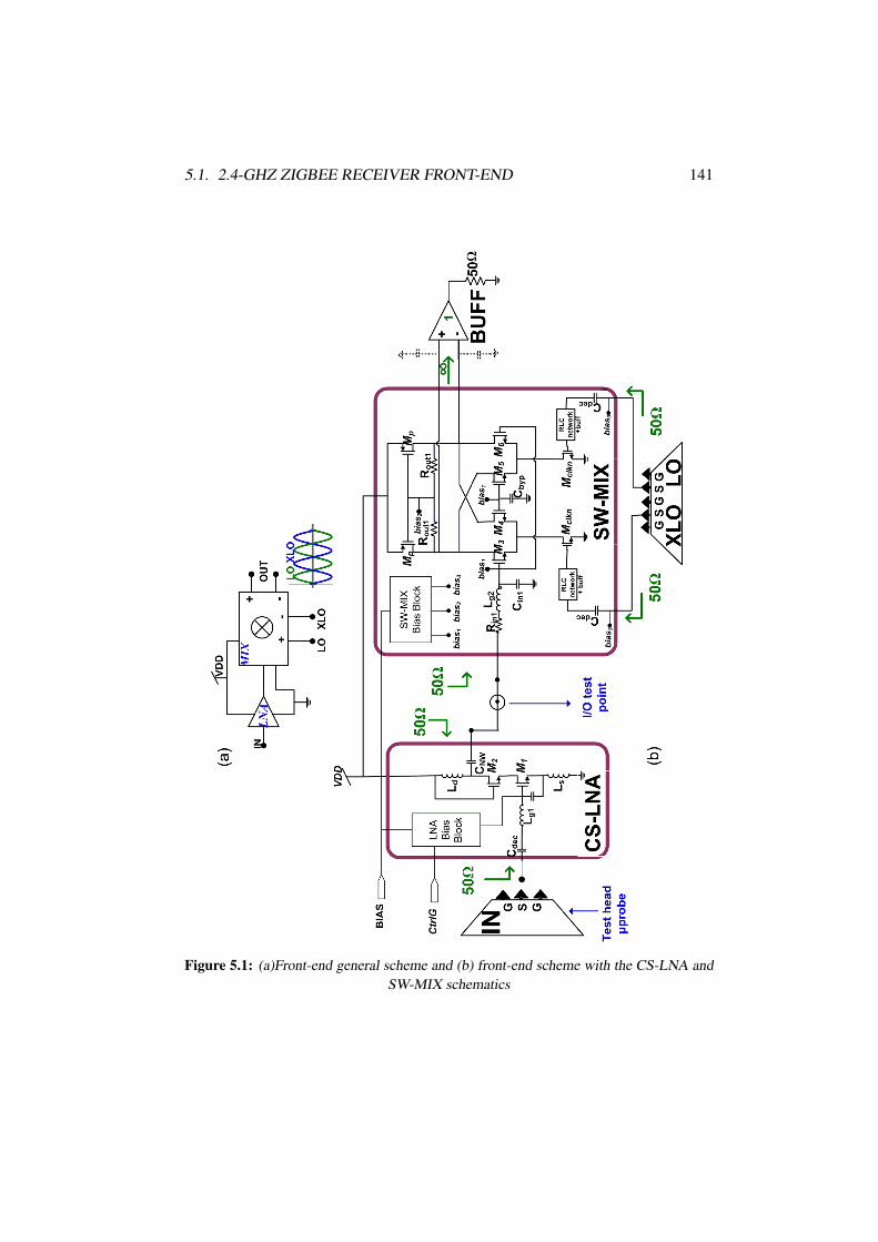
5.1. 2.4-GHZ ZIGBEE RECEIVER FRONT-END 141
Figure 5.1: (a)Front-end general scheme and (b) front-end scheme with the CS-LNA and
SW-MIX schematics

142 CHAPTER 5. DESIGN METH. APPLICATIONS IN A COMPLEX SYSTEM
Parameter Total Front-End CS-LNA SW-MIX
CGV (dB) >25 >10 >15
NFhg (dB) <12 <5 <15
P1dBlg (dBm) >-23 >-10 >-15
IIP3lg (dBm) >-13 >0 >-5
Table 5.1: Front-end specifications.
is given for the hg mode of the LNA, since in this mode the input signals are lower
and are more affected by the intrinsic noise of the device. The opposite situation
happens with the 1dB compression point, P1dB, and the IIP3 characteristics, which
are specified for lg mode, since the system is more demanded in terms of linearity
when high input signals arrive, and hence, when the LNA is set to lg mode.
The LNA design will be detailed in next section (Section 5.1.1). The
SW-MIXER has been designed by other member of the research group, so it is
not part of this thesis and hence it is not discussed here. Only for presenting a gen-
eral panorama, the specifications of the mixer and its achieved features are listed
in Table. 5.2. A complete discussion of this design can be found in the works of
[Vill 10] and [Fior 11c].
The front-end final layout is presented in Fig. 5.2; it has an area of 0.74 mm2,
which 45% of this area is ocupied by the SW-MIX. As two-third of the mixer area
is occupied by the matching network inductors of the LO ports and of one of the
input matching network inductor -whose input is grounded-, the effective area of
the front-end is 0.52 mm2.
Table 5.3 presents the post-layout simulated results and the measurements of
the fabricated front-end. The results of the post-layout simulations cover the spec-
ifications of Table. 5.1. We provide the NF for 2.5 MHz and 10 MHz because our
specific equipment for noise figure measurements, the Agilent E4440A Spectrum
Parameter CS-LNA CS-LNA SW-MIX SW-MIX
Specs. Post-layout Specs Post-layout
CGV (dB) >10 12.4/9 >15 20
NFhg (dB) <5 3.7 (hg) <17 15.1
IIP3lg (dBm) >0 -1.2 >-5 -3.5
P(mW) lowest 1.44/0.92a lowest 3.24/5.9b
a hg/lg modesb Inferred from the total measured current of 6.9/6.47 mA (hg/lg)
minus the simulated current of 3.0 mA of the first level clock
buffers.
Table 5.2: CS-LNA and SW-MIX specifications and post-layout simulations.

5.1. 2.4-GHZ ZIGBEE RECEIVER FRONT-END 143
Figure 5.2: Front-end microphotograph.
Analyzer, only reaches frequencies down to 10 MHz; for frequencies lower than
10 MHz the NF measurements were made with the Agilent N8974A Noise Figure
Analyzer. The conversion gain was measured with the Spectrum Analyzer in the
0.5 MHz-16 MHz band. Post-layout simulated results and measurements of the NF
and CG are presented in Fig. 5.3.(a) and (b). Differences in the CG are expected
since the model of the mixer load is not very accurate.
Finally the in-band test of IIP3, measured with two-tone input signal, fRF1,2 =fLO ± fIF ± 0.3MHz, with fLO=2.445 GHz and fIF=2.5 MHz, is shown in
Fig. 5.4.(a), with an extrapolated IIP3 of -12.8 dBm. The P1dB in hg mode is
around -26 dBm, then, giving a security margin of 4 dB, we infer that the hg mode
should be used up to -30 dBm. Above it and up to -20 dBm, the LNA should switch
to lg mode. Fig. 5.4.(b) presents the output spectrum for a -35 dBm OQPSK input
signal.
With the FoM of [ITRS 09] (see (4.28)), a list of active front-end circuits is
presented in Table 5.4. Very good results are obtained, especially compared with
the most recently reported, as [Nguy 10, Zito 09]. The work of Liscidini, [Lisc 05],
Table 5.3: Front-end post-layout simulations and measurements.
Parameter Post-layout Sim. Measurement
Current (hg/lg) (mA) 3.9/3.47 3.9/3.47
CGV @ 2.5MHz (hg/lg) (dB) 32.5/30 30/28
NF @ 2.5MHz (hg) (dB) 8.5 7.5
NF @ 2.5MHz (lg) (dB) 9.3 9.6
IIP3 (hg) (dBm) -12.8 -16.2 ± 1.0
IIP3 (lg) (dBm) -9.8 -12.8 ± 1.5
IIP2 (hg) (dBm) - 14.4 ± 1.0
Zin @ 2.445GHz (Ω) 44.7 47
S11 of In port @ 2.445GHz (dB) -24 -21

144 CHAPTER 5. DESIGN METH. APPLICATIONS IN A COMPLEX SYSTEM
Figure 5.3: Comparison of measured versus simulated (a) NF and (b) CG of the front-end
(hg case) for a -35dBm input.
Figure 5.4: (a) Measured IIP3 for the low gain case and (b) front-end output spectrum of
a -35dBm OQPSK input signal.

5.1. 2.4-GHZ ZIGBEE RECEIVER FRONT-END 145
has better FoM due to its low noise figure, but its very high power consumption is
not very suitable for ZigBee applications.
As conclusions, a single-ended input front-end for low power, suitable for Zig-
Bee has been designed. The use of a single ended input CS-LNA reduces power,
area and external chip components. The operation of MOS transistor in moder-
ate and weak inversion regions helps to reduce power and supply voltage. Finally
good FoM has been achieved compared with other ZigBee front-ends designs. The
linearity of the block is acceptable for a ZigBee receiver.

146 CHAPTER 5. DESIGN METH. APPLICATIONS IN A COMPLEX SYSTEM
Tabl
e5.
4:C
om
pari
son
betw
een
the
desi
gned
front-
end
(F-E
)and
oth
er
publi
shed
work
s.
Ref
.te
ch.
CG
(dB
)N
F(dB
)II
P3(d
Bm
)Po
wer
(mW
)f 0
(GH
z)Fo
M(M
Hz)
Obs
.F
-Elg
90nm
28
9.6
-12.8
4.6
82.4
45
95.4
-
F-E
hg90nm
30
7.5
-16.2
4.6
82.4
45
85.7
IIP
2=
14.4
dB
m
[Nguy
10]
180nm
22
9-1
55.4
2.4
45
25.9
dual
band
[Zit
o09]
SiG
e350nm
26
8.7
-13
8.6
2.4
45
44.3
-
[Song
06]
180nm
31.5
11.8
NA
0.5
2.4
-N
F@
10M
Hz
[Jarv
05]
130nm
14.5
24.5
-21
1.6
82.4
45
0.2
out-
of-
band
IIP
3
[Kw
on
05]
180nm
19
11
-94.2
52.4
45
55.7
IF=
480
MH
z
[Lis
c05]
130nm
23.4
5.8
-4.8
24
2.3
167.5
802.1
1b-g
[Beff
02]
180nm
21.4
13.9
-10
6.4
82.4
45
18.8
IF=
2M
Hz

μm
(dBm)
5.1. 2.4-GHZ ZIGBEE RECEIVER FRONT-END 147
5.1.1 Single-ended CS-LNA designThe single-ended CS-LNA of the front-end previously described was implemented
in a stand-alone version to verify the proposed methodology and to demonstrate a
BIST stragegy for RF blocks, which will be described in Section 5.2.
The implemented CS-LNA schematic is seen in Fig. 5.1.(b). We follow the
LNA design methodology presented in Chapter 4 to obtain this LNA design. In
this chip, the silicon area was a strong constraint, so the maximum value of the
MOS transistor bias resistance, Rbias, (already presented in Chapter 4) was limited
again to 1 kΩ, in the same way as happened with the differential CS-LNA design of
Section 4.1.5. Table. 5.5 presents the results of the computed design (under nomi-
nal conditions, with hg mode), the simulated schematic and the layout simulations.
In lg mode, the current drops down to 0.8 mA, the post-layout gain moves to 9 dB
and the IIP3 raises to -1.24 dB, consuming 0.92 mW, while in hg mode it increases
up to 1.44 mW for a 1.2 V power supply.
The microphotograph of the single-ended LNA is shown in Fig. 5.9.(a), where
all the components and blocks are highlighted.
LNA measured S-parameter are shown in Fig. 5.5. The frequency range of the
measurements includes the ZigBee band of 2.4 GHz-2.5 GHz. The measurement
set-up is the same as the one used for the differential CS-LNA of Section 4.1.5. The
input network is centered at 2.42 GHz, in the band of interest (|S11| ≤ −20 dB).
The output network resonant frequency has a shift of 150 MHz down, visualized
when trace |S22| minimizes at 2.3 GHz (|S22| < −20 dB), which again affects the
gain and the NF responses, shift down their maximums and minimums. It also has
Characteristics Calc. Sim. Post-layout
ID (mA) 1.2 1.2 1.21
gm/ID (V−1) 17 17 17
Ls (nH) 0.8 0.8 1.1
Lg (nH) 7.9 7.9 9.8
Ld (nH) 9.4 7.1 7.1
WM1( ) 165 165 157
Cgs (fF) 158 150 151
Cext (fF) 207 200 141
G (dB)Rbias=10kΩ 15.4 14.5 -
Rbias=1kΩ 14.4 13.0 12.5
NF (dB)Rbias=10kΩ 1.9 2.3 -
Rbias=1kΩ 3.0 3.6 3.7
IIP3 -5.2 -4.4
Table 5.5: Single-ended CS-LNA component values comparison between Matlab and
Spectre RF simulations.
-
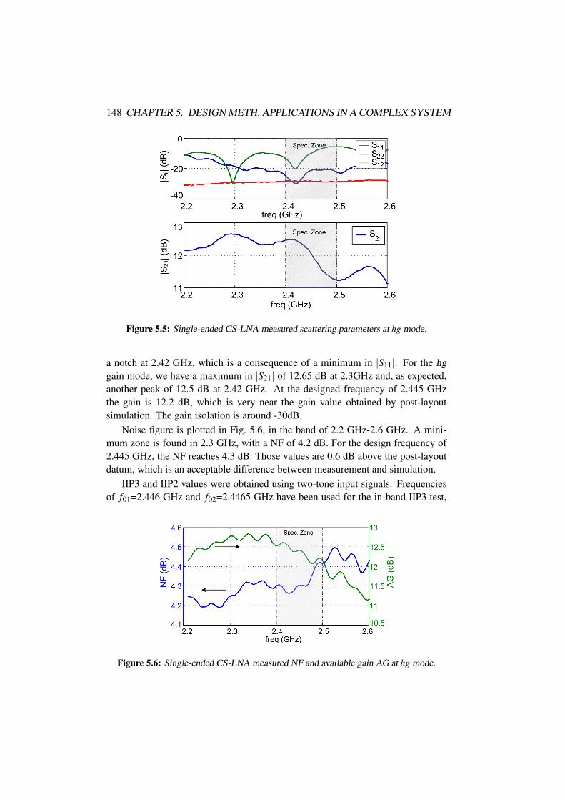
148 CHAPTER 5. DESIGN METH. APPLICATIONS IN A COMPLEX SYSTEM
Figure 5.5: Single-ended CS-LNA measured scattering parameters at hg mode.
a notch at 2.42 GHz, which is a consequence of a minimum in |S11|. For the hg
gain mode, we have a maximum in |S21| of 12.65 dB at 2.3GHz and, as expected,
another peak of 12.5 dB at 2.42 GHz. At the designed frequency of 2.445 GHz
the gain is 12.2 dB, which is very near the gain value obtained by post-layout
simulation. The gain isolation is around -30dB.
Noise figure is plotted in Fig. 5.6, in the band of 2.2 GHz-2.6 GHz. A mini-
mum zone is found in 2.3 GHz, with a NF of 4.2 dB. For the design frequency of
2.445 GHz, the NF reaches 4.3 dB. Those values are 0.6 dB above the post-layout
datum, which is an acceptable difference between measurement and simulation.
IIP3 and IIP2 values were obtained using two-tone input signals. Frequencies
of f01=2.446 GHz and f02=2.4465 GHz have been used for the in-band IIP3 test,
Figure 5.6: Single-ended CS-LNA measured NF and available gain AG at hg mode.

5.1. 2.4-GHZ ZIGBEE RECEIVER FRONT-END 149
Figure 5.7: Measured (a) IIP3, (b) P1dB and (c) IIP2 of the single-ended LNA at hg mode.
with a measured output frequency of 2.4455 GHz. As Fig. 5.7.(a) stands, the mea-
sured IIP3 is -3.4 dBm for the hg mode. We also measure the 1dB compression
point P1dB, with the network analyzer, as seen in Fig. 5.7.(b); the gain falls 1 dB
when the input power is -11.5 dBm. The IIP2 measurement data are shown in
Fig. 5.7.(c). Similarly, an IIP2 two-tone test with frequencies of f01=2.445 GHz
and f02=2.445 GHz+2.5 MHz, have been used; doing the intermodulation, the spur
falls in the 2.5 MHz IF band. The measured value was 29.5 dBm, a very good value
considering the single-ended architecture and the lack of internal calibration.

150 CHAPTER 5. DESIGN METH. APPLICATIONS IN A COMPLEX SYSTEM
5.2 Demonstrator for an RF BIST methodologyThis section presents the RF Built-in Self Test (BIST) demonstrator which validates
the methodology for testing embedded LNA we presented in [Barr 11a]. It is based
on the detection and analysis of the response envelope to a two-tone input signals
of an RF block, e.g. an LNA. The description of this methodology, out of the scope
of this work, is fully discussed in [Barr 11a] where we showed the feasibility of
coupling the envelope detector to an LNA output. A slightly modified version of
the LNA included in the receiver front-end exposed in Section 5.1.1 has been used
as a part of this demonstrator, just adjusting the LNA output network to match
the whole design to 50 Ω. The schematic is visualized in Fig. 5.8. The layout is
depicted in Fig. 5.9. We have used the envelope detector architecture presented
in [Cha 09], which comprises a voltage-to-current converter and an AC-coupled
half-wave current-mode rectifier with a passive low-pass filter.
The simulated results of the CS-LNA characteristics with and without the en-
velope detector and the measurements are listed in Table 5.6. No appreciable
variations are observed among the simulated characteristics of the block with and
without the envelope detector. For the measured results, the NF differs from the
simulated characteristics in 0.5 dB, which is an acceptable spread for noise figure
measurements. The measured input waveform of the envelope detector (output of
the CS-LNA) and output of the envelope detector, obtained with the Oscilloscope
DSO81304B Infiniium of Agilent, are presented in Fig. 5.10. As it is expected, the
output signal follows the envelope of the input signal.
This single-ended CS-LNA has also been used as a demonstrator of the RF
alternate test using multi-VDD conditions method we presented in [Barr 11b].
Figure 5.8: Schematic of the CS-LNA with the envelope detector.

5.2. DEMONSTRATOR FOR AN RF BIST METHODOLOGY 151
Table 5.6: CS-LNA characteristics measured and simulated with and without envelope
detector.
Specification LNA without LNA with codesigned Measured with
envelope detector envelope detector envelope detector
Gain (dB) 12.5 12.4 12.3
NF (dB) 3.66 3.66 4.25
IIP3 (dBm) -4.4 -3.5 -4
CP1dB (dBm) -15 -15.1 -12.5
S11 (dB) -24.8 -25.2 -21.1
S22 (dB) -9.8 -11.3 -11.2
S12 (dB) -26.4 -26.5 -28.2
Figure 5.9: (a) Microphotograph of the single-ended CS-LNA with the Envelope Detector
where active area and passive components are highlighted. (b) Single-ended CS-LNA with
the Envelope Detector measurement set-up.
Figure 5.10: Measured input signal of the envelope detector (in magenta) and output of
the envelope detector (in green).

152 CHAPTER 5. DESIGN METH. APPLICATIONS IN A COMPLEX SYSTEM
5.3 Class-C PA design
The ZigBee transceiver needs a power amplifier (PA) that provides the required
power to the antenna. We have designed a PA [Fior 10] following the Classes A-
AB-C PA design methodology we presented in [Bara 10]. In this methodology
we apply similar ideas the one presented in the general design methodology of
Chapter 1, but in a large-signal design. In this method: 1) the DC behavior MOS
transistor and the passive component are equally modeled, 2) the PA is described
by means of a set of large-signal expressions and 4) a design flow, which uses items
1), 2) and 3) is developed. The PA described in this section reasserts the validity
of working with semi-empirical device models in RF circuits. Furthermore, as
presented in [Bara 10], it shows that this validity is extended to a design with the
MOS transistor operating in a non-linear large-signal mode as it is the case of
Class C PAs.
As Class C PAs supports phase modulations they can be used in a ZigBee im-
plementation. A differential topology was designed and fabricated, despite the
method is developed for a single-ended scheme. The PA was implemented in the
TECH1 technology, having all the inductors on-chip. The scheme used is presented
in Fig. 5.11, where the differential source and load impedances are real and equal
to 100 Ω. The PA consists of an active block (MOS transistor M1) and an output
network (Lout , Cout1, Cout2 and Rbias); the input network is used to couple the input
signal (coming from a 50 Ω RF signal generator) to the gate of the transistor M1,
the effective PA input.
Figure 5.11: Schematic of the designed PA: (a) differential scheme (b) single ended view.

5.3. CLASS-C PA DESIGN 153
The PA design flow sets a group of PA specifications (output power of the fun-
damental tone Pout , second and third harmonic output power, P2nd
harm and P3rd
harm and
power efficiency η) and fixes two boundary conditions: 1) to give the maximum
power to RL, the maximum voltage swing at the drain voltage must be fixed to
[0,2VDD], and 2) the MOS transistor minimum length Lmin to reach high fT . With
the specifications and the boundary conditions, the design flow of [Bara 10] is ap-
plied, obtaining a final design where the transistor width, the output network sizing,
the DC gate voltage vDCG and the maximum amplitude at the gate vRF
G are set.
The PA design flow of [Bara 10] is briefly resumed below. To implement it, the
data of Chapter 2 is previously needed: 1) MOS transistor LUTs, and 2) inductors
LUT. The design flow is:
Step 1) Due to filtering of the output network: 1) the voltage signal at the drain of
M1 is almost sinusoidal and the peak value is almost VDD (if the DC drain
voltage is fixed to VDD and 2) the load resistance RL is transformed to a
resistance seen from the drain, RNW . Then, calculate RNW ∼= 1/2V 2DD/Pout .
Step 2) Choose a pair of values for the DC gate voltage and the RF peak gate
voltage, which sum does not surpass VDD and subtraction is above zero.
Step 3) The two main hypothesis of [Bara 10] are: 1) the normalized drain current
in each time interval, for a whole period, is obtained by using the normal-
ized current i, considering that the gate and drain voltages of the MOS
transistor LUT are the instantaneous gate and drain voltages, (considering
no difference of phase between the instantaneous drain and gate voltages;
and 2) the MOST is working under the quasi-static condition.
With these hypothesis, find the normalized drain current in the time do-
main, as well as its DC, fundamental, second and third harmonic (IDC, I1,
I2, I3), applying Fourier expansion.
Step 4) Calculate the MOS transistor efficiency ηMOS with ηMOS ∼= I1/2IDC.
Step 5) Calculate the output network efficiency ηNW with ηNW = 1−RNW /Rp,ind ,
being Rp,ind the parasitic resistance of the inductor. Calculate the total
power efficiency of the PA as η = ηMOSηNW .
Step 6) Calculate the MOST aspect ratio as W/L = 2PNW /(VDDI1), being PNWthe delivered power to the network, calculated as PNW = I1VDD/2 =V 2
DD/(2RNW ).
This methodology has been implemented in a set of MATLAB computational
routines by Barabino. It generates maps of efficiency, transistor width and output
inductor versus the pair of DC gate and signal gate voltages. The efficiency map is
shown in Fig. 5.12.

154 CHAPTER 5. DESIGN METH. APPLICATIONS IN A COMPLEX SYSTEM
Figure 5.12: Efficiency contours versus DC gate and signal gate voltage pair (V DCG ,V RF
G ).
5.3.1 PA implementationWith the design flow and the computational routines, we design in TECH1 a
Class-C PA, suitable for 2.4 GHz ZigBee transmitters. A summary of specifica-
tions is provided in Table. 5.7. This PA uses 1.2 V MOS transistor, so the VDDcould reach up to 0.65 V. The final design point chosen is a DC gate voltage of
0.5 V and a gate peak voltage of 0.4 V and an efficiency of 51.2% as shown in
Fig. 5.12. The transistor width is 42.2 μm and the output network is: Lout=5.64 nH,
Cout1=1.57 pF and Cout2=0.69 pF. The post-layout simulation results of the imple-
mented circuit is listed in Table 5.8. The microphotograph of the PA is visualized
in Fig. 5.13.
Pout ≥ 0 dBm RL = 100Ω VDD = 0.65VV RF
D = 0.6V Rp,ind > 1kΩ P2ndharm ≤−40 dBc
P3rdharm ≤−20 dBc η > 35% OP1dB=-10 dBm
Table 5.7: Summary of the chosen PA specifications.
Figure 5.13: Microphotograph of the designed PA

5.3. CLASS-C PA DESIGN 155
Characteristics Post-layout sims. Characteristics Post-layout sims.
VDD 0.65 V Gpow 26 dB
PDC 3.16 mW ID 4.6 mA
η 46.6 % P2nd
harm -67 dBc
Pout 1.9 dBm P3rd
harm -21 dBc
Table 5.8: PA characteristics of SpectreRF post-layout results for a input power at the input
network of -2.5 dBm.
Figure 5.14: Measured PA efficiency and power added efficiency PAE.
The chip has been partially measured, and first results of differential efficiency
and output power are presented in Figs. 5.14 and 5.15. The PA reaches efficiencies
of 46% for input powers of -22 dBm. The 1 dB output power compression point
OP1dB is -5dBm. The input power of the active block has been inferred from the
22.5dB of expected losses of the input network.
In Fig. 5.15.(b) a plot of the output power spectrum due to an input injected
signal of -2.5 dBm and an inferred signal of -25 dBm at the input of the PA, is
shown. The fundamental power was around -1 dBm (after cable loss corrections).
The second harmonic has a value around -25 dBc and the third harmonic around
-36 dBc. There is a variation in the second and third harmonics respect to the
expected simulated values. It is due to the unbalanced output paths which cause
this effect.

156 CHAPTER 5. DESIGN METH. APPLICATIONS IN A COMPLEX SYSTEM
Figure 5.15: (a)PA measured output power versus the inferred input power injected at
the gate. (b) Measured output full spectrum of the PA for an input signal of -2.5dBm (no
correction due to the set-up losses are applied).
Figure 5.16: PA output spectrum of an OQPSK modulated input signal (no correction due
to the set-up losses are applied).
Finally the output spectrum of OQPSK with a signal bandwidth of 2 MHz is
depicted in Fig. 5.16.
To conclude, a compatible IEEE 802.15.4 Class C PA design in 90nm CMOS is
presented. It is based on the “Design efficiency approach” presented in [Bara 10].
Post layout results and preliminary measurements show very good agreement with
MATLAB results. Preliminary measurement simulation results show similar re-
sults in term of efficiency and output power.

5.4. DESIGNED BLOCKS IN A ZIGBEE ANALOG TRANSCEIVER 157
was preferred to reject that noise, hence the single-ended LNA architecture already
studied was discarded.
As the LNA and the PA for the analog transceiver were specified with a new
set of values, two new designs for these blocks were done utilizing their already
presented design methodologies. The designed LNA, at 2.445 GHz has a differen-
tial input impedance of 100 Ω and a differential output impedance of only 50 Ω,
a voltage gain of 6 dB, a noise figure of 4.5 dB, an IIP3 of -7 dBm and a power
consumption of 900 μA. The gain is lower than the differential design presented in
Chapter 4 because the current is lower and the maximum Ld , and hence, the maxi-
mum Rind,p were lower due to the reduction in the single-ended load RL from 50 Ωto 25 Ω.
The PA has been designed with 2.5 V-MOS transistors to use a VDD of 1.2 V
and to permit the MOS drain to have a maximum output excursion of 2.4 V. The M1
transistor length is 280 nm (the minimum available for these MOS transistors) and
its width is 104 μm. The final design point was: DC gate voltage V DCG =0.61 V and
gate voltage amplitude V RFG =0.34 V, for each single-ended input. Its maximum DC
power consumption is 3.7 mW, the output power reaches 2.5 dBm for a 100 Ω load,
with an output P1dB of 0 dB, and an efficiency of 24 %. This fall in the efficiency
of this PA respect to the one designed is due to the higher transistor lengh and the
value of the maximum amplitude at its input, given by the up-conversion mixer.
Experimental results shown the correct operation of the receiver-transmitter
system using two PCBs (Fig. 5.19), one with the chip acting as receiver and the
other as transmitter. When an OQPSK baseband signal is injected at the trans-
mitter baseband inputs, the output receiver signal after demodulation is shown in
Fig. 5.20.(a) and the modulated OQPSK spectrum captured with the Spectrum An-
alyzer is presented in Fig. 5.20.(b).
5.4 Designed blocks in a ZigBee analog transceiver
This thesis work finished with the description of the design of a low-power
2.4-GHz ZigBee transceiver, which block diagram and microphotograph are shown
in Fig. 5.17 and Fig. 5.18. We take part in the design of the LNA and the PA. In
this ZigBee transceiver, a VCO was designed following a different approach that of
resented in this thesis, by another designer of the group. The receiver and the trans-
mitter architectures were fully-differential, so as the LNA and PA blocks. Due to
lack of substrate models to emulate the amount of digital noise that reaches the RF
blocks -generated principally by the PLL-, a differential scheme for all RF blocks

158 CHAPTER 5. DESIGN METH. APPLICATIONS IN A COMPLEX SYSTEM
Figure 5.17: Transceiver block diagram
Figure 5.18: Transceiver microphotography and sub-block and signaling distribution.
Figure 5.19: Boards used in the transmission-reception experiment.

5.4. DESIGNED BLOCKS IN A ZIGBEE ANALOG TRANSCEIVER 159
Figure 5.20: Transmission-reception experiment: (a) eye diagram of the demodulated re-
ceiver output of a ZigBee beacon frame and (b) transmission verification using a Spectrum
analyzer, the inner image shows the modulated OQPSK spectrum.

160 CHAPTER 5. DESIGN METH. APPLICATIONS IN A COMPLEX SYSTEM
5.5 ConclusionsThis chapter presents the final design of the complete analog ZigBee transceiver as
well as the realization of a set of circuits implemented in previous stages. Only the
overview of the final PA and LNA blocks implemented in the ZigBee transceiver
was presented. All circuits designed followed the methodology of Chapter 1 or
a modified version considering MOS transistor large-signal operation, as it is the
case of the implemented PAs. Finally, the reuse of LNA and PA computational
routines and technology LUT allow an effective reduction of design time.

CHAPTER 6
Conclusions and Future Lines
6.1 Thesis conclusions
• It has been developed a design methodology for analog radiofrequency
blocks, focused to nanometer technologies and based on the transistor mod-
eling in all-inversion regions.
• The design methodology easily presents the trade-offs involved in each par-
ticular design and the consequences of modifying the parameters of the RF
block. It is noticed the reduction of design time when applying the method-
ology, as little adjustments are needed after the election of the design point, a
fact proven in the designed circuits by electrical simulations and experimen-
tal implementation.
• It has been demonstrated the utility of the gm/ID tool in the RF design, by
systematically covering all-inversion regions of the MOS transistor and by
exploiting the MOS transistor potential and the performance trade-offs of the
RF block.
• It has been validated the use of MOS transistor semi-empirical models based
on the small-signal characteristics of the device: the transconductance over
drain current ratio, gm/ID, versus the normalized current i, the conductance
gds, the five capacitance of the quasistatic model and the noise parameters.
• The quasistatic limit of one tenth of the transition frequency, used to re-
duce the number of capacitances involved and to simplify the MOS transis-
tor study, proves to be valid in the considered designs. Acceptable results are
also obtained when working a bit beyond that limit.
• It has been proven the validity of RF passive devices simplified models, ob-
tained by means of AC simulation at the working frequencies assumed.
• MOS transistor and passive devices modeling proves to be very efficient as
the data is collected once and reutilized for all the circuits and design flows.
161

162 CHAPTER 6. CONCLUSIONS AND FUTURE LINES
• It has been shown that for the implemented RF circuits, integrated in
nanometer technologies, the best performance compromises generally oc-
curs in the MOS transistor moderate inversion region. Good agreement ex-
ists between measurements on implemented designs and the values derived
from the design flows.
• Specific design methodologies were derived for LNAs and LC-VCOs archi-
tectures.
It has been considered the MOS transistor drain noise and flicker noise in
all-inversion regions.
• In the LC-VCO, it has been studied the design compromises due to the in-
version region and the tank inductor value. It is seen how designing in mod-
erate/weak inversion leads to a consumption reduction and a phase noise
increment; on the other hand reducing tank inductor values contributes to an
improvement in the VCO spectral purity.
It has been presented an LC-VCO phase noise model, based on the Hajimiri’s
model, for all-inversion region of the MOS transistor.
• The LNA performance study has been done varying the inversion level and
the drain current of the MOS transistor. It is shown the good trade-offs ob-
tained when working in moderate/weak inversion regions in terms of noise
and gain.
The LNA noise figure analytical expression has been expanded by including
the MOS transistor flicker noise.
A study of second order effects of the LNA input bias resistance has been
developed.

6.2. FUTURE LINES 163
6.2 Future lines• Validate with fabricated circuits the CG-LNA methodology sketched at the
end of Chapter 4.
• Use the methodology in complex circuits as two-stage LNAs or multi-stage
PAs.
• Study the viability of using the design scheme for higher frequencies, includ-
ing the MOST non-quasistatic effects, when needed.
• Include a model of the layout parasitics in the design methodology, as in the
LNA case the performance is degraded when the schematic is translated to
the layout.
• Utilize the final design obtained with computational routines that implement
the design flows as starting points in automatic optimization tools.
• Intend to implement a MOS transistor semi-empirical model based on EKV
or ACM analytical expressions.

164 CHAPTER 6. CONCLUSIONS AND FUTURE LINES

CHAPTER 7
Conclusiones y Líneas Futuras
7.1 Conclusiones de la Tesis
• Se ha desarrollado una metodología de diseño para bloques analógicos de
radiofrecuencia, enfocada a tecnologías nanométricas y basada en el modelo
de transistor para todas las regiones de inversión.
• La metodología de diseño presenta fácilmente los compromisos involucrados
en cada diseño en particular y las consecuencias de modificar los parámetros
del bloque de RF. Es notable la reducción del tiempo de diseño cuando se
aplica la metodología, ya que son pocos los ajustes necesarios posteriores a
la elección del punto de diseño, un hecho que se ha probado en los circuitos
diseñados mediante simulación eléctrica e implementación experimental.
• Se ha demostrado la utilidad de la herramienta gm/ID en el diseño RF, al
cubrir sistemáticamente todas las regiones de inversión del transistor MOS
explotando todo el potencial del transistor MOS y los compromisos entre las
especificaciones de comportamiento del bloque de RF.
• Se ha validado el uso de los modelos semi-empíricos del transistor MOS
basados en las características de pequeña señal de este dispositivo: la razón
transconductancia a corriente de drenador, gm/ID, frente a la corriente nor-
malizada i, la conductancia gds, las cinco capacidades del modelo cuasi-
estático y los parámetros de ruido.
• El límite cuasi-estático de un décimo de la frecuencia de transición, usado
para reducir el número de capacidades involucradas y para simplificar el estu-
dio del transistor MOS, ha mostrado ser válido en los diseños considerados.
Los resultados también son aceptables cuando se trabaja un poco más allá de
este límite.
• Se ha probado la validez de los modelos simplificados de los dispositivos
pasivos de RF, obtenidos a través de simulaciones AC para las frecuencias
de trabajo asumidas.
165

166 CHAPTER 7. CONCLUSIONES Y LÍNEAS FUTURAS
• El modelado del transistor MOS y de los elementos pasivos ha sido muy
eficiente pues los datos recogidos son reutilizados en todos los circuitos y
flujos de diseño.
• Se ha mostrado que para los circuitos de RF implementados, integrados
en tecnologías nanométricas, los mejores compromisos de funcionamiento
generalmente ocurren en la región de inversión moderada del transistor
MOS. Las medidas realizadas sobre los diseños implementados y los valores
derivados de los flujos de diseño alcanzan una buena concordancia.
• Se han desarrollado metodologías de diseño específicas para las arquitecturas
de LNAs y LC-VCOs.
Se ha considerado el ruido de drenador y el ruido de flicker de los transistores
MOS para todas las regiones de inversión.
• En el LC-VCO, han sido estudiados los compromisos de diseño dados por la
región de inversión y el valor de la inductancia del tanque. Se ha visto como
diseñar en inversión moderada/débil lleva a una reducción en el consumo y a
un incremento en el ruido de fase. Por otra parte, reducir el valor del inductor
del tanque contribuye a una mejora en la pureza espectral del VCO.
Se ha presentado un modelo de ruido de fase del LC-VCO, basado en el
modelo de Hajimiri, para todas las regiones de inversión del transistor MOS.
• El estudio de performance del LNA ha sido hecho variando el nivel de in-
versión y la corriente del drenador del transistor MOS. Se han demostrado
buenos compromisos cuando se trabaja en inversión moderada/débil en tér-
minos de ruido y ganancia.
La expresión de la figura de ruido del LNA ha sido ampliada incluyendo el
ruido flicker del transistor MOS.
Se ha desarrollado un estudio de los efectos de segundo orden de la resisten-
cia de polarización a la entrada del LNA.

7.2. LÍNEAS FUTURAS 167
7.2 Líneas futuras• Validar con circuitos fabricados la metodología de diseño del CG-LNA es-
bozada al final del Capítulo 4.
• Usar la metodología en circuitos complejos como LNAs de dos etapas o PAs
multi-etapa.
• Estudiar la viabilidad de usar el esquema de diseño para frecuencias más
altas, incluyendo los efectos no-cuasiestáticos del transistor MOS, en caso
de ser necesarios.
• Incluir un modelo de los parásitos del layout en la metodología de diseño,
dado que en el caso del LNA su funcionamiento se degrada cuando el es-
quemático es trasladado al layout.
• Utilizar el diseño final obtenido con las rutinas de cálculo que implemen-
tan los flujos de diseño como puntos de partida para herramientas de opti-
mización automática.
• Intentar implementar un modelo semi-empírico del transistor MOS basado
en las expresiones analíticas de los modelos EKV o ACM.


Bibliography
[Acos 02] R. Acosta, F. Silveira, and P. Aguirre. “Experiences on analog circuit
technology migration and reuse”. In: Proceedings of 15th Symposiumon Integrated Circuits and Systems Design, pp. 169 – 174, 2002.
[Agui 03] P. Aguirre and F. Silveira. “Design of a reusable rail-to-rail operational
amplifier”. In: Proceedings of 16th Symposium on Integrated Circuitsand Systems Design, 2003, pp. 20 – 25, 2003.
[Agui 08] P. Aguirre and F. Silveira. “CMOS op-amp power optimization in all
regions of inversion using geometric programming”. In: B. Gramado,
Ed., Proceedings of the 21st Symposium on Integrated Circuits andSystem Design, SBCCI, pp. 152–157, Sep. 2008.
[Amer 07] A. Amer, E. Hegazi, and H. F. Ragaie. “A 90-nm Wideband Merged
CMOS LNA and Mixer Exploiting Noise Cancellation”. IEEE Journalof Solid-State Circuits, Vol. 42, No. 2, pp. 323–328, 2007.
[Andr 01] P. Andreani and H. Sjöland. “Noise Optimization of an Inductively
Degenerated CMOS Low Noise Amplifier”. IEEE Transactions onCircuits and Systems, Vol. 48, No. 9, pp. 835–841, Sept 2001.
[Andr 91] A. Andreou, K. Boahen, P. Pouliquen, A. Pavasovic, R. Jenkins, and
K. Strohbehn. “Current-mode subthreshold MOS circuits for analog
VLSI neural systems”. IEEE Transactions on Neural Networks, Vol. 2,
No. 2, pp. 205 –213, March 1991.
[Arna 03] A. Arnaud and C. Galup-Montoro. “Pico-A/V range CMOS transcon-
ductors using series-parallel current division”. Electronic Letters,
Vol. 39, No. 18, pp. 1295–1296, Sep. 2003.
[Arna 04] A. Arnaud and C. Galup-Montoro. “Consistent noise models for anal-
ysis and design of CMOS circuits”. IEEE Transactions on Circuitsand Systems—Part I: Fundamental Theory and Applications, Vol. 51,
No. 10, pp. 1909–1915, 2004.
[Arna 06] A. Arnaud, R. Fiorelli, and C. Galup-Montoro. “Nanowatt, Sub-
nS OTAs, With Sub-10-mV Input Offset, Using Series-Parallel Cur-
rent Mirrors”. IEEE Journal of Solid-State Circuits, Vol. 41, No. 9,
pp. 2009–2018, 2006.
169

170 BIBLIOGRAPHY
[Bara 10] N. Barabino, R. Fiorelli, and F. Silveira. “Efficiency Based De-
sign for Fully-Integrated Class C RF Power Amplifiers in Nanometric
CMOS”. In: F. Paris, Ed., IEEE International Symposium in Circuitsand Systems, ISCAS 2010. Proceedings, May 2010.
[Barb 06] L. Barboni, R. Fiorelli, and F. Silveira. “A tool for design exploration
and power optimization of CMOS RF circuit blocks”. IEEE Interna-tional Symposium on Circuits and Systems ISCAS’06, May 2006.
[Barr 11a] M. J. Barragán, R. Fiorelli, G. Leger, A. Rueda, and J. L. Huertas. “Al-
ternate Test of LNAs Through Ensemble Learning of On-Chip Digital
Envelope Signatures”. Journal of Electronic Testing: Theory and Ap-plications, Vol. 27, pp. 277–288, June 2011.
[Barr 11b] M. J. Barragán, R. Fiorelli, G. Leger, A. Rueda, and J. L. Huertas.
“Improving the accuracy of RF alternate test using multi-VDD con-
ditions: application to envelope-based test of LNAs”. In: 20th AsianTest Symposium, ATS’11, november 2011.
[Beff 02] F. Beffa et al. “A 6.5-mW receiver front-end for Bluetooth in 0.18-μm
CMOS”. In: Proc. IEEE Radio Frequency Integrated Circuits (RFIC)Symp, pp. 391–394, 2002.
[Belo 06] L. Belostotski and J. W. Haslett. “Noise Figure Optimization of In-
ductively Degenerated CMOS LNAs With Integrated Gate Inductors”.
IEEE Transactions on Circuits and Systems, Vol. 53, No. 7, pp. 1409–
1422, Jul 2006.
[Belo 08] L. Belostotski and J. Haslett. “Two-port noise figure optimization of
source-degenerated cascode CMOS LNAs”. Analog Integrated Cir-cuits and Signal Processing, Vol. 55, pp. 125–137, 2008.
[Bend 99] C. Bender and S. Orszag. Advanced Mathematical Methods for Scien-tists and Engineers I, Asymptotic Methods and Perturbation Theory.
Springer, 1999.
[Bink 08] D. Binkley. Tradeoffs and Optimization in Analog CMOS Design.
John Wiley and Sons, 2008.
[BSIM 08] BSIM Research Group. “BSIM3v3 and BSIM4 MOS Model”. 2008.
www-device.eecs.berkeley.edu/ bsim3/bsim4.html.
[Cast 85] R. Castello and P. Gray. “A high-performance micropower switched-
capacitor filter”. IEEE Journal of Solid-State Circuits, Vol. 20, No. 6,
pp. 1122 – 1132, Dec. 1985.

BIBLIOGRAPHY 171
[Cha 09] J. Cha, W. Woo, C. Cho, Y. Park, C.-H. Lee, H. Kim, and J. Laskar. “A
highly-linear radio-frequency envelope detector for multi-standard op-
eration”. In: Radio Frequency Integrated Circuits Symposium, 2009.RFIC 2009. IEEE, pp. 149 –152, june 2009.
[Chan 06] C.-Y. Chan, J.-D. Jin, Y.-S. Lin, S. S. H. Hsu, and Y.-Z. Juane. “STI
Effect on Flicker Noise in 0.13μm RF NMOS”. In: Proceeding of the36th European Solid-State Device Research Conf. ESSDERC 2006,
pp. 101–104, 2006.
[Chen 08] W.-H. Chen, G. Liu, B. Zdravko, and A. M. Niknejad. “A Highly Lin-
ear Broadband CMOS LNA Employing Noise and Distortion Cancel-
lation”. IEEE Journal of Solid-State Circuits, Vol. 43, No. 5, pp. 1164–
1176, 2008.
[Cunh 98] A. Cunha, M. Schneider, and C. Galup-Montoro. “An MOS transistor
model for analog circuit design”. IEEE Journal of Solid-State Circuits,
Vol. 33, No. 10, pp. 1510–1519, Oct. 1998.
[De R 02] C. De Ranter, G. Van der Plas, M. Steyaert, G. Gielen, and W. Sansen.
“CYCLONE: automated design and layout of RF LC-oscillators”.
IEEE Transactions on Computer-Aided Design of Integrated Circuitsand Systems, Vol. 21, No. 10, pp. 1161 – 1170, Oct. 2002.
[Deng 11] Z. Deng and A. M. Niknejad. “On the Noise Optimization of CMOS
Common-Source Low-Noise Amplifiers”. IEEE Transactions on Cir-cuits and Systems—Part I: Regular Papers, Vol. 58, No. 4, pp. 654–
667, 2011.
[DJCo 04] D.J.Comer and D. Comer. “Using the weak inversion region to opti-
mize input stage design of CMOS op amps”. IEEE Transactions onCircuits and Systems II: Express Briefs, Vol. 51, No. 1, pp. 8 – 14, jan
2004.
[Do 08] A. V. Do, C. C. Boon, M. A. Do, K. S. Yeo, and A. Cabuk. “A Sub-
threshold Low-Noise Amplifier Optimized for Ultra-Low-Power Ap-
plications in the ISM Band”. IEEE Transactions on Microwave Theoryand Techniques, Vol. 56, No. 2, pp. 286–292, Feb. 2008.
[Do 09] A. V. Do, C. C. Boon, M. A. Do, K. S. Yeo, and A. Cabuk. “A Weak-
Inversion Low-Power Active Mixer for 2.4 GHz ISM Band Applica-
tions”. IEEE Microwave and Wireless Components Letters, Vol. 19,
No. 11, pp. 719–721, Nov. 2009.

172 BIBLIOGRAPHY
[Do 10] A. V. Do, C. C. Boon, M. A. Do, K. S. Yeo, and A. Cabuk. “An
Energy-Aware CMOS Receiver Front End for Low-Power 2.4-GHz
Applications”. IEEE Transactions on Circuits and Systems—Part I:Fundamental Theory and Applications, Vol. 57, No. 10, pp. 2675–
2684, Oct. 2010.
[Enz 06] C. Enz and E. Vittoz. Charge-based MOS transistor modeling. John
Wiley and Sons, 2006.
[Fior 08a] R. Fiorelli and F. Silveira. “Common gate LNA design space ex-
ploration in all inversion regions”. In: Argentine School of Micro-Nanoelectronics, Technology and Applications, EAMTA, pp. 119 –
122, Sep. 2008.
[Fior 08b] R. Fiorelli, F. Silveira, E. Peralías, D. Vázquez, A. Rueda, and J. L.
Huertas. “A 2.4GHz LNA in a 90-nm CMOS Technology Designed
with ACM Model”. In: Proceedings of the 21th Symposium on Inte-grated Circuits and Systems Design (SBCCI), ACM, Gramado, Brazil,
Set 2008.
[Fior 09] R. Fiorelli, E. Peralías, and F. Silveira. “Phase noise - Consumption
Trade-off in Low Power RF-LC-VCO Design in Micro and Nanomet-
ric Technologies”. In: Proceedings of the 22th Symposium on Inte-grated Circuits and Systems Design (SBCCI), ACM, Natal, Brazil, Set
2009.
[Fior 10] R. Fiorelli, E. Peralías, N. Barabino, and F. Silveira. “A fully differ-
ential monolithic 2.4GHz PA for IEEE 802.15.4 based on efficiency
design flow”. In: 17th IEEE International Conference on Electronics,Circuits, and Systems (ICECS), pp. 603 –606, Dec. 2010.
[Fior 11a] R. Fiorelli, E. Peralías, and F. Silveira. “LC-VCO design optimization
methodology based on the gm/ID ratio for nanometer CMOS tech-
nologies”. IEEE Transactions on Microwave Theory and Techniques,
Vol. 59, No. 7, pp. 1822–1831, July 2011.
[Fior 11b] R. Fiorelli, F. Silveira, and E. Peralías. “Noise Figure - Power Con-
sumption Optimization Methodology for CS-LNA based on gm/IDfor All-Inversion-Regions”. IEEE Transactions on Circuits andSystems—Part I: Fundamental Theory and Applications, 2011. un-
der revision.
[Fior 11c] R. Fiorelli, A. Villegas, E. Peralías, D. Vázquez, and A. Rueda. “2.4-
GHz single-ended input low-power low-voltage active front-end for

BIBLIOGRAPHY 173
ZigBee applications in 90nm CMOS”. In: Proceedings of 20th Eu-ropean Conference on Circuit Theory and Design, ECCTD, pp. 858–
861, Aug. 2011.
[Fior 12] R. Fiorelli, E. Peralías, and F. Silveira. “An all-inversion-region
gm/ID based design methodology for radiofrequency blocks in CMOS
nanometer technologies”. In: G. Cornetta, D. Santos, and J. Vazquez,
Eds., Wireless Radio-Frequency Standards and System Design: Ad-vanced Techniques, IGI Global, 2012.
[Flan 97] D. Flandre, A. Viviani, J.-P. Eggermont, B. Gentinne, and P. G. A.
Jespers. “Improved Synthesis of Gain-Boosted Regulated-Cascode
CMOS Stages Using Symbolic Analysis and gm/ID Methodology”.
IEEE Journal of Solid-State Circuits, Vol. 32, No. 7, pp. 1006–1012,
July 1997.
[Galu 05] C. Galup-Montoro, M. C. Schneider, H. Klimach, and A. Arnaud. “A
compact model of MOSFET mismatch for circuit design”. IEEE Jour-nal of Solid-State Circuits, Vol. 40, No. 8, pp. 1649–1657, 2005.
[Galu 07] C. Galup-Montoro and M. Schneider. MOSFET Modeling for CircuitAnalysis and Design. World Scientific, 2007.
[Galu 99] C. Galup-Montoro, M. C. Schneider, and A. A. Cunha. “A
Current-Based MOSFET Model for Integrated Circuit Design”. In:
E. Sánchez-Sinencio and A. Andreou, Eds., Low Voltage/Low PowerIntegrated Circuits and Systems, Chap. 2, pp. 7–55, IEEE Press, Pis-
cataway, NJ, 1999.
[Geor 05] J. Georgiou and C. Toumazou. “A 126-μW cochlear chip for a totally
implantable system”. IEEE Journal of Solid-State Circuits, Vol. 40,
No. 2, pp. 430 – 443, Feb. 2005.
[Gild 06] G. Gildenblat, X. Li, W.Wu, H. Wang, A. Jha, R. van Langevelde,
G. Smit, A. Scholten, and D. Klaassen. “PSP: An Advanced Surface-
Potential-Based MOSFET Model for Circuit Simulation”. IEEETransactions on Electron Devices, Vol. 53, No. 9, pp. 1979–1993, Sep.
2006.
[Gira 06] A. Girardi and S. Bampi. “Power constrained design optimization of
analog circuits based on physical gm/ID characteristics”. In: M. G.
Brasil, Ed., Proceedings of the 19th Symposium on Integrated Circuitsand System Design (SBCCI), Aug. 2006.
174 BIBLIOGRAPHY
[Haji 02] A. Hajimiri. Trade-offs in Analog Circuit Design, Chap. Trade offs
in oscillator phase noise, pp. 551–585. Kluwer Academic Publishers,
2002.
[Haji 98] A. Hajimiri and T. Lee. “A general theory of phase noise in electrical
oscillators”. IEEE Journal of Solid-State Circuits, Vol. 33, No. 2,
pp. 179–194, Feb. 1998.
[Haji 99] A. Hajimiri and T. H. Lee. “Design Issues in CMOS Differential LC
Oscillators”. IEEE Journal of Solid-State Circuits, Vol. 34, No. 5,
pp. 717–724, 1999.
[Ham 01] D. Ham and A. Hajimiri. “Concepts and methods in optimization of
integrated LC VCOs”. IEEE Journal of Solid-State Circuits, Vol. 36,
No. 6, pp. 896 –909, June 2001.
[Ham 02] D. Ham. Trade-offs in Analog Circuit Design, Chap. Design of inte-
grated LC-VCOs, pp. 517–549. Kluwer Academic Publishers, 2002.
[Harr 03] R. Harrison and C. Charles. “A Low-Power Low-Noise CMOS Ampli-
fier for Neural Recording Applications”. IEEE Journal of Solid-StateCircuits, Vol. 38, No. 6, pp. 958–965, June 2003.
[He 03] J. He, X. Xi, M. Bucher, F. Krummenacher, and P. Faran. “An ad-
vanced surface potential-plus MOSFET model”. In: Proc. Workshopon Compact Modeling, Nanotech’03, pp. 262–265, 2003.
[Hega 03] E. Hegazi and A. A. Abidi. “Varactor characteristics, oscillator tun-
ing curves, and AM-FM conversion”. IEEE Journal of Solid-StateCircuits, Vol. 38, No. 6, pp. 1033–1039, 2003.
[Heim 95] P. Heim and M. Jabri. “MOS cascode-mirror biasing circuit operating
at any current level with minimal output saturation voltage”. Electron-ics Letters, Vol. 31, No. 9, pp. 690 –691, Apr. 1995.
[Isma 03] A. Ismail and A. Abidi. “CMOS differential LC oscillator with sup-
pressed up-converted flicker noise”. In: Digest of Technical Papers ofthe IEEE International Solid-State Circuits Conference, ISSCC, IEEE,
Feb 2003.
[ITRS 09] ITRS. “ITRS Roadmap 2009 System Drivers”. 2009.
http://www.itrs.net/Links/2009ITRS/Home2009.htm.
[Jans 02] J. Janssens and M. Steyaert. CMOS Celular Receiver Front-ends.
Kluwer Academic Publishers, 2002.

BIBLIOGRAPHY 175
[Jarv 05] J. A. M. Jarvinen, J. Kaukovuori, J. Ryynanen, J. Jussila, K. Kivekas,
M. Honkanen, and K. A. I. Halonen. “2.4-GHz receiver for sensor
applications”. IEEE Journal of Solid-State Circuits, Vol. 40, No. 7,
pp. 1426–1433, 2005.
[Jesp 10] P. G. Jespers. The gm/ID Methodology, a sizing tool for low-voltageanalog CMOS Circuits. Springer, 2010.
[Jhon 09] H.-S. Jhon, H. Jung, M. Koo, I. Song, and H. Shin. “0.7 V Supply
Highly Linear Subthreshold Low-Noise Amplifier Design for 2.4GHz
Wireless Sensor Network Applications”. Microwave And OpticalTechnology Letters, Vol. 51, No. 5, pp. 1316–1320, May 2009.
[Jia 05] L. Jia, J.-G. Ma, K. S. Yeo, and M. A. Do. “A novel methodology
for the design of LC tank VCO with low phase noise”. In: IEEEInternational Symposium on Circuits and Systems, ISCAS, pp. 376 –
379 Vol. 1, May 2005.
[Joo 09] S. Joo, T.-Y. Choi, and B. Jung. “A 2.4-GHz Resistive Feedback
LNA in 0.13μ CMOS”. IEEE Journal of Solid-State Circuits, Vol. 44,
No. 11, pp. 3019–3029, 2009.
[Kao 05] Y.-H. Kao and M.-T. Hsu. “Theoretical analysis of low phase noise
design of CMOS VCO”. IEEE Microwave and Wireless ComponentsLetters, Vol. 15, No. 1, pp. 33 – 35, Jan. 2005.
[Klum 04] E. A. M. Klumperink, S. M. Louwsma, G. J. M. Wienk, and B. Nauta.
“A CMOS switched transconductor mixer”. IEEE Journal of Solid-State Circuits, Vol. 39, No. 8, pp. 1231–1240, 2004.
[Koom 73] J. Koomen. “Investigation of the MOST channel conductance in weak
inversion”. Solid-State Electronics, Vol. 16, No. 7, pp. 801 – 810,
1973.
[Kwon 05] I. Kwon and K. Lee. “An integrated low power highly linear 2.4-GHz
CMOS receiver front-end based on current amplification and mixing.”.
IEEE Microwave and Wireless Components Letters, Vol. 15, pp. 36–
38, Jan. 2005.
[Le 09] V. H. Le, S.-K. Han, J.-S. Lee, and S.-G. Lee. “Current-Reused Ultra
Low Power, Low Noise LNA+Mixer”. IEEE Microwave and WirelessComponents Letters, Vol. 19, No. 11, pp. 755–757, 2009.
[Lee 00] T. H. Lee and A. Hajimiri. “Oscillator phase noise: a tutorial”. IEEEJournal of Solid-State Circuits, Vol. 35, No. 3, pp. 326–336, 2000.

176 BIBLIOGRAPHY
[Lee 04] T. H. Lee. The design of CMOS radio-frequency integrated circuits.Cambridge University Press, second Ed., 2004.
[Lee 06] H. Lee and S. Mohammadi. “A 3GHz subthreshold CMOS low
noise amplifier”. In: Proc. IEEE Radio Frequency Integrated Circuits(RFIC) Symposium, 2006.
[Lee 07] H. Lee and S. Mohammadi. “A subthreshold Low Phase Noise CMOS
LC VCO for ultra low power applications”. IEEE Microwave andWireless Component Letters, Vol. 17, No. 11, pp. 796–799, Nov. 2007.
[Leen 01] D. Leenaerts, J. van der Tang, and C. S. Vaucher. Circuit Design forRF Transceivers. Springer, 1st Ed., 2001.
[Lees 66] D. Leeson. “A Simple Model of Feedback Oscillator Noise Spec-
trum”. Proceedings of the IEEE, Vol. 54, pp. 329–330, Feb. 1966.
[Leun 08] L. L. K. Leung and H. C. Luong. “A 1 V 9.7 mW CMOS Frequency
Synthesizer for IEEE 802.11a Transceivers”. IEEE Transactions onMicrowave Theory and Techniques, Vol. 56, No. 1, pp. 39–48, Jan.
2008.
[Lina 03] B. Linares-Barranco and T. Serrano-Gotarredona. “On the design and
characterization of femtoampere current-mode circuits”. IEEE Jour-nal of Solid-State Circuits, Vol. 38, No. 8, pp. 1353 – 1363, aug. 2003.
[Lisc 05] A. Liscidini, M. Brandolini, D. Sanzogni, and R. Castello. “A 0.13
μm CMOS front-end for DCS1800/UMTS/802.11b-g with multi-band
positive feedback low noise amplifier”. In: Proc. Digest of TechnicalPapers VLSI Circuits 2005 Symp, pp. 406–409, 2005.
[Lisc 06] A. Liscidini, A. Mazzanti, R. Tonietto, L. Vandi, P. Andreani, and
R. Castello. “Single-Stage Low-Power Quadrature RF Receiver Front-
End: The LMV Cell”. IEEE Journal of Solid-State Circuits, Vol. 41,
No. 12, pp. 2832–2841, 2006.
[Lu 06] Y. Lu, K. S. Yeo, A. Cabuk, J. Ma, M. A. Do, and Z. Lu. “A
novel CMOS low-noise amplifier design for 3.1- to 10.6-GHz ultra-
wide-band wireless receivers”. IEEE Transactions on Circuits andSystems—Part I: Regular Papers, Vol. 53, No. 8, pp. 1683–1692, Aug.
2006.

BIBLIOGRAPHY 177
[Malo 95] F. Maloberti, F. Francesconi, P. Malcovati, and O. Nys. “Design con-
siderations on low-voltage low-power data converters”. IEEE Trans-actions on Circuits and Systems I: Fundamental Theory and Applica-tions, Vol. 42, No. 11, pp. 853 –863, Nov. 1995.
[Mang 06] M. Manghisoni, L. Ratti, V. Re, V. Speziali, and G. Traversi. “Noise
Characterization of 130nm and 90nm CMOS Technologies for Analog
Front-end Electronics”. In: 2006 IEEE Nuclear Science SymposiumConference Record., pp. 214–218, 2006.
[Mell 01] T. Melly, A.-S. Porret, C. C. Enz, and E. A. Vittoz. “An Ultralow
-Power UHF Transceiver Integrated in a Standard Digital CMOS Pro-
cess: Transmitter”. IEEE Journal of Solid-State Circuits, Vol. 36,
No. 3, pp. 467–472, March 2001.
[Mell 11] D. Mellouli, D. Cordeau, J. Paillot, H. Mnif, and M. Loulou. “Graph-
ical method for the phase noise optimization applied to a 6-GHz fully
integrated NMOS differential LC VCO”. In: IEEE 9th InternationalNew Circuits and Systems Conference (NEWCAS), pp. 85 –88, June
2011.
[Miur 96] M. Miura-Mattausch, U. Feldmann, A. Rahm, M. Bollu, and D. Sav-
ignac. “Unified complete MOSFET model for analysis of digital and
analog circuits”. IEEE Transactions on Computer-Aided Design ofIntegrated Circuits and Systems, Vol. 15, No. 1, pp. 1–7, 1996.
[Nguy 04] T.-K. Nguyen, C.-H. Kim, G.-J. Ihm, M.-S. Yang, , and S.-G. Lee.
“CMOS Low-Noise Amplifier Design Optimization Techniques”.
IEEE Transactions on Microwave Theory and Techniques, Vol. 52,
No. 5, pp. 1433–1442, May 2004.
[Nguy 10] T.-K. Nguyen, H. Kang, N.-S. Kim, , and C.-S. Pyo. “A Low-
Power CMOS Dual-Band RF Receiver for IEEE 802.15.4-Based Sen-
sor Node Applications”. Microwave and Optical Technology Letters,
Vol. 51, No. 1, pp. 163–166, Jan 2010.
[Nieu 09] A. Nieuwoudt, T. Ragheb, H. Nejati, and Y. Massoud. “Numeri-
cal Design Optimization Methodology for Wideband and Multi-Band
Inductively Degenerated Cascode CMOS Low Noise Amplifiers”.
IEEE Transactions on Circuits and Systems—Part I: Regular Papers,
Vol. 56, No. 6, pp. 1088–1101, 2009.
[Nikn 00] A. M. Niknejad. “Analyis of Si Inductors and Transformers for IC’s
(ASITIC)”. 2000. http://rfic.eecs.berkeley.edu/ niknejad/asitic.html.
178 BIBLIOGRAPHY
[O 02] K. K. O, N. Park, and D.-J. Yang. “1/f noise of NMOS and PMOS
transistors and their implications to design of voltage controlled oscil-
lators”. In: Proc. of IEEE Radio Frequency Integrated Circuits (RFIC)Symposium, pp. 59–62, 2002.
[Oh 05] N.-J. Oh and S.-G. Lee. “Building a 2.4-GHz radio transceiver using
IEEE 802.15.4”. 2005. Circuits and Devices Magazine, IEEE.
[Park 08] K.-G. Park, C.-Y. Jeong, J.-W. Park, J.-W. Lee, J.-G. Jo, , and C. Yoo.
“Current Reusing VCO and Divide-by-Two Frequency Divider for
Quadrature LO Generation”. IEEE Microwave and Wireless Com-ponents Letters, Vol. 18, No. 6, pp. 413–415, June 2008.
[Peru 08] B. Perumana, S. Chakraborty, C.-H. Lee, and J. Laskar. “A Low-
Power Fully Monolithic Subthreshold CMOS Receiver With Inte-
grated LO Generation for 2.4 GHz Wireless PAN Applications”. IEEEJournal of Solid-State Circuits, Vol. 43, No. 10, pp. 2229–2238, Oct
2008.
[Porr 01] A.-S. Porret, T. Melly, D. Python, C. C. Enz, and E. A. Vittoz. “An
Ultralow -Power UHF Transceiver Integrated in a Standard Digital
CMOS Process: Arquitecture and Receiver”. IEEE Journal of Solid-State Circuits, Vol. 36, No. 3, pp. 452–464, March 2001.
[Ramo 04] J. Ramos, A. Mercha, W. Jeamsaksiri, D. Linten, S. Jenei, R. Rooy-
ackers, R. Verbeeck, S. Thijs, A. J. Scholten, P. Wambacq, I. Debuss-
chere, and S. Decoutere. “90nm RF CMOS technology for low-power
900MHz applications”. Proceeding of the 34th European Solid-StateDevice Research conference ESSDERC 2004, pp. 329–332, Sep. 2004.
[Ramo 05] J. Ramos, K. Francken, G. Gielen, and M. Steyaert. “An Efficient,
Fully Parasitic-Aware Power Amplifier Design Optimization Tool”.
IEEE Transactions on Circuits and Systems I: Regular Papers, Vol. 52,
No. 8, pp. 1526 – 1534, aug. 2005.
[Rodr 04] E. Rodriguez-Villegas, A. Yufera, and A. Rueda. “A 1.25-V microp-
ower Gm-C filter based on FGMOS transistors operating in weak in-
version”. IEEE Journal of Solid-State Circuits, Vol. 39, No. 1, pp. 100
– 111, Jan. 2004.
[Rofo 96] A. Rofougaran, J.-C. Chang, M. Rofougaran, and A. Abidi. “A 1 GHz
CMOS RF front-end IC for a direct-conversion wireless receiver”.
IEEE Journal of Solid-State Circuits, Vol. 31, No. 7, pp. 880 –889,
July 1996.

BIBLIOGRAPHY 179
[Sanc 10] C. Sánchez-López, R. Castro-López, E. Roca, F. Fernández,
R. Gonzalez-Echevarría, J. Esteban-Muller, J. López-Villegas,
J. Sieiro, and N. Vidal. “A bottom-up approach to the systematic de-
sign of LNAs using evolutionary optimization”. In: 2010 XIth Inter-national Workshop on Symbolic and Numerical Methods, Modelingand Applications to Circuit Design (SM2ACD), pp. 1 –5, Oct. 2010.
[Scho 04] A. Scholten, L. Tiemeijer, R. van Langevelde, R. Havens, A. Z. van
Duijnhoven, R. de Kort, and D. Klaassen. “Compact modelling of
noise for RF CMOS circuit design”. IEE Proceedings Circuits DevicesSystems, Vol. 151, No. 2, 2004.
[Sens 09] B. Sensale, R. Fiorelli, and F. Silveira. “Common Source LNA De-
sign Space Exploration in All Inversion Regions”. In: XV IberchipWorkshop, March 2009.
[Shae 97] D. Shaeffer and T. H. Lee. “A 1.5-V, 1.5-GHz CMOS Low Noise Am-
plifier”. IEEE Journal of Solid-State Circuits, Vol. 32, No. 5, pp. 745–
759, May 1997.
[Sham 06] A. Shameli and P. Heydari. “A novel power optimization technique for
ultra-low power RFIDs”. In: Tegernsee-Germany, Ed., InternationalSymposium on Low Power Electronics and Design, 2006.
[Shen 08] J. Shen and P. Kinget. “A 0.5-V 8-bit 10-Ms/s Pipelined ADC in 90-
nm CMOS”. IEEE Journal of Solid-State Circuits, Vol. 43, No. 4,
pp. 787 –795, Apr. 2008.
[Shi 09] J. Shi, Y. Z. Xiong, , K. Kang, L. Nan, and F. Lin. “RF Noise of
65-nm MOSFETs in the Weak-to-Moderate-Inversion Region”. IEEEElectron Device Letters, Vol. 30, No. 2, pp. 185–188, Feb. 2009.
[Silv 00] F. Silveira and D. Flandre. “Analysis and design of a family of low-
power class AB operational amplifiers”. In: Proceedings of 13th Sym-posium on Integrated Circuits and Systems Design, pp. 94 –98, 2000.
[Silv 04] F. Silveira and D. Flandre. Low Power Analog CMOS for CardiacPacemakers. Design and Optimization in Bulk and SOI Technologies.
The Kluwer International Series in Engineering and Computer Sci-
ence, 2004.
[Silv 96] F. Silveira, D. Flandre, and P. G. A. Jespers. “A gm/ID based method-
ology for the design of CMOS analog circuits and its applications to
the synthesis of a silicon-on-insulator micropower OTA”. IEEE Jour-nal of Solid-State Circuits, Vol. 31, No. 9, pp. 1314–1319, Sep. 1996.

180 BIBLIOGRAPHY
[Sivo 05] P. Sivonen and A. Parssinen. “Analysis and optimization of pack-
aged inductively degenerated common-source low-noise amplifiers
with ESD protection”. IEEE Transactions on Microwave Theory andTechniques, Vol. 53, No. 4, pp. 1304–1313, 2005.
[Song 06] T. Song, H.-S. Oh, S. Hong, and E. Yoon. “A 2.4-GHz sub-mW CMOS
receiver front-end for wireless sensors network”. IEEE Microwaveand Wireless Components Letters, Vol. 16, pp. 206–208, 2006.
[Tang 08] L.-F. Tanguay and M. Sawan. “An ultra-low power ISM-band integer-
N frequency synthesizer dedicated to implantable medical microsys-
tem”. Analog Integrated Circuit and Signal Processing, Vol. 58, No. 3,
pp. 205–214, March 2008.
[Tsiv 00] Y. Tsividis. Operation and Modelling of the MOS Transistor. Oxford
University Press, 2nd Ed., 2000.
[Tzen 08] F. Tzeng, A. Jahanian, and P. Heydari. “A Multiband Inductor-Reuse
CMOS Low-Noise Amplifier”. IEEE Transactions on Circuits andSystems—Part II: Express Briefs, Vol. 55, No. 3, pp. 209–213, 2008.
[Vald 08] A. Valdés-García, R. Venkatasubramanian, J. Silva-Martinez, and
E. Sánchez-Sinencio. “A Broadband CMOS Amplitude Detector for
On-Chip RF Measurements”. IEEE Transactions on Instrumentationand Measurement, Vol. 57, No. 7, pp. 1470 –1477, July 2008.
[Vill 07] A. Villegas. Modelado de un receptor ZigBee - IEEE 802.15.4. Diseñodel mezclador y del filtro de canal en tecnología CMOS. Master’s
thesis, Universidad de Sevilla-España, 2007.
[Vill 10] A. Villegas, D. Vazquez, and A. Rueda. “A low power low voltage
mixer for 2.4 GHz applications in CMOS-90nm technology”. Designand Diagnostics of Electronic Circuits and Systems, DDECS, pp. 44–
47, 2010.
[Vitt 77] E. Vittoz and J. Fellrath. “CMOS analog integrated circuits based
on weak inversion operations”. IEEE Journal of Solid-State Circuits,
Vol. 12, No. 3, pp. 224 – 231, June 1977.
[Vitt 79] E. Vittoz and O. Neyroud. “A low-voltage CMOS bandgap reference”.
IEEE Journal of Solid-State Circuits, Vol. 14, No. 3, pp. 573 – 579,
June 1979.

BIBLIOGRAPHY 181
[Vitt 85] E. Vittoz. “The Design of High-Performance Analog Circuits on Dig-
ital CMOS Chips”. IEEE Journal of Solid-State Circuits, Vol. 20,
No. 3, pp. 657 – 665, June 1985.
[VPCD 09] VPCD. “Virtuoso Passive Component Designer”. 2009.
http://www.cadence.com.
[Wata 99] G. Watanabe and H. Lau. “CMOS RF buffer amplifier design”. In:
Asia Pacific Microwave Conference, pp. 230 –233 vol.2, nov 1999.
[Wu 98] S. Wu and B. Razavi. “A 900-MHz/1.8-GHz CMOS receiver for dual-
band applications”. IEEE Journal of Solid-State Circuits, Vol. 33,
No. 12, pp. 2178 –2185, Dec. 1998.
[Xuan 10] K. Xuan, K. F. Tsang, W. C. Lee, and S. C. Lee. “0.18 μm CMOS
dual-band low-noise amplifier for ZigBee development”. ElectronicsLetters, Vol. 46, No. 1, pp. 85–86, 2010.
[Yufe 05] A. Yufera, A. Rueda, J. Muñoz, R. Doldan, G. Leger, and
E. Rodriguez-Villegas. “A tissue impedance measurement chip for
myocardial ischemia detection”. IEEE Transactions on Circuits andSystems I: Regular Papers, Vol. 52, No. 12, pp. 2620 – 2628, Dec.
2005.
[Zhuo 05] W. Zhuo, X. Li, S. Shekhar, S. H. K. Embabi, J. P. de Gyvez,
D. J. Allstot, and E. Sánchez-Sinencio. “A capacitor cross-coupled
common-gate low-noise amplifier”. IEEE Transactions on Circuitsand Systems—Part II: Express Briefs, Vol. 52, No. 12, pp. 875–879,
2005.
[Ziel 86] V. der Ziel. Noise in Solid State Devices and Circuits. Wiley, 1986.
[Zito 09] D. Zito. “A novel low-power receiver topology for RF and microwave
applications”. International Journal of Circuit Theory and Applica-tions, Vol. 37, pp. 1008–1018, Nov. 2009.


List of Symbols and Acronyms
List of symbols
Symbol Description
Ai MOS intrinsic gain
CMOS VCO cross-coupled MOS capacitance
Ccap Capacitor equivalent capacitance
Cvar Varactor equivalent capacitance
Cbde(bse) MOS extrinsic bulk-source capacitance
Cd1(d2) LNA output network capacitances
Cgde MOS extrinsic gate-drain capacitance
Cgse MOS extrinsic gate-source capacitance
Cext LNA external capacitor
Cload VCO load capacitance
Ctank VCO tank resistance
Ci j MOS intrinsic capacitance
CGV Conversion Gain (Volts)
Cox MOS normalized oxide capacitance
Ct LNA gate-source equivalent capacitance
c Correlation coefficient
F Noise factor
FC Critical longitudinal field
fc MOS transistor corner frequency
fc,1/ f 3 flicker corner frequency
f0 Working frequency
fT MOS transition frequency
f ng Varactor number of fingers
G LNA power gain
Ge f f LNA equivalent transconductance
gds MOS drain-source conductance
gds/ID MOS conductance to current ratio
gd0 gds at zero drain-source voltage
gind Inductor parallel conductance
gm MOS transconductance
gm/ID MOS transconductance to current ratio
gms MOS source transconductance
gtank VCO tank conductance
gvar Varactor parallel conductance
grp Group of fingers of the varactor
Hb LNA Rbias noise transfer function
IF MOS channel forward current
ID MOS drain current
Symbol Description
IR MOS channel reverse current
IS MOS specific current
IIP2 Input second order intermodulation point
IIP3 Input third order intermodulation point
i MOS normalized current
iF MOS channel normalized forward current
iR MOS channel normalized reverse current
i2d MOS drain noise psd
i2g MOS induced gate noise psd
i2w,d MOS channel white noise psd
i21/ f ,d MOS flicker noise psd
KF Flicker noise constant
kB Boltzmann constant kB = 1.3806×10⁻²³JK−1
kosc oscillation factor
k0 VCO general flicker corner constant
L MOS channel length
L(.) LNA inductance
Lind Inductor equivalent inductance
hg(lg)LNA high/low gain mode
L VCO phase noise
NF LNA noise figure
n Slope factor
n f MOS number of fingers
Pav,(.) Available power in a circuit element
PcarrierVCO carrier power
P2nd
harm second order harmonic power
P3rd
harm third order harmonic power
PsidebandVCO single sideband power at Δ f
P1dB 1-dB compression point
Pout Output power
PNW Delivered power to PA NW
qmax VCO tank capacitance charge
Qtank VCO tank quality factor
QL LNA input network quality factor
Q(.) Component quality factor
R Rs −Rg
Rs LNA source impedance
183

184
Symbol Description
Rext LNA input biasing blocking resistance
RNW PA resistance seen from the drain MOS
Rg LNA gate equivalent resistance
RL LNA load resistance
Rlim LNA minimum parallel resistance of Ls
Rp,(.) Component parasitic parallel resistance
Rres Resistor equivalent resistance
Rs,(.) Component parasitic serial resistance
R� MOS gate sheet resistance
Si j S-parameters
T absolute temperature
UT Thermal voltage
VDD Supply voltage
VP Pinch-off voltage
VOD Overdrive voltage
VT Threshold voltage
Vout VCO output voltage amplitude
Vgs MOS gate-source voltage
vs Input voltage source
vsat MOS carrier velocity saturation
W MOS channel length
Wn MOS channel finger length
Y′L LNA input admittance of the output stage
Zin LNA input impedance
Zo,MOSLNA core output impedance
Λ(s/p)(.) LUT of the serial/parallel component model
α α = gm/gd0
αlin linearity error
Δ LNA drain noise transfer function
Δ f VCO frequency offset from the carrier
δ Gate noise coefficient
ε0 Vacuum permitivity
εSi Silicon relative permitivity
Γ LNA gate noise transfer function
ΓISF Impulse sensitivity function
γ Excess noise factor
γ( /′)B
body effect coefficient for long/short channel
MOS
μ Effective mobility
η PA power efficiency
ηMOS PA MOST power efficiency
ηNW PA NW power efficiency
φ VCO arbitrary phase
Abbreviations
Acronyms Description
ACM MOST advanced compact model
BSIM analytical compact model
BIST built-in self-test
CG−LNA common gate LNA
CS−LNA common source LNA
EKV MOST analytical compact model
ESD electrostatic discharge
FoM figure of merit
LNA low noise amplifier
LC−VCO inductor-capacitor VCO
LUT look-up table
MI MOST moderate inversion
MIM metal-insulator-metal
MOSTmetal-oxide-semiconductor field-effect transis-
tor
NW matching network
OQPSK Offset Quadrature PSK
PA power amplifier
psd power spectral density
RF radiofrequency
SI MOST strong inversion
SW −MIX switched transconductor mixer
T ECH1(2) CMOS technology utilized
VCO voltage controlled oscillator
WI MOST weak inversion