Embed Size (px)
Citation preview

1
UCLA ■ ICSL
An All CMOS, 2.4 GHz, Fully Adaptive,Scalable, Frequency Hopped Transceiver
Farbod Behbahani
John Leete
Alexandre Kral
Shahrzad Tadjpour
Karapet Khanoyan
Paul J. Chang
Hooman Darabi
Maryam Rofougaran
Satoshi Tanaka
and Asad Abidi
Integrated Circuits & Systems Laboratory
Electrical Engineering Department
University of California, Los Angeles

2
UCLA ■ ICSL
WAMIS II
Wireless
Adaptive
InformationSystem
MobileMultipleAccessSystem
CellularSystem
Light ,Small &
Low Power
VariableData Rate
AdaptiveFEC
BeamSteering
TX PowerControl
ChannelEqualizer
RF2.4 GHz
0.5 µmCMOS !?
MaximumCapacity

3
UCLA ■ ICSLSystem Descriptions
• Wireless LAN.
• Mobile and Wireless (RF), ISM band : 2402 MHz to 2482 MHz.
• Adaptive data rate : 1 Mb/s 48 Mb/s
• Symbol rate:
• Band Width :
• Modulation:
• Adaptive Beam Steering.
500 KBaud
625 KHz
8 MBaud
10 MHz
4-QAM
2 bits/Symbol
64-QAM
6 bits/Symbol
2 MBaud
2.5 MHzor or
16-QAM
4 bits/Symbolor or

4
UCLA ■ ICSLSystem Descriptions (Continued)
• Transmit power control.
• Frequency hop to decrease power density(FCC regulation) and provide frequencydiversity.
• Single hop (peer to peer) system.
• Use every channel in each cell (and not everyother channel). Double Hop
Single Hop
U1
U1
U2
U2
B

5
UCLA ■ ICSLEffects of System Spec on System Design
1 - Adaptive Data Rate
• 4-QAM to 64-QAM modulation:
• System issues: 64 QAM ➔ High linearity + Low noise➔ High dynamic range.
Table 1:
ModulationSignal Levels
(I & Q)Max/MinPower
DynamicPower (dB)
SNR @BER=1E-6
4-QAM ± 1 1/1 0 13.5 dB
16-QAM ± 1,3 9/1 9.5 20.4 dB
64-QAM ± 1,3,5,7 49/1 17 26.5 dB
4-QAM
16-QAM
64-QAM

6
UCLA ■ ICSL2 - Beam Forming Idea
SRa=2.SR1 : Received in-phase
LaLa
STa
SR2SR1 STb
SRb=0 : Received out-of-phase
Lb
Lb+λ/2
Max. RXdirection
N
ull
dire
ctio
n
La La
STa
SR2SR1
d=λ/2
STb Lb
Lb+λ/2
Nulldirection
Max. R
Xdirection
180
SRa=0 : Received out-of--phaseSRb=2.SR1 : Received in-phase
d=λ/2

7
UCLA ■ ICSL2- Beam Forming (Continued)
• Beam direction is electrically set by adjusting gains and phase shifts.
• Reduces the interference and multipath.
• Requires duplicate analog branches (the same number as antennas).
• Isolation problem between paths.
φ
G
φ
G
φ
G
φ
G
MainTarget
Interferer
DigitalPart
DigitalPart
M antennas(M-1) nulls
NullDirection

8
UCLA ■ ICSL3- Power Control &
Use of Every Channel in Each Cell
• Maximum capacity Power control > 30dB.
• Use of every channel Very low off-channel leakage (< 50 dB).
.
• With maximum average output power = 20 mW and maximum peakoutput power =110 mW (64-QAM), the above requirement makes thepower amp. difficult to design (low efficiency).
> 30 dB : Required S/I
> 20 dB :Power Control
Path Loss Variation50 dB <
High Power Channel
Low Power Adjacent Channel

9
UCLA ■ ICSLGeneral Strategy of the Design
• Simplified circuitry in the signal path.
• One Step up-conversion.
• Two step down-conversion with heavy passive filtering for image
rejection.
• Not very high frequencies at the boundary of analog and digital
sections (CMOS A/D and D/A).
• Very few off-chip component.
• Push all the complexity to the LO generation stage.
2402 2482-2402-2482MHz
RF Spectral Scheme of the SystemBaseband Single Channel
TX
RX
BW =625 KHz2.5 MHz10 MHz
80 MHz

10
UCLA ■ ICSL Transmitter Architecture
Direct Up-conversion & Analog Frequency Hopping
• Highly integrated, minimum off-chip components, highly reliable
• No out-of-channel image and LO leakage.
• RF fast frequency hopping.
HoppingLO
MHz
MHz
BasebandDigital Σ
One Path for Each Antenna
Analog LO Generatorfor Frequency Hopping
PowerAmp
MHz2400
80
Max. Freq.
5 MHz
Q
of Baseband=
I
I
Q
0
10
LPF
LPF
2402 2482

11
UCLA ■ ICSL
Transmitter System Specs
HoppingLO
MHz
BasebandDigital
Σ PowerAmp
I Q
SymbolGenerator
10 bits 300 MHz
D/A LPF
MHz
295
2’nd orderRC filter
50dB
Off-channel Leakage < -50 dBcAverage output Power Max=20 mW
Image Rejection > 40 dB
BPF
Power control range > 30 dB
2400
80200
Spurious LO< -50 dBc
34dB
D/A LPF
10
5
? ? ? ? ? ? ? ?
0
10
? ? ? ? ? ? ? ?
goodMatching

12
UCLA ■ ICSLReceiver Architecture
Double-IF Downconversion
• Two steps down conversion.
• 1st IF frequency dehopping.
• RF image rejection = 33 dB (RF filter) + 35 dB (Quadrature image rej.)
• 50~60 dB image rejection at first IF.
• On-chip power adaptive IF filtering.
BPF LNA BPFVGA A/D
Dehopping
On-chip
PolyPhase VGA
LO Generator BlockWith Single Oscillator
I
QIQ
x2
PolyPhase
x2
PolyPhase
x5
2.4 GHz 140 MHz 625 KHz ~10 MHz
II+Q
QIQ
-QI

13
UCLA ■ ICSL
Preliminary Receiver System Specs
• RX NF = 6 dB
• RX input ip3 = -10dBm
VGA VGA
Gain > 35 dBNF < 3.5 dBip3 > 5 dBm
Two extreme modes
Gain 40 dB 15 dB
NF 7 dB 7dB
ip3 15 dBm 15dBmNF < 25 ➜ 45 dBip3 > 25 dBm
BW BW
40 dB
Gain = 0 ➜ 70 dB
Output S/(N+D) = 15 ➜ 40 dB
Output peak power=5 dBm
BPF LNA BPF A/D
Dehopping
PolyPhase
LO Generator BlockWith Single Oscillator
I
QIQ
x2
PolyPhase
x3
PolyPhase
x5
II+Q
QIQ
-QI
(Depends on the constelation)
20 dB Loss 17 dB Loss
4-FETMixer

14
UCLA ■ ICSLWideband Polyphase Filters
Staggered polyphases
• Wideband image rejection can beobtained with staggering sev-eral polyphase stages.
• Loss of the N polyphase stagesis (N-1)x3 dB.
• The wider the polyphase, themore lossy it is.
• For 60 dB image rejection, 0.1%matching between polyphasecomponents is required.
-15
-30
-45
-60
-75
-90
Imag
e R
ejec
tion
(dB
)
5 15 20 25 30Frequency (MHz)
PolyOutput
1st
2nd3rd4th
5th
5 stages of polyphase in cascadewith different center frequencies
INI
INQ
INIB
INQB
Out I
OutQ
Out IB
OutQB

15
UCLA ■ ICSLSupporting Variable BW
• Off-chip SAW filter bank:
• Requires off-chip components (6 for each path!), UNACCEPTABLE.
• Using oversampling properties:
• Constant A/D clock frequency (40 MHz).
• Constant IF BPF bandwidth, 10 MHz ( 4 time oversampling).
• Lower signal BW ➜ Higher oversampling rate ➜ Lower noise density.
• Excess BW in BPF ➜ High interference.
• Noise reduction ≅ Interference increase ➜ Constant dynamic range.
• Requires complicated digital front-end.
• Variable BW BPF:
• Requires Variable BW analog BPF.
• Switch capacitor filter for easy BW scaling.

16
UCLA ■ ICSLOversampling and Resolution Trade-off
• Total quantization noise power =
• Total quantization noise is independentof sampling frequency.
• Quantization noise density inverselyproportional to the sampling frequency.
• With a constant signal bandwidth:
Sampling Freq. ⇑ → Total Quantization noise ⇓ → Resolution enhancement
Equal totalquan. noise
Equalareas
Noise Powerdensity
1Sampling freq.
fs/23.fs/2
112------
Vmax
2n-------------
2
⋅
4 timesoversampling
6 dB 1 bit ofnoise improvement Resolution

17
UCLA ■ ICSLLarge Bandwidth at the A/D Input
• Bandwidth more than a channel passes interference.
• Having equal power at adjacent channels:
• With a fixed filter bandwidth and sampling frequency:
• Channel bandwidth reduction increasesthe over sampling rate :
In-band noise reduction gainssome LSBs.
• Out-of-band interference decreases:
S/I degradation loses sameNumber of MSBs.
4 timesBandwidth
4 timesInterference
6 dB LossIn (S/I)
SingleChannel
MultiChannel
In bandNoise Level
In bandSignal Level
ChannelBandwidth
SameDynamicRange
Unchanged dynamic range

18
UCLA ■ ICSLOmitting Off-chip Filter Bank
Post Signal Processing1 - A fixed on-chip analog 10 MHz BW at 40 MHz.
2 -
BWOversampling
Ratio
Desired/TotalPower
in 10 MHz BW
Final resolutionWithout
Noise Shaping
625 KHz 64 16 (12 dB) 11 bits (66 dB)
2.5 MHz 40 4 (6 dB) 10 bits (60 dB)
10 MHz 4 1 (0 dB) 9 bits (54 dB)
ExchangeOversampling Resolution
A/D
fs=40 MHz8 bits
BPF AGC A/D
ResolutionEnhancement
&Filter
Fixed 10 MHz BWfs=40 MHz
8 bits
Cancel Out
9 bits Resolution/ChannelIndependent of BW
DSP

19
UCLA ■ ICSLRequired Digital front-end
for Extracting Oversampling Enhancement
• Complicated digital front-end.
• Increases the power dissipation and area of the digital chip.
fC=40 MHz
FIRLPF 4
FIRLPF 4 FIR
LPF 4
DownconversionMixer
(x 0,1,0,-1,..)
BW=10 MHz
BW=2.5 MHz
BW=625 KHz
BW=10 MHz
BW=2.5 MHz
A/D

20
UCLA ■ ICSLVariable Bandwidth Analog BPF
• BW and center frequency of the g m-C BPF scales with switching filter capacitors.
• Capacitors and the power consumption of the IF g m-C filter are tunable.
• Large desired signal ➜ Smaller g m, higher noise, and lower power dissipation.
• A/D power dissipation and number of bits can be optimized for each BW and constellation.
RSSIInformation
LPFgm-C
BPFAntialiasingFilter for A/D
BW =625 KHz2.5 MHz10 MHz
AGC A/D
Control SignalsFrom DSP Chip1) Frequency
Control.2) Power
ConsumptionControl.
AGC
Switching Capacitorsor
On-chip filter bank
Adaptive Power ConsumptionConsumes Minimum Power in any Condition

21
UCLA ■ ICSLLO Signal Generator
Single VCO for generating two LO’s
• Fixed frequency VCO (channel selection is done with DDFS).
• Single VCO is used to generate both LO signals.
• Prevents problems of multiple VCO on chip.
• A divide by 16 stage can provide precise quadrature LO’s at 144 MHz.
• Dividers are part of the synthesizer and don’t have overhead on the system.
f0=2.298 GHz1617
x 2.442 GHz )(
÷ 8 ÷ 2
I
Q144 MHz
Perfect 50%Duty Cycle
1st IF LO
RF LO

22
UCLA ■ ICSL
• 100 MHz Bandwidth.
• LO hops over the whole bandwidth with high hop rate.
• DDFS should be used for hopping rather than PLL.
• Spurious signals should satisfy the in-band and out-of-band leakage specifica-tions: LO leakage & Side-band < -50 dBc
• Precise Quadrature LO at the output.
• Hard switched MOS switches provide good matching in the mixers, and thus, goodunwanted sideband suppression in LO.
LO Signal GeneratorFor Fast Frequency Hopping
LO2,Q
LO2,I
fOSC,2
144 MHz =
Freq (MHz)
94 194
Freq (MHz)
50
Baseband
LO
Generator
Practical LOLeakage @ 144 GHz
~ -50 dBc -50
-40 40TX
RX
I Q
144 MHz

23
UCLA ■ ICSL
Baseband LO Generator Schemes
• Very high frequency CMOS DAC is required.
• C-T filters should be used as smoothing filters.
• Characteristic of I & Q filters should be highly matched.
DDFS DAC
Freq (MHz)
50-50
LPF
300 MHz10 bits
7.7 dB54 dB
Chebychev5’th order
(RC Active)

24
UCLA ■ ICSL
Circuit Ideas

25
UCLA ■ ICSL
Power Amplifier Issues
• Specifications:
• Maximum output power = 20 mW
• Off-channel leakage < -50 dBc
• Power control > 30 dB
• General methods:
• Pre-distortion circuits to compensate the non-linearity.
• Use closed loop techniques to measure the non-linearity andcompensating it.
• Simple linearizing techniques.
• Performance criteria: Efficiency.
Very high RF frequencyThe simpler the technique
The better it works

26
UCLA ■ ICSL
Power Amp: (Continued)
• Examining the basic CMOS linearity properties.
• Device input characteristics:
• High bias voltage for VGS is desired.
• With VGS (bias) = 2:
60 dB linearity ➜ Input swing < 0.2 volt
• Device output Characteristics:
• High bias voltage for VDS is desired.
• With VDS (bias) =2.3:
60 dB linearity ➜ Output swing < 0.15 volt.
• Output required swing:
Differential swing on the 50 ohm load = 1volt peak
• Result : Cascode stage is required to decrease the swing on the gainTransistor.

27
UCLA ■ ICSL
Power Amp Prototype:Distortion Cancellation
Third order nonlinearity of MOS inlinear and saturation can canceleach other.
Bias
Input Input
LinearRegion
0 0.4 0.8 1.2 1.6 2Vgs (Volt)
0.1
0.08
0.06
0.04
0.02
g m (
S)
Con
vent
iona
l
MO
S
Line
ariz
atio
nId
ea
Reduced g mVariation

28
UCLA ■ ICSLPreliminary Power Amp
High Frequency Measurement Results
FrequencyGain
900 MHz10 dB
2.4 GHz6.1 dB
IM3(dBc) V DD
3.343 30.5 32.5
η(%) 4.7 5 5
IM3(dBc) V DD
450 30.5 33.8
η(%) 3.2 4.1 4.2
IM3(dBc) V DD
550 33.2 38.5
η(%) 3.2 3.2 3.2
Output Power =13 dBm
PO=
11.5 dBm
Bias
VIN+ VIN-
P++
P-e
pi
n+
Potential source ofnonlinearity @ 2.4 GHz

29
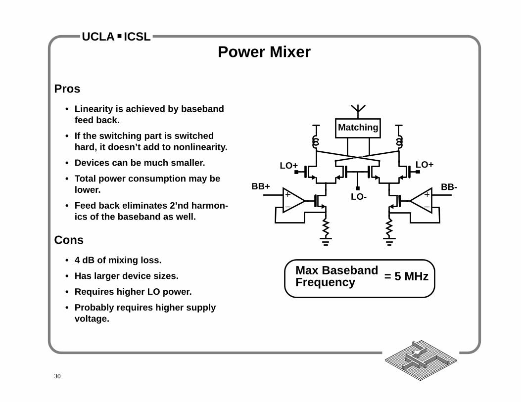
UCLA ■ ICSLCircuit IdeasPower Mixer
Σ PowerAmp
13 dBm3 dBm
• Linearizing MOS by having small ac/DCcurrent ➜
large devices & low efficiency.
• Power-amp has large input capacitor.
• Small inductor for tuning the largecapacitor produces small impedance.
• High current consumption in mixers
Conventional Method
Σ
Alternative Method
13 dBm
• Using high-power mixers to generate13 dBm required output power.
• Using feedback in the baseband ofthe mixer for linearization.
• Smaller devices can be used.
30
UCLA ■ ICSLPower Mixer
Pros
• Linearity is achieved by basebandfeed back.
• If the switching part is switchedhard, it doesn’t add to nonlinearity.
• Devices can be much smaller.
• Total power consumption may belower.
• Feed back eliminates 2’nd harmon-ics of the baseband as well.
Cons
• 4 dB of mixing loss.
• Has larger device sizes.
• Requires higher LO power.
• Probably requires higher supplyvoltage.
LO-
LO+ LO+
Matching
BB+ BB-
Max BasebandFrequency = 5 MHz

31
UCLA ■ ICSLVCO idea
• Two LC oscillators, couple to eachother.
• Phase noise limited by 1/f noise ofthe devices.
• Coupling through MOSs whichconsumes power and generates1/f noise.
• Coupling through RC circuits.
• Coupling through resistors andcapacitors (lower 1/f noise)
• Additional power consumption incore transistors (larger devicesand higher g m, lower noise)
900 MHz project VCO Idea for improvement

32
UCLA ■ ICSLDAC for DDFS
10 bits, 300 MHz
bit 10bit 9bit 1
MOSCapacitors
Linear MIMCapacitors
NMOSSwitches
60 dBSettling
360 MHz Sampling Frequency
Pure digital CMOSprocess
SupplyCurrent ≅ 8 mA

33
UCLA ■ ICSLSecond AGC
• 0 ~ 80 dB gain with 5 stages.
• Output power = 5 dBm.
• 90 dB gain ↔
20 dB NF & 59 dB output linearity.
• 50 dB gain ↔
45 dB output linearity.
• 0 dB gain ↔
34 dB NF & 50 dB output linearity.
• High gain block turns off at low gain
and low gain block turns off at high gain.
• Bias current: 6~12 mA
Bias
VCont
VCont VBias
Vin+ Vin-
Vout+Vout-
1- Large input signals
2- 0 < Gain < 6 dB
3- 1 mA bias current
1- Zero output @ large input
2- 0 < Gain < 16 dB3- Low noise
4- 1.5 mA bias current

34
UCLA ■ ICSL
Impact & Achievements
• Demonstrate the capabilities of CMOS for 2.4 GHz band. Significantcontribution to the definition of a new superior MOS model forindustrial standard.
• Develope a highly linear, wide dynamic range, low noise CMOStransceiver:
Tight specifications for building blocks demand innovativedesign leading to new techniques or significant improvementsin the current techniques for each block.
• Achieve ultimate performance of the quadrature architecture.
• Highly integrated circuit. Minimum off-chip components.Highly reliable (fewer components for the whole system).