Embed Size (px)
Citation preview

Application ReportSNAA079C–May 2004–Revised May 2004
AN-236 An Introduction to the Sampling Theorem.....................................................................................................................................................
ABSTRACT
With rapid advancement in data acquistion technology (i.e. analog-to-digital and digital-to-analogconverters) and the explosive introduction of micro-computers, selected complex linear and nonlinearfunctions currently implemented with analog circuitry are being alternately implemented with sample datasystems.
Contents1 An Introduction to the Sampling Theorem ............................................................................... 32 An Intuitive Development .................................................................................................. 33 The Sampling Theorem .................................................................................................... 54 Some Observations and Definitions ...................................................................................... 85 The Sampling Theorem and Its Hardware ............................................................................... 9
5.1 IMPLICATIONS .................................................................................................... 96 A Final Note ................................................................................................................ 177 Acknowledgements ........................................................................................................ 178 ARTICLE REFERENCES ................................................................................................ 17Appendix A Basic Filter Concepts ............................................................................................ 19
List of Figures
1 When sampling, many signals may be found to have the same set of data points. These are calledaliases of each other........................................................................................................ 4
2 Shown in the shaded area is an ideal, low pass, anti-aliasing filter response. Signals passed through thefilter are bandlimited to frequencies no greater than the cutoff frequency, fc. In accordance with thesampling theorem, to recover the bandlimited signal exactly the sampling rate must be chosen to begreater than 2fc.............................................................................................................. 4
3 Fourier transform of a sampled signal.................................................................................... 7
4 Recovery of a signal f(t) from sampled data information............................................................... 7
5 Spectral folding or aliasing caused by: (a) under sampling (b) exaggerated under sampling. ................... 8
6 Aliased spectral envelope (a) and (b) of a and b respectively. ....................................................... 9
7 Generalized single channel sample data system. ...................................................................... 9
8 Typical filter magnitude and phase versus frequency response..................................................... 11
9 ............................................................................................................................... 12
10 (c) equals the convolution of (a) with (b). .............................................................................. 12
11 Quantization error.......................................................................................................... 14
12 Amplitude uncertainty as a function of (a) a nonvarying aperture and(b) aperture time uncertainty. .......... 14
13 The Fourier transform of the rectangular pulse (a) is shown in (b). ................................................ 15
14 Sampling Pulse (a), its Magnitude (b) and Phase Response (c). ................................................... 15
15 Pulse width and how it effects the sin X/X envelop spectrum (normalized amplitudes).......................... 16
16 (a) Processed signal data points (b) output of D/A converter (c) output of smoothing filter. .................... 17
17 Common Low Pass Filter Response.................................................................................... 19
18 Common High Pass Filter Response ................................................................................... 19
19 Common Band-pass Filter Response................................................................................... 20
All trademarks are the property of their respective owners.
1SNAA079C–May 2004–Revised May 2004 AN-236 An Introduction to the Sampling TheoremSubmit Documentation Feedback
Copyright © 2004, Texas Instruments Incorporated

www.ti.com
20 Common Band-Reject Filter Response................................................................................. 20
2 AN-236 An Introduction to the Sampling Theorem SNAA079C–May 2004–Revised May 2004Submit Documentation Feedback
Copyright © 2004, Texas Instruments Incorporated

www.ti.com An Introduction to the Sampling Theorem
1 An Introduction to the Sampling Theorem
With rapid advancement in data acquistion technology (i.e. analog-to-digital and digital-to-analogconverters) and the explosive introduction of micro-computers, selected complex linear and nonlinearfunctions currently implemented with analog circuitry are being alternately implemented with sample datasystems.
Though more costly than their analog counterpart, these sampled data systems feature programmability.Additionally, many of the algorithms employed are a result of developments made in the area of signalprocessing and are in some cases capable of functions unrealizable by current analog techniques.
With increased usage a proportional demand has evolved to understand the theoretical basis required ininterfacing these sampled data-systems to the analog world.
This article attempts to address the demand by presenting the concepts of aliasing and the samplingtheorem in a manner, hopefully, easily understood by those making their first attempt at signal processing.Additionally discussed are some of the unobvious hardware effects that one might encounter whenapplying the sampled theorem.
With this. . . let us begin.
2 An Intuitive Development
The sampling theorem by C.E. Shannon in 1949 places restrictions on the frequency content of the timefunction signal, f(t), and can be simply stated as follows:
— In order to recover the signal function f(t) exactly, it is necessary to sample f(t) at a rate greaterthan twice its highest frequency component.
Practically speaking for example, to sample an analog signal having a maximum frequency of 2Kcrequires sampling at greater than 4Kc to preserve and recover the waveform exactly.
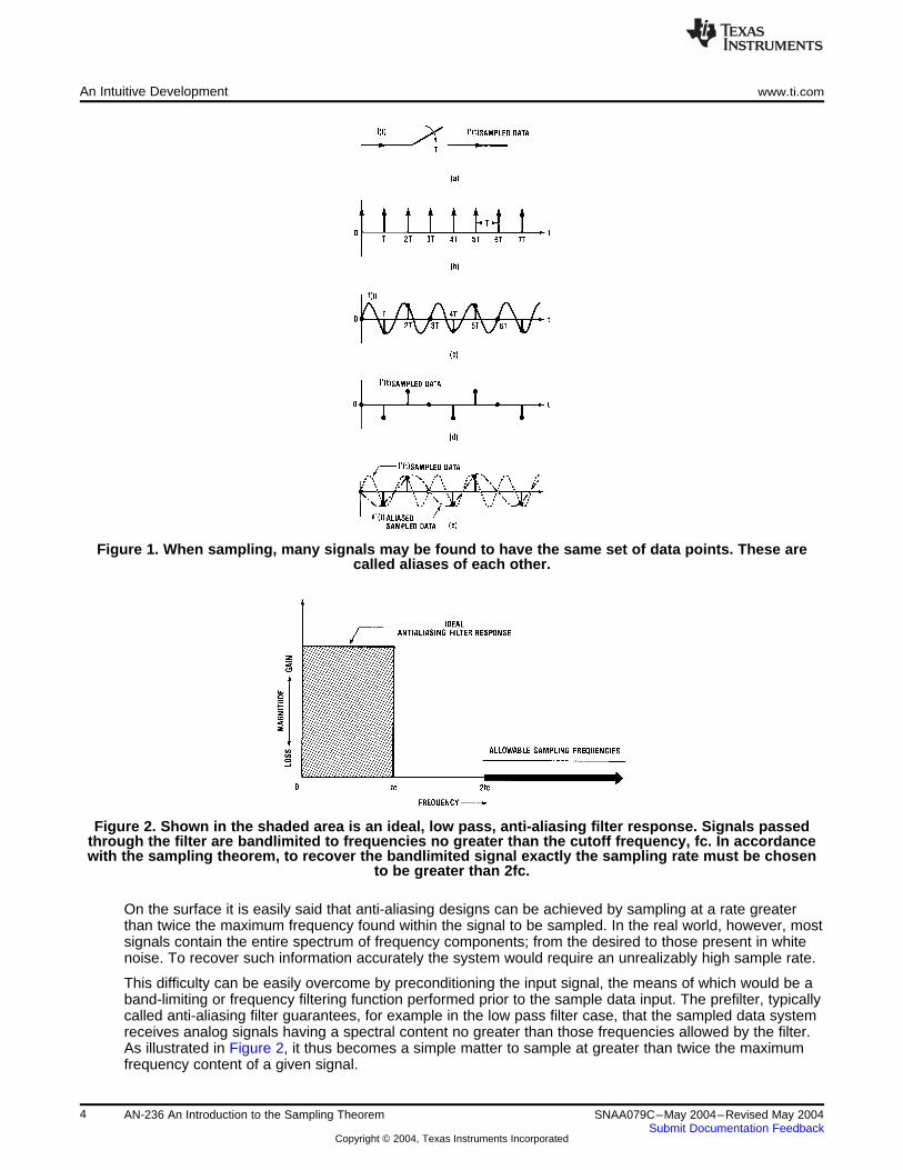
The consequences of sampling a signal at a rate below its highest frequency component results in aphenomenon known as aliasing. This concept results in a frequency mistakenly taking on the identity of anentirely different frequency when recovered. In an attempt to clarify this, envision the ideal sampler ofFigure 1(a), with a sample period of T shown in Figure 1(b), sampling the waveform f(t) as pictured inFigure 1(c). The sampled data points of f'(t) are shown in Figure 1(d) and can be defined as the sampleset of the continuous function f(t). Note in Figure 1(e) that another frequency component, a'(t), can befound that has the same sample set of data points as f'(t) in Figure 1(d). Because of this it is difficult todetermine which frequency a'(t), is truly being observed. This effect is similar to that observed in westernmovies when watching the spoked wheels of a rapidly moving stagecoach rotate backwards at a slowrate. The effect is a result of each individual frame of film resembling a discrete strobed samplingoperation flashing at a rate slightly faster than that of the rotating wheel. Each observed sample point orframe catches the spoked wheel slightly displaced from its previous position giving the effectiveappearance of a wheel rotating backwards. Again, aliasing is evidenced and in this example it becomesdifficult to determine which is the true rotational frequency being observed.
3SNAA079C–May 2004–Revised May 2004 AN-236 An Introduction to the Sampling TheoremSubmit Documentation Feedback
Copyright © 2004, Texas Instruments Incorporated
An Intuitive Development www.ti.com
Figure 1. When sampling, many signals may be found to have the same set of data points. These arecalled aliases of each other.
Figure 2. Shown in the shaded area is an ideal, low pass, anti-aliasing filter response. Signals passedthrough the filter are bandlimited to frequencies no greater than the cutoff frequency, fc. In accordancewith the sampling theorem, to recover the bandlimited signal exactly the sampling rate must be chosen
to be greater than 2fc.
On the surface it is easily said that anti-aliasing designs can be achieved by sampling at a rate greaterthan twice the maximum frequency found within the signal to be sampled. In the real world, however, mostsignals contain the entire spectrum of frequency components; from the desired to those present in whitenoise. To recover such information accurately the system would require an unrealizably high sample rate.
This difficulty can be easily overcome by preconditioning the input signal, the means of which would be aband-limiting or frequency filtering function performed prior to the sample data input. The prefilter, typicallycalled anti-aliasing filter guarantees, for example in the low pass filter case, that the sampled data systemreceives analog signals having a spectral content no greater than those frequencies allowed by the filter.As illustrated in Figure 2, it thus becomes a simple matter to sample at greater than twice the maximumfrequency content of a given signal.
4 AN-236 An Introduction to the Sampling Theorem SNAA079C–May 2004–Revised May 2004Submit Documentation Feedback
Copyright © 2004, Texas Instruments Incorporated

www.ti.com The Sampling Theorem
A parallel analog of band-limiting can be made to the world of perception when considering the spectrumof white light. It can be realized that the study of violet light wavelengths generated from a white lightsource would be vastly simplified if initial band-limiting were performed through the use of a prism or whitelight filter.
3 The Sampling Theorem
To solidify some of the intuitive thoughts presented in the previous section, the sampling theorem will bepresented applying the rigor of mathematics supported by an illustrative proof. This should hopefully leavethe reader with a comfortable understanding of the sampling theorem.
Theorem: — If the Fourier transform F(ω) of a signal function f(t) is zero for all frequencies above |ω| ≥ωc, then f(t) can be uniquely determined from its sampled values
fn = f(nT) (1)
These values are a sequence of equidistant sample points spaced apart. (f)t is thus given by
(2)
Proof: Using the inverse Fourier transform formula:
(3)
the band limited function, f(t), takes the form, Figure 3a,
(4)
(5)
(6)
See Figure 3c and Figure 3e.
Expressing F(ω) as a Fourier series in the interval −ωc ≤ ω ≤ ωc we have
(7)
Where,
(8)
Further manipulating Equation 8
(9)
Cn can be written as
(10)
Substituting Equation 10 into Equation 7 gives the periodic Fourier Transform
(11)
of Figure 3f. Using Poisson's sum formula F(ω) can be stated more clearly as
(12)
5SNAA079C–May 2004–Revised May 2004 AN-236 An Introduction to the Sampling TheoremSubmit Documentation Feedback
Copyright © 2004, Texas Instruments Incorporated

The Sampling Theorem www.ti.com
Interestingly for the interval −ωc ≤ ω ≤ ωc the periodic function Fp(ω) and Figure 3f. equals F(ω) andFigure 3b. respectively. Analogously if Fp(ω) were multiplied by a rectangular pulse defined,
H(ω) = 1 −ωc ≤ ω ≤ ω (13)
andH(ω) = 0 |ω| ≥ ωC (14)
then as pictured in Figure 4b, d, and f,
(15)
Solving for f(t) the inverse Fourier transform Equation 3 is applied to Equation 15
(16)
(17)
(1) (18)
where and fs is the sampling frequency
giving
(19)
Equation 19 is equivalent to Equation 2 as is illustrated in Figure 4e and Figure 3a respectively.
As observed in Figure 3 and Figure 4, each step of the sampling theorem proof was also illustrated with itsFourier transform pair. This was done to present alternate illustrative proofs.
Recalling the convolution theorem, the convolution of F(ω), Figure 3b, with a set of equidistant impulses,Figure 3d, yields the same periodic frequency function Fp(ω), Figure 3f, as did the Fourier transform of fn,Figure 3e, the product of f(t), Figure 3a, and its equidistant sample impulses, Figure 3c.
In the same light the original time function f(t), Figure 4e, could have been recovered from its sampledwaveform by convolving fn, Figure 4a, with h(t), Figure 4c, rather than multiplying Fp(ω), Figure 4b, by therectangular function H(ω), Figure 4d, to get F(ω), Figure 4f, and finally inverse transforming to achieve f(t),Figure 4e, as done in the mathematic proof.
(1) Poisson's sum formula
6 AN-236 An Introduction to the Sampling Theorem SNAA079C–May 2004–Revised May 2004Submit Documentation Feedback
Copyright © 2004, Texas Instruments Incorporated

www.ti.com The Sampling Theorem
(2)
Figure 3. Fourier transform of a sampled signal.
Figure 4. Recovery of a signal f(t) from sampled data information.
(2) The convolution theorem allows one to mathematically convolve in the time domain by simply multiplying in the frequency domain. Thatis, if f(t) has the Fourier transform F(ω), and x(t) has the Fourier transform X(ω), then the convolution f(t)*x(t) has the Fourier transformF(ω)•X(ω).f(t) * x(t) ↔ F(ω) • X(ω)f(t) • x(t) ↔ F(ω) * X(ω)
7SNAA079C–May 2004–Revised May 2004 AN-236 An Introduction to the Sampling TheoremSubmit Documentation Feedback
Copyright © 2004, Texas Instruments Incorporated

Some Observations and Definitions www.ti.com
4 Some Observations and Definitions
If Figure 3f or Figure 4b are re-examined it can be noted that the original spectrum Fp(ω), |ω| ≤ ωc, and itsimages Fp(ω), |ω| ≥ ωc, are non-overlapping. On the other hand Figure 5 illustrates spectral folding,overlapping or aliasing of the spectrum images into the original signal spectrum. This aliasing effect is, infact, a result of undersampling and further causes the information of the original signal to beindistinguishable from its images (i.e. Figure 1e). From Figure 6 one can readily see that the signal is thusconsidered non-recoverable.
The frequency |fc| of Figure 3f and Figure 4b is exactly one half the sampling frequency, fc=fs/2, and isdefined as the Nyquist frequency (after Harry Nyquist of Bell Laboratories). It is also often called thealiasing frequency or folding frequency for the reasons discussed above. From this we can say that inorder to prevent aliasing in a sampled-data system the sampling frequency should be chosen to begreater than twice the highest frequency component fc of the signal being sampled.
By definitionfs ≥ 2fc (20)
Note, however, that no mention has been made to sample at precisely the Nyquist rate since in actualpractice it is impossible to sample at fs = 2fc unless one can guarantee there are absolutely no signalcomponents above fc. This can only be achieved by filtering the signal prior to sampling with a filter havinginfinite rolloff. . . a physical impossibility, see Figure 2.
Figure 5. Spectral folding or aliasing caused by:(a) under sampling
(b) exaggerated under sampling.
8 AN-236 An Introduction to the Sampling Theorem SNAA079C–May 2004–Revised May 2004Submit Documentation Feedback
Copyright © 2004, Texas Instruments Incorporated

www.ti.com The Sampling Theorem and Its Hardware
Figure 6. Aliased spectral envelope (a) and (b) ofFigure 5a and Figure 5b respectively.
Figure 7. Generalized single channel sample data system.
5 The Sampling Theorem and Its Hardware
5.1 IMPLICATIONS
Though there are numerous sophisticated techniques of implementation, it is appropriate to re-emphasizethat the intent of this article is to give the first time user a basic and fundamental approach toward thedesign of a sampled-data system. The method with which to achieve this goal will be to introduce a few ofthe common perils encountered when implementing such a system. We begin by considering thegeneralized block diagram of Figure 7.
As shown in Figure 7, prior to any signal processing manipulation the analog input signal must bepreconditioned to prevent aliasing and thereafter digitized to logic signals usable by the logic functionblock. The antialiasing and digitizing functions are performed by an input filter and analog-to-digitalconverter respectively. Once digitized the signal can then be altered or processed and upon completion,reconstructed back to a continuous analog signal via a digital-to-analog converter followed by a smoothingfilter.
To this point no mention has been made concerning the sample and hold circuit block depicted inFigure 7. In general the analog-to-digital converter can operate as a stand alone unit. In many high speedoperations however, the converter speed is insufficient and thus requires the assistance of a sample andhold circuit. This will be discussed in detail further in the article.
5.1.1 The Antialiasing Input Filter
As indicated earlier in the text, the antialiasing filter should band-limit the input signal's spectrum tofrequencies no greater than the Nyquist frequency. In the real world however, filters are non-ideal andhave typical attenuation or band-limiting and phase characteristics as shown in Figure 8 . It must also berealized that true band-limiting of a specific frequency spectrum is not possible. In the sample data systemband-limiting is achieved by attenuating those frequencies greater than the Nyquist frequency to a levelundetectable or invisible to the system analog-to-digital (A/D) converter. This level would typically be lessthan the rms quantization noise level defined by the specific converter being used.
9SNAA079C–May 2004–Revised May 2004 AN-236 An Introduction to the Sampling TheoremSubmit Documentation Feedback
Copyright © 2004, Texas Instruments Incorporated

The Sampling Theorem and Its Hardware www.ti.com
(3) (4)As an example of how an antialiasing filter would be applied, assume a sample data system havingwithin it an 8-bit A/D converter. Eight bits translates to 2n=28=256 levels of resolution. If a 2.56 voltreference were used each quantization level, q, would represent the equivalent of 2.56 volts/256=10millivolts. Realizing this the antialiasing filter would be designed such that frequencies in the stopbandwere attenuated to less than the rms quantization noise level of and thus appearing invisible to thesystem. More specifically
(21)
It can be seen, for example in the Butterworth filter case (characterized as having a maximally flat pass-band) of Figure 9a that any order of filter may be used to achieve the −59 dB attenuation level, however,the higher the order, the faster the roll off rate and the closer the filter magnitude response will approachthe ideal.
Referring back to Figure 8 it is observed that those frequencies greater than ωa are not recognized by theA/D converter and thus the sampling frequency of the sample data system would be defined as ωs ≥ 2ωa.Additionally, the frequencies present within the filtered input signal would be those less than ωa. Notehowever, that the portion of the signal frequencies least distorted are those between ω=O and ωp andthose within the transition band are distorted to a substantial degree, though it was originally desired tolimit the signal to frequencies less than the cutoff ωp, because of the non-ideal frequency response thetrue Nyquist frequency occurred at ωa. We see then that the sampled-data system could at most beaccurate for those frequencies within the antialiasing filter passband.
From the above example, the design of an antialiasing filter appears to be quite straight forward. Recallhowever, that all waveforms are composed of the sums and differences of various frequency componentsand as a result, if the response of the filter passband were not flat for the desired signal frequencyspectrum, the recovered signal would be an inaccurate summation of all frequency components altered bytheir relative attenuations in the pass-band.
Additionally the antialiasing filter design should not neglect the effects of delay. As illustrated in Figure 8and Figure 9b, delay time corresponds to a specific phase shift at a particular frequency. Similar to the flatpass-band consideration, if the phase shift of the filter is not exactly proportional to the frequency, theoutput of the filter will be a waveform in which the summation of all frequency components has beenaltered by shifts in their relative phase. Figure 9b further indicates that contrary to the roll off rate, thehigher the filter order the more non-ideal the delay becomes (increased delay) and the result is a distortedoutput signal.
A final and complex consideration to understand is the effects of sampling. When a signal is sampled theend effect is the multiplication of the signal by a unit sampling pulse train as recalled from Figure 3a, c ande. The resultant waveform has a spectrum that is the convolution of the signal spectrum and the spectrumof the unit sample pulse train, i.e. Figure 3b, d, and f. If the unit sample pulse has the classical sin X/Xspectrum of a rectangular pulse, see Figure 13, then the convolution of the pulse spectrum with the signalspectrum would produce the non-ideal sampled signal spectrum shown in Figure 10a, b, and c.
It should be realized that because of the band-limiting or filtering and delay response of the Sin X/Xfunction combined with the effects of the non-ideal antialiasing filter (i.e. non-flat pass-band and phaseshift) certain of the sum and difference frequency components may fall within the desired signal spectrumthereby creating aliasing errors, Figure 10c.
When designing antialiasing filters it will be found that the closer the filter response approaches the idealthe more complex the filter becomes. Along with this an increase in delay and pass-band ripple combineto distort and alias the input signal. In the final analysis the design will involve trade offs made betweenfilter complexity, sampling speed and thus system bandwidth.
(3) In order not to disrupt the flow of the discussion a list of filter terms has been presented in Appendix A.(4) For an explanation of quantization refer to section IV. B. of this article.
10 AN-236 An Introduction to the Sampling Theorem SNAA079C–May 2004–Revised May 2004Submit Documentation Feedback
Copyright © 2004, Texas Instruments Incorporated

www.ti.com The Sampling Theorem and Its Hardware
(5)
Figure 8. Typical filter magnitude and phase versus frequency response.
a) Attenuation characteristics of a normalized Butterworth filter as a function of degree n.
(5) This will be explained more clearly in Section IV. of this article.
11SNAA079C–May 2004–Revised May 2004 AN-236 An Introduction to the Sampling TheoremSubmit Documentation Feedback
Copyright © 2004, Texas Instruments Incorporated

The Sampling Theorem and Its Hardware www.ti.com
b) Group delay performances of normalized Butterworth lowpass filters as a function of degree n.
Figure 9.
Figure 10. (c) equals the convolution of (a) with (b).
5.1.2 The Analog-to-Digital Converter
Following the antialiasing filter is the A/D converter which performs the operations of quantizing andcoding the input signal in some finite amount of time. Figure 11 shows the quantization process ofconverting a continuous analog input signal into a set of discrete output levels. A quantization, q, is thusdefined as the smallest step used in the digital
12 AN-236 An Introduction to the Sampling Theorem SNAA079C–May 2004–Revised May 2004Submit Documentation Feedback
Copyright © 2004, Texas Instruments Incorporated

www.ti.com The Sampling Theorem and Its Hardware
representation of fq(n) where f(n) is the sample set of an input signal f(t) and is expressed by a finitenumber of bits giving the sequence fq(n). Digitally speaking q is the value of the least significant code bit.The difference signal ε(n) shown in Figure 11 is called quantization noise or error and can be defined asε(n) = f(n) − fq(n). This error is an irreducible one and is a function of the quantizing process. Its erroramplitude is dependent on the number of quantization levels or quantizer resolution and as shown, themaximum quantization error is |q/2|.
Generally ε(n) is treated as a random error when described in terms of its probability density function, thatis, all values of ε(n) between q/2 and −q/2 are equally probable, then for the average value ε(n)avg=0 andfor the rms value
As a side note it is appropriate at this point to emphasize that all analog signals have some form of noisecorruption. If for example an input signal has a finite signal-to-noise ratio of 40dB it would be superfluousto select an A/D converter with a high number of bits. It may be realized that the use of a large number ofbits does not give the digitized signal a higher signal-to-noise ratio than that of the original analog inputsignal. As a supportive argument one may say that though the quantization steps q are very small withrespect to the peak input signal the lower order bits of the A/D converter merely provide a more accuraterepresentation of the noise inherent in the analog input signal.
Returning to our discussion, we define the conversion time as the time taken by the A/D converter toconvert the analog input signal to its equivalent quantization or digital code. The conversion speedrequired in any particular application depends upon the time variation of the signal to be converted and theamount of resolution or bits, n, required. Though the antialiasing filter helps to control the input signal timerate of change by band-limiting its frequency spectrum, a finite amount of time is still required to make ameasurement or conversion. This time is generally called the aperture time and as illustrated in Figure 12produces amplitude measurement uncertainty errors. The maximum rate of change detectable by an A/Dconverter can simply be stated as
(22)
If for example V full scale = 10.24 volts, T conversion time = 10 ms, and n = 10 or 1024 bits of resolutionthen the maximum rate of change resolvable by the A/D converter would be 1 volt/sec. If the input signalhas a faster rate of change than 1 volt/sec, 1 LSB changes cannot be resolved within the sampling period.
In many instances a sample-and-hold circuit may be used to reduce the amplitude uncertainty error bymeasuring the input signal with a smaller aperture time than the conversion time aperture of the A/Dconverter. In this case the maximum rate of change resolvable by the sample-and-hold would be
(23)
Note also that the actual calculated rate of change may be limited by the slew rate specification fo thesample-and-hold in the track mode. Additionally it is very important to clarify that this does not implyviolating the sampling theorem in lieu of the increased ability to more accurately sample signals having afast time rate of change.
13SNAA079C–May 2004–Revised May 2004 AN-236 An Introduction to the Sampling TheoremSubmit Documentation Feedback
Copyright © 2004, Texas Instruments Incorporated

The Sampling Theorem and Its Hardware www.ti.com
Figure 11. Quantization error.
ΔV: AMPLITUDE UNCERTAINTY ERRORta: APERTURE TIMEΔta: APERTURE TIME UNCERTAINTY
Figure 12. Amplitude uncertainty as a function of (a) a nonvarying aperture and(b) aperture timeuncertainty.
An ideal sample-and-hold effectively takes a sample in zero time and with perfect accuracy holds thevalue of the sample indefinitely. This type of sampler is also known as a zero order hold circuit and itseffect on a sample data system warrants some discussion.
It is appropriate to recall the earlier discussion that the spectrum of a sampled signal is one in which theresultant spectrum is the product obtain by convolving the input signal spectrum with the sin X/X spectrumof the sampling waveform. Figure 13 illustrates the frequency spectrum plotted from the Fourier transform
(24)
of a rectangular pulse. The sin X/X form occurs frequently in modern communication theory and iscommonly called the sampling function.
The magnitude and phase of a typical zero order hold sampler spectrum
(25)
is shown in Figure 14 and Figure 15 illustrates the spectra of various sampler pulse-widths. The purposeof presenting this illustrative information is to give insight at to what effects cause the aliasing described inFigure 10. From Figure 15 it is realized that the main lobe of the sin X/X function varies inverselyproportional with the sampler pulse-width. In other words a wide pulse-width, or in this case the aperturewindow, acts as a low pass filtering function and limits the amount of information resolvable by the sample
14 AN-236 An Introduction to the Sampling Theorem SNAA079C–May 2004–Revised May 2004Submit Documentation Feedback
Copyright © 2004, Texas Instruments Incorporated

www.ti.com The Sampling Theorem and Its Hardware
data system. On the other hand a narrow sampler pulse-width or aperture window has a broader mainlobe or band-width and thus when convolved with the analog input signal produces the least amount ofdistortion. Understandably then the effect of the sampler's spectral phase and main lobe width must beconsidered when developing a sampling system so that no unexpected aliasing occurs from itsconvolution with the input signal spectrum.
Figure 13. The Fourier transform of the rectangularpulse (a) is shown in (b).
Figure 14. Sampling Pulse (a), its Magnitude (b) and Phase Response (c).
15SNAA079C–May 2004–Revised May 2004 AN-236 An Introduction to the Sampling TheoremSubmit Documentation Feedback
Copyright © 2004, Texas Instruments Incorporated

The Sampling Theorem and Its Hardware www.ti.com
Figure 15. Pulse width and how it effects the sin X/Xenvelop spectrum (normalized amplitudes).
5.1.3 The Digital-to-Analog Converter and Smoothing Filter
After a signal has been digitally conditioned by the signal processing unit of Figure 7, a D/A converter isused to convert the sampled binary information back in to an analog signal. The conversion is called azero order hold type where each output sample level is a function of its binary weight value and is helduntil the next sample arrives, see Figure 16. As a result of the D/A converter step function response it isapparent that a large amount of undesirable high frequency energy is present. To eliminate this the D/Aconverter is usually followed by a smoothing filter, having a cutoff frequency no greater than half thesampling frequency. As its name suggests the filter output produces a smoothed version of the D/Aconverter output which in fact is a convolved function. More simply said, the spectrum of the resultingsignal is the product of a step function sin X/X spectrum and the band-limited analog filter spectrum.Analogous to the input sampling problem, the smoothed output may have aliasing effects resulting fromthe phase and attenuation relations of the signal recovery system (defined as the D/A converter andsmoothing filter combination).
As a final note, the attenuation due to the D/A converter sin X/X spectrum shape may in some cases becompensated for in the signal processing unit by pre-processing using a digital filter with an inverseresponse X/sin X prior to D/A conversion. This allows an overall flat magnitude signal response to besmoothed by the final filter.
16 AN-236 An Introduction to the Sampling Theorem SNAA079C–May 2004–Revised May 2004Submit Documentation Feedback
Copyright © 2004, Texas Instruments Incorporated

www.ti.com A Final Note
Figure 16. (a) Processed signal data points (b) output of D/A converter (c) output of smoothing filter.
6 A Final Note
This article began by presenting an intuitive development of the sampling theorem supported by amathematical and illustrative proof. Following the theoretical development were a few of the unobviousand troublesome results that develop when trying to put the sampling theorem into practice. The purposeof presenting these thought provoking perils was to perhaps give the beginning designer some insight orguidelines for consideration when developing a sample data system's interface.
7 Acknowledgements
The author wishes to thank James Moyer and Barry Siegel for their encouragement and the time theyallocated for the writing of this article.
8 ARTICLE REFERENCES• S.D. Stearns, Digital Signal Analysis, Hayden, 1975
• S.A. Tretter, Introduction to Discrete-Time Signal Processing, Wiley, 1976
• W.D. Stanley, Digital Signal Processing, Reston, 1975
• A. Papoulis, The Fourier Integral and its Applications, Mc-Graw-Hill, 1962
• E.A. Robinson, M. T. Silvia, Digital Signal Processing and Time Series Analysis, Holden-Day, 1978
• C.E. Shannon, “Communication in the Presence of Noise,” Proceedings IRE, Vol. 37, pp. 10–21, Jan.1949
• M. Schwartz, L. Shaw, Signal Processing: Discrete Spectral Analysis, Detection and Estimation,McGraw-Hill, 1975
• L.R. Rabiner, B. Gold, Theory and Application of Digital Signal Processing, Prentice-Hall, 1975
• W.H. Hayt, J.E. Kemmerly, Engineering Circuit Analysis, McGraw-Hill, 3rd edition, 1978
• E.O. Brigham, The Fast Fourier Transform, Prentice-Hall, 1974
• J. Sherwin, Specifying A/D and D/A converters, National Semiconductor Corp., Application Note AN-156
• Analog-Digital Conversion Notes, Analog Devices Inc., 1974
17SNAA079C–May 2004–Revised May 2004 AN-236 An Introduction to the Sampling TheoremSubmit Documentation Feedback
Copyright © 2004, Texas Instruments Incorporated

ARTICLE REFERENCES www.ti.com
• A.I. Zverev, Handbook of Filter Synthesis, Wiley, 1967
18 AN-236 An Introduction to the Sampling Theorem SNAA079C–May 2004–Revised May 2004Submit Documentation Feedback
Copyright © 2004, Texas Instruments Incorporated

www.ti.com
Appendix A Basic Filter Concepts
A filter is a network used for separating signal waves on the basis of their frequency and is usuallycomposed of passive, reactive and active elements such as resistors, capacitors, inductors, andamplifiers, or combinations thereof.
There are basically five types of filters used to pass or reject such signals and they are defined as follows:
1. A low-pass filter passes a band of frequencies called the passband, ranging from zero frequency or DCto a certain cutoff frequency, ωc, and in addition has a maximum attenuation or ripple level of AMAX
within the passband. See Figure 17.
• Frequencies beyond the ωc may have an attenuation greater than AMAX but beyond a specificfrequency ωs defined as the stopband frequency, a minimum attenuation of AMIN must prevail. Theband of frequencies higher than ωs and maintaining attenuation greater than or equal to AMIN iscalled the stopband. The transition region or transition band is that band of frequencies betweenωc and ωs.
(6)
Figure 17. Common Low Pass Filter Response
A high-pass filter allows frequencies above the passband frequency, ωc, to pass and rejects frequenciesbelow this point. AMAX must be maintained in the passband and frequencies equal to and below thestopband frequency, ωs, must have a minimum attenuation of AMIN. See Figure 18.
Figure 18. Common High Pass Filter Response
A bandpass filter performs the function of passing a specific band of frequencies while rejecting thosefrequencies above and below ωc2 and lower, ωc1 cutoff frequency limits. See Figure 19.
As in the previous two cases the passband is required to sustain an attenuation of AMAX, and the stopbandof frequencies above and below ωs2 and ωs2 respectively, must have a minimum attenuation of AMIN.
(6) Recall that the radian frequency ω=2πf.
19SNAA079C–May 2004–Revised May 2004 AN-236 An Introduction to the Sampling TheoremSubmit Documentation Feedback
Copyright © 2004, Texas Instruments Incorporated

Appendix A www.ti.com
Figure 19. Common Band-pass Filter Response
A band-reject filter or notch filter allows all but a specific band of frequencies to pass. As shown inFigure 4, those frequencies between ωs1 and ωs2 are filtered out and those frequencies above and belowωc2 and ωc1 respectively are passed. The attenuation requirements of the stopband AMIN and passbandAMAX must still hold.
Figure 20. Common Band-Reject Filter Response
An all-pass or phase shift filter allows all frequencies to pass without any appreciable attenuation. It furtherintroduces a predictable phase shift to all frequencies passed, though not restricting the entire range offrequencies to a specific phase shift (i.e., a phase shift may be imposed upon a selected band offrequencies and appear invisible to all others).
20 AN-236 An Introduction to the Sampling Theorem SNAA079C–May 2004–Revised May 2004Submit Documentation Feedback
Copyright © 2004, Texas Instruments Incorporated

IMPORTANT NOTICE
Texas Instruments Incorporated and its subsidiaries (TI) reserve the right to make corrections, enhancements, improvements and otherchanges to its semiconductor products and services per JESD46, latest issue, and to discontinue any product or service per JESD48, latestissue. Buyers should obtain the latest relevant information before placing orders and should verify that such information is current andcomplete. All semiconductor products (also referred to herein as “components”) are sold subject to TI’s terms and conditions of salesupplied at the time of order acknowledgment.
TI warrants performance of its components to the specifications applicable at the time of sale, in accordance with the warranty in TI’s termsand conditions of sale of semiconductor products. Testing and other quality control techniques are used to the extent TI deems necessaryto support this warranty. Except where mandated by applicable law, testing of all parameters of each component is not necessarilyperformed.
TI assumes no liability for applications assistance or the design of Buyers’ products. Buyers are responsible for their products andapplications using TI components. To minimize the risks associated with Buyers’ products and applications, Buyers should provideadequate design and operating safeguards.
TI does not warrant or represent that any license, either express or implied, is granted under any patent right, copyright, mask work right, orother intellectual property right relating to any combination, machine, or process in which TI components or services are used. Informationpublished by TI regarding third-party products or services does not constitute a license to use such products or services or a warranty orendorsement thereof. Use of such information may require a license from a third party under the patents or other intellectual property of thethird party, or a license from TI under the patents or other intellectual property of TI.
Reproduction of significant portions of TI information in TI data books or data sheets is permissible only if reproduction is without alterationand is accompanied by all associated warranties, conditions, limitations, and notices. TI is not responsible or liable for such altereddocumentation. Information of third parties may be subject to additional restrictions.
Resale of TI components or services with statements different from or beyond the parameters stated by TI for that component or servicevoids all express and any implied warranties for the associated TI component or service and is an unfair and deceptive business practice.TI is not responsible or liable for any such statements.
Buyer acknowledges and agrees that it is solely responsible for compliance with all legal, regulatory and safety-related requirementsconcerning its products, and any use of TI components in its applications, notwithstanding any applications-related information or supportthat may be provided by TI. Buyer represents and agrees that it has all the necessary expertise to create and implement safeguards whichanticipate dangerous consequences of failures, monitor failures and their consequences, lessen the likelihood of failures that might causeharm and take appropriate remedial actions. Buyer will fully indemnify TI and its representatives against any damages arising out of the useof any TI components in safety-critical applications.
In some cases, TI components may be promoted specifically to facilitate safety-related applications. With such components, TI’s goal is tohelp enable customers to design and create their own end-product solutions that meet applicable functional safety standards andrequirements. Nonetheless, such components are subject to these terms.
No TI components are authorized for use in FDA Class III (or similar life-critical medical equipment) unless authorized officers of the partieshave executed a special agreement specifically governing such use.
Only those TI components which TI has specifically designated as military grade or “enhanced plastic” are designed and intended for use inmilitary/aerospace applications or environments. Buyer acknowledges and agrees that any military or aerospace use of TI componentswhich have not been so designated is solely at the Buyer's risk, and that Buyer is solely responsible for compliance with all legal andregulatory requirements in connection with such use.
TI has specifically designated certain components as meeting ISO/TS16949 requirements, mainly for automotive use. In any case of use ofnon-designated products, TI will not be responsible for any failure to meet ISO/TS16949.
Products Applications
Audio www.ti.com/audio Automotive and Transportation www.ti.com/automotive
Amplifiers amplifier.ti.com Communications and Telecom www.ti.com/communications
Data Converters dataconverter.ti.com Computers and Peripherals www.ti.com/computers
DLP® Products www.dlp.com Consumer Electronics www.ti.com/consumer-apps
DSP dsp.ti.com Energy and Lighting www.ti.com/energy
Clocks and Timers www.ti.com/clocks Industrial www.ti.com/industrial
Interface interface.ti.com Medical www.ti.com/medical
Logic logic.ti.com Security www.ti.com/security
Power Mgmt power.ti.com Space, Avionics and Defense www.ti.com/space-avionics-defense
Microcontrollers microcontroller.ti.com Video and Imaging www.ti.com/video
RFID www.ti-rfid.com
OMAP Applications Processors www.ti.com/omap TI E2E Community e2e.ti.com
Wireless Connectivity www.ti.com/wirelessconnectivity
Mailing Address: Texas Instruments, Post Office Box 655303, Dallas, Texas 75265Copyright © 2012, Texas Instruments Incorporated