Embed Size (px)
Citation preview
AN-0974APPLICATION NOTE
One Technology Way • P.O. Box 9106 • Norwood, MA 02062-9106, U.S.A. • Tel: 781.329.4700 • Fax: 781.461.3113 • www.analog.com
Multicarrier TD-SCMA Feasibility
by Brad Brannon, Bill Schofield, and Yang Ming
Rev. 0 | Page 1 of 28
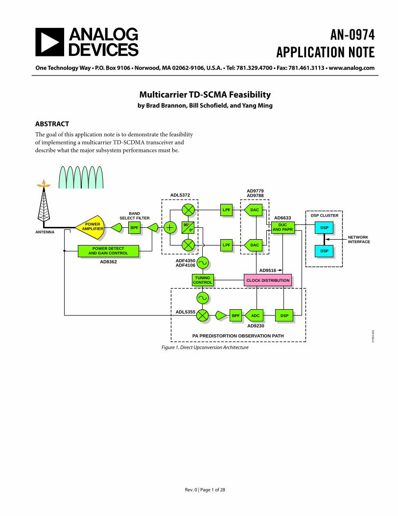
ABSTRACT The goal of this application note is to demonstrate the feasibility of implementing a multicarrier TD-SCDMA transceiver and describe what the major subsystem performances must be.
POWERAMPLIFIER
POWER DETECTAND GAIN CONTROL
ANTENNABPF
BANDSELECT FILTER
90°0°
TUNINGCONTROL
BPF ADC DSP
CLOCK DISTRIBUTION
LPF DAC
LPF DAC
DUCAND PAPR DSP
DSP
DSP CLUSTER
NETWORKINTERFACE
AD6633
AD9516
AD9230
ADL5355
ADF4350ADF4106
AD8362
ADL5372AD9779AD9788
PA PREDISTORTION OBSERVATION PATH
0766
3-00
1
Figure 1. Direct Upconversion Architecture

AN-0974 Application Note
Rev. 0 | Page 2 of 28
TABLE OF CONTENTS Abstract .............................................................................................. 1
Transmit Discussion ......................................................................... 3
General Architecture .................................................................... 3
Carrier Configurations ................................................................ 3
Frequency Error ............................................................................ 3
Physical Layer Structure .............................................................. 4
Power Control ............................................................................... 5
Code Domain Formation ............................................................ 6
Transmit Modulation ................................................................... 6
Transmit Diversity ........................................................................ 7
Peak-to-Average Ratio (Crest Factor) ........................................ 9
Peak-to-Average Power Reduction ............................................ 9
Power Amplifier Linearization ................................................. 11
ACLR ............................................................................................ 14
Signal Chain Analysis ................................................................ 15
Receive Discussion ......................................................................... 21
General Architecture ................................................................. 21
Receiver Requirements .............................................................. 24
Receiver Operating Conditions ................................................ 24
Assumptions ................................................................................ 24
ADC SFDR Requirements ........................................................ 25
Comments on Gain, Fixed or Variable .................................... 26
Validation .................................................................................... 26
Margin for a Six-Carrier Receiver ............................................ 27

Application Note AN-0974
Rev. 0 | Page 3 of 28
TRANSMIT DISCUSSION GENERAL ARCHITECTURE There are several options for the architecture of the transmit signal path. The factors that impact transmit signal elements are introduced, followed by a discussion of the different archi-tectures. Figure 1 shows a direct conversion architecture for an initial point of reference only. Section 6 of 3GPP TS 25.105 describes the transmit signal requirements used throughout this discussion.
CARRIER CONFIGURATIONS TD-SCDMA is a time division system that uses an unpaired bandwidth structure; the same bandwidth allocation is used for both downlink and uplink in a time synchronized manner, allowing dynamic allocation of time slots for either transmit or receive. This allows for a very efficient use of spectrum with asymmetric traffic loads; a high downlink load would more efficiently use spectrum if it were able to occupy lightly loaded uplink spectrum, rather than congesting the available downlink spectrum. The standard allows for three chip rates: 1.28 Mcps, 3.84 Mcps and 7.68 Mcps. The 1.28 Mcps rate is often referred to as TD-SCDMA low chip rate (LCR) with seven main time
slots in one frame. The 3.84 Mcps rate is often referred to as TD-SCDMA high chip rate (HCR) with 15 time slots in one frame. The general channel raster is 200 kHz, with some modes of the 3.84 Mcps and 7.68 Mcps chip rates requiring a 100 kHz channel raster; a general implementation able to handle all chip rates should operate with a 100 kHz channel raster. The channel spacing for each of the chip rates is 1.6 MHz, 5 MHz, and 10 MHz, respectively (see Figure 2).
FREQUENCY ERROR Each base station is required to center carriers at their assigned frequency allocation; the placement of the carriers is subject to a ±0.05 ppm frequency error for wide area networks. With such a frequency placement requirement, base stations typically derive all timing from the same reference clock and, because the same frequency allocation is used for both receive and transmit, the same reference clock source needs to be used for both receive and transmit. Consequently, converter sample rates that are a mul-tiple of 1.28 Mcps are common, such as 30.72 MSPS, 61.44 MSPS, 76.8 MSPS, and 122.88 MSPS, representing multiplication factors of 24, 48, 60, and 96.
1.16MHz1.16MHz
–5MHz +5MHz0
7.68MHz580kHz580kHz
–2.5MHz +2.5MHz0
3.84MHz160kHz160kHz
–800kHz +800kHz0
1.28MHz
0766
3-00
2
Figure 2. TD-SCDMA Carrier Configurations
AN-0974 Application Note
Rev. 0 | Page 4 of 28
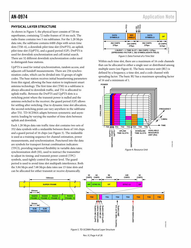
PHYSICAL LAYER STRUCTURE As shown in Figure 5, the physical layer consists of 720 ms superframes, containing 72 radio frames of 10 ms each. The radio frame contains two 5 ms subframes. For the 1.28 Mcps data rate, the subframe contains 6400 chips with seven time slots (TS0–6), a downlink pilot time slot (DwPTS), an uplink pilot time slot (UpPTS), and a guard period (GP). DwPTS is used for downlink synchronization and cell initial search. There are 32 different downlink synchronization codes used to distinguish base stations.
UpPTS is used for initial synchronization, random access, and adjacent cell handoff measurements. There are 256 synchro-nization codes, which can be divided into 32 groups of eight codes. The base station receives initial beamforming parameters from this signal, allowing the base station to implement smart antenna technology. The first time slot (TS0) in a subframe is always allocated to downlink traffic, and TS1 is allocated to uplink traffic. Between the DwPTS and UpPTS slots is a switching point where the transmit power is nulled and the antenna switched to the receiver; the guard period (GP) allows for settling after switching. Due to dynamic time slot allocation, the second switching point can vary anywhere in the subframe after TS1. TD-SCDMA adapts between symmetric and asym-metric loading by varying the number of time slots between uplink and downlink.
Each 1.28 Mcps data rate traffic time slot contains two sets of 352 data symbols with a midamble between them of 144 chips and a guard period of 16 chips (see Figure 3). The midamble is used as a training sequence for channel estimation, power measurements, and synchronization. Punctured into the data are symbols for transport format combination indicators (TFCI), providing improved flexibility in variable data rates; synchronization shift (SS), used to instruct the transmitter to adjust its timing; and transmit power control (TPC) symbols, used tightly control the power level. The guard period is used to avoid time slot multipath interference. Both the 3.84 Mcps and 7.68 Mcps data rates use 15 time slots and can be allocated for either transmit or receive dynamically.
352 CHIPS275µs
144 CHIPS275µs
352 CHIPS275µs
16 CHIPS12.5µs
1 BURST = 1 TIME SLOT = 864 CHIPS = 675µs(SPREADING FACTOR 1, 352 SYMBOLS/DATA FIELD)
TFC
I
SS TPC
TFC
I
0766
3-00
4
GPDATASYMBOLS
DATASYMBOLS
MIDAMBLE
Figure 3. Data Format of a Time Slot
Within each time slot, there are a maximum of 16 code channels that can be allocated to either a single user or distributed among multiple users (see Figure 4). The basic resource unit (RU) is defined by a frequency, a time slot, and a code channel with spreading factor. The basic RU has a maximum spreading factor of 16 and a minimum of 1.
TS1TS0 TS2 TS3 TS4 TS5 TS6
Dw
PTS
SWIT
CH
ING
PO
INT
UpP
TS
SWIT
CH
ING
PO
INTUPLINKTIME SLOTS
DOWNLINKTIME SLOTS
AVAILABLERESOURCEUNIT (RU)
CD
MA
CO
DE
TIME
1.6MHz
FREQUENCY
0766
3-00
5
POWER
Figure 4. Resource Unit
DP SYNC-DL GP SYNC-UL GP
TS0 TS1 TS2 TS3 TS4 TS5 TS6
Dw
PTS
(96
CH
IPS)
SWIT
CH
ING
PO
INT
GP
(96
CH
IPS)
UpP
TS (1
60 C
HIP
S)
TRA
FFIC
TIM
E SL
OT
0-6
(864
CH
IPS)
SWIT
CH
ING
PO
INT
64CHIPS
32CHIPS720msec
96CHIPS
128CHIPS
32CHIPS
SUPER FRAME
10msec
5msec
RADIOFRAME 1
RADIOFRAME 2
SUBFRAME 1
SUBFRAME 2
RADIOFRAME 3
RADIOFRAME 72
0766
3-00
3
Figure 5. TD-SCDMA Physical Layer Structure

Application Note AN-0974
Rev. 0 | Page 5 of 28
POWER CONTROL Power control enables users, in varying channel and loading conditions, to transmit just enough power to meet their quality of service requirements. This strategy increases overall system capacity because the dominant resource allocated among users in CDMA systems is neither time nor frequency slots, but transmit power. Additionally, power control prolongs the battery life of mobile terminals. From the base station’s perspective, there are three types of power control.
Closed-loop power control is operated at 200 Hz for LCR systems and 100 Hz for HCR systems; its main purpose is to ensure the base station transmits just enough power to achieve the desired signal-to-noise ratio (SNR) for the target code channel. The mobile terminal feeds back information about the SNR to the base station in the receive link, requesting it to adjust the power level; the base station instructs the mobile terminal to adjust its power until the desired SNR is just satisfied, hence closing the loop. Closed-loop power control aims at reducing the effects of fast fading. The downlink’s transmit power control bits (TPC) are punctured into the channel’s data stream; the punctured power control bits do not affect the error rate appreciably.
Outer loop power control is used to set the closed-loop power control’s bit error rate thresholds based on quality of service (QoS) requirements for the mobile terminal’s code channel. It is monitored by looking at the frame error rates received from the mobile terminal and aims at reducing fading fluctuations.
Open-loop power control is used to combat slow fading effects; the base station adjusts its power to be inversely proportional to the received signal power. It also acts as a safety fuse when the closed-loop power control fails. When the forward link is lost, the closed-loop reverse link power control can freewheel, and the mobile terminal can interfere with the adjacent cell. The open loop reduces the terminal power as it gets closer to any adjacent cell and limits the possible impact.
The maximum RF output power is defined as the mean power level per carrier measured at the antenna. For a wide area base station, this should be greater than 38 dBm with an integration
bandwidth of 1.28 MHz. The specification allows for power control to be applied to each carrier at the antenna output and on a code channel basis for user quality of service control. The per carrier power control needs to be at least 30 dB. For a system using a single carrier per DAC, the dynamic power control is best placed in a VGA to optimize the dynamic range requirements of the DAC. For a multicarrier system in which there is a common power control setting for all carriers, this should be adjusted in the VGA. It is possible that all but one carrier of a multicarrier system can be 30 dB below the single carrier (see Figure 6); if the spectral performance for a single carrier and for multiple carriers can each be achieved at maxi-mum dynamic power, this scenario would not stress the DAC’s dynamic range requirements any further.
–30dBMINIMUM
0766
3-00
6
Figure 6. TD-SCDMA Carrier Power Control
For code domain power control, the downlink is requested to adjust power with 10 consecutive 1 dB TPC symbols and the transmitter code domain power needs to be between 8 dB and 12 dB. Each code channel’s power needs to have at least a 30 dB range.
When switching between transmit and receive, the power must be controlled to not interfere with the receiver. The guard periods (GP) allow for switching transients. The off power of approximately −144 dBm/Hz would only allow 30 dB of gain from the baseband to the antenna from the thermal noise limit. Because this would be insufficient gain to get to the average on power from the thermal noise limit, the transmit power amplifier the transmit power amplifier need to be either isolated from the antenna or switched during transmit off power periods (see Figure 7).
AVERAGE ON POWER
–42dBm/1.28MHz
–82dBm/1.28MHz(–143dBm/Hz)
8 C
HIP
S
8 C
HIP
S
85 C
HIP
S
DL TIME SLOTS
8 C
HIP
S
3 CHIPS
AVERAGE ON POWER
–33dBm/3.84MHz
–79dBm/3.84MHz(–144.8dBm/Hz)
27 C
HIP
S
31 C
HIP
S
BURSTWITHOUT GP
84 CHIPS
0766
3-00
7
Figure 7. TD-SCDMA Switching

AN-0974 Application Note
Rev. 0 | Page 6 of 28
CODE DOMAIN FORMATION Each users traffic channel is CRC error corrected, convolution encoded, and rate matched before being bit scrambled and mapped to a specific resource unit (RU). The resulting traffic layer data symbols are transferred to the physical layer, where the transmit power control (TPC), transport format combination indicator (TFCI), and synchronization shift symbols are punc-tured into the traffic layer data symbols. The data packet is then mapped to QPSK symbols and spread by channelization codes (orthogonal variable spreading factor, OVSF). The chip rate data is then further spread by a 16-chip complex scrambling code, which for the base station transmitter is either scrambling code 1 or 16. The midamble is then inserted between data packets before being split from polar to complex data streams, which are pulse shaped with a root-raised-cosine filter before being finally upconverted to the desired carrier frequency (see Figure 8).
TRANSMIT MODULATION The TD-SCDMA specification requires two measures of modulation accuracy. The first is peak code domain error, a measure of how well the code channels have been spread and retain their orthogonality. The peak code domain error can be consider code domain noise; if there is too much code domain noise, the receiver’s ability to decorrelate the signal channels correctly is reduced. The code domain noise needs to be main-tained at a minimum level to ensure quality of service to each user. For both 1.28 Mcps and 3.84 Mcps with a spreading factor of 16, the requirement for PCDE is −28 dB.
The second measure of modulation accuracy is error vector magnitude (EVM). By examining the constellation and taking the displacement of each measured dot from the reference position as an error vector (see Figure 9), modulation accuracy can be assessed. The reference position is determined from a reference signal that is synthesized by demodulating the received signal to symbols and then remodulating these symbols perfectly to form the reference constellation. The rms of the error vectors is expressed as a percentage of the overall signal magnitude, called the error vector magnitude (see Figure 9).
0766
3-00
8
USER 0TRAFFIC
CRC ANDTAIL BITS
CONV.ENCODER
RATEMATCHING
QPSKMAPPING
INTERLEAVE SEGMENT
USER 1TRAFFIC
USER NTRAFFIC
TRA
NSP
OR
TC
HA
NN
EL
MU
XBIT
SCRAMBLINGRU
MAPPING
PULSESHAPE
OVSFSPREADING
PULSESHAPE
sin
cos
RE
IMMUX SPLIT
COMPLEXSCRAMBLING
MIDAMBLE
MUXTPC
TFCI
SS
Figure 8. Code Domain Formation
MEASU
RED S
IGNAL
PHASE ERROR(I/Q ERROR
PHASE)
IDEAL SIGNAL
REFERENCE
MAGNITUDE
ERRO
R
(I/Q E
RROR
MAGNITUD
E)
ERROR VECTOR
I
Q
0766
3-00
9
Figure 9. EVM and Constellation of TD-SCDMA Signal

Application Note AN-0974
Rev. 0 | Page 7 of 28
EVM can be calculated as either uncoded or coded EVM. For uncoded EVM, the reference signal is computed from the received bits; therefore, it does not detect coding errors. However, it is sensitive to any impairments that occur in the baseband filters, I/Q modulator, and IF and RF sections of the transmitter. Coded EVM is computed by descrambling and despreading the measured signal to get a reference. The TD-SCDMA specification uses coded EVM and requires 12.5% EVM.
EVM and PCDE are related by the following equation. EVM can be defined as a function of peak-to-average ratio (PAR) and adjacent channel leakage ratio (ACLR).
100101 20(dB)
××=ACLR
PAREVM
⎟⎟⎠
⎞⎜⎜⎝
⎛=
SFEVMPCDE
2
10log10
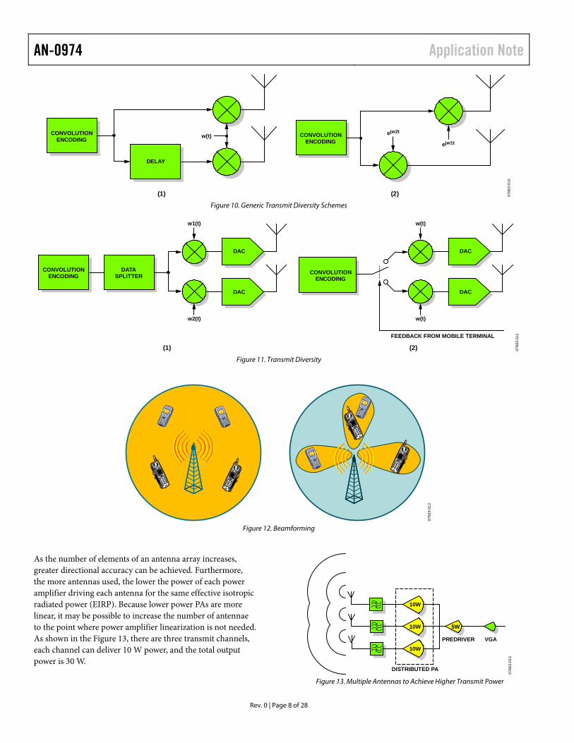
TRANSMIT DIVERSITY Diversity techniques are usually employed to counter the effects of channel fading. The base station’s signal is transmitted through multiple antennae that are spaced far enough apart that the signals emanating from each antenna can be assumed to undergo inde-pendent fading paths. At the mobile terminal, if one of the paths undergo a deep fade, it is unlikely that an auxiliary path is in deep fade and the mobile terminal can recover the signal. Antenna spacing and the velocity of the mobile terminal affects the degree of correlation between the signals at the mobile terminal. Large antenna spacing, on the order of several carrier wavelengths, leads to uncorrelated fading, which leads to maximum perfor-mance gain at the mobile terminal when the velocity of the mobile terminal is slow (pedestrian environment); this channel is characterized as having a flat fading profile. Beamforming methods utilize antenna spacing less than the carrier wavelength, typically half the wavelength and are most suitable for fast moving mobile terminals (vehicular environment); this channel is characterized as having a frequency selective profile.
There are two generic approaches to transmit diversity (see Figure 10). Temporal (delay) diversity, Figure 10(1), transmits a bit stream on one antenna and the same bit stream delayed by one or more sample instants on another antenna. The effect of delay diversity on a slowly fading channel is to allow the mobile terminal to coherently combine the two fading channels, yielding a stronger received signal. This approach suffers from low throughput due to multiple transmissions of the same symbol
over time. Frequency diversity, Figure 10(2), employs transmis-sion of multiple symbol replicas over multiple carriers, each separated in frequency by a sufficiently large amount to ensure independent fading. The effect of frequency diversity for a slow fading channel is similar to temporal diversity in that the mobile terminal coherently combines the two fading channels to aid demodulation. Frequency diversity has the added cost and complexity at both the transmitter and receiver to detect two frequency allocations, and is difficult to implement in a band-limited spectrum.
Transmit diversity in TD-SCDMA systems are generally based on temporal diversity techniques, exploiting the fact that spreading codes are by their nature orthogonal and can be slipped by one symbol period to get the delay element in the temporal diversity scheme.
There are two classes of transmit diversity used in TD-SCDMA. In open-loop transmit diversity (for example, orthogonal transmit diversity, Figure 11(1)), the encoded data stream is split into two different streams for simultaneous transmission over different transmit antennae. Different spreading codes are used for both streams to maintain the orthogonality. To maintain the effective number of spreading codes per user as in the single antenna configuration, the spreading length is doubled. The second class of transmit diversity is closed-loop transmit diversity (for example, selection transmit diversity, Figure 11(2). The power received by the mobile terminal may not yield the highest signal-to-noise ratio under fading conditions. Ideally, one would want the trans-mitter to choose the antenna that yields the highest received signal-to-noise ratio. However, this is not possible because the transmitter does not know the state of the channel between the base station and the mobile terminal; therefore, a feedback channel is used from the mobile terminal to the base station, indicating which of the two antennae has a higher received signal-to-noise ratio.
Of the two classes of transmit diversity available to TD-SCDMA, open-loop schemes appear to offer greater advantages to fast moving mobile terminals, whereas the closed-loop schemes are best at overcoming flat fading channels, more common to slow moving mobile terminals. One of the greatest advantages of using beamforming techniques is to reduce intracell interfe-rence by directing transmit power only in the direction that is needed for the specific mobile, and not in the direction of other mobiles. This is very effective for controlling transmit power and for increasing mobile receive sensitivity (see Figure 12).
AN-0974 Application Note
Rev. 0 | Page 8 of 28
0766
3-01
0
(1) (2)
CONVOLUTIONENCODING
CONVOLUTIONENCODING
DELAY
w(t) ejw2t
ejw1t
Figure 10. Generic Transmit Diversity Schemes
0766
3-01
1
(2)
CONVOLUTIONENCODING
w(t)
w(t)
DAC
DAC
FEEDBACK FROM MOBILE TERMINAL
(1)
CONVOLUTIONENCODING
w1(t)
w2(t)
DAC
DAC
DATASPLITTER
Figure 11. Transmit Diversity
0766
3-01
2
Figure 12. Beamforming
As the number of elements of an antenna array increases, greater directional accuracy can be achieved. Furthermore, the more antennas used, the lower the power of each power amplifier driving each antenna for the same effective isotropic radiated power (EIRP). Because lower power PAs are more linear, it may be possible to increase the number of antennae to the point where power amplifier linearization is not needed. As shown in the Figure 13, there are three transmit channels, each channel can deliver 10 W power, and the total output power is 30 W.
10W
10W 5W
10WPREDRIVER VGA
DISTRIBUTED PA
0766
3-01
3
Figure 13. Multiple Antennas to Achieve Higher Transmit Power

Application Note AN-0974
Rev. 0 | Page 9 of 28
The implication for the converters is that the number of DACs should match the number of antennae being used, preferably with a matched transfer function. Thus, single chip dual DACs, such as the AD9767, AD9777, and AD9779, are ideal for two antenna systems.
PEAK-TO-AVERAGE RATIO (CREST FACTOR) The power amplifier, which drives the antenna, has opposing performance metrics when considering efficiency and linearity. The amplifier is most efficient when driven into saturation, but also has its worst linearity in saturation. Conversely, an amplifier driven for linearity is highly inefficient. Typically, a compromise is found between linearity and efficiency; the average operating point is set such that the signal crests are just less than the maxi-mum saturated output power that the amplifier can deliver. Determining and maintaining the PAR and power amplifier linearity is one of the largest challenges in base station design.
The carrier waveform is pulse-shaped to form a band-limited waveform. This waveform, depending upon the number of users and type of information being transferred, can cause very high PAR waveforms if the component signals add in phase. Combining multiple carriers further increases the probability of phase alignment and increases the PAR. The increased PAR lowers the efficiency of the power amplifier if a certain level of linearity is to be maintained.
Because the PAR is heavily dependent upon the traffic in the channel, the TD-SCDMA specification defines a test model to be used for spectral conformance tests (see Figure 14). To help determine the PAR of a waveform, one can look at the comple-mentary cumulative distribution function (CCDF), which shows the probability of a peak happening within this frame. A common metric of acceptability is the 10−4 probability level; peaks with lower probability than 10−4 contribute very little to the actual intermodulation performance of the amplifier and are usually
handled by either allowing the amplifier to go into saturation or by clipping within the digital processing. For the single carrier case, using the above test model, a peak-to-average ratio of approximately 9.26 dB results for a 10−4 probability. Figure 14 shows the measured CCDF. If multiple carriers are combined with little attention to the resulting PAR, the resulting PAR could be very high. Figure 14 also shows simulated CCDF plots for six equal power adjacent carriers with the test model for each carrier and different scrambling codes assigned to each carrier. By careful selection of scrambling codes, the composite PAR can be minimized, with Figure 14 showing a composite PAR of 13.43 dB.
PEAK-TO-AVERAGE POWER REDUCTION The more the PAR can be reduced, the higher the average power can be made for the same efficiency. Peak-to-average power reduction techniques (PAPR) can be used to reduce peaking without introducing out-of-band distortion. The typical method of PAPR is clipping followed by filtering. Clipping has the negative impact of significantly reducing the modulation accuracy (EVM) and creating new spectral signals that must be filtered. The AD6633 provides PAPR without clipping the baseband or IF signals. It uses a technique that introduces in-band distortion selectively to reduce the peaks without causing distortion in adjacent bands. This allows modulation accuracy to be directly traded off with compression, without adjacent channel distortion. Addition-ally, in multichannel applications, the amount of modulation accuracy degradation can be allocated differently for each carrier, facilitating quality of service differentiation between carriers. For example, voice carriers can be allocated low modulation accuracy in favor of high speed data carriers, which need higher modulation accuracy for the higher data rates. This cannot be achieved by clip and filter techniques.
0766
3-01
4
100
10
1
0.1
0.01
0.001
0.00010 21 3 4 5 6 7 8 9 10 11 12 13.43
PEAK POWER/AVERAGE POWER (dB)
PRO
BA
BIL
ITY
(%)
1 CARRIERPAR = 9.26dB @ 10–4
6 CARRIERSPAR = 13.43dB @ 10–4
PARAMETERTDD DUTY CYCLE
TIME SLOTS UNDER THE TESTBS OUTPUT POWER SETTINGNUMBER OF DPCH IN EACHEACH TIME SLOT UNDER TESTPOWER OF EACH DPCHDATA CONTENT OF DPCH
VALUE/DESCRIPTIONTS i; i = 0, 1, 2, 3, 4, 5, 6:TRANSMIT, if i IS 0, 4, 5, 6;RECEIVE, if i IS 1, 2, 3.TS4, TS5 AND TS6PRAT8
1/8 OF BASE STATION OUTPUT POWERREAL LIFE (SUFFICIENT IRREGULAR)
Figure 14. Complementary Cumulative Distribution Function

AN-0974 Application Note
Rev. 0 | Page 10 of 28
Figure 15 demonstrates the performance of the AD6633 with three equal power adjacent test model carriers. The time domain plot, Figure 15(1), clearly shows the effect of the PAPR in action. The CCDF plot, Figure 15(2), shows an uncompressed sum exhi-biting peaks approximately 4 dB greater than the compressed sum for a probability of 10−4. The more carriers, the greater the reduction in PAR for a given probability. Figure 15(3) shows the out-of-channel spectra unaffected by the PAPR algorithm.
100
10–1
10–2
10–3
10–4
10–5
10–60 2 4 6 8 10
ENVELOPE-TO-AVERAGE POWER (dB)
PRO
BA
BIL
ITY
12
(2)
PAR = 6dB
UNCOMPRESSED
0
–10
–20
–30
–40
–50
–60
–70
–80
–90
–100–25 –20 –15 –10 –5 0 5 10 15 20 25
FREQUENCY (MHz)
MA
GN
ITU
DE
(dB
)
0766
3-01
5
(3)
COMPRESSEDPAR = 6dBUNCOMPRESSEDSIGNAL
5
0
0 1 2 3 4 5TIME (WCDMA TIME SLOTS)
POW
ER R
ELA
TIVE
TO
LIM
IT (d
B)
6
(1)
UNCOMPRESSED
COMPRESSED
Figure 15. AD6633 PAR Performance
One of the single most important features of the AD6633 is that it has the ability to allocate where the errors are placed. Unlike clip and filter algorithms where clipping causes spectral regrowth, which is subsequently filtered, the errors generated by the AD6633 can be allocated anywhere between the active channels. These errors can be allocated into the channel of occurrence or to any of the other active channels. This allows for graded quality of service (QoS). For example, if the AD6633 is processing two channels, one voice and one data, errors generated by compress-ing the data channel can be placed into the voice channel. This allows the quality of the digital path to be maintained while the voice channels take the reduction in performance. This is not to imply that the voice channel becomes unusable. Table 1 shows how errors can be allocated between four different channels (FA) and several examples of how the error vector allocation can be divided between the channels, and the resulting error vector magnitude.
Table 1. EVA vs. EVM FA 1 2 3 4 EVA EVM
25% 4.7%
25% 4.5%
25% 4.5%
25% 4.7%
EVA EVM
22% 4.2%
24% 4.3%
26% 4.7%
28% 5.1%
EVA EVM
15% 3.0%
20% 3.7%
30% 5.3%
35% 6.3%
In the first row, the errors are equally divided between channels and the resulting EVM is about 4.6%, a respectable result com-pared to clip and filter techniques. However, in the last row, the errors are now preferentially loaded into Channel 4, and Channel 1 is only lightly burdened. The results are almost a 50% improve-ment in the EVM for Channel 1, while Channel 4 degrades slightly. Because these allocations are user settable, the system can be configured to optimize performance based around needed QoS and required EVM, unlike clip and filter techniques, which force a consistent and limited EVM regardless of the QoS or EVM required. This flexibility allows the user the option of optimizing EVM on channels that need better performance, while maintaining acceptable overall EVM on other channels without spectral regrowth.

Application Note AN-0974
Rev. 0 | Page 11 of 28
A second approach to PA linearization comes in the form of digital predistortion (DPD, see Figure 17). This method uses the simple concept that a digital numerical representation is very linear and highly predictable, with no effect from environmental operating conditions. Thus, if the transfer function of the PA can be determined, summation with an equal and opposite transfer function results in a highly linear system response that introduces no noise or distortion. Furthermore, the manufacture of the analog feedforward amplifiers is no longer needed and a cheaper digital process can be used.
POWER AMPLIFIER LINEARIZATION Another method of increasing the efficiency of the power amplifier is to allow the amplifier to move closer toward satura-tion, thus increasing efficiency, but also to compensate for the resulting distortion that results. There are two main approaches to PA linearization. Analog feedforward uses linear feedforward compensation amplifiers around the main power amplifier to counter the distortion problems and provide sufficient linearity so that spectral regrowth does not pollute adjacent channels. This approach typically results in efficiencies less than 10% and is a complicated, but tractable, analog problem where the feedfor-ward amplifiers’ linearity also needs to be considered (see Figure 16).
PREDISTORTIONRESPONSE
AMPLIFIERRESPONSE
SYSTEMRESPONSE
+ =
Vd
DIGITAL IN
Vm
Vd
Vrf
Vm 0766
3-01
6
Figure 16. Power Amplifier Linearization
MCPA BPF DAC DUC, PAR ANDPREDISTORTION
BPF ADC DDC DSP
PREDISTORTION FORWARD PATH
PREDISTORTION OBSERVATION PATH
ANTENNA
WANTEDCHANNEL
B Hz
X dBIP3/IMD3
DISTORTION
BROADBANDNOISE
–3B/2 –B/2 0 +B/2 +3B/2
0766
3-01
7
Figure 17. Digital Predistortion

AN-0974 Application Note
Rev. 0 | Page 12 of 28
The impact on the converters for a system implementing digital predistortion should be considered. The forward path is consi-dered first. Any signal passed through a power amplifier is disturbed in two ways; first, additive noise is introduced to the signal; and second, a nonlinear PA transfer function leads to odd order intermodulation products.
For a TD-SCDMA signal, these effects lead to spectral regrowth in the adjacent and alternate channels. Third-order intermodu-lation products cause spreading of the distortion over three times the bandwidth of the carrier; fifth-order intermodulation gives five times the bandwidth; and seventh-order intermodulation gives seven times the bandwidth. For a single carrier with a wanted channel bandwidth of 1.28 MHz, third-order distortion occupies a band from the edge of the active channel to three times the half-bandwidth (0.64 MHz and 1.92 MHz) on either side from the center of the wanted channel (see Figure 18). This appears in the adjacent channel together with the additive broadband noise. The first alternate channel is unaffected by third-order intermodulation but is still affected by the broad-band noise. Similar consideration of the fifth- and seventh-order intermodulation products shows that an additional channel is affected with increasing order of intermodulation. With six carriers, the distorted signal bandwidth is now 27.84 MHz (six frequency allocations, less two transition bands multiplied by three).
Consequently, third-order intermodulation now affect a band 4.64 MHz to 13.92 MHz from the center of the signal bandwidth; third-order intermodulation now affects significantly more alternate channels, potentially into neighboring allocations, as shown in the Figure 24. Additionally, for a fixed DAC IMD performance, as more carriers are added, there is more energy in the alternate channel, reducing the ACLR by the factor 10log10(#carriers) relative to the single carrier case. Recalling that the intent of digital predistortion is to create antidistortion, a system employing digital predistortion needs 10log10(#carriers) more IMD performance relative to the single carrier case to maintain the same ACLR as the single carrier case. Additionally,
control over a bandwidth three, five, or seven times the signal bandwidth is required to completely null out third-, fifth-, or seventh-order intermodulation products. In the case of six TD-SCDMA carriers, signal bandwidth 9.28 MHz (9.6 MHz − 0.32 MHz), control over a bandwidth of 46.4 MHz is required if fifth-order IM products are of interest, with an additional 7.8 dB (10log6) better IMD performance compared to the single carrier case.
In the observation path, the distortion free transmit signal is stored in a FIFO and a sample of the RF output signal is mixed down and stored in a second FIFO. The linearization algorithm is typically limited by the compute time through the DSP or dedicated hardware block, so samples of the distortion free transmit signal and the RF sampled signal can be taken in bursts if necessary or the slack time used to take a large number of samples. The purpose of the observation path is to reproduce the distortion at the output of the PA, without being noise limited. Consequently, taking a large number of samples allows the noise requirements of the observation path to be relaxed as the observation path’s noise can be averaged, reducing the noise by 3log2(NAV), where NAV is the number of averages. The ADC’s noise can typically be relaxed to 8 to 10 ENOB. Taking a large number of samples also removes fast power profiles, which are common to waveforms with varying peak-to-average ratios.
The RF samples are then timing corrected, to align with the distortion free transmit samples, and differenced. A DSP uses the difference result to adapt the predistortion coefficients and optimize other forward path parameters, such as group delay or quadrature modulator errors. The predistortion adaptation algorithms used to create the corrected transfer function can be based on either a polynomial multiplication or on a look-up table. Once determined, the inverse distortion is computed and then used to modify the future look-up table or polynomial coefficients. The coefficient update can take seconds to complete and captures not only distortion due to power profiles of the carriers, but also temperature and aging effects.
THIRD ORDER IMDFROM 4.64MHzTO 13.92MHz
WANTEDCHANNEL
ADJACENTCHANNEL
FIRSTALTERNATECHANNEL
WANTEDCHANNEL
ADJACENTCHANNEL
FIRSTALTERNATECHANNEL
IMD3
BROADBAND NOISE
IMD3
BROADBAND NOISE
IMD FROM 0.64MHzTO 1.92MHz
0 0.8 1.6 2.4 3.2 3.8 0 4.81.6 3.2 8.06.4 9.6 13.92 0766
3-01
8
Figure 18. Nonlinear PA IMD of TD-SCDMA

Application Note AN-0974
Rev. 0 | Page 13 of 28
CUSTOMER OWN IPAD6633
ANTENNA
0766
3-01
9
DIGITAL UPCONVERTER
SINC +GROUP DELAY EQUALIZATION
CRESTFACTOR
REDUCTION
COMPLEXGAIN
PREDISTORTER
QUADRATUREMODULATOR
COMPENSATOR
QUADRATUREMODULATOR
ORGANIZATION
ANTENNASAMPLE FIFO
GROUP DELAYORGANIZATION
PREDISTORTIONADAPTATION
INPUTSAMPLE
FIFODIFFERENCER TIMING
CORRECTIONDOWN
CONVERT
DAC
ADC
DSP
Figure 19. Diagram of Transmitter with DPD Loop
115.29676.857.638.419.20184.32138.2492.1646.080
HD3HD5
ALIASEDHD5
FIRST NYQUISTZONE IMAGE
SECOND NYQUISTZONE IMAGE IF
HD3HD5
0766
3-02
0
(2)(1) Figure 20. Observation Path Sampling
There are a number of approaches to digitizing the distortion created by the transmit signal chain. The most direct approach involves mixing the transmitted signal down to the first Nyquist zone of a high speed ADC, Figure 20(1). Mixing to the first Nyquist zone ensures the best ADC performance possible. The sample rate of this ADC ideally should be fast enough to digitize the bandwidth equal to the distortion products for which correc-tion is desired. For example, to capture fifth-order distortion of six contiguous carriers require a Nyquist band of at least 46.4 MHz. Although Nyquist Theorem states that twice the bandwidth is needed as the sample rate, standard ADC design practices usually allows a sample rate three times the Nyquist to allow for analog filter characteristics. Therefore, a typical sample rate would be somewhere around 139.2 MHz. Seventh-order correct would require a sample rate of about 194.88 MHz.
A variation of this option would be to sample the signal at a higher IF. This would have the advantage of an easier RF chain, and perhaps only require a single downconversion. The trade-off is that ADC performance may be a little more difficult to achieve. Although the ADCs are available (such as the AD9230), other factors such as external clock jitter and phase noise may make the process a little more difficult. If this approach is used, the sample rates stay the same. The only difference is that a
higher Nyquist band is used in the sampling process. After sampling, the computational process remains the same.
An alternate approach mixes down to a low intermediate frequency (IF) and undersamples the transmitted signal (see Figure 20(2)). With this approach, the ADC samples the signal and the third-order distortion components without aliasing; the fifth and higher order distortion terms are allowed to alias over the third-order terms and compensated by coefficient control. The advantage of this technique is that a lower ADC sample rate can be used. The disadvantage is that the correction algorithm is more complicated and must sort out the various orders of distortion that alias upon one another.
Other alternatives are possible that digitize the spectrum in sub-bands relying on DSP techniques to extract the information from the sub-bands. The sub-bands are sampled in sequence and then combined in the DSP before the correction analysis begins (see Figure 21). Once the spectrums are combined, the DSP processing is almost identical to the case where the entire spectrum is sampled with the faster ADC. The advantage is that a slower sample rate can be used when a faster device may not be available. The disadvantage is that a tuning circuit must be used to step through one or more sub-bands to complete the digitization process.

AN-0974 Application Note
Rev. 0 | Page 14 of 28
DSP
BPF ADC
BPF ADC
BPF ADC
......
......
......
0766
3-02
1
Figure 21. Sub-Band DPD Measurement Loop
Should PA linearization be needed over multiple antenna ele-ments, the coefficients for the forward path correction would need to be updated at the same time; otherwise coherent spatial combination performance would be degraded. The linearization engine can either work on all antenna elements at the same time, or work on them sequentially and only update the per antenna element coefficients at the same time. Either way, the analog signal chain should be common to reduce performance mis-matches between multiple analog signal chains. To do this, the analog signal chain needs to be switched between each antenna element in turn and its samples stored with a time offset (see Figure 23). The linearization engine then time aligns all samples and compares them to time aligned input samples before calcu-lating and updating the linearization coefficients. Depending on the compute time for the digital linearization engine, with fewer samples per antenna element being taken to average over, the noise performance of the analog signal chain may need to be better than the single channel signal chain.
Regardless of implementation, the ADC’s only requirement is having linearity and noise performance, after averaging, greater than that being measured at the antenna.
ACLR The importance of reducing the PAR of the composite signal has been highlighted above. Current literature suggests that a
20 dB ACLR improvement can be realized using PA lineariza-tion. The following equation links ACLR, PAR (ξ), and IIP3; it is valid for the first adjacent channel of a single carrier only. As previously mentioned, multiple carriers ACLR can be rationalized back to single carrier requirements by adding 10log10(#carriers).
ACLR = −20.75 + 1.6ξ + 2(PIN − IIP3)
For the DAC, the intercept point is related to the output and the previous equation reduces to
ACLR = −20.75 + 1.6ξ − IMD [dBc]
What the previous equation does not capture is the effect of the noise floor on the ACLR. Figure 22 is a sweep of the channel power for a single W-CDMA carrier with test model 1 for the AD8349. With channel powers down to about −15 dBm, the ACLR equation holds true, with the AD8349 exhibiting an approximate +18 dBm IP3. As the channel power drops, the ACLR begins to become dominated by the noise, and the ACLR degrades (see Figure 22).
For LCR, the specification requires a first adjacent channel ACLR of 40 dB and an alternate channel ACLR of 45 dB, both measured at the antenna. For HCR, these become 45 dB and 55 dB respectively.
0766
3-02
3
–62
–63
–64
–65
–66
–67
–68
–69
–70
–71
–72
–147
–148
–149
–150
–151
–152
–153
–154
–155
–156
–157–26 –24 –22 –20 –18 –16 –14 –12 –10 –8
CHANNEL POWER (dBm)
AC
PR (d
B)
30M
Hz
NO
ISE
FLO
OR
(dB
m/H
z)
1960 ACPR
1960 NOISE
2140 ACPR
2140 NOISE
Figure 22. Single-Carrier W-CDMA ACPR and Noise Floor (dBm/Hz) at 30 MHz,
Carrier Offset vs. Channel Power at 1960 MHz and 2140 MHz
BPF ADC
..........
1
2
N
.....
.....
ANTENNA 1FIFO @ T1
ANTENNA 2FIFO @ T2
ANTENNA NFIFO @ TN
INPUT 1FIFO
INPUT 2FIFO
INPUT 3FIFO
TIMEALIGN
TIMEALIGN
TIMEALIGN
LINEARIZATIONENGINE
0766
3-02
2
Figure 23. DPD Measurement Loop for Multiple Antenna System
Application Note AN-0974
Rev. 0 | Page 15 of 28
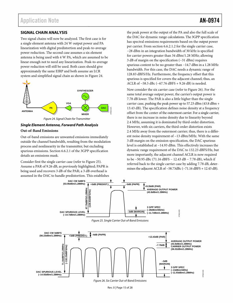
SIGNAL CHAIN ANALYSIS Two signal chains will now be analyzed. The first case is for a single element antenna with 24 W output power and PA linearization with digital predistortion and peak-to-average power reduction. The second case assumes a six element antenna is being used with 4 W PA, which are assumed to be linear enough not to need any linearization. Peak-to-average power reduction will still be used. Both cases should give approximately the same EIRP and both assume an LCR system and simplified signal chain as shown in Figure 24.
0766
3-02
4ANTENNA
DACPA
VGA
SYNTHESIZER
MIXER Figure 24. Signal Chain for Transmitter
Single Element Antenna, Forward Path Analysis
Out-of-Band Emissions
Out-of-band emissions are unwanted emissions immediately outside the channel bandwidth, resulting from the modulation process and nonlinearity in the transmitter, but excluding spurious emissions. Section 6.6.2.1 of the 3GPP specification details an emissions mask.
Consider first the single carrier case (refer to Figure 25). Assume a PAR of 9.26 dB, as previously highlighted; PAPR is being used and recovers 3 dB of the PAR; a 3 dB overhead is assumed in the DAC to handle predistortion. This establishes
the peak power at the output of the PA and also the full scale of the DAC for dynamic range calculations. The 3GPP specification has spectral emissions requirements based on the output power per carrier. From section 6.6.2.1.2 for the single carrier case, −28 dBm in an integration bandwidth of 30 kHz is specified for carrier powers greater than 34 dBm/1.28 MHz; allowing 3 dB of margin on the specification (−31 dBm) requires spurious content to be no greater than −14.7 dBm in a 1.28 MHz bandwidth. For this case, the DAC needs a dynamic range of 128.83 dBFS/Hz. Furthermore, the frequency offset that this spurious is specified for covers the adjacent channel; thus, an ACLR of −58.5 dBc (−67.76 dBFS + 9.26 dB) is needed.
Now consider the six carrier case (refer to Figure 26). For the same total average output power, the carrier’s output power is 7.78 dB lower. The PAR is also a little higher than the single carrier case, pushing the peak power up to 57.23 dBm (43.8 dBm + 13.43 dB). The specification defines noise density at a frequency offset from the center of the outermost carrier. For a single carrier, there is no increase in noise density due to linearity beyond 2.4 MHz, assuming it is dominated by third-order distortion. However, with six carriers, the third-order distortion exists 2.4 MHz away from the outermost carrier; thus, there is a differ-ent noise density requirement of −13 dBm/MHz. With the same 3 dB margin on the emission specification, the DAC spurious level is established at −14.93 dBm. This effectively increases the dynamic range requirement of the DAC to 132.23 dBFS/Hz, but more importantly, the adjacent channel ACLR is now required to be −50.95 dBc (71.16 dBFS − 12.43 dB − 7.78 dB), which if referred back to the single carrier case by adding 7.78 dB, deter-mines the adjacent ACLR of −58.73dBc (−71.16 dBFS + 12.43 dB).
–3dB (PAPR)
–3dB (MARGIN)
+3dB (PREDIST.)
67.7
6dB
FS/1
.28M
Hz
(128
.83d
BFS
/Hz)
DAC CW 0dBFS(53.06dBm/1.28MHz)
DAC SPURIOUS LEVEL(–14.7dBm/1.28MHz)
+9.26dB (PAR)AVERAGE OUTPUT POWER(43.8dBm/1.28MHz)
3 GPP SPEC(–28dBm/30kHz)
0766
3-02
5
(–11.7dBm/1.28MHz)
Figure 25. Single Carrier Out-of-Band Emissions
–4dB (PAPR)
–3dB(MARGIN)
+3dB (PREDIST.)
71.1
6dB
FS/1
.28M
Hz
(–13
2.23
dBFS
/Hz)
DAC CW 0dBFS(56.23dBm/1.28MHz)
DAC SPURIOUS LEVEL(–14.93dBm/1.28MHz)
+13.43dB (PAR)
–7.78dBAVERAGE OUTPUT POWER(43.8dBm/1.28MHz)CARRIER OUTPUT POWER(36.02dBm/1.28MHz)
3 GPP SPEC(–13dBm/1MHz)
0766
3-02
6
(–11.93dBm/1.28MHz)
Figure 26. Six Carrier Out-of-Band Emissions

AN-0974 Application Note
Rev. 0 | Page 16 of 28
Spurious Emissions
This part of the specification broadly covers how the channel affects other radios, including this base station’s receiver. If a single carrier is placed at the band edge, as shown in Figure 27(1), there is a requirement for −30 dBm/MHz 10 MHz away from the carrier, using Category B emissions requirements. At this frequency offset, there is no influence from harmonics and any noise density would be due to broadband noise. If multiple car-riers are used, the −30 dBm/MHz requirement is still present, as shown in Figure 27(2), but in this case, it is possible that fifth-order distortion could pollute this band. However, if the system is dominated by third-order distortion, any noise energy at this frequency offset is due to broadband noise.
The single carrier case, Figure 28, has the same peak level as previously discussed; now there is a requirement of −30 dBm/MHz (−28.93 dBm/1.28 MHz), which, if the same 3 dB margin is used, requires no spurious be greater than −31.93 dBm/1.28 MHz. As this frequency offset is too close to the carrier for any filter transition band to be effective, this requirement sets the mini-mum broadband noise requirement and the ACLR requirement of the alternate channels to −75.73 dBc(−84.99 dBFS + 9.26 dB).
For the six carrier case (see Figure 29), the peak level is higher than the single carrier case, which when coupled with the low spurious requirement, sets a DAC minimum dynamic range requirement of −149.23 dBFS/Hz. This requirement also increases the six carrier alternate ACLR requirement −67.95 dBc (−88.16 dBFS + 7.78 dB + 12.43 dB).
Fc1–16MHz
Fc1 Fc2
Fu+10MHz
Tx BAND
–15dBm
–25dBm–30dBm
Fl–10MHz20
00.0
2002
.5
2005
.0
2007
.5
2010
.0
2012
.5
2015
.0
2017
.5
2020
.0
2022
.5
2025
.0
2027
.5
2030
.0
2032
.5
2035
.0
Fc1–16MHz
Fc1–19.2MHz Fc1
Fu+10MHz
Tx BAND
–15dBm
–25dBm–30dBm
2007
.5
2010
.0
2012
.5
2015
.0
2017
.5
2020
.0
2022
.5
2025
.0
2027
.5
2030
.0
2032
.5
2035
.0
(1) (2) 0766
3-02
7
Figure 27. Spurious Emissions Limits
–3dB (PAPR)
–3dB (MARGIN)
+3dB (PREDIST.)
84.9
9dB
FS/1
.28M
Hz
(146
.06d
BFS
/Hz)
DAC CW 0dBFS(53.06dBm/1.28MHz)
DAC SPURIOUS LEVEL(–31.93dBm/1.28MHz)
+9.26dB (PAR)AVERAGE OUTPUT POWER(43.8dBm/1.28MHz)
3 GPP SPEC(–30dBm/1MHz)
0766
3-02
8
(–28.93dBm/1.28MHz)
Figure 28. Single Carrier, Single Element Antenna Spurious Emissions
–4dB (PAPR)
–3dB(MARGIN)
+3dB (PREDIST.)
88.1
6dB
FS/1
.28M
Hz
(–14
9.23
dBFS
/Hz)
DAC CW 0dBFS(56.23dBm/1.28MHz)
DAC SPURIOUS LEVEL(–31.93dBm/1.28MHz)
+13.43dB (PAR)
–7.78dB
AVERAGE OUTPUT POWER(43.8dBm/1.28MHz)CARRIER OUTPUT POWER(36.02dBm/1.28MHz)
0766
3-02
9
3 GPP SPEC(–30dBm/1MHz)(–29.83dBm/1.28MHz)
Figure 29. Six Carrier, Single Element Antenna Spurious Emissions

Application Note AN-0974
Rev. 0 | Page 17 of 28
Forward Path Verification
The minimum adjacent channel ACLR requirements are set by the out-of-band emissions requirements. The six carrier requirement of −50.95 dBc can be referred back to a single carrier requirement by adding 7.78 dB; allowing 1 dB for the summation of broadband noise within the adjacent channel yields a requirement of −59.73 dBc adjacent channel ACLR for a single carrier. The alternate channel ACLR requirements are derived from the spurious emissions specifications. Here, the requirements are −75.73 dBc.
We assume that the six carriers are using the test model with different scrambling code and that the composite waveform has a PAR of 13.43 dB and that PAPR reduces the PAR to 9.43 dB. It is also assumed that PA linearization is being used, improving the OIP3 of the PA. If a mixer/modulator similar to the ADL5372 is used, its output channel power should be −13 dBm. Allocating 17 dB gain to the VGA requires a gain of 40 dB in the PA to deliver approximately +44 dBm from the output of the DAC. Commercially available PAs and VGAs with these characteristics exhibit a noise figure of around 3 dB. Calculating the cascaded OIP3 at the output of the PA gives +71.01 dBm; if the preceding stages are assumed distortion free, the cascaded OIP3 results in an adjacent channel ACLR due to intermodulation, of −59.69 dBc (the effect of broadband noise is small enough to not impact the adjacent channel ACLR).
To achieve the −75.73 dBc of alternate channel ACLR with the VGA and PA noise and gain, the total noise at the output of the mixer needs to be around −154.6 dBm/Hz. Distributing this noise budget equally among the DAC, mixer and synthesizer yields the −75.77 dBc alternate channel ACLR. The above level plan places the DAC full-scale output at −3.57 dBm, requiring a DAC dynamic range of −153.4dBFS/Hz.
Using this channel lineup, a PCDE of −41.47 dB and an EVM of 3.37% results exceeding the specification.
Single Element Antenna, PA Linearization Observation Path Analysis
The only requirements of the observation path are that it be more linear than the required antenna linearity and that the noise performance does not impede the linearity measurement. Figure 31 shows the six-carrier out-of-band emissions require-ments in black with the observation path requirements in red. The observation path linearity is made to have a 6 dB margin over the forward path linearity with the observation path’s noise being 6 dB below the observation path’s linearity requirement. With the above level plan, the average output power of 43.8 dBm needs to be attenuated to align with the observation path receiver ADC’s full scale. Using a fixed attenuation of 60 dB, which can be a combination of directional coupler attenuation of typically 40 dB and a 20 dB step attenuation, allows some gain in the RF section. A 9 dB gain in the RF section preceding the ADC puts the average output power at −7.2 dBm. Using a 2 V p-p diffe-rential ADC full scale and assuming a 200 Ω input impedance, the ADC has a full-scale input power of 4 dBm/7 dBm peak. Allowing for the forward path’s predistortion margin (3 dB) and peak-to-average ratio (9.43 dB) puts the peak signal into the observation path ADC at 5.23 dBm; this allows some margin for ADC compression effects.
The observation path’s measurement noise should be −88 dBm/Hz at the antenna (refer to Figure 32), resulting in a 26 dB noise figure requirement at the input to the mixer and a −139 dBm/Hz noise density at the input to the ADC. Positioning the ADC’s noise contribution 10 dB below the RF’s requires the ADC to have −149 dBm/Hz noise density. A full scale of 4 dBm yields an ADC noise density of −153 dBFS/Hz. Because noise is not being corrected for, the noise of the RF and the ADC can be averaged over many cycles, resulting in a relaxed noise require-ment on both the RF and the ADC by 3 × log2(Nav), where Nav is the number of samples averaged over.
0766
3-03
0
ANTENNADACPA
VGA
SYNTHESIZER
MIXER
OUTPUT POWERINPUT POWERGAINIIP3OIP3NF
OVERALL OIP3ACLR DUE TO IP3ACLR DUE TO NOISE
444
403575
3
OUTPUT POWERINPUT POWERGAINIIP3OIP3NF
4–131720373
71.01–59.69–75.77
OVERALL ACLR (ADJ)OVERALL ACLR (ALT)
–59.69–75.77
PA VGAOUTPUT POWERINPUT POWERGAINIIP3OIP3NSD
–13–13
01919
–157
MIXEROUTPUT POWERINPUT POWERGAINIIP3OIP3NSD (dBm/Hz) NSD
1.6MHz OFFSET
–13–13
02929
–157 –157
IMD3PAR OVERHEAD0dBFS (dBm)NSD (dBFS/Hz)
709.43
–3.57–153.4
DAC SYNTHESIZER
Figure 30. Forward Path Level Planning

AN-0974 Application Note
Rev. 0 | Page 18 of 28
–4dB (PAPR)
–3dB (MARGIN)
+3dB (PREDIST.)
70.9
dBFS
/1.2
8MH
z(–
132.
23dB
FS/H
z)
DAC CW 0dBFS(56.23dBm/1.28MHz)
OUT-OF-BAND LIMIT(–14.93dBm/1.28MHz)
SPURIOUS EMISSIONS LIMIT(–31.93dBm/1.28MHz)
+13.43dB (PAR)
–7.78dBAVERAGE OUTPUT POWER(43.8dBm/1.28MHz)CARRIER OUTPUT POWER(36.02dBm/1.28MHz)
3GPP SPEC(–13dBm/1MHz)
–26.93dBm/1.28MHz–88.00dBm/Hz
83.1
6dB
FS14
4.23
dBFS
/Hz
(–11.93dBm/1.28MHz)
0766
3-03
1
–64.73dBc ACLR (wrt SINGLE CARRIER)
–6dB MEASUREMENT LINEARITY
–6dB MEASUREMENT NOISE
–5dB
Figure 31. Requirement of DPD Measurement Loop
BPF ADC
0766
3-03
2
POWERAMPLIFIER
–88.00dBm/Hz
G =
–60
dB
NF = 26 + 3×log2(Nav)G = 9dB
OIP3 = +25.22dBm
NF = 25 + 3×log2(Nav)G = 0dB
OIP3 = +25.22dBm
–148
dBm
/Hz
–139
dBm
/Hz
DSP
NSD: –153dBFS/Hz + 3×log2(Nav)IMP: –72.84dBc @ –11.2dBFS
Figure 32. Observation Path Signal Chain
With the observation path’s linearity margin, referred to a single carrier, a single carrier adjacent ACLR of −64.73 dBc is required. This corresponds to an IP3 of +22.22 dBm at the input to the ADC. Splitting this equally between the RF and the ADC results in an IIP3 of +25.22 dBm for the ADC. The input to the ADC is at −7.2 dBm or −11.2 dBFS yielding a two-tone IMD of −72.84 dBc at −11.2 dBFS.
Depending on the observation path approach, the AD9230 is capable of sampling at 250 MSPS, or more conveniently at 245.76 MSPS, allowing a 122.88 MHz Nyquist zone. This Nyquist zone allows the six carriers’ 9.6 MHz signal bandwidth to be digitized with the third and fifth harmonic components, occupying a 48 MHz total bandwidth. The excess bandwidth over 48 MHz allows for a simple antialias filter. The AD9230 is capable of −78 dBc two-tone IMD at 140 MHz IF with two −7 dBFS signals so is easily suited to the above requirement. At 140 MHz IF, the AD9230 has an SNR of 63.5 dB; this is a noise density of −144.4 dBFS/Hz over the 122.88 MHz Nyquist band. Using the AD9230 requires at least eight samples to be averaged to yield a processing gain of 9 dB and drop the AD9230’s noise density below the −153 dBFS/Hz requirement.
Six Element Antenna, Forward Path Analysis
Out-of-Band Emissions
The 3GPP specification is written with reference to the antenna port, consequently a six element antenna, having six antenna ports and a sixth of the power of the single element antenna port has a different set of spectral requirements, even though the radiated power per user can be the same between the six element antenna and the single element antenna. The peak-to-average ratio of the signal will be the same between the two antenna configurations, although in the six-element antenna case it is assumed that PA linearization is not needed, so the margin for the linearization algorithm is removed. The peak signal out of the DAC is therefore at the 42.28 dBm/1.28 MHz level. For a single carrier’s per carrier power of 36.02 dBm (4 W) the same noise level as the 24 W case is specified; with the same 3 dB of margin over the specification a total dynamic range of 56.98 dBFS/1.28 MHz results and an adjacent channel ACLR of −50.72 dBc is needed. Refer to Figure 33.
For the six carrier case, the per carrier power is now 28.24 dBm, which has a different spectral requirement than the single carrier case. The spectral noise needs to be 47 dB below the carrier with a measurement bandwidth of 1 MHz, made with respect to a measurement on the carrier with a measurement bandwidth of

Application Note AN-0974
Rev. 0 | Page 19 of 28
1.28 MHz. This places a requirement of −17.69 dBm/1.28 MHz 2.4 MHz away from the outermost carrier. This raises the dynamic range requirement to 66.14 dBFS and requires an adjacent channel ACLR of −48.93 dBc, referred to a single carrier an adjacent channel ACLR of −56.71 dBc. Refer to Figure 34.
Spurious Emissions
Spurious emissions are not dependent upon power level, so the same Category B emissions that were used in the single element antenna case also apply to the six-element antenna case. Because
the average output power is lower in the six-element antenna case, the total dynamic range requirement is now significantly reduced to 74.21 dBFS/128 MHz. This sets an alternate channel ACLR of −67.95 dBc. Refer to Figure 35.
For the six carrier case (see Figure 36), the total dynamic range requirement is also significantly reduced, resulting in an alter-nate channel ACLR of −60.17 dBc, which would be −67.95 dBc when referred to a single carrier, not surprisingly the same as the single carrier case.
–3dB (PAPR)28
MH
zH
z)
DAC CW 0dBFS(42.28dBm/1.28MHz) +9.26dB (PAR)
AVERAGE OUTPUT POWER(36.02dBm/1.28MHz)
–3dB (MARGIN)
56.9
8dB
FS/1
.(1
18.0
5dB
FS/
DAC SPURIOUS LEVEL(–14.7dBm/1.28MHz)
3 GPP SPEC(–28dBm/30kHz)(–11.7dBm/1.28MHz)
0766
3-03
3
Figure 33. Single Carrier Out-of-Band Emissions
–4dB (PAPR)
66.1
4dB
FS/1
.28M
Hz
(–12
7.21
dBFS
/Hz)
P –4
7dB
/1M
Hz
3GPP
SPE
C
DAC CW 0dBFS(45.45dBm/1.28MHz)
DAC SPURIOUS LEVEL(–20.69dBm/1.28MHz)
+13.43dB (PAR)
–7.78dBAVERAGE OUTPUT POWER(36.02dBm/1.28MHz)CARRIER OUTPUT POWER(28.24dBm/1.28MHz)
(–17.69dBm/1.28MHz)
0766
3-03
4
–3dB (MARGIN)
Figure 34. Six Carriers Out-of-Band Emissions
–3dB (PAPR)
–3dB (MARGIN)
74.2
1dB
FS/1
.28M
Hz
(135
.28d
BFS
/Hz)
DAC CW 0dBFS(42.28dBm/1.28MHz)
DAC SPURIOUS LEVEL(–31.93dBm/1.28MHz)
+9.26dB (PAR)AVERAGE OUTPUT POWER(36.02dBm/1.28MHz)
3 GPP SPEC(–30dBm/1MHz)(–28.93dBm/1.28MHz)
0766
3-03
5
Figure 35. Single Carrier Spurious Emissions
–4dB (PAPR)
–3dB(MARGIN)77
.38d
BFS
/1.2
8MH
z(–
138.
45dB
FS/H
z)
DAC CW 0dBFS(45.45dBm/1.28MHz)
DAC SPURIOUS LEVEL(–31.93dBm/1.28MHz)
+13.43dB (PAR)
–7.78dBAVERAGE OUTPUT POWER(36.02dBm/1.28MHz)CARRIER OUTPUT POWER, P(28.24dBm/1.28MHz)
3 GPP SPEC(–30dBm/1MHz)(–29.83dBm/1.28MHz)
0766
3-03
6
Figure 36. Six Carrier Spurious Emissions

AN-0974 Application Note
Rev. 0 | Page 20 of 28
0766
3-03
7
Forward Path Verification
The adjacent channel ACLR requirement is set by the six car-rier out-of-band emissions requirement of −56.71 dBc and the alternate channel ACLR is the same between the single and six carrier case at −67.95 dBc. Using a similar approach as before,
with the IP3 of the PA relaxed by 10 dB as PA linearization is not being used, the signal chain is a more relaxed version of the single element antenna case.
ANTENNADACPA
VGA
SYNTHESIZER
MIXER
OUTPUT POWERINPUT POWERGAINIIP3OIP3NF
OVERALL OIP3ACLR DUE TO IPACLR DUE TO NO
36–44025653
OUTPUT POWERINPUT POWERGAINIIP3OIP3NF
–4–161215273
PA VGA
3ISE
61.41–56.48–67.77
OVERALL ACLR (ADJ)OVERALL ACLR (ALT)
–56.46–67.77
OUTPUT POWERINPUT POWERGAINIIP3OIP3NSD
–16–16
01515
–152
MIXEROUTPUT POWERINPUT POWERGAINIIP3OIP3NSD (dBm/Hz) NSD
1.6MHz OFFSET
–16–16
02929
–152 –152
IMD3 70
DAC SYNTHESIZER
PAR OVERHEAD0dBFS (dBm)NSD (dBFS/Hz)
9.43–6.57
–145.4 Figure 37. Forward Path Level Planning
Application Note AN-0974
Rev. 0 | Page 21 of 28
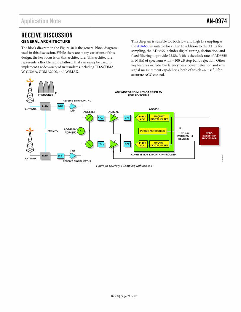
RECEIVE DISCUSSION GENERAL ARCHITECTURE The block diagram in the Figure 38 is the general block diagram used in this discussion. While there are many variations of this design, the key focus is on this architecture. This architecture represents a flexible radio platform that can easily be used to implement a wide variety of air standards including TD-SCDMA, W-CDMA, CDMA2000, and WiMAX.
This diagram is suitable for both low and high IF sampling as the AD6655 is suitable for either. In addition to the ADCs for sampling, the AD6655 includes digital tuning, decimation, and fixed filtering to provide 22.8% fs (fs is the clock rate of AD6655 in MHz) of spectrum with > 100 dB stop band rejection. Other key features include low latency peak power detection and rms signal measurement capabilities, both of which are useful for accurate AGC control.
ANTENNA
ANTENNA
FREQUENCY
AD8376ADL5355
LNA
ADF4106/ADF4350FROM Tx
RECEIVE SIGNAL PATH 1
RECEIVE SIGNAL PATH 2
BPF
BPFTx/Rx
14-BITADC
NYQUISTDIGITAL FILTER
POWER MONITORING
BPF
BPFTx/Rx
LNA
14-BITADC
NYQUISTDIGITAL FILTER
TO SPIENABLEDDEVICES
FPGABASEBAND
PROCESSOR
n
AD6655 IS NOT EXPORT CONTROLLED
0766
3-03
8
AD6655
ADI WIDEBAND MULTI-CARRIER RxFOR TD-SCDMA
Figure 38. Diversity IF Sampling with AD6655

AN-0974 Application Note
Rev. 0 | Page 22 of 28
In addition, the AD6655 is suitable for direct conversion (refer to Figure 39). Although direct conversion is difficult for multicarrier
TD-SCDMA, WCDMA and CDMA2000, it is quite suitable for WiMAX applications given that no subcarriers are placed at DC.
ADI WIDEBAND MULTI-CARRIER RxFOR TD-SCDMA (ALTERNATIVE)
0766
3-03
9
FREQUENCY
ANTENNA
AD8376ADL5382
ADF4106/ADF4350
RECEIVE SIGNAL PATH 1
LPF 14-BITADC
NYQUISTDIGITAL FILTER
POWER MONITORING
LPF
BPF
LNA
14-BITADC
NYQUISTDIGITAL FILTER
n
AD6655 IS NOT EXPORT CONTROLLED
AD6655
90°0°
ANTENNA
FREQUENCY
AD8376ADL5382
ADF4106/ADF4350
RECEIVE SIGNAL PATH 2 LPF 14-BITADC
NYQUISTDIGITAL FILTER
POWER MONITORING
AD6655
LPF
BPF
LNA
14-BITADC
NYQUISTDIGITAL FILTER
n
90°0°
I
Q
I
Q
FPGABASEBAND
PROCESSOR
AD6655 IS NOT EXPORT CONTROLLED
Figure 39. Diversity Baseband Sampling with the AD6655
Application Note AN-0974
Rev. 0 | Page 23 of 28
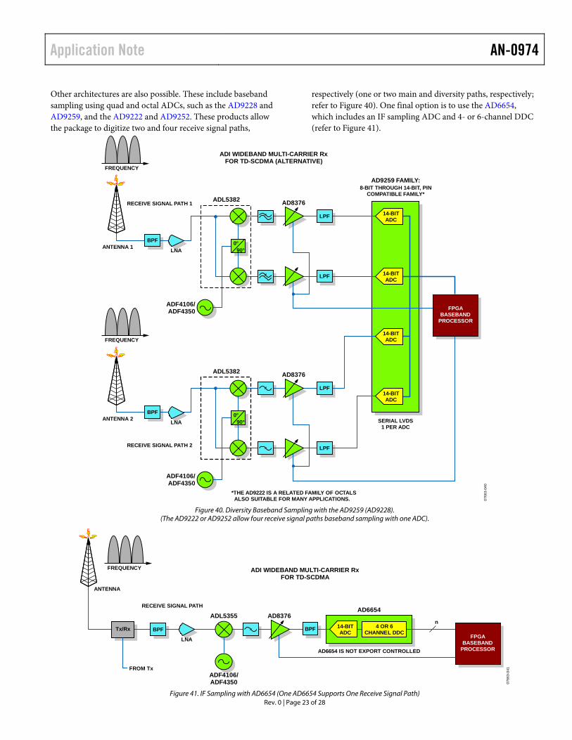
Other architectures are also possible. These include baseband sampling using quad and octal ADCs, such as the AD9228 and AD9259, and the AD9222 and AD9252. These products allow the package to digitize two and four receive signal paths,
respectively (one or two main and diversity paths, respectively; refer to Figure 40). One final option is to use the AD6654, which includes an IF sampling ADC and 4- or 6-channel DDC (refer to Figure 41).
0766
3-04
0
ANTENNA 1
FREQUENCY
AD8376ADL5382
ADF4106/ADF4350
RECEIVE SIGNAL PATH 1
LPF
LPF
BPF
LNA 90°0°
ANTENNA 2
FREQUENCY
AD8376ADL5382
ADF4106/ADF4350
RECEIVE SIGNAL PATH 2 LPF
LPF
BPF
LNA 90°0°
FPGABASEBAND
PROCESSOR
14-BITADC
14-BITADC
14-BITADC
14-BITADC
AD9259 FAMILY:8-BIT THROUGH 14-BIT, PIN
COMPATIBLE FAMILY*
SERIAL LVDS1 PER ADC
*THE AD9222 IS A RELATED FAMILY OF OCTALSALSO SUITABLE FOR MANY APPLICATIONS.
ADI WIDEBAND MULTI-CARRIER RxFOR TD-SCDMA (ALTERNATIVE)
Figure 40. Diversity Baseband Sampling with the AD9259 (AD9228).
(The AD9222 or AD9252 allow four receive signal paths baseband sampling with one ADC).
ANTENNA
FREQUENCY
AD8376ADL5355
ADF4106/ADF4350
RECEIVE SIGNAL PATH
LNA FPGABASEBAND
PROCESSOR
n
AD6654 IS NOT EXPORT CONTROLLED
AD6654
ADI WIDEBAND MULTI-CARRIER RxFOR TD-SCDMA
0766
3-04
1FROM Tx
4 OR 6CHANNEL DDC
14-BITADCTx/Rx BPFBPF
Figure 41. IF Sampling with AD6654 (One AD6654 Supports One Receive Signal Path)
AN-0974 Application Note
Rev. 0 | Page 24 of 28
Each of these solutions provides high levels of integration. Some solutions provide integration of multiple ADCs. Some provide integration of ADC and digital content. Others provide integra-tion of ADC and analog content. Still others, such as the AD6655, provide integration of both analog and digital content on the same chip. It is with that in mind that the discussion in the fol-lowing sections is offered. While the general discussion applies to the other configurations, only the AD6655 offers a compact, well-rounded integration solution. The other integration solu-tions may offer other benefits depending on the architectures.
RECEIVER REQUIREMENTS Specifications for this report are taken from the requirements for wide area base station (BS) as defined by 3GPP TS 25.105 V7.7.0, specifically Section 7. Key specifications from this standard are the reference sensitivities, band of deployment, and blocking requirements. It is assumed that the Node B terminal is not re-quired to meet the sensitivity and blocking requirements of different platforms at the same time. Meeting the sensitivity of a wide area BS while also matching the blocking requirements of the local area BS may be desirable, but is not the goal discussed here. It should be noted that the requirements of a Node B terminals for medium and local area BS have similar dynamic range requirements to the wide area version with the exception that the level planning is shifted up to account for the larger expected signal levels. These can be accommodated within the same design by shifting the level plans upward as these systems can also tolerate increased noise.
RECEIVER OPERATING CONDITIONS The standard specifies the following conditions:
• Static reference sensitivity is −110 dBm within a 1.28 MHz channel bandwidth. On a per hertz basis, this is a signal density of −171.1 dBm/Hz.
• Sensitivity with an adjacent channel present (1.6 MHz away) is reduced to −104 dBm with an adjacent channel power of −55 dBm.
• Sensitivity with a carrier beyond adjacent channel (3.2 MHz or greater away) is −104 dBm with a narrow-band CDMA blocker at −40 dBm.
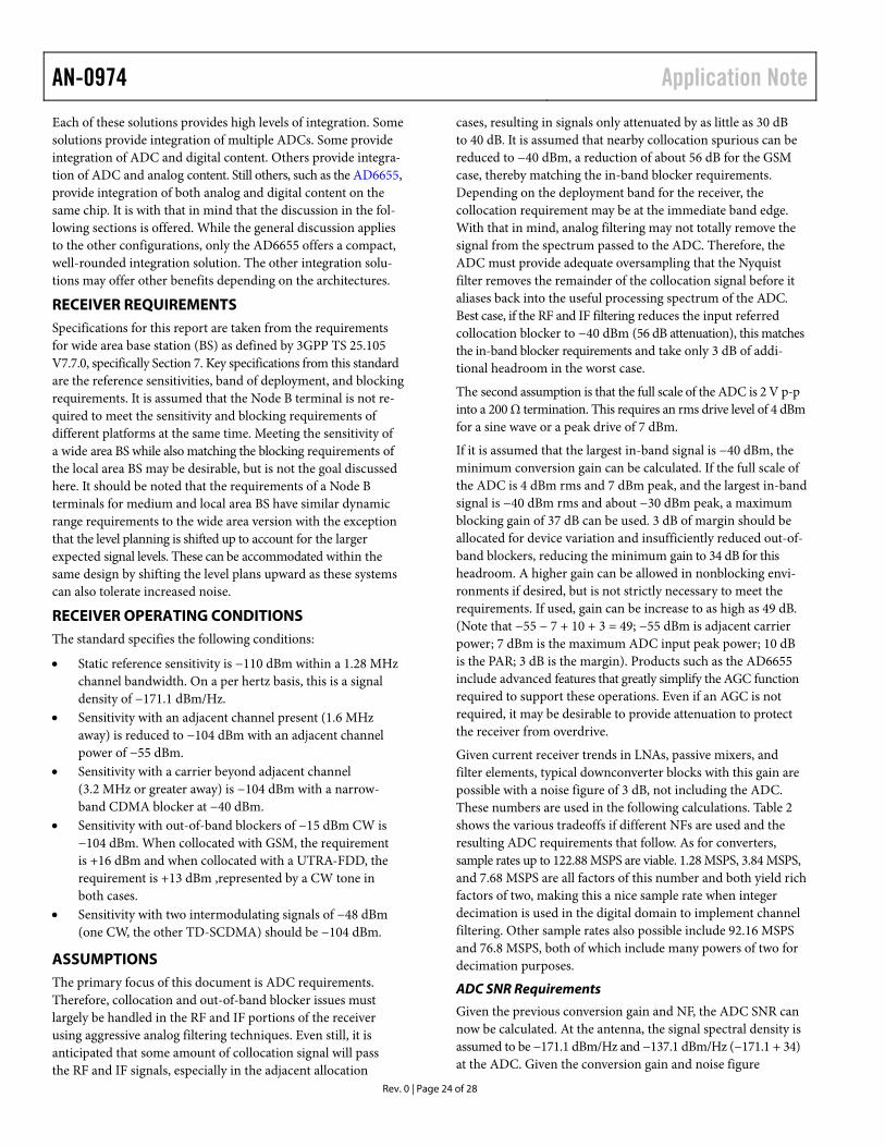
• Sensitivity with out-of-band blockers of −15 dBm CW is −104 dBm. When collocated with GSM, the requirement is +16 dBm and when collocated with a UTRA-FDD, the requirement is +13 dBm ,represented by a CW tone in both cases.
• Sensitivity with two intermodulating signals of −48 dBm (one CW, the other TD-SCDMA) should be −104 dBm.
ASSUMPTIONS The primary focus of this document is ADC requirements. Therefore, collocation and out-of-band blocker issues must largely be handled in the RF and IF portions of the receiver using aggressive analog filtering techniques. Even still, it is anticipated that some amount of collocation signal will pass the RF and IF signals, especially in the adjacent allocation
cases, resulting in signals only attenuated by as little as 30 dB to 40 dB. It is assumed that nearby collocation spurious can be reduced to −40 dBm, a reduction of about 56 dB for the GSM case, thereby matching the in-band blocker requirements. Depending on the deployment band for the receiver, the collocation requirement may be at the immediate band edge. With that in mind, analog filtering may not totally remove the signal from the spectrum passed to the ADC. Therefore, the ADC must provide adequate oversampling that the Nyquist filter removes the remainder of the collocation signal before it aliases back into the useful processing spectrum of the ADC. Best case, if the RF and IF filtering reduces the input referred collocation blocker to −40 dBm (56 dB attenuation), this matches the in-band blocker requirements and take only 3 dB of addi-tional headroom in the worst case.
The second assumption is that the full scale of the ADC is 2 V p-p into a 200 Ω termination. This requires an rms drive level of 4 dBm for a sine wave or a peak drive of 7 dBm.
If it is assumed that the largest in-band signal is −40 dBm, the minimum conversion gain can be calculated. If the full scale of the ADC is 4 dBm rms and 7 dBm peak, and the largest in-band signal is −40 dBm rms and about −30 dBm peak, a maximum blocking gain of 37 dB can be used. 3 dB of margin should be allocated for device variation and insufficiently reduced out-of-band blockers, reducing the minimum gain to 34 dB for this headroom. A higher gain can be allowed in nonblocking envi-ronments if desired, but is not strictly necessary to meet the requirements. If used, gain can be increase to as high as 49 dB. (Note that −55 − 7 + 10 + 3 = 49; −55 dBm is adjacent carrier power; 7 dBm is the maximum ADC input peak power; 10 dB is the PAR; 3 dB is the margin). Products such as the AD6655 include advanced features that greatly simplify the AGC function required to support these operations. Even if an AGC is not required, it may be desirable to provide attenuation to protect the receiver from overdrive.
Given current receiver trends in LNAs, passive mixers, and filter elements, typical downconverter blocks with this gain are possible with a noise figure of 3 dB, not including the ADC. These numbers are used in the following calculations. Table 2 shows the various tradeoffs if different NFs are used and the resulting ADC requirements that follow. As for converters, sample rates up to 122.88 MSPS are viable. 1.28 MSPS, 3.84 MSPS, and 7.68 MSPS are all factors of this number and both yield rich factors of two, making this a nice sample rate when integer decimation is used in the digital domain to implement channel filtering. Other sample rates also possible include 92.16 MSPS and 76.8 MSPS, both of which include many powers of two for decimation purposes.
ADC SNR Requirements
Given the previous conversion gain and NF, the ADC SNR can now be calculated. At the antenna, the signal spectral density is assumed to be −171.1 dBm/Hz and −137.1 dBm/Hz (−171.1 + 34) at the ADC. Given the conversion gain and noise figure
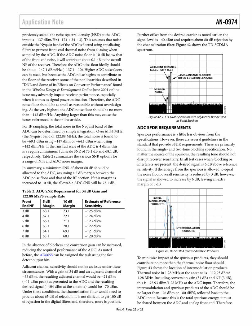
Application Note AN-0974
Rev. 0 | Page 25 of 28
previously stated, the noise spectral density (NSD) at the ADC input is −137 dBm/Hz (−174 + 34 + 3). This assumes that noise outside the Nyquist band of the ADC is filtered using antialiasing filters to prevent front-end thermal noise from aliasing when sampled by the ADC. If the ADC noise floor is 10 dB below that of the front-end noise, it will contribute about 0.1 dB to the overall NF of the receiver. Therefore, the ADC noise floor ideally should be about −147.1 dBm/Hz (−137.1 − 10). Higher ADC noise floors can be used, but because the ADC noise begins to contribute to the floor of the receiver, some of the nonlinearities described in “DNL and Some of its Effects on Converter Performance” found in the Wireless Design & Development Online June 2001 online issue may adversely impact receiver performance, especially when it comes to signal power estimation. Therefore, the ADC noise floor should be as small as reasonable without overdesign-ing. At the very highest, the ADC noise floor should be no more than −142 dBm/Hz. Anything larger than this may cause the issues referenced in the online article.
For IF sampling, the total noise in the Nyquist band of the ADC can be determined by simple integration. Over 61.44 MHz (the Nyquist band of 122.88 MHz), the total noise is found to be −69.1 dBm using −147 dBm or −64.1 dBm when using −142 dBm/Hz. If the rms full scale of the ADC is 4 dBm, this is a required minimum full scale SNR of 73.1 dB and 68.1 dB, respectively. Table 2 summarizes the various SNR options for a range of NFs and ADC noise margin.
In summary, a minimum SNR of about 68 dB should be allocated to the ADC, assuming a 5 dB margin between the ADC noise floor and that of the RF section. If this margin is increased to 10 dB, the allowable ADC SNR will be 73.1 dB.
Table 2. ADC SNR Requirement for 34 dB Gain and 122.88 MSPS Sample Rate Front End NF
5 dB Margin
10 dB Margin
Estimate of Reference Sensitivity
3 dB 68.1 73.1 −125 dBm 4 dB 67.1 72.1 −124 dBm 5 dB 66.1 71.1 −123 dBm 6 dB 65.1 70.1 −122 dBm 7 dB 64.1 69.1 −121 dBm 8 dB 63.1 68.1 −120 dBm
In the absence of blockers, the conversion gain can be increased, reducing the required performance of the ADC. As noted before, the AD6655 can be assigned the task using the fast detect output bits.
Adjacent channel selectivity should not be an issue under these circumstances. With a gain of 34 dB and an adjacent channel of −55 dBm, the resulting adjacent channel would be −21 dBm (−11 dBm peak) as presented to the ADC and the resulting desired signal (−104 dBm at the antenna) would be −70 dBm. Under these conditions, the channelization filter would need to provide about 65 dB of rejection. It is not difficult to get 100 dB of rejection in the digital filters and, therefore, more is possible.
Further offset from the desired carrier as noted earlier, the signal level is −40 dBm and requires about 80 dB rejection by the channelization filter. Figure 42 shows the TD-SCDMA spectrum.
–40dBm INBAND BLOCKEROR CO-LOCATION LEAKAGE
ADJACENT CHANNELSELECTIVITY TEST
DESIREDSIGNAL
0766
3-04
2
Figure 42. TD-SCDMA Spectrum with Adjacent Channel and
In-Band Blockers
ADC SFDR REQUIREMENTS Spurious performance is a little less obvious from the specifications. However, there are several guidelines in the standard that provide SFDR requirements. These are primarily found in the single- and two-tone blocking specification. No matter the source of the spurious, the resulting tone should not disrupt receiver sensitivity. In all test cases where blocking or interferers are present, the desired signal is 6 dB above reference sensitivity. If the energy from the spurious is allowed to equal the noise floor, overall sensitivity is reduced by 3 dB; however, the signal is allowed to increase by 6 dB, leaving an extra margin of 3 dB.
INTERMODULATIONPRODUCTS
INTER-MODULATIONPRODUCTS
0766
3-04
3
Figure 43. TD-SCDMA Intermodulation Products
To minimize impact of the spurious products, they should contribute no more than the thermal noise floor should. Figure 43 shows the location of intermodulation products. Thermal noise in 1.28 MHz at the antenna is −112.93 dBm/ 1.28 MHz. Including conversion gain (34 dB) and NF (3 dB), this is −75.93 dBm/1.28 MHz at the ADC input. Therefore, the intermodulation and spurious products of the ADC should be no larger than −76 dBm or −80 dBFS, reflected back to the ADC input. Because this is the total spurious energy, it must be shared between the ADC and analog front end. Therefore,

AN-0974 Application Note
Rev. 0 | Page 26 of 28
an additional 3 dB or more needs to be allocated to the ADC, bringing the total spurious performance of the ADC to −83 dBFS. This is the spurious performance required, regard less of the sources (SFDR, IMD, and other). Table 3 lists the required SNR and SFDR of the ADC.
Table 3. ADC Minimum Required Performance to Prevent ADC Nonlinearities from Disrupting Performance.
SNR Spurious (SFDR, IMD, and Other)
Minimum ADC Performance
68 dBFS min 83 dBFS min
COMMENTS ON GAIN, FIXED OR VARIABLE The case presented here indicates that fixed gain is possible for a TD-SCDMA implementation. Even if gain control is not needed, it may be desirable to implement protection from input clipping. Regardless of the need, the AD6655 can aid in both gain control and clip prevention by utilizing the fast detect bits of the converter. The fast detect bits function similarly to an overflow bit on a converter. The key difference is that they can be programmed to detect signals that peak between 0 dBFS and −30 dBFS in a logarithmic fashion. The latency on this function is only two clock cycles, reducing the delay and allowing fast response during signal peaking. The chip also includes a lower threshold detection and dwell time setting that detect when the envelop falls below a programmable level, allowing the gain to be increased after clipping. The latency on the lower threshold is longer and used in conjunction with the dwell time associated with the built-in hysteresis used to prevent remodulation of the signal (refer to Figure 44). In addition to the various level detec-tors that can be used for gain control, the chip includes a full
featured power measurement circuitry. This circuit can be used to measure the power of a main and diversity signal as well as the power of an I and Q signal. The power can be read through the SPI registers or through a dedicated high speed serial data inter-face (SMI port), making it a useful addition to applications that require tight power control of detected signals and full featured automatic gain control and power measurement systems.
VALIDATION Given a gain of 34 dB and an analog front end NF of 3 dB, what levels of performance can be expected? Additionally, what improvements can be made if gain is increased and decreased by 6 dB? Table 4shows how residual SNR and ADC clip point will change as a function system gain. It should be noted that spurious that fall in-band and have energy equal to the noise floor (-83 dBFS) will degrade performance by 3 dB. Sufficient margin exists to tolerate about 6 dB degradation from com-bined ADC and analog front end distortion plus noise generated from clock jitter and system phase noise. Refer to AN-501 and AN-756 for more information on system phase noise and clock jitter.
Table 4. ADC Clip Point as a Function of System Gain
Gain AFE NF
0 dB SNR for 1.28 MCPS
Effective SNR @ −110 dBm1
ADC Clip Point (CW Tone)
28 dB 6 dB −106.93 dBm −3.07 −24 dBm 34 dB 3 dB −109.93 dBm −0.07 −30 dBm 40 dB 3 dB −109.93 dBm −0.07 −36 dBm 1 Not including despreading factor. Despreading improves the SNR by the
despreading or processing gain
CO
NVE
RTE
R M
AG
NIT
UD
E IN
FOR
MAT
ION
DWELL TIME
TIMER RESET BYRISE ABOVE
F_LT
UPPE
TIMER COMPLETES BEFORESIGNAL RISES ABOVE F_LT
DWELL TIMEC_UT OR F_UT*
F_LT
DG
IG
*C_UT AND F_UT DIFFER ONLY IN ACCURACY AND LATENCY. SEE TEXT FOR MORE DETAILS.NOTES1. OUTPUTS FOLLOW THE INSTANTEOUS SIGNAL MAGNITUDE
AND NOT THE ENVELOP AND ARE GUARANTEED ACTIVE FOR A MINIMUM OF 2 ADC CLOCK CYCLES. 07
663-
044
FINE LOWER THRESHOLD
R THRESHOLD (COARSE OR FINE)
Figure 44. AD6655 Gain Control Features

Application Note AN-0974
Rev. 0 | Page 27 of 28
MARGIN FOR A SIX-CARRIER RECEIVER The assumption for this entire discussion has been that this is a wideband receiver and that the requirements in SNR and SFDR have been derived with that in mind. It is possible to trade off performance in these regards by adding analog channel filtering (SAW filters), but the specification here assumes no narrow-band filtering.
If six carriers are to be processed with this wideband receiver, the maximum level of each signal must be limited accordingly. With 34 dB of gain, the maximum rms input is −30 dBm rms. If five of the signals are −40 dBm, the total rms power is −33 dBm at the antenna, or about 1 dBm rms at the ADC input. Peaks are about 4 dB to 6 dB larger, depending on the peak-to-average profile, just under the clip point of the ADC at 7 dBm. If the sixth signal is the desired signal at some minimum level, it does not cause clipping of the ADC or signal chain. Assuming that the noise floor does not come up due to ADC behavior or phase noise of the synthesizers, a signal of −110 dBm is presented to the ADC at −76 dBm. Assuming a 3 dB noise figure from earlier discussion, the total noise in the channel bandwidth is −75.9 dB, resulting in roughly 0 dB SNR before despreading. Despreading
results in an SNR improvement of 20.2 dB. If 5 dB of SNR is needed, the minimum sensitivity is about 15 dB lower, or about −125 dBm. However, due to the nature of the large signals and phase noise, this number is likely a little worse, but on paper, it is achievable. In cases where additional large signals may be present, such as receivers with more than six carriers, it may be necessary to reduce conversion gain slightly. In these cases, reference sensitivity worsen 1 dB for each reduction in conversion gain. In addition, each dB reduction in conversion gain increases the SNR requirement by 1 dB as well, in order to prevent the ADC from dominating the receiver noise. While these test cases form a worst-case scenario, they do provide insight into the worst-case performance anticipated by such a receiver. By the standard and by practical application, conditions should be much easier. As such, a receiver designed to tolerate these input conditions should have few problems passing conformance testing. In summary, a TD-SCDMA receive chain can be built and can achieve superior sensitivity, even in blocking conditions, with a 12- to 14-bit ADC, including integrated devices such as the AD6655 and AD6654. This converter must have the specifications outlined in Table 3.

AN-0974 Application Note
Rev. 0 | Page 28 of 28
NOTES
©2008 Analog Devices, Inc. All rights reserved. Trademarks and registered trademarks are the property of their respective owners. AN07663-0-12/08(0)