Embed Size (px)
Citation preview

AMD 990FX/990X/970 BIOS Developer’s Guide
Technical Reference ManualRev. 3.00
P/N: 48694_990FX_990X_970_bdg_pub_3.00
© 2012 Advanced Micro Devices, Inc.

Trademarks
AMD, the AMD Arrow logo, ATI and combinations thereof are trademarks of Advanced Micro Devices, Inc.
HyperTransport is a licensed trademark of the HyperTransport Technology Consortium.
PCI Express and PCIe re registered trademarks of PCI-SIG (PCI Special Interest Group).
Other product names used in this publication are for identification purposes only and may be trademarks of their respective companies.
Disclaimer
The contents of this document are provided in connection with Advanced Micro Devices, Inc. ("AMD") products. AMD makes no representations or warranties with respect to the accuracy or completeness of the contents of this publication and reserves the right to make changes to specifications and product descriptions at any time without notice. No license, whether express, implied, arising by estoppel, or otherwise, to any intellectual property rights are granted by this publication. Except as set forth in AMD's Standard Terms and Conditions of Sale, AMD assumes no liability whatsoever, and disclaims any express or implied warranty, relating to its products including, but not limited to, the implied warranty of merchantability, fitness for a particular purpose, or infringement of any intellectual property right.
AMD's products are not designed, intended, authorized or warranted for use as components in systems intended for surgical implant into the body, or in other applications intended to support or sustain life, or in any other application in which the failure of AMD's product could create a situation where personal injury, death, or severe property or environmental damage may occur. AMD reserves the right to discontinue or make changes to its products at any time without notice.
© 2012 Advanced Micro Devices, Inc. All rights reserved.

Revision History
Date Revision Description
July 2012 3.00 - Re-issued as public version.- Replaced ASIC engineering codenames with
corresponding marketing names on the cover, and added correlation between the two in Section 1.1.
July 2010 1.00 First release
© 2012 Advanced Micro Devices, Inc. 48694 990FX/990X/970 BIOS Developer’s Guide 3.00

This page is left blank intentionally.
48694 990FX/990X/970 BIOS Developer’s Guide 3.00 © 2012 Advanced Micro Devices, Inc.

Table of Contents
Chapter 1: Introduction
1.1 About This Document .........................................................................................................................................................1-1
1.2 Architecture Overview ........................................................................................................................................................1-1
1.3 Differences amongst RD9xx Variants ................................................................................................................................1-1
Chapter 2: Register Space Access
2.1 PCIe® Core/Port Indirect Register Space (PCIEIND) .......................................................................................................1-1
2.2 PCIe Port Indirect Register Space (PCIEIND_P) ...............................................................................................................1-1
2.3 HTIU Indirect Register Space (HTIUIND) ........................................................................................................................1-1
2.4 MISC Indirect Register Space (MISCIND) ........................................................................................................................1-1
2.5 Clock Configuration Register Space (CLKCONFIG) ........................................................................................................1-2
Chapter 3: IRQ Mapping
3.1 Legacy Interrup Mapping (IO APIC Disabled) ..................................................................................................................1-1
3.2 I/O APIC Interrupt Mapping (I/O APIC 32 Entry Mode) ..................................................................................................1-2
3.3 I/O APIC Support................................................................................................................................................................1-2
Chapter 4: CIMx-RD9xx Architecture
4.1 Introduction .........................................................................................................................................................................1-1
4.2 Binary Image Design ..........................................................................................................................................................1-14.2.1 Binary Block Structure .........................................................................................................................................1-14.2.2 Binary Header.......................................................................................................................................................1-24.2.3 Module Header .....................................................................................................................................................1-2
4.3 Execution Environment Expectations .................................................................................................................................1-4
4.4 Standard Header ..................................................................................................................................................................1-4
4.5 Call Entry to Dispatcher......................................................................................................................................................1-5
4.6 Callback Function ...............................................................................................................................................................1-5
4.7 Operational Overview .........................................................................................................................................................1-6
4.8 Push-High Interface ............................................................................................................................................................1-74.8.1 Theory of Operation .............................................................................................................................................1-74.8.2 Making Calls to Image Entry Points ....................................................................................................................1-74.8.3 AmdBridge32 Procedure ......................................................................................................................................1-84.8.4 Handling Callback Procedures ...........................................................................................................................1-104.8.5 Alternative Callback in 32-Bit Mode ................................................................................................................. 1-11
4.9 Interface Calls ................................................................................................................................................................... 1-114.9.1 AmdInitializer..................................................................................................................................................... 1-114.9.2 AmdPowerOnResetInit....................................................................................................................................... 1-114.9.3 AmdHtInit........................................................................................................................................................... 1-114.9.4 AmdPcieEarlyInit ...............................................................................................................................................1-124.9.5 AmdEarlyPostInit ...............................................................................................................................................1-124.9.6 AmdMidPostInit .................................................................................................................................................1-124.9.7 AmdLatePostInit.................................................................................................................................................1-124.9.8 AmdS3Init ..........................................................................................................................................................1-13
4.10 Interface Callback ...........................................................................................................................................................1-134.10.1 AmdPortTrainingCompleted ..............................................................................................................................1-134.10.2 AmdPortResetDeassert.......................................................................................................................................1-14
© 2012 Advanced Micro Devices, Inc. 48694 990FX/990X/970 BIOS Developer’s Guide 3.00Table of Contents-1

Table of Contents
4.10.3 AmdPortResetAssert.......................................................................................................................................... 1-144.10.4 AmdPortResetSupported ................................................................................................................................... 1-154.10.5 AmdAllocateBuffer ........................................................................................................................................... 1-154.10.6 AmdFreeBuffer.................................................................................................................................................. 1-164.10.7 AmdGeneratePciReset ....................................................................................................................................... 1-164.10.8 AmdReportEvent ............................................................................................................................................... 1-174.10.9 AmdUpdateApicInterruptMapping.................................................................................................................... 1-174.10.10 AmdPcieAspmInfo ............................................................................................................................................ 1-18
4.11 Architectural Details of IOMMU ................................................................................................................................... 1-194.11.1 Theory of Operation .......................................................................................................................................... 1-194.11.2 Requirements ..................................................................................................................................................... 1-194.11.3 Execution ........................................................................................................................................................... 1-19
4.12 Legacy Wrapper Example ............................................................................................................................................. 1-19
Chapter 5: UEFI Support
5.1 UEFI Driver Information ................................................................................................................................................... 1-1
Chapter 6: Power Management
6.1 Sx State Power Management............................................................................................................................................. 1-16.1.1 Register Restoration............................................................................................................................................. 1-16.1.2 Resume from S3 State ......................................................................................................................................... 1-1
48694 990FX/990X/970 BIOS Developer’s Guide 3.00 © 2012 Advanced Micro Devices, Inc.Table of Contents-2

List of Figures
List of Figures
Figure 4-1: Binary Block Structure ................................................................................................................................................ 4-1Figure 4-2: Boot Sequence Flow-Chart ......................................................................................................................................... 4-5Figure 4-3: Push-High Interface ..................................................................................................................................................... 4-6Figure 4-4: Procedure Call through the Push-High Interface ........................................................................................................ 4-7Figure 4-5: Callout Router Operation ............................................................................................................................................ 4-8
© 2012 Advanced Micro Devices, Inc. 48694 990FX/990X/970 BIOS Developer’s Guide 3.00List of Figures-1

List of Figures
48694 990FX/990X/970 BIOS Developer’s Guide 3.00 © 2012 Advanced Micro Devices, Inc.List of Figures-2

List of Tables
List of Tables
Table 3-1: Legacy Interrupt Mapping .............................................................................................................................................3-1Table 3-2: I/O APIC Interrupt Mapping .........................................................................................................................................3-2
© 2012 Advanced Micro Devices, Inc. 48694 990FX/990X/970 BIOS Developer’s Guide 3.00List of Tables-1

List of Tables
48694 990FX/990X/970 BIOS Developer’s Guide 3.00 © 2012 Advanced Micro Devices, Inc.List of Tables-2

Chapter 1Introduction
1.1 About This Document
This manual contains guidelines for the BIOS and software development of a system that utilizes the AMD 990FX, AMD990X and AMD 970 northbridges. Note that throughout this document, the respective ASIC codenames RD990, RD980 and RX980 are used to designate the three variants. In addition, the abbreviation RD9xx is used to designate all three variants.
Changes and additions to the previous release of this document are highlighted in red. Refer to Revision History at the beginning of this document for change details.
1.2 Architecture Overview
The RD9xx is the system logic of the latest platform from AMD that enables its next generation CPUs with the leading ATI CrossFire™ solutions. The RD9xx has a total of up to 46 PCIe® lanes: 10 lanes are dedicated for external PCIe devices, and the rest support 2 x16 PCIe links or 4 x8 PCIe links for the ultimate graphics setup. With support for a four-lane A-Link Express III interface to AMD’s Southbridges such as the SB9xx, the RD9xx guarantees separate bandwidth for peripherals, graphics, and General Purpose Graphics Processor Unit (GPGPU). The RD9xx also comes equipped with the new HyperTransport™ 3 and PCIe Gen 2 technologies, with the ability for high system overclocking to deliver leadership performance. All of these are achieved by a highly integrated, thermally efficient design in a 29mm x 29mm package.
1.3 Differences amongst RD9xx Variants
The differences lie in the number of PCIe lanes supported.
The RD990 PCIe subsystem has 11 configurable PCIe ports that control in total 42 PCIe lanes, in addition to a 4-lane “A-Link Express III” with the Southbridge.
The RD980 PCIe subsystem has 8 configurable PCIe ports that control in total 22 PCIe lanes, in addition to a 4-lane “A-Link Express III” with the Southbridge.
The RX980 PCIe subsystem has 7 configurable PCIe ports that control in total 22 PCIe lanes, in addition to a 4-lane “A-Link Express III” with the Southbridge.
For more details, refer to the AMD RD9xx Databook.
© 2012 Advanced Micro Devices, Inc. 48694 990FX/990X/970 BIOS Developer’s Guide 3.001-1

Differences amongst RD9xx Variants
This page is left blank intentionally.
48694 990FX/990X/970 BIOS Developer’s Guide 3.00 © 2012 Advanced Micro Devices, Inc.1-2

Chapter 2Register Space Access
2.1 PCIe® Core/Port Indirect Register Space (PCIEIND)
The Core Index Space contains control and status registers that are generic to all PCIe ports in the RD9xx. This register space is accessed through the following index/data register pair located in the RD9xx’s northbridge PCI configuration registers:
• Index register is bus 0, device 0, register 0xE0.
• Data register is bus 0, device 0, register 0xE4.
Note: Register descriptions are referenced with the name PCIEIND.
The Core Index Space is subdivided into two parts. Since there are a total of 5 PCIe® cores in the RD9xx, hardware has been implemented to provide a mechanism to access these registers either independently or jointly through the programming of bits [18:16] of the index register 0xE0. The encoding is as follows:
• 0xE0[18:16] == 0x5: Reads and writes accesses to 0xE4 will be directed at the per-core index registers in PCIE-SB only.
• 0xE0[18:16] == 0x4: Reads and writes accesses to 0xE4 will be directed at the per-core index registers in PCIE-GFX only.
• 0xE0[18:16] == 0x6: Reads and writes accesses to 0xE4 will be directed at the per-core index registers in PCIE-GFX2 only.
• 0xE0[18:16] == 0x7: Reads and writes accesses to 0xE4 will be directed at the per-core index registers in PCIE-GPP only.
• 0xE0[18:16] == 0x3: Reads and writes accesses to 0xE4 will be directed at the per-core index registers in PCIE-GPP2 only.
Note: Register descriptions are referenced with the name PCIEIND or BIFNB.
2.2 PCIe Port Indirect Register Space (PCIEIND_P)
This register space is accessed through the following index/data register pair located in the RD9xx’s northbridge PCI configuration registers:
• Index register is bus 0, device 2/3/4/5/6/7/9/10/11/12/13, register 0xE0[15..0].
• Data register is bus 0, device 2/3/4/5/6/7/9/10/11/12/13, register 0xE4[31..0].
Note: Register descriptions are referenced with the name PCIEIND_P or BIFNBP.
2.3 HTIU Indirect Register Space (HTIUIND)
This register space is accessed through the following index/data register pair located in the RD9xx’s northbridge PCI configuration registers:
• Index register is bus 0, device 0, register 0x94[7..0].
• Data register is bus 0, device 0, register 0x98[31..0]. To write HTIUIND, register 0x94[8] has to be set.
Note: Register descriptions are referenced with the name HTIUIND.
2.4 MISC Indirect Register Space (MISCIND)
This register space is accessed through the following index/data register pair located in the RD9xx’s northbridge PCI configuration registers:
• Index register is bus 0, device 0, register 0x60[7..0].
© 2012 Advanced Micro Devices, Inc. 48694 990FX/990X/970 BIOS Developer’s Guide 3.002-1

Clock Configuration Register Space (CLKCONFIG)
• Data register is bus 0, device 0, register 0x64[31..0]. To write MISCIND, register 0x60[7] has to be set.
Note: Register descriptions are referenced with the name MISCIND.
2.5 Clock Configuration Register Space (CLKCONFIG)
The RD9xx clock control block is located in Device0, Function1. By default, this PCI function does not appear in the PCI configuration space. System firmware can make Device0, Function1 visible by setting NBCONFIG:0x4C[0] to 1. The expected use of the Clock Control function is to only enable it in the PCI configuration space for modification by system firmware during POST. This function does not implement PCI device and vendor ID’s. Therefore, system firmware should hide the Clock Control function after making modifications.
48694 990FX/990X/970 BIOS Developer’s Guide 3.00 © 2012 Advanced Micro Devices, Inc.2-2

Chapter 3IRQ Mapping
3.1 Legacy Interrup Mapping (IO APIC Disabled)
Table 3-1 Legacy Interrupt Mapping
Device Behind Internal Bridge # Interrupt Mapping INT_SEL_MODE == 1 Interrupt Mapping
2
INTA -> INTCINTB -> INTDINTC -> INTAINTD -> INTB
INTA -> INTGINTB -> INTHINTC -> INTEINTD -> INTF
3
INTA -> INTDINTB -> INTAINTC -> INTBINTD -> INTC
INTA -> INTHINTB -> INTEINTC -> INTFINTD -> INTG
4
INTA -> INTAINTB -> INTBINTC -> INTCINTD -> INTD
INTA -> INTEINTB -> INTFINTC -> INTGINTD -> INTH
5
INTA -> INTBINTB -> INTCINTC -> INTDINTD -> INTA
INTA -> INTFINTB -> INTGINTC -> INTHINTD -> INTE
6
INTA -> INTCINTB -> INTDINTC -> INTAINTD -> INTB
INTA -> INTGINTB -> INTHINTC -> INTEINTD -> INTF
7
INTA -> INTDINTB -> INTAINTC -> INTBINTD -> INTC
INTA -> INTHINTB -> INTEINTC -> INTFINTD -> INTG
9
INTA -> INTBINTB -> INTCINTC -> INTDINTD -> INTA
INTA -> INTFINTB -> INTGINTC -> INTHINTD -> INTE
10
INTA -> INTCINTB -> INTDINTC -> INTAINTD -> INTB
INTA -> INTGINTB -> INTHINTC -> INTEINTD -> INTF
11
INTA -> INTDINTB -> INTAINTC -> INTBINTD -> INTC
INTA -> INTHINTB -> INTEINTC -> INTFINTD -> INTG
12
INTA -> INTAINTB -> INTBINTC -> INTCINTD -> INTD
INTA -> INTEINTB -> INTFINTC -> INTGINTD -> INTH
13
INTA -> INTBINTB -> INTCINTC -> INTDINTD -> INTA
INTA -> INTFINTB -> INTGINTC -> INTHINTD -> INTE
© 2012 Advanced Micro Devices, Inc. 48694 990FX/990X/970 BIOS Developer’s Guide 3.003-1

I/O APIC Interrupt Mapping (I/O APIC 32 Entry Mode)
3.2 I/O APIC Interrupt Mapping (I/O APIC 32 Entry Mode)
Default interrupt mapping setup by CIMx and can be overridden through dedicated interface callback.
3.3 I/O APIC Support
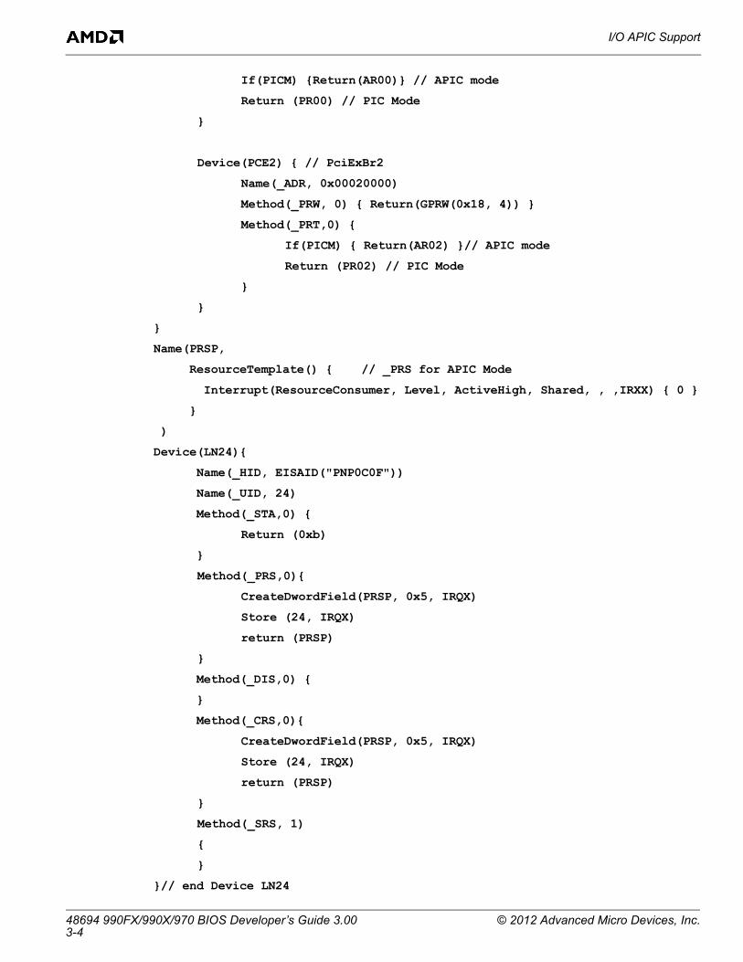
All RD9xx I/O APIC “Level Triggered” interrupt must be reported as Active High. Below is an example of I/O APIC interrupt routing implementation for ACPI for bridge device number 2. (LNKA/LNKB/LINKC/LINKD are SB interrupt link control devices, interrupt vector on RD9xx I/O APIC starts from 24).
//---------------------------------------------------------------
Table 3-2 I/O APIC Interrupt Mapping
Bridge Device Number Bridge Interrupt PinBridge IO APIC
Interrupt Pin Device Behind Bridge
Interrupt PinDevice Behind Bridge IO
APIC Interrupt Pin
2 INTA -> INTE INTA ->28
INTA -> INTAINTB -> INTBINTC -> INTCINTD -> INTD
INTA -> 0INTB -> 1INTC -> 2INTD -> 3
3 INTA -> INTE INTA ->28
INTA -> INTEINTB -> INTFINTC -> INTGINTD -> INTH
INTA -> 4INTB -> 5INTC -> 6INTD -> 7
4 INTA -> INTE INTA ->28
INTA -> INTEINTB -> INTFINTC -> INTGINTD -> INTH
INTA -> 20INTB -> 21INTC -> 22INTD -> 23
5 INTA ->INTE INTA ->28
INTA -> INTGINTB -> INTHINTC -> INTEINTD -> INTF
INTA -> 22INTB -> 23INTC -> 20INTD -> 21
6 INTA -> INTF INTA ->29
INTA -> INTDINTB -> INTAINTC -> INTBINTD -> INTC
INTA -> 27INTB -> 24INTC -> 25INTD -> 26
7 INTA -> INTF INTA ->29
INTA -> INTCINTB -> INTDINTC -> INTAINTD -> INTB
INTA -> 26INTB -> 27INTC -> 24INTD -> 25
9 INTA ->INTF INTA ->29
INTA -> INTAINTB -> INTBINTC -> INTCINTD -> INTD
INTA -> 24INTB -> 25INTC -> 26INTD -> 27
10 INTA -> INTG INTA -> 30
INTA -> INTHINTB -> INTEINTC -> INTFINTD -> INTG
INTA -> 23INTB -> 20INTC -> 21INTD -> 22
11 INTA -> INTG INTA -> 30
INTA -> INTAINTB -> INTBINTC -> INTCINTD -> INTD
INTA -> 8INTB -> 9
INTC -> 10INTD -> 11
12 INTA -> INTG INTA -> 30
INTA -> INTEINTB -> INTFINTC -> INTGINTD -> INTH
INTA -> 12INTB -> 13INTC -> 14INTD -> 15
13 INTA -> INTG INTA -> 30
INTA -> INTAINTB -> INTBINTC -> INTCINTD -> INTD
INTA -> 16INTB -> 17INTC -> 18INTD -> 19
48694 990FX/990X/970 BIOS Developer’s Guide 3.00 © 2012 Advanced Micro Devices, Inc.3-2

I/O APIC Support
// Begin System Bus Scope
//---------------------------------------------------------------
Scope(\_SB) {
// PciExBr2
Package(){0x0002FFFF, 0, LNKC, 0 },
...
}
Name(AR00, Package(){
// PciExBr2
Package(){0x0002FFFF, 0, LN52, 0 },
...
})
Name(PR02, Package(){
// PciExSlot2
Package(){0x0000FFFF, 0, LNKC, 0 },
Package(){0x0000FFFF, 1, LNKD, 0 },
Package(){0x0000FFFF, 2, LNKA, 0 },
Package(){0x0000FFFF, 3, LNKB, 0 },
...
})
Name(AR02, Package(){
// PciExSlot2
Package(){0x0000FFFF, 0, LN24, 0 },
Package(){0x0000FFFF, 1, LN25, 0 },
Package(){0x0000FFFF, 2, LN26, 0 },
Package(){0x0000FFFF, 3, LN27, 0 }
...
})
}
/---------------------------------------------------------------------
// Begin PCI tree object scope
//--------------------------------------------------------------------
Device(PCI0) {
Name(_HID, EISAID("PNP0A03"))
Name(_ADR, 0x00180000)
Method(^BN00, 0){ return(0x0000) }
Method(_BBN, 0){ return(BN00()) }
Name(_UID, 0x0000)
Method(_PRT,0) {
© 2012 Advanced Micro Devices, Inc. 48694 990FX/990X/970 BIOS Developer’s Guide 3.003-3
I/O APIC Support
If(PICM) {Return(AR00)} // APIC mode
Return (PR00) // PIC Mode
}
Device(PCE2) { // PciExBr2
Name(_ADR, 0x00020000)
Method(_PRW, 0) { Return(GPRW(0x18, 4)) }
Method(_PRT,0) {
If(PICM) { Return(AR02) }// APIC mode
Return (PR02) // PIC Mode
}
}
}
Name(PRSP,
ResourceTemplate() { // _PRS for APIC Mode
Interrupt(ResourceConsumer, Level, ActiveHigh, Shared, , ,IRXX) { 0 }
}
)
Device(LN24){
Name(_HID, EISAID("PNP0C0F"))
Name(_UID, 24)
Method(_STA,0) {
Return (0xb)
}
Method(_PRS,0){
CreateDwordField(PRSP, 0x5, IRQX)
Store (24, IRQX)
return (PRSP)
}
Method(_DIS,0) {
}
Method(_CRS,0){
CreateDwordField(PRSP, 0x5, IRQX)
Store (24, IRQX)
return (PRSP)
}
Method(_SRS, 1)
{
}
}// end Device LN24
48694 990FX/990X/970 BIOS Developer’s Guide 3.00 © 2012 Advanced Micro Devices, Inc.3-4

I/O APIC Support
Device(LN25){
Name(_HID, EISAID("PNP0C0F"))
Name(_UID, 25)
Method(_STA,0) {
Return (0xb)
}
Method(_PRS,0){
CreateDwordField(PRSP, 0x5, IRQX)
Store (25, IRQX)
return (PRSP)
}
Method(_DIS,0) {
}
Method(_CRS,0){
CreateDwordField(PRSP, 0x5, IRQX)
Store (25, IRQX)
return (PRSP)
}
Method(_SRS, 1)
{
}
}// end Device LN25
Device(LN26){
Name(_HID, EISAID("PNP0C0F"))
Name(_UID, 26)
Method(_STA,0) {
Return (0xb)
}
Method(_PRS,0){
CreateDwordField(PRSP, 0x5, IRQX)
Store (26, IRQX)
return (PRSP)
}
Method(_DIS,0) {
}
Method(_CRS,0){
CreateDwordField(PRSP, 0x5, IRQX)
Store (26, IRQX)
© 2012 Advanced Micro Devices, Inc. 48694 990FX/990X/970 BIOS Developer’s Guide 3.003-5

I/O APIC Support
return (PRSP)
}
Method(_SRS, 1)
{
}
}// end Device LN26
Device(LN27){
Name(_HID, EISAID("PNP0C0F"))
Name(_UID, 27)
Method(_STA,0) {
Return (0xb)
}
Method(_PRS,0){
CreateDwordField(PRSP, 0x5, IRQX)
Store (27, IRQX)
return (PRSP)
}
Method(_DIS,0) {
}
Method(_CRS,0){
CreateDwordField(PRSP, 0x5, IRQX)
Store (27, IRQX)
return (PRSP)
}
Method(_SRS, 1)
{
}
}// end Device LN27
Device(LN52){
Name(_HID, EISAID("PNP0C0F"))
Name(_UID, 52)
Method(_STA,0) {
Return (0xb)
}
Method(_PRS,0){
CreateDwordField(PRSP, 0x5, IRQX)
48694 990FX/990X/970 BIOS Developer’s Guide 3.00 © 2012 Advanced Micro Devices, Inc.3-6
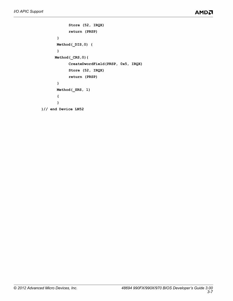
I/O APIC Support
Store (52, IRQX)
return (PRSP)
}
Method(_DIS,0) {
}
Method(_CRS,0){
CreateDwordField(PRSP, 0x5, IRQX)
Store (52, IRQX)
return (PRSP)
}
Method(_SRS, 1)
{
}
}// end Device LN52
© 2012 Advanced Micro Devices, Inc. 48694 990FX/990X/970 BIOS Developer’s Guide 3.003-7

I/O APIC Support
48694 990FX/990X/970 BIOS Developer’s Guide 3.00 © 2012 Advanced Micro Devices, Inc.3-8

Chapter 4CIMx-RD9xx Architecture
4.1 Introduction
The CIMx-RD9xx uses an interface and distribution model to help quickly integrate RD9xx northbridge family support in the customer products.
4.2 Binary Image Design
The binary image build style has several advantages and is required by the legacy Push-High interface. The binary image is compiled and built using 32-bit tools, while the legacy code uses 16-bit tools.
4.2.1 Binary Block Structure
CIMx software binary image is prefixed with a binary header which identifies the binary and points to the code module(s) contained within. There may be only a single code module or several modules combined into one binary image to reduce build overhead costs.
Figure 4-1 Binary Block Structure
The host environment must first find the binary image in the memory space, then calculate the execution address of the dispatcher to transfer control to the desired CIMx software function. Due to system requirements, the CIMx software may be spread out into three binary images. A typical legacy environment may choose to create the following images:
Image ‘B1’: A code image for use in recovery mode. This is a separate image to satisfy the requirement that the recovery code must be contained in a locked portion of the Flash ROM device.
Image ‘B2’: The main code image used during power-on initialization.
Image ‘B3’: A code image for use in system management mode. This is a separate image to allow a code load into SMM RAM for faster execution.
© 2012 Advanced Micro Devices, Inc. 48694 990FX/990X/970 BIOS Developer’s Guide 3.004-1

Binary Image Design
4.2.2 Binary Header
The following binary header exists in each binary image. It is the first element in the binary image and can be discovered by either implicit build knowledge or by searching the memory space for the signature constant. The binary image, and therefore the signature, must be aligned on a 32K byte boundary in the memory address space.
Prototype:
typedef struct {
UINT32 Signature; CHAR8 CreatorID[8]; CHAR8 Version[12]; UINT32 ModuleInfoOffset; UINT32 EntryPointAddress; UINT32 ImageBase; UINT32 RelocTableOffset; UINT32 ImageSize; UINT16 Checksum; UINT8 ImageType; UINT8 V_reserved;
} AMD_IMAGE_HEADER;
The parameters are defined as follows:
4.2.3 Module Header
A module header exists for each code module included in the binary image. There may be more than one module, in which case the NextBlock parameter is used to chain the modules in the binary image.
Prototype:
typedef struct _AMD_MODULE_HEADER {
UINT32 ModuleHeaderSignature, CHAR8 ModuleIdentifier[8], CHAR8 ModuleVersion[12], VOID *ModuleDispatcher, struct _AMD_MODULE_HEADER *NextBlock
Parameter Definition
Signature Signature that identifies this as an AGESA software image. This is a constant value equal to the string “$AMD”.
Creator ID Image creator ID signature. This is specified by a parameter and set by the BINUTIL image editing tool during the build process. It is set to <TBD> by the binary table editor tool.
Version Release version of binary image.
ModuleInfoOffset Offset of first occurrence of AmdModuleHeader relative to the start of the binary image.
EntryPointAddress Offset of the entry point relative to the start of the binary image.
ImageBase Image base address. This the linear/physical address to which the image code has presently been located (where it expects to execute).
RelocTableOffset Offset of relocation table, if applicable. Set to 0 if table not present. This the offset relative to the start of the binary image.
ImageSize Size, in bytes, of the complete binary image including the header.
Checksum Checksum of the binary image. The entire binary image sums to 0. Using a word summation of bytes style algorithm.
ImageType Image type, e.g. 1 – B1, 2 – B2, 3 – B3.
V_Reserved Must be 0.
48694 990FX/990X/970 BIOS Developer’s Guide 3.00 © 2012 Advanced Micro Devices, Inc.4-2

Binary Image Design
} AMD_MODULE_HEADER;
© 2012 Advanced Micro Devices, Inc. 48694 990FX/990X/970 BIOS Developer’s Guide 3.004-3

Execution Environment Expectations
The parameters are defined as follows:
4.3 Execution Environment Expectations
The image code expects to be located at an address determined by the host environment. This means the relocation fix-up records are used to fix-up the code references to addresses in the image. AMD provides a tool called BINUTIL2.EXE to perform this action. See “Build Process” in CIMX-NB.CHM.
Prior to calling any AGESA software interface, it is required that the host environment establish the following requirements:
• CPU is in 32-bit protected mode execution
• CS is a 32-bit code segment with Base/Limit – 0x00000000/0xffffffff.
• DS/ES/SS are 32-bit data segments with Base/Limit – 0x00000000/0xffffffff.
• If paging is enabled, then pages must be identity mapped (e.g.: pg 1 to pg1, pg 2 to pg2, etc)
4.4 Standard Header
An architectural header is defined at the front of every function’s configuration block. This standard header is filled by the host environment prior to calling through the entry point. This data is present in the configuration block at all times, essentially making it global throughout the function call. For example, this data is a part of the legacy Push-High.
Prototype:
typedef struct {
UINT32 ImageBasePtr; UINT32 Func; UINT32 AltImageBasePtr; VOID *PcieBasePtr; CALLOUT_ENTRY *CalloutPtr; UINT32 Reserved[3];
} AMD_CONFIG_PARAMS;
The parameters are defined as follows:
Parameter Definition
ModuleHeaderSignature Constant value equal to the string “$MOD”.
ModuleIdentifier Published name for this module.
ModuleVersion Release version of the module in string format.
ModuleDispatcher Offset of the module dispatcher relative to the start of the binary image.
NextBlock Offset of the next AmdModuleInfoBlock relative to the start of the binary image. If no more blocks are present, this is set to 0x00000000.
Parameter Definition
ImageBasePtr Memory location where the host environment has placed the binary image.
Func Identifier of the desired procedure. The identifiers are defined in a provided Include file.
AltImageBasePtr Memory location where the host environment has placed the B2 binary image. This value is optional and should be set to 0x00000000 when not used.
PcieBasePtr Base address of the memory mapped I/O block for access to PCIe configuration cycles.
CalloutPtr 32-bit pointer to where the host environment has placed the entry point for call-out routines. The AGESA software code transfers control to this address for processing of call-out functions (see section 4.6“Callback Function” on page 4-5). In a legacy Push-High environment this is the address of AmdCallout16.
Reserved Reserved for future use.
48694 990FX/990X/970 BIOS Developer’s Guide 3.00 © 2012 Advanced Micro Devices, Inc.4-4
Call Entry to Dispatcher
4.5 Call Entry to Dispatcher
The dispatcher in the code module uses a function definition as shown below. The value of the pointer ImageEntryPtr is determined by either implicit knowledge of the host build environment or by scanning the memory address space for the binary image.
Prototype:
AGESA_STATUS (*ImageEntryPtr) (
IN OUT AMD_NB_CONFIG_BLOCK *ConfigPtr
);
where ConfigPtr is a pointer to the function’s data structure which contains the standard header at the front (see CIMx-NB.CHM for detailed definition of AMD_NB_CONFIG_BLOCK structure).
Possible return values are:
4.6 Callback Function
All callback functions use the CallOutPtr structure element provided by the host environment in the Standard Header. The Callback function definition is as follows:
Prototype:
AGESA_STATUS (*CallBackPtr) (
IN UINT32 CallbackId,IN UINTN Data,IN OUT AMD_NB_CONFIG_BLOCK *ConfigPtr
);
The parameters are defined as follows:
Possible return values are:
Return Value Definition
AGESA_SUCCESS The selected function has competed successfully.
AGESA_UNSUPPORTED The selected function is not supported/implemented.
AGESA_ERROR The selected function signaled error.
AGESA_FATAL Non-recoverable error encountered during call. BIOS post should stop.
AGESA_WARNING Warning encountered during call.
Parameter Definition
CallbackId Identifier of the desired procedure. The identifiers are defined in a provided Include file.
Data Specific to callback data.
ConfigPtr Pointer to the function’s data structure which contains the Standard Header at the front. Refer to CIMX_NB.CHM for detailed definition of AMD_NB_CONFIG_BLOCK structure.
Return Value Definition
AGESA_SUCCESS The selected function has competed successfully.
AGESA_UNSUPPORTED The selected function is not supported/implemented.
AGESA_ERROR The selected function signaled error.
© 2012 Advanced Micro Devices, Inc. 48694 990FX/990X/970 BIOS Developer’s Guide 3.004-5

Operational Overview
4.7 Operational Overview
The following diagram is a representation of the timeline of a boot sequence depicting the major tasks performed in a typical system.
Figure 4-2 Boot Sequence Flow-Chart
Power on Reset
CIMx-NB AmdNbHtInit
CIMx-SB SbPowerOnInit
Memory initialization (AGESA)System BIOS shadowing
Is S3 Resume ?
Restore Memory Controller
Restore PCI Device configuration space
Misc. Restore CPU
CIMx-NBAmdNbS3Init
Misc BIOS restore.Give control to OS
Operatin System
CIMx-NB AmdNbEarlyPostInit
CIMx-SB SbBeforePciInit
PCI enumeration and resource allocation
Video BIOS call
CIMx-SB SbAfterPciInit
Cnfigure all IO device.Enumerate USB.Detect and initialize all boot devices.Initialize and execute Option ROM.Prepare ACPI tables. BIOS setup, etc.
YesNo
CIMx-NBAmdNbLatePostInit
CIMx-SB SbBeforePciRestoreInit
CIMx-SB SbAfterPciRestoreInit
HT Initialization (AGESA)
Warm Reset ?
CIMx-NB AmdNbPowerOnResetInit
Yes
No
CIMx-NB AmdNbMidPostInit
AP Initialization (AGESA)
CIMx-NB AmdNbPcieEarlyInit
CIMx-SB SbLatePost
48694 990FX/990X/970 BIOS Developer’s Guide 3.00 © 2012 Advanced Micro Devices, Inc.4-6

Push-High Interface
4.8 Push-High Interface
This section covers the host environment requirements to implement the Legacy BIOS interface mechanisms to access the CIMx software procedures. This is collectively referred to as the “Push-High” interface. The Push-High interface relies upon the modular construction of the CIMx software into binary images as mentioned in section 4.2“Binary Image Design” on page 4-1.
The Push-High interface also relies upon the existence of a stack. It is the responsibility of the host environment to call this function to establish a valid stack prior to making any calls to the Push-High interface.
The Push-High routines do not rely on segment names being imported from the host environment through the INCLUDE files. The procedures defined below are without segment declarations. The host environment must define a local file conforming to the environment’s needs and use the INCLUDE directive to pull the Push-High source file into the local file.
4.8.1 Theory of Operation
The Push-High model is used to interface the CIMx software to a legacy PC/AT system BIOS. It consists of code compiled into the host environment BIOS and code compiled with the CIMx software core. The legacy side code (the bridge) changes the processor mode to 32-bit protected mode flat address model, calls into the AGESA software side (the Dispatcher), executes the requested function, and returns to the caller. The model also provides a framework for the CIMx software side to call the legacy PC/AT system BIOS in its native 16-bit mode of operation.
Figure 4-3 Push-High Interface
4.8.2 Making Calls to Image Entry Points
All procedure calls are made using the module dispatchers described in section 4.5“Call Entry to Dispatcher” on page 4-5. The host environment procedures must properly create and fill the Standard Header data. The identifiers for the published entry point functions can be found in the CIMX-NB.INC include file. At each point in the host environment code where a call to the CIMx software is desired, a call to the AMmdBridge32 procedure (described in section 4.8.3) must be inserted.
© 2012 Advanced Micro Devices, Inc. 48694 990FX/990X/970 BIOS Developer’s Guide 3.004-7

Push-High Interface
Figure 4-4 Procedure Call through the Push-High Interface
4.8.3 AmdBridge32 Procedure
Function: Execute a CIMx software function through the Push-High interface.
Prototype:
mov (AMD_CONFIG_PARAMS PTR LocalConfigBlock).Func, PH_Initializer
mov (AMD_CONFIG_PARAMS PTR LocalConfigBlock).ImageBasePtr, \
0FFFFFFFFh - BIOS_ROM_SIZE + 1 + AMD_MODULE_OFFSET
mov (AMD_CONFIG_PARAMS PTR LocalConfigBlock).AltImageBasePtr, 0
mov (AMD_CONFIG_PARAMS PTR LocalConfigBlock).CalloutPtr, OFFSET AmdCallout16
mov dx, SEG OemCallback
shl edx, 16
mov dx, OFFSET OemCallback; set the real mode pointer
xor esi, esi
mov si, seg LocalConfigBlock
shl esi, 4
add esi, offset LocalConfigBlock
call AmdBridge32
The parameters are defined as follows:
Parameter Definition
EDX A Real Mode FAR pointer using seg16:Offset16 format that points to a local host environment call out router. If this pointer is not equal to zero then this pointer will be used as the call out router instead of the standard OemCallback. This may be useful when the callout router is not located in the same segment as the AmdBridge32 and AmdCallout16 routines.
48694 990FX/990X/970 BIOS Developer’s Guide 3.00 © 2012 Advanced Micro Devices, Inc.4-8

Push-High Interface
ESI A Flat Mode pointer (32bit address) that points to the configuration block for the CIMx software function.
AMD_CONFIG_PARAMS (related parameter)
Standard header definition shown in “Standard Header”
Parameter Definition
© 2012 Advanced Micro Devices, Inc. 48694 990FX/990X/970 BIOS Developer’s Guide 3.004-9
Push-High Interface
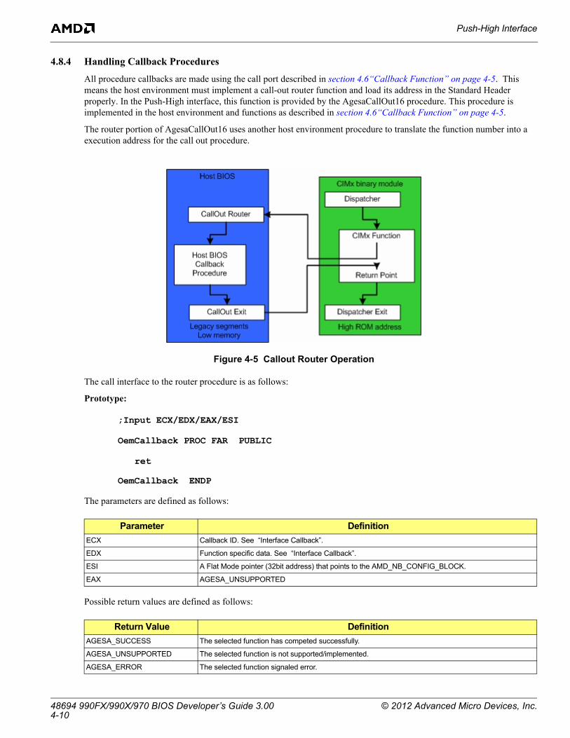
4.8.4 Handling Callback Procedures
All procedure callbacks are made using the call port described in section 4.6“Callback Function” on page 4-5. This means the host environment must implement a call-out router function and load its address in the Standard Header properly. In the Push-High interface, this function is provided by the AgesaCallOut16 procedure. This procedure is implemented in the host environment and functions as described in section 4.6“Callback Function” on page 4-5.
The router portion of AgesaCallOut16 uses another host environment procedure to translate the function number into a execution address for the call out procedure.
Figure 4-5 Callout Router Operation
The call interface to the router procedure is as follows:
Prototype:
;Input ECX/EDX/EAX/ESI
OemCallback PROC FAR PUBLIC
ret
OemCallback ENDP
The parameters are defined as follows:
Possible return values are defined as follows:
Parameter Definition
ECX Callback ID. See “Interface Callback”.
EDX Function specific data. See “Interface Callback”.
ESI A Flat Mode pointer (32bit address) that points to the AMD_NB_CONFIG_BLOCK.
EAX AGESA_UNSUPPORTED
Return Value Definition
AGESA_SUCCESS The selected function has competed successfully.
AGESA_UNSUPPORTED The selected function is not supported/implemented.
AGESA_ERROR The selected function signaled error.
48694 990FX/990X/970 BIOS Developer’s Guide 3.00 © 2012 Advanced Micro Devices, Inc.4-10

Interface Calls
4.8.5 Alternative Callback in 32-Bit Mode
The Push-High interface is designed for use in 16-bit execution legacy BIOS environments; however, any individual callout for a core function may be implemented in 32-bit mode. This permits the author to use the C language and link the function with the CIMx software module, which is loaded in the high area. This reduces the amount of “thunking” and improves execution speed. In addition, it provides the benefits of easier support and reduced maintenance costs. The host environment must modify the build control files to include their customized files.
4.9 Interface Calls
4.9.1 AmdInitializer
Function: Initialize PCIE/HT/NB block configuration structure to default recommended value (refer to CIMx-NB.CHM for details).
Push-High Function ID: PH_Initializer
Prototype:
AGESA_STATUS AmdInitializer(
IN OUT AMD_NB_CONFIG_BLOCK *ConfigPtr
);
The parameter, ConfigPtr, is a pointer to the function’s data structure. Refer to CIMx-NB.CHM (can be CIMx-RD9xx distribution package) for detailed definition of AMD_NB_CONFIG_BLOCK structure.
4.9.2 AmdPowerOnResetInit
Function: Initialize northbridge registers on power-on reset.
Push-High Function ID: PH_amdPowerOnResetInit
Prototype:
AGESA_STATUS AmdPowerOnResetInit(
IN OUT AMD_NB_CONFIG_BLOCK *ConfigPtr
);
The parameter ConfigPtr is a pointer to the function’s data structure. Refer to CIMx-NB.CHM for detailed definition of the AMD_NB_CONFIG_BLOCK structure.
4.9.3 AmdHtInit
Function: Initialize HT subsystem in addition to initialization performed by AGESA.
Push-High Function ID: PH_AmdPowerOnResetInit
Prototype:
AGESA_STATUS AmdHtInit(
IN OUT AMD_NB_CONFIG_BLOCK *ConfigPtr
);
The parameter ConfigPtr is a pointer to the function's data structure. Refer to CIMx-NB.CHM for detailed definition of the AMD_NB_CONFIG_BLOCK structure.
© 2012 Advanced Micro Devices, Inc. 48694 990FX/990X/970 BIOS Developer’s Guide 3.004-11

Interface Calls
4.9.4 AmdPcieEarlyInit
Function: Initialize PCIe subsystem. Train links on all enabled ports. Initialize hot-plug. Result of this calls all PCIe ports in operational state.
Push-High Function ID: PH_amdPcieEarlyInit
Prototype:
AGESA_STATUS AmdPcieEarlyInit (
IN OUT AMD_NB_CONFIG_BLOCK *ConfigPtr
);
The parameter, ConfigPtr, is a pointer to the function’s data structure. Refer to CIMx-NB.CHM for detailed definition of AMD_NB_CONFIG_BLOCK structure.
4.9.5 AmdEarlyPostInit
Function: Initialize miscellaneous northbridge feature at Early Post.
Push-High Function ID: PH_amdEarlyPostInit
Prototype:
AGESA_STATUS AmdEarlyPostInit(
IN OUT AMD_NB_CONFIG_BLOCK *ConfigPtr
);
The parameter, ConfigPtr, is a pointer to the function’s data structure. Refer to CIMx-NB.CHM for detailed definition of the AMD_NB_CONFIG_BLOCK structure.
4.9.6 AmdMidPostInit
Function: Initialize miscellaneous northbridge feature at Mid Post.
Push-High Function Id: PH_amdMidPostInit
Prototype:
AGESA_STATUS AmdMidPostInit (
IN OUT AMD_NB_CONFIG_BLOCK *ConfigPtr
);
The parameter, ConfigPtr, is a pointer to the function’s data structure. Refer to CIMx-NB.CHM for detailed definition of the AMD_NB_CONFIG_BLOCK structure.
The functions AmdEarlyPostInit/AmdMidPostInit/AmdLatePostInit/AmdS3Init must share the same exact copy of the AMD_NB_CONFIG_BLOCK structure.
4.9.7 AmdLatePostInit
Function: Initialize miscellaneous Northbridge feature at Late Post.
Push-High Function Id: PH_amdLatePostInit
Prototype:
AGESA_STATUS AmdLatePostInit(
48694 990FX/990X/970 BIOS Developer’s Guide 3.00 © 2012 Advanced Micro Devices, Inc.4-12

Interface Callback
IN OUT AMD_NB_CONFIG_BLOCK *ConfigPtr
);
The parameter, ConfigPtr, is a pointer to the function’s data structure. Refer to CIMx-NB.CHM for detailed definition of the AMD_NB_CONFIG_BLOCK structure.
The functions AmdEarlyPostInit/AmdMidPostInit/AmdLatePostInit/AmdS3Init must share the same exact copy of the AMD_NB_CONFIG_BLOCK structure.
Note: amdLatePostInit must be run after ACPI tables are created and linked into the RSDT.
4.9.8 AmdS3Init
Function: Initialize PCIe and northbridge feature on S3 resume. See Chapter 6: Power Management for additional details.
Push-High Function Id: PH_amdS3Init
Prototype:
AGESA_STATUS AmdS3Init(
IN OUT AMD_NB_CONFIG_BLOCK *ConfigPtr
);
The parameter, ConfigPtr, is a pointer to the function’s data structure. See CIMx-NB.CHM for detailed definition of the AMD_NB_CONFIG_BLOCK structure.
The functions AmdEarlyPostInit/AmdMidPostInit/AmdLatePostInit/AmdS3Init must share same exact copy of the AMD_NB_CONFIG_BLOCK structure.
4.10 Interface Callback
4.10.1 AmdPortTrainingCompleted
Function: PCIE Port Initialization Completed endpoint detected.
Push-High Callback ID: PHCB_amdPortTrainingCompleted
Prototype:
AGESA_STATUS (*CallOutPtr) (
IN UINT32 CallbackId,IN UINTN PortId,IN OUT AMD_NB_CONFIG_BLOCK *ConfigPtr
);
The parameters are defined as follows:
Return Values:
Parameter Definition
Data PCI Express Port ID.
ConfigPtr Pointer to the function’s data structure. See CIMx-NB.CHM for detailed definition of the AMD_NB_CONFIG_BLOCK structure.
Return Value Definition
AGESA_UNSUPPORTED Callback function not supported.
© 2012 Advanced Micro Devices, Inc. 48694 990FX/990X/970 BIOS Developer’s Guide 3.004-13
Interface Callback
4.10.2 AmdPortResetDeassert
Function: Deassert reset for device connected to PCIe port.
Push-High Callback ID: PHCB_amdPortResetDeassert
Prototype:
AGESA_STATUS (*CallOutPtr) (
IN UINT32 CallbackId,IN UINTN PortIdBitMap,IN OUT AMD_NB_CONFIG_BLOCK *ConfigPtr
);
The parameters are defined as follows:
Return Values:
4.10.3 AmdPortResetAssert
Function: Assert reset for device connected to PCIe port.
Push-High Callback ID: PHCB_amdPortResetAssert
Prototype:
AGESA_STATUS (*CallOutPtr) (
IN UINT32 CallbackId,IN UINTN PortIdBitMap,IN OUT AMD_NB_CONFIG_BLOCK *ConfigPtr
);
The parameters are defined as follows:
Return Values:
AGESA_ERROR Disable port
Parameter Definition
PortIdBitMap Bitmap of port id to deassert reset (0x4 - PortId 2, 0x8 - PortId 3, ...)
ConfigPtr Pointer to the function’s data structure. Refer to CIMx-NB.CHM for detailed definition of AMD_NB_CONFIG_BLOCK structure.
Return Value Definition
AGESA_UNSUPPORTED Callback function not supported.
AGESA_ERROR Disable port
Parameter Definition
PortIdBitMap Bitmap of port id to assert reset (0x4 - PortId 2, 0x8 - PortId 3, ...)
ConfigPtr Pointer to the function’s data structure. Refer to CIMx-NB.CHM for detailed definition of the AMD_NB_CONFIG_BLOCK structure.
Return Value Definition
48694 990FX/990X/970 BIOS Developer’s Guide 3.00 © 2012 Advanced Micro Devices, Inc.4-14
Interface Callback
4.10.4 AmdPortResetSupported
Function: Check if there is controllable reset logic present for device connected to PCIe port.
Push-High Callback ID: PHCB_amdPortResetSupported
Prototype:
AGESA_STATUS (*CallOutPtr) (
IN UINT32 CallbackId,IN UINTN PortId,IN OUT AMD_NB_CONFIG_BLOCK *ConfigPtr
);
The parameters are defined as follows:
Return Values:
4.10.5 AmdAllocateBuffer
Function: Allocate memory buffer
Push-High Callback ID: PHCB_AmdAllocateBuffer
Prototype:
AGESA_STATUS (*CallOutPtr) (
IN UINT32 CallbackId,IN NB_BUFFER_PARAMS *BufferParamPtr,IN OUT AMD_NB_CONFIG_BLOCK *ConfigPtr
);
The parameters are defined as follows:
Return Value Definition
AGESA_UNSUPPORTED Callback function not supported.
AGESA_ERROR Disable port
Parameter Definition
PortId PCIe Port ID.
ConfigPtr Pointer to the function’s data structure. Refer to CIMx-NB.CHM for detailed definition of the AMD_NB_CONFIG_BLOCK structure.
Return Value Definition
AGESA_UNSUPPORTED Callback function not supported
AGESA_SUCCESS Keep port enabled.
AGESA_ERROR Disable PCIe port.
Parameter Definition
BufferParamPtr Pointer to NB_PARAMS_PTR datatype containing length and place holder for address of allocated buffer (see CIMx-NB.CHM for more details).
© 2012 Advanced Micro Devices, Inc. 48694 990FX/990X/970 BIOS Developer’s Guide 3.004-15

Interface Callback
Return Values:
4.10.6 AmdFreeBuffer
Function: De-allocate memory buffer
Usage: Free the memory buffer via PMM function 2 with handle as specified in BufferParamsPtr, and clear the address in BufferParamsPtr on success. ACPI handles will not be explicitly freed, but should be linked into the ACPI table structure after it has been configured by the system BIOS. They may then be freed if necessary.
Push-High Callback ID: PHCB_AmdFreeBuffer
Prototype:
AGESA_STATUS (*CallOutPtr) (
IN UINT32 CallbackId,IN NB_BUFFER_PARAMS *BufferParamPtr,IN OUT AMD_NB_CONFIG_BLOCK *ConfigPtr
);
The parameters are defined as follows:
Return Values:
4.10.7 AmdGeneratePciReset
Function: Generate reset.
Push-High Callback ID: PHCB_amdGeneratePciReset
Prototype:
AGESA_STATUS (*CallOutPtr) (
ConfigPtr Pointer to the function’s data structure. Refer to CIMx-NB.CHM for detailed definition of the AMD_NB_CONFIG_BLOCK structure.
Return Value DefinitionAGESA_UNSUPPORTED Callback function not implemented.
AGESA_SUCCESS Memory allocation succeeded.
AGESA_ERROR Memory allocation failed.
Parameter Definition
BufferParamPtr Pointer to NB_PARAMS_PTR datatype containing handle of buffer to free (see CIMx-NB.CHM for more details).
ConfigPtr Pointer to the function’s data structure. Refer to CIMx-NB.CHM for detailed definition of the AMD_NB_CONFIG_BLOCK structure.
Return Value DefinitionAGESA_UNSUPPORTED Callback function not implemented.
AGESA_SUCCESS Memory allocation succeeded.
AGESA_ERROR Memory allocation failed.
48694 990FX/990X/970 BIOS Developer’s Guide 3.00 © 2012 Advanced Micro Devices, Inc.4-16
Interface Callback
IN UINT32 CallbackId,IN UINTN ResetType,IN OUT AMD_NB_CONFIG_BLOCK *ConfigPtr
);
The parameters are defined as follows:
Return Values:
4.10.8 AmdReportEvent
Function: Report event.
Push-High Callback ID: PHCB_AmdReportEvent
Prototype:
AGESA_STATUS (*CallOutPtr) (
IN UINT32 CallbackId,IN AGESA_EVENT *Event,IN OUT AMD_NB_CONFIG_BLOCK *ConfigPtr
);
The parameters are defined as follows:
Return Values:
4.10.9 AmdUpdateApicInterruptMapping
Function: Update default I/O APIC interrupt mapping.
Push-High Callback ID: PHCB_AmdUpdateApicInterruptMapping
Prototype:
Parameter DefinitionResetType Reser type 0x01 - Warm Reset, 0x02 - Cold Reset
ConfigPtr Pointer to the function’s data structure. Refer to CIMx-NB.CHM for detailed definition of the AMD_NB_CONFIG_BLOCK structure.
Return Value DefinitionAGESA_SUCCESS Debug feature to completely avoid reset generation.
Parameter DefinitionEvent Pinter to event structure
ConfigPtr Pointer to the function’s data structure. Refer to CIMx-NB.CHM for detailed definition of the AMD_NB_CONFIG_BLOCK structure.
Return Value DefinitionAGESA_UNSUPPORTED Callback function not implemented.
AGESA_SUCCESS Event logging succeeded.
AGESA_ERROR Event logging failed
© 2012 Advanced Micro Devices, Inc. 48694 990FX/990X/970 BIOS Developer’s Guide 3.004-17

Interface Callback
AGESA_STATUS (*CallOutPtr) (
IN UINT32 CallbackId,IN APIC_DEVICE_INFO *pApicPortInfo,IN OUT AMD_NB_CONFIG_BLOCK *ConfigPtr
);
The parameters are defined as follows:
Return Values:
4.10.10 AmdPcieAspmInfo
Function: Update PCIe link ASMP info.
Push-High Callback ID: PHCB_AmdPcieAspmInfo
Prototype:
AGESA_STATUS (*CallOutPtr) (
IN UINT32 CallbackId,IN ASPM_LINK_INFO *pAspmLinkInfo,IN OUT AMD_NB_CONFIG_BLOCK *ConfigPtr
);
The parameters are defined as follows:
Return Values:
Parameter DefinitionpApicPortInfo Pointer to array of structutes containing default IO APIC interrupt mapping info. For default interrupt
mapping info (see CIMx-NB.CHM for more details).
ConfigPtr Pointer to the function’s data structure. Refer to CIMx-NB.CHM for detailed definition of the AMD_NB_CONFIG_BLOCK structure.
Return Value DefinitionAGESA_UNSUPPORTED Callback function not implemented (default interrupt mapping will be used).
AGESA_SUCCESS Interrupt table updated.
Parameter Definition
pAspmLinkInfo Pointer to structure containing ASPM link information (see CIMx-NB.CHM for more details).
ConfigPtr Pointer to the function’s data structure. Refer to CIMx-NB.CHM for detailed definition of the AMD_NB_CONFIG_BLOCK structure.
Return Value Definition
AGESA_UNSUPPORTED Callback function not implemented (default interrupt mapping will be used).
AGESA_SUCCESS Link ASPM info updated.
48694 990FX/990X/970 BIOS Developer’s Guide 3.00 © 2012 Advanced Micro Devices, Inc.4-18

Architectural Details of IOMMU
4.11 Architectural Details of IOMMU
4.11.1 Theory of Operation
The IOMMU is a system function that translates addresses used in DMA transactions, protects memory from illegal access by I/O devices, and remaps peripheral interrupts. A single northbridge will typically include one IOMMU device for all the components of that device. Unlike many PCI devices, the base address may be written only once, and is located in the IOMMU capability block.
There are three logical components to configuring an IOMMU. First, each IOMMU will be initialized and granted a base address. Second, all IOMMU devices will be described in an ACPI table. Third, the ACPI table will be patched with the APIC IDs, found from the ACPI MADT table, for each northbridge.
4.11.2 Requirements
In order to enable the IOMMU two pieces of data are necessary:
IommuBaseAddress – a 16KB aligned memory 64-bit memory address where the IOMMU will be located in memory. It must be provided in each northbridge configuration block, as each IOMMU in a multi-northbridge configuration will require resources to be assigned. If a value of NULL or 0 is provided, the IOMMU corresponding to that northbridge block will be disabled (see CIMX-NB.CHM for more details on the northbridge configuration structure)
AmdAllocateBuffer is a callback made to the host BIOS in order to reserve a memory buffer where the IVRS is to be created. A single IVRS table will be created for all IOMMU devices found in a system (see CIMX-NB.CHM for more details).
4.11.3 Execution
Enabling the IOMMU is done as a three step process in AmdMidPost and AmdLatePost. An IVRS table will be returned, which must be added to the ACPI table hierarchy. The final patch phase must be run after the ACPI MADT and ACPI IVRS tables are linked to the RSDT.
IOMMU Initialization (AmdMidPostInit) – Each northbridge is checked for a compatible IOMMU type, subsystem ID is programmed to match the northbridge, and initial settings are made.
ACPI IVRS Initialization (AmdMidPostInit) – The IVRS (I/O Virtualization Structure) is generated for the system, and each IOMMU is given an IVHD sub-entry. The peripheral device hierarchy respective to each IOMMU is programmed as well.
ACPI IVRS Patching (AmdLatePostInit) – Each IVRS special device (type 72) entry for AMD devices is patched with an instance handle. In the case of the IOAPIC entry, the APIC ID is patched by correlating the ACPI MADT IOAPIC base address entry to the AMD northbridge or southbridge device, and programming this APIC identifier into the handle field in the type 72 entry.
4.12 Legacy Wrapper Example
See Legacy wrapper example implementation located at \Addendum\RD9xx\Wrapper in CIMx package.
© 2012 Advanced Micro Devices, Inc. 48694 990FX/990X/970 BIOS Developer’s Guide 3.004-19

Legacy Wrapper Example
This page is left blank intentionally.
48694 990FX/990X/970 BIOS Developer’s Guide 3.00 © 2012 Advanced Micro Devices, Inc.4-20

Chapter 5UEFI Support
5.1 UEFI Driver Information
For UEFI driver information see CIMx-NB.CHM file.
© 2012 Advanced Micro Devices, Inc. 48694 990FX/990X/970 BIOS Developer’s Guide 3.005-1

UEFI Driver Information
This page is left blank intentionally.
48694 990FX/990X/970 BIOS Developer’s Guide 3.00 © 2012 Advanced Micro Devices, Inc.5-2

Chapter 6Power Management
6.1 Sx State Power Management
During certain Sx states (such as S1) the system maintains power to the RD9xx and all register settings are retained. Therefore, no action is required when the system resumes. However, under other S states (such as S3), typical designs will shut down power to the RD9xx and all of the register settings will be lost.
The SBIOS is responsible for reinitializing all of the RD9xx registers. Reinitializing the RD9xx registers after S3 can be done by either restoring the tables of register settings which were saved to non-volatile storage prior to entering S3, or by initializing all registers as if from cold.
For most configurations restoration by table is not practical. The recommendation is to re-execute the initialization code.
The remaining NB registers are covered in section 6.1.1.
6.1.1 Register Restoration
The registers listed in this section are restored after the system memory is made available by bringing the system RAM out of self refresh mode.
On RD9xx designs, the main system memory is controlled by the memory controller in the AMD CPU. (For more information on saving and restoring the memory controller settings, along with entering and exiting self refresh mode, refer to the “AMD Kernel BIOS writers guide”.) The reference BIOS saves the registers listed in this section prior to entering S3. It then restores them after system memory is available on resume from S3.
Note: The list of registers in the following sections is subject to change. If an OEM customer changes any other registers in the RD9xx during POST, then they must also be restored on an S3 resume.
• Northbridge (0:0:0)
• 0x04 - 0x06
• 0x4C - 0x4F
• 0x8C - 0x8F
• PCIe Bridges (0:2/3/4/5/7/9/10/11/12/13:0)
• 0x18 - 0x1B
• 0x20 - 0x23
• 0x24 - 0x27
• 0x2C - 0x2F
• 0x04 - 0x06
6.1.2 Resume from S3 State
When the system wakes up from S3 the BIOS is initially executed from ROM, once it is determined this is an S3 resume. The SBIOS is responsible for restoring the system memory controller’s configuration as outlined in the “AMD Kernel BIOS Writer’s Guide”.
Once the system memory is available the BIOS should then restore the RD9xx registers that were saved prior to entering S3.
© 2012 Advanced Micro Devices, Inc. 48694 990FX/990X/970 BIOS Developer’s Guide 3.006-1

Sx State Power Management
This page is left blank intentionally.
48694 990FX/990X/970 BIOS Developer’s Guide 3.00 © 2012 Advanced Micro Devices, Inc.6-2