Embed Size (px)
Citation preview

VOUTP
VOUTN
VDD2
GND2GND1
VINP
VINN
VDD1
AMC1301-Q1
HV+
HV-
To Load
FloatingPower Supply
3.3 V or 5.0 V
RSHUNT
Gate Driver
Gate Driver
ADC121S101-Q1 12-Bit ADC
3.3 V or 5.0 V
Rei
nfor
ced
Isol
atio
n
Copyright © 2016, Texas Instruments Incorporated
Product
Folder
Order
Now
Technical
Documents
Tools &
Software
Support &Community
ReferenceDesign
An IMPORTANT NOTICE at the end of this data sheet addresses availability, warranty, changes, use in safety-critical applications,intellectual property matters and other important disclaimers. PRODUCTION DATA.
AMC1301-Q1SBAS792A –APRIL 2017–REVISED APRIL 2017
AMC1301-Q1 Precision, ±250-mV Input, 3-µs Delay, Reinforced Isolated Amplifier
1
1 Features1• Qualified for Automotive Applications• AEC-Q100 Qualified with the Following Results:
– Temperature Grade 1: –40°C to 125°C– HBM ESD Classification Level 2– CDM ESD Classification Level C6
• Low Offset Error and Drift:±200 µV at 25°C, ± 3 µV/°C
• Fixed Gain: 8.2• Very Low Gain Error and Drift:
±0.3% at 25°C, ± 50 ppm/°C• Very Low Nonlinearity and Drift:
0.03%, 1 ppm/°C• 3.3-V Operation on High-Side and Low-Side• System-Level Diagnostic Features• Safety-Related Certifications:
– 7000-VPK Reinforced Isolation perDIN V VDE V 0884-10 (VDE V 0884-10):2006-12
– 5000-VRMS Isolation for 1 Minute per UL1577– CAN/CSA No. 5A-Component Acceptance
Service Notice
2 Applications• Shunt-Based Current Sensing or Resistor-Divider-
Based Voltage Sensing In:– Traction Inverters– Onboard Chargers (OBC)– DC-DC Converters– Battery Management Systems (BMS)
3 DescriptionThe AMC1301-Q1 device is a precision, isolatedamplifier with an output separated from the inputcircuitry by an isolation barrier that is highly resistantto magnetic interference. This barrier is certified toprovide reinforced galvanic isolation of up to 7 kVPEAKaccording to VDE V 0884-10 and UL1577. Used inconjunction with isolated power supplies, this deviceprevents noise currents on a high common-modevoltage line from entering the local ground andinterfering with or damaging sensitive circuitry.
The input of the AMC1301-Q1 device is optimized fordirect connection to shunt resistors or other lowvoltage-level signal sources. The excellentperformance of the device supports accurate currentcontrol resulting in system-level power savings and,especially in motor control applications, lower torqueripple. The integrated common-mode overvoltage andmissing high-side supply voltage detection features ofthe AMC1301-Q1 device simplify system-level designand diagnostics.
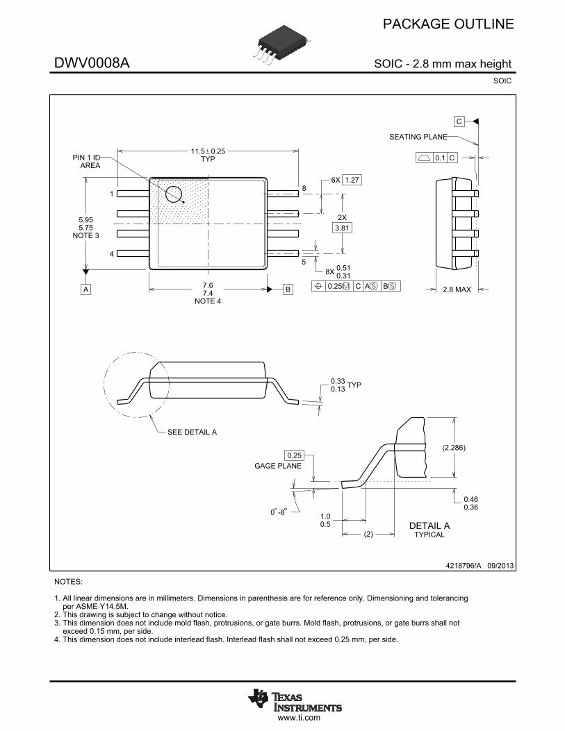
The AMC1301-Q1 device is available in a wide-body8-pin SOIC (DWV) package.
Device Information(1)
PART NUMBER PACKAGE BODY SIZE (NOM)AMC1301-Q1 SOIC (8) 5.85 mm × 7.50 mm
(1) For all available packages, see the orderable addendum atthe end of the data sheet.
Simplified Schematic

2
AMC1301-Q1SBAS792A –APRIL 2017–REVISED APRIL 2017 www.ti.com
Product Folder Links: AMC1301-Q1
Submit Documentation Feedback Copyright © 2017, Texas Instruments Incorporated
Table of Contents1 Features .................................................................. 12 Applications ........................................................... 13 Description ............................................................. 14 Revision History..................................................... 25 Pin Configuration and Functions ......................... 36 Specifications......................................................... 4
6.1 Absolute Maximum Ratings ...................................... 46.2 ESD Ratings.............................................................. 46.3 Recommended Operating Conditions....................... 46.4 Thermal Information .................................................. 46.5 Power Ratings........................................................... 46.6 Insulation Specifications............................................ 56.7 Safety-Related Certifications..................................... 66.8 Safety Limiting Values .............................................. 66.9 Electrical Characteristics........................................... 66.10 Insulation Characteristics Curves .......................... 86.11 Typical Characteristics ............................................ 9
7 Parameter Measurement Information ................ 167.1 Timing Diagrams..................................................... 16
8 Detailed Description ............................................ 17
8.1 Overview ................................................................. 178.2 Functional Block Diagram ....................................... 178.3 Feature Description................................................. 178.4 Device Functional Modes........................................ 18
9 Application and Implementation ........................ 199.1 Application Information............................................ 199.2 Typical Applications ................................................ 199.3 Do's and Don'ts ...................................................... 23
10 Power Supply Recommendations ..................... 2411 Layout................................................................... 25
11.1 Layout Guidelines ................................................. 2511.2 Layout Example .................................................... 25
12 Device and Documentation Support ................. 2612.1 Documentation Support ....................................... 2612.2 Receiving Notification of Documentation Updates 2612.3 Community Resources.......................................... 2612.4 Trademarks ........................................................... 2612.5 Electrostatic Discharge Caution............................ 2612.6 Glossary ................................................................ 26
13 Mechanical, Packaging, and OrderableInformation ........................................................... 26
4 Revision HistoryNOTE: Page numbers for previous revisions may differ from page numbers in the current version.
Changes from Original (April 2017) to Revision A Page
• Changed maximum specification of Supply voltage row in Absolute Maximum Ratings table from 6.5 V to 7 V ................. 4

Not to scale
1VDD1 8 VDD2
2VINP 7 VOUTP
3VINN 6 VOUTN
4GND1 5 GND2
3
AMC1301-Q1www.ti.com SBAS792A –APRIL 2017–REVISED APRIL 2017
Product Folder Links: AMC1301-Q1
Submit Documentation FeedbackCopyright © 2017, Texas Instruments Incorporated
5 Pin Configuration and Functions
DWV Package8-Pin SOICTop View
Pin FunctionsPIN
I/O DESCRIPTIONNAME NO.
GND1 4 — High-side analog groundGND2 5 — Low-side analog ground
VDD1 1 — High-side power supply, 3.0 V to 5.5 V.See the Power Supply Recommendations section for decoupling recommendations.
VDD2 8 — Low-side power supply, 3.0 V to 5.5 V.See the Power Supply Recommendations section for decoupling recommendations.
VINN 3 I Inverting analog inputVINP 2 I Noninverting analog inputVOUTN 6 O Inverting analog outputVOUTP 7 O Noninverting analog output
4
AMC1301-Q1SBAS792A –APRIL 2017–REVISED APRIL 2017 www.ti.com
Product Folder Links: AMC1301-Q1
Submit Documentation Feedback Copyright © 2017, Texas Instruments Incorporated
(1) Stresses beyond those listed under Absolute Maximum Ratings may cause permanent damage to the device. These are stress ratingsonly, which do not imply functional operation of the device at these or any other conditions beyond those indicated under RecommendedOperating Conditions. Exposure to absolute-maximum-rated conditions for extended periods may affect device reliability.
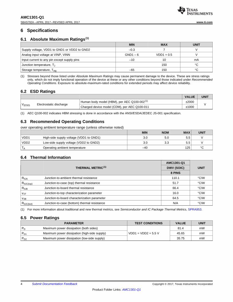
6 Specifications
6.1 Absolute Maximum Ratings (1)
MIN MAX UNITSupply voltage, VDD1 to GND1 or VDD2 to GND2 –0.3 7 VAnalog input voltage at VINP, VINN GND1 – 6 VDD1 + 0.5 VInput current to any pin except supply pins –10 10 mAJunction temperature, TJ 150 °CStorage temperature, Tstg –65 150 °C
(1) AEC Q100-002 indicates HBM stressing is done in accordance with the ANSI/ESDA/JEDEC JS-001 specification.
6.2 ESD RatingsVALUE UNIT
V(ESD) Electrostatic dischargeHuman body model (HBM), per AEC Q100-002 (1) ±2000
VCharged device model (CDM), per AEC Q100-011 ±1000
6.3 Recommended Operating Conditionsover operating ambient temperature range (unless otherwise noted)
MIN NOM MAX UNITVDD1 High-side supply voltage (VDD1 to GND1) 3.0 5.0 5.5 VVDD2 Low-side supply voltage (VDD2 to GND2) 3.0 3.3 5.5 VTA Operating ambient temperature –40 125 °C
(1) For more information about traditional and new thermal metrics, see Semiconductor and IC Package Thermal Metrics, SPRA953.
6.4 Thermal Information
THERMAL METRIC (1)AMC1301-Q1
UNITDWV (SOIC)8 PINS
RθJA Junction-to-ambient thermal resistance 110.1 °C/WRθJC(top) Junction-to-case (top) thermal resistance 51.7 °C/WRθJB Junction-to-board thermal resistance 66.4 °C/WψJT Junction-to-top characterization parameter 16.0 °C/WψJB Junction-to-board characterization parameter 64.5 °C/WRθJC(bot) Junction-to-case (bottom) thermal resistance N/A °C/W
6.5 Power RatingsPARAMETER TEST CONDITIONS VALUE UNIT
PD Maximum power dissipation (both sides)VDD1 = VDD2 = 5.5 V
81.4 mWPD1 Maximum power dissipation (high-side supply) 45.65 mWPD2 Maximum power dissipation (low-side supply) 35.75 mW
5
AMC1301-Q1www.ti.com SBAS792A –APRIL 2017–REVISED APRIL 2017
Product Folder Links: AMC1301-Q1
Submit Documentation FeedbackCopyright © 2017, Texas Instruments Incorporated
(1) Apply creepage and clearance requirements according to the specific equipment isolation standards of an application. Care must betaken to maintain the creepage and clearance distance of a board design to ensure that the mounting pads of the isolator on the printedcircuit board (PCB) do not reduce this distance. Creepage and clearance on a PCB become equal in certain cases. Techniques such asinserting grooves and ribs on the PCB are used to help increase these specifications.
(2) This coupler is suitable for safe electrical insulation only within the safety ratings. Compliance with the safety ratings shall be ensured bymeans of suitable protective circuits.
(3) Testing is carried out in air or oil to determine the intrinsic surge immunity of the isolation barrier.(4) Apparent charge is electrical discharge caused by a partial discharge (pd).(5) All pins on each side of the barrier are tied together, creating a two-pin device.
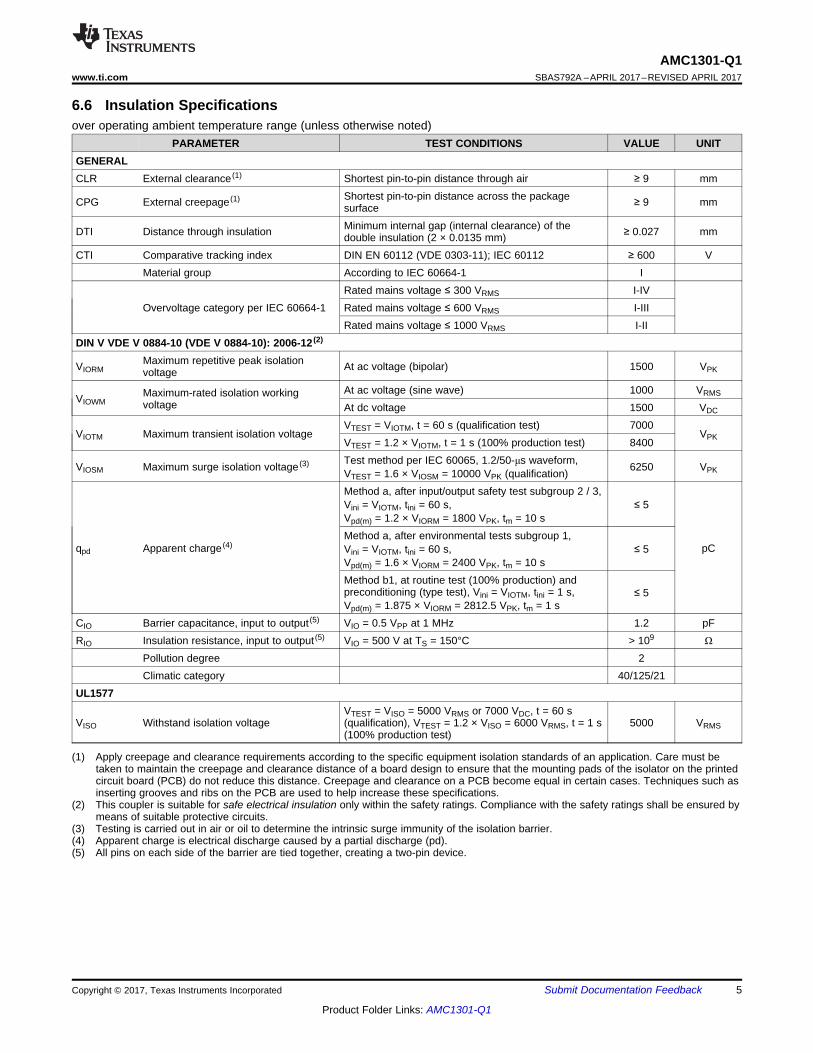
6.6 Insulation Specificationsover operating ambient temperature range (unless otherwise noted)
PARAMETER TEST CONDITIONS VALUE UNITGENERALCLR External clearance (1) Shortest pin-to-pin distance through air ≥ 9 mm
CPG External creepage (1) Shortest pin-to-pin distance across the packagesurface ≥ 9 mm
DTI Distance through insulation Minimum internal gap (internal clearance) of thedouble insulation (2 × 0.0135 mm) ≥ 0.027 mm
CTI Comparative tracking index DIN EN 60112 (VDE 0303-11); IEC 60112 ≥ 600 VMaterial group According to IEC 60664-1 I
Overvoltage category per IEC 60664-1Rated mains voltage ≤ 300 VRMS I-IVRated mains voltage ≤ 600 VRMS I-IIIRated mains voltage ≤ 1000 VRMS I-II
DIN V VDE V 0884-10 (VDE V 0884-10): 2006-12 (2)
VIORMMaximum repetitive peak isolationvoltage At ac voltage (bipolar) 1500 VPK
VIOWMMaximum-rated isolation workingvoltage
At ac voltage (sine wave) 1000 VRMS
At dc voltage 1500 VDC
VIOTM Maximum transient isolation voltageVTEST = VIOTM, t = 60 s (qualification test) 7000
VPKVTEST = 1.2 × VIOTM, t = 1 s (100% production test) 8400
VIOSM Maximum surge isolation voltage (3) Test method per IEC 60065, 1.2/50-μs waveform,VTEST = 1.6 × VIOSM = 10000 VPK (qualification) 6250 VPK
qpd Apparent charge (4)
Method a, after input/output safety test subgroup 2 / 3,Vini = VIOTM, tini = 60 s,Vpd(m) = 1.2 × VIORM = 1800 VPK, tm = 10 s
≤ 5
pCMethod a, after environmental tests subgroup 1,Vini = VIOTM, tini = 60 s,Vpd(m) = 1.6 × VIORM = 2400 VPK, tm = 10 s
≤ 5
Method b1, at routine test (100% production) andpreconditioning (type test), Vini = VIOTM, tini = 1 s,Vpd(m) = 1.875 × VIORM = 2812.5 VPK, tm = 1 s
≤ 5
CIO Barrier capacitance, input to output (5) VIO = 0.5 VPP at 1 MHz 1.2 pFRIO Insulation resistance, input to output (5) VIO = 500 V at TS = 150°C > 109 Ω
Pollution degree 2Climatic category 40/125/21
UL1577
VISO Withstand isolation voltageVTEST = VISO = 5000 VRMS or 7000 VDC, t = 60 s(qualification), VTEST = 1.2 × VISO = 6000 VRMS, t = 1 s(100% production test)
5000 VRMS

6
AMC1301-Q1SBAS792A –APRIL 2017–REVISED APRIL 2017 www.ti.com
Product Folder Links: AMC1301-Q1
Submit Documentation Feedback Copyright © 2017, Texas Instruments Incorporated
6.7 Safety-Related CertificationsVDE UL
Certified according to DIN V VDE V 0884-10 (VDE V 0884-10):2006-12, DIN EN 60950-1 (VDE 0805 Teil 1): 2014-08, and
DIN EN 60065 (VDE 0860): 2005-11
Recognized under 1577 component recognition andCSA component acceptance NO 5 programs
Reinforced insulation Single protectionCertificate number: 40040142 File number: E181974
(1) Input, output, or the sum of input and output power must not exceed this value.
6.8 Safety Limiting ValuesSafety limiting intends to prevent potential damage to the isolation barrier upon failure of input or output (I/O) circuitry.A failure of the I/O may allow low resistance to ground or the supply and, without current limiting, dissipate sufficient power tooverheat the die and damage the isolation barrier, potentially leading to secondary system failures.
PARAMETER TEST CONDITIONS MIN TYP MAX UNIT
ISSafety input, output, or supplycurrent
θJA = 110.1°C/W, VI = 5.5 V, TJ = 150°C,TA = 25°C 206
mAθJA = 110.1°C/W, VI = 3.6 V, TJ = 150°C,TA = 25°C 315
PS Safety input, output, or total power θJA = 110.1°C/W, TJ = 150°C, TA = 25°C 1135 (1) mWTS Maximum safety temperature 150 °C
(1) Steady-state voltage supported by the device in case of a system failure. See specified common-mode input voltage VCM for normaloperation. Observe analog input voltage range as specified in Absolute Maximum Ratings.
The maximum safety temperature is the maximum junction temperature specified for the device. The powerdissipation and junction-to-air thermal impedance of the device installed in the application hardware determinesthe junction temperature. The assumed junction-to-air thermal resistance in the Thermal Information table is thatof a device installed on a high-K test board for leaded surface-mount packages. The power is the recommendedmaximum input voltage times the current. The junction temperature is then the ambient temperature plus thepower times the junction-to-air thermal resistance.
6.9 Electrical CharacteristicsMinimum and maximum specifications apply from TA = –40°C to +125°C, VDD1 = 3.0 V to 5.5 V, VDD2 = 3.0 V to 5.5 V,VINP = –250 mV to +250 mV, and VINN = 0 V. Typical specifications are at TA = 25°C, VDD1 = 5 V, and VDD2 = 3.3 V(unless otherwise noted).
PARAMETER TEST CONDITIONS MIN TYP MAX UNITANALOG INPUT
VClippingDifferential input voltage before clippingoutput VINP – VINN ±302.7 mV
VFSR Specified linear differential full-scale VINP – VINN –250 250 mVVCM Specified common-mode input voltage (VINP + VINN) / 2 to GND1 –0.16 VDD1 – 2.1 V
Absolute common-mode input voltage (1) (VINN + VINP) / 2 to GND1 –2 VDD1 V
VCMovCommon-mode overvoltage detectionlevel VDD1 – 2 V
VOS Input offset voltage Initial, at TA = 25°C, VINP = VINN = GND1 –200 ±50 200 µVTCVOS Input offset drift –3 ±1 3 µV/°C
CMRR Common-mode rejection ratiofIN = 0 Hz, VCM min ≤ VCM ≤ VCM max –93
dBfIN = 10 kHz, VCM min ≤ VCM ≤ VCM max –93
CIND Differential input capacitance 1 pFRIN Single-ended input resistance VINN = GND1 18 kΩRIND Differential input resistance 22 kΩIIB Input bias current VINP = VINN = GND1 –82 –60 –48 µATCIIB Input bias current drift 1 nA/°CBWIN Input bandwidth 1000 kHz

7
AMC1301-Q1www.ti.com SBAS792A –APRIL 2017–REVISED APRIL 2017
Product Folder Links: AMC1301-Q1
Submit Documentation FeedbackCopyright © 2017, Texas Instruments Incorporated
Electrical Characteristics (continued)Minimum and maximum specifications apply from TA = –40°C to +125°C, VDD1 = 3.0 V to 5.5 V, VDD2 = 3.0 V to 5.5 V,VINP = –250 mV to +250 mV, and VINN = 0 V. Typical specifications are at TA = 25°C, VDD1 = 5 V, and VDD2 = 3.3 V(unless otherwise noted).
PARAMETER TEST CONDITIONS MIN TYP MAX UNITANALOG OUTPUT
Nominal gain 8.2EG Gain error Initial, at TA = 25°C –0.3% ±0.05% 0.3%TCEG Gain error drift –50 ±15 50 ppm/°C
Nonlinearity –0.03% ±0.01% 0.03%Nonlinearity drift 1 ppm/°C
THD Total harmonic distortion fIN = 10 kHz –87 dB
Output noise VINP = VINN = GND1, fIN = 0 Hz,BW = 100 kHz 220 μVRMS
SNR Signal-to-noise ratiofIN = 1 kHz, BW = 10 kHz 80 84
dBfIN = 10 kHz, BW = 100 kHz 71
PSRR Power-supply rejection ratio
vs VDD1, at dc –94
dBvs VDD1, 100-mV and 10-kHz ripple –90vs VDD2, at dc –100vs VDD2, 100-mV and 10-kHz ripple –94
tr Rise time See Figure 45 2.0 µstf Fall time See Figure 45 2.0 µs
VIN to VOUT signal delay (50% – 10%) See Figure 46, unfiltered output 0.7 2.0 µsVIN to VOUT signal delay (50% – 50%) See Figure 46, unfiltered output 1.6 2.6 µsVIN to VOUT signal delay (50% – 90%) See Figure 46, unfiltered output 2.5 3.0 µs
CMTI Common-mode transient immunity |GND1 – GND2| = 1 kV 15 kV/µsVCMout Common-mode output voltage 1.39 1.44 1.49 V
Output short-circuit current ±13 mAROUT Output resistance on VOUTP or VOUTN < 0.2 Ω
BW Output bandwidth 190 210 kHzVFAILSAFE Failsafe differential output voltage VCM ≥ VCMov, or VDD1 missing –2.563 –2.545 VPOWER SUPPLY
IDD1 High-side supply current3.0 V ≤ VDD1 ≤ 3.6 V 5.0 6.9
mA4.5 V ≤ VDD1 ≤ 5.5 V 5.9 8.3
IDD2 Low-side supply current3.0 V ≤ VDD2 ≤ 3.6 V 4.4 5.6
mA4.5 V ≤ VDD2 ≤ 5.5 V 4.8 6.5
PDD1 High-side power dissipation3.0 V ≤ VDD1 ≤ 3.6 V 16.5 24.84
mW4.5 V ≤ VDD1 ≤ 5.5 V 29.5 45.65
PDD2 Low-side power dissipation3.0 V ≤ VDD2 ≤ 3.6 V 14.52 20.16
mW4.5 V ≤ VDD2 ≤ 5.5 V 24 35.75
TA (°C)
I S (
mA
)
0 50 100 150 2000
100
200
300
400
500
D043
VDD1 = VDD2 = 3.6 VVDD1 = VDD2 = 5.5 V
TA (°C)
PS (
mW
)
0 50 100 150 2000
100
200
300
400
500
600
700
800
900
1000
1100
1200
1300
D044
8
AMC1301-Q1SBAS792A –APRIL 2017–REVISED APRIL 2017 www.ti.com
Product Folder Links: AMC1301-Q1
Submit Documentation Feedback Copyright © 2017, Texas Instruments Incorporated
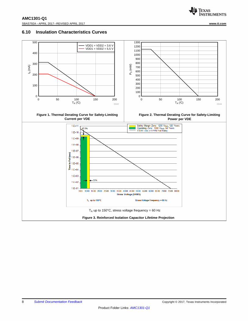
6.10 Insulation Characteristics Curves
Figure 1. Thermal Derating Curve for Safety-LimitingCurrent per VDE
Figure 2. Thermal Derating Curve for Safety-LimitingPower per VDE
TA up to 150°C, stress voltage frequency = 60 Hz
Figure 3. Reinforced Isolation Capacitor Lifetime Projection

VDDx (V)
VO
S (P
V)
3 3.25 3.5 3.75 4 4.25 4.5 4.75 5 5.25 5.5-200
-150
-100
-50
0
50
100
150
200
D005
vs VDD1vs VDD2
Temperature (°C)
VO
S (P
V)
-40 -25 -10 5 20 35 50 65 80 95 110 125-200
-150
-100
-50
0
50
100
150
200
D006
Device 1Device 2Device 3
VOS (PV)
Dev
ices
(%
)
0
10
20
30
40
50
-200
-175
-150
-125
-100 -75
-50
-25 0 25 50 75 100
125
150
175
200
D003 VOS (PV)
Dev
ices
(%
)
0
10
20
30
40
50
-200
-175
-150
-125
-100 -75
-50
-25 0 25 50 75 100
125
150
175
200
D004
VDD1 (V)
VC
Mov
(V
)
3 3.25 3.5 3.75 4 4.25 4.5 4.75 5 5.25 5.51
1.4
1.8
2.2
2.6
3
3.4
3.8
D001Temperature (°C)
VC
Mov
(V
)
-40 -25 -10 5 20 35 50 65 80 95 110 1251
1.4
1.8
2.2
2.6
3
3.4
3.8
D002
9
AMC1301-Q1www.ti.com SBAS792A –APRIL 2017–REVISED APRIL 2017
Product Folder Links: AMC1301-Q1
Submit Documentation FeedbackCopyright © 2017, Texas Instruments Incorporated
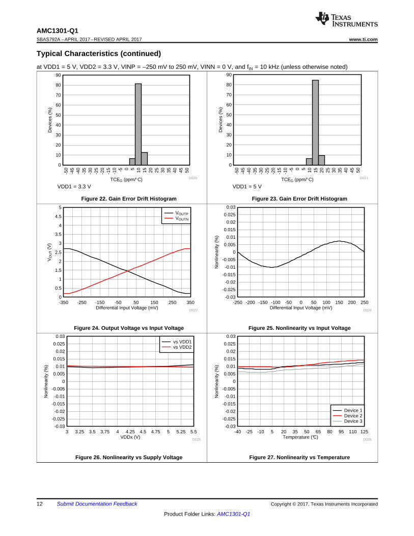
6.11 Typical Characteristicsat VDD1 = 5 V, VDD2 = 3.3 V, VINP = –250 mV to 250 mV, VINN = 0 V, and fIN = 10 kHz (unless otherwise noted)
Figure 4. Common-Mode Overvoltage Detection Levelvs High-Side Supply Voltage
Figure 5. Common-Mode Overvoltage Detection Levelvs Temperature
VDD1 = 3.3 V
Figure 6. Input Offset Voltage Histogram
VDD1 = 5 V
Figure 7. Input Offset Voltage Histogram
Figure 8. Input Offset Voltage vs Supply Voltage Figure 9. Input Offset Voltage vs Temperature

VCM (V)
I IB (P
A)
-0.5 0 0.5 1 1.5 2 2.5 3-80
-60
-40
-20
0
20
40
60
D012VDD1 (V)
I IB (P
A)
3 3.25 3.5 3.75 4 4.25 4.5 4.75 5 5.25 5.5-82
-78
-74
-70
-66
-62
-58
-54
-50
-46
D013
fIN (kHz)
CM
RR
(dB
)
0.001 0.01 0.1 0.5 2 3 5 10 20 100 1000-120
-100
-80
-60
-40
-20
0
D009Temperature (°C)
CM
RR
(dB
)
-40 -25 -10 5 20 35 50 65 80 95 110 125-110
-105
-100
-95
-90
-85
-80
-75
-70
-65
-60
D011
TCVOS (PV/qC)
Dev
ices
(%
)
0
10
20
30
40
50
60
70
-3
-2.5 -2
-1.5 -1
-0.5 0
0.5 1
1.5 2
2.5 3
D007 TCVOS (PV/qC)
Dev
ices
(%
)
0
10
20
30
40
50
60
70
-3
-2.5 -2
-1.5 -1
-0.5 0
0.5 1
1.5 2
2.5 3
D008
10
AMC1301-Q1SBAS792A –APRIL 2017–REVISED APRIL 2017 www.ti.com
Product Folder Links: AMC1301-Q1
Submit Documentation Feedback Copyright © 2017, Texas Instruments Incorporated
Typical Characteristics (continued)at VDD1 = 5 V, VDD2 = 3.3 V, VINP = –250 mV to 250 mV, VINN = 0 V, and fIN = 10 kHz (unless otherwise noted)
VDD1 = 3.3 V
Figure 10. Input Offset Drift Histogram
VDD1 = 5 V
Figure 11. Input Offset Drift Histogram
Figure 12. Common-Mode Rejection Ratiovs Input Frequency
Figure 13. Common-Mode Rejection Ratiovs Temperature
Figure 14. Input Bias Currentvs Common-Mode Input Voltage
Figure 15. Input Bias Currentvs High-Side Supply Voltage

VDDx (V)
EG
(%
)
3 3.25 3.5 3.75 4 4.25 4.5 4.75 5 5.25 5.5-0.3
-0.25
-0.2
-0.15
-0.1
-0.05
0
0.05
0.1
0.15
0.2
0.25
0.3
D018
vs VDD1vs VDD2
Temperature (°C)
EG
(%
)
-40 -25 -10 5 20 35 50 65 80 95 110 125-0.3
-0.25
-0.2
-0.15
-0.1
-0.05
0
0.05
0.1
0.15
0.2
0.25
0.3
D019
Device 1Device 2Device 3
EG (%)
Dev
ices
(%
)
0
10
20
30
40
50
-0.3
-0.2
5
-0.2
-0.1
5
-0.1
-0.0
5 0
0.05 0.1
0.15 0.2
0.25 0.3
D016 EG (%)
Dev
ices
(%
)
0
10
20
30
40
50
-0.3
-0.2
5
-0.2
-0.1
5
-0.1
-0.0
5 0
0.05 0.1
0.15 0.2
0.25 0.3
D017
Temperature (°C)
I IB (P
A)
-40 -25 -10 5 20 35 50 65 80 95 110 125-82
-78
-74
-70
-66
-62
-58
-54
-50
-46
D014Input Signal Frequency (kHz)
Nor
mal
ized
Gai
n (d
B)
0.01 0.1 1 10 100 1000-80
-70
-60
-50
-40
-30
-20
-10
0
D015
11
AMC1301-Q1www.ti.com SBAS792A –APRIL 2017–REVISED APRIL 2017
Product Folder Links: AMC1301-Q1
Submit Documentation FeedbackCopyright © 2017, Texas Instruments Incorporated
Typical Characteristics (continued)at VDD1 = 5 V, VDD2 = 3.3 V, VINP = –250 mV to 250 mV, VINN = 0 V, and fIN = 10 kHz (unless otherwise noted)
Figure 16. Input Bias Current vs Temperature Figure 17. Normalized Gain vs Input Frequency
VDD1 = 3.3 V
Figure 18. Gain Error Histogram
VDD1 = 5 V
Figure 19. Gain Error Histogram
Figure 20. Gain Error vs Supply Voltage Figure 21. Gain Error vs Temperature
VDDx (V)
Non
linea
rity
(%)
3 3.25 3.5 3.75 4 4.25 4.5 4.75 5 5.25 5.5-0.03
-0.025
-0.02
-0.015
-0.01
-0.005
0
0.005
0.01
0.015
0.02
0.025
0.03
D025
vs VDD1vs VDD2
Temperature (°C)
Non
linea
rity
(%)
-40 -25 -10 5 20 35 50 65 80 95 110 125-0.03
-0.025
-0.02
-0.015
-0.01
-0.005
0
0.005
0.01
0.015
0.02
0.025
0.03
D026
Device 1Device 2Device 3
Differential Input Voltage (mV)
VO
UT (
V)
-350 -250 -150 -50 50 150 250 3500
0.5
1
1.5
2
2.5
3
3.5
4
4.5
5
D022
VOUTPVOUTN
Differential Input Voltage (mV)
Non
linea
rity
(%)
-250 -200 -150 -100 -50 0 50 100 150 200 250-0.03
-0.025
-0.02
-0.015
-0.01
-0.005
0
0.005
0.01
0.015
0.02
0.025
0.03
D024
TCEG (ppm/qC)
Dev
ices
(%
)
0
10
20
30
40
50
60
70
80
90
-50
-45
-40
-35
-30
-25
-20
-15
-10 -5 0 5 10 15 20 25 30 35 40 45 50
D020 TCEG (ppm/qC)
Dev
ices
(%
)
0
10
20
30
40
50
60
70
80
90
-50
-45
-40
-35
-30
-25
-20
-15
-10 -5 0 5 10 15 20 25 30 35 40 45 50
D021
12
AMC1301-Q1SBAS792A –APRIL 2017–REVISED APRIL 2017 www.ti.com
Product Folder Links: AMC1301-Q1
Submit Documentation Feedback Copyright © 2017, Texas Instruments Incorporated
Typical Characteristics (continued)at VDD1 = 5 V, VDD2 = 3.3 V, VINP = –250 mV to 250 mV, VINN = 0 V, and fIN = 10 kHz (unless otherwise noted)
VDD1 = 3.3 V
Figure 22. Gain Error Drift Histogram
VDD1 = 5 V
Figure 23. Gain Error Drift Histogram
Figure 24. Output Voltage vs Input Voltage Figure 25. Nonlinearity vs Input Voltage
Figure 26. Nonlinearity vs Supply Voltage Figure 27. Nonlinearity vs Temperature

Temperature (°C)
SN
R (
dB)
-40 -25 -10 5 20 35 50 65 80 95 110 12560
62.5
65
67.5
70
72.5
75
77.5
80
D031
Device 1Device 2Device 3
Frequency (kHz)
Inpu
t Ref
erre
d N
oise
Den
sity
(nV
/H
z)
0.01 0.1 1 10 100 100010
100
1000
10000
D032
|VINP - VINN| (mV)
SN
R (
dB)
0 50 100 150 200 250 30040
45
50
55
60
65
70
75
80
D029VDDx (V)
SN
R (
dB)
3 3.25 3.5 3.75 4 4.25 4.5 4.75 5 5.25 5.560
62.5
65
67.5
70
72.5
75
77.5
80
D030
vs VDD1vs VDD2
VDDx (V)
TH
D (
dB)
3 3.25 3.5 3.75 4 4.25 4.5 4.75 5 5.25 5.5-110
-105
-100
-95
-90
-85
-80
-75
-70
-65
-60
D027
vs VDD1vs VDD2
Temperature (°C)
TH
D (
dB)
-40 -25 -10 5 20 35 50 65 80 95 110 125-110
-105
-100
-95
-90
-85
-80
-75
-70
-65
-60
D028
Device 1Device 2Device 3
13
AMC1301-Q1www.ti.com SBAS792A –APRIL 2017–REVISED APRIL 2017
Product Folder Links: AMC1301-Q1
Submit Documentation FeedbackCopyright © 2017, Texas Instruments Incorporated
Typical Characteristics (continued)at VDD1 = 5 V, VDD2 = 3.3 V, VINP = –250 mV to 250 mV, VINN = 0 V, and fIN = 10 kHz (unless otherwise noted)
Figure 28. Total Harmonic Distortion vs Supply Voltage Figure 29. Total Harmonic Distortion vs Temperature
Figure 30. Signal-to-Noise Ratio vs Input Voltage Figure 31. Signal-to-Noise Ratio vs Supply Voltage
Figure 32. Signal-to-Noise Ratio vs Temperature Figure 33. Input-Referred Noise Density vs Frequency

Temperature (°C)
Sig
nal D
elay
(P
s)
-40 -25 -10 5 20 35 50 65 80 95 110 1250.2
0.6
1
1.4
1.8
2.2
2.6
3
3.4
3.8
D036
50% - 10%50% - 50%50% - 90%
VDD2 (V)
Out
put C
omm
on-M
ode
Vol
tage
(V
)
3 3.25 3.5 3.75 4 4.25 4.5 4.75 5 5.25 5.51.39
1.4
1.41
1.42
1.43
1.44
1.45
1.46
1.47
1.48
1.49
D010
Temperature (°C)
Ris
e/F
all T
ime
(Ps)
-40 -25 -10 5 20 35 50 65 80 95 110 1250
0.5
1
1.5
2
2.5
3
3.5
4
D034VDD2 (V)
Sig
nal D
elay
(P
s)
3 3.25 3.5 3.75 4 4.25 4.5 4.75 5 5.25 5.50.2
0.6
1
1.4
1.8
2.2
2.6
3
3.4
3.8
D035
50% - 10%50% - 50%50% - 90%
Ripple Frequency (kHz)
PS
RR
(dB
)
0.001 0.01 0.1 1 10 100 1000-120
-100
-80
-60
-40
-20
0
D033Ripple Frequency (kHz)
PS
RR
(dB
)
0.001 0.01 0.1 1 10 100 1000-120
-100
-80
-60
-40
-20
0
D042
14
AMC1301-Q1SBAS792A –APRIL 2017–REVISED APRIL 2017 www.ti.com
Product Folder Links: AMC1301-Q1
Submit Documentation Feedback Copyright © 2017, Texas Instruments Incorporated
Typical Characteristics (continued)at VDD1 = 5 V, VDD2 = 3.3 V, VINP = –250 mV to 250 mV, VINN = 0 V, and fIN = 10 kHz (unless otherwise noted)
vs VDD1
Figure 34. Power-Supply Rejection Ratiovs Ripple Frequency
vs VDD2
Figure 35. Power-Supply Rejection Ratiovs Ripple Frequency
Figure 36. Output Rise and Fall Time vs Temperature Figure 37. VIN to VOUT Signal Delayvs Low-Side Supply Voltage
Figure 38. VIN to VOUT Signal Delay vs Temperature Figure 39. Output Common-Mode Voltagevs Low-Side Supply Voltage
Temperature (°C)
I DD
x (m
A)
-40 -25 -10 5 20 35 50 65 80 95 110 1253.5
4
4.5
5
5.5
6
6.5
7
7.5
8
8.5
D041
IDD1IDD2
Temperature (°C)
BW
(kH
z)
-40 -25 -10 5 20 35 50 65 80 95 110 125250
240
230
220
210
200
190
D039VDDx (V)
I DD
x (m
A)
3 3.25 3.5 3.75 4 4.25 4.5 4.75 5 5.25 5.53.5
4
4.5
5
5.5
6
6.5
7
7.5
8
8.5
D040
IDD1 vs VDD1IDD2 vs VDD2
Temperature (°C)
VC
Mou
t (V
)
-40 -25 -10 5 20 35 50 65 80 95 110 1251.39
1.4
1.41
1.42
1.43
1.44
1.45
1.46
1.47
1.48
1.49
D037VDD2 (V)
BW
(kH
z)
3 3.25 3.5 3.75 4 4.25 4.5 4.75 5 5.25 5.5160
180
200
220
240
D038
15
AMC1301-Q1www.ti.com SBAS792A –APRIL 2017–REVISED APRIL 2017
Product Folder Links: AMC1301-Q1
Submit Documentation FeedbackCopyright © 2017, Texas Instruments Incorporated
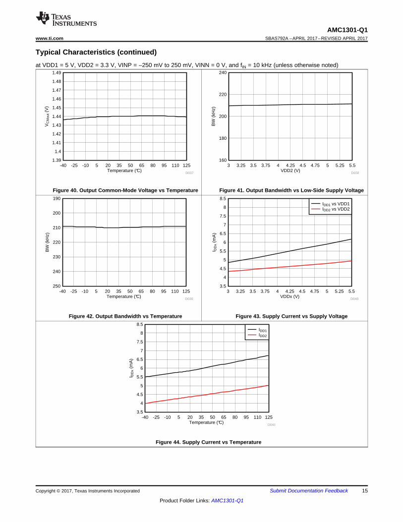
Typical Characteristics (continued)at VDD1 = 5 V, VDD2 = 3.3 V, VINP = –250 mV to 250 mV, VINN = 0 V, and fIN = 10 kHz (unless otherwise noted)
Figure 40. Output Common-Mode Voltage vs Temperature Figure 41. Output Bandwidth vs Low-Side Supply Voltage
Figure 42. Output Bandwidth vs Temperature Figure 43. Supply Current vs Supply Voltage
Figure 44. Supply Current vs Temperature

VINP - VINN
VOUTN
VOUTP
50% - 10%
0.5 V
0 V
90%
10%
50%
50%
50% - 50% 50% - 90%
VINP - VINN
VOUTN
VOUTP
0.5 V
0 V
90%
10%
tr tf
16
AMC1301-Q1SBAS792A –APRIL 2017–REVISED APRIL 2017 www.ti.com
Product Folder Links: AMC1301-Q1
Submit Documentation Feedback Copyright © 2017, Texas Instruments Incorporated
7 Parameter Measurement Information
7.1 Timing Diagrams
Figure 45. Rise and Fall Time Test Waveforms
Figure 46. Delay Time Test Waveforms

TX
Retiming and 4th-Order
Active Low-Pass
Filter
Isolation Barrier
û-Modulator
Band-GapReference
VOUTP
VOUTN
GND1
VINP
VINN
VDD1
AMC1301-Q1
+
±
RX
RX TX
Data
CLK
VDD2
GND2
Band-GapReference
Oscillator
Copyright © 2016, Texas Instruments Incorporated
17
AMC1301-Q1www.ti.com SBAS792A –APRIL 2017–REVISED APRIL 2017
Product Folder Links: AMC1301-Q1
Submit Documentation FeedbackCopyright © 2017, Texas Instruments Incorporated
8 Detailed Description
8.1 OverviewThe AMC1301-Q1 device is a fully-differential, precision, isolated amplifier. The input stage of the device consistsof a fully-differential amplifier that drives a second-order, delta-sigma (ΔΣ) modulator. The modulator uses theinternal voltage reference and clock generator to convert the analog input signal to a digital bitstream. Thedrivers (called TX in the Functional Block Diagram) transfer the output of the modulator across the isolationbarrier that separates the high-side and low-side voltage domains. The received bitstream and clock aresynchronized and processed by a fourth-order analog filter on the low-side and presented as a differential outputof the device, as shown in the Functional Block Diagram.
The SiO2-based, double-capacitive isolation barrier supports a high level of magnetic field immunity, as describedin ISO72x Digital Isolator Magnetic-Field Immunity. The digital modulation used in the AMC1301-Q1 device andthe isolation barrier characteristics result in high reliability and common-mode transient immunity.
8.2 Functional Block Diagram
8.3 Feature Description
8.3.1 Analog InputThe AMC1301-Q1 device incorporates front-end circuitry that contains a fully-differential amplifier followed by aΔΣ modulator sampling stage. The gain of the differential amplifier is set by internal precision resistors to a factorof 4 with a differential input impedance of 22 kΩ. Consider the input impedance of the AMC1301-Q1 device indesigns with high-impedance signal sources that may cause degradation of gain and offset specifications. Theimportance of this effect, however, depends on the desired system performance.
Additionally, the input bias current caused by the internal common-mode voltage at the output of the differentialamplifier causes an offset that is dependent on the actual amplitude of the input signal. See the Isolated VoltageSensing section for more details on reducing this effect.
There are two restrictions on the analog input signals (VINP and VINN). First, if the input voltage exceeds therange GND1 – 6 V to VDD1 + 0.5 V, then the input current must be limited to 10 mA because the device inputelectrostatic discharge (ESD) protection turns on. In addition, the linearity and noise performance of the deviceare ensured only when the analog input voltage remains within the specified linear full-scale range (FSR) andwithin the specified common-mode input voltage range.

18
AMC1301-Q1SBAS792A –APRIL 2017–REVISED APRIL 2017 www.ti.com
Product Folder Links: AMC1301-Q1
Submit Documentation Feedback Copyright © 2017, Texas Instruments Incorporated
Feature Description (continued)8.3.2 Fail-Safe OutputThe AMC1301-Q1 device offers a fail-safe output that simplifies diagnostics on system level. The fail-safe outputis active in two cases:• When the high-side supply VDD1 of the AMC1301-Q1 device is missing, or• When the common-mode input voltage, that is VCM = (VINP + VINN) / 2, exceeds the minimum common-
mode over-voltage detection level VCMov of VDD1 – 2 V.
The fail-safe output of the AMC1301-Q1 device is a negative differential output voltage value that differs from thenegative clipping output voltage, as shown in Figure 47 and Figure 48. As a reference value for the fail-safedetection on a system level, use the VFAILSAFE maximum value of –2.545 V.
Figure 47. Typical Negative Clipping Output of theAMC1301-Q1 Device
Figure 48. Typical Failsafe Output of the AMC1301-Q1Device
8.4 Device Functional ModesThe AMC1301-Q1 device is operational when the power supplies VDD1 and VDD2 are applied, as specified inRecommended Operating Conditions.
VOUTP
VOUTN
VDD2
GND2GND1
VINP
VINN
VDD1
AMC1301-Q1
HV+
HV-
To Load
FloatingPower Supply
15 V
3.3 V
RSHUNT
5.1 VR1
D1C1
10 F C2
0.1 F C4
0.1 F C5
2.2 F
ADC
Gate Driver
Gate Driver
TMS570L
Rei
nfor
ced
Isol
atio
n
R2
R3
C3
Copyright © 2016, Texas Instruments Incorporated
19
AMC1301-Q1www.ti.com SBAS792A –APRIL 2017–REVISED APRIL 2017
Product Folder Links: AMC1301-Q1
Submit Documentation FeedbackCopyright © 2017, Texas Instruments Incorporated
9 Application and Implementation
NOTEInformation in the following applications sections is not part of the TI componentspecification, and TI does not warrant its accuracy or completeness. TI’s customers areresponsible for determining suitability of components for their purposes. Customers shouldvalidate and test their design implementation to confirm system functionality.
9.1 Application InformationThe AMC1301-Q1 device offers unique linearity, high input common-mode and power-supply rejection, low acand dc errors, and low temperature drift. These features make the AMC1301-Q1 device a robust, high-performance, isolated amplifier for automotive applications where high voltage isolation is required.
9.2 Typical Applications
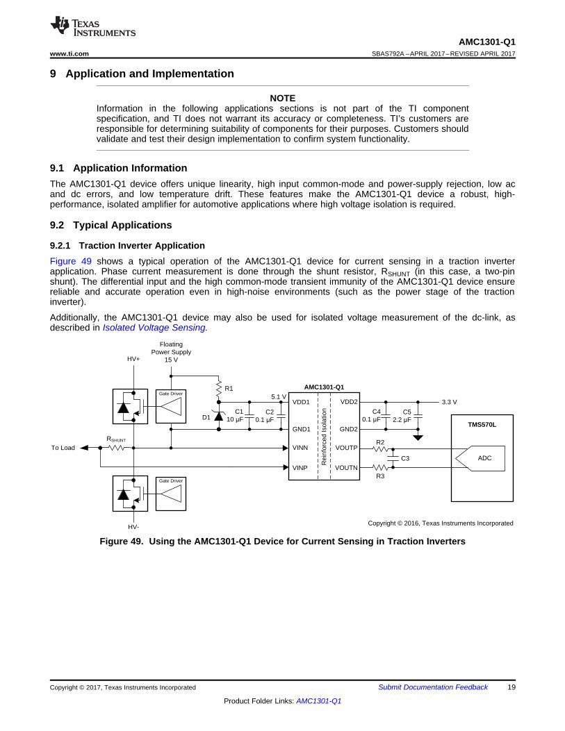
9.2.1 Traction Inverter ApplicationFigure 49 shows a typical operation of the AMC1301-Q1 device for current sensing in a traction inverterapplication. Phase current measurement is done through the shunt resistor, RSHUNT (in this case, a two-pinshunt). The differential input and the high common-mode transient immunity of the AMC1301-Q1 device ensurereliable and accurate operation even in high-noise environments (such as the power stage of the tractioninverter).
Additionally, the AMC1301-Q1 device may also be used for isolated voltage measurement of the dc-link, asdescribed in Isolated Voltage Sensing.
Figure 49. Using the AMC1301-Q1 Device for Current Sensing in Traction Inverters

20
AMC1301-Q1SBAS792A –APRIL 2017–REVISED APRIL 2017 www.ti.com
Product Folder Links: AMC1301-Q1
Submit Documentation Feedback Copyright © 2017, Texas Instruments Incorporated
Typical Applications (continued)9.2.1.1 Design RequirementsTable 1 lists the parameters for the typical application in Figure 49.
Table 1. Design RequirementsPARAMETER VALUE
High-side supply voltage 3.3 V or 5 VLow-side supply voltage 3.3 V or 5 V
Voltage drop across the shunt for a linear response ± 250 mV (maximum)
9.2.1.2 Detailed Design ProcedureThe high-side power supply (VDD1) for the AMC1301-Q1 device is derived from the power supply of the uppergate driver. Further details are provided in the Power Supply Recommendations section.
The floating ground reference (GND1) is derived from one of the ends of the shunt resistor that is connected tothe negative input of the AMC1301-Q1 device (VINN). If a four-pin shunt is used, the inputs of the AMC1301-Q1device are connected to the inner leads and GND1 is connected to one of the outer shunt leads.
Use Ohm's Law to calculate the voltage drop across the shunt resistor (VSHUNT) for the desired measuredcurrent: VSHUNT = I × RSHUNT.
Consider the following two restrictions to choose the proper value of the shunt resistor RSHUNT:• The voltage drop caused by the nominal current range must not exceed the recommended differential input
voltage range: VSHUNT ≤ ± 250 mV• The voltage drop caused by the maximum allowed overcurrent must not exceed the input voltage that causes
a clipping output: VSHUNT ≤ VClipping
For best performance, use an RC filter (components R2, R3, and C3 in Figure 49) to minimize the noise of thedifferential output signal. Tailor the bandwidth of this RC filter to the bandwidth requirement of the system. TIrecommends an NP0-type capacitor to be used for C3.
For more information on the general procedure to design the filtering and driving stages of SAR ADCs, consultthe TI Precision Designs 18-Bit, 1MSPS Data Acquisition Block (DAQ) Optimized for Lowest Distortion and Noise(SLAU515) and 18-Bit Data Acquisition Block (DAQ) Optimized for Lowest Power (SLAU513), available fordownload at www.ti.com.

Differential Input Voltage (mV)
Non
linea
rity
(%)
-250 -200 -150 -100 -50 0 50 100 150 200 250-0.03
-0.025
-0.02
-0.015
-0.01
-0.005
0
0.005
0.01
0.015
0.02
0.025
0.03
D024
VIN
VOUTP
VOUTN
21
AMC1301-Q1www.ti.com SBAS792A –APRIL 2017–REVISED APRIL 2017
Product Folder Links: AMC1301-Q1
Submit Documentation FeedbackCopyright © 2017, Texas Instruments Incorporated
9.2.1.3 Application CurvesIn traction inverter applications, the power switches must be protected in case of an overcurrent condition. Toallow for fast powering off of the system, a low delay caused by the isolated amplifier is required. Figure 50shows the typical full-scale step response of the AMC1301-Q1 device. Consider the delay of the required windowcomparator and the MCU to calculate the overall response time of the system.
Figure 50. Step Response of the AMC1301-Q1 Device
The high linearity and low temperature drift of offset and gain errors of the AMC1301-Q1 device, as shown inFigure 51, allows design of motor drives with low torque ripple.
Figure 51. Typical Nonlinearity of the AMC1301-Q1 Device

%100*'3'4
41(%) ¸
¹
ᬩ
§
RR
REG
3Gtot G
IN
RE E
R
û-Modulator
AMC1301-Q1 Front-End
VCM = 2 V
3.3 V or 5 V
High Voltage Potential
R1
R2
R3
R4 R5
R4' R5'
IIB
RIN
VDD1
VINP
VINN
GND1
R3'
+
±
Copyright © 2016, Texas Instruments Incorporated
22
AMC1301-Q1SBAS792A –APRIL 2017–REVISED APRIL 2017 www.ti.com
Product Folder Links: AMC1301-Q1
Submit Documentation Feedback Copyright © 2017, Texas Instruments Incorporated
9.2.2 Isolated Voltage SensingThe AMC1301-Q1 device is optimized for usage in current-sensing applications using low-impedance shunts.However, the device may also be used in isolated voltage-sensing applications if the effect of the (usually higher)impedance of the resistor divider used in this case is considered.
Figure 52. Using the AMC1301-Q1 Device for Isolated Voltage Sensing
9.2.2.1 Design RequirementsFigure 52 shows a simplified circuit typically used in high-voltage sensing applications. The high-impedanceresistors (R1 and R2) dominate the current value that flows through the resistive divider. The resistance of thesensing resistor R3 is chosen to meet the input voltage range of the AMC1301-Q1 device. This resistor and theinput impedance of the device (RIN = 18 kΩ) also create a voltage divider that results in an additional gain error.With the assumption of R1 and R2 having a considerably higher value than R3 and omitting R3' for the moment,the resulting total gain error is estimated using Equation 1, with EG being the initial gain error of the AMC1301-Q1 device.
(1)
This gain error may be easily minimized during the initial system-level gain calibration procedure.
9.2.2.2 Detailed Design ProcedureAs indicated in Figure 52, the output of the integrated differential amplifier is internally biased to a common-modevoltage of 2 V. This voltage results in a bias current IIB through the resistive network R4 and R5 (or R4' and R5')used for setting the gain of the amplifier. The value of this current is specified in the Pin Configuration andFunctions section. This bias current generates additional offset and gain errors that depend on the value of theresistor R3. Because the value of this bias current depends on the actual common-mode amplitude of the inputsignal (as shown in Figure 53), the initial system offset calibration eliminates the offset but not the gain errorcomponent. Therefore, in systems with high accuracy requirements, a series resistor is recommended to be usedat the negative input (VINN) of the AMC1301-Q1 device with a value equal to the shunt resistor R3 (that is, R3' =R3 in Figure 52) to eliminate the effect of the bias current.
This additional series resistor (R3') influences the gain error of the circuit. The effect is calculated usingEquation 2 with R4 = R4' = 12.5 kΩ. The effect of the internal resistors R5 = R5' cancels in this calculation.
(2)

VCM (V)
I IB (P
A)
-0.5 0 0.5 1 1.5 2 2.5 3-80
-60
-40
-20
0
20
40
60
D012
23
AMC1301-Q1www.ti.com SBAS792A –APRIL 2017–REVISED APRIL 2017
Product Folder Links: AMC1301-Q1
Submit Documentation FeedbackCopyright © 2017, Texas Instruments Incorporated
9.2.2.3 Application CurveFigure 53 shows the dependency of the input bias current on the common-mode voltage at the input of theAMC1301-Q1 device.
Figure 53. Input Current vs Input Common-Mode Voltage
9.3 Do's and Don'tsDo not leave the inputs of the AMC1301-Q1 device unconnected (floating) when the device is powered up. Ifboth device inputs are left floating, the input bias current drives them to the output common-mode of the analogfront-end of approximately 2 V. If the high-side supply voltage VDD1 is below 4 V, the internal common-modeovervoltage detector turns on and the output functions as described in the Fail-Safe Output section, which maylead to an undesired reaction on the system level.

VOUTP
VOUTN
VDD2
GND2GND1
VINP
VINN
VDD1
AMC1301-Q1
HV+
HV-
To Load
FloatingPower Supply
20 V
3.3 V or 5.0 V
RSHUNT
5.1 V
R1800
Z11N751A
C110 F
C20.1 F
C40.1 F
C52.2 F
Gate Driver
Gate DriverR
einf
orce
d Is
olat
ion
Copyright © 2016, Texas Instruments Incorporated
ADC121S101-Q1 12-Bit ADC
24
AMC1301-Q1SBAS792A –APRIL 2017–REVISED APRIL 2017 www.ti.com
Product Folder Links: AMC1301-Q1
Submit Documentation Feedback Copyright © 2017, Texas Instruments Incorporated
10 Power Supply RecommendationsIn a typical traction inverter application, the high-side power supply (VDD1) for the device is derived from thefloating power supply of the upper gate driver. For lowest cost, a Zener diode may be used to limit the voltage to5 V (or 3.3 V, depending on the design) ± 10%. Alternatively a low-cost, low-dropout (LDO) regulator (forexample, the LP2951-XX-Q1) may be used to minimize noise on the power supply. TI recommends a low-ESRdecoupling capacitor of 0.1 µF to filter this power-supply path. Place this capacitor (C2 in Figure 54) as close aspossible to the VDD1 pin of the AMC1301-Q1 device for best performance. If better filtering is required, anadditional 10-µF capacitor may be used. The floating ground reference (GND1) is derived from the end of theshunt resistor, which is connected to the negative input (VINN) of the device. If a four-pin shunt is used, thedevice inputs are connected to the inner leads, and GND1 is connected to one of the outer leads of the shunt.
To decouple the digital power supply on the controller side, use a 0.1-µF capacitor placed as close to the VDD2pin of the AMC1301-Q1 device as possible, followed by an additional capacitor from 1 µF to 10 µF.
Figure 54. Zener-Diode-Based, High-Side Power Supply

To Filteror ADC
Clearance area,to be kept free of any conductive materials.
AMC1301-Q1
VINP
VINN VOUTN
GND2
VOUTP
VDD2
0.1 µF
SMD0603
GND1
LEGEND
Copper Pour and Traces
High-Side Area
Low-Side Area
Via to Ground Plane
Via to Supply Plane
To Floating Power Supply
2.2 µF
SMD0603
Shu
nt R
esis
tor
VDD1
0.1 µF
SMD0603
Copyright © 2016, Texas Instruments Incorporated
25
AMC1301-Q1www.ti.com SBAS792A –APRIL 2017–REVISED APRIL 2017
Product Folder Links: AMC1301-Q1
Submit Documentation FeedbackCopyright © 2017, Texas Instruments Incorporated
11 Layout
11.1 Layout GuidelinesA layout recommendation showing the critical placement of the decoupling capacitors (as close as possible to theAMC1301-Q1 device) and placement of the other components required by the device is shown in Figure 55. Forbest performance, place the shunt resistor close to the VINP and VINN inputs of the AMC1301-Q1 device andkeep the layout of both connections symmetrical.
11.2 Layout Example
Figure 55. Recommended Layout of the AMC1301-Q1 Device

26
AMC1301-Q1SBAS792A –APRIL 2017–REVISED APRIL 2017 www.ti.com
Product Folder Links: AMC1301-Q1
Submit Documentation Feedback Copyright © 2017, Texas Instruments Incorporated
12 Device and Documentation Support
12.1 Documentation Support
12.1.1 Related DocumentationFor related documentation, see the following:• Isolation Glossary• ADC121S101-Q1 Single-Channel, 0.5 to 1-Msps, 12-Bit Analog-to-Digital Converter• LP2951-xx-Q1 Adjustable Micropower Voltage Regulators With Shutdown• TMS570LS0232 16- and 32-Bit RISC Flash Microcontroller• ISO72x Digital Isolator Magnetic-Field Immunity• 18-Bit, 1-MSPS Data Acquisition Block (DAQ) Optimized for Lowest Distortion and Noise• 18-Bit, 1-MSPS Data Acquisition Block (DAQ) Optimized for Lowest Power
12.2 Receiving Notification of Documentation UpdatesTo receive notification of documentation updates, navigate to the device product folder on ti.com. In the upperright corner, click on Alert me to register and receive a weekly digest of any product information that haschanged. For change details, review the revision history included in any revised document.
12.3 Community ResourcesThe following links connect to TI community resources. Linked contents are provided "AS IS" by the respectivecontributors. They do not constitute TI specifications and do not necessarily reflect TI's views; see TI's Terms ofUse.
TI E2E™ Online Community TI's Engineer-to-Engineer (E2E) Community. Created to foster collaborationamong engineers. At e2e.ti.com, you can ask questions, share knowledge, explore ideas and helpsolve problems with fellow engineers.
Design Support TI's Design Support Quickly find helpful E2E forums along with design support tools andcontact information for technical support.
12.4 TrademarksE2E is a trademark of Texas Instruments.All other trademarks are the property of their respective owners.
12.5 Electrostatic Discharge CautionThis integrated circuit can be damaged by ESD. Texas Instruments recommends that all integrated circuits be handled withappropriate precautions. Failure to observe proper handling and installation procedures can cause damage.
ESD damage can range from subtle performance degradation to complete device failure. Precision integrated circuits may be moresusceptible to damage because very small parametric changes could cause the device not to meet its published specifications.
12.6 GlossarySLYZ022 — TI Glossary.
This glossary lists and explains terms, acronyms, and definitions.
13 Mechanical, Packaging, and Orderable InformationThe following pages include mechanical, packaging, and orderable information. This information is the mostcurrent data available for the designated devices. This data is subject to change without notice and revision ofthis document. For browser-based versions of this data sheet, refer to the left-hand navigation.

PACKAGE OPTION ADDENDUM
www.ti.com 9-May-2017
Addendum-Page 1
PACKAGING INFORMATION
Orderable Device Status(1)
Package Type PackageDrawing
Pins PackageQty
Eco Plan(2)
Lead/Ball Finish(6)
MSL Peak Temp(3)
Op Temp (°C) Device Marking(4/5)
Samples
AMC1301QDWVQ1 ACTIVE SOIC DWV 8 64 Green (RoHS& no Sb/Br)
CU NIPDAU Level-3-260C-168 HR -40 to 125 1301Q1
AMC1301QDWVRQ1 ACTIVE SOIC DWV 8 1000 Green (RoHS& no Sb/Br)
CU NIPDAU Level-3-260C-168 HR -40 to 125 1301Q1
(1) The marketing status values are defined as follows:ACTIVE: Product device recommended for new designs.LIFEBUY: TI has announced that the device will be discontinued, and a lifetime-buy period is in effect.NRND: Not recommended for new designs. Device is in production to support existing customers, but TI does not recommend using this part in a new design.PREVIEW: Device has been announced but is not in production. Samples may or may not be available.OBSOLETE: TI has discontinued the production of the device.
(2) RoHS: TI defines "RoHS" to mean semiconductor products that are compliant with the current EU RoHS requirements for all 10 RoHS substances, including the requirement that RoHS substancedo not exceed 0.1% by weight in homogeneous materials. Where designed to be soldered at high temperatures, "RoHS" products are suitable for use in specified lead-free processes. TI mayreference these types of products as "Pb-Free".RoHS Exempt: TI defines "RoHS Exempt" to mean products that contain lead but are compliant with EU RoHS pursuant to a specific EU RoHS exemption.Green: TI defines "Green" to mean the content of Chlorine (Cl) and Bromine (Br) based flame retardants meet JS709B low halogen requirements of <=1000ppm threshold. Antimony trioxide basedflame retardants must also meet the <=1000ppm threshold requirement.
(3) MSL, Peak Temp. - The Moisture Sensitivity Level rating according to the JEDEC industry standard classifications, and peak solder temperature.
(4) There may be additional marking, which relates to the logo, the lot trace code information, or the environmental category on the device.
(5) Multiple Device Markings will be inside parentheses. Only one Device Marking contained in parentheses and separated by a "~" will appear on a device. If a line is indented then it is a continuationof the previous line and the two combined represent the entire Device Marking for that device.
(6) Lead/Ball Finish - Orderable Devices may have multiple material finish options. Finish options are separated by a vertical ruled line. Lead/Ball Finish values may wrap to two lines if the finishvalue exceeds the maximum column width.
Important Information and Disclaimer:The information provided on this page represents TI's knowledge and belief as of the date that it is provided. TI bases its knowledge and belief on informationprovided by third parties, and makes no representation or warranty as to the accuracy of such information. Efforts are underway to better integrate information from third parties. TI has taken andcontinues to take reasonable steps to provide representative and accurate information but may not have conducted destructive testing or chemical analysis on incoming materials and chemicals.TI and TI suppliers consider certain information to be proprietary, and thus CAS numbers and other limited information may not be available for release.
In no event shall TI's liability arising out of such information exceed the total purchase price of the TI part(s) at issue in this document sold by TI to Customer on an annual basis.

PACKAGE OPTION ADDENDUM
www.ti.com 9-May-2017
Addendum-Page 2
OTHER QUALIFIED VERSIONS OF AMC1301-Q1 :
• Catalog: AMC1301
NOTE: Qualified Version Definitions:
• Catalog - TI's standard catalog product

TAPE AND REEL INFORMATION
*All dimensions are nominal
Device PackageType
PackageDrawing
Pins SPQ ReelDiameter
(mm)
ReelWidth
W1 (mm)
A0(mm)
B0(mm)
K0(mm)
P1(mm)
W(mm)
Pin1Quadrant
AMC1301QDWVRQ1 SOIC DWV 8 1000 330.0 16.4 12.05 6.15 3.3 16.0 16.0 Q1
PACKAGE MATERIALS INFORMATION
www.ti.com 19-Apr-2017
Pack Materials-Page 1

*All dimensions are nominal
Device Package Type Package Drawing Pins SPQ Length (mm) Width (mm) Height (mm)
AMC1301QDWVRQ1 SOIC DWV 8 1000 367.0 367.0 38.0
PACKAGE MATERIALS INFORMATION
www.ti.com 19-Apr-2017
Pack Materials-Page 2
www.ti.com
PACKAGE OUTLINE
C
TYP11.5 0.25
2.8 MAX
TYP0.330.13
0 -8
6X 1.27
8X 0.510.31
2X3.81
0.460.36
1.00.5
0.25GAGE PLANE
A
NOTE 3
5.955.75
BNOTE 4
7.67.4
(2.286)
(2)
4218796/A 09/2013
SOIC - 2.8 mm max heightDWV0008ASOIC
NOTES: 1. All linear dimensions are in millimeters. Dimensions in parenthesis are for reference only. Dimensioning and tolerancing per ASME Y14.5M. 2. This drawing is subject to change without notice. 3. This dimension does not include mold flash, protrusions, or gate burrs. Mold flash, protrusions, or gate burrs shall not exceed 0.15 mm, per side. 4. This dimension does not include interlead flash. Interlead flash shall not exceed 0.25 mm, per side.
18
0.25 C A B
54
AREAPIN 1 ID
SEATING PLANE
0.1 C
SEE DETAIL A
DETAIL ATYPICAL
SCALE 2.000

www.ti.com
EXAMPLE BOARD LAYOUT
(10.9)
0.07 MAXALL AROUND
0.07 MINALL AROUND
8X (1.8)
8X (0.6)
6X (1.27)
4218796/A 09/2013
SOIC - 2.8 mm max heightDWV0008ASOIC
SYMM
SYMM
SEE DETAILS
LAND PATTERN EXAMPLE9.1 mm NOMINAL CLEARANCE/CREEPAGE
SCALE:6X
NOTES: (continued) 5. Publication IPC-7351 may have alternate designs. 6. Solder mask tolerances between and around signal pads can vary based on board fabrication site.
METAL SOLDER MASKOPENING
NON SOLDER MASKDEFINED
SOLDER MASK DETAILS
OPENINGSOLDER MASK METAL
SOLDER MASKDEFINED

www.ti.com
EXAMPLE STENCIL DESIGN
8X (1.8)
8X (0.6)
6X (1.27)
(10.9)
4218796/A 09/2013
SOIC - 2.8 mm max heightDWV0008ASOIC
NOTES: (continued) 7. Laser cutting apertures with trapezoidal walls and rounded corners may offer better paste release. IPC-7525 may have alternate design recommendations. 8. Board assembly site may have different recommendations for stencil design.
SOLDER PASTE EXAMPLEBASED ON 0.125 mm THICK STENCIL
SCALE:6X
SYMM
SYMM

IMPORTANT NOTICE
Texas Instruments Incorporated (TI) reserves the right to make corrections, enhancements, improvements and other changes to itssemiconductor products and services per JESD46, latest issue, and to discontinue any product or service per JESD48, latest issue. Buyersshould obtain the latest relevant information before placing orders and should verify that such information is current and complete.TI’s published terms of sale for semiconductor products (http://www.ti.com/sc/docs/stdterms.htm) apply to the sale of packaged integratedcircuit products that TI has qualified and released to market. Additional terms may apply to the use or sale of other types of TI products andservices.Reproduction of significant portions of TI information in TI data sheets is permissible only if reproduction is without alteration and isaccompanied by all associated warranties, conditions, limitations, and notices. TI is not responsible or liable for such reproduceddocumentation. Information of third parties may be subject to additional restrictions. Resale of TI products or services with statementsdifferent from or beyond the parameters stated by TI for that product or service voids all express and any implied warranties for theassociated TI product or service and is an unfair and deceptive business practice. TI is not responsible or liable for any such statements.Buyers and others who are developing systems that incorporate TI products (collectively, “Designers”) understand and agree that Designersremain responsible for using their independent analysis, evaluation and judgment in designing their applications and that Designers havefull and exclusive responsibility to assure the safety of Designers' applications and compliance of their applications (and of all TI productsused in or for Designers’ applications) with all applicable regulations, laws and other applicable requirements. Designer represents that, withrespect to their applications, Designer has all the necessary expertise to create and implement safeguards that (1) anticipate dangerousconsequences of failures, (2) monitor failures and their consequences, and (3) lessen the likelihood of failures that might cause harm andtake appropriate actions. Designer agrees that prior to using or distributing any applications that include TI products, Designer willthoroughly test such applications and the functionality of such TI products as used in such applications.TI’s provision of technical, application or other design advice, quality characterization, reliability data or other services or information,including, but not limited to, reference designs and materials relating to evaluation modules, (collectively, “TI Resources”) are intended toassist designers who are developing applications that incorporate TI products; by downloading, accessing or using TI Resources in anyway, Designer (individually or, if Designer is acting on behalf of a company, Designer’s company) agrees to use any particular TI Resourcesolely for this purpose and subject to the terms of this Notice.TI’s provision of TI Resources does not expand or otherwise alter TI’s applicable published warranties or warranty disclaimers for TIproducts, and no additional obligations or liabilities arise from TI providing such TI Resources. TI reserves the right to make corrections,enhancements, improvements and other changes to its TI Resources. TI has not conducted any testing other than that specificallydescribed in the published documentation for a particular TI Resource.Designer is authorized to use, copy and modify any individual TI Resource only in connection with the development of applications thatinclude the TI product(s) identified in such TI Resource. NO OTHER LICENSE, EXPRESS OR IMPLIED, BY ESTOPPEL OR OTHERWISETO ANY OTHER TI INTELLECTUAL PROPERTY RIGHT, AND NO LICENSE TO ANY TECHNOLOGY OR INTELLECTUAL PROPERTYRIGHT OF TI OR ANY THIRD PARTY IS GRANTED HEREIN, including but not limited to any patent right, copyright, mask work right, orother intellectual property right relating to any combination, machine, or process in which TI products or services are used. Informationregarding or referencing third-party products or services does not constitute a license to use such products or services, or a warranty orendorsement thereof. Use of TI Resources may require a license from a third party under the patents or other intellectual property of thethird party, or a license from TI under the patents or other intellectual property of TI.TI RESOURCES ARE PROVIDED “AS IS” AND WITH ALL FAULTS. TI DISCLAIMS ALL OTHER WARRANTIES ORREPRESENTATIONS, EXPRESS OR IMPLIED, REGARDING RESOURCES OR USE THEREOF, INCLUDING BUT NOT LIMITED TOACCURACY OR COMPLETENESS, TITLE, ANY EPIDEMIC FAILURE WARRANTY AND ANY IMPLIED WARRANTIES OFMERCHANTABILITY, FITNESS FOR A PARTICULAR PURPOSE, AND NON-INFRINGEMENT OF ANY THIRD PARTY INTELLECTUALPROPERTY RIGHTS. TI SHALL NOT BE LIABLE FOR AND SHALL NOT DEFEND OR INDEMNIFY DESIGNER AGAINST ANY CLAIM,INCLUDING BUT NOT LIMITED TO ANY INFRINGEMENT CLAIM THAT RELATES TO OR IS BASED ON ANY COMBINATION OFPRODUCTS EVEN IF DESCRIBED IN TI RESOURCES OR OTHERWISE. IN NO EVENT SHALL TI BE LIABLE FOR ANY ACTUAL,DIRECT, SPECIAL, COLLATERAL, INDIRECT, PUNITIVE, INCIDENTAL, CONSEQUENTIAL OR EXEMPLARY DAMAGES INCONNECTION WITH OR ARISING OUT OF TI RESOURCES OR USE THEREOF, AND REGARDLESS OF WHETHER TI HAS BEENADVISED OF THE POSSIBILITY OF SUCH DAMAGES.Unless TI has explicitly designated an individual product as meeting the requirements of a particular industry standard (e.g., ISO/TS 16949and ISO 26262), TI is not responsible for any failure to meet such industry standard requirements.Where TI specifically promotes products as facilitating functional safety or as compliant with industry functional safety standards, suchproducts are intended to help enable customers to design and create their own applications that meet applicable functional safety standardsand requirements. Using products in an application does not by itself establish any safety features in the application. Designers mustensure compliance with safety-related requirements and standards applicable to their applications. Designer may not use any TI products inlife-critical medical equipment unless authorized officers of the parties have executed a special contract specifically governing such use.Life-critical medical equipment is medical equipment where failure of such equipment would cause serious bodily injury or death (e.g., lifesupport, pacemakers, defibrillators, heart pumps, neurostimulators, and implantables). Such equipment includes, without limitation, allmedical devices identified by the U.S. Food and Drug Administration as Class III devices and equivalent classifications outside the U.S.TI may expressly designate certain products as completing a particular qualification (e.g., Q100, Military Grade, or Enhanced Product).Designers agree that it has the necessary expertise to select the product with the appropriate qualification designation for their applicationsand that proper product selection is at Designers’ own risk. Designers are solely responsible for compliance with all legal and regulatoryrequirements in connection with such selection.Designer will fully indemnify TI and its representatives against any damages, costs, losses, and/or liabilities arising out of Designer’s non-compliance with the terms and provisions of this Notice.
Mailing Address: Texas Instruments, Post Office Box 655303, Dallas, Texas 75265Copyright © 2017, Texas Instruments Incorporated


![SD servicio nombres docu examen2 - UPM · 2019. 4. 9. · d urrw vhuyhuv qhw =rqd d qlf hv =rqd hv hlqvwhlq ffxsp xsp hv =rqd xsp hv ]dsh il xsp hv =rqd il xsp hv qv jqx ruj =rqd](https://img.dokumen.tips/doc/110x75/613bce56f8f21c0c826934b2/sd-servicio-nombres-docu-examen2-upm-2019-4-9-d-urrw-vhuyhuv-qhw-rqd-d-qlf.jpg)

![SD servicio nombres docu examen2 - UPMlaurel.datsi.fi.upm.es/_media/.../sd/...examen-4pp.pdfd urrw vhuyhuv qhw =rqd d qlf hv =rqd hv hlqvwhlq ffxsp xsp hv =rqd xsp hv ]dsh il xsp hv](https://img.dokumen.tips/doc/110x75/5fdd3be9af48e220dc67f7d6/sd-servicio-nombres-docu-examen2-d-urrw-vhuyhuv-qhw-rqd-d-qlf-hv-rqd-hv-hlqvwhlq.jpg)