Embed Size (px)
Citation preview


Introduction
• Originally, it was the development of the standard bipolarNPN and substrate lateral PNP transistors
• Process extensions:allows standard bipolar to fabricate NPN transistors
with extremely high betas and lateral PNP transistors withimproved high-current performance
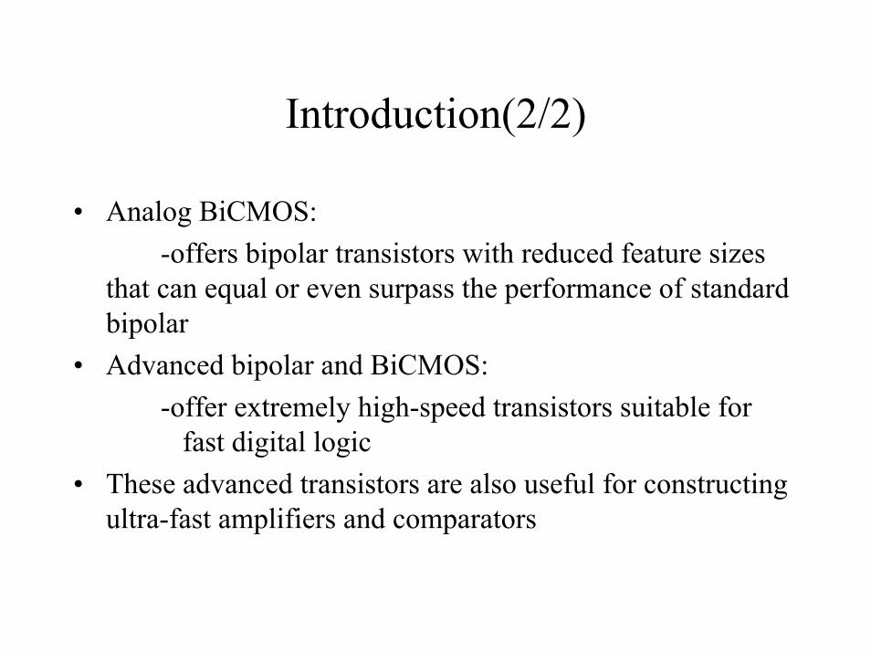
Introduction(2/2)
• Analog BiCMOS:-offers bipolar transistors with reduced feature sizes
that can equal or even surpass the performance of standardbipolar
• Advanced bipolar and BiCMOS:-offer extremely high-speed transistors suitable for
fast digital logic• These advanced transistors are also useful for constructing
ultra-fast amplifiers and comparators

Extensions to standard bipolar
• Standard bipolar was perfected in the 60s• Many other processes have been developed since then that
offer superior device performance, but most of them haveproven to be too costly or too complex to justify theirwidespread adoption
• Two options that have enjoyed some measure of popularityare the super-beta NPN and the deep-P+ lateral PNP
• Only real advantages of standard bipolar are its simplicityand its low cost

Super-beta NPN(1/2)
• Employs a deeper emitter diffusion that decreases thewidth of the neutral base to less than 0.1um, which allowsBetas in excess of 5000 are possible
• The thin, lightly doped base punches through at collector-to-emitter voltages of only 1 to 3V, and early voltages liein the same range, these limitations restrict super-betatransistors to a few specialized applications
• Alternatives like BiFET and BiCMOS can replace super-beta transistors, but it ramains cost saving to use super-betatransistors in older products

Super-beta NPN(2/2)
• Comparison of cross sections of standard bipolar NPN anda super-beta NPN

Deep-P+ lateral PNP(1/2)
• Employs a special deep-P+ diffusion that is more heavilydoped and deeper than the regular base diffusion
• The increase in dopant concentration improves the emitterinjection efficiency
• The deeper junction ensures that a larger percentage ofemitter injection occurs from the sidewalls
• Deep-P+ laterals can operate at current densities two orthree times as large as base laterals

Deep-P+ lateral PNP(2/2)
• Comparison of cross sections of a standard bipolar lateralPNP and a deep-P+ lateral PNP

Analog BiCMOS BipolarTransistors(1/8)
• Analog BiCMOS process employs a P-type9(100) epiinstead of the N-type(111) epi favored by standard bipolar
• Components must occupy N-wells isolated from oneanother by regions of P-epi
• Except for the substitution of N-wells for N-tanks, theconstruction of bipolar devices in analog BiCMOSparallels that in standard bipolar

Analog BiCMOS BipolarTransistors(2/8)
• Difficulties of using N-well to form the collector of theNPN(CDI NPN):
-the nature of the well causes the resistivity of itslowest portions to greatly exceed the resistivity of standardbipolar N-epi
-the vertical resistance through the N-well is muchgreater than the vertical resistance through the standardbipolar N-epi
-without deep-N+ sinker, the vertical collectorresistance will cause a soft transition from saturation tonormal active operation
-shallow junction depth of N-well limits theoperating voltage to 15 to 20V

Analog BiCMOS BipolarTransistors(3/8)
• Comparison of saturation characteristics of CDI NPNtransistors with and without the addition of deep N+ sinker
Analog BiCMOS BipolarTransistors(4/8)
• Extended-base transistor:-does not employ N-well in its construction-base consists of the base diffusion and an isolated P-
epi region-a ring of deep-N+ isolates the base from the
surrounding P-epi, which also allows contact to the NBL-collector consists of the NBL beneath its extended
base and the deep-N+ ring surrounding it the extendedbase structure has a higher planar base-collectorbreakdown voltage then the CDI NPN, resulting in ahigher Vceo ranging from 40 to 60V

Analog BiCMOS BipolarTransistors(5/8)
• Layout and cross section of an extended-base NPNtransistor

Analog BiCMOS BipolarTransistors(6/8)
• If the base diffusion was eliminated:-it will form the epi-base transistor-resulting in a reduced Gummel number-epi-base transistor offers a high beta at the cost of
reduced operating voltage and increased base resistance-epi-base transistor does not require a separate base
diffusion
Analog BiCMOS BipolarTransistors(7/8)
• Analog BiCMOS substrate PNP:-employs an emitter constructed of PSD rather then
base-larger junction depth of the base diffusion reduces the
punchthrough voltage of the transistor-substrate PNP transistors inject current into the
substrate, the designer must take precautions to avoidsubstrate biasing

Analog BiCMOS BipolarTransistors(8/8)
• Lateral PNP transistors:-exhibits high peak betas-relative shallowness of the base diffusion allows the
emitter n collector to be placed in close proximity to oneanother and the graded nature of the well helps increase thepunchthrough voltage near the surface where the base isnarrowest


•We can produce substrate PNP using N-well CMOSprocess.•Similarities between the substrate PNP and BiCMOS:Emitter from PSD,Base from N-well,Collector from P-substrate•Performance is less than that of a BiCMOS device:
–Difference in N-well doping–Use of shallow clad moats

•N-well doping:–In CDI NPN: lightly doped, acts as the drift region.–In lateral & substrate PNP: acts as the base region.–In High voltage long channel PNP transistors it forms abackgate.
•In modern CMOS process: Channel length is less than 1micron•We use higher doping of the well to prevent punchthrough•Draw back: reducing the gain of the substrate PNP

MOS structure:
•Thin S/D implants in short channel MOS trans. Reducesemitter injection efficiency
•Bad idea to use clad moat in silicidation process assilicidation consumes the silicon layer in the S/D implants andtherefore thins the already thin S/D diffusion.

Bipolar Transistors in a CMOS Process(4/7)
•The gain of the PNP transistor vary from less than 1 to more than50.
•Variations in Beta ß produce variations in base current.
•Collector current mismatches of 3 to 5% are common in low gainCMOS substrate transistors.
•Even though this variation is small, it becomes more obvious whenBeta ß reaches unity.

Layout of Substrate PNP transistors in N-well CMOSprocess:• Silicide block mask is coded over the emitter region.•Minimum width NSD and PSD strips are interchanged,thus reducing the resistance of the base of the transistor andhelp reduces base current variation in matching process

•There has been attempts to construct lateral PNPtransistors in straight CMOS processes.•These were proved to be unsuccessful because of lowgain, low collector efficiency, and a value of Betareaching unity which prevents matching processes.•A solution is to use Polysilicon to construct the baseregion•Drawback: large variation in Beta still exist

•An alternative to lateral PNP transistors can befabricated by the presence of the NBL.•The resulting transistor can not handle high currents asa result of high resistivity collectors, but they showbetter performance than other CMOS process devices


• Limits on switching speeds– Junction capacitance– Base resistance– Neutral base width
• Switching transistors• Transit time limitations

Washed-emitter
• Simplest way to educejunction capacitance?
• Smaller geometriesusing improvedphotolithography

Polysilicon Emitter
• Deposition of arsenic-doped polysilicon• Thin and heavily doped emitter diffusion• Betas of six or more times greater


• Polysilicon emitters are universally used in BiCMOStechnologies as part of the silicon bipolar transistorsor SiGe heterojunction bipolar transistors. Polysiliconemitters have a number of important advantages:– Improved gain.– Scalability to deep sub-micron geometries.– Can be used in self-aligned fabrication schemes that
minimise parasitic capacitance and resistance� Compatibility with CMOS.

• LOCOS prosses to oxidize– Less collector substrate capacitance– Shrinks tank dimensions
• Listen and write this down �

Polysilicon Emitter
• Increased emitter junction efficiency– Grain boundaries in the polysilicon– Thin interfacial oxide
• Heavily doped base region• Precise emitter junctions• Conclusion

Super Self-aligned
• Dual or hybrid• Base and emitter use doped polysilicon• 250ps (WHOAA that’s fast!)• Complexity limits application