Embed Size (px)
Citation preview
Page 1
Altair 8800c Front Panel Board Set Ver 1.2, Feb 2019
Introduction
The Altair 8800c front panel
board set is a drop-in re-
placement for the original Al-
tair 8800 front panel board.
The new board set was creat-
ed for the following reasons:
1) Availability
Finding an original front panel board to restore
or build an Altair is nearly impossible. The new
board set provides a drop-in equivalent that is
readily available.
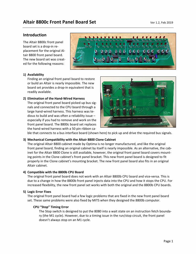
2) Elimination of the Hand-Wired Harness
The original front panel board picked up bus sig-
nals and connected to the CPU board through a
large hand-wired harness. This harness was te-
dious to build and was often a reliability issue –
especially if you had to remove and work on the
front panel board. The 8800c board set replaces
the hand-wired harness with a 50 pin ribbon ca-
ble that connects to a bus interface board (shown here) to pick up and drive the required bus signals.
3) Mechanical Compatibility with the Altair 8800 Clone Cabinet
The original Altair 8800 cabinet made by Optima is no longer manufactured, and like the original
front panel board, finding an original cabinet by itself is nearly impossible. As an alternative, the cab-
inet for the Altair 8800 Clone is still available, however, the original front panel board covers mount-
ing points in the Clone cabinet’s front panel bracket. This new front panel board is designed to fit
properly in the Clone cabinet’s mounting bracket. The new front panel board also fits in an original
Altair cabinet.
4) Compatible with the 8800b CPU Board
The original front panel board does not work with an Altair 8800b CPU board and vice-versa. This is
due to a change in how the 8800b front panel injects data into the CPU and how it stops the CPU. For
increased flexibility, the new front panel set works with both the original and the 8800b CPU boards.
5) Logic Error Fixes
The original front panel board had a few logic problems that are fixed in the new front panel board
set. These same problems were also fixed by MITS when they designed the 8800b computer.
CPU “Stop” Timing Error
The Stop switch is designed to put the 8080 into a wait state on an instruction fetch bounda-
ry (the M1 cycle). However, due to a timing issue in the run/stop circuit, the front panel
doesn’t always stop on an M1 cycle.

Page 2
Indeterminate Power-On State
On power-on, the run/stop flip-flop on the front panel board is not initialized and the 8080
processor is not given a reset signal. These omissions tend to leave the 8080 in an invalid
state on power-on. This is why the “STOP/RESET” switch sequence is required to put the
computer into a valid state. This fix can be optionally enabled or left like the original.
Reset not Synchronized with phi2
An undocumented 8080 reset timing requirement is that reset be released a minimum of
about 200ns prior to the rising edge of phi2. This is implemented in the Intel 8224 clock gen-
erator that was used on the 8800b CPU board, but this chip is not used on the original Altair
CPU board. The new front panel board enforces this timing for resets generated by the front
panel.
Front Panel PRDY Output is not Open Collector
Clients on the bus should drive the PRDY signal with an open collector driver. The signal is
terminated on the CPU board with a 1K pull-up resistor. However, the original front panel
board actively drives this signal high. Therefore, when any bus client drives PRDY low to in-
sert wait states, its output driver is sinking the active high drive of the front panel’s PRDY
driver.
6) Enhancements
In addition to duplicating the functionality of the original front panel board, the 8800c front panel
board set offers several enhancements that can be optionally enabled:
• An output latch at I/O address 0FFh that can display on the data LEDs (similar to IMSAI 8080)
• Auto repeat single-step at selectable rate from 1hz-8hz, similar to the 8800b
• Code snippet injection: Common Altair bootstrap loaders, port echo routines, Kill-the-Bit, etc.
can be injected into RAM by selecting the desired code snippet on the lower eight address
switches, then depressing the AUX-Left switch.
• Auto jump on power-on (can be independent of reset operation)
• Auto jump on reset (can be independent of power-on operation)
Page 3
Front Panel Board Assembly
Assembly of the front panel board is not a beginner’s project and these instructions won’t teach you
how to solder components on a PCB, solder connectors, or show you the difference between a resistor
and a diode. If you have any concerns about building this board, please contact me first.
Many assembly details are illustrated in photographs that follow. Rather than print this manual, you
may want to view this document on your tablet while you work. A tablet makes it especially easy to
zoom into the photos to see the details you may need.
Parts List Designator Description Part Number Distributor
C1-C5 0.1uf, 50v 2146302 Jameco
C6 100uf, 16v electrolytic 647-TVX1C101MAD Mouser
D1-D36 Red LED Everlite HLMPD150A Digi-Key 1080-1064-ND
J1 50 pin, dual row IDC straight header 517-D3433-6302-AR Mouser
J2 5-pin, 0.156 locking header B5P-VH-B-LFSN Digi-Key 455-1642-ND
Female Housing VHR-5N Digi-Key 455-1186-ND
Crimp Pins SVH-21T-P1.1 Digi-Key 455-1133-1-ND
IC-A,B,C,D,E 74LS165 Parallel In Shift Register 595-SN74LS165AN Mouser
R1-R36 2K, 1/4w, 5% 291-2K-RC Mouser
R37-R52 4.3K,1/4w, 5% 291-4.3K-RC Mouser
S1 Toggle Switch On-None-On (Silver) APEM 5236AB Search for best deal
S10-S25 Toggle Switch On-None-On (Gold) APEM 5236CDB Search for best deal
S2-S9 Toggle Switch (On)-Off-(On) (Gold) APEM 5237CDB Search for best deal
Switches
If at all possible, do not use C&K switches for the front panel. The C&K switches have an erratic and stiff
feel – especially the momentary switches – compared to the American Switch brand used in the original
Altair. In addition, I’ve had several C&K switches break while gently tightening the bushing nut as well as
during normal use. The APEM switch part numbers listed above are much closer to the original American
Switch brand. In fact, APEM purchased American Switch a number of years ago.
The power switch must have silver contacts as noted for S1. Ideally, use gold contacts for all remaining
switches. Do not mix switch brands as most have slightly different body heights and this causes prob-
lems when mounting the front panel to the mounting plate/bracket.
The APEM switches can be expensive. I may be able to help with a bulk buy. Contact me if interested.
Additional Part Notes
Use only LS-TTL parts. Some IC inputs are tied directly to Vcc. Multi-emitter TTL inputs do not tolerate
this well (e.g., 74xxx and 74Sxxx).
The specified LEDs provide an appropriate brightness with the 2K resistors specified for R1-R36. You may
need to choose a different resistor value if a different LED is used.
Page 4
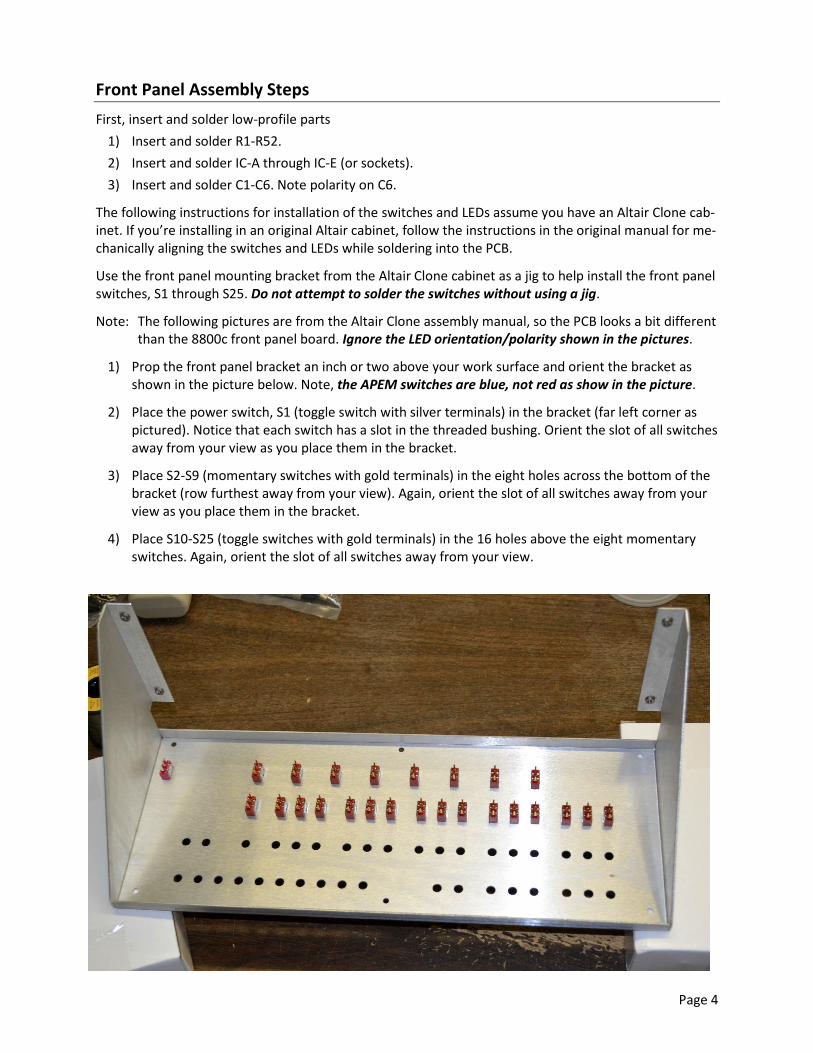
Front Panel Assembly Steps
First, insert and solder low-profile parts
1) Insert and solder R1-R52.
2) Insert and solder IC-A through IC-E (or sockets).
3) Insert and solder C1-C6. Note polarity on C6.
The following instructions for installation of the switches and LEDs assume you have an Altair Clone cab-
inet. If you’re installing in an original Altair cabinet, follow the instructions in the original manual for me-
chanically aligning the switches and LEDs while soldering into the PCB.
Use the front panel mounting bracket from the Altair Clone cabinet as a jig to help install the front panel
switches, S1 through S25. Do not attempt to solder the switches without using a jig.
Note: The following pictures are from the Altair Clone assembly manual, so the PCB looks a bit different
than the 8800c front panel board. Ignore the LED orientation/polarity shown in the pictures.
1) Prop the front panel bracket an inch or two above your work surface and orient the bracket as
shown in the picture below. Note, the APEM switches are blue, not red as show in the picture.
2) Place the power switch, S1 (toggle switch with silver terminals) in the bracket (far left corner as
pictured). Notice that each switch has a slot in the threaded bushing. Orient the slot of all switches
away from your view as you place them in the bracket.
3) Place S2-S9 (momentary switches with gold terminals) in the eight holes across the bottom of the
bracket (row furthest away from your view). Again, orient the slot of all switches away from your
view as you place them in the bracket.
4) Place S10-S25 (toggle switches with gold terminals) in the 16 holes above the eight momentary
switches. Again, orient the slot of all switches away from your view.
Page 5
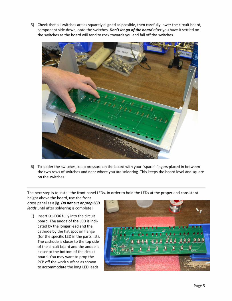
5) Check that all switches are as squarely aligned as possible, then carefully lower the circuit board,
component side down, onto the switches. Don’t let go of the board after you have it settled on
the switches as the board will tend to rock towards you and fall off the switches.
6) To solder the switches, keep pressure on the board with your “spare” fingers placed in between
the two rows of switches and near where you are soldering. This keeps the board level and square
on the switches.
The next step is to install the front panel LEDs. In order to hold the LEDs at the proper and consistent
height above the board, use the front
dress panel as a jig. Do not cut or prep LED
leads until after soldering is complete!
1) Insert D1-D36 fully into the circuit
board. The anode of the LED is indi-
cated by the longer lead and the
cathode by the flat spot on flange
(for the specific LED in the parts list).
The cathode is closer to the top side
of the circuit board and the anode is
closer to the bottom of the circuit
board. You may want to prop the
PCB off the work surface as shown
to accommodate the long LED leads.

Page 6
2) Work the front dress panel over the switches and then down the switch bushings slightly. You
don’t need to push the panel all the way down to the switch body.
3) Turn the PCB/front panel over as shown below and let the LEDs fall into the front panel LED holes.
If the front panel sags a bit in the middle, add a third support point near the middle of the panel.
4) Carefully adjust the spacing between the PCB and the front panel in order to accommodate the
four 5/8” spacers provided*. The goal is to make the PCB and front panel as parallel as possible.
The spacers are used only for this step – they do not remain in the assembly. (Note that once an
LED is soldered, it can then serve as a “spacer”) See the pictures on the next page.
5) Push each LED all the way down into its corresponding front panel hole. Re-verify that the front
panel and PCB look perfectly parallel to each other and are resting directly on all of the white
spacers. See the pictures on the next page.
6) Solder the LEDs: Press down gently on the PCB with your “spare” fingers as you solder the LEDs to
the PCB. You may want to slide the white spacers near the area you are working as you proceed
through the LEDs. Note that once an LED is soldered, it can then serve as a “spacer.”
* The spacer height determines how far the LEDs will protrude through the front panel after final as-
sembly. With APEM switches in the Altair Clone case, a spacer height of 5/8” to 11/16” gives a good
LED position after final assembly. At 5/8”, the LEDs protrude just slightly through the front panel. At
11/16”, the LEDs protrude a bit further. You can add something thin under each 5/8” spacer to raise it
towards 11/16” depending on your LED position preference. The spacing requirement is different if
you use a different switch brand since switch body height varies slightly between brands.

Page 7
Lastly, install J1 and J2 on the back side of the circuit board.
J1 – Note the orientation of the keying slot before soldering the connector onto the board. Again, the
connector goes on the back side of the board.
J2 – Though not a requirement, I’d recommend pulling the center pin out of the J2 connector. If you
leave the pin in place, note that its hole on the PCB is not plated and should not be soldered.
Page 8
Final Assembly (using an Altair Clone cabinet)
Mount the circuit board to the front panel support bracket.
1) Set all toggle switches in the
down position. Feed the
switch batons into the holes
through the rear of the sup-
port bracket. Be sure the
bracket is fully seated
against the body of every
switch. You may have to
squeeze/push the panel
firmly around a few of the
switches to free those spots
where the support bracket
may be caught on the
switch threads.
2) Install a lock washer and nut (finger tighten only) on the power switch, all eight momentary
switches, and every other address switch (A14, A12, A10,… down to A0) as highlighted below.
3) Incrementally tighten nuts – one on the far left, then one on the far right, working back to the
middle, then repeat tightening each nut a bit more. A 5/16” deep socket makes this job much
easier. Do not over-tighten the nuts – trust the lock washer.
Page 9
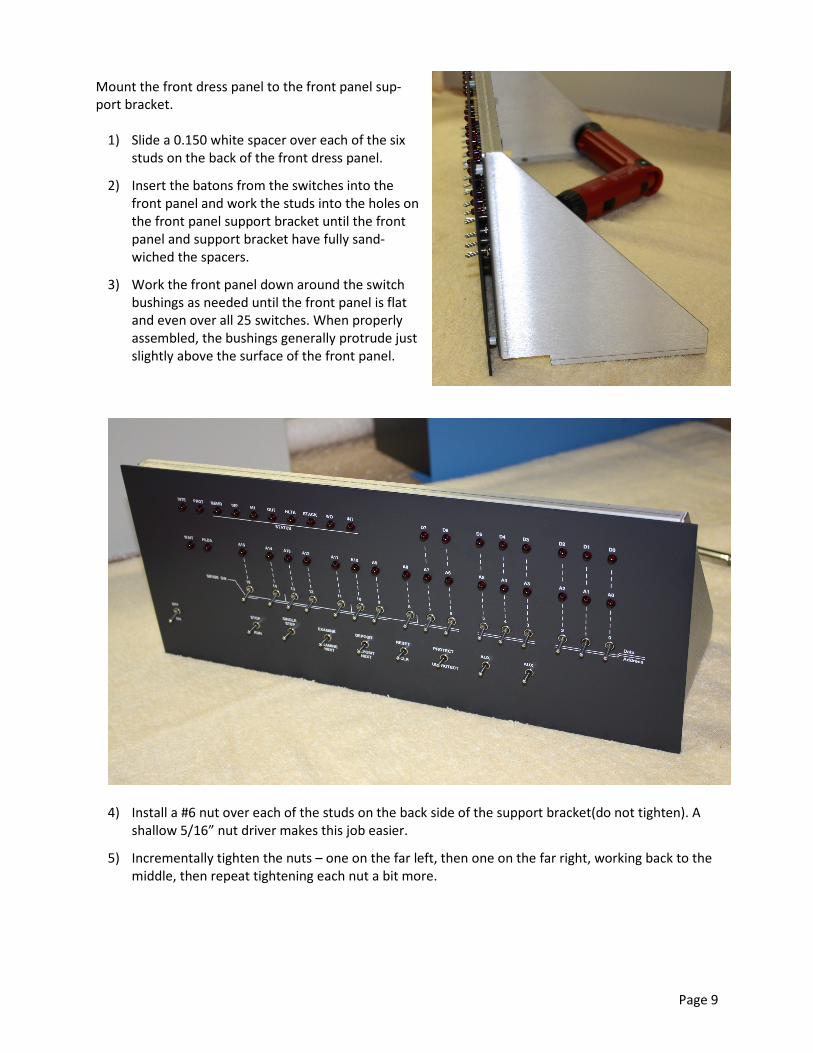
Mount the front dress panel to the front panel sup-
port bracket.
1) Slide a 0.150 white spacer over each of the six
studs on the back of the front dress panel.
2) Insert the batons from the switches into the
front panel and work the studs into the holes on
the front panel support bracket until the front
panel and support bracket have fully sand-
wiched the spacers.
3) Work the front panel down around the switch
bushings as needed until the front panel is flat
and even over all 25 switches. When properly
assembled, the bushings generally protrude just
slightly above the surface of the front panel.
4) Install a #6 nut over each of the studs on the back side of the support bracket(do not tighten). A
shallow 5/16” nut driver makes this job easier.
5) Incrementally tighten the nuts – one on the far left, then one on the far right, working back to the
middle, then repeat tightening each nut a bit more.

Page 10
Install the Front Panel Assembly into the Case.
1) Slide the front panel assembly in from the front of the case. The front panel may be snug as it goes
into the case bezel. If this is the case, work the panel in bit-by-bit, keeping the amount of insertion
on all four sides approximately equal as you work the panel backwards into place (where the
mounting bracket’s threaded holes line up with the four holes in the bottom of the case).
2) Attach the front panel support bracket using four of the #6 screws you set aside during disassem-
bly of the case. Lockwashers go under the two screws closest to the rear the panel. The
lockwashers ensure an electrical connection between the chassis and the front mounting bracket
for better static protection.

Page 11
Interface Board Assembly
Assembly of the interface board is fairly straight forward, however, these instructions won’t teach you
how to solder components on a PCB, solder connectors, or show you the difference between a resistor
and a diode. If you have any concerns about building this board, please contact me first.
Parts List (interface board) Designator Description Part Number Distributor
C1 10uf, 25v tantalum 80-T350E106K025AT Mouser
C2-C17 0.1uf, 50v 2146302 Jameco
D1* 1N5817 Schottky Diode 511-1N5817 Mouser
J1 50 pin, dual row IDC right-angle header 517-D3433-5302-AR (3M) Mouser
50 pin IDC socket (x2) MKC50A-ND DigiKey
50 pin IDC strain relief (x2) MKSR50-ND DigiKey
50 conductor ribbon cable MC50G-1-ND DigiKey
J2 8 pin, right-angle Molex header 538-26-60-3080 Mouser
Female Housing (x2) 09-50-7081 Mouser
Crimp Pins (x16) 08-50-0106 Mouser
J3* Not stuffed
IC-A PIC16F1828 Processor 579-PIC16F1828IP Provided
IC-B 74LS30 Single 8-Input NAND 595-SN74LS30N Mouser
IC-C 74LS164 Parallel Out Shift Register 595-SN74LS164N Mouser
IC-D,I 74LS374 Octal Latch 595-SN74LS374N Mouser
IC-E,F 74LS109 Dual J-K* Flip Flop 595-SN74LS109AN Mouser
IC-G,L 74LS02 Quad 2-Input NOR 595-SN74LS02N Mouser
IC-H 74LS00 Quad 2-Input NAND 595-SN74LS00N Mouser
IC-M 74LS04 Hex Inverter 595-SN74LS04N Mouser
IC-J 74LS244 Octal Bus Driver 595-SN74LS244N Mouser
IC-K 74LS10 Triple 3-Input NAND 595-SN74LS10N Mouser
IC-N 74LS368 Hex Inverting Bus Driver 595-SN74LS368AN Mouser
R1,R2,R4,R6 4.3K, 1/4w, 5% 291-4.3K-RC Mouser
R3,R5 1K, 1/4w, 5% 291-1K-RC Mouser
T1-T3 2N4401 Transistor 610-2N4401 Mouser
VR1 7805 Regulator 511-L7805ACV Mouser
Heatsink 129242 Jameco
4/40 x 3/8" screw
#4 internal tooth lockwasher
4/40 nut
* J3 is not stuffed and a jumper wire can be substituted for D1 if this board will never be attached to a Microchip
PIC programmer. Since firmware updates can be applied without using a programmer, these parts are most like-
ly not needed.
Part Notes
Use only LS-TTL parts. Some IC inputs are tied directly to Vcc. Multi-emitter TTL inputs do not tolerate
this well (e.g., 74xxx and 74Sxxx).
Page 12
Interface Board Assembly Steps
Insert and solder parts working from shortest to tallest:
1) Insert and solder R1-R6 and D1 (or wire jumper – see * above)
2) Insert and solder VR1. Bend the leads such that the hole in the mounting tab lines up with hole in
the circuit board. You may want to temporarily slide the heat sink under the regulator before sol-
dering to make sure the part is the right height off the surface of the board.
3) Insert and solder IC-A through IC-N (or sockets).
4) Insert and solder C1-C17. Note polarity on C1.
5) Insert and solder J1
6) Insert and solder J2
7) Insert and solder T1-T3
Install the heat sink under VR1 and fully tighten with the #4 hardware listed in the parts list. Do not use
a mica insulator. Thermal grease is not required.
J1 Cable Assembly
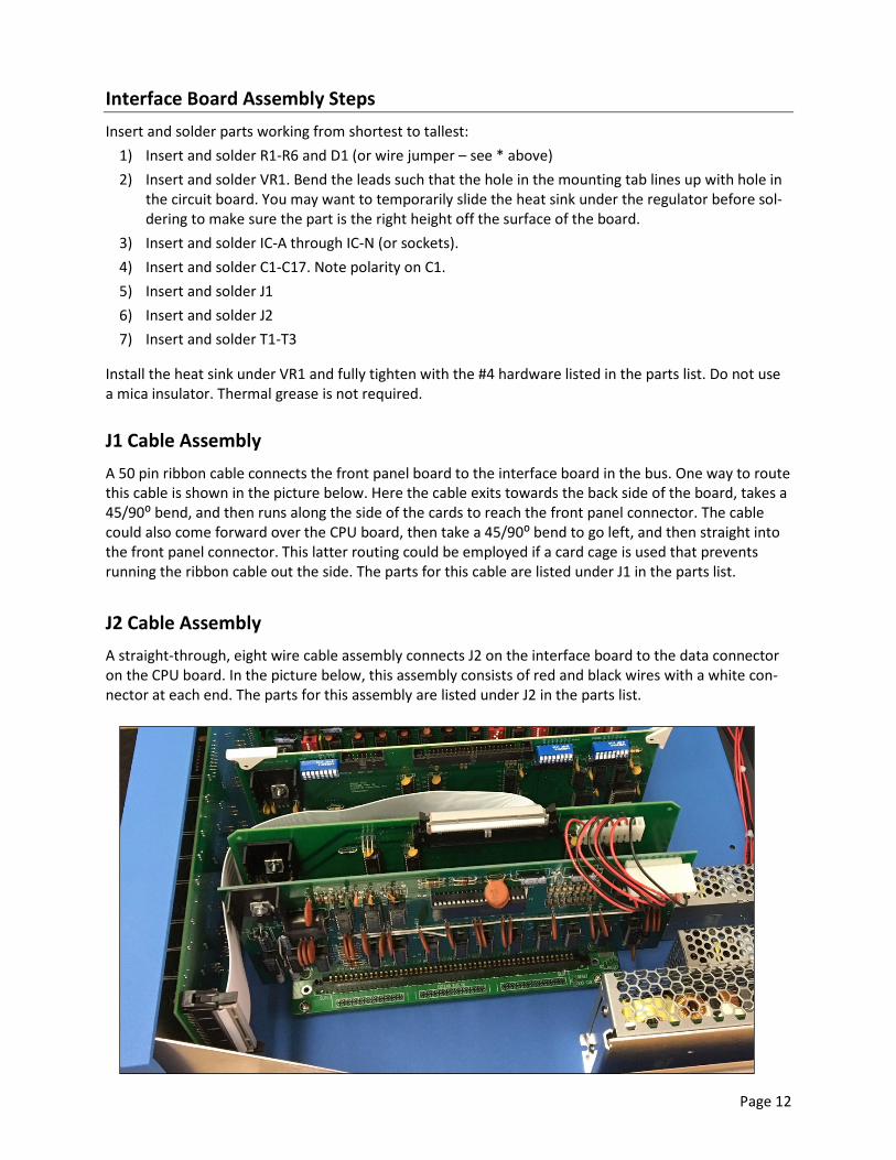
A 50 pin ribbon cable connects the front panel board to the interface board in the bus. One way to route
this cable is shown in the picture below. Here the cable exits towards the back side of the board, takes a
45/90⁰ bend, and then runs along the side of the cards to reach the front panel connector. The cable
could also come forward over the CPU board, then take a 45/90⁰ bend to go left, and then straight into
the front panel connector. This latter routing could be employed if a card cage is used that prevents
running the ribbon cable out the side. The parts for this cable are listed under J1 in the parts list.
J2 Cable Assembly
A straight-through, eight wire cable assembly connects J2 on the interface board to the data connector
on the CPU board. In the picture below, this assembly consists of red and black wires with a white con-
nector at each end. The parts for this assembly are listed under J2 in the parts list.
Page 13
Altair 8800c Computer Assembly Hints
Grounding
For maximum resistance to static shock, make sure all sections of the metal cabinet are in electrical con-
tact with each and with the power supply enclosures. Then also ensure the power cord ground wire is
connected to the chassis ground terminal on each of the power supplies.
As shipped, the Altair Clone case has lock washers that bite through the paint where the front panel
bracket attaches to the bottom pan and where the rear panel attaches to the bottom pan. This provides
an electrical connection between these pieces. If you drill holes and use screws to mount the power
supplies, the power supply chassis will most likely have good electrical contact with the bottom case
pan. If not, use lockwashers under the power supply mounting screws.
Unless connected elsewhere, connect the DC terminal used for signal ground to the chassis ground ter-
minal on at least one power supply. This ensures DC ground is at the same potential as chassis ground.
Motherboards with plated mounting holes that are connected to DC ground may make this connection
to chassis ground for you as well.
If putting screws through pre-drilled holes in the cabinet, paint may prevent electrical contact with the
screw. You can slightly ream the holes or use a lockwasher to bite through the paint to ensure electrical
connection to the bottom case pan.
Power Supply Note
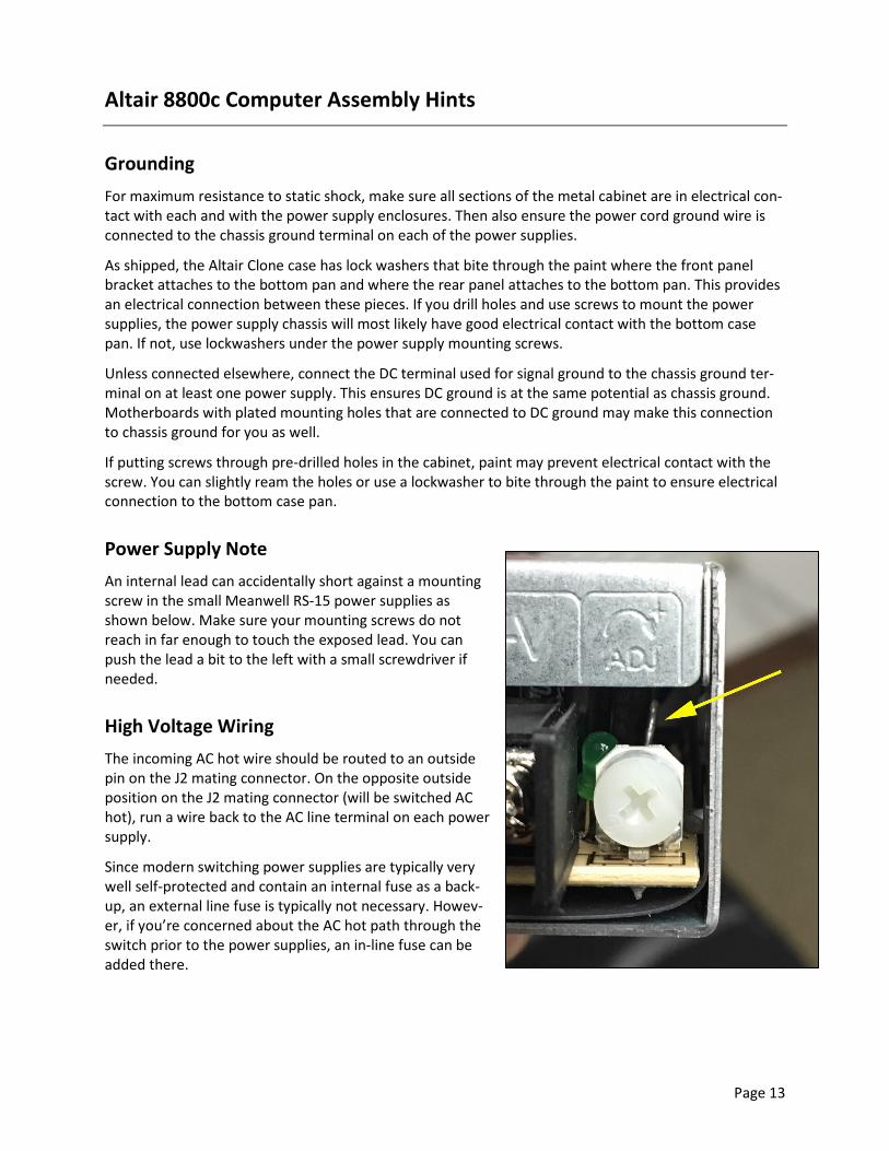
An internal lead can accidentally short against a mounting
screw in the small Meanwell RS-15 power supplies as
shown below. Make sure your mounting screws do not
reach in far enough to touch the exposed lead. You can
push the lead a bit to the left with a small screwdriver if
needed.
High Voltage Wiring
The incoming AC hot wire should be routed to an outside
pin on the J2 mating connector. On the opposite outside
position on the J2 mating connector (will be switched AC
hot), run a wire back to the AC line terminal on each power
supply.
Since modern switching power supplies are typically very
well self-protected and contain an internal fuse as a back-
up, an external line fuse is typically not necessary. Howev-
er, if you’re concerned about the AC hot path through the
switch prior to the power supplies, an in-line fuse can be
added there.
Page 14
Front Panel Operation
In its default configuration, the 8800c Front Panel board set duplicates the operation of the original Al-
tair front panel. In addition, the following features can be selectively enabled as desired:
• Power-on to a valid reset state
• An output latch at I/O address 0FFh that can display on the data LEDs
• Auto repeat single-step at selectable rate from 1hz-8hz, similar to the 8800b
• Code snippet injection: Common Altair bootstrap loaders, port echo routines, Kill-the-Bit, etc.
can be injected into RAM by selecting the desired code snippet on the lower eight address
switches, then depressing the AUX-Left switch.
• Auto jump on power-on (can be independent of reset operation)
• Auto jump on reset (can be independent of power-on operation)
These features are configured using three 8-bit “virtual” DIP switches (VDIPs). The following paragraphs
define the VDIP settings for each option. The process of setting the value of the virtual DIP switches is
covered in the “Updating Virtual DIP Switches” section further down in this manual.
7 6 5 4 3 2 1 0
VDIP #1 Pwr Reset FF Latch Code Inj ---- ---- Auto-Steps/sec (zero disables)
VDIP #2 MSB of Power-On Jump Address (zero disables)
VDIP #3 MSB of Reset Jump Address (zero disables)
Power-On Reset
By default, and to behave like the original Altair 8800 front panel, the run state of the 8800c Front Panel
is indeterminate at power-on and the 8080 is not given a RESET. This, in turn, tends to leave the 8080
processor in an invalid state as well. This is the reason for the manual STOP/RESET that must be per-
formed on the Altair front panel after power on.
To get around this problem, the 8800c Front Panel can be configured to automatically perform a
STOP/RESET during power-up. To enable this feature, set bit 7 of VDIP #1 to 1. To disable automatic re-
set, set the bit to 0.
Output Latch at 0FFh
An output latch can be enabled at I/O address 0FFh. The latch content can be displayed on the eight da-
ta LEDs on the front panel. The AUX-Right switch is used to choose between displaying the output latch
or normal output on the data LEDs.
While the computer is running, pressing the AUX-Right switch down displays the output latch on the da-
ta LEDs. Conversely, raising the AUX-Right switch restores normal display on the data LEDs.
Behavior while the computer is stopped is slightly different. When stopped, the normal LED display is
important for virtually every operation performed. Therefore normal data is automatically shown when-
Page 15
ever the computer is stopped. The output latch is displayed only while the AUX-Right switch is held
down – normal display is restored as soon as the switch is released.
The output latch feature is controlled by VDIP #1, bit 6. A value of 1 turns on the output latch, a value of
0 turns off the output latch.
Auto-Repeat Single Step
The 8800b provides an auto-repeat single step feature when the SINGLE-STEP switch is held down. This
same feature can be enabled on the 8800c Front Panel board. The lower three bits of VDIP #1 specify
the approximate auto-repeat rate in steps per second. A value of zero disables the auto-repeat feature.
Code Snippet Injection
A number of code snippets can be injected into RAM by entering the octal identifier for the desired code
snippet on switches A7-A0 (see below) and then depressing AUX-Left. After injection, an “examine” of
the start address is automatically performed, so simply depressing run starts the loaded code.
The code injection feature is enabled by VDIP #1, bit 5. A value of 1 enables code injection, a value of 0
disables code injection.
Bootstrap Loaders for BASIC
BASIC 1.0
000 2SIO
002 SIO
003 ACR
4K BASIC 3.2
004 2SIO
006 SIO
007 ACR
8K BASIC 3.2
010 2SIO
012 SIO
013 ACR
4K BASIC 4.0
014 2SIO
016 SIO
017 ACR
8K BASIC 4.0
020 2SIO
022 SIO
023 ACR
Extended BASIC 4.0
024 2SIO
026 SIO
027 ACR
Other Routines
ACR Leader Detector
030 For BASIC 3.2
031 For BASIC 4.0
Port Echo Routines
034 2SIO (1st port)
035 2SIO (2nd port)
036 SIO
037 ACR (SIO at 6/7)
Miscellaneous
040 Kill the Bit
041 Pong
044* Intel Hex Loader 2SIO (1st port)
045* Intel Hex Loader 2SIO (2nd port)
046 Memory Test (2SIO console)
*Relocatable – Set switches A15-A8 to the MSB of the desired load address before depressing AUX-Left

Page 16
Bootstrap Loaders
The BASIC Version 3.2 and 4.0 bootstrap loaders are straight from the Altair BASIC manuals. Refer to the
appropriate BASIC manual for how to load these versions of BASIC.
The Version 1.0 bootstrap loader runs at 1800h (014000 octal). Once BASIC is loaded, STOP/RESET the
machine and then depress RUN to get the startup dialog.
ACR Leader Detector
This is the code from the 88-ACR manual that looks for a valid leader byte before jumping to the boot-
strap loader. To use the leader detector, first inject the required bootstrap loader, then inject and run
the appropriate leader detector. As you’ll notice, the leader detector loads and runs at 100h (400 octal).
Kill the Bit
Kill the Bit game by Dean McDaniel, May 15, 1975. Object: Kill the rotating bit. If you miss the lit bit, an-
other bit turns on leaving two bits to destroy. Quickly toggle the switch, don't leave the switch in the up
position. Before starting, make sure all the switches are in the down position.
See http://deramp.com/downloads/altair/software/miscellaneous/
Pong
PONG for Altair front panel. Left player quickly toggles A15 to hit the "ball." Right player toggles A8.
Score is kept in memory locations 80h and 81h (left and right). Score is missed balls, so the lower num-
ber wins.
See http://deramp.com/downloads/altair/software/miscellaneous/
Intel Hex Loader
Loads an Intel hex file through the chosen 2SIO serial port. The program is relocatable: Set switches A15-
A8 to the MSB of the desired load address before depressing AUX-Left. The program prompts the opera-
tor to send the hex file. Once the complete hex file is received, the program pauses in an endless loop.
At this point, STOP/RESET to regain front panel control.
Memory Test
At the "*" prompt, key in four hex characters for the starting address followed by four hex characters for
the ending address. Press ESC to restart entry if a mistake is made. The test begins immediately when
the last digit of the ending address is typed (RETURN not required).
The starting address is typically 0100h (the program is on page zero). If RAM ends at DFFF (for example),
specify an end address of E000. This will cause the program to print an "error" for E000 at the comple-
tion of each test cycle as an indicator of activity.
The test runs continuously until reset. The program generates a pseudo-random number sequence,
writes a portion of it into RAM, and then regenerates the sequence from the same point to compare
with what is read from memory. If the pass is correct, a new portion of the sequence is written to a new
section of memory and the process repeats. Errors are printed out with the address, what was written
followed by what was read.
Page 17
Power-On and Reset Auto-Jump
The front panel can force an auto-jump upon power-on and/or reset. The auto-jump address can be dif-
ferent for power-on than for reset. This is unlike many auto-jump circuits which perform the same ac-
tion for power-on and for reset. For Altair BASIC and Altair DOS, duplicate auto-jump addresses can be
problematic. For example, the RESET switch is normally used to regain control from an executing or
hung program and return to the BASIC or DOS prompt. However, if the RESET switch instead forces an
auto-jump to the cold boot code in PROM, then the entire initialization process for BASIC or DOS – in-
cluding the slow process of mounting each disk – must be performed. For these programs, it is best to
have a power-on auto-jump without a reset auto-jump.
Power-On Auto-Jump
The MSB of the power-on auto-jump address is specified on VDIP #2. If a non-zero value is specified,
then upon power-on, the front panel forces a clean reset, an “examine” of the auto-jump address, and
then lets the 8080 processor run. If a value of zero is specified, power-on auto-jump is disabled.
Reset Auto-Jump
Whenever RESET is released, the front panel can force an “examine” of an address you specify. This sets
the 8080 program counter to this address and therefore performs an auto-jump to the specified address
if the computer is running. Note that if the computer is not running when RESET is actuated (or a
STOP/RESET is performed), this has the effect of examining the auto-jump address upon reset with the
computer remaining in a stopped state.
The MSB of the reset auto-jump address is specified on VDIP #3. If a value of zero is specified, the reset
auto-jump is disabled.
Updating Virtual DIP Switches
The virtual DIP switch (VDIP) values are stored in EEPROM. The VDIP values can be examined and updat-
ed from the front panel. The AUX-Right switch is used like the “Ctrl” key on a keyboard to give each
front panel switch an additional function. While holding AUX-Right in the UP position, the front panel
switches provide the following functions when actuated:
EXAMINE (with AUX-Right held up) places the value of VDIPs 1-3 into Altair RAM locations 1-3. The
firmware version is placed into RAM location zero. This allows you to “examine” the virtual DIP
switch values.
DEPOSIT (with AUX-Right held up) “deposits” the values from Altair memory locations 1-3 into VDIPs
1-3 in EEPROM.
RESET (with AUX-Right held up) resets the front panel into safe mode. See the “Firmware Updates”
section for more information about safe mode.
Once VDIP values are placed into Altair RAM using AUX-Right/EXAMINE, the values can be viewed and
changed in Altair memory using normal front panel examine and deposit operations. Once the VDIP val-
ues are as you want them, write them back to EEPROM using the AUX-Right/DEPOSIT sequence.
Page 18
Firmware Updates
The logic on the front panel and interface boards is controlled by a state machine in a PIC16F1828 pro-
cessor. The firmware in the processor can be updated while the board set is installed in a working Altair
computer. The computer must have at least 8K of RAM and a functional 2SIO port at the standard I/O
address (10h/11h).
To update firmware, the front panel must be placed into “safe mode” by holding the AUX-Right switch in
the UP position while powering on the Altair computer. Safe mode is a fully functional version of the
firmware in a protected area of flash memory. Safe mode provides all the functions of the original Altair
front panel and also the ability to program the “normal mode” area of flash memory. Safe mode does
not rely on parameters from EEPROM and provides none of the enhanced features available in the nor-
mal mode firmware. This allows safe mode to serve as a fail-safe backup to ensure front panel function-
ality even if the normal mode code is missing, corrupted, or has a fatal bug.
To update firmware, connect a PC running a terminal emulator to the 2SIO port in the Altair. The emula-
tor should be set for 8N1 with the baud rate determined by the 2SIO board. With the front panel already
in safe mode, raise and hold AUX-Right in the up position, then raise and release AUX-Left to start the
firmware update process. A prompt from the Altair should appear on the terminal emulator window.
Follow the prompt to send the .hex file that contains the firmware update from the PC. Once the .hex
file is received, the update is automatically programmed into flash and the front panel restarts into the
updated normal mode code.
When firmware is updated, the EEPROM containing the virtual DIP switch parameters is erased to zero.
You will need to re-configure the VDIP switches to match your feature preferences.
Helpful Hints
When the firmware update mode is entered, you should notice the WAIT light turn off (or go very dim)
since the Altair is now running a small program that was injected into memory by the front panel. If the
WAIT light stays bright, this indicates the 8080 is still stopped and the injected code failed to run. This is
typically because the front panel wasn’t actually in safe mode or there is a problem with RAM in the first
8K of address space.
If the Altair is running the injected program, but you don’t have terminal response, try typing a ctrl-c on
the terminal and see if an abort message appears. If not, perform a RESET on the front panel which re-
turns the front panel to normal operation, then attempt the AUX-Right/AUX-Left entry sequence again.
Additional Notes about Safe Mode and Normal Mode
Safe mode is entered in three conditions:
1) AUX-Right is held up when the computer is powered on
2) The normal mode area of flash is erased
3) While in normal mode, RESET is raised and released while AUX-Right is held up
Note that if normal mode is functional, safe mode can be entered from normal mode by performing
item #3 above.


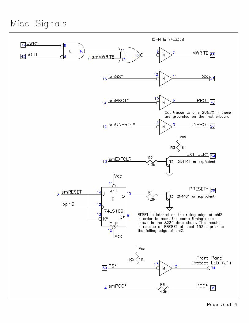
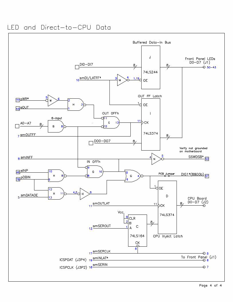
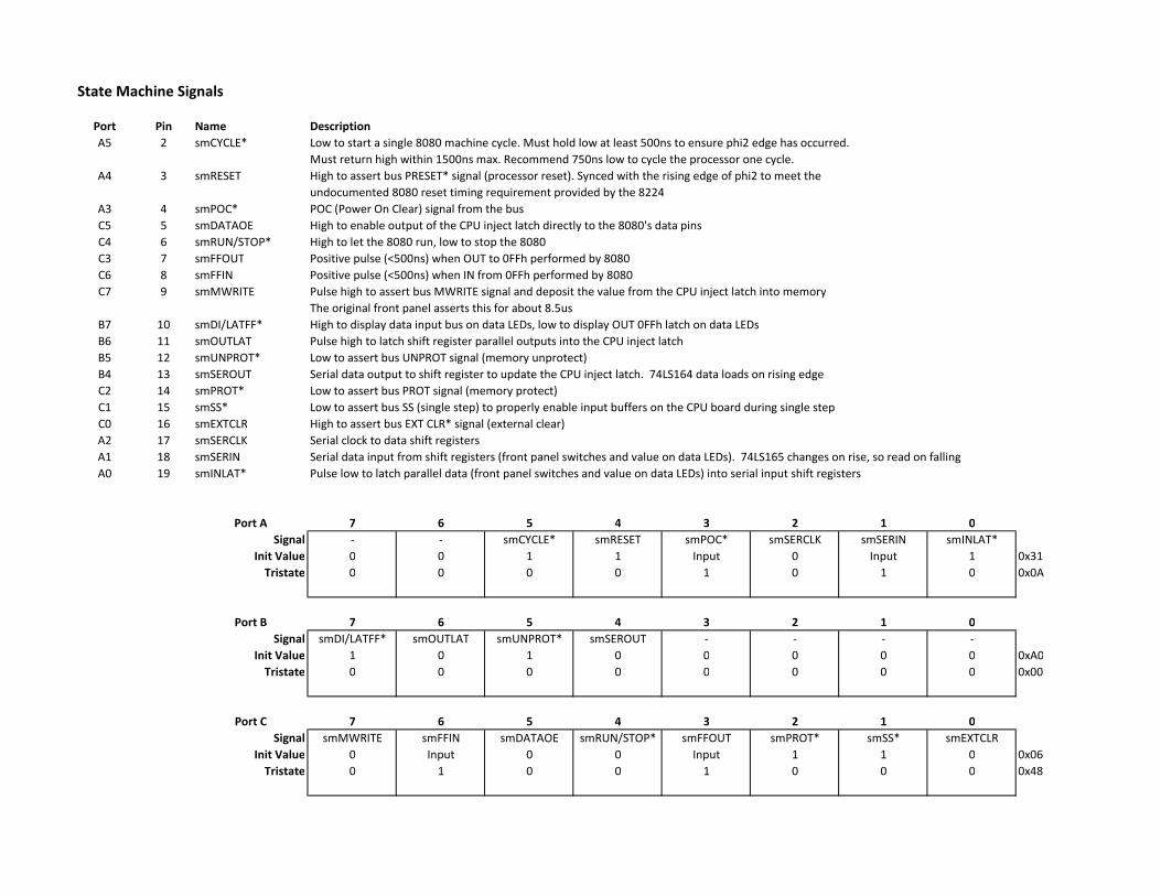
State Machine Signals
Port Pin Name Description
A5 2 smCYCLE* Low to start a single 8080 machine cycle. Must hold low at least 500ns to ensure phi2 edge has occurred.
Must return high within 1500ns max. Recommend 750ns low to cycle the processor one cycle.
A4 3 smRESET High to assert bus PRESET* signal (processor reset). Synced with the rising edge of phi2 to meet the
undocumented 8080 reset timing requirement provided by the 8224
A3 4 smPOC* POC (Power On Clear) signal from the bus
C5 5 smDATAOE High to enable output of the CPU inject latch directly to the 8080's data pins
C4 6 smRUN/STOP* High to let the 8080 run, low to stop the 8080
C3 7 smFFOUT Positive pulse (<500ns) when OUT to 0FFh performed by 8080
C6 8 smFFIN Positive pulse (<500ns) when IN from 0FFh performed by 8080
C7 9 smMWRITE Pulse high to assert bus MWRITE signal and deposit the value from the CPU inject latch into memory
The original front panel asserts this for about 8.5us
B7 10 smDI/LATFF* High to display data input bus on data LEDs, low to display OUT 0FFh latch on data LEDs
B6 11 smOUTLAT Pulse high to latch shift register parallel outputs into the CPU inject latch
B5 12 smUNPROT* Low to assert bus UNPROT signal (memory unprotect)
B4 13 smSEROUT Serial data output to shift register to update the CPU inject latch. 74LS164 data loads on rising edge
C2 14 smPROT* Low to assert bus PROT signal (memory protect)
C1 15 smSS* Low to assert bus SS (single step) to properly enable input buffers on the CPU board during single step
C0 16 smEXTCLR High to assert bus EXT CLR* signal (external clear)
A2 17 smSERCLK Serial clock to data shift registers
A1 18 smSERIN Serial data input from shift registers (front panel switches and value on data LEDs). 74LS165 changes on rise, so read on falling
A0 19 smINLAT* Pulse low to latch parallel data (front panel switches and value on data LEDs) into serial input shift registers
Port A 7 6 5 4 3 2 1 0
Signal - - smCYCLE* smRESET smPOC* smSERCLK smSERIN smINLAT*
Init Value 0 0 1 1 Input 0 Input 1 0x31
Tristate 0 0 0 0 1 0 1 0 0x0A
Port B 7 6 5 4 3 2 1 0
Signal smDI/LATFF* smOUTLAT smUNPROT* smSEROUT - - - -
Init Value 1 0 1 0 0 0 0 0 0xA0
Tristate 0 0 0 0 0 0 0 0 0x00
Port C 7 6 5 4 3 2 1 0
Signal smMWRITE smFFIN smDATAOE smRUN/STOP* smFFOUT smPROT* smSS* smEXTCLR
Init Value 0 Input 0 0 Input 1 1 0 0x06
Tristate 0 1 0 0 1 0 0 0 0x48

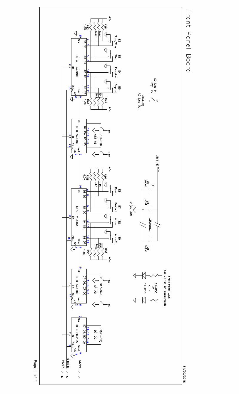
50 Pin Ribbon Cable to Front Panel
Pin Signal Pin Signal
1 +5v 2 +5v
3 +5v 4 +5v
5 SERCLK 6 INLAT
7 SERIN 8 N/C
9 N/C 10 WAIT
11 HLDA 12 A15
13 A14 14 A13
15 A12 16 A11
17 A10 18 A9
19 A8 20 A7
21 A6 22 A5
23 A4 24 A3
25 A2 26 A1
27 A0 28 N/C
29 Gnd 30 Gnd
31 Gnd 32 Gnd
33 INTE 34 PROT
35 MEMR 36 INP
37 M1 38 OUT
39 HLTA 40 STACK
41 WO 42 INT
43 D7 44 D6
45 D5 46 D4
47 D3 48 D2
49 D1 50 D0

IC Utilization
Front Panel Interface
Gates IC's Designator
74LS02 Quad 2-Input NOR 7 2 L,G 3/4 of G used
74LS00 Quad 2-Input NAND 4 1 H
74LS10 Triple 3-Input NAND 1 1 K 1/3 of K used
74LS30 Single 8-Input NAND 1 1 B
74LS04 Hex Inverter 5 1 M 5/6 of M used
74LS368 Hex Bus Driver 6 1 N
74LS109 Dual J-K* Flip Flop 4 2 E, F
74LS374 Octal Latch 2 2 D, I
74LS244 Octal Bus Driver 1 1 J
74LS164 Parallel Out Shift Register 1 1 C
PIC16F1828 Processor 1 1 A
Chip Count 14
Front Panel
74LS165 Parallel Load Shift Register 5 5 A-E

Altair Bus Signals
Pin Signal Description Pin Signal Description
1 +8v 51 +8v
2 +18v 52 -18v
3 XRDY Another RDY signal OR'd to 8080 53 SSWDSB* Direct sense switch input to the processor
4 VI0* Vectored interrupts 0-7 54 EXTCLR* Return all slave boards to known state
5 VI1* 55 RTC 60hz for Real-Time Clock
6 VI2* 56 STSTB* Status strobe
7 VI3* 57 DIG1 Data input gate 1 (for 8800b front panel)
8 VI4* 58 FRDY 8800b Front panel RDY to 8080
9 VI5* 59
10 VI6* 60
11 VI7* 61
12 62
13 63
14 64
15 65
16 66
17 67 PHANT* Not used in Altair
18 SDSB* Status disable (sMEMR, sWO, sM1, sINP, sOUT, sHLTA) 68 MWRT Memory Write (pWR* asserted and not SOUT)
19 CDSB* Control disable (pSYNC, pSTVAL, pDBIN, pWR, pHLDA) 69 PS* Memory protect status (out from addressed card)
20 UNPROT Front panel memory unprotect operation 70 PROT Front panel memory protect operation
21 SS Front panel single-step 71 RUN Machine is in the RUN state
22 ADSB* Address bus disable (A15-A0) 72 pRDY RDY signal OR'd with others to 8080
23 DODSB* Data Out bus disable (DO7-DO0) 73 pINT* Interrupt request to 8080
24 PHI2 Phase 2 clock 74 pHOLD* Hold request to 8080
25 PHI1 Phase 1 clock 75 pRESET* Reset line from from front panel reset switch
26 pHLDA 8080 hold acknowledge output 76 pSYNC 8080 start of machine cycle
27 pWAIT 8080 wait acknowledge output 77 pWR* 8080 write data valid
28 pINTE Asserted when the 8080 has interrupts enabled 78 pDBIN 8080 reading data bus
29 A5 79 A0
30 A4 80 A1
31 A3 81 A2
32 A15 82 A6
33 A12 83 A7
34 A9 84 A8
35 DO1 85 A13
36 DO0 86 A14
37 A10 87 A11
38 DO4 88 DO2
39 DO5 89 DO3
40 DO6 90 DO7
41 DI2 91 DI4
42 DI3 92 DI5
43 DI7 93 DI6
44 sM1 Machine cycle #1 (instruction fetch) 94 DI1
45 sOUT Write cycle for an OUT instruction taking place 95 DI0
46 sINP Read cycle for an IN instruction taking place 96 sINTA Bus cycle is interrupt acknowledge
47 sMEMR Read cycle is a memory read 97 sWO* Bus cycle is a write (memory or I/O)
48 sHLTA 8080 halt acknowledge output 98 sSTACK Bus cycle is a stack operation
49 CLOCK* 99 POC* Power on clear
50 GND 100 GND
Ground in IEEE-696 bus spec
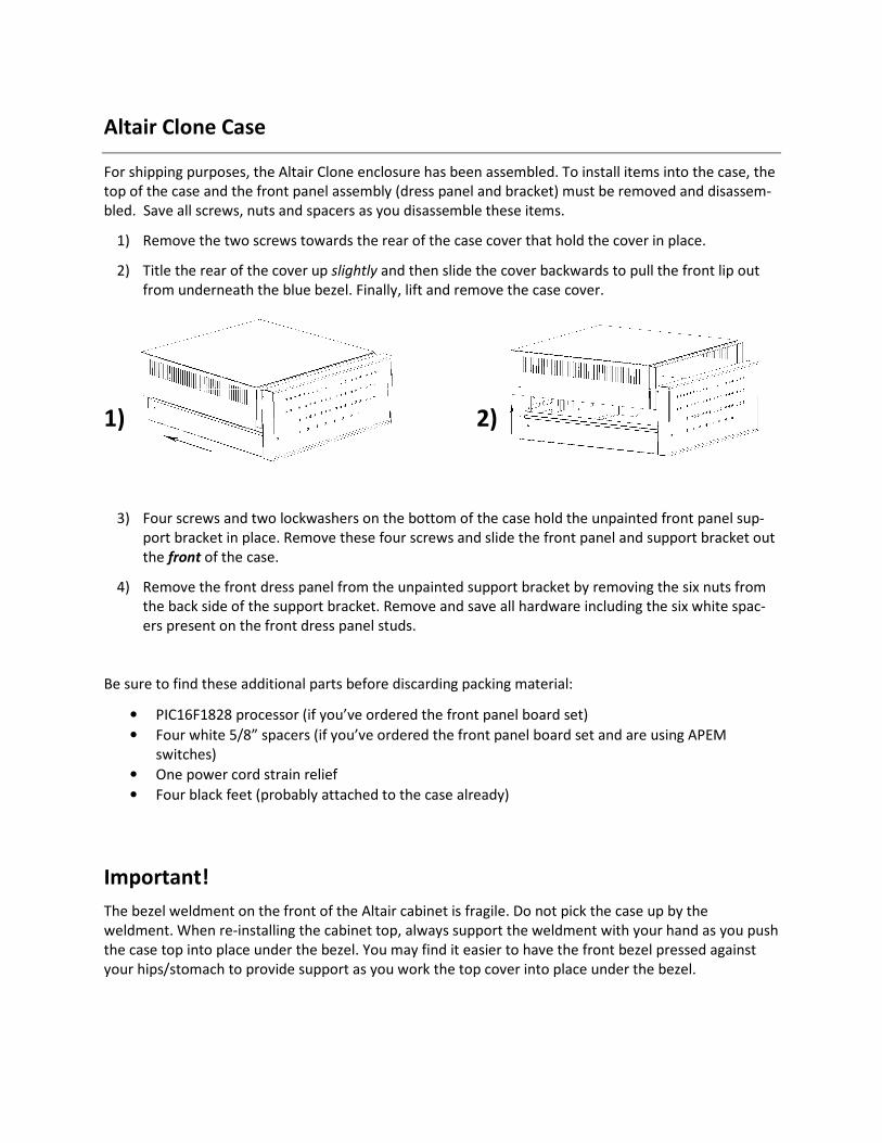
Altair Clone Case
For shipping purposes, the Altair Clone enclosure has been assembled. To install items into the case, the
top of the case and the front panel assembly (dress panel and bracket) must be removed and disassem-
bled. Save all screws, nuts and spacers as you disassemble these items.
1) Remove the two screws towards the rear of the case cover that hold the cover in place.
2) Title the rear of the cover up slightly and then slide the cover backwards to pull the front lip out
from underneath the blue bezel. Finally, lift and remove the case cover.
1)
2)
3) Four screws and two lockwashers on the bottom of the case hold the unpainted front panel sup-
port bracket in place. Remove these four screws and slide the front panel and support bracket out
the front of the case.
4) Remove the front dress panel from the unpainted support bracket by removing the six nuts from
the back side of the support bracket. Remove and save all hardware including the six white spac-
ers present on the front dress panel studs.
Be sure to find these additional parts before discarding packing material:
• PIC16F1828 processor (if you’ve ordered the front panel board set)
• Four white 5/8” spacers (if you’ve ordered the front panel board set and are using APEM
switches)
• One power cord strain relief
• Four black feet (probably attached to the case already)
Important!
The bezel weldment on the front of the Altair cabinet is fragile. Do not pick the case up by the
weldment. When re-installing the cabinet top, always support the weldment with your hand as you push
the case top into place under the bezel. You may find it easier to have the front bezel pressed against
your hips/stomach to provide support as you work the top cover into place under the bezel.