Embed Size (px)
Citation preview
Alessandra Pipino – XXIX cycle
Email: [email protected]; [email protected]
Midterm Seminar Day - 31st March 2015
System-level and circuital design of receivers for wireless communication
applications
Tutor: Prof. A. Baschirotto
A. PIPINO - Midterm Seminar Day 2
Outline• BLE System Design
• RF Filtering ADC
• Courses attended
31/03/2015
A. PIPINO - Midterm Seminar Day 3
Outline• BLE System Design
• RF Filtering ADC
• Course attended
31/03/2015
A. PIPINO - Midterm Seminar Day 4
BLE Standard• Purpose of the activity :
• Dimensioning of a receiver front-end compliant with the Bluetooth Low Energy standard communication
• In collaboration with :• Department of Electrical & Computer Engineering of
University of Toronto
• Hong Kong Applied Science and Technology Research Institute (ASTRI)
31/03/2015
A. PIPINO - Midterm Seminar Day 5
BLE Standard• Bluetooth Low Energy (BLE) is a new release of the
conventional Bluetooth• Lower power implementation long battery life• Lower complexity• Lower cost
• Applications:• Automotive• Mobile phones• Healthcare• Security & proximity
31/03/2015
A. PIPINO - Midterm Seminar Day 6
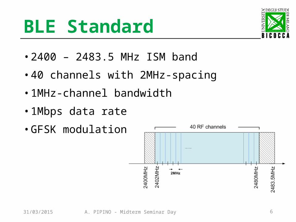
BLE Standard• 2400 – 2483.5 MHz ISM band
• 40 channels with 2MHz-spacing
• 1MHz-channel bandwidth
• 1Mbps data rate
• GFSK modulation
31/03/2015
A. PIPINO - Midterm Seminar Day 7
BLE Standard• Two main sections in the standard document:
• MAC Layer : • communication protocol
• digital baseband
• Physical Layer: • channel bandwidth, operative scenario, power, etc.
• analog front-end
31/03/2015
A. PIPINO - Midterm Seminar Day 8
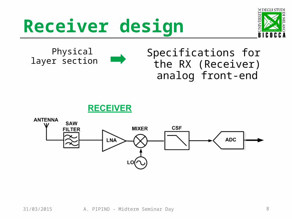
Receiver design Physical layer
sectionSpecifications for the RX
(Receiver) analog front-end
31/03/2015
A. PIPINO - Midterm Seminar Day 9
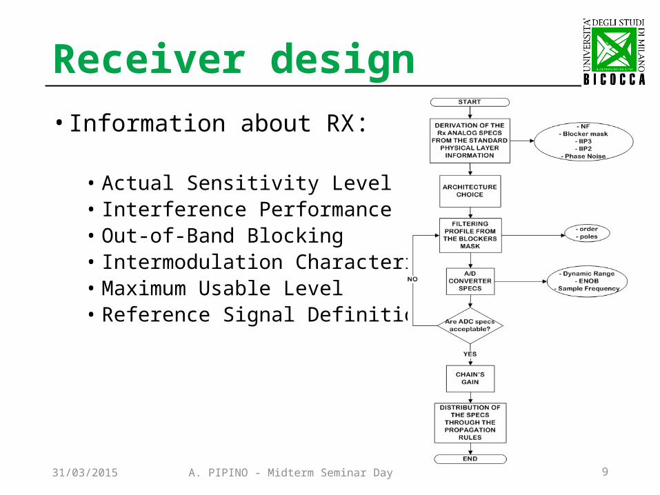
Receiver design• Information about RX:
• Actual Sensitivity Level• Interference Performance• Out-of-Band Blocking• Intermodulation Characteristics• Maximum Usable Level• Reference Signal Definition
31/03/2015
A. PIPINO - Midterm Seminar Day 10
Receiver design
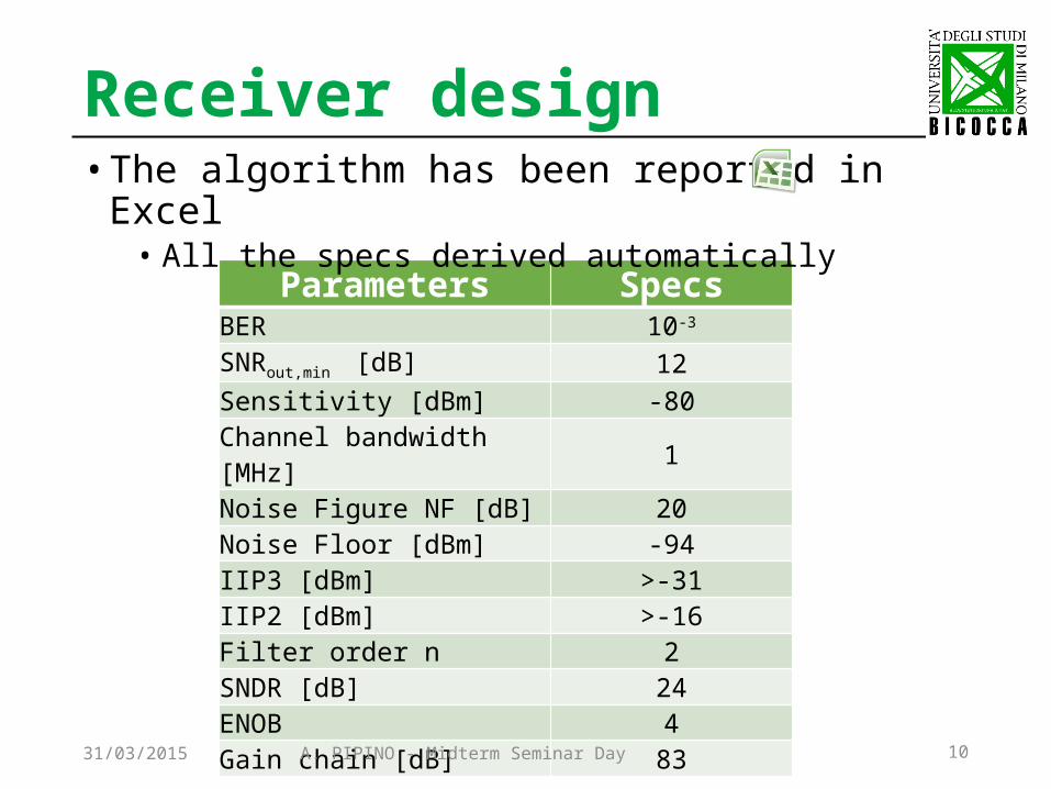
Parameters SpecsBER 10-3
SNRout,min [dB] 12Sensitivity [dBm] -80Channel bandwidth [MHz] 1Noise Figure NF [dB] 20Noise Floor [dBm] -94IIP3 [dBm] >-31IIP2 [dBm] >-16Filter order n 2SNDR [dB] 24ENOB 4Gain chain [dB] 83
• The algorithm has been reported in Excel• All the specs derived automatically
31/03/2015
A. PIPINO - Midterm Seminar Day 11
Receiver design
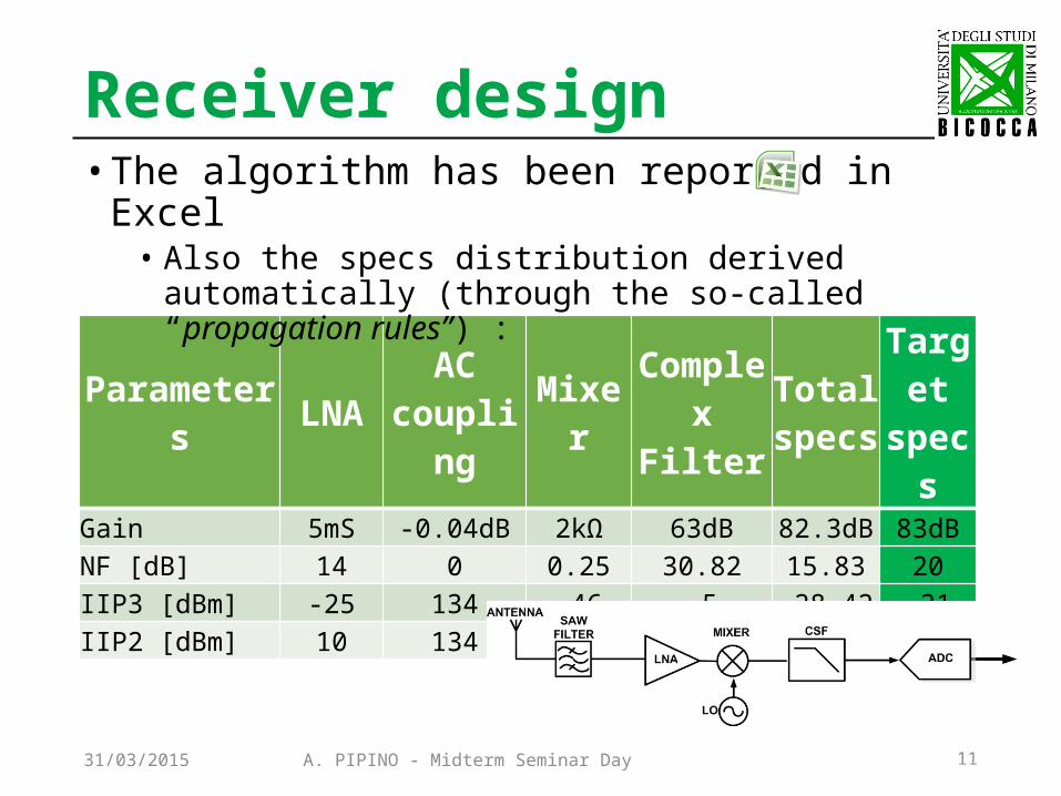
Parameters LNA AC coupling Mixer Complex
FilterTotal specs
Target specs
Gain 5mS -0.04dB 2kΩ 63dB 82.3dB 83dBNF [dB] 14 0 0.25 30.82 15.83 20IIP3 [dBm] -25 134 -46 -5 -28.42 -31IIP2 [dBm] 10 134 24 20 0.34 -16
• The algorithm has been reported in Excel• Also the specs distribution derived automatically (through the
so-called “propagation rules”) :
31/03/2015
A. PIPINO - Midterm Seminar Day 12
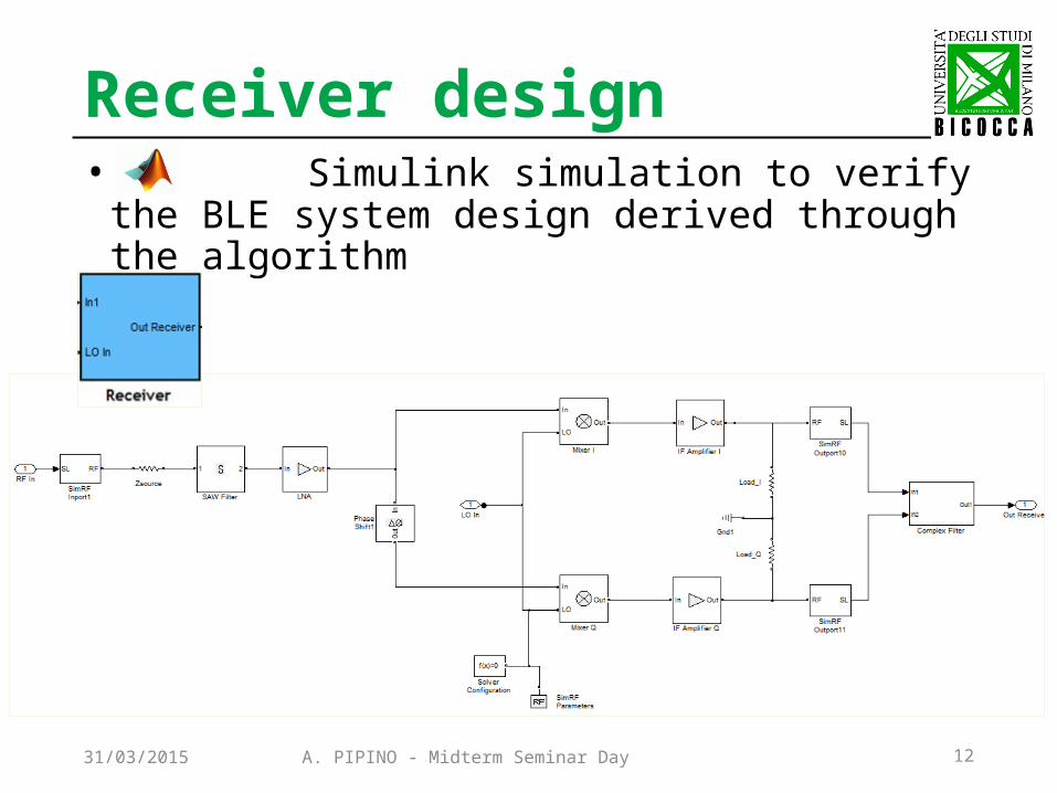
Receiver design• Simulink simulation to verify the BLE system
design derived through the algorithm
31/03/2015
A. PIPINO - Midterm Seminar Day 13
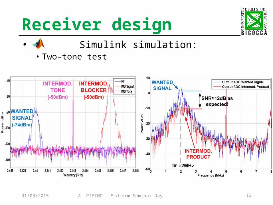
Receiver design• Simulink simulation:
• Two-tone test
31/03/2015
A. PIPINO - Midterm Seminar Day 14
Papers• A paper entitled “Bluetooth Low Energy Receiver Design”
submitted and accepted as lecture presentation at 2015 IEEE International Symposium on Circuits and Systems (ISCAS) (24-27May 2015, Lisbon-Portugal)
• A paper entitled “A Simple Link Budget Computation for Wireless Receivers” submitted for publication on Journal on Circuits, Systems and Computers (JCSC)
31/03/2015
A. PIPINO - Midterm Seminar Day 15
Outline• BLE Standard
• RF Filtering ADC
• Courses attended
31/03/2015
A. PIPINO - Midterm Seminar Day 16
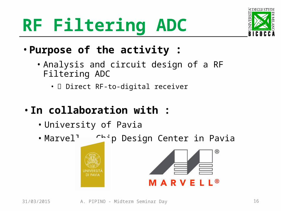
RF Filtering ADC• Purpose of the activity :
• Analysis and circuit design of a RF Filtering ADC• Direct RF-to-digital receiver
• In collaboration with :• University of Pavia
• Marvell – Chip Design Center in Pavia
31/03/2015
A. PIPINO - Midterm Seminar Day 17
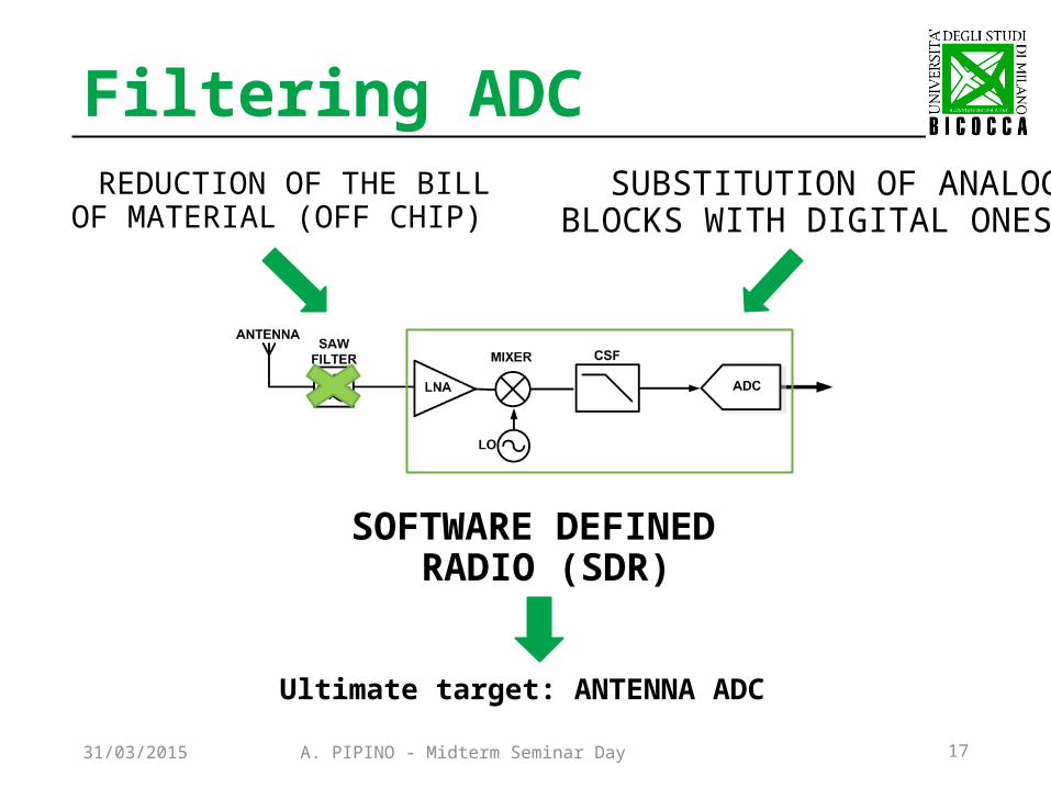
Filtering ADC REDUCTION OF THE BILL OF
MATERIAL (OFF CHIP) SUBSTITUTION OF ANALOG
BLOCKS WITH DIGITAL ONES
SOFTWARE DEFINED RADIO (SDR)
Ultimate target: ANTENNA ADC31/03/2015
A. PIPINO - Midterm Seminar Day 18
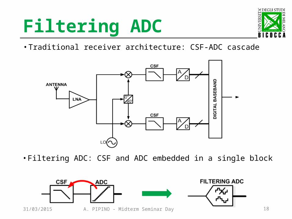
Filtering ADC• Traditional receiver architecture: CSF-ADC cascade
• Filtering ADC: CSF and ADC embedded in a single block
31/03/2015
A. PIPINO - Midterm Seminar Day 19
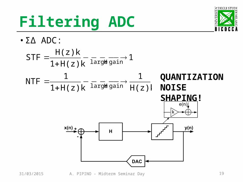
Filtering ADC• ΣΔ ADC:
31/03/2015
1H(z)k1
H(z)kSTF
gain H large
H(z)k
1
H(z)k1
1NTF
gain H large
QUANTIZATION
NOISE SHAPING!
A. PIPINO - Midterm Seminar Day 20
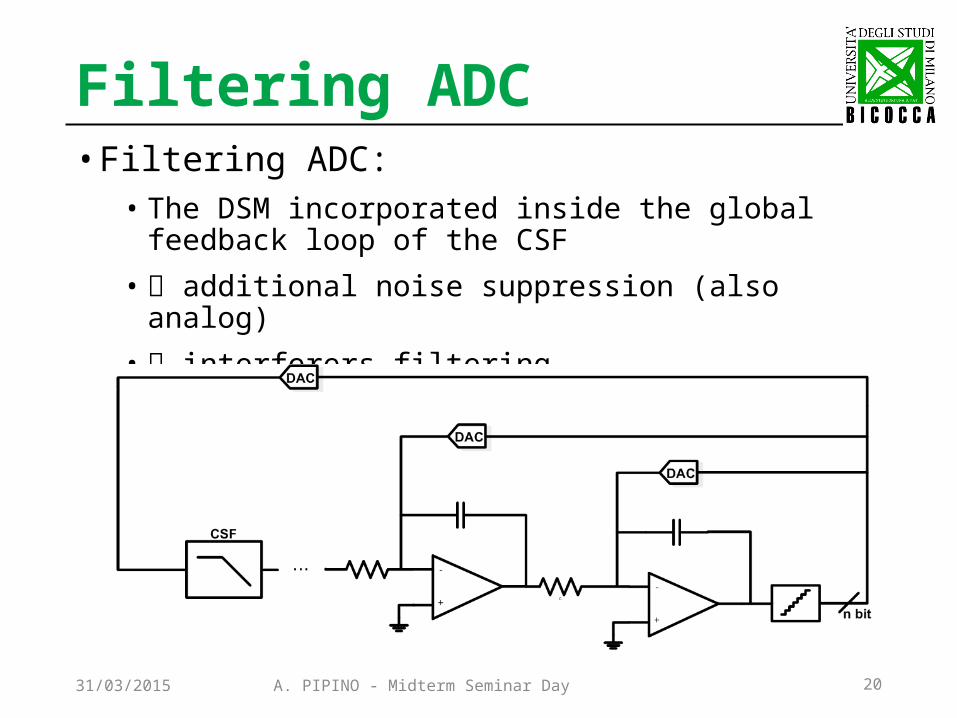
Filtering ADC• Filtering ADC:
• The DSM incorporated inside the global feedback loop of the CSF
• additional noise suppression (also analog)
• interferers filtering
31/03/2015
21
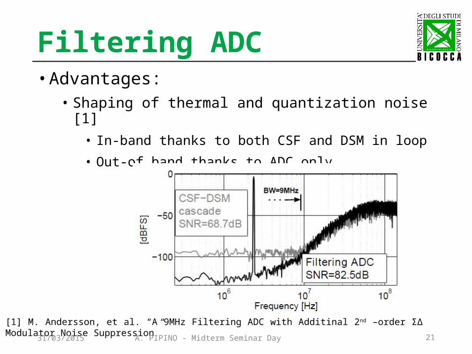
Filtering ADC• Advantages:
• Shaping of thermal and quantization noise [1]• In-band thanks to both CSF and DSM in loop
• Out-of band thanks to ADC only
[1] M. Andersson, et al. “A 9MHz Filtering ADC with Additinal 2nd –order ΣΔ Modulator Noise Suppression”
31/03/2015 A. PIPINO - Midterm Seminar Day
A. PIPINO - Midterm Seminar Day 22
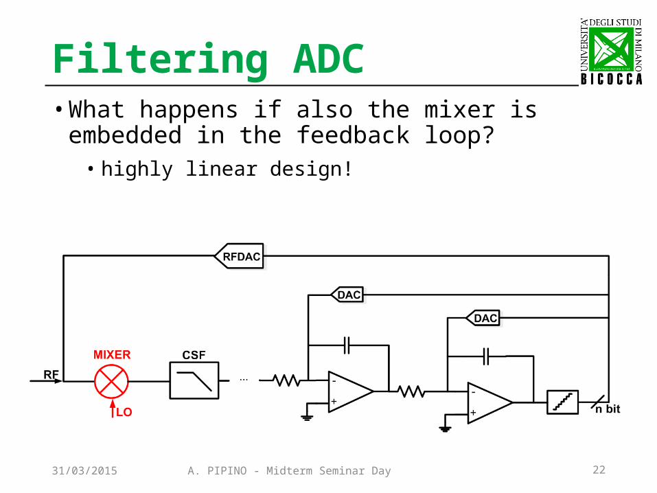
Filtering ADC• What happens if also the mixer is embedded in the
feedback loop?• highly linear design!
31/03/2015
A. PIPINO - Midterm Seminar Day 23
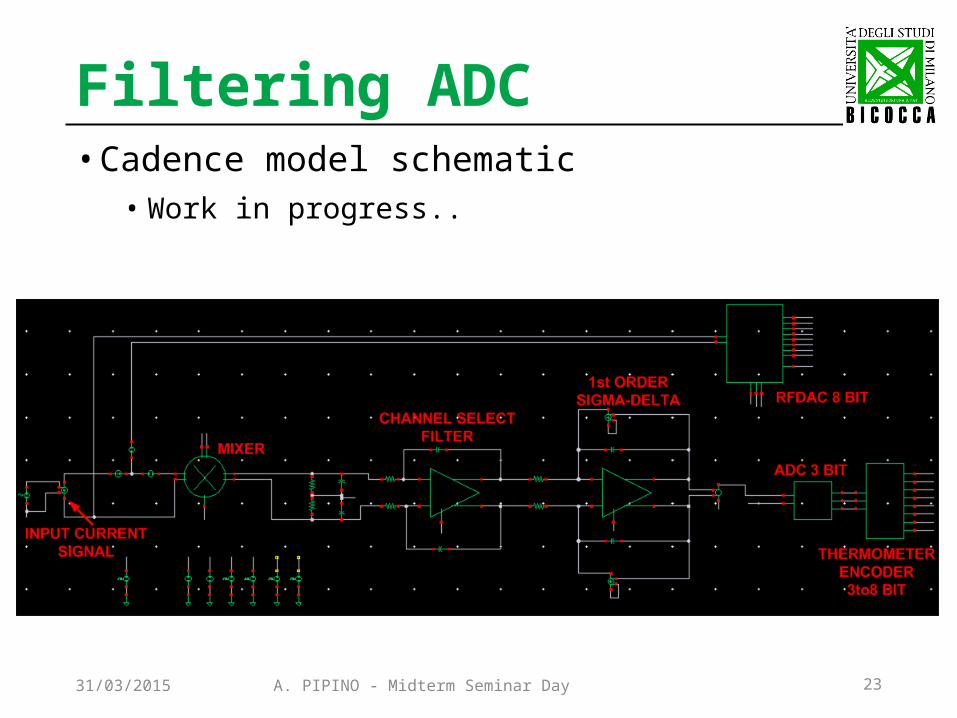
Filtering ADC• Cadence model schematic
• Work in progress..
31/03/2015
A. PIPINO - Midterm Seminar Day 24
Outline• BLE Standard
• RF Filtering ADC
• Courses attended
31/03/2015
A. PIPINO - Midterm Seminar Day 25
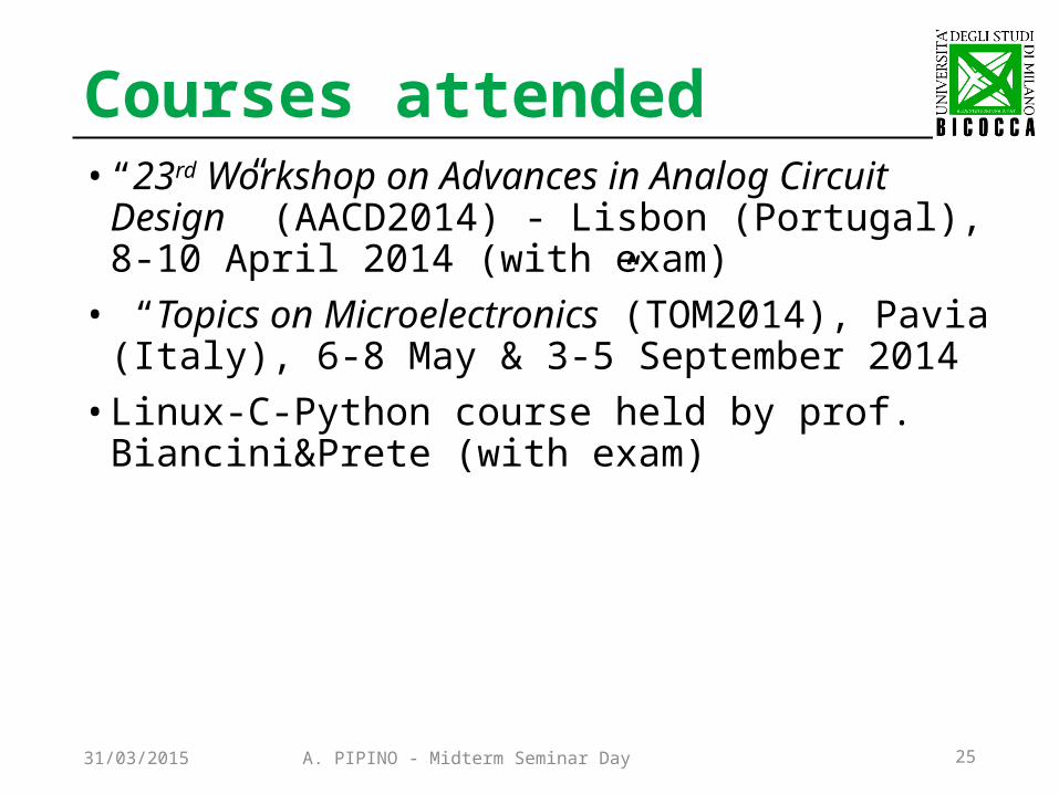
Courses attended• “23rd Workshop on Advances in Analog Circuit Design”
(AACD2014) - Lisbon (Portugal), 8-10 April 2014 (with exam)
• “Topics on Microelectronics”(TOM2014), Pavia (Italy), 6-8 May & 3-5 September 2014
• Linux-C-Python course held by prof. Biancini&Prete (with exam)
31/03/2015
A. PIPINO - Midterm Seminar Day 26
Thank you for your attention!
31/03/2015


![Design of Factorial Survey Experiments in Stata · Design of Factorial Survey Experiments in Stata Author: Maurizio Pisati and Livia Ridolfi [2pt] maurizio.pisati@unimib.it l.ridolfi@campus.unimib.it](https://img.dokumen.tips/doc/110x75/5b865c5a7f8b9a212e8bf846/design-of-factorial-survey-experiments-in-stata-design-of-factorial-survey-experiments.jpg)

![Pipino v. Norman - Supreme Court of Ohio[Cite as Pipino v.Norman, 2017-Ohio-9048.] ROBB, P.J. {¶1} This case presents an appeal and a purported cross-appeal. Gallagher Sharp (the](https://img.dokumen.tips/doc/110x75/60a7d09ba67a8e2c876932f5/pipino-v-norman-supreme-court-of-cite-as-pipino-vnorman-2017-ohio-9048-robb.jpg)