Embed Size (px)
Citation preview

Avance Logic,Inc. ALC100
ALC100/ALC100PAC’97 Audio CODEC
Revision 1.1
May 25, 2000

Avance Logic,Inc. ALC100
- 2 – Rev 1.1
1. Features :l Single chip audio CODEC with high S/N ratio.l 16-bit ADC and DAC resolution.l Compliant with AC’97 2.1 specificationl Supports AMR and CNR applications.l 16-bit stereo full-duplex CODEC with fixed 48k sampling rate.l 4 analog line-level stereo input with 5-bit volume control : LINE_IN,CD,VIDEO,AUXl 2 analog line-level mono input : PC_BEEP,PHONE_IN.l Mono output with 5-bit volume control.l Stereo output with 5-bit volume control.l 2 MIC inputs : Software selectable.l Power management.l 3D Stereo Enhancementl True Line-Level outputl Multiple CODEC extension.l External Amplifier power down capability.l Dual power support : Digital :5V/3.3V Analog : 5V`l Standard 48-Pin LQFP Package
2. Pin Description :2.1 Digital I/O pins : 11 pins
Name Type Pin No Description Characteristic DefinitionRESET# I 11 AC'97 master H/W reset CMOS input,Vt=0.35Vdd *XTL-IN I 2 Crystal input pad (24.576Mhz) Crystal input pad
XTL-OUT O 3 Crystal output pad Crystal output padSYNC I 10 Sample Sync (48Khz) CMOS input,Vt=0.35Vdd
BIT-CLK IO 6 Bit clock output (12.288Mhz) CMOS input/output Vt=0.35Vdd (Refer 6.2.5)*SDATA-OU
TI 5 Serial TDM AC97 output CMOS input,Vt=0.35Vdd
SDATA-IN O 8 Serial TDM AC97 input CMOS output (Refer 6.2.5)ID0# I 45 ID strap 0 CMOS input Vt=0.35Vdd with 50KΩ pull highID1# I 46 ID strap 1 CMOS input Vt=0.35Vdd with 50KΩ pull highEAPD O 47 External Amplifier power down
control8mA CMOS output
PWRI# I 48 Internal register reset (For test) CMOS input
2.2 Analog I/O Pins : 18 pinsName Type Pin No Description Characteristic Definition
PC-BEEP I 12 PC speaker input Analog input (1Vrms)PHONE I 13 speakerphone input Analog input (1Vrms)
AUX-L I 14 AUX Left channel Analog input (1Vrms)AUX-R I 15 AUX Right channel Analog input (1Vrms)
VIDEO-L I 16 Video audio Left channel Analog input (1Vrms)VIDEO-R I 17 Video audio Right channel Analog input (1Vrms)
CD-L I 18 CD audio Left channel Analog input (1Vrms)CD-GND I 19 CD audio analog GND Analog input (1Vrms)
CD-R I 20 CD audio Right channel Analog input (1Vrms)MIC1 I 21 First Mic input Analog input (1Vrms)MIC2 I 22 Second Mic input Analog input (1Vrms)
LINE-L I 23 Line input Left channel Analog input (1Vrms)LINE-R I 24 Line input Right channel Analog input (1Vrms)
LINE-OUTL O 35 Line-Out Left channel Analog output (1Vrms)LINE-OUTR O 36 Line-Out Right channel Analog output (1Vrms)
LNLVL-L O 39 True Line Level output-Left Analog output (1Vrms)LNLVL-R O 41 True Line Level output-Right Analog output (1Vrms)
MONO-OUT
O 37 SpeakerPhone output Analog output (1Vrms)
2.3 Filter/References : 11 pinsName Type Pin No Description Characteristic Definition
VREF O 27 Reference voltage Analog output (2.25~2.75V)

Avance Logic,Inc. ALC100
- 3 – Rev 1.1
VREFOUT O 28 Reference voltage out with 5mA drive
Analog output (2.25~2.75V)
DALO O 29 DA Left output filter Analog output DARO O 30 DA Right output filter Analog output
VRADDA O 31 VRADDA filter Analog output DALI O 32 DALI filter Analog output DALO O 33 DARI filter Analog output ADLO O 34 AD Left filter Analog output ADRO O 40 AD Right filter Analog output ADLI O 43 ADLI filter Analog outputADRI O 44 ADRI filter Analog output
2.4 Power/Ground : 8 pinsName Type Pin No Description Characteristic Definition
AVDD1 I 25 Analog VDD (5.0V)AVDD2 I 38 Analog VDD (5.0V)AVSS1 I 26 Analog GNDAVSS2 I 42 Analog GNDVDD1 I 1 Digital VDD (5.0V or 3.3V)VDD2 I 9 Digital VDD (5.0V or 3.3V)VSS1 I 4 Digital GNDVSS2 I 7 Digital GND
*When RESET# is active the BIT-CLK and SDATA-IN must be floating by internal pull low 100K resistors. So the ac-link signals are driven by another AC’97 on CNR board. This requirement is not mentioned in AC’97 specification rev2.1, please refer CNR (Communication Network Riser) specification rev1.0 page23~25 to get detail information.

Avance Logic,Inc. ALC100
- 4 – Rev 1.1
3. ALC100 Pin-Out Diagram :
LIN
E_IN
_R
LIN
E_IN
_L
MIC
2
MIC
1
CD
_R
CD
_GN
D
CD
_L
VID
EO_R
VID
EO_L
AU
X_R
AU
X_L
PHO
NE
PC_BEEP
RESET#
SYNC
DVdd2
SDATA_IN
DVss2
BIT_CLK
SDATA_OUT
DVss1
XTL_OUT
XTL_IN
DVdd1
MO
NO
_OU
T
AV
dd2
LNLV
L_O
UT_
L
AD
RO
LNLV
L_O
UT_
R
AV
ss2
AD
LI
AD
RI
ID0#
ID1#
EAPD
PWR
I#
AVdd1
AVss1
Vref
Vrefout
DALO
DARO
VRADDA
DALI
DARI
ADLO
LINE_OUT_L
LINE_OUT_R48 47 46 45 44 43 42 41 40 39 38 37
36
35
34
33
32
31
30
29
28
27
26
25
242322212019181716151413
12
11
10
9
8
7
6
5
4
3
2
1
ALC100/ALC100P
Pinout Diagram of ALC100/ALC100P

Avance Logic,Inc. ALC100
- 5 – Rev 1.1
4. Mixer Register :All mixer register access with odd-number will return with 0.Reading unimplemented registers will return 0.
MX00 Reset Default : 5800hBit Type Function15 Reserved
14:10 R return 16H9 R Read as 0 (No support 20-bit ADC)8 R Read as 0 (No support 18-bit ADC)7 R Read as 0 (No support 20-bit DAC)6 R Read as 0 (No support 18-bit DAC)5 R Read as 0 (No support for Loudness)4 R Read as 0 (No HeadPhone-Out support)3 R Read as 0 (No simulated stereo ,for analog 3D block use)2 R Read as 0 (No Bess & Treble Control)1 R Reserved,Read as 0 0 R Read as 0 (No Dedicated Mic PCM input)Write to this register will reset all mixer registe2r to their default value. The write data is
ignored.MX02 Master Volume Default : 8000h
Bit Type Function15 R/W Mute Control 0 : Normal 1 : Mute (-∞ dB)
14:13 Reserved12:8 R/W Master Left Volume (MLV[4..0]) in 1.5 dB step7:5 Reserved4:0 R/W Master Right Volume (MRV[4..0]) in 1.5 dB step
For MRV/MLV,00h 0 dB attenuation1Fh 46.5 dB attenuation
MRV/MLV are 5-bit R/W variables. The 6th bit implementation is optional. For this reason, when 6th bit is written by 1,it is equivalent to writing low 5-bit with 1. For example, writing 1xxxxx will read back 01111.
MX04 Line Level Output Volume Default : 8000hBit Type Function15 R/W Mute Control 0 : Normal 1 : Mute (-∞ dB)
14:13 Reserved12:8 R/W Line Level Output Left Volume (LNLV[4..0]) in 1.5 dB step7:5 Reserved4:0 R/W Line Level Output Right Volume (LNRV[4..0]) in 1.5 dB step
For LNRV/LNLV,00h 0 dB attenuation1Fh 46.5 dB attenuation
Implement 5-bit volume control only. Writing 1xxxxx will be interpreted as x11111 and response when read with x11111 too.
MX06 MONO_OUT Volume Default : 8000H Bit Type Function15 R/W Mute Control 0 : Normal 1 : Mute (-∞ dB)
14:5 Reserved4:0 R/W Mono Master Volume (MMV[4..0]) in 1.5 dB step
For MMV,00h 0 dB attenuation1Fh 46.5 dB attenuation
Implement 5-bit volume control only. Writing 1xxxxx will be interpreted as x11111 and

Avance Logic,Inc. ALC100
- 6 – Rev 1.1
response when read with x11111 too.MX0A PC BEEP Volume Default : 0000H
Bit Type Function15 R/W Mute Control 0 : Normal 1 : Mute (-∞ dB)
14:5 Reserved4:1 R/W PC Beep Volume (PBV[3..0]) in 3 dB step0 Reserved For PBV,
00h 0 dB attenuation0Fh 45 dB attenuation
MX0C PHONE Volume Default : 8008HBit Type Function15 R/W Mute Control 0 : Normal 1 : Mute (-∞ dB)
14:5 Reserved4:0 R/W Phone Volume (PV[4..0]) in 1.5 dB step
For PV,00h +12 dB Gain08h 0dB gain1Fh -34.5dB Gain
MX0E MIC Volume Default : 8008HBit Type Function15 R/W Mute Control 0 : Normal 1 : Mute (-∞ dB)
14:7 Reserved6 R/W 20 dB boost control 0 : Normal 1: 20 dB boost5 Reserved
4:0 R/W Mic Volume (MV[4..0]) in 1.5 dB step For MV,
00h +12 dB Gain08h 0dB gain1Fh -34.5dB Gain
MX10 LINE_IN Volume Default : 8808HBit Type Function15 R/W Mute Control 0 : Normal 1 : Mute (-∞ dB)
14:13 Reserved12:8 R/W Line-In Left Volume (NLV[4..0]) in 1.5 dB step7:5 Reserved4:0 R/W Line-In Right Volume (NRV[4..0]) in 1.5 dB step
For NLV/NRV,00h +12 dB Gain08h 0dB gain1Fh -34.5dB Gain
MX12 CD Volume Default : 8808H Bit Type Function15 R/W Mute Control 0 : Normal 1 : Mute (-∞ dB)
14:13 Reserved12:8 R/W CD Left Volume (CLV[4..0]) in 1.5 dB step7:5 Reserved4:0 R/W CD Right Volume (CRV[4..0]) in 1.5 dB step
For CLV/CRV,00h +12 dB Gain08h 0dB gain1Fh -34.5dB Gain
MX14 VIDEO Volume Default : 8808H Bit Type Function

Avance Logic,Inc. ALC100
- 7 – Rev 1.1
15 R/W Mute Control 0 : Normal 1 : Mute (-∞ dB)14:13 Reserved12:8 R/W Video Left Volume (VLV[4..0]) in 1.5 dB step7:5 Reserved4:0 R/W Video Right Volume (VRV[4..0]) in 1.5 dB step
For VLV/VRV,00h +12 dB Gain08h 0dB gain1Fh -34.5dB Gain
MX16 AUX Volume Default : 8808H Bit Type Function15 R/W Mute Control 0 : Normal 1 : Mute (-∞ dB)
14:13 Reserved12:8 R/W AUX Left Volume (ALV[4..0]) in 1.5 dB step7:5 Reserved4:0 R/W AUX Right Volume (ARV[4..0]) in 1.5 dB step
For ALV/ARV,00h +12 dB Gain08h 0dB gain1Fh -34.5dB Gain
MX18 PCM_OUT Volume Default 8808HBit Type Function15 R/W Mute Control 0 : Normal 1 : Mute (-∞ dB)
14:13 Reserved12:8 R/W PCM Volume (PLV[4..0]) in 1.5 dB step7:5 Reserved4:0 R/W PCM Right Volume (PRV[4..0]) in 1.5 dB step
For PLV/PRV,00h +12 dB Gain08h 0dB gain1Fh -34.5dB Gain
MX1A Record Select Default : 0000HBit Type Function
15:11 Reserved10:8 R/W Left record source select (LRS[2..0])7:3 Reserved2:0 R/W Right record source select (RRS[2..0])
For LRS 0 MIC 1 CD LEFT 2 VIDEO LEFT 3 AUX LEFT 4 LINE LEFT 5 STEREO MIXER OUTPUT LEFT 6 MONO MIXER OUTPUT 7 PHONE
For RRS 0 MIC
1 CD RIGHT 2 VIDEO RIGHT 3 AUX RIGHT 4 LINE RIGHT 5 STEREO MIXER OUTPUT RIGHT 6 MONO MIXER OUTPUT 7 PHONE
Avance Logic,Inc. ALC100
- 8 – Rev 1.1
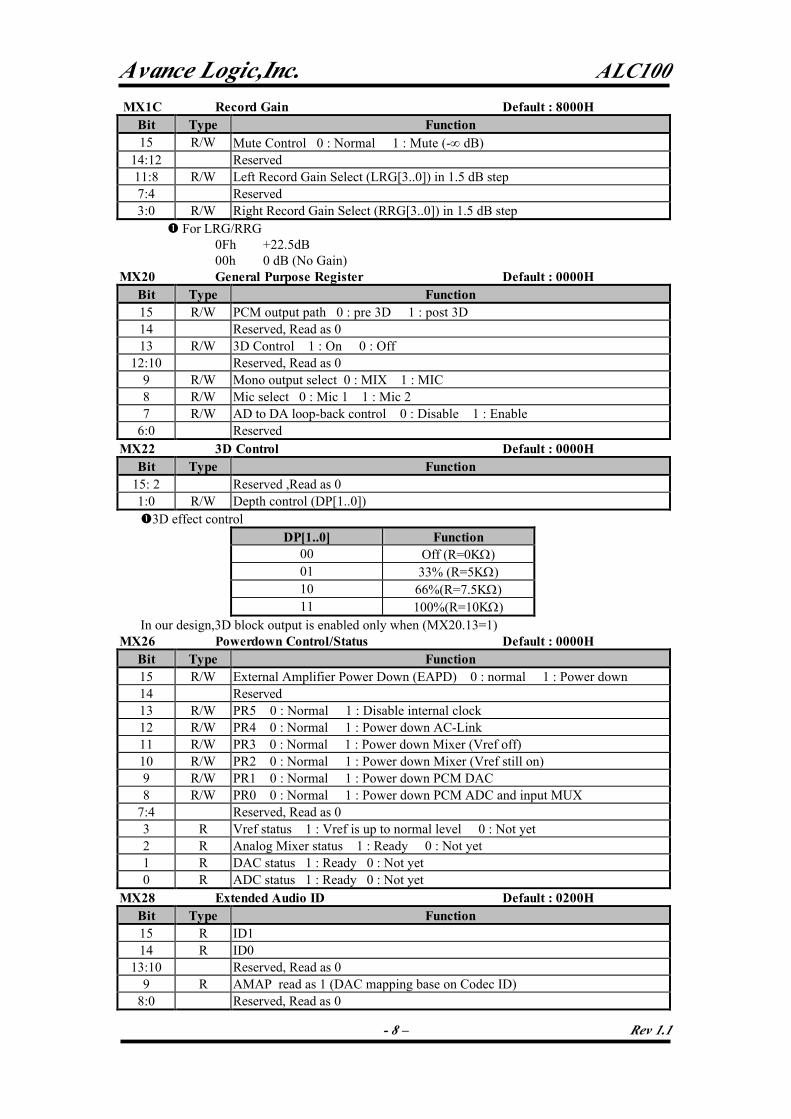
MX1C Record Gain Default : 8000HBit Type Function15 R/W Mute Control 0 : Normal 1 : Mute (-∞ dB)
14:12 Reserved11:8 R/W Left Record Gain Select (LRG[3..0]) in 1.5 dB step7:4 Reserved3:0 R/W Right Record Gain Select (RRG[3..0]) in 1.5 dB step
For LRG/RRG0Fh +22.5dB 00h 0 dB (No Gain)
MX20 General Purpose Register Default : 0000HBit Type Function15 R/W PCM output path 0 : pre 3D 1 : post 3D14 Reserved, Read as 013 R/W 3D Control 1 : On 0 : Off
12:10 Reserved, Read as 09 R/W Mono output select 0 : MIX 1 : MIC8 R/W Mic select 0 : Mic 1 1 : Mic 27 R/W AD to DA loop-back control 0 : Disable 1 : Enable
6:0 ReservedMX22 3D Control Default : 0000H
Bit Type Function15: 2 Reserved ,Read as 01:0 R/W Depth control (DP[1..0])
3D effect controlDP[1..0] Function
00 Off (R=0KΩ)01 33% (R=5KΩ)10 66%(R=7.5KΩ)11 100%(R=10KΩ)
In our design,3D block output is enabled only when (MX20.13=1)MX26 Powerdown Control/Status Default : 0000H
Bit Type Function15 R/W External Amplifier Power Down (EAPD) 0 : normal 1 : Power down14 Reserved13 R/W PR5 0 : Normal 1 : Disable internal clock12 R/W PR4 0 : Normal 1 : Power down AC-Link11 R/W PR3 0 : Normal 1 : Power down Mixer (Vref off)10 R/W PR2 0 : Normal 1 : Power down Mixer (Vref still on)9 R/W PR1 0 : Normal 1 : Power down PCM DAC8 R/W PR0 0 : Normal 1 : Power down PCM ADC and input MUX
7:4 Reserved, Read as 03 R Vref status 1 : Vref is up to normal level 0 : Not yet2 R Analog Mixer status 1 : Ready 0 : Not yet1 R DAC status 1 : Ready 0 : Not yet0 R ADC status 1 : Ready 0 : Not yet
MX28 Extended Audio ID Default : 0200HBit Type Function15 R ID114 R ID0
13:10 Reserved, Read as 09 R AMAP read as 1 (DAC mapping base on Codec ID)
8:0 Reserved, Read as 0

Avance Logic,Inc. ALC100
- 9 – Rev 1.1
ÊID1 is latched inversely from pin 46 when system reset. ID0 is latched inversely from pin 45 when system reset.ËALC100 map DAC slot according to the following table
ID[1..0] PCM Left DAC slot # PCM Right DAC slot # Comment00 3 4 Primary01 3 4 Secondary (Docking)10 7 8 Secondary (Surround)11 6 9 Secondary (Center/LFE)
MX72 Extension control register 2 Default : 1199HBit Type Function
15:14 Reserved13:12 R/W ADDA bias current 00 : 10uA 01 : 20uA 10 : 30uA 11 : 40uA11:10 Reserved
9:8 R/W Vref bias current 00 : 10uA 01 : 20uA 10 : 30uA 11 : 40uA7:6 R/W VBG control5:4 R/W VAG control 00 : 2V 01 : 2.2V 10 : 2.4V 11 : 2.6V3:2 R/W (Vrefp-Vrefn) control 00 : 0.4VAG others : 0.5VAG1:0 R/W Mixer bias current 00 : 5uA 01 : 10uA 10 : 15uA 11 : 20uA
ÊFor version latter than B, bit 3~2 are dummy and the select is always 0.5VAG.
MX7C VENDOR ID1 Default : 414CHBit Type Function15:0 R Vendor ID “AL”
MX7E VENDOR ID2 Default : 432XHBit Type Function15:8 R Vendor ID “C”7:4 R Chip ID 00103:0 R Version number 00 : version A
ÊChip ID 0010 RL5383/RL5522

Avance Logic,Inc. ALC100
- 10 – Rev 1.1
5. Design Suggestion :5.1 Clocking :
The clock source of different configuration is listed below :CODEC ID[1..0] BIT-CLK Clock source
00 Output Crystal or external clock (XTAL-IN)01 Input external clock (XTAL-IN)10 Input external clock (XTAL-IN)11 Input external clock (XTAL-IN)
5.2 AC-Link : When ALC100 take serial data from AC97 controller, it sample SDATA_OUT on the falling edge of BIT_CLK .When ALC100 send serial data to AC97 controller, it start to drive SDATA_IN on the rising edge of BIT_CLK.
ALC100 will return any uninstalled bits or registers with 0 for read operation.. ALC100 alsostuff the unimplemented slot or bit with 0 in SDATA-IN. Note that AC-LINK is MSB-justified.
Refer to “Audio CODEC ’97 Component Specification Revision 2.1” for detail.
0 1 2 3 4 5 6 7 8 9 10 11 12
TAG CMD DATA PCML PCMR
TAG ADDR DATA PCML PCMR
Fig5.2-1 ALC100 slot arrangement – CODEC ID = 00 or 01
0 1 2 3 4 5 6 7 8 9 10 11 12
TAG CMD DATA PCML PCMR
TAG ADDR DATA PCML PCMR
Fig5.2-2 ALC100 slot arrangement – CODEC ID = 10
0 1 2 3 4 5 6 7 8 9 10 11 12
TAG CMD DATA PCML PCMR
TAG ADDR DATA PCML PCMR
Fig5.2-3 ALC100 slot arrangement – CODEC ID = 11
5.3 Reset :There are 3 kinds of reset operation. Cold, Warm and Register reset which listed below :
Reset Type Trigger condition CODEC responseCold Assert RESET# for a specified period Reset all hardware logic and all registers
to it’s default value. Register Write register indexed 00h Reset all registers to it’s default value.Warm Driven SYNC high for specified period
without BIT_CLKReactivates AC-LINK, no change to register values.
The AC97 controller should drive SYNC and SDATA-OUT low during the period of RESET# assertion to guarantee ALC100 reset successfully.
5.4 CD Input :Pay attention to differential CD input. Below is an example of differential CD input.
Slot#
SYNC
SDATA-OUT
SDATA-IN
Slot#
SYNC
SDATA-OUT
SDATA-IN
Slot#
SYNC
SDATA-OUT
SDATA-IN

Avance Logic,Inc. ALC100
- 11 – Rev 1.1
Fig 5.4-1 Example of differential CD input5.5 Odd Addressed Register Access :
ALC100 will not response to odd-addressed register access for future compatibility.
5.6 Power-down Mode :Pay special attention to powerdown control register (index 26h),expecially PR4 (powerdown
AC-link).
5.7 Test Mode :5.7.1 ATE In Circuit Test Mode : SDATA_OUT is sampled high at the trailing edge of RESET#. at this mode ALC100 will drive BIT_CLK and SDATA_IN to high impedance state.5.7.2 Vendor Specific Test Mode :
SYNC is sampled high at the trailing edge of RESET#.
6. Electrical Characteristics :6.1 DC Characteristics :
Dvdd= 5.0V or 3.3V±5%, Tambient=250C, with 50pF external load.Parameter Symbol Min Typ Max Units
Input voltage range Vin -0.30 - Dvdd+0.30 VLow level input voltage Vil - - 0.35Dvdd VHigh level input voltage Vih 0.4DVdd - - VHigh level output voltage Voh 0.5DVdd - - VLow level output voltage Vol - - 0.2DVdd VInput leakage current - -10 - 10 uAOutput leakage current(Hi-Z)
- -10 - 10 uA
Output buffer drive current - - 5 - mA
6.2 AC Timing Characteristics :6.2.1 Cold Reset :
Parameter Symbol Min Typ Max UnitsRESET# active low pulse width Trst_low 1.0 - - usRESET# inactive to BIT_CLK startup delay
Trst2clk 162.8 - - ns

Avance Logic,Inc. ALC100
- 12 – Rev 1.1
Fig 6.2.1-1 Cold reset timing diagram
6.2.2 Warm Reset :
Fig 6.2.2-1 Cold reset timing diagramParameter Symbol Min Typ Max Units
SYNC active high pulse width Tsync_high 1.0 - - usSYNC inactive to BIT_CLK Startup delay
Tsync2clk 162.8 - - ns
6.2.3 AC-Link Clocks :
Fig 6.2.3-1 BIT_CLK and SYNC timing diagramParameter Symbol Min Typ Max Units
BIT_CLK frequency - 12.288 - MHzBIT_CLK period Tclk_period - 81.4 - nsBIT_CLK output jitter - - 750 psBIT_CLK high pulse width (note 2) Tclk_high 36 40.7 45 nsBIT_CLK low pulse width (note 2) Tclk_low 36 40.7 45 nsSYNC frequency - 48.0 - KHzSYNC period Tsync_period - 20.8 - usSYNC high pulse width Tsync_high - 1.3 - usSYNC low pulse width Tsync_low - 19.5 - usNote 1 : 47.5~70pF **********Note 2 : Worse case duty cycle restricted to 45/55.
6.2.4 Data Output and Input Times :

Avance Logic,Inc. ALC100
- 13 – Rev 1.1
Fig 6.2.4-1 Data Output and Input timing diagram
Parameter Symbol Min Typ Max UnitsOutput Valid Delay from rising edge of BIT_CLK
tco - - 15 ns
Note 1 : Timing is for SDATA and SYNC outputs with respect to BIT_CLK at the device driving the output.Note 2 : 50pF external load
Parameter Symbol Min Typ Max UnitsInput Setup to falling edge of BIT_CLK tsetup 10 - - nsInput Hold from falling edge of BIT_CLK thold 10 - - nsNote : Timing is for SDATA and SYNC outputs with respect to BIT_CLK at the device driving the output.
Parameter Symbol Min Typ Max UnitsBIT_CLK combined rise or fall plus flight time
- - 7 ns
SDATA combined rise or fall plus flight time
- - 7 ns
Note : Combined rise or fall plus flight times are provided for worst case scenario modeling purpose.
6.2.5 Signal Rise and Fall Times :
Fig 6.2.5-1 Signal Rise and Fall timing diagramParameter Symbol Min Typ Max Units
BIT_CLK rise time Triseclk 2 - 6 nsBIT_CLK fall time Tfallclk 2 - 6 nsSYNC rise time Trisesync 2 - 6 nsSYNC fall time Tfallsync 2 - 6 nsSDATA_IN rise time Trisedin 2 - 6 nsSDATA_IN fall time Tfalldin 2 - 6 nsSDATA_OUT rise time Trisedout 2 - 6 nsSDATA_OUT fall time Tfalldout 2 - 6 ns

Avance Logic,Inc. ALC100
- 14 – Rev 1.1
Note 1 : 50pF external loadNote 2 : rise is from 10% to 90% of Vdd (Vol to Voh)Note 3 : fall is from 90% to 10% of Vdd (Voh to Vol)
6.2.6 AC-Link Low Power Mode Timing :
Fig 6.2.6-1 AC-Link low power mode timing diagram
Parameter Symbol Min Typ Max UnitsEnd of slot 2 to BIT_CLK, SDATA_IN low
Ts2_pdown - - 1.0 us
6.2.7 ATE Test Mode :
Fig 6.2.6-1 ATE test mode timing diagram
Parameter Symbol Min Typ Max UnitsSetup to trailing edge of RESET# (also applies to SYNC)
Tsetup2rst 15.0 - - ns
Rising edge of RESET# to Hi-Z delay
Toff - - 25.0 ns
6.2.8 AC-Link IO Pin Capacitance and Loading :Output Pin 1 Codec 2 Codec 3 Codec 4 Codec
BIT_CLK (must support ≥ 2 Codecs) 55pF 55pF 62pF 70pFSDATA_IN 47.5pF 47.5pF 47.5pF 47.5pF

Avance Logic,Inc. ALC100
- 15 – Rev 1.1
7. Analog Performance Characteristics :Standard test condition : Tambient=250C, Dvdd=5.0 or 3.3V ±5%,Avdd=5.0V±5%
Input Voltage Level : Logic Low=0.35*Vdd, Logic High=0.65Vdd 1KHz input sine wave; Sampling frequency=48KHz; 0dB=1Vrms 10KΩ/50pF load; Testbench Characterization BW :20Hz~20KHz 0dB attenuation; tone and 3D disabled
Parameter Min Typ Max UnitsFull scale input voltage Line inputs Mic inputs
--
1.00.1
--
Vrms
Full scale output voltage Line output - 1.0 - VrmsAnalog S/N CD to LINE_OUT Other to LINE_OUT
90-
-85
--
dB
Analog frequency response 20 - 20,000 HzDigital S/N D/A A/D
8580
9085
--
dB
Total Harmonic Distortion Line output - - 0.02 %D/A & A/D frequency response 20 - 19,200 HzTransition Band 19,200 - 28,800 HzStop Band 28,800 - ∞ HzStop Band Rejection -74 - - dBOut-of-Band Rejection - -40 - dBGroup delay - - 1 msPower supply rejection ratio (1KHz) - -40 - dBCrosstalk between inputs channels - - -70 dBSpurious Tone Reduction - -100 - dBAttenuation, Gain Step Size - 1.5 0 dBInput impedance 10 40 - KΩInput Capacitance - 7.5 - pFVrefout - 2.25-2.75 - V

Avance Logic,Inc. ALC100
- 16 – Rev 1.1
8. Package:
MILLIMETER INCHSYMBOLMIN. TYP. MAX. MIN. TYP. MAX
A 1.60 0.063A1 0.05 0.15 0.002 0.006A2 1.35 1.40 1.45 0.053 0.055 0.057c 0.09 0.20 0.004 0.008D 9.00 BSC 0.354 BSCD1 7.00 BSC 0.276 BSCD2 5.50 0.217E 9.00 BSC 0.354 BSCE1 7.00BSC 0.276 BSCE2 5.50 0.217b 0.17 0.20 0.27 0.007 0.008 0.011e 0.50 BSC 0.016 BSC
TH 0o 3.5o 7o 0o 3.5o 7o
L 0.45 0.60 0.75 0.018 0.024 0.030