Embed Size (px)
Citation preview

AIDA-PEx: Parasitic Extraction on Layout-Aware
Analog Integrated Circuit Sizing
Bruno Cambóias Cardoso
Thesis to obtain the Master of Science Degree in
Electrical and Computing Engineering
Supervisors
Prof. Nuno Cavaco Gomes Horta
Eng. Pedro Miguel Leite Cordeiro Ventura
Eng. Ricardo Miguel Ferreira Martins
Examination Committee
Chairperson: Prof. Horácio Claúdio Campos Neto
Supervisor: Prof. Nuno Cavaco Gomes Horta
Member of the Comittee: Prof. Rui Santos-Tavares
Maio 2015


i
Abstract
The work presented in this dissertation belongs to the scientific area of electronic design
automation (EDA) and addresses the parasitic extraction in automatic sizing of analog
integrated circuits (ICs). The proposed innovative parasitic extractor, henceforward called AIDA-
PEx, was developed to be embedded in an in-house automatic layout-aware analog IC
synthesis tool, AIDA, and has the main goal of providing accurate parasitic estimates to lead
and accelerate the layout/parasitic-aware optimization of the circuit. Finding a circuit sizing
solution that fulfills all performance specifications after circuit layout is a time-consuming task
that requires non-systematic iterations between electrical and physical design steps, which
increases the design time of analog ICs. Moreover, the performance of automatic layout-aware
IC sizing methodologies is heavily dependent on the promptitude of the iterations. The in-loop
evaluation of each tentative solution encompasses three main steps: circuit simulation, layout
generation and parasitic extraction. The proposed approach, unlike previous approaches
available in the literature, estimates the parasitic capacitances and resistances from a simplified
layout that includes the floorplan and a non-detailed routing, using an empirical-based method
supported by the data from the technology design kit (TDK) files. AIDA-PEx uses the provided
empirical data and geometrical considerations to model the parasitic components of the devices’
terminals and routing paths for a complete 2.5-D extraction. Experimental results are presented
for the United Microelectronics Corporations (UMC) 0.13μm design process and compared with
the industry standard parasitic extractor Mentor Graphics’ Calibre®, which showed that 90% of
the solutions needed the layout-aware approach to assure a correct post-layout simulation that
meets all the specifications.
Keywords
Analog Integrated Circuits Design
Computer-Aided Design
Electronic Design Automation
Layout-Aware Circuit Sizing
Parasitic Extraction

ii

iii
Resumo
O trabalho descrito nesta dissertação enquadra-se na área científica de automação de projecto
eletrónico, e foca a extração de parasitas no contexto do dimensionamento automático dos
componentes de circuitos integrados analógicos. Encontrar uma solução para o
dimensionamento do circuito que cumpra todas as especificações de performance depois da
geração do layout é um processo demorado, que necessita de iterações não sistemáticas entre
fases de projeto elétricas e físicas, o que aumenta bastante o tempo de desenvolvimento do
projeto. No entanto, a performance de metodologias automáticas de dimensionamento de
circuitos integrados com inclusão de componentes do layout é extremamente dependente da
rapidez de execução das iterações. A avaliação de cada solução encontrada dentro do ciclo de
otimização engloba três etapas principais: simulação do circuito, geração do layout e extração
de parasitas. O extrator de parasitas proposto, denominado AIDA-PEx, foi desenvolvido com o
intuito de ser embebido numa ferramenta de dimensionamento automático de circuitos
integrados analógicos que incluí informação do layout durante a otimização, AIDA. O AIDA-Pex
tem como objetivo principal fornecer estimativas precisas de componentes parasitas de modo a
conduzir rapidamente o processo da otimização do circuito. Ao contrário de outros métodos
disponíveis na literatura, o AIDA-Pex estima as capacidades e resistências de um layout
simplificado que incluí os dispositivos e uma versão não detalhada das ligações entre eles,
utilizando um método empírico suportado pelos dados retirados dos ficheiros da tecnologia. O
AIDA-PEx usa os dados empíricos fornecidos juntamente com considerações geométricas para
modelar os componentes parasitas num modelo 2.5-D. Os resultados experimentais são
apresentados para o processo de dimensionamento da United Microelectronics Corporations
(UMC) 0.13μm, e comparados com o extrator de parasitas Mentor Graphics’ Calibre®,
referência nesta indústria. Nestes testes, 90% das soluções obtidas com a otimização
tradicional não cumpriam as especificações depois do layout, comprovando a importância da
metodologia proposta.
Palavras-Chave
Projecto de Circuitos Integrados Analógicos
Projecto Assistido por Computadores
Automação de Projecto Eletrónico
Dimensionamento de Circuitos tendo em conta efeitos da Representação Física
Extracção de Parasitas

iv

v
Acknowledgements
I would like to acknowledge my supervisor Prof. Nuno C. G. Horta for the support, guidance and
motivation during the development of this project at Instituto de Telecomunicações. I would also
like to leave a special word of gratitude to Ricardo Martins and Nuno Lourenço for the guidance
and never-ending will to help. Their support and inspiration made this tough and challenging
journey that much easier.
I would also like to present a word of recognition to all involved in the AIDA project: Ricardo
Póvoa, António Canelas, Pedro Ventura and Jorge Guilherme, whose ideas and discussions
turned out very valuable to the progress of this work.
Finally to my family, especially my mother and sister, and friends for the never-ending support
and understanding since day one.

vi

vii
Table of Contents
Abstract .......................................................................................................................................... i
Keywords ........................................................................................................................................ i
Resumo ......................................................................................................................................... iii
Palavras-Chave ............................................................................................................................. iii
Acknowledgements ....................................................................................................................... v
Table of Contents ......................................................................................................................... vii
List of Tables .................................................................................................................................. ix
List of Figures ................................................................................................................................ xi
List of Abbreviations .................................................................................................................... xiii
Chapter 1 Introduction ................................................................................................................ 1
1.1 Motivation ...................................................................................................................... 2
1.2 Research Goals ............................................................................................................. 3
1.3 Contributions ................................................................................................................. 4
1.4 Document Structure....................................................................................................... 5
Chapter 2 State-of-the-Art .......................................................................................................... 7
2.1 Layout-aware Analog Synthesis .................................................................................... 7
2.2 Parasitic Extraction ...................................................................................................... 10
2.3 Standard Industry Tools ............................................................................................... 14
2.4 Conclusions ................................................................................................................. 15
Chapter 3 AIDA’s Synthesis Flow ............................................................................................. 17
3.1 Integration on AIDA Framework .................................................................................. 17
3.2 AIDA-PEx Architecture ................................................................................................ 19
3.2.1 Inputs ....................................................................................................................... 19
3.2.2 Technology Design Kit Processing .......................................................................... 21
3.2.3 Parasitic Extraction .................................................................................................. 21
3.2.4 Outputs .................................................................................................................... 22
3.3 Conclusions ................................................................................................................. 23

viii
Chapter 4 TDK Processing ....................................................................................................... 25
4.1 TDK tables ................................................................................................................... 26
4.2 Preliminary tests .......................................................................................................... 31
4.2.1 Case Study I: Two parallel stripes of Metal (1, 4, 8) ................................................ 31
4.2.2 Case Study II: Stripe of Metal X above a Stripe of Metal 1 (parallel) ...................... 34
4.2.3 Case Study III: Stripe of Metal 2 above a Stripe of Metal 1 (perpendicular) ........... 35
4.3 Conclusions ................................................................................................................. 37
Chapter 5 Parasitic Extraction .................................................................................................. 39
5.1 Parasitic Resistance .................................................................................................... 40
5.2 Parasitic Capacitance .................................................................................................. 41
5.2.1 Substrate Capacitance (CS)..................................................................................... 41
5.2.2 Interconnect Capacitance (CI) ................................................................................. 42
5.3 Geometrical considerations ......................................................................................... 46
5.4 Preliminary Tests ......................................................................................................... 47
5.5 Conclusions ................................................................................................................. 48
Chapter 6 Results ..................................................................................................................... 49
6.1 Case Study I – Single Ended 2-Stage Amplifier .......................................................... 49
6.2 Case Study II – 2-Stage Folded Cascode Amplifier .................................................... 53
6.3 Conclusions ................................................................................................................. 55
Chapter 7 Conclusions and Future Work ................................................................................. 57
7.1 Conclusions ................................................................................................................. 57
7.2 Future Work ................................................................................................................. 57
Chapter 8 References .............................................................................................................. 59

ix
List of Tables
Table 2-1 – Comparison between state-of-the-art works on layout-aware sizing with special
detail to layout-related data. .......................................................................................................... 9
Table 4-1 – Results for Case Study I. ......................................................................................... 32
Table 4-2 – Results for parallel slide. .......................................................................................... 33
Table 4-3 – Results for perpendicular slide. ................................................................................ 34
Table 4-4 – Results for Case Study II (Part I). ............................................................................ 35
Table 4-5 – Results for Case Study II (Part II). ........................................................................... 36
Table 4-6 – Results for Case Study III. ....................................................................................... 37
Table 5-1 – Intra-module Capacitance Comparison. .................................................................. 48
Table 6-1 – Direct Bulk Capacitance Comparison. ..................................................................... 50
Table 6-2 – Direct Interconnect Capacitance Comparison for 51dB Layout. .............................. 50
Table 6-3 – Direct Interconnect Capacitance Comparison for 75dB Layout. .............................. 51
Table 6-4 – Pre/Post-Layout Simulation. .................................................................................... 51
Table 6-5 – Illustration of resulted layouts for the 51dB circuit. .................................................. 52
Table 6-6 – Illustration of resulted layouts for 75dB circuit. ........................................................ 53
Table 6-7 – Performance Comparison for the traditional and layout-aware optimizations. ........ 54

x

xi
List of Figures
Figure 1-1 – Traditional Analog IC Design Flow. .......................................................................... 2
Figure 1-2 – Layout-aware loop in optimization-based sizing. ...................................................... 3
Figure 2-1 – Electric field lines on conductors storing different charges..................................... 11
Figure 2-2 –The various capacitances considered in 2.5-D modeling. ....................................... 12
Figure 2-3 – 3-D modeling as a combination of two 2-D structures. ........................................... 13
Figure 2-4 – Mentor Graphics’ Calibre® parasitic extraction GUI [4]. ......................................... 15
Figure 3-1 – AIDAsoft website [29].............................................................................................. 17
Figure 3-2 – AIDA Layout-aware Environment. .......................................................................... 18
Figure 3-3 – AIDA-PEx architecture. ........................................................................................... 20
Figure 3-4 – Router output comparison. ..................................................................................... 20
Figure 3-5 – Parasitic netlist example with π2 model. ................................................................ 22
Figure 4-1 – TDK Processing architecture: Interpolation and Empirical Models. ....................... 25
Figure 4-2 – Example of a foundry table, metal1 above substrate (M1/ SUB) for the UMC
130nm. ......................................................................................................................................... 26
Figure 4-3 – 3-D representation of Area Capacitance. ............................................................... 27
Figure 4-4 – 3-D representation of Fringe Capacitance. ............................................................. 27
Figure 4-5 – 3-D representation of Coupling Capacitance. ......................................................... 28
Figure 4-6 – 2-D representation of Area Capacitance. ............................................................... 28
Figure 4-7 – Linear-by-segments interpolation of Area Capacitance. ......................................... 29
Figure 4-8 – 2-D representation of Fringe Capacitance. ............................................................. 29
Figure 4-9 – Linear-by-segments interpolation of Fringe Capacitance. ...................................... 30
Figure 4-10 – 2-D representation of Coupling Capacitance. ....................................................... 30

xii
Figure 4-11 – Linear-by-segments interpolation of Coupling Capacitance. ................................ 31
Figure 4-12 – Capacitances considered on Case Study I. .......................................................... 32
Figure 4-13 – Geometrical parameters on parallel slide. ............................................................ 32
Figure 4-14 – Geometrical parameters on perpendicular slide. .................................................. 33
Figure 4-15 – Parameters took into account on Case Study II. .................................................. 35
Figure 4-16 – Parameters took into account on Case Study III. ................................................. 36
Figure 5-1 –Parasitic extractor architecture: Resistance Modeling, Capacitance Modeling,
Geometrical Considerations. ....................................................................................................... 39
Figure 5-2 – Intrinsic resistance of a conductor. ......................................................................... 40
Figure 5-3 –Parasitic wire resistance computed by square counting [3]. ................................... 41
Figure 5-4 – Capacitances considered to compute substrate capacitance. ............................... 42
Figure 5-5 – Capacitances considered for interconnect capacitance on the same layer. .......... 43
Figure 5-6 – Interconnect capacitance for overlapping plates (2D view). ................................... 44
Figure 5-7 – Interconnect capacitance for non-overlapping plates (3D view). ............................ 44
Figure 5-8 – CF decay with respect to the space between conductors. ...................................... 44
Figure 5-9 – CF decay with respect to the lower plate’s width. ................................................... 45
Figure 5-10 – Top view example of space occupation analysis. ................................................. 46
Figure 6-1 – Single ended 2-stage amplifier used as respective POF........................................ 49
Figure 6-2 – Traditional and Layout-aware optimization POFs (Case Study I). ......................... 52
Figure 6-3 –2-stage folded cascode amplifier. ............................................................................ 54
Figure 6-4 – Traditional and Layout-aware optimization POFs (Case Study II). ........................ 55
Figure 6-5 –Illustration of resulted layouts (Case Study II). ........................................................ 55

xiii
List of Abbreviations
CAD Computer-Aided-Design
CMOS Complementary Metal Oxide Semiconductor
DRC Design Rule Check
DSM Deep-SubMicrometer
DSP Digital Signal Processing
EDA Electronic Design Automation
GUI Graphical User Interface
IC Integrated Circuit
LVS Layout Versus Schematic
POF Pareto Optimal Front
RF Radio-Frequency
SoC System-on-a-Chip
TDK Technology Design Kit
UMC United Microelectronics Corporations
VLSI Very Large Scale Integration

xiv

1
Chapter 1 Introduction
This chapter presents a brief introduction to the traditional analog integrated circuit design flow
and to electronic design automation with particular emphasis on layout-aware sizing
methodologies, which are the focus of this work. Then, the motivation for this dissertation is
presented, and, finally, the research goals and contributions are outlined.
In the recent past, the ever-increasing demand for microelectronic devices led to the massive
improvement in the area of Very Large Scale Integration (VLSI) technologies, allowing the
proliferation of consumer electronics and enabling the steady growth of the Integrated Circuits
(ICs) market. The increase in IC complexity is mostly supported by an exponential growth in the
density of transistors while inversely reducing the transistors’ cost, which allows the designers to
build multimillion transistor ICs. This increase in the design complexity is only possible to follow
because IC designers are assisted by Computer Aided Design (CAD) tools that support the
design process [1][2].
Most functions in today’s ICs are implemented using digital or Digital Signal Processing (DSP)
circuitry, and, although analog blocks constitute only a small fraction of the components on
mixed-signal ICs and system-on-a-chip (SoC) designs they still play a major role. Analog ICs
are known for its difficult re-utilization, so designers have been replacing analog circuit functions
for digital computations, however, there are some blocks that stubbornly remain analog, e.g.,
sensor interfaces, sample-and-hold circuits, analog-to-digital converters and frequency
synthesizers.
Unlike digital circuits, where the low-level phases of the design process are automated using
fairly standard methodologies, the synthesis and layout of analog circuits is most of the time a
manual task. The absence of mature design automation tools creates a great dependence on
human intervention in all phases of the design process, which, despite being supported by
circuit simulators, layout editing environment and verification tools, results in a time-consuming
and error-prone design flow when compared to the development time of the digital blocks.
Despite the advantages that the new fabrication technologies bring to IC performance, the
reduced size and high density of devices, especially in modern analog ICs, add new challenges
to analog designers. The effects of non-idealities, variability of the fabrication process
parameters and circuit’s parasitics causes disturbances that, if not being weighted in the early
stages of development, can be responsible for design errors and expensive re-design cycles,
becoming the bottleneck of SoC and mixed-signal ICs design.
Traditionally, the design flow of analog ICs starts with the topology selection, where the user
determines the most appropriate circuit topology in order to meet a set of given specifications.

2
Given a selected topology, the specifications are translated from system-level to cell-level,
where the task is reduced to circuit sizing. At each specification translation step the circuit is
tested and resized until all the initial specifications are met. When the obtained circuit meets the
desired performance, the next task of the design flow is the layout synthesis, in which the
fabrication masks that are used to produce the devices are drawn using the sizes obtained from
the previous step, as illustrated in Figure 1-1.
CircuitSpecifications
SchematicManualSizing
PerformanceSimulation
FEASIBLE ? ManualLayout
DRCLVS
Parasitics
Post-LayoutSimulation
NO YES
Manufacturing
FEASIBLE ?
NO
YES
Circuit
Phase
Physical
Phase
Figure 1-1 – Traditional Analog IC Design Flow.
In this traditional flow, the layout generation task is only triggered when the sizing task is
complete, but in order to overcome the increasing impact of layout parasitic effects in circuit's
performance, sizing and layout design phases tend to overlap with non-systematic iterations
between these electrical and physical design steps. If these effects are not accounted for, the
circuits’ post-layout performance can be compromised, and, if the circuit is wittingly
overdesigned the result is a waste in power and area. Furthermore, even the evaluation of the
circuit area or aspect ratio is practically impossible from the netlist alone without any layout
generation.
1.1 Motivation
In digital IC design several Electronic Design Automation (EDA) tools and design methodologies
are available to help the designers keeping up with the new capabilities offered by the
integration technologies, while analog design automation tools are not keeping up with the new
challenges created by technological evolution. This lack of automation drives analog designers
to manually explore the solution space searching for a solution that fulfills the design
specification, a task that’s both exhaustive and time consuming, not to mention that even if the
solution is found, it rarely is the optimal solution. Optimization-based tools are of the utmost help
to analog IC designers, not only accelerating the sizing process, but also providing reliable
solutions.
Hence, to address post-layout performance degradation and geometric requirements earlier in

3
the design flow, the, so called, layout-aware or layout-driven design approaches automatically
include layout effects during the automatic sizing loop, to trim down the effects of high-order
non-idealities and parasitic disturbances that affect analog circuits' performance. However, to
achieve post-layout successful designs that meet all specifications, time-consuming tasks like
layout generation and parasitic extraction are required inside the sizing loop, as sketched in
Figure 1-2. This time cost will affect the optimization loop delaying each iteration, and
consequently, exponentially increasing total runtime.
Layout
Syntthesis
Parasitic
Extraction
Performance
Simulation
Optimization-based Circuit Sizing
Figure 1-2 – Layout-aware loop in optimization-based sizing.
There are several existing commercial tools to accurately extract the circuit parasitics (ANSYS
Q3D, StarRC, QRC, Calibre, etc.). The problem using these extractors, in the automatic sizing
loop, is either the setup time required to have the entire Design Rule Check (DRC) and Layout
Versus Schematic (LVS)-clean layout coded in a procedural generator, which should also be
flexible to accommodate different placement and routing layouts, or the execution time required
to obtain the complete full layout design using a custom generator, which is one of the most
time consuming tasks on the automatic analog layout flow [3].
1.2 Research Goals
Innovative layout-aware sizing methodologies are emerging in the EDA community and
represent an important part of the future of analog design automation, closing the gap between
electrical and physical design for a unified sizing and layout process. Fast, flexible and complete
layout generation and parasitic extraction techniques are required to promptly include layout-
related data into the sizing process, however, these are usually exhaustive and time consuming
tasks in both manual and automation realities. In order to overcome these problems, the
automatic flow proposed in [3] shows the advantages of the layout-aware approach using a
simplified layout description enhanced with quick estimates for parasitics, but the truth is that
designers’ trust is in the industry “standard” extraction tools.

4
The methodology presented in this document focuses on the parasitic extraction task of analog
ICs, however, the main goal of this work is to enable the layout-aware optimization task to be
more precise and robust, with a lightweight parasitic extractor that accurately estimates the
effects of non-idealities in the layout and leads the optimization of the circuit. In this context, a
customized tool is then of utmost relevance to a correct and fast parasitic estimation. The goals
of this research can be summarized as:
To create a fast parasitic extractor that can be embedded in a layout-aware analog IC
optimization loop without compromising running time. However, in order to meet the
designers’ expectations, it is important to have results with high accuracy, i.e.,
comparable with the results of an industry-standard commercial extractor; hence it must
also be accurate in estimating the values of the parasitics to properly lead the circuit’s
optimization.
To determine the set of parasitic capacitances and resistances that further influence the
group of studied circuits (class of analog amplifiers and similar). Experimental tests to
partial layouts have been done with this purpose (layouts containing only devices, only
routing paths, etc.);
To develop a set of heuristics that are able to run accurately not only over the complete
layout, but also over the incomplete layout, which has only the global routing, and is
used in the optimization loop to accelerate the process. Currently, extractors integrated
in layout-aware methodologies can only operate over complete layout descriptions;
To approximate as much as possible the estimated parasitic components from the ones
extracted by an off-the-shelf commercial tool. Even though the results from the
developed module are extracted from an early-stage of the layout instead of the
complete and detailed layout.
1.3 Contributions
The primary goals of AIDA-PEx, the proposed extractor, are to be fast and precise that can be
introduced in the optimization loop with the upmost confidence. Most approaches where
parasitic extraction has high accuracy require the complete full layout design with detailed
routing, which is one of the most time consuming tasks on the automatic analog layout flow.
Moreover, these approaches rely on procedural layout generators that lack on flexibility to
handle specification or topological changes. In order to accelerate in-loop process, AIDA
generates a simplified routing that only sketches the routing paths in metal1 stripes and extracts
the parasitic layout components from them. Therefore, a major contribution of AIDA-PEx is

5
being able to work over a complete detailed layout as well as over the simplistic layout
generated in the optimization loop.
AIDA-PEx was tested and validated with a set of operational amplifier circuits for the UMC
0.13µm process and compared with the industry standard Mentor Graphics’ Calibre®, ensuring
high accuracy even when running over the simplified layout, used in the optimization loop. By
considering new accurate models for the technology dependent parameters, a new computation
of substrate and interconnect capacitance and new geometrical considerations, a complete
parasitic extractor is implemented that guarantees fast and solid results.
These characteristics empower the optimization process when AIDA-PEx is integrated in the
loop, allowing the performance measurements to be more realistic and precise. The layout-
aware sizing task culminates in optimal and robust solutions. The promising achieved results led
to a paper submission:
B. Cardoso, R. Martins, N. Lourenço and N. Horta, “AIDA-PEx: Accurate Parasitic
Extraction for Layout-Aware Analog Integrated Circuit Sizing,” in IEEE PhD Research in
Microelectronics and Electronics (PRIME), Glasgow, Scotland, July 2015 (Submitted on
March 2015).
1.4 Document Structure
The rest of this document is organized as follows:
Chapter 2 presents an overview of the state-of-the-art in layout-aware analog integrated
circuit sizing, focusing on the layout generation approaches and parasitic extraction
methods that are used.
Chapter 3 sketches the flow of AIDA, specifying the different tasks of each module. It
also presents a brief introduction to AIDA-PEx architecture.
Chapter 4 describes the empirical data used to compute the parasitic components,
illustrating the variation of the values according to the look-up variables and explaining
the chosen regression.
Chapter 5 details the approach chosen to create the extractor, showing the different
considerations that led to the modeling, computation and approximation of the
estimated capacitances.
Chapter 6 presents some case studies to test the parasitic extraction and consequent
extracted netlist performance simulation. The results are compared with Mentor
Graphics’ Calibre® [4].
Chapter 7 addresses the closing remarks and some directions for future developments
are suggested.

6

7
Chapter 2 State-of-the-Art
This chapter starts by addressing the state-of-the-art in Layout-Aware Analog Synthesis and in
the second section an overview of the past works and approaches on accurate/fast parasitic
extraction is presented.
2.1 Layout-aware Analog Synthesis
In the past few years, several tools that implement a layout-aware analog synthesis of ICs have
emerged. Yet, in most of them the process is not completely automatic, with various phases still
requiring user input and handmade design, either on circuit sizing or layout generation.
The behavior of analog circuits is extremely sensitive to layout-induced parasitics. Parasitics not
only influence the circuit performance but often render it non-functional. Hence, it is essential to
consider the effect of parasitics early in the design process. Traditionally, the circuit synthesis
step is followed by layout synthesis and each step is carried out independent of the other. This
is followed by a verification step to check whether the desired performance goals have been
achieved after layout generation and extraction. These steps are carried out iteratively until the
desired performance goals are met. This approach is extremely time-consuming and no
structured feedback from previous runs can be readily used to re-design the circuit if the layout
fails to meet performance goals. One way of performing layout-aware synthesis is to perform
layout synthesis and extraction inside the circuit synthesis loop, so fast procedural layout
generators are generally used.
Vancoreland et al. [5] uses genetic algorithms with manually derived performance models to
evaluate the circuit parameters. Integrated in the loop, the layout is created with a procedural
generator and geometric data is obtained with sculptured equations. Fitted functions are used to
test the performance of the circuit and the data related to the parasitics of the layout is extracted
by a 1-D/2-D modeling but only applied for the area and fringing capacitance of the metal1 and
poly stripes of the circuit’s critical nets.
Ranjan et al. [6] uses pre-compiled symbolic performance models to evaluate the circuit’s
performance at each iteration of the loop, thus avoiding numerical simulation. To this models are
passed the area and interconnect parasitic values along with the passive component values.
The layout is rapidly created with a parameterized procedural generator which consists on a
fixed template layout, which serves as a blueprint to the mapping of the components, which are
instantiated when the parameters of the circuit are given. The circuit’s parasitics are obtained
using an external extractor.
Pradhan et al. [7] starts by sampling a design space to generate circuit matrix models that can

8
predict the circuit performance at each iteration. For a uniform number of design points, a
procedural generator creates layout samples (it doesn't actually generate the complete layout
in-loop to reduce iteration time), and bulk, device and interconnect parasitics are modeled by
linear regression. With the goal of optimizing conflicting performance objectives, it creates a
Pareto-optimal surface with points spread uniformly in all regions.
Youssef et al. [8] implements a simulation-based circuit synthesizer. A Python-based procedural
layout generator ensures different layout styles for the same analog blocks, opening the results
to some variation on the optimization variables. The layout-related data addressed by the
generation tool includes modeling of the stress effects of the devices and some geometrical
measures, using analytical models to obtain the values for the circuit’s parasitics.
Habal et al. [9] uses a deterministic placer where every possible layout for each device in the
circuit is generated and investigated using a placement algorithm Plantage [10]. The layouts
with undesirable geometric features are then discarded and only the final selected placement
based on area, electrical performance and aspect ratio is routed. Designer knowledge is
supplied by geometric circuit placement and routing constraints, then a deterministic nonlinear
optimization algorithm is used for circuit sizing. A complete extraction of circuit’s parasitics is
made using Cadence Assura®.
Castro-Lopez et al. [11][12] deals with both parasitic-aware and geometrically constrained
sizing, creating new optimization variables which can therefore include solutions for optimized
area and shape of the total circuit. Using commercially available tools to evaluate the
performance of the circuit, it attains highly integrated solutions by creating a coded slicing-tree
to generate a predefined template. The templates implemented by using the Cadence pCells
technology and SKILL programming avoid long iteration times. Without actually generating the
layout, 3-D parasitic estimation was achieved with template sampling techniques and analytical
equations.
Liao et al. [13] implements a user assisted tool, where designer decision and knowledge is
inputted during circuit sizing and layout template configuration. The program uses analytical
models for the layout-related data, where polynomial equations derive the values of the
capacitances from geometrical data, from the layout template, and technology parameters.
A synopsis of all these works is presented in Table 2-1, with special attention to the provided
layout-related data.

9
Table 2-1 – Comparison between state-of-the-art works on layout-aware sizing with special detail to layout-related data.
Work Circuit
Synthesizer Performance Evaluation
Layout Generator Layout-related Data
Placer Router Geometric
Parasitics Included
Observations Bulk
Intra-Device
Inter-Device
Routing Wires
Resistances
Vancorenland et al. [5]
Performance models and
Genetic algorithms
Fitted functions Procedural generator Equations Gate 1/2-D analytical-geometrical modeling
of the critical nets
Ranjan et al. [6]
Optimization-based
Symbolic models Procedural generator (design space
sampled) No
Area and interconnect using external extractor
Pradhan
et al. [7]
Multi-objective Opt.
Symbolic models Procedural generator (design space
sampled) No
Analytical models for bulk, device and interconnect
Youssef et al. [8]
Simulation-based Opt.
Circuit simulation and
Design plans Procedural generator Yes
Modeling of the stress effects of the devices
Habal et al. [9]
Simulation-based
Deterministic nonlinear
Circuit simulation Enumeration of all possible
floorplans
Exhaustive setup for Cadence Chip
Assembly Router® Yes
Complete extraction using Cadence Assura®
Lopez
et al. [11][12]
Simulation-based
Multi-objective Opt.
Simulation (Spectre® or HSPICE®)
Coded Slicing-tree
Template-based Yes 3-D analytical-geometrical
Liao
et al. [13] User Assisted Yes
Analytical models for area and interconnect
This work, AIDA
Simulation-based
Multi-objective Opt.
Worst case corner simulation
(Spectre®, Eldo® or HSPICE®)
Multiple B*-trees
Automatic electromigration-
aware wiring topology and global routing in-
loop
Yes 2.5-D modeling of the devices and routing
that operates over non-detailed routing

10
In [5][6][7][8] procedural generators are used (in-loop or for layout sampling), on which the
whole layout of the circuit is coded and require huge setup times. Furthermore, these don’t
support wide specification changes, and, if any topology or technology changes are necessary a
complete setup/re-design of the circuit is inevitable.
In [11][12] the flexibility of the layout generator is improved by the use of a template-based
approach supported on a slicing model, but due to the multitude of different sizing solutions
found throughout the whole Pareto solution set it is almost impossible to pack all the solutions
properly with the same fixed template. The alternative presented in [9] is fully automatic
generation with an exhaustive search, but costing the increase in computation time. However,
for all approaches, routing template is the same for all design solutions and is not fitted to the
solutions as they vary in a multitude of devices’ sizes/shapes and performances.
In [5] a 1/2-D analytical-geometrical model was chosen for parasitic estimation, but it is only
applied for the area and fringing capacitance of the metal1 and poly stripes of the circuit’s
critical net(s), which makes the estimation quick, but loses accuracy and needs user
intervention to identify the critical net(s). This can lead to errors, if, depending on layout, less
critical nets became problematic.
In [7][11][12][13] analytical polynomial models with predictor variables, such as diffusion
area/perimeter or even voltages/ currents from circuit simulation are used, yielding a very fast
estimation of the parasitic impact on circuit’s performance without post-layout simulation. Still
these values are just predictions and can have a large error. In [8] analytical models are also
used, but the predictor variables related to the transistors’ stress effects, which are distances
between components, do require some post-layout analysis.
In [6][9] an external extractor is used which guarantees accurate results for the parasitic
estimation. Although the parasitics obtained by using these techniques are very accurate, their
inclusion in the optimization loop either forces the creation of a custom parameterized layout,
which adds considerable setup time, or using custom full layout generator, which is prohibitively
slow to use inside the optimization loop.
2.2 Parasitic Extraction
Parasitic effects are becoming more critical with the increase in performance, density,
complexity and levels of integration in deep-submicrometer (DSM) designs. In IC design, the
final area occupied by the elements of the circuit is often one of the optimization variables,
which every designer wants to minimize. With that in mind, designers place the components as
closer as they can, following the DRC rules, leading to very compact floorplans. In this
subsection the main works on parasitic extraction are outlined and analyzed.

11
A parasitic element arises due to the proximity of conductors or the lengths of traces, wires, or
leads of components, because when two conductors at different potentials are close to one
another, they are affected by each other’s electric field and store opposite electric charges,
forming a capacitor, as illustrated in Figure 2-1.
Figure 2-1 – Electric field lines on conductors storing different charges.
A conductor (or terminal) has an intrinsic capacitance relative to the substrate and an
interconnect capacitance concerning each one of the nearby conductors. Depending on the
relative positioning of the conductors at issue, many situations can arise, leading to different
classifications to the existing capacitances.
There are three primitive capacitance classifications: Area Capacitance (CA), Fringe
Capacitance (CF) and Coupling Capacitance (CC), as illustrated in Figure 2-2. Coupling
capacitance is only present when the evaluation is being conducted between conductors in the
same layer. Area capacitance is only present when two conductors in different layers overlap,
corresponding to the field lines existent in the area on which these conductors overlap. Fringe
capacitance refers to the rest of the lines that curve around the conductors. With an important
role in parasitic estimation, fringe capacitance is the hardest to understand and estimate, due to
the geometrical implications it requires.
Even though the latest processing technology advancements on lowering the relative constant
of the dielectric reduce the effect of the parasitic capacitances, the continued scaling down of
the feature size keeps the parasitic effects dominant. The capacitance extraction advanced from
1-D, 2-D, quasi-3-D (or 2.5-D) to 3-D effects to meet the required accuracy.

12
Figure 2-2 –The various capacitances considered in 2.5-D modeling.
In the first approaches a 1-D capacitance extraction was used, which calculates the values by
weighting the area and perimeter of interconnect geometries into an expression (only CA
component). Then, 2-D extraction was introduced where the parameters set is extended to
account for the same layer capacitive effect. In other words, not only conductor’s overlap CA is
addressed but also the effect two conductors in the same layer have on each other, i.e., CC
component.
Still, the 2-D approaches doesn’t cover the effect of 3-D structures such as two wires crossing,
so a 3-D pattern is needed to address the non-overlapping capacitance between interconnects
of different layers. However, there are numerous variations in 3-D structures and 3-D
capacitance extractors are not trivial extensions of 2-D ones.
An extension to address 3-D effects is the 2.5-D method, where the 3-D effect is modeled as a
combination of two orthogonal 2-D structures [14], as it is illustrated in Figure 2-3. By carefully
composing a 3-D solution from the two orthogonal 2-D ones, most 3-D effects are captured,
avoiding the complicated 3-D evaluation.
The 3-D modeling is always complicated due to the geometrical implications it requires. From
the basic capacitances used to compute the more complex ones, only fringe capacitance is
challenging to modulate precisely because of the geometrical considerations needed to
correctly estimate the values. The area and coupling capacitance have well defined areas of
effect, but for fringe capacitance this area is not so well delimited.

13
M2
M1
M1
M2 M2
(a) Top View (b) Cross section view 1 (c) Cross section view 2
Figure 2-3 – 3-D modeling as a combination of two 2-D structures.
In past years, many works on accurately modulating the fringe capacitance were developed.
Bansal et al. [15] proposed an analytical model to compute the fringe capacitance between two
non-overlapping interconnects in different layers using a conformal mapping technique. These
models are derived by analyzing the electrostatics between interconnects and using technology-
dependent parameters. The conformal mapping technique replicates the characteristics of the
electrical field lines between conductors to modulate the effect of fringe capacitance.
More recently, Shomalnasab et al. [16] took this idea to modulate fringe capacitance based on
electric flux and applied it on interconnect estimation, in the same layer or in different layers. In
this technique, massive geometrical considerations are needed along with technology
dependent data. First, a general template for the fringe capacitance based on fundamental
electromagnetic principals is derived, and then, the accuracy is improved with a fitting
technique.
Following the analytical approach, Sharma et al. [17] presented closed-form analytical
expressions for interconnect parasitic capacitances in VLSI, derived from variation analysis.
Although analytical models can be very accurate, the implications they would bring for more
complex modules (common centroid, etc.) and the difficulty of deriving the technology related
parameters, make the use of these techniques inside an optimization loop impracticable.
There are a few works that, trying to accelerate the process, estimate the different capacitances
even before complete layout generation. Yu et al. [18] created a 2-D pattern characterization for
pre-route stage, with a pattern-library method. Then circuit’s congestion is estimated and linear
interpolation is carried over a conductors’ width variable. In this work, resistances are calculated
with analytical equations. Trying to estimate the values for the capacitances even earlier, Foo et
al. [19] derives parasitics evaluating floorplan density. A look-up table is then created mapping
each density reading to an appropriate spacing value.
Vemuri et al. [20][21] was the first to study parasitic extraction with the purpose of embedding it

14
in a layout-aware sizing approach, not only regarding the resulted accuracy, but also the
extraction runtime. This work uses an empirical method, where massive look-up tables are
accessed to estimate the parasitic components. Additionally, the data is processed with
determinant decision and multi-variable linear interpolation. This approach might not achieve
such higher levels of accuracy but it is a fast method for parasitic component estimation.
In order to achieve ultimate levels of accuracy, Karsilayan et al. [22] calibrates a set of various
analytical equations based on layout parameters. Additionally, a field solver is used, which is a
specialized program to directly solve a subset of Maxwell’s equations [23]. The 2-D field solver
provides capacitance and sensitivity data to fit the layout parameters to the analytical formulas,
resulting in a 2.5-D parasitic extraction framework.
This work was applied in Mentor Graphics’ Calibre®, which is one of the available industry tools
for parasitic extraction in the market. In the next subsection, the off-the-shelf parasitic
extraction/estimation tools are outlined.
2.3 Standard Industry Tools
In the recent past years, several commercial tools have emerged in the analog layout EDA
market to estimate parasitics, and even though the methods and formulations they implement
are still secret for business reasons, some brief specifications are presented next:
ANSYS Q3D Extractor [24]: uses a method of moments (integral equations) to
compute capacitive, conductance, inductance and resistance matrices.
FastCap, FastHenry [25]: from MIT (Massachusetts Institute of Technology) are two
free parasitic extractor tools for capacitance, inductance and resistance. Quoted in
many scientific articles, are considered golden references in the field.
StarRC [26]: from Synopsys (previously from Avanti) is a universal parasitic extractor
tool applicable for a full range of electronic designs. It uses a 3D field solver for the
critical nets of circuits.
Assura QRC [27]: is the parasitic extractor tool from Cadence for both digital and
analog designs. It is integrated with the leading transistor-based parasitic extraction
flow.
Calibre xACT 3D [4]: from Mentor Graphics is, unlike other tools, a 3D field solver
modeling engine built on advanced software algorithms to accurately calculate parasitic
effects at the transistor level. It accelerates the performance on a multi-CPU platform
and provides much higher accuracy.

15
EMCoS PCB VLab [28]: from EMCoS includes RapidRLC solver, which calculates
resistance, indutance and capacitance matrices for complex 3D geometries.
The industry parasitic extractors that are proud to provide the highest accuracies in the market
use field solvers, calculating electromagnetic parameters by directly solving Maxwell's
equations. The problem with the field solvers is the high calculation burden, which makes it
applicable only to very small designs or to parts of the designs. The application of these solvers
to more complex layouts would exponentially increase the total extraction time, making it
impracticable.
From the presented industry tools to extract parasitic elements, Mentor Graphics’ Calibre® is
one of the most trusted by analog designers, providing a level of accuracy that gives the
designers the confidence to define it as a role model for parasitic extractors. The graphical user
interface (GUI) of Calibre® is presented in Figure 2-4.
Figure 2-4 – Mentor Graphics’ Calibre® parasitic extraction GUI [4].
2.4 Conclusions
In this chapter a set of tools applied to analog IC design automation were presented, with
special emphasis on the parasitic extraction task, to provide a better understanding of its
advantages and shortcomings. Although much has been accomplished in automatic design of
analog circuits, the fact is that automatic custom generators usable in industrial design
environment are just starting to gain ground.
Furthermore, layout-aware sizing methodologies are spreading and represent an important part
of the future of analog design automation, closing the gap between electrical and physical
design for a unified synthesis process. Beyond the efforts made towards the implementation of
a layout driven optimization tool, most of the reviewed layout-aware approaches either rely on

16
procedural layout generations, which are known for their difficult reuse and lack of flexibility, or
have massive computational times required to complete the automatic flow.
The layout-related data provided to the optimization kernel used to classify the different layouts
includes the parasitic effects extracted during layout generation. The parasitic extractors used in
these layout-aware approaches show that there is still a lack of quality and promptitude in the
information provided. The truth is that designers still trust on standard industry tools, for the
accuracy they supply. For that reason, AIDA-PEx’s results are compared in the next chapters
directly with the results extracted from Mentor Graphics Calibre® tool.

17
Chapter 3 AIDA’s Synthesis Flow
This chapter first describes the process flow of AIDA, the tool on which the proposed parasitic
extractor module of this dissertation is embedded, and then, the architecture of the developed
parasitic extractor is presented.
3.1 Integration on AIDA Framework
The analog IC design automation framework, AIDA, on which this work was developed,
implements an automatic design flow from circuit-level specification to physical layout
description. AIDA results from the integration of two major analog IC design automation tools:
AIDA-C, which takes care of the circuit-level sizing specification, and AIDA-L, that handles the
physical layout generation. This software has its own website [29] as presented in Figure 3-1.
Figure 3-1 – AIDAsoft website [29].
The optimization-based circuit-level sizing is carried by AIDA-C [31], where the circuit’s
performance is measured using the electrical circuit simulators Spectre®, Eldo® or HSPICE®,
taking into account corner analysis to ensure the robustness of the solutions. AIDA-C is based
on multi-objective evolutionary optimization kernels where the inputs required from the designer
are the circuit and testbench(es) netlist(s), along with the design variables and specifications.
The output, instead of a single sizing solution, is a Pareto optimal front (POF) with a family of

18
circuits that fulfill all the specifications and represent the feasible tradeoffs between the various
optimization objectives.
The layout generation is handled by AIDA-L [32], which generates the layout for each sizing
solution provided. The inputs are the floorplan constraints and the set of electric-currents for
each terminal, specific for each sizing solution, obtained with AIDA-C. It features a Placer, that
generates a set of floorplans based on leveled templates, and a Router, which can produce a
simplistic global routing or a complete detailed routing depending on the situation.
AIDA’s original flow evolved to cover layout-aware sizing, where AIDA-C interacts with AIDA-L to
enable the inclusion of layout-related data in the circuit synthesis task. The complete design
flow is sketched on Figure 3-2.
Input
Technology Design Kits
Netlist
Circuit Specifications
Floorplan Constraints
UMC 130
UMC 65
(…)
Circuit SimulatorAIDA-C
AIDA-L
Typical
Optimization Kernel
Corner
Performance Measurement
SPECTRE®HSPICE®
ELDO®
AIDA-PEx
Router
Placer
AIDA
Output
Sized Circuits POF
TDK Processing
Parasitic Extraction
Figure 3-2 – AIDA Layout-aware Environment.
Following the loop of the optimization process, AIDA-C starts by selecting different sizing
solutions, each one with a new set of design variables (e.g., devices’ widths, lengths, number of
fingers, etc.). Then, for each sizing solution, the DC constraints are measured using the
electrical simulator, and also, the DC electric-currents for each terminal are obtained. If a
solution is unfeasible (i.e., a DC constraint violated) the layout-related data is not considered for
further optimization, otherwise, the solution is provided to AIDA-L, that generates the floorplans
using a multi-template constraint-based Placer. The one that suits better the geometrical
requirements is provided to the Router, where an electromigration-aware wiring topology and
global routing is devised for each sizing.

19
After this, a built-in PEx module rapidly extracts parasitics from the global router, which is
basically a path-finding algorithm that transforms terminal-to-terminal connections into rectilinear
paths, without considering path overlap or design rule errors, and, back annotates them in the
different netlists.
Finally, parasitic-aware performances are measured from the complete set of testbenches (DC,
AC, TRAN, etc.) using the electrical simulator for all defined PVT corners and used together
with the accurate geometrical properties of the circuit, measured by the Placer, in the
optimization process. Given the multi-objective optimization performed in AIDA-C, the output of
AIDA is a family of Pareto non-dominated layout-aware sized circuits that meet all the
constraints in the presence of layout parasitics and geometrical requirements, representing
feasible tradeoffs between the different optimization objectives.
3.2 AIDA-PEx Architecture
The parasitic extractor previously included in AIDA's framework uses an empirical-based
technique where the technology-dependent parameters are obtained for the closest match from
the experimental data provided by the foundry for a particular technology. Since this extractor
finds the best match for the look-up variable in the table to extract the capacitance, a
considerable error is often within this value. Moreover, very basic geometrical considerations
are made, and the result is a naive extraction of circuits’ parasitics.
The enhanced AIDA-PEx implements a new regression of the data proved by the technology kit,
applies a more realistic capacitance and resistance modeling, and also, introduces a greater set
of geometrical factors into the estimation task. A sketch of the architecture of the proposed
module is presented in Figure 3-3. Although this architecture is detailed in the next chapters, a
brief introduction to each task performed is presented in the next sub-sections, with special
attention to the difference between global and detailed routing.
3.2.1 Inputs
The Placer embedded in AIDA-L creates a floorplan of the circuit’s devices, which is then sent to
the extractor. This floorplan contains the various shapes in the different layers that compose the
terminals of the devices (simple transistors, common centroid, interdigitated...). These shapes
are organized by net and by layer (poly, metal1, etc.) to be accessed and evaluated. After the
parasitic estimation the capacitances and resistances are clustered into the respective terminals
into a list, which is outputted to the netlist processor.

20
Inputs
Technology Design Kits
Layout floorplan
Global Routing
Detailed Routing
UMC 130
UMC 65
(…)
TDK Processing
Parasitic Extraction
Empirical Models
Interpolation
Netlist Back-Anotation
Geometrical Considerations
Capacitance Modeling
Resistance Modeling
AIDA-PEx
Output
Net Processing
Figure 3-3 – AIDA-PEx architecture.
3.2.1.1 Detailed Routing vs Global Routing
In design automation tools the Router is divided in three parts: wiring planning, global routing
and detailed routing. The wiring planner creates a connection tree, from a netlist and a set of
currents, providing the optimal terminal-to-terminal connectivity while minimizing the wiring area.
Then, either a global routing or a detailed one is generated and provided to the PEx module,
where the parasitic estimation has to work over both of them. In Figure 3-4 a layout example of
a 2-stage amplifier with both global and detailed routing is presented for comparison purposes.
(a) Global Routing (b) Detailed Routing Figure 3-4 – Router output comparison.

21
As it is observable in the figures, the devices are placed in the same disposition in both layouts
and only the routing wires are different. The detailed routing is a complete wiring of the circuits
nets, checking design-rule-check (DRC) and layout-versus-schematic (LVS) tests, and the result
is a correct physical layout representation of the circuit. What the global router does is outline
the routing paths in metal1 plates, without concerning DRC errors or wire overlap. The result is
obviously an incorrect layout but the reason this routing is so important is the possibility of
integration of this method in a layout-aware approach. The global routing procedure is a fast
representation of the circuit’s wiring that gives an idea of what the final routing will be, unlike the
detailed routing which is a slow and tiresome procedure to ensure that the final layout is
flawless. The usage of the detailed routing on the optimization loop would compromise runtime
and so the need for a simplistic representation of the wiring of the circuit led to the usage of an
early stage of routing.
3.2.2 Technology Design Kit Processing
The foundry data from the technology design kit considered gives standard values for certain
capacitances in certain situations. This data is organized in tables, each one referring to a pair
of layers. There are tables for typical, minimum and maximum values and in those tables it can
be extracted area (CA), fringe (CF) and coupling capacitance (CC) referent to a value of width
and a value of space. A more detailed description of this data is presented on Chapter 4.
3.2.3 Parasitic Extraction
The technology foundry data is processed and modulated offline, and the respective formulas
are ready to be accessed by the parasitic extraction module when needed. The desired value
for the different capacitances is retreated from the TDK Processing with the respective look-up
variable depending on the situation.
The parasitic extractor does five separated evaluations. First, the floorplan terminals are
analyzed one by one to extract the substrate capacitance. At the same time the resistances for
the various shapes of the terminals are weighted. Next, the module does the same thing for the
routing wires from the global router to complete the substrate capacitance and resistance
calculation.
Then three more tests are conducted to extract the interconnect capacitance amongst
terminals, amongst routing paths and between terminals and wires. After the parasitic
estimation, lists are created where the different capacitances are concatenated to correspond to
their terminal/wire and the lists are outputted. A more detailed description of the extraction of
resistances, capacitances and their geometrical considerations is presented in Chapter 5
(Sections 5.1, 5.2 and 5.3, respectively).

22
3.2.4 Outputs
When the parasitic extraction is complete the data is organized in lists, as referred before, and
provided to the output processor, that organizes the data to be annotated in the new netlist. The
parasitic estimation can be set to consider all the parasitic components or to discard the
resistances, which obliges the netlist processor to have two distinct methods of annotation.
If only capacitances are considered the annotation is trivial, with the bulk capacitances being
put between the node and ground, and the interconnect capacitances between the respective
nodes. If resistances have to be annotated too, the annotation system is more complex. In this
case the π2 model is used (Figure 3-5(a)) where the capacitance and resistance of a net are
chopped down, to ensure the effects are uniform. In Figure 3-5 an example of a wire topology
for a certain net is presented and the respective parasitic netlist is illustrated.
node1 node2R/2 R/2
C/4 C/4C/2
w1
w2
w3
M1drain
M2gate
M3source
M4drain
(a) π2 model (b) Example of a net’s wire topology
M1drain
M2gate
M3source
M2drain
(c) Wires with π2 model RC devices
Figure 3-5 – Parasitic netlist example with π2 model.
Here the wires are replaced by the separated components of the model to replicate the parasitic
effects in the net. The new parasitic-aware netlist is then sent to the circuit simulator to measure
the performance.

23
3.3 Conclusions
In this chapter the synthesis flow for AIDA layout-aware was described and an introduction to
the parasitic extraction module was presented. Furthermore, the inputs and output were
extensively specified and illustrated. In the next chapter, the AIDA-PEx module is further
described and explained.

24

25
Chapter 4 TDK Processing
In this chapter, the technology design kit files are illustrated, and then, the chosen regression
method to process the data is explained and tested.
The approach chosen for the parasitic extractor is an empirical-based technique where the
capacitances are computed using the data existent in the foundry tables. This data needs some
further processing to ensure the minimum addiction of error during the process. The proposed
architecture/design flow is shown in Figure 4-1, which depicts the main tasks performed.
Input
Technology Design Kits
Netlist
Circuit Specifications
Floorplan Constraints
UMC 130
UMC 65
(…)
Circuit SimulatorAIDA-C
AIDA-L
Typical
Optimization Kernel
Corner
Performance Measurement
SPECTRE®HSPICE®
ELDO®
AIDA-PEx
Router
Placer
AIDA
Output
Sized Circuits POF
TDK Processing
Parasitic Extraction
Interpolation Empirical Models
y=ax2+bx+c
y=ax+b
Figure 4-1 – TDK Processing architecture: Interpolation and Empirical Models.
In the next subsection (4.1), the technology design kit tables are illustrated and numerically
detailed, where the graphical representation explains the chosen regression for the data. In the
second subsection (4.2), some preliminary tests are conducted to understand the capacitance
variation in Calibre®. In the first case study the interpolation is even tested to evaluate the
associated errors, conducting a comparison between the linear interpolation used in the old
version of the parasitic extractor and the linear-by-segments interpolation chosen for the new
parasitic extractor. In the other case studies only the results from Calibre® are presented since
it is impossible to directly compare the results to the extracted data without further geometrical

26
factors.
4.1 TDK tables
The approach chosen is an empirical-based technique where the capacitances are computed
using the data existent in the foundry tables, one for each pair of stripes, as illustrated in Figure
4-2 for the UMC 130nm. From these PDK’s, CA (area capacitance), CF (fringe capacitance) and
CC (coupling capacitance) can be retreated according to values of width and space.
Figure 4-2 – Example of a foundry table, metal1 above substrate (M1/ SUB) for the UMC 130nm.
The problem with this data is the small range of values for the look-up variables, which only
include four different values of width, and eight different values of space for each one of those
widths. If the table is accessed with values for both width and space different from the available
ones, the results have to be computed somehow.
To create a general model to for these tables that can access the intercalary values, the
different Area (CA), Fringe (CF) and Coupling Capacitances (CC) were graphically represented in
Figure 4-3, Figure 4-4 and Figure 4-5, respectively, according to the values of width and space,
using Matlab®. In the following graphs the different colors illustrate different widths.

27
Area Capacitance (CA)
Width 0.16µm
Width 0.32µm
Width 0.48µm
Width 0.64µm
Ca
pa
cita
nce
(fF
/µm
)
Figure 4-3 – 3-D representation of Area Capacitance.
Fringe Capacitance (CF)
Width 0.16µm
Width 0.32µm
Width 0.48µm
Width 0.64µm
Ca
pa
cita
nce
(fF
/µm
)
Figure 4-4 – 3-D representation of Fringe Capacitance.

28
Coupling Capacitance (CC)
Width 0.16µm
Width 0.32µm
Width 0.48µm
Width 0.64µm
Ca
pa
cita
nce
(fF
/µm
)
Figure 4-5 – 3-D representation of Coupling Capacitance.
Evaluating the 3D graphs, it can be concluded that maybe the values for the capacitance
depend more on one variable than the other, being that variable width or space. If the values
depend more on one variable maybe the other can be discarded so we end up with an easier
interpolation. To validate this premise, the variable suspected to be less relevant was removed
so that a 2-D representation of the same data was visible, starting by CA.
Area Capacitance (CA)
Width 0.16µm
Width 0.32µm
Width 0.48µm
Width 0.64µm
Width (µm)
Ca
pa
cita
nce
(fF
/µm
)
Figure 4-6 – 2-D representation of Area Capacitance.

29
It is easily observed in Figure 4-6 that the values are almost constant relative to the changing of
the values of space, so it’s acceptable to discard this variable. In the 2D graph above (Figure
4-7), the proximity of the points confirms there is no need to consider space, and interpolating
linearly by segments over width, the results are the blue lines.
Area Capacitance (CA)
Width 0.16µm
Width 0.32µm
Width 0.48µm
Width 0.64µm
Width (µm)
Ca
pa
cita
nce
(fF
/µm
)
Figure 4-7 – Linear-by-segments interpolation of Area Capacitance.
Evaluating now the Fringe Capacitance in Figure 4-8, it can be concluded that maybe the width
variable can be discarded without adding much error to the values.
Fringe Capacitance (CF)
Width 0.16µm
Width 0.32µm
Width 0.48µm
Width 0.64µm
Space (µm)
Ca
pa
cita
nce
(fF
/µm
)
Figure 4-8 – 2-D representation of Fringe Capacitance.

30
The form of the aggregated points suggests that a nonlinear interpolation to a logarithmic
function should work, but since there’s a great concentration of points, a linear-by-segments
interpolation approximates that function well enough so that complicated nonlinear
interpolations are avoided. The results for this simpler approximation are shown in Figure 4-9.
Fringe Capacitance (CF)
Width 0.16µm
Width 0.32µm
Width 0.48µm
Width 0.64µm
Space (µm)
Ca
pa
cita
nce
(fF
/µm
)
Figure 4-9 – Linear-by-segments interpolation of Fringe Capacitance.
As Fringe Capacitance, the Coupling Capacitance illustrated in Figure 4-10 shows that the
dependence on the space variable is way greater than on the width variable, suggesting again
that the removal of that variable simplifies the interpolation without adding relevant error to the
estimation.
Coupling Capacitance (CC)
Width 0.16µm
Width 0.32µm
Width 0.48µm
Width 0.64µm
Space (µm)
Ca
pa
cita
nce
(fF
/µm
)
Figure 4-10 – 2-D representation of Coupling Capacitance.

31
This aggregation of points, as performed before for CF, suggests a nonlinear approximation, in
this case an exponential function, but the graph in Figure 4-11 shows that again a linear-by-
segments interpolation approximates this function very well, due to the large quantity of
experiment points.
Coupling Capacitance (CC)
Width 0.16µm
Width 0.32µm
Width 0.48µm
Width 0.64µm
Space (µm)
Ca
pa
cita
nce
(fF
/µm
)
Figure 4-11 – Linear-by-segments interpolation of Coupling Capacitance.
4.2 Preliminary tests
Using a built-in extractor to be embedded in the optimization loop and guide the optimization, it
is crucial to accurately estimate circuit’s parasitics. Designers trust in industry “standard”
extraction tools, especially on Menthor Graphics’ Calibre®, so the AIDA-PEx tool has to
approximate as much as possible the values of this off-the-shelf extractor. The following case
studies evaluate the capacitances extracted by Calibre® in various situations where two plates
are strategically positioned.
4.2.1 Case Study I: Two parallel stripes of Metal (1, 4, 8)
In this experiment two parallel stripes of the same metal were drawn with the same size,
according to the empirical data for metal1, with a 0.32μm width and spaced by 0.32μm. The
length was chosen for practical reasons and has a value for all stripes of 100μm.
The main goal of this experiment was to compare the results for the intrinsic and interconnect
capacitances extracted by Calibre® and the ones calculated by interpolation of the empirical
data from the design kits of the technology. The extracted data from these tables to each
measurement was the Area Capacitance (CA), the Coupling Capacitance (CC) and two Fringing

32
Capacitances (CF), one considering the 0.32μm spacing to the other stripe, and the other
considering the maximum spacing presented in the data for the empty side of the stripe. The
intrinsic capacitance is calculated by adding CA and both CF's, as illustrated in Figure 4-12.
Figure 4-12 – Capacitances considered on Case Study I.
The results for this test are presented in Table 4-1. For the metal1 test the values were directly
retreated from the foundry tables, but for the other two the values of width and space were
different from the ones available, so the values for the capacitances had to be interpolated.
Even so, the errors show promising approximations for these situations.
Table 4-1 – Results for Case Study I.
Conductor Stripes
Calculated (Empirical method)
Experimental (Calibre (R)) Relative Error
Cc (%) Relative Error
Ci (%) Cc (fF) Ci (fF) Cc (fF) Ci (fF)
Metal 1 6.885 6.661 7.282 5.382 -5.442 +23.746
Metal 4 6.972 3,777 8.834 3.001 -21.085 +25,877
Metal 8 25.52 1,912 23.187 2.389 -10.062 -19,936
A second goal was set and an extra parameter was added to the table: Lateral Overlap. Sliding
the second stripe of metal1 on a parallel way (as shown in Figure 4-13) and using this extra
variable, we can compare the results with the calculations to see if there is a linear relationship.
Figure 4-13 – Geometrical parameters on parallel slide.

33
Comparing the values of CC for the “parallel sliding stripe” part of the experiment in Table 4-2, it
can be concluded that there is a simple linear relation between Lateral Overlap and Lateral
Capacitance (CC in this case), because the error is always the same, so with 50% of Lateral
Overlap, the Coupling Capacitance reaches 50% of the initial value.
Table 4-2 – Results for parallel slide.
Lateral Overlap
(%)
Calculated (Empirical
method)
Experimental
(Calibre (R)) Relative Error
Cc (%)
Relative Error
Ci (%) Cc (fF) Ci (fF) Cc (fF) Ci (fF)
100 6.885 6.661 7.28 5.382 -5.442 +23.747
50 3.443 6.661 3.64 6.097 -5.442 +9.243
25 1.721 6.661 1.82 6.454 -5.442 +3.195
0 0 6.661 0 6.812 -5.442 -2.218
With the good results of the “parallel sliding stripe” experiment, it was natural to ask what would
happen to the parasitic capacitance when the spacing between the stripes increases, so
another experiment was conducted as it is shown in Figure 4-14.
Figure 4-14 – Geometrical parameters on perpendicular slide.
The results for this experiment are presented in Table 4-3, where calculations with both linear
interpolation and linear-by-segments interpolation were compared with the values extracted by
Calibre®. It became clear there is a problem with the linear regression applied on the data
extracted from the tabled CC, which reaches errors of 350%. This problem occurred because
the data had an exponential type function and was approximated by a linear model, whereas
with the linear-by-segments interpolation, the exponential function is almost perfectly replicated.
With this first case study the chosen regression to approximate the design kit tables was tested
and the relative errors support this estimation. It can be also concluded that in Calibre®
whenever two stripes are separated by a distance greater than 3µm the coupling capacitance is
always considered 0. In the next case studies, a direct comparison is impossible without further
geometrical consideration, and the purpose was to understand how certain capacitances

34
change in certain situations.
Table 4-3 – Results for perpendicular slide.
Spacing
(um)
Calculated
(Empirical,
Linear
regression)
Calculated
(Empirical,
Linear-by-
segments
interpolation)
Experimental
(Calibre (R)) Linear regression
Linear-by-
segments
regression
Cc (fF) Ci (fF) Cc (fF) Ci (fF) Cc (fF) Ci (fF)
Relative
Error Cc
(%)
Relative
Error Ci
(%)
Relative
Error Cc
(%)
Relative
Error Ci
(%)
0.32 6,885 6,661 6,885 6.661 7.281 5.382 -5,44 +23,75 -5,44 +23.75
0.64 4,297 7,275 3,843 7.274 4.002 5.989 +7,38 +21,46 -3,96 +21.46
0.96 3,928 7,788 2,956 7.458 2.542 6.454 +54,52 +20,67 +16,28 +15.55
1.28 3,559 8,16 2,027 7.657 1.703 6.784 +108,96 +20,29 +18,98 +12.87
1.6 3,190 8,5 1,68 7.856 1.186 6.998 +168,96 +21,47 +41,64 +12.27
1.92 2,821 8,716 1,415 8.056 0.854 7.121 +230,31 +22,39 +65,69 +13.13
2.24 2,452 8,84 1,172 8.255 0.634 7.176 +286,82 +23,19 +84,85 +15.04
2.56 2,083 8,965 0,929 8.456 0.484 7.181 +330,77 +24,84 +91,97 +17.73
2.88 1,714 9,089 0,685 8.654 0.378 7.152 +353,31 +27,09 +81,12 +21.01
3 1,576 9,136 0,594 8.728 0.349 7.134 +354,31 +28,05 +71,15 +22.35
3.1 1,461 9,168 0,569 8.791 0 6.812 (inf) +34,59 (inf) +29.06
4.2.2 Case Study II: Stripe of Metal X above a Stripe of Metal 1 (parallel)
For this experiment two stripes of adjacent metals were drawn with the same size (width: 2µm,
length: 100µm) and placed one above the other, where initially the one on top completely
overlaps the one on the bottom. This test was then repeated replacing the top stripe for higher
layers to compare the values, as it's presented on Table 4-4.
For the second part of this experiment the higher metal stripe (in this test only metal2 was used)
was moved perpendicularly, as illustrated in Figure 4-15, so the overlap is consecutively
reduced until it reaches zero, and then spacing starts to increase as the plate continues to be
moved. Doing that, the area component of the interconnect capacitance decreases as the fringe
component increases. When the overlap width percentage reaches zero, the area component
vanishes and only fringe capacitance is considered.

35
Table 4-4 – Results for Case Study II (Part I).
Higher Conductor Stripe Width (um) Length (um) Calibre (R)
Ci M1 (fF) Ci MX (fF) Cc (fF)
Metal 2 over Metal1
2 100
13.294 5.266 24.063
Metal 3 over Metal1 14.719 4.724 8.785
Metal 4 over Metal1 15.582 4.343 5.451
Metal 5 over Metal1 16.171 4.051 3.958
Metal 6 over Metal1 16.599 3.822 3.019
Metal 7 over Metal1 15.408 0.074 4.446
Metal 8 over Metal1 17.516 3.601 1.754
(a) 3-D view. Geometrical parameters. (b) 2-D view. Capacitances.
Figure 4-15 – Parameters took into account on Case Study II.
The results for this experiment are presented in Table 4-5, where it is clear that the intrinsic
capacitance of the lower stripe slightly increases with the sliding of the upper one, since the
fringe component that in the beginning composed the interconnect capacitance between the
conductors, started to turn its effect to the substrate capacitance. For the substrate capacitance
of the upper stripe, it is obvious the value increases faster because in the beginning there is a
stripe right below, and iteratively the space below opens with the slide. For the interconnect
capacitance, it became clear that the area component has a stronger effect than the fringe one,
and that Calibre® uses different models due to the drastic gap between the values 0.018µm and
0.019µm of spacing.
4.2.3 Case Study III: Stripe of Metal 2 above a Stripe of Metal 1 (perpendicular)
For this experiment a strip of metal2 was drawn (width: 1µm, length: 10µm) and a squared
stripe of metal1 was added underneath and in the center so it's completely overlapped by the
metal2 one, and as it's presented in Figure 4-16. This stripe stops being a square and grows
perpendicularly to the other one, so the width of the metal1 stripe is fixed (1µm) and the length

36
is the increasing variable.
Table 4-5 – Results for Case Study II (Part II).
Width (um) Length (um) Spacing (um) Overlap (%) Calibre (R)
Ci M1 (fF) Ci M2 (fF) Cc (fF)
2 100
0 100 13.294 5.266 24.063
0 50 14.335 4.381 17.546
0 25 14.346 5.594 12.606
0 10 14.353 6.321 9.594
0 5 14.355 6.564 8.586
0 2.5 14.356 6.685 8.082
0 0 14.357 6.806 7.577
0.01 0 14.357 6.831 7.476
0.018 0 14.357 6.849 7.385
0.019 0 14.357 7.628 9.344
0.05 0 14.793 8.078 9.077
0.1 0 14.799 8.088 8.663
0.2 0 14.825 8.128 7.901
0.5 0 14.973 8.352 6.054
1 0 15.268 8.806 4.029
2 0 15.768 9.606 2.079
(a) 3-D view. Geometrical parameters. (b) 2-D view. Capacitances.
Figure 4-16 – Parameters took into account on Case Study III.
The results for this experiment are presented in Table 4-6, where it was concluded that the substrate
capacitance is directly proportional to the length of the stripe. Moreover, the fringe capacitance has a
small effect in the interconnect capacitance and for spacing larger than 3µm the effect ceases to
exist, and the interconnect remains constant.

37
Table 4-6 – Results for Case Study III.
Width M1
(um)
Length M1
(um)
Width M2
(um)
Length M2
(um)
Overlap
(%)
Calibre (R)
Ci M1
(fF)
Ci M2
(fF)
Cc
(fF)
1
1
1 10
100 0.126 0.751 0.215
2 50 0.25 0.701 0.248
3 33 0.356 0.701 0.252
4 25 0.459 0.701 0.253
5 20 0.563 0.701 0.253
8 12.5 0.874 0.701 0.253
10 10 1.082 0.701 0.253
20 5 2.119 0.701 0.253
4.3 Conclusions
The extractor uses an empirical-based method based on look-up tables processed from the
design kit of the technology, so those tables were introduced and the new interpolation of the
data was illustrated. Unlike previous works, the proposed approach allows the interpolation to
be simple but with a good accuracy for the data retreated from the tables. From the
capacitances extracted, it is concluded that the fringe components are the hardest to compute
and replicate.
This experiments served as an introduction to the capacitance modeling and to understand how
the different components of interconnect and intrinsic capacitance change in the various
situations. Moreover, the empirical method chosen was tested and supported by the results,
where with other geometrical considerations the values can improve to achieve the desired
accuracy.

38

39
Chapter 5 Parasitic Extraction
In this chapter, the detailed models for parasitic resistance and capacitance are outlined. Then,
the geometrical concerns are presented.
The inclusion of layout-related data is crucial to achieve a first-time-right design at the end of
the optimization loop, trimming down the impact of parasitic devices in analog circuits’
performance and providing accurate geometrical layout properties, e.g. area, aspect ratio, etc.
Using an embedded extractor, it is of the utmost importance to derive reliable estimates for the
parasitics that can compete with the accuracy of standard industry tools. As presented in Figure
5-1, the main tasks of the parasitic extraction are resistance and capacitance estimation, along
with the geometrical considerations needed to accurately extract the circuit’s parasitics.
Input
Technology Design Kits
Netlist
Circuit Specifications
Floorplan Constraints
UMC 130
UMC 65
(…)
Circuit SimulatorAIDA-C
AIDA-L
Typical
Optimization Kernel
Corner
Performance Measurement
SPECTRE®HSPICE®
ELDO®
AIDA-PEx
Router
Placer
AIDA
Output
Sized Circuits POF
TDK Processing
Parasitic Extraction
Resistance Modeling
Capacitance Modeling
Geometrical Considerations
R = ? C = ?
Figure 5-1 –Parasitic extractor architecture: Resistance Modeling, Capacitance Modeling,
Geometrical Considerations.
Although this is not a sequential flow and these three sub-blocks are processed simultaneously,
in the next subsections the resistance estimation (Section 5.1), capacitance estimation (Section
5.2) and geometrical considerations (Section 5.3) are detailed. From the work developed before
[3], the resistances estimated showed consistent approximation and the greater discrepancies

40
relied on capacitance estimation for higher complexity layout modules (e.g. interdigitation or
common centroid).
5.1 Parasitic Resistance
In analog design of ICs, the components of a circuit are all conductor stripes, and conductors
have intrinsic resistance dependent of its characteristics, as illustrated in Figure 5-2. Parasitic
resistance is an undesirable and unintended consequence of putting a design integrated circuit
concept into manufacturing.
W
H
L
R
Figure 5-2 – Intrinsic resistance of a conductor.
The resistance in a conductor is a function of the conductor’s cross section area, its
resistivity/conductivity (dependent on the stripe’s material) and length:
𝑅 = 𝜌𝐿
𝑊 × 𝐻
(1)
This resistance is also directly proportional to the temperature of the conductor, and this factor
is already included in the resistivity constant ρ. This is a well defined formula and the results are
easy to compute if the geometrical parameters used, for bigger components containing large
number of conductors, don’t become a tiresome task to extract from a layout.
To correctly estimate the circuit’s parasitic resistance, layout components were separated into
two sections: the device’s terminals and the routing wires. For the device terminal shapes the
RF transistor module was imported:
𝑅 = 𝑅 = 150.35 × 10 × 𝑤 × 𝑛𝑓 (2)
where wg is the width of the gate and nf is the number of fingers for that transistor. With these
equations the intra-module resistance is dealt with. For the routing the estimation is not so
trivial. The parasitic resistance for each wire segment Rwire, which is defined by a width and
length, is computed directly from the resistance per unit square Rc tabulated for a given
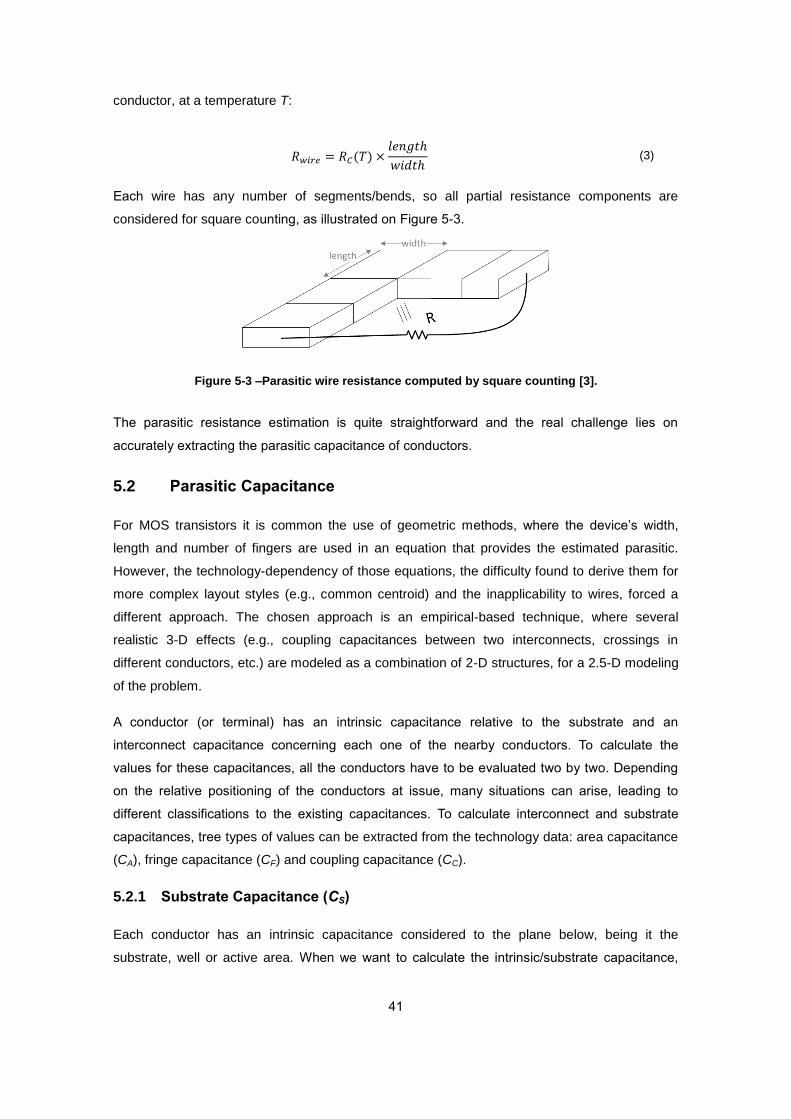
41
conductor, at a temperature T:
𝑅 = 𝑅 (𝑇) ×𝑙𝑒𝑛𝑔𝑡
𝑤𝑖𝑑𝑡 (3)
Each wire has any number of segments/bends, so all partial resistance components are
considered for square counting, as illustrated on Figure 5-3.
Figure 5-3 –Parasitic wire resistance computed by square counting [3].
The parasitic resistance estimation is quite straightforward and the real challenge lies on
accurately extracting the parasitic capacitance of conductors.
5.2 Parasitic Capacitance
For MOS transistors it is common the use of geometric methods, where the device’s width,
length and number of fingers are used in an equation that provides the estimated parasitic.
However, the technology-dependency of those equations, the difficulty found to derive them for
more complex layout styles (e.g., common centroid) and the inapplicability to wires, forced a
different approach. The chosen approach is an empirical-based technique, where several
realistic 3-D effects (e.g., coupling capacitances between two interconnects, crossings in
different conductors, etc.) are modeled as a combination of 2-D structures, for a 2.5-D modeling
of the problem.
A conductor (or terminal) has an intrinsic capacitance relative to the substrate and an
interconnect capacitance concerning each one of the nearby conductors. To calculate the
values for these capacitances, all the conductors have to be evaluated two by two. Depending
on the relative positioning of the conductors at issue, many situations can arise, leading to
different classifications to the existing capacitances. To calculate interconnect and substrate
capacitances, tree types of values can be extracted from the technology data: area capacitance
(CA), fringe capacitance (CF) and coupling capacitance (CC).
5.2.1 Substrate Capacitance (CS)
Each conductor has an intrinsic capacitance considered to the plane below, being it the
substrate, well or active area. When we want to calculate the intrinsic/substrate capacitance,

42
two types of capacitors can be differentiated: Area Capacitance (CA), which covers the
capacitances on the overlap area, right below the conductor, and Fringe Capacitance (CF) which
features all the other lines, as presented in Figure 5-4.
Figure 5-4 – Capacitances considered to compute substrate capacitance.
As referred, these capacitors and their characteristics relate to the electric field lines, so it
becomes obvious that the value of the capacitance will be greater where the density of field
lines is bigger, so in this case it’s expected that CA will have a greater capacitance value than
CF. This capacitance is computed by the sum of the area and the two fringe components (4).
𝐶 = (𝐶 (𝑤𝑖𝑑𝑡) × 𝑙𝑒𝑛𝑔𝑡) + (2 × 𝐶 (𝑠𝑝𝑎𝑐𝑒) × 𝑙𝑒𝑛𝑔𝑡) (4)
where the area capacitive component CA is obtained by interpolation of the technology-
dependent data provided in the foundry’s TDKs as a function of the conductor’s width, and then
computed over its length. The fringe component CF is obtained by interpolation but with the
space between the conductor and the closest shape in that same layer as a look-up variable.
5.2.2 Interconnect Capacitance (CI)
It is defined as interconnect the capacitance between two conductors on different layers or in
the same layer. To ensure that all shapes are evaluated and all capacitances covered, the tool
performs three assessments: interconnect amongst terminals, amongst wires and interconnect
between wires and terminals. The routing paths are chopped down into rectangular shapes and
the terminals are sort out into the various poly and metal1 shapes that define them. The
conductors are then evaluated two by two and the partial capacitances are summed up in the
end for each interconnect.
When the two conductors in question are in the same layer, as sketched in Figure 5-5, the
Fringe components refer to the lines that exist from top-to-top and from bottom-to-bottom of the
conductor stripes.

43
Figure 5-5 – Capacitances considered for interconnect capacitance on the same layer.
For the lines that go from side to side between the conductors, the capacitor is classified as
Coupling Capacitance (CC). Coupling capacitance is only present in this situation, because it
refers to lateral overlap of the stripes. In this situation the fringe components are scorned and
only Cc is considered:
𝐶 = (𝐶 (𝑐_𝑠𝑝𝑎𝑐𝑒) × 𝑝𝑎𝑟𝑎𝑙𝑙𝑒𝑙_𝑙𝑒𝑛𝑔𝑡) (5)
where Cc(c_space) is the coupling capacitive component obtained by the interpolation in
conductor’s c_space (space between conductors) of the foundry provided values, and
parallel_lenght is the length on which the two conductors laterally overlap.
If the conductors are in different layers the interconnect value depends on the area and fringe
components between the two conductors, as indicated in (6). In this case, two situations car
occur: Or the plates don’t vertically overlap and only fringe components (CF) are evaluated to
come up with the interconnect capacitance; or they overlap and an area component (CA)
appears. As before, the area capacitance refers to the area between the plates and its value
increases as the total overlap area increases. If the plates totally overlap, the value of the area
capacitance is maximum and only side-to-side components of the fringe capacitance are
present, which in most cases can be scorned.
𝐶 = (𝐶 ( 𝑒𝑟𝑙𝑎𝑝_𝑤𝑖𝑑𝑡) × 𝑝𝑎𝑟𝑎𝑙𝑙𝑒𝑙_𝑙𝑒𝑔𝑡) + (2 × 𝐶 (𝑠𝑝𝑎𝑐𝑒) × 𝑝𝑎𝑟𝑎𝑙𝑙𝑒𝑙_𝑙𝑒𝑛𝑔𝑡) (6)
For these distinct situations, different variables are considered. If the conductors overlap,
overlap_width is used as a look-up variable for CA component, as shown in Figure 5-6. The
fringe components CF are interpolated again with the space between the higher plate and the
closest shape in the same layer.
If the plates do not overlap the area component CA vanishes and only CF is considered to make
the computation, as illustrated in Figure 5-7. In this case the equation used is the same (6) but
only with the fringe part, and a new geometrical factor is deemed: c_space.

44
Figure 5-6 – Interconnect capacitance for overlapping plates (2D view).
Figure 5-7 – Interconnect capacitance for non-overlapping plates (3D view).
The decay of CF is approximately linear with the increase of space between conductors
although the rate of decay is different for each pair of materials, as presented in Figure 5-8.
Figure 5-8 – CF decay with respect to the space between conductors.

45
To address this decay a new factor has been added to the equation which is multiplied to the
provided value from the foundry. Although the value of CF doesn’t depend much on the higher
plate’s width as concluded before, it does decay with the lower plate’s width decrease. To see
just how much the value of width influences the variation in CF, a plate was placed at different
c_space values (0, 0.5, 1, 1.5,…) initially with an infinite value of width (plates separated by
more than 3µm are considered having no influence on each other, so if the lower plate has a
width of 3.5µm or an infinite width the results are the same), and then reduced iteratively to
observe the change. The results are illustrated on Figure 5-9.
Figure 5-9 – CF decay with respect to the lower plate’s width.
In this picture is clear that the decay is roughly the same for every value of space but 0. With
this in mind, a new decay factor that depends on the lower plate’s width has to be added with a
slope coefficient that is going to have only two possible values. The final equation to compute
the interconnect capacitance related to fringe components is presented next:
𝐶 = 2 × (𝐶 (𝑠𝑝𝑎𝑐𝑒) × (1 × 𝑐 ) × (𝑤 + 𝑤 × 𝑤𝑖𝑑𝑡)) × 𝑝𝑎𝑟𝑎𝑙𝑙𝑒𝑙_𝑙𝑒𝑛𝑔𝑡 (7)
where the green part corresponds to the decay due to the space between the conductors and
is fitted depending on the type of shapes in evaluation. The red part corresponds to width
related decay and w0 and w1 are fitted depending on which the space between the shapes is
zero or not. This formulation is not only applied to this particular situation but to every situation
where CF is considered, depending on the geometrical factors. Revisiting equation (4), if the
plate in not above active area or a well, it is considered that the substrate plate below is infinite
to every direction, so CF suffers no decay. Reviewing now equation (6), in that situation the

46
plate is either completely or partly below the other one so the plate is spitted in area and fringe
part. The fringe part is always at c_space = 0 so the decay is well defined and this equation can
be reformulated as in equation (8).
𝐶 = (𝐶 ( 𝑒𝑟𝑙𝑎𝑝 ) × 𝑝𝑎𝑟𝑎𝑙𝑙𝑒𝑙 ) +
(2 × 𝐶 (𝑠𝑝𝑎𝑐𝑒)(𝑤 + 𝑤 × 𝑤𝑖𝑑𝑡) × 𝑝𝑎𝑟𝑎𝑙𝑙𝑒𝑙_𝑙𝑒𝑛𝑔𝑡)
(8)
where w0 and w1 are fitted to the decrease of 0 space presented in Figure 5-9.
5.3 Geometrical considerations
To ensure the embedded tool approximates the values extracted by Mentor Graphics’ Calibre®,
a few more geometrical factors have to be taken into account. When two conductors are
evaluated, not only their geometrical characteristics are being considered, but also the physical
layout that surrounds them is being analyzed. For example to retreat the desired CF value from
the design kit tables the space between the conductor and the closest shape in that layer is
used as a look-up variable, as said before. Another crucial consideration is space occupation in
between the two conductors at issue, which is evaluated along the parallel_lenght area, as
illustrated in Figure 5-10.
S1
S2
parallel_length
x1
x2
Figure 5-10 – Top view example of space occupation analysis.

47
In this example the interconnect capacitance is oriented in a horizontal way from one plate to
the other, so the space occupation analysis is performed vertically. This geometrical module
evaluates the vertical opened space and generates a percentage (9) that is later multiplied by
the estimated interconnect capacitance.
( ) = ∑
𝑝𝑎𝑟𝑎𝑙𝑙𝑒𝑙_𝑙𝑒𝑛𝑔𝑡× 100 (9)
Actually this evaluation is made even before the capacitance estimation, so not only the values
for the interconnect capacitance are better fitted to the geometrical disposition, but also when
the parallel_length area is totally obstructed the percentage is immediately zero and the
parasitic estimation is not even executed.
AIDA-PEx has to work over a detailed routing as well as over the global routing created when
the extraction is taking place inside the optimization loop. This global routing, as said before,
doesn’t account for wire overlap or design rule break, so additional geometrical concerns have
to be made so that the extraction doesn’t crash.
When two routing paths overlap (the routing paths of the global router are all done in metal1
stripes), the best solution is to consider that in the final detailed layout one of them will be
sketched in metal2, so a random path of the two is chosen and upgraded to the layer above for
capacitance extraction purposes.
This is the solution for when the conductors overlap, but it can also happen that they don’t
overlap but run alongside each other at a distance smaller than the minimum permitted (or even
at zero distance which would join the nets together). In this case it is considered that the paths
are separated by the minimum distance allowed by the design rules.
5.4 Preliminary Tests
In this subsection, the intra-module capacitances (substrate and interconnect) are extracted in
AIDA-PEx and in Calibre® for a set of NMOS and PMOS transistors with different specifications,
to test the precision of the parasitic extraction inside the models, as presented in Table 5-1. It
was decided to conduct this preliminary study for the capacitances of the transistors’ terminals
due the influence they have in the final net capacitances, which is bigger than the routing wire
ones.
The error associated with interconnect capacitances doesn’t exceed 11% but the intrinsic one
reaches values of 39% of the intended value. Yet, the bigger values of relative error occur for
very small values of capacitances, values that are smaller than 1 fento Farad, so this error won’t
have a great influence on the performance of the circuit.

48
Table 5-1 – Intra-module Capacitance Comparison.
Module Terminal
AIDA Pex (fF) Calibre Pex (fF) Relative Error (%)
CS 1 Coup.
Net CI
2 CS
Coup. Net
CI CS CI
N-MOS l=30u w=0,2u nf=8
Source 0,243 Gate 1,372 0,192 Gate 1,425 +26,563 -3,719
Gate 1,589 Drain 1,331 1,76 Drain 1,363 -9,716 -2,348
Drain 0,099 Source 2,481 0,086 Source 2,397 +15,116 +3,504
P-MOS l=50u w=0,2u nf=4
Source 0,756 Gate 1,594 0,865 Gate 1,778 -12,601 -10,349
Gate 0,711 Drain 1,555 0,749 Drain 1,688 -5,073 -7,879
Drain 0,05 Source 3,854 0,037 Source 3,651 +35,135 +5,56
P-MOS l=100u w=0,2u nf=30
Source 0,502 Gate 4,915 0,653 Gate 4,984 -23,124 -1,384
Gate 5,196 Drain 4,877 6,553 Drain 4,913 -20,708 -0,733
Drain 0,37 Source 8,451 0,338 Source 8,323 +9,467 +1,538
1 – Substrate capacitance
2 – Interconnect capacitance
5.5 Conclusions
In this chapter, the methodology used by the proposed parasitic extractor was described, along
with the steps that led to the respective modeling. The equations considered in the model for the
estimated parasitic resistances and capacitances, along with the geometrical factors were
presented.
Avoiding the need for the detailed routing in the optimization process, the best quality of AIDA-
PEx is the possibility to work over a global routed layout, which largely accelerates the process
due to the difference of time that takes to get a simplistic global routing instead of a complete
detailed one.

49
Chapter 6 Results
In this chapter the experimental results of the proposed parasitic extractor for some example
circuits are presented.
The framework of the proposed methodology for the parasitic extractor of analog ICs layout,
based on foundry data and empirical models, has been coded in JAVA™. In both examples, the
experimental results are compared with Mentor Graphics Calibre® to validate the accuracy of
the approach. Also, when comparing results obtained with AIDA-PEx and Calibre®, it is
important to keep in mind that AIDA-PEx extractions were done over layouts with only global
routing, and, the ones in Calibre® were done over complete layouts with the detailed routing in
place.
6.1 Case Study I – Single Ended 2-Stage Amplifier
The first circuit used as test case is a single ended 2-stage amplifier. The amplifier schematic is
presented in Figure 6-1 (a) and was designed for UMC 130 nm CMOS technology. This circuit
was optimized for maximum gain and minimum area with AIDA layout-aware, resulting in the
Pareto optimal front (POF) of sizing solutions illustrated in Figure 6-1 (b).
VDD VDD VDD
OUT
IPIN
VSS VSS VSS
NRC
REF
N1
N2 N3
(a) Circuit Schematic (b) POF
Figure 6-1 – Single ended 2-stage amplifier used as respective POF.
From this POF two points were chosen with different layout dispositions, one of them with the
smallest area available and 51dB of gain and the other in the middle of the POF data line with
75dB of gain (Figure 6-1 (b)), to compare the estimated capacitances with the ones extracted by
Calibre®.

50
In Table 6-1 the results for the direct comparison between AIDA-PEx and Calibre® for the bulk
capacitance of both layout implementations are presented.
In this table it is clear that the error is higher in the second sizing, where the components have
bigger dimensions and consequently the routings have a higher contrast, so the circuit is more
susceptible to parasitic effects. For the interconnect capacitances between nets for the first
implementation, the results are presented on Table 6-2.
Table 6-1 – Direct Bulk Capacitance Comparison.
Layout Net REF D11 IP IN D12 D12R NETZ53 OUT
51dB
AIDA-PEx (fF) 6,945 1,873 0,455 0,436 1,2 1,477 0,638 1,716
Calibre (fF) 7,115 1,713 0,389 0,389 0,903 1,129 0,581 1,884
Absolut Error (fF)
-0,17 +0,159 +0,065 +0,047 +0,297 0,3477 +0,056 -0,168
Relative Error (%)
-2,39 +9,308 +16,79 +11,94 +32,93 +30,79 +9,624 -8,903
75dB
AIDA-PEx (fF) 15,956 5,262 3,391 3,394 2,444 1,906 2,145 3,103
Calibre (fF) 19,864 8,709 3,61 3,61 4,703 1,561 6,841 2,814
Absolut Error (fF)
-3,908 -3,447 -0,219 -0,216 -2,259 +0,345 -4,696 +0,289
Relative Error (%)
-19,67 -39,58 -6,066 -5,983 -48,03 +22,1 -68,64 +10,27
Table 6-2 – Direct Interconnect Capacitance Comparison for 51dB Layout.
Calibre®
NET REF N2 IP IN N3 NRC N1 VDD VSS OUT
AID
A-P
Ex
REF
0 0,03 0 0,238 0 0,355 3,414 0 2,372
N2 0,009
0,0407 0,2799 0,252 0 0,465 0,114 0,899 0
IP 0,026 0,097
0 0,222 0 0,261 0,052 0,001 0
IN 0 0,278 0,009
0 0 0,297 0,026 0 0
N3 0,172 0,266 0,2 0
0,011 0,486 0,229 0,722 0,268
NRC 0,002 0 0 0 0,018
0 0 0,002 0,021
N1 0,359 0,449 0,224 0,224 0,384 0
1,216 0 0
VDD 3,603 0,001 0,005 0 0,018 0,07 0,46
0,006 3,143
VSS 0,003 0,802 0,031 0,136 0,503 0 0,01 0,002
0,424
OUT 3,044 0 0 0 0,412 0,036 0,015 3,397 0,421
In this table the interconnect capacitances net-to-net are directly compared, and the larger
errors occur on the capacitances to the power nets. In Table 6-3 the same results are presented

51
to the 75dB sizing. Considering that the layouts used for the two extractors have slightly
different routing paths, the results are promising. Although there are still some cases where the
capacitances diverge, the extracted values show sufficient approximation for the global router.
Table 6-3 – Direct Interconnect Capacitance Comparison for 75dB Layout.
Calibre®
NET REF N2 IP IN N3 NRC N1 VDD VSS OUT
AID
A-P
Ex
REF
0,195 0 0 0,054 0,046 0,917 9,596 0,002 7,196
N2 0,464
0,155 2,255 1,363 0,006 0,892 1,159 1,928 0,003
IP 0,003 0,152
0 2,249 0 2,196 0,176 0,017 0
IN 0 2,547 0,029
0 0 2,209 0,191 0,018 0
N3 0,091 1,305 2,511 0
0,175 0,747 0,916 0,805 0,729
NRC 0,001 0,008 0 0 0,085
0 0 0 0,001
N1 0,905 2,098 2,585 2,562 1,64 0
2,159 0,011 0
VDD 9,407 0,011 0 0 0,004 0,049 0,384
0,594 0,908
VSS 0,022 1,38 0 0,028 0,775 0,013 0 0
0,911
OUT 7,938 0,003 0 0 0,819 0,288 0,008 2,143 1,045
As stated, this circuit was optimized for maximum gain and minimum area using AIDA, where
the resultant POF was illustrated in Figure 6-1(b). The results for the performance
measurements for these two implementations are presented in Table 6-4, where the netlist
resultant from the traditional simulation-based sizing is compared with the extracted netlists
from AIDA-PEx and Calibre®, resultant from the layout-aware optimization-based sizing.
Table 6-4 – Pre/Post-Layout Simulation.
Specs
51 dB 75dB
Traditional Layout-aware Traditional Layout-aware
Netlist Calibre® AIDA-PEx
Calibre® Netlist Calibre® AIDA-PEx
Calibre®
Gdc max ≥ 50 dB 53,7 53,7 50,9 50,9 75,4 75,4 74,6 74,6
Gbw ≥ 200 MHz 208.69 183,37* 204,29 206,30 206,68 182,66 209,25 210,05
Pm ≥55 º 55,56 46,42 74,27 73,54 57,83 58,27 64,51 60,56
Idd ≤ 200 µA 135,4 135,1 176,8 176,5 190,5 189,2 190,9 190,2
PSRR ≥ 55 dB 77,23 75,53 75,44 75,45 88,09 77,02 83,89 80,12
Voff ≤ 5 mV 3,8 3,83 4,39 4,39 4,83 4,91 5,02 4,38
No ≤ 600 µVrms 435,6 441,8 301,2 305,9 347,7 336,3 381,9 390,3
Sn ≤ 100 nV/√Hz 21,41 21,59 16,17 16,32 25,2 25,7 26,4 26,4
*Broken constraints

52
As it is clear in these tests, a small difference in certain capacitances (mostly referent to critical
nets of the circuit) represents a great discrepancy in the performance evaluation of the circuit.
The resulted POFs for the traditional simulation-based sizing and for the layout-aware synthesis
are presented in Figure 6-2, and in Table 6-5 and Table 6-6 the resultant layouts for are
portrayed, where the images are scaled for comparison purposes.
Figure 6-2 – Traditional and Layout-aware optimization POFs (Case Study I).
Table 6-5 – Illustration of resulted layouts for the 51dB circuit.
Optimization Layout Area [µm2]
GD
C 5
1 d
B
Traditional
337
Layout-aware
311
In the first case the area of the resultant layout-aware is smaller than the one obtained by the
traditional simulation-based sizing, but in the second case the layout-aware one is bigger. In
spite of these different sizings, the traditional sizing might not fulfill all the specifications after

53
layout because it doesn’t account for the physical effects as the layout-aware does. In the next
case study the importance of a layout-aware approach will be clearer.
Table 6-6 – Illustration of resulted layouts for 75dB circuit.
Optimization Layout Area [µm2]
GD
C 7
5d
B
Traditional
1021
Layout-aware
1330
6.2 Case Study II – 2-Stage Folded Cascode Amplifier
In the first case study the main goal was to directly compare the values for the capacitances
extracted by AIDA-PEx and Calibre®. In this second example, the goal is to demonstrate how a
layout-aware approach with accurate parasitic estimations can be valuable for a correct sizing
of the circuit that fulfills all the specifications. The circuit used in the optimization process is the
two-stage folded cascode amplifier of Figure 6-3, where the circuit was sized using the
traditional optimization-based process and a layout-aware optimization.
The results for the traditional and for the layout-aware optimization are presented in Table 6-7,
where the performances for the resulted layouts are simulated using the netlist extracted both
from AIDA-PEx and from Calibre®.
In the traditional simulation-based optimization the parasitic effects are not accounted for, and
for that reason, when the resulted layout is simulated with the inclusion of circuit’s parasitics, the
GBW specification is no longer met (whether the circuit is tested on Calibre® or on AIDA-PEx.

54
Vss
vb
vbnc
Vdd
MN31 MN32
MN21
MPB10
MPB8
MN22
MPB11
MPB9
XC0
out
vbn MN5
MP4
vbn
vbnc
vbp
MNB6
MNB5
MPB1
MPB2
MPB4
MPB3
vbn
vb
in ip
vbp
MP11 MP12
MPB10L=LB1W=WB1NF=4NR=2
L=LB2W=WB2NF=2NR=1
L=LB1W=WB1NF=NB1NR=NRB33
L=LB2W=WB2NF=NB2NR=1
L=L2W=W2NF=1NR=1
L=LB4W=WB4NF=1NR=1
L=LB1W=WB1NF=NB1NR=1
L=L1W=W1NF=N1NR=NR1
L=LB3W=WB3NF=NB3NR=NRB3
L=L2W=W2NF=N2NR=1
L=LB4W=WB4NF=NB4NR=1
L=LB4W=WB4NF=NB4NR=1
L=L2W=W2NF=N2NR=1
L=LB2W=WB2NF=NB22NR=2
L=LB3W=WB3NF=NB3NR=NRB3
L=LB2W=WB2NF=NB22NR=2
L=L3W=W3NF=N3NR=1
L=LB4W=WB4NF=NB5NR=NRB5
L=LCNF=NFCM=2
Figure 6-3 –2-stage folded cascode amplifier.
In the layout-aware sizing optimization, the circuit is wittingly over estimated so that when the
parasitic components are added the specifications are all fulfilled. In terms of consumption the
circuit needs a little more current, consequently increasing the frequency. However, the circuit is
correctly sized and the performance measurements from the AIDA-PEx netlist match the ones
from Calibre®.
Table 6-7 – Performance Comparison for the traditional and layout-aware optimizations.
Traditional Layout-Aware
Specs Netlist1
AIDA-PEx Calibre® AIDA-PEx Calibre®
Idd Min [mA] 5.35 5.62
Gbw ≥ 400 MHz 402.07 392.33 392.59 408.05 408.2
Gdc ≥ 70 dB 73.53 73.53 73.53 75.68 75.68
Area ≤ 20k µm2 12.09k 16.49k 16.34k
No ≤ 500 µVrms 197.05 195.37 194.93 195.48 195.16
Pm ≥55 º 57.97 55.54 55.26 57.04 56.78
Ov2
≥ 50 mV 59.48 59.48 59.48 50.61 50.48
D3
≥ 100 mV 100.33 105.06 105.06 105.37 105.06 1 - Performance for the netlist excluding parasitics.
2 - Overdrive voltage
3 – Saturation voltage
Here, the results have less error than in the previous case study because the circuit is larger
and the routing differences are less significant.
In Figure 6-4, both traditional simulation-based optimization and layout-aware synthesis POFs
are presented, where the circuit sizings that resulted from the traditional one were tested with
parasitic effects to evaluate the post-layout performance. From the resulted layouts, only one
held the fulfillment of all the specifications (represented by a circle O), and all the other sizings
became unfeasible, with one or more specifications not fulfilled (represented by a cross X). The
layout-aware POF, although obtaining layouts with a worse performance, guarantees the entire
specification fulfillment for all the resulted circuit sizings.

55
Figure 6-4 – Traditional and Layout-aware optimization POFs (Case Study II).
In Figure 6-5 the resulted layouts for the sizing used in Table 6-7 are illustrated. Although the
layouts are alike, the traditional one doesn’t fulfill the specifications as the layout-aware one
does, due to the inclusion of physical effects in the circuit sizing phase.
(a) Traditional Optimization (b) Layout-Aware Optimization
Figure 6-5 –Illustration of resulted layouts (Case Study II).
6.3 Conclusions
In this chapter, two test cases were addressed to show the capabilities of the tool. The first
example, a single ended 2-stage amplifier, was used to directly compare the AIDA-PEx
extraction results with a standard industry tool, Mentor Graphics Calibre®. The second example,

56
a 2-stage folded cascode amplifier, was used to demonstrate the importance of the layout-
aware synthesis to get a first-right implementation that fulfills all the specification even in the
presence of circuit’s parasitics.
The results in case study II are better than the previous one, because of the size of the circuit,
where the components are larger than the first one. In terms of circuit’s parasitics, these have a
bigger effect, and the parasitic components have larger values. However, the error between the
extracted values from AIDA-PEx and Calibre® are smaller because the difference in the layouts
extracted by these tools (routing paths) is less significant to the final parasitic extractions.

57
Chapter 7 Conclusions and Future Work
This chapter presents the closing remarks, and then, the future directions for the continuous
development of AIDA-PEx are outlined.
7.1 Conclusions
The proposed methodology for layout-aware analog IC sizing was proved by the implementation
of a tool, AIDA-PEx, that enables the layout generation block to retrieve the layout-related data
(geometrical characteristics, parasitic components, etc.) fast enough to have acceptable running
times. AIDA-PEx outstands from the remaining tools presented in the state-of-the-art (Chapter
2), addressing some drawbacks by obtaining a complete empirical based 2.5-D parasitic
extraction with approved results when compared to a commercial tool widely accepted in the
industry, Calibre®.
By merging the circuit optimizer with the layout generator (AIDA-C and AIDA-L), this layout
driven approach includes layout-related data in early stages of the optimization, with an
innovative solution for parasitic estimation of interconnect and substrate capacitance and global
routing in-loop for each different sizing solution. The lightweight built-in extractor estimates the
impact of layout parasitics for both floorplan and early-stages of routing without requiring a
detailed layout, greatly reducing overall evaluation time to in parasitic-aware optimization.
The tool relies on new regression on the technology related data retreated from the TDK, as
well as new computing and modeling of the interpolated data to accurately estimate the circuit’s
parasitics. Additionally, new geometrical factors are considered in the capacitance modeling,
which along with the formulations developed, result in an overall precision of the proposed
approach compared with already accepted tools.
In Chapter 6 two case studies were presented to validate the tool. In the first one, the results
showed sufficient accuracy for the proposed extractor, with errors below 40% for direct
capacitance comparison with Calibre®. In the second case study, the importance of the layout-
aware circuit sizing was verified, with almost 90% of the traditional optimization solutions turning
unfeasible after post-layout simulation. For this experiment, the results showed an outstanding
precision, with relative errors not exceeding 1%.
7.2 Future Work
The conducted experimental tests were presented for the UMC 0.13µm design process,
although the formulations for the estimation of circuits’ parasitics would also work for other
technologies, if the provided TDKs matched the desired technology. In the development of this

58
work only the UMC 0.13µm design kit was available, but for future reference the validation of
the modeling applied for other technologies would empower the tool.
In order to accelerate even more the extraction process, a solution of parallel computing could
be studied to be implemented in the tool. The extractor is fast, but for large circuits, if various
parts of the circuit could be analyzed at the same time, it would optimize the total runtime for an
even quicker estimation.
The frequency of operation of the circuits tested in this work rounds the hundreds of MHz. The
larger the value of the frequency, the more effect the parasitic components have in the final
circuit’s performance. The radio-frequency (RF) circuits can operate within a range of about
3kHz up to 300GHz, where if the parasitic effects are not accurately modeled, the estimated
performances will be different from the real ones, which can even lead to a total loss of the initial
constraints implied. The application of this extractor for RF circuits would challenge the
accuracy of the estimated and force the tool to be more robust.
AIDA-PEx project is not closed, far from it, this work served to validate the concept and it
provides support for further developments. New people will bring new insights in the analog IC
layout generation problem, and it is hoped that AIDA will converge to an application suitable for
industrial uses.

59
Chapter 8 References
[1] G. G. E. Gielen, “CAD tools for embedded analogue circuits in mixed-signal integrated
systems on chip,” IEEE Proceedings on Computers and Digital Techniques, vol. 152, no. 3,
pp. 317 – 332, May 2005.
[2] International Technology Roadmap for Semiconductors. (2012) ITRS 2012 Update.
[Online]. http://www.itrs.net/Links/2012ITRS/Home2012.htm.
[3] N. Lourenço, R. Martins and N. Horta, “Layout-Aware Sizing of Analog ICs using Floorplan
& Routing Estimates for Parasitic Extraction,” in DATE Conference and Exhibition, March
2015.
[4] “Mentor Graphics,” [Online] http://www.mentor.com.
[5] P. Vancorenland, G. Van der Plas, M. Steyaert, G. Gielen, and W. Sansen, “A layout-aware
synthesis methodology for RF circuits,” in Proc. IEEE/ACM ICCAD, pp. 358–362,
November 2001.
[6] M. Ranjan, et. al., “Fast, layout-inclusive analog circuit synthesis using pre-compiled
parasitic-aware symbolic performance models,” in DATE Conference and Exhibition,
pp.604-609, February 2004.
[7] A. Pradhan and R. Vemuri, “Efficient Synthesis of a Uniformly Spread Layout Aware Pareto
Surface for Analog Circuits,” in International Conference on VLSI Design, pp. 131-136,
January 2009.
[8] S. Youssef, F. Javid, D. Dupuis, R. Iskander, and M-M. Louerat, “A Python-Based Layout-
Aware Analog Design Methodology For Nanometric Technologies,” IEEE 6th Int. IDT, pp.
62-67, December 2011.
[9] H. Habal and H. Graeb, “Constraint-Based Layout-Driven Sizing of Analog Circuits,” IEEE
TCAD, vol. 30, no. 8, pp. 1089-1102, August 2011.
[10] M. Strasser, M. Eick, H. Gräb, U. Schlichtmann, and F. M. Johannes, “Deterministic analog
circuit placement using hierarchically bounded enumeration and enhanced shape
functions,” in IEEE/ACM International Conference on Computer-Aided Design (ICCAD), pp.
306-313, Nov. 2008.
[11] R. Castro-Lopez, O. Guerra, E. Roca and F. Fernandez, “An Integrated Layout-Synthesis
Approach for Analog ICs,” IEEE TCAD, vol. 27, no. 7, pp. 1179-1189, July 2008.

60
[12] A. Toro-Frias, R. Castro-Lopez, and F. Fernandez, “An automated layout-aware design
flow,” in Int. Conf. SMACD, pp. 73–76, September 2012.
[13] Y.-C. Liao, Y.-L. Chen, X.-T. Cai, C.-N. J. Liu and T.-C. Chen, “LASER – Layout-aware
Analog Synthesis Environment on Laker,”GLSVLSI’13, pp. 107-112, May 2013.
[14] W. H. Kao, C.-Y. Lo, M. Basel and R. Singh, “Parasitic Extraction: Current State of the Art
and Future Trends,” Proc. IEEE, vol. 89, no. 5, pp. 729-739, May 2001.
[15] A. Bansal, B. C. Paul and K. Roy, “An Analytical Fringe Capacitance Model for
Interconnects Using Conformal Mapping,” IEEE TCAD, vol.25, no. 12, pp. 2765-2774,
December 2006.
[16] G. Shomalnasab, H. Heys, and L. Zhang, “Analytic Modeling of Interconnect Capacitance
in Submicron and Nanometer Technologies,” IEEE International Symposium on Circuits
and Systems (ISCAS), pp. 2553-2556, May 2013.
[17] R. Sharma, V. K. Sehgal and D. S. Chauhan, “Closed-form Expressions for Extraction of
Capacitances in Multilayer VLSI Interconnects,” TENCON, pp. 1-4, November 2008.
[18] W. Gong, W. Yu, Y. Lu, Q. Tang, Q. Zhou and Y. Cai, “A Parasitic Extraction Method of VLSI
Interconnects for Pre-Route Timing Analysis,” ICCCAS, pp. 871-875, July 2010
[19] H. Foo, K. Leong and R. Mohd-Mokhtar, “Density Aware Interconnect Parasitic Estimation
for Mixed Signal Design,” ICCAS, pp. 258-262, October 2012.
[20] A. Agarwal, H. Sampath, V. Yelamanchili and R. Vemuri, “Fast and Accurate Parasitic
Capacitance Models for Layout-Aware Synthesis of Analog Circuits,” DAC, pp. 145-150,
June 2004.
[21] H. Yang and R. Vemuri, “Efficient Symbolic Sensitivity based Parasitic-Inclusive
Optimization in Layout Aware Analog Circuit Synthesis,” VLSID’07, pp. 201-206, January
2007.
[22] N. Karsilayan, J. Falbo and D. Petranovic, “Efficient and Accurate RIE Modeling
Methodology for BEOL 2.5D Parasitic Extraction,” MWSCAS, pp. 519-522, August 2014.
[23] “Maxwell’s Equations,” [Online]. http://hyperphysics.phy-astr.gsu.edu/hbase/electric/maxeq.
Html.
[24] “ANSYS,” http://www.ansys.com.
[25] “MIT – Massachusetts Institute of Technology,” http://web.mit.edu.

61
[26] “Synopsis," http://www.synopsys.com.
[27] "Cadence Design Systems Inc," http://www.cadence.com.
[28] “EMCoS,” http://www.emcos.com.
[29] “AIDAsoft,” http://www.aidasoft.com.
[30] R. Martins, N. Lourenco, A. Canelas, and N. Horta, “Electromigration-Aware and IR-Drop
Avoidance Routing in Analog Multiport Terminal Structures”, Design, Automation & Test in
Europe, pp. 1 – 6, March 2014.
[31] N. Lourenço, R. Martins, A. Canelas and N. Horta, “Floorplan-Aware Analog IC Sizing and
Optimization Based on Topological Constraints,” Integration, the VLSI journal, vol. 48,
January 2015.
[32] R. Martins, N. Lourenço, and N. Horta, "LAYGEN II ̶ Automatic Layout Generation of
Analog Integrated Circuits," IEEE TCAD, 32, pp.1641 – 1654, November 2013.