Embed Size (px)
Citation preview

8/14/2019 AHB Compatible DDR SDRAM Controller IP Core for ARM BASED SOC
http://slidepdf.com/reader/full/ahb-compatible-ddr-sdram-controller-ip-core-for-arm-based-soc 1/9
AHB Compatible DDR SDRAM Controller IP Core
for ARM BASED SOC1Dr.R.Shashikumar,
2C.N. Vijay Kumar,
3M.Nagendrakumar,
4C.S.Hemanthkumar
Professor Asst.prof Asst.Prof Sr.Lecturer
ECE dept, SJCIT, Chikkaballapur, Karnataka, India JVIT, Bidadi,
Abstract — DDR SDRAM is similar in function to the regular
SDRAM but doubles the bandwidth of the memory by
transferring data on both edges of the clock cycles.DDR
SDRAM most commonly used in various embedded application
like networking, image/video processing, Laptops ete. Now a
day’s many applications needs more and more cheap and fast
memory. Especially in the field of signal processing, requires
significant amount of memory. The most used type of dynamic
memory for that purpose is DDR SDRAM. For FPGA design
the IC manufacturers are providing commercial memory
controller IP cores working only on their products. Main
disadvantage is the lack of memory access optimization for
random memory access patterns. The ‘data path’ part of those
controllers can be used free of charge. This work propose an
architecture of a DDR SDRAM controller, which takes
advantage of those available and well tested data paths and can
be used for any FPGA device or ASIC design.[5]. In most of the
SOC design, DDR SDRAM is commonly used. ARM processor
is widely used in SOC’s; so that we focused to implement AHB
compatible DDR SDRAM controller suitable for ARM based
SOC design.
Keywords-AHB; DDR SDRAM; Verilog;IP core;
1 INTRODUCTIONThe DDR SDRAM is a high-speed CMOS, dynamic
random-access memory. It is internally configured as a quad
bank DRAM. The DDR SDRAM uses double data rate
architecture to achieve high-speed operation. The double data
rate architecture is essentially 2nprefetch architecture with an
interface designed to transfer two data words per clock cycle
at the I/O pins. A single read or write access for the DDR
SDRAM effectively consists of a single 2n-bit wide, one-
clock-cycle data transfer at the internal DRAM core and twocorresponding n-bit wide, one-half clock-cycle data transfers
at the I/O pins. A bidirectional data strobe (DQS) is
transmitted externally, along with data, for use in data
capture at the receiver. DQS is a strobe transmitted by theDDR SDRAM during READs and by the memory controller
during WRITEs. DQS is edge-aligned with data for READsand center-aligned with data for WRITEs.
Read and write accesses to the DDR SDRAM are
burst oriented; accesses start at a selected location and
continue for a programmed number of locations in a programmed sequence. Accesses begin with the registration
of an ACTIVE command, which is then followed by a READ
or WRITE command. The address bits registered coincident
with the ACTIVE command are used to select the bank and
row to be accessed. The address bits registered coincident
with the READ or WRITE command are used to select the
bank and the starting column location for the burst access.
The DDR SDRAM provides for programmable
READ or WRITE burst lengths of 2, 4, or 8 locations. An
auto precharge function may be enabled to provide a self
timed row precharge that is initiated at the end of the burst
access This model has implemented in RTL by Verilog. The
focus of this work is to implement behavioral model of DDR
SDRAM and also implemented on the Xilinx Spartan series
FPGA.The Top level model is as shown in Fig.1. The core
contains mainly two parts, AHB Slave and DDR SDRAM
controller.
Figure .1 Top Module
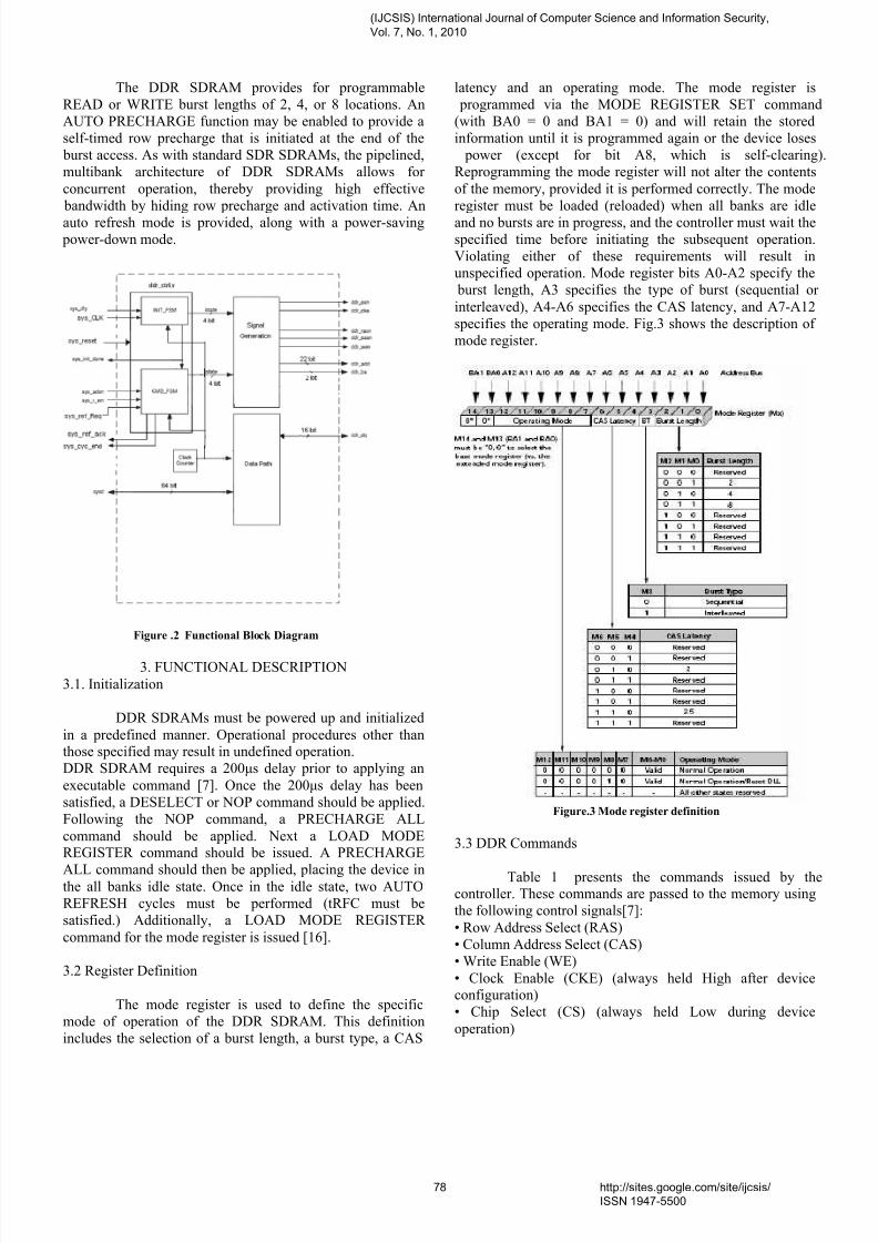
2. FUNCTIONAL BLOCK DIAGRAM
The functional block diagram of the DDR controller is shown
in Fig.2. It consists of four modules, AHB Salve, the main
control module, the signal generation module and the data
path module. The AHB slave normally connected to the AHB
bus Arbiter in the design. AHB master sends data to the AHB
slave based on that protocol. Burst mode read and writes andsplit transaction read and writes transactions supported. AHB
slave complies with the processor interface protocol of ARM
processor. The main control module has two state machines
and a refresh counter, which generates proper istate and
cstate outputs according to the system interface control
signals. The signal generation module generates the addressand command signals required for DDR based on istate and
cstate. The data path module performs the data latching and
dispatching of the data between the Processor and DDR.
Controller
Module
Data path
Module
Signal
Module
AHB
S
LAV
E
DDR
SDRAM
TOP MODULE
(IJCSIS) International Journal of Computer Science and Information Security,
Vol. 7, No. 1, 2010
77 http://sites.google.com/site/ijcsis/
ISSN 1947-5500
8/14/2019 AHB Compatible DDR SDRAM Controller IP Core for ARM BASED SOC
http://slidepdf.com/reader/full/ahb-compatible-ddr-sdram-controller-ip-core-for-arm-based-soc 2/9
The DDR SDRAM provides for programmable
READ or WRITE burst lengths of 2, 4, or 8 locations. An
AUTO PRECHARGE function may be enabled to provide a
self-timed row precharge that is initiated at the end of the
burst access. As with standard SDR SDRAMs, the pipelined,
multibank architecture of DDR SDRAMs allows for
concurrent operation, thereby providing high effective
bandwidth by hiding row precharge and activation time. An
auto refresh mode is provided, along with a power-saving power-down mode.
Figure .2 Functional Block Diagram
3. FUNCTIONAL DESCRIPTION
3.1. Initialization
DDR SDRAMs must be powered up and initialized
in a predefined manner. Operational procedures other thanthose specified may result in undefined operation.
DDR SDRAM requires a 200µs delay prior to applying an
executable command [7]. Once the 200µs delay has been
satisfied, a DESELECT or NOP command should be applied.
Following the NOP command, a PRECHARGE ALL
command should be applied. Next a LOAD MODEREGISTER command should be issued. A PRECHARGE
ALL command should then be applied, placing the device inthe all banks idle state. Once in the idle state, two AUTO
REFRESH cycles must be performed (tRFC must be
satisfied.) Additionally, a LOAD MODE REGISTER
command for the mode register is issued [16].
3.2 Register Definition
The mode register is used to define the specific
mode of operation of the DDR SDRAM. This definition
includes the selection of a burst length, a burst type, a CAS
latency and an operating mode. The mode register is
programmed via the MODE REGISTER SET command
(with BA0 = 0 and BA1 = 0) and will retain the stored
information until it is programmed again or the device loses
power (except for bit A8, which is self-clearing).
Reprogramming the mode register will not alter the contents
of the memory, provided it is performed correctly. The mode
register must be loaded (reloaded) when all banks are idle
and no bursts are in progress, and the controller must wait thespecified time before initiating the subsequent operation.
Violating either of these requirements will result in
unspecified operation. Mode register bits A0-A2 specify the
burst length, A3 specifies the type of burst (sequential or
interleaved), A4-A6 specifies the CAS latency, and A7-A12
specifies the operating mode. Fig.3 shows the description of
mode register.
Figure.3 Mode register definition
3.3 DDR Commands
Table 1 presents the commands issued by thecontroller. These commands are passed to the memory using
the following control signals[7]:
• Row Address Select (RAS)
• Column Address Select (CAS)
• Write Enable (WE)
• Clock Enable (CKE) (always held High after deviceconfiguration)
• Chip Select (CS) (always held Low during device
operation)
(IJCSIS) International Journal of Computer Science and Information Security,
Vol. 7, No. 1, 2010
78 http://sites.google.com/site/ijcsis/
ISSN 1947-5500

8/14/2019 AHB Compatible DDR SDRAM Controller IP Core for ARM BASED SOC
http://slidepdf.com/reader/full/ahb-compatible-ddr-sdram-controller-ip-core-for-arm-based-soc 3/9
Table 1 DDR SDRAM Commands
3.3.1 Command Functions
The fallowing commands are used in DDR SDRAM
controller core.
• Mode Register :
The Mode register is used to define the specificmode of DDR SDRAM operation, including the selection of
burst length, burst type, CAS latency, and operating mode.• Auto Refresh :
The REFRESH command instructs the controller to
perform an AUTO REFRESH command to the SDRAM. The
controller will acknowledge the REFRESH command withACK. DDR SDRAM is somewhat similar to regular
SDRAM. Both will break the RAM into smaller chunks for
simultaneous, synchronized request-and-reply access. In
addition, both types of memory can be packaged in DIMM
modules. However, DDR SDRAM will perform thealternating request-and-reply rhythm on both the rise and fall
of the clock cycle. This method effectively doubles the
bandwidth available and increases the speed the system can
access data in memory• Precharge:
The PRECHARGE command is used to deactivatethe open row in a particular bank. The bank is available for
subsequent row activation for a specified time (tRP) after the
PRECHARGE command is issued. Input A10 determines
whether one or all banks are precharged.
• ACTIVE Command:
The ACTIVE command activates a row in a bank,
allowing any READ or WRITE commands to be issued to a
bank in the memory array. After a row has been opened,
READ or WRITE commands can be issued to that row,
subject to the tRCD specification. When the controller
detects an incoming address that refers to a row in a bank other than the currently opened row, the controller issues an
address conflict signal. A PRECHARGE command is also
issued by the controller to deactivate the open row. The
controller also issues another ACTIVE command to the new
row.
• READ Command:
The READ command is used to initiate a burst read
access to an active row. The value on BA0 and BA1 selects
the bank address. The address inputs provided on A0 – Ai
select the starting column location. After the read burst is
over, the row is still available for subsequent access until it is
precharged.
• WRITE Command:
The WRITE command is used to initiate a burst
access to an active row. The value on BA0 and BA1 selects
the bank address, while the value on address inputs A0 – Ai
selects the starting column location in the active row. The
value of Write Latency is equal to one clock cycle.
4 .DDR SDRAM Controller Block
The controller block mainly consists of two FSMs
• Initial FSM
• Command FSM
It generates the required commands for initializingthe DDR SDRAM. The block diagram for the DDR SDRAM
controller is as shown in Fig.4.
Figure 4 Block Diagram of Controller Block
4.1 DDR SDRAM Initial FSM
Before normal memory accesses can be performed,
DDR needs to be initialized by a sequence of commands. The
INIT_FSM state machine handles this initialization. Fig.5
shows the state diagram of the INIT_FSM state machine.During reset, the INIT_FSM is forced to the i_IDLE state.
After reset, the sys_dly_200US signal will be sampled to
determine if the 200µs power/clock stabilization delay is
completed. After the power/clock stabilization is complete,
the DDR initialization sequence will begin and the
INIT_FSM will switch from i_IDLE to i_NOP state and inthe next clock to I_PRE.
The initialization starts with the PRECHARGE ALL
command. Next a LOAD MODE REGISTER command will be applied for the extended mode register to enable the DLL
inside DDR, followed by another LOAD MODE REGISTER
command to the mode register to reset the DLL. Then aPRECHAGE command will be applied to make all banks in
the device to idle state. Then two, AUTO REFRESH
commands, and then the LOAD MODE REGISTER
command to configure DDR to a specific mode of operation.
After issuing the LOAD MODE REGISTER command and
the tMRD timing delay is satisfied, INIT_FSM goes toi_ready state and remains there for the normal memory
(IJCSIS) International Journal of Computer Science and Information Security,
Vol. 7, No. 1, 2010
79 http://sites.google.com/site/ijcsis/
ISSN 1947-5500
8/14/2019 AHB Compatible DDR SDRAM Controller IP Core for ARM BASED SOC
http://slidepdf.com/reader/full/ahb-compatible-ddr-sdram-controller-ip-core-for-arm-based-soc 4/9
access cycles unless reset is asserted. Also, signal
sys_init_done is set to high to indicate the DDR initialization
is completed. The i_PRE, i_AR1, i_AR2, i_EMRS and
i_MRS states are used for issuing DDR commands. The
LOAD MODE REGISTER command configures the DDR by
loading data into the mode register through the address bus.
The data present on the address bus (ddr_add) during the
LOAD MODE REGISTER command is loaded to the mode
register. The mode register contents specify the burst length, burst type, CAS latency, etc. A PRECHARGE/AUTO
PRECHARGE command moves all banks to idle state. As
long as all banks of the DDR are in idle state, mode register
can be reloaded with different value thereby changing the
mode of operation. However, in most applications the mode
register value will not be changed after initialization. This
design assumes the mode register stays the same after
initialization.
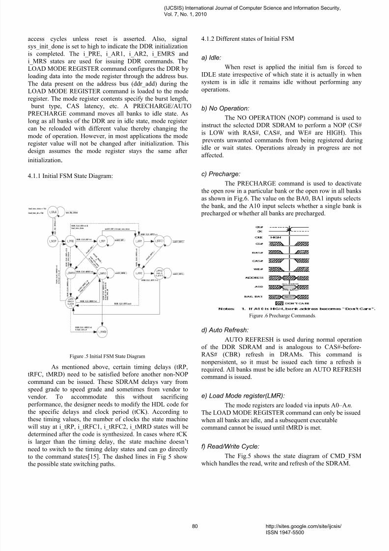
4.1.1 Initial FSM State Diagram:
Figure .5 Initial FSM State Diagram
As mentioned above, certain timing delays (tRP,tRFC, tMRD) need to be satisfied before another non-NOP
command can be issued. These SDRAM delays vary from
speed grade to speed grade and sometimes from vendor to
vendor. To accommodate this without sacrificing
performance, the designer needs to modify the HDL code for
the specific delays and clock period (tCK). According tothese timing values, the number of clocks the state machine
will stay at i_tRP, i_tRFC1, i_tRFC2, i_tMRD states will be
determined after the code is synthesized. In cases where tCK
is larger than the timing delay, the state machine doesn’t
need to switch to the timing delay states and can go directly
to the command states[15]. The dashed lines in Fig 5 showthe possible state switching paths.
4.1.2 Different states of Initial FSM
a) Idle:
When reset is applied the initial fsm is forced to
IDLE state irrespective of which state it is actually in when
system is in idle it remains idle without performing any
operations.
b) No Operation:
The NO OPERATION (NOP) command is used to
instruct the selected DDR SDRAM to perform a NOP (CS#
is LOW with RAS#, CAS#, and WE# are HIGH). This
prevents unwanted commands from being registered during
idle or wait states. Operations already in progress are not
affected.
c) Precharge:
The PRECHARGE command is used to deactivate
the open row in a particular bank or the open row in all banksas shown in Fig.6. The value on the BA0, BA1 inputs selects
the bank, and the A10 input selects whether a single bank is precharged or whether all banks are precharged.
Figure .6 Precharge Commands.
d) Auto Refresh:
AUTO REFRESH is used during normal operation
of the DDR SDRAM and is analogous to CAS#-before-
RAS# (CBR) refresh in DRAMs. This command is
nonpersistent, so it must be issued each time a refresh is
required. All banks must be idle before an AUTO REFRESHcommand is issued.
e) Load Mode register(LMR):
The mode registers are loaded via inputs A0–An.
The LOAD MODE REGISTER command can only be issued
when all banks are idle, and a subsequent executable
command cannot be issued until tMRD is met.
f) Read/Write Cycle:
The Fig.5 shows the state diagram of CMD_FSM
which handles the read, write and refresh of the SDRAM.
(IJCSIS) International Journal of Computer Science and Information Security,
Vol. 7, No. 1, 2010
80 http://sites.google.com/site/ijcsis/
ISSN 1947-5500
8/14/2019 AHB Compatible DDR SDRAM Controller IP Core for ARM BASED SOC
http://slidepdf.com/reader/full/ahb-compatible-ddr-sdram-controller-ip-core-for-arm-based-soc 5/9
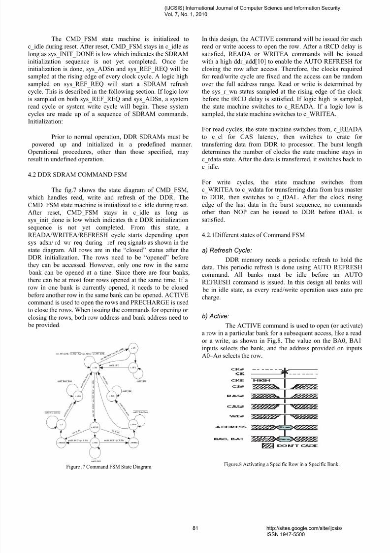
The CMD_FSM state machine is initialized to
c_idle during reset. After reset, CMD_FSM stays in c_idle as
long as sys_INIT_DONE is low which indicates the SDRAM
initialization sequence is not yet completed. Once the
initialization is done, sys_ADSn and sys_REF_REQ will be
sampled at the rising edge of every clock cycle. A logic high
sampled on sys_REF_REQ will start a SDRAM refresh
cycle. This is described in the following section. If logic low
is sampled on both sys_REF_REQ and sys_ADSn, a systemread cycle or system write cycle will begin. These system
cycles are made up of a sequence of SDRAM commands.
Initialization:
Prior to normal operation, DDR SDRAMs must be
powered up and initialized in a predefined manner.
Operational procedures, other than those specified, mayresult in undefined operation.
4.2 DDR SDRAM COMMAND FSM
The fig.7 shows the state diagram of CMD_FSM,
which handles read, write and refresh of the DDR. The
CMD_FSM state machine is initialized to c_idle during reset.
After reset, CMD_FSM stays in c_idle as long assys_init_done is low which indicates th e DDR initialization
sequence is not yet completed. From this state, a
READA/WRITEA/REFRESH cycle starts depending upon
sys_adsn/ rd_wr_req_during_ ref_req signals as shown in the
state diagram. All rows are in the “closed” status after theDDR initialization. The rows need to be “opened” before
they can be accessed. However, only one row in the same
bank can be opened at a time. Since there are four banks,
there can be at most four rows opened at the same time. If a
row in one bank is currently opened, it needs to be closed before another row in the same bank can be opened. ACTIVEcommand is used to open the rows and PRECHARGE is used
to close the rows. When issuing the commands for opening or
closing the rows, both row address and bank address need to
be provided.
Figure .7 Command FSM State Diagram
In this design, the ACTIVE command will be issued for each
read or write access to open the row. After a tRCD delay is
satisfied, READA or WRITEA commands will be issued
with a high ddr_add[10] to enable the AUTO REFRESH for
closing the row after access. Therefore, the clocks required
for read/write cycle are fixed and the access can be random
over the full address range. Read or write is determined by
the sys_r_wn status sampled at the rising edge of the clock
before the tRCD delay is satisfied. If logic high is sampled,the state machine switches to c_READA. If a logic low is
sampled, the state machine switches to c_WRITEA.
For read cycles, the state machine switches from, c_READA
to c_cl for CAS latency, then switches to crate for
transferring data from DDR to processor. The burst length
determines the number of clocks the state machine stays inc_rdata state. After the data is transferred, it switches back to
c_idle.
For write cycles, the state machine switches from
c_WRITEA to c_wdata for transferring data from bus master
to DDR, then switches to c_tDAL. After the clock rising
edge of the last data in the burst sequence, no commandsother than NOP can be issued to DDR before tDAL is
satisfied.
4.2.1Different states of Command FSM
a) Refresh Cycle:
DDR memory needs a periodic refresh to hold the
data. This periodic refresh is done using AUTO REFRESH
command. All banks must be idle before an AUTO
REFRESH command is issued. In this design all banks will
be in idle state, as every read/write operation uses auto precharge.
b) Active:
The ACTIVE command is used to open (or activate)
a row in a particular bank for a subsequent access, like a read
or a write, as shown in Fig.8. The value on the BA0, BA1
inputs selects the bank, and the address provided on inputs
A0–An selects the row.
Figure.8 Activating a Specific Row in a Specific Bank.
(IJCSIS) International Journal of Computer Science and Information Security,
Vol. 7, No. 1, 2010
81 http://sites.google.com/site/ijcsis/
ISSN 1947-5500
8/14/2019 AHB Compatible DDR SDRAM Controller IP Core for ARM BASED SOC
http://slidepdf.com/reader/full/ahb-compatible-ddr-sdram-controller-ip-core-for-arm-based-soc 6/9
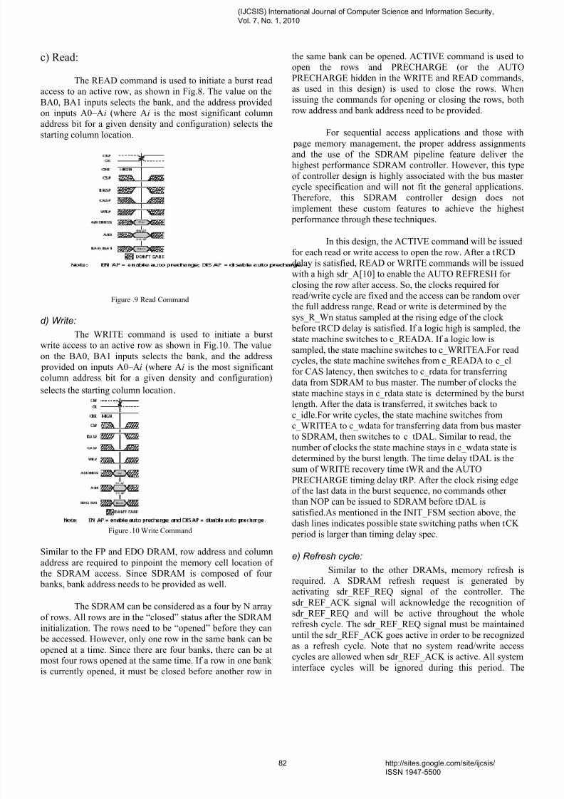
c) Read:
The READ command is used to initiate a burst read
access to an active row, as shown in Fig.8. The value on the
BA0, BA1 inputs selects the bank, and the address providedon inputs A0–Ai (where Ai is the most significant column
address bit for a given density and configuration) selects the
starting column location.
Figure .9 Read Command
d) Write:
The WRITE command is used to initiate a burst
write access to an active row as shown in Fig.10. The value
on the BA0, BA1 inputs selects the bank, and the address
provided on inputs A0–Ai (where Ai is the most significant
column address bit for a given density and configuration)
selects the starting column location.
Figure .10 Write Command
Similar to the FP and EDO DRAM, row address and column
address are required to pinpoint the memory cell location of the SDRAM access. Since SDRAM is composed of four
banks, bank address needs to be provided as well.
The SDRAM can be considered as a four by N array
of rows. All rows are in the “closed” status after the SDRAM
initialization. The rows need to be “opened” before they can
be accessed. However, only one row in the same bank can be
opened at a time. Since there are four banks, there can be atmost four rows opened at the same time. If a row in one bank
is currently opened, it must be closed before another row in
the same bank can be opened. ACTIVE command is used to
open the rows and PRECHARGE (or the AUTO
PRECHARGE hidden in the WRITE and READ commands,
as used in this design) is used to close the rows. When
issuing the commands for opening or closing the rows, both
row address and bank address need to be provided.
For sequential access applications and those with
page memory management, the proper address assignments
and the use of the SDRAM pipeline feature deliver thehighest performance SDRAM controller. However, this type
of controller design is highly associated with the bus master
cycle specification and will not fit the general applications.
Therefore, this SDRAM controller design does not
implement these custom features to achieve the highest
performance through these techniques.
In this design, the ACTIVE command will be issued
for each read or write access to open the row. After a tRCD
delay is satisfied, READ or WRITE commands will be issued
with a high sdr_A[10] to enable the AUTO REFRESH for
closing the row after access. So, the clocks required for read/write cycle are fixed and the access can be random over the full address range. Read or write is determined by the
sys_R_Wn status sampled at the rising edge of the clock
before tRCD delay is satisfied. If a logic high is sampled, the
state machine switches to c_READA. If a logic low is
sampled, the state machine switches to c_WRITEA.For readcycles, the state machine switches from c_READA to c_cl
for CAS latency, then switches to c_rdata for transferring
data from SDRAM to bus master. The number of clocks the
state machine stays in c_rdata state is determined by the burst
length. After the data is transferred, it switches back to
c_idle.For write cycles, the state machine switches fromc_WRITEA to c_wdata for transferring data from bus master
to SDRAM, then switches to c_tDAL. Similar to read, the
number of clocks the state machine stays in c_wdata state is
determined by the burst length. The time delay tDAL is the
sum of WRITE recovery time tWR and the AUTO
PRECHARGE timing delay tRP. After the clock rising edgeof the last data in the burst sequence, no commands other
than NOP can be issued to SDRAM before tDAL is
satisfied.As mentioned in the INIT_FSM section above, the
dash lines indicates possible state switching paths when tCK
period is larger than timing delay spec.
e) Refresh cycle:Similar to the other DRAMs, memory refresh is
required. A SDRAM refresh request is generated by
activating sdr_REF_REQ signal of the controller. The
sdr_REF_ACK signal will acknowledge the recognition of
sdr_REF_REQ and will be active throughout the wholerefresh cycle. The sdr_REF_REQ signal must be maintained
until the sdr_REF_ACK goes active in order to be recognized
as a refresh cycle. Note that no system read/write access
cycles are allowed when sdr_REF_ACK is active. All system
interface cycles will be ignored during this period. The
(IJCSIS) International Journal of Computer Science and Information Security,
Vol. 7, No. 1, 2010
82 http://sites.google.com/site/ijcsis/
ISSN 1947-5500
8/14/2019 AHB Compatible DDR SDRAM Controller IP Core for ARM BASED SOC
http://slidepdf.com/reader/full/ahb-compatible-ddr-sdram-controller-ip-core-for-arm-based-soc 7/9
sdr_REF_REQ signal assertion needs to be removed upon
receipt of sdr_REF_ACK acknowledge, otherwise another
refresh cycle will again be performed.
Upon receipt of sdr_REF_REQ assertion, the state
machine CMD_FSM enters the c_AR state to issue an AUTO
REFRESH command to the SDRAM. After tRFC time delay
is satisfied, CMD_FSM returns to c_idle.
5. DATA PATH
The fig.11 shows the data path module with inputs
and outputs as shown in the figure
Figure .11.Data Path Module.
The data flow design between the SDRAM and the
system interface. The module in this reference design
interfaces between the SDRAM with 16-bit bidirectional data
bus and the bus master with 64-bit bidirectional data bus. The
user should be able to modify this module to customize to fithis/her system bus requirements. The data path module
performs the data latching and dispatching of the data
between the processor and DDR.
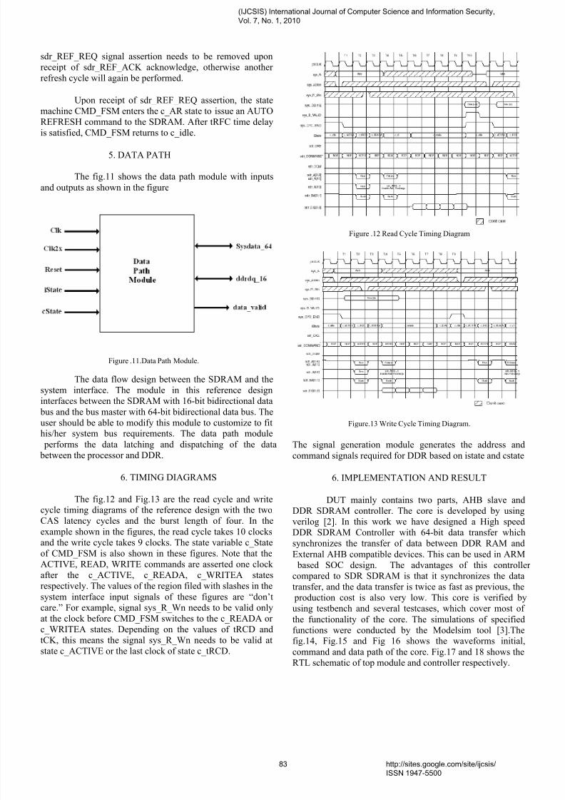
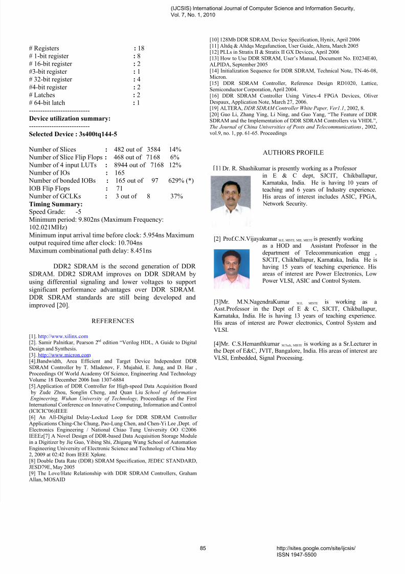
6. TIMING DIAGRAMS
The fig.12 and Fig.13 are the read cycle and writecycle timing diagrams of the reference design with the two
CAS latency cycles and the burst length of four. In the
example shown in the figures, the read cycle takes 10 clocks
and the write cycle takes 9 clocks. The state variable c_State
of CMD_FSM is also shown in these figures. Note that the
ACTIVE, READ, WRITE commands are asserted one clock after the c_ACTIVE, c_READA, c_WRITEA states
respectively. The values of the region filed with slashes in the
system interface input signals of these figures are “don’t
care.” For example, signal sys_R_Wn needs to be valid only
at the clock before CMD_FSM switches to the c_READA or
c_WRITEA states. Depending on the values of tRCD and
tCK, this means the signal sys_R_Wn needs to be valid at
state c_ACTIVE or the last clock of state c_tRCD.
Figure .12 Read Cycle Timing Diagram
Figure.13 Write Cycle Timing Diagram.
The signal generation module generates the address and
command signals required for DDR based on istate and cstate
6. IMPLEMENTATION AND RESULT
DUT mainly contains two parts, AHB slave and
DDR SDRAM controller. The core is developed by using
verilog [2]. In this work we have designed a High speed
DDR SDRAM Controller with 64-bit data transfer which
synchronizes the transfer of data between DDR RAM and
External AHB compatible devices. This can be used in ARM
based SOC design. The advantages of this controller
compared to SDR SDRAM is that it synchronizes the data
transfer, and the data transfer is twice as fast as previous, the
production cost is also very low. This core is verified by
using testbench and several testcases, which cover most of
the functionality of the core. The simulations of specified
functions were conducted by the Modelsim tool [3].Thefig.14, Fig.15 and Fig 16 shows the waveforms initial,
command and data path of the core. Fig.17 and 18 shows the
RTL schematic of top module and controller respectively.
(IJCSIS) International Journal of Computer Science and Information Security,
Vol. 7, No. 1, 2010
83 http://sites.google.com/site/ijcsis/
ISSN 1947-5500

8/14/2019 AHB Compatible DDR SDRAM Controller IP Core for ARM BASED SOC
http://slidepdf.com/reader/full/ahb-compatible-ddr-sdram-controller-ip-core-for-arm-based-soc 8/9
Figure.14 Waveforms of initial FSM
Figure.15 Waveforms of Command FSM
Figure .16 Waveforms Of Data path
For verification of core, two BFM’s are used, AHB
BFM at the input side and DDR memory model BFM at the
output side. Core has been tested for main functionality of
DDR SDRAM controller. AHB slave tested for both split and burst transfers. Our implementation of the design was
analyzed by using ISE FPGA tool from Xilinx [1]. Designs
are mapped on to Spartan FPGA. The whole system has been
placed and routed in to the XC3S500e-5-PQ208 FPGA chip.
The numbers of slices utilized by the design are 1340 out of
4656, 28% of the utilization.
Figure .17.RTL Schematic of Top Module
Figure .18.RTL Schematic of Controller
HDL Synthesis report of the core as shown below
Macro Statistics# Adders/Subtractors : 7
# 3-bit adder : 2
#32-bit subtractor : 6
# Counters : 7
# 32-bit down counter : 7
Data transfer
States of
cmd fsm
(IJCSIS) International Journal of Computer Science and Information Security,
Vol. 7, No. 1, 2010
84 http://sites.google.com/site/ijcsis/
ISSN 1947-5500
8/14/2019 AHB Compatible DDR SDRAM Controller IP Core for ARM BASED SOC
http://slidepdf.com/reader/full/ahb-compatible-ddr-sdram-controller-ip-core-for-arm-based-soc 9/9
# Registers : 18
# 1-bit register : 8
# 16-bit register : 2
#3-bit register : 1
# 32-bit register : 4
#4-bit register : 2
# Latches : 2
# 64-bit latch : 1---------------------------
Device utilization summary:
---------------------------
Selected Device : 3s400tq144-5
Number of Slices : 482 out of 3584 14%
Number of Slice Flip Flops : 468 out of 7168 6%
Number of 4 input LUTs : 8944 out of 7168 12%
Number of IOs : 165
Number of bonded IOBs : 165 out of 97 629% (*)
IOB Flip Flops : 71
Number of GCLKs : 3 out of 8 37%
Timing Summary:
Speed Grade: -5
Minimum period: 9.802ns (Maximum Frequency:
102.021MHz)
Minimum input arrival time before clock: 5.954ns Maximumoutput required time after clock: 10.704ns
Maximum combinational path delay: 8.451ns
DDR2 SDRAM is the second generation of DDR
SDRAM. DDR2 SDRAM improves on DDR SDRAM by
using differential signaling and lower voltages to supportsignificant performance advantages over DDR SDRAM.
DDR SDRAM standards are still being developed and
improved [20].
REFERENCES
[1]. http://www.xilinx.com [2]. Samir Palnitkar, Pearson 2nd edition “Verilog HDL, A Guide to Digital
Design and Synthesis.
[3]. http://www.micron.com [4].Bandwidth, Area Efficient and Target Device Independent DDR
SDRAM Controller by T. Mladenov, F. Mujahid, E. Jung, and D. Har ,
Proceedings Of World Academy Of Science, Engineering And TechnologyVolume 18 December 2006 Issn 1307-6884
[5].Application of DDR Controller for High-speed Data Acquisition Board
by Zude Zhou, Songlin Cheng, and Quan Liu School of Information Engineering, Wuhan University of Technology, Proceedings of the First
International Conference on Innovative Computing, Information and Control
(ICICIC'06)IEEE
[6] An All-Digital Delay-Locked Loop for DDR SDRAM Controller
Applications Ching-Che Chung, Pao-Lung Chen, and Chen-Yi Lee ,Dept. of
Electronics Engineering / National Chiao Tung University OO ©2006IEEEz[7] A Novel Design of DDR-based Data Acquisition Storage Module
in a Digitizer by Jie Guo, Yibing Shi, Zhigang Wang School of Automation
Engineering University of Electronic Science and Technology of China May2, 2009 at 02:42 from IEEE Xplore.
[8] Double Data Rate (DDR) SDRAM Specification, JEDEC STANDARD,
JESD79E, May 2005[9] The Love/Hate Relationship with DDR SDRAM Controllers, Graham
Allan, MOSAID
[10] 128Mb DDR SDRAM, Device Specification, Hynix, April 2006
[11] Altdq & Altdqs Megafunction, User Guide, Altera, March 2005[12] PLLs in Stratix II & Stratix II GX Devices, April 2006
[13] How to Use DDR SDRAM, User’s Manual, Document No. E0234E40,
ALPIDA, September 2005[14] Initialization Sequence for DDR SDRAM, Technical Note, TN-46-08,
Micron.
[15] DDR SDRAM Controller, Reference Design RD1020, Lattice,
Semiconductor Corporation, April 2004.
[16] DDR SDRAM Controller Using Virtex-4 FPGA Devices, Oliver
Despaux, Application Note, March 27, 2006.[19] ALTERA, DDR SDRAM Controller White Paper, Ver1.1, 2002, 8.
[20] Guo Li, Zhang Ying, Li Ning, and Guo Yang, “The Feature of DDR
SDRAM and the Implementation of DDR SDRAM Controllers via VHDL”,The Journal of China Universities of Posts and Telecommunications, 2002,
vol.9, no. 1, pp. 61-65. Proceedings
AUTHORS PROFILE
[1] Dr. R. Shashikumar is presently working as a Professor
in E & C dept, SJCIT, Chikballapur,
Karnataka, India. He is having 10 years of teaching and 6 years of Industry experience.His areas of interest includes ASIC, FPGA, Network Security.
[2] Prof.C.N.Vijayakumar M.E, MISTE, MIE, MIETE is presently workingas a HOD and Assistant Professor in the
department of Telecommunication engg ,SJCIT, Chikballapur, Karnataka, India. He is
having 15 years of teaching experience. Hisareas of interest are Power Electronics, LowPower VLSI, ASIC and Control System.
[3]Mr. M.N.NagendraKumar M.E, MISTE is working as aAsst.Professor in the Dept of E & C, SJCIT, Chikballapur,Karnataka, India. He is having 13 years of teaching experience.
His areas of interest are Power electronics, Control System and
VLSI.
[4]Mr. C.S.Hemanthkumar M.Tech, MISTE is working as a Sr.Lecturer inthe Dept of E&C, JVIT, Bangalore, India. His areas of interest are
VLSI, Embedded, Signal Processing.
(IJCSIS) International Journal of Computer Science and Information Security,
Vol. 7, No. 1, 2010
85 http://sites.google.com/site/ijcsis/
ISSN 1947-5500