Embed Size (px)
Citation preview
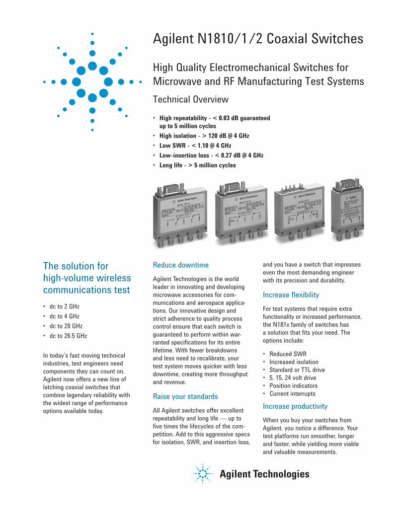
Agilent N1810/1 /2 Coaxial Switches
High Quality Electromechanical Switches for
Microwave and RF Manufacturing Test Systems
Technical Overview
The solution for high-volume wireless communications test
• dc to 2 GHz
• dc to 4 GHz
• dc to 20 GHz
• dc to 26.5 GHz
In today’s fast moving technical
industries, test engineers need
components they can count on.
Agilent now offers a new line of
latching coaxial switches that
combine legendary reliability with
the widest range of performance
options available today.
• High repeatability - < 0.03 dB guaranteed
up to 5 million cycles
• High isolation - > 120 dB @ 4 GHz
• Low SWR - < 1.10 @ 4 GHz
• Low-insertion loss - < 0.27 dB @ 4 GHz
• Long life - > 5 million cycles
Reduce downtime
Agilent Technologies is the world
leader in innovating and developing
microwave accessories for com-
munications and aerospace applica-
tions. Our innovative design and
strict adherence to quality process
control ensure that each switch is
guaranteed to perform within war-
ranted specifications for its entire
lifetime. With fewer breakdowns
and less need to recalibrate, your
test system moves quicker with less
downtime, creating more throughput
and revenue.
Raise your standards
All Agilent switches offer excellent
repeatability and long life — up to
five times the lifecycles of the com-
petition. Add to this aggressive specs
for isolation, SWR, and insertion loss,
and you have a switch that impresses
even the most demanding engineer
with its precision and durability.
Increase fl exibility
For test systems that require extra
functionality or increased performance,
the N181x family of switches has
a solution that fits your need. The
options include:
• Reduced SWR
• Increased isolation
• Standard or TTL drive
• 5, 15, 24 volt drive
• Position indicators
• Current interrupts
Increase productivity
When you buy your switches from
Agilent, you notice a difference. Your
test platforms run smoother, longer
and faster, while yielding more viable
and valuable measurements.
2
Description
N1810UL
Unterminated latching
The Agilent N1810UL is a single-pole
double-throw switch available in the
frequency range from dc to 26.5 GHz.
In precision measurements and
monitoring applications where inser-
tion loss repeatability is crucial, these
switches operate in excess of
5 million cycles with better than
.03 dB of insertion loss repeatability
at 25 °C.
N1810TL
Terminated latching
The Agilent N1810TL is a single-pole
double-throw switch available in the
frequency range from dc to 26.5 GHz.
The unused port is terminated 50 ohms,
making it ideal for applications where
port matching is required.
N1811TL
Terminated latching
The N1811TL is a terminated bypass
switch available in the frequency
range from dc to 26.5 GHz. The
switch’s internal load can terminate
the device under test when in the
bypass mode (up to 1 watt). Because
of its compact design, it is ideal for
drop-in, drop-out applications.
N1812UL
Unterminated latching
The N1812UL is a versatile, untermi-
nated 5-port switch available in the
frequency range from dc to 26.5 GHz.
In transfer switch applications, the
fifth port can be terminated externally
with a high-power termination. It
can also be utilized for signal path
reversal or as a calibration port.
Technology Operation
Agilent Technologies switches are
designed with a rectangular coaxial
structure similar to edge-line. This
transmission line structure provides
for movement of the edge-line
center conductor between two fixed,
continuous ground planes. The main
advantage of this innovation is that
the moving contacts can be easily
activated, yet maintain high-isolation
and low-insertion loss.
The RF contact configuration is
designed for controlled wiping action.
Since the outer conductor is not part
of the switching function, repeatability
and life are improved. The switching
action occurs typically within
15 milliseconds, after which perma-
nent magnets latch the contacts to
retain the new switch position.
All switches are “break before make”:
the switched ports are not connected
to each other. This prevents damage
to sensitive circuits and enhances
test simplicity.
Driving
There are two positions for the
N181x family of switches. Standard
switching is accomplished by apply-
ing the supply voltage to pin 5 (+V)
and grounding either pin 4 (A) or pin
3 (B) to actuate the mechanism to
the desired state. See page 5, pin-out
diagram.
Warning minimum switch spacing is
6.0 mm (0.25 inch).
When option 403 is added, the drive
current is automatically disconnected
after the switch is fully latched
(15 ms). Without option 403, the
switches MUST be actuated using a
pulse drive — the switches are not
designed to withstand continuous
current. In this case, the pulse dura-
tion must be at least 15 ms to ensure
that the switch will fully latch.
Option 401 drives the switch with
TTL/5V CMOS compatible logic,
which controls the DC power supply
to drive the switch.
Option 402 provides electronic
indication of switch state. The
circuitry consists of two independent
commons, which can be connected
to outputs corresponding to either
position A or B. Because the commons
are electrically isolated from each
other as well as the drive circuit, this
option allows two position signals to
be obtained.

3
Specifi cations
Specifications describe the instrument’s warranted performance. Supplemental
and typical characteristics are intended to provide information useful in applying
the instrument by giving typical, but not warranted performance parameters.
General
Input power (into load) 1 W, 7 V dc, 50 W pk, 10 µs max pulse duration, not to
exceed 1 W avg
Input power (into thru) 2 W, 7 V dc, 50 W pk, 10 µs max pulse duration, not to
exceed 2 W avg
Coil voltage 5, 15, 24 VDC
Connector SMA (f)
Standard performance specifi cations - N181x series
30Isolation (dB) = 90 - (–) F, where F is specified in GHz 26.5
dc 4 GHz 12.4 GHz 20 GHz 26.5 GHz
90 85 76 67 60
.45Insertion loss (dB) = 0.35 + (–) F, where F is specified in GHz 26.5
dc 4 GHz 12.4 GHz 20 GHz 26.5 GHz
0.35 0.42 0.56 0.69 0.80
SWR dc-4 GHz 4-12.4 GHz 12.4-20 GHz 20-26.5 GHz
1.15 1.25 1.30 1.60
Optional high-performance specifi cations - N181x series
35Isolation (dB) = 125 - (–) F, where F is specified in GHz 26.5
dc 4 GHz 12.4 GHz 20 GHz 26.5 GHz
Option 3011 125 120 109 99 90
.45Insertion loss (dB) = 0.20 + (–) F, where F is specified in GHz 26.5
dc 4 GHz 12.4 GHz 20 GHz 26.5 GHz
Option 302 0.2 0.27 0.41 0.53 0.65
SWR dc-4 GHz 4-12.4 GHz 12.4-20 GHz 20-26.5 GHz
Option 302 1.10 1.20 1.23 1.45
1. Option 301:
Environmental: Storage and cycling temperature: -55 C to +65 C
Environmental: Operating temperature: -25 C to +65 C

4
N1810UL
8.35.329
4.35.171
3.15.124
10.65.419
15.65.616
13.15.518
18.15.71420.65
.81328.151.1088.35
.329
4.35.171
4.39.173
11.89.468
8.35.329
16.89.665
21.89.862
19.39.763
29.391.157
4.32.170
2.36.093
1.79.071 11.39
.44830.201.189
11.00.433
12.70.500
6.35.250
5.89.232
33.781.330
11.00.433
8.16.321
48.671.916
44.741.761
53.412.103
16.89.665
6.35.250
16.89.665
6.35.250
Option 202Option 401
Option 201Option 401
Option 201
Option 202 Option 201
Typical
Typical
Option 202
3.05.120
2.40.094
2X
2X
Ø
Ø
5
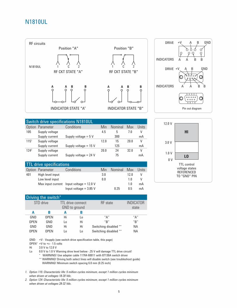
N1810UL
Switch drive specifications N1810ULOption Parameter Conditions Min Nominal Max Units105 Supply voltage 4.5 5 7.0 V
Supply current Supply voltage = 5 V 300 mA
1151 Supply voltage 12.0 15 20.0 V
Supply current Supply voltage = 15 V 125 mA
1242 Supply voltage 20.0 24 32.0 V
Supply current Supply voltage = 24 V 75 mA.
TTL drive specificationsOption Parameter Conditions Min Nominal Max Units401 High level input 3.0 12.0 V
Low level input 0.0 1.0 V
Max input current Input voltage = 12.0 V 1.0 mA
Input voltage = 3.85 V 0.25 0.5 mA
RF circuits
Position "A" Position "B"
N1810UL
RF CKT STATE "A" RF CKT STATE "B"
A A B B A A B B
1 C 2 1 C 2
INDICATOR STATE "A” INDICATOR STATE "B"
1. Option 115: Characteristic life: 5 million cycles minimum, except 1 million cycles minimum
when driven at voltages 18-20 Vdc.
2. Option 124: Characteristic life: 5 million cycles minimum, except 1 million cycles minimum
when driven at voltages 28-32 Vdc.
12.0 V
3.0 V
1.0 V
0 V
TTL controlvoltage statesREFERENCEDTO "GND" PIN
HI
LO
DRIVE
INDICATORS
DRIVE
INDICATORS
+V A B GND
A A B B
+V A B GND
A A B B
Pin out diagram
5 4 3 2 1
9 8 7 6
Driving the switch*STD drive TTL drive connect
GND to groundRF state INDICATOR
stateA B A B
GND OPEN Hi Lo “A” “A”
OPEN GND Lo Hi “B” “B”
GND GND Hi Hi Switching disabled ** NA
OPEN OPEN Lo Lo Switching disabled ** NA
GND: +V - Vsupply (see switch drive specifi cation table, this page)
OPEN* +V to +v - 1.5 volts
Hi 3.0 V to 12.0 V
Lo 0.0 V to 1.0 V Warning drive level below -.25 V will damage TTL drive circuit!
* WARNING! Use adapter cable 11764-60011 with 87130A switch driver
** WARNING! Driving both select lines will disable switch (see troubleshoot guide)
WARNING! Minimum switch spacing 6.0 mm (0.25 inch)

6
N1810TL
8.35.329
4.35.171
3.15.124
10.65.419
15.65.616
13.15.518
18.15.71420.65
.81328.151.1088.35
.329
4.35.171
4.39.173
11.89.468
14.39.567
16.89.665
21.89.862
19.39.763
29.391.157
4.32.170
2.36.093
1.79.071
11.39.448 52.20
2.055
11.00.433
12.70.500
6.35.250
16.89.665
55.782.196
11.00.433
8.16.321
48.671.916
44.741.761
53.412.103
16.89.665
6.35.250
16.89.665
6.35.250
Option 202Option 401
Option 201Option 401
Option 201
Option 202 Option 201
Typical
Typical
Option 202
3.05.120
2.40.094
4X 2XØ Ø
1 C 2
7
N1810TL
RF Circuits
Position "A" Position "B"
N1810TL
RF CKT STATE "A" RF CKT STATE "B"
A A B B A A B B
1 C 2 1 C 2
50 50 50 50
INDICATOR STATE "A" INDICATOR STATE "B"
12.0 V
3.0 V
1.0 V
0 V
TTL controlvoltage statesREFERENCEDTO "GND" PIN
HI
LO
DRIVE
INDICATORS
DRIVE
INDICATORS
+V A B GND
A A B B
+V A B GND
A A B B
Pin out diagram
5 4 3 2 1
9 8 7 6
Switch drive specifications N1810TL, N1811TL, N1812ULOption Parameter Conditions Min Nominal Max Units105 Supply voltage 4.5 5 7.0 V
Supply current Supply voltage = 5 V 600 mA
1151 Supply voltage 12.0 15 20.0 V
Supply current Supply voltage = 15 V 250 mA
1242 Supply voltage 20.0 24 32.0 V
Supply current Supply voltage = 24 V 150 mA.
TTL drive specificationsOption Parameter Conditions Min Nominal Max Units401 High level input 3.0 12.0 V
Low level input 0.0 1.0 V
Max input current Input voltage = 12.0 V 1.0 mA
Input voltage = 3.85 V 0.25 0.5 mA
1. Option 115: Characteristic life: 5 million cycles minimum, except 1 million cycles minimum
when driven at voltages 18-20 Vdc.
2. Option 124: Characteristic life: 5 million cycles minimum, except 1 million cycles minimum
when driven at voltages 28-32 Vdc.
Driving the switch*STD drive TTL drive connect
GND to groundRF state INDICATOR
stateA B A B
GND OPEN Hi Lo “A” “A”
OPEN GND Lo Hi “B” “B”
GND GND Hi Hi Switching disabled ** NA
OPEN OPEN Lo Lo Switching disabled ** NA
GND: +V - Vsupply (see switch drive specifi cation table, this page)
OPEN* +V to +v - 1.5 volts
Hi 3.0 V to 12.0 V
Lo 0.0 V to 1.0 V Warning drive level below -.25 V will damage TTL drive circuit!
* WARNING! Use adapter cable 11764-60011 with 87130A switch driver
** WARNING! Driving both select lines will disable switch (see troubleshoot guide)
WARNING! Minimum switch spacing 6.0 mm (0.25 inch)
8
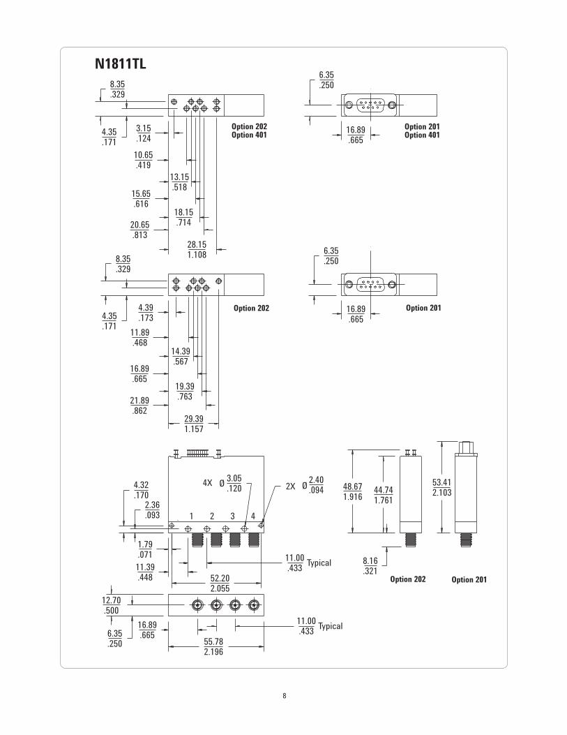
N1811TL
8.35.329
4.35.171
3.15.124
10.65.419
15.65.616
13.15.518
18.15.71420.65
.81328.151.1088.35
.329
4.35.171
4.39.173
11.89.468
14.39.567
16.89.665
21.89.862
19.39.763
29.391.157
4.32.170
2.36.093
1.79.071
11.39.448 52.20
2.055
11.00.433
12.70.500
6.35.250
16.89.665
55.782.196
11.00.433
8.16.321
48.671.916
44.741.761
53.412.103
16.89.665
6.35.250
16.89.665
6.35.250
Option 202Option 401
Option 201Option 401
Option 201
Option 202 Option 201
Typical
Typical
Option 202
3.05.120
2.40.094
4X 2XØ Ø
1 2 3 4

9
N1811TL
RF Circuits
Position "A" Position "B"
N1811TL
RF CKT STATE "A" RF CKT STATE "B"
A A B B A A B B
1 2 3 4 1 2 3 4
50 50
INDICATOR STATE "A” INDICATOR STATE "B"
12.0 V
3.0 V
1.0 V
0 V
TTL controlvoltage statesREFERENCEDTO "GND" PIN
HI
LO
DRIVE
INDICATORS
DRIVE
INDICATORS
+V A B GND
A A B B
+V A B GND
A A B B
Pin out diagram
5 4 3 2 1
9 8 7 6
Switch drive specifications N1810TL, N1811TL, N1812ULOption Parameter Conditions Min Nominal Max Units105 Supply voltage 4.5 5 7.0 V
Supply current Supply voltage = 5 V 600 mA
1151 Supply voltage 12.0 15 20.0 V
Supply current Supply voltage = 15 V 250 mA
1242 Supply voltage 20.0 24 32.0 V
Supply current Supply voltage = 24 V 150 mA.
TTL Drive specificationsOption Parameter Conditions Min Nominal Max Units401 High level input 3.0 12.0 V
Low level input 0.0 1.0 V
Max input current Input voltage = 12.0 V 1.0 mA
Input voltage = 3.85 V 0.25 0.5 mA
1. Option 115: Characteristic life: 5 million cycles minimum, except 1 million cycles minimum
when driven at voltages 18-20 Vdc.
2. Option 124: Characteristic life: 5 million cycles minimum, except 1 million cycles minimum
when driven at voltages 28-32 Vdc.
Driving the switch*STD drive TTL drive connect
GND to groundRF state INDICATOR
stateA B A B
GND OPEN Hi Lo “A” “A”
OPEN GND Lo Hi “B” “B”
GND GND Hi Hi Switching disabled ** NA
OPEN OPEN Lo Lo Switching disabled ** NA
GND: +V - Vsupply (see switch drive specifi cation table, this page)
OPEN* +V to +v - 1.5 volts
Hi 3.0 V to 12.0 V
Lo 0.0 V to 1.0 V Warning drive level below -.25 V will damage TTL drive circuit!
* WARNING! Use adapter cable 11764-60011 with 87130A switch driver
** WARNING! Driving both select lines will disable switch (see troubleshoot guide)
WARNING! Minimum switch spacing 6.0 mm (0.25 inch)
10
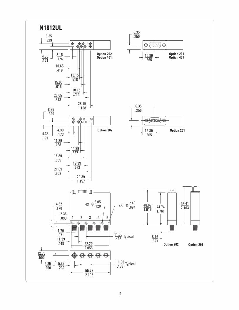
N1812UL
8.35.329
4.35.171
3.15.124
10.65.419
15.65.616
13.15.518
18.15.71420.65
.81328.151.1088.35
.329
4.35.171
4.39.173
11.89.468
14.39.567
16.89.665
21.89.862
19.39.763
29.391.157
4.32.170
2.36.093
1.79.07111.39.448 52.20
2.055
11.00.433
12.70.500
6.35.250
5.89.232
55.782.196
11.00.433
8.16.321
48.671.916
44.741.761
53.412.103
16.89.665
6.35.250
16.89.665
6.35.250
Option 202Option 401
Option 201Option 401
Option 201
Option 202 Option 201
Typical
Typical
Option 202
3.05.120
2.40.094
4X 2XØ Ø
1 2 3 4 5

11
N1812UL
RF Circuits
Position "A" Position "B"
N1812UL
RF CKT STATE "A" RF CKT STATE "B"
A A B B A A B B
1 2 3 4 5 1 2 3 4 5
INDICATOR STATE "A" INDICATOR STATE "B"
12.0 V
3.0 V
1.0 V
0 V
TTL controlvoltage statesREFERENCEDTO "GND" PIN
HI
LO
DRIVE
INDICATORS
DRIVE
INDICATORS
+V A B GND
A A B B
+V A B GND
A A B B
Pin out diagram
5 4 3 2 1
9 8 7 6
Switch drive specifications N1810TL, N1811TL, N1812ULOption Parameter Conditions Min Nominal Max Units105 Supply voltage 4.5 5 7.0 V
Supply current Supply voltage = 5 V 600 mA
1151 Supply voltage 12.0 15 20.0 V
Supply current Supply voltage = 15 V 250 mA
1242 Supply voltage 20.0 24 32.0 V
Supply current Supply voltage = 24 V 150 mA.
TTL drive specificationsOption Parameter Conditions Min Nominal Max Units401 High level input 3.0 12.0 V
Low level input 0.0 1.0 V
Max input current Input voltage = 12.0 V 1.0 mA
Input voltage = 3.85 V 0.25 0.5 mA
1. Option 115: Characteristic life: 5 million cycles minimum, except 1 million cycles minimum
when driven at voltages 18-20 Vdc.
2. Option 124: Characteristic life: 5 million cycles minimum, except 1 million cycles minimum
when driven at voltages 28-32 Vdc.
Driving the switch*STD drive TTL drive connect
GND to groundRF state INDICATOR
stateA B A B
GND OPEN Hi Lo “A” “A”
OPEN GND Lo Hi “B” “B”
GND GND Hi Hi Switching disabled ** NA
OPEN OPEN Lo Lo Switching disabled ** NA
GND: +V - Vsupply (see switch drive specifi cation table, this page)
OPEN* +V to +v - 1.5 volts
Hi 3.0 V to 12.0 V
Lo 0.0 V to 1.0 V Warning drive level below -.25 V will damage TTL drive circuit!
* WARNING! Use adapter cable 11764-60011 with 87130A switch driver
** WARNING! Driving both select lines will disable switch (see troubleshoot guide)
WARNING! Minimum switch spacing 6.0 mm (0.25 inch)
12
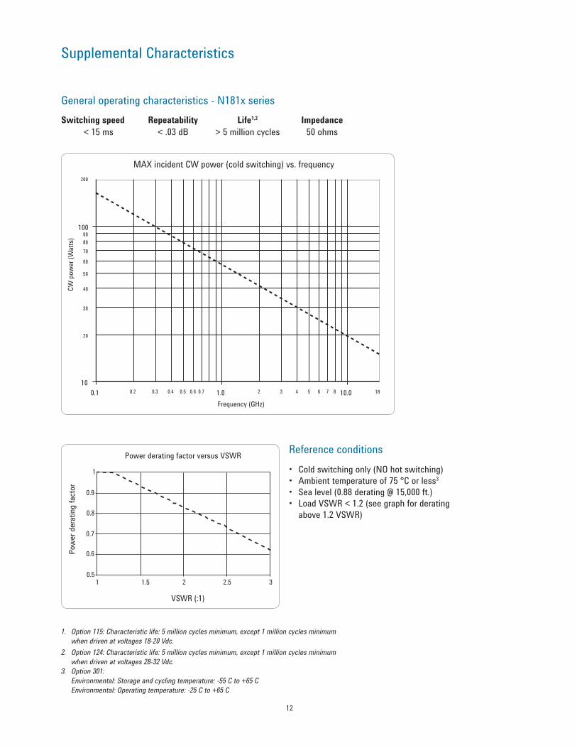
Supplemental Characteristics
General operating characteristics - N181x series
Switching speed Repeatability Life1,2 Impedance
< 15 ms < .03 dB > 5 million cycles 50 ohms
1. Option 115: Characteristic life: 5 million cycles minimum, except 1 million cycles minimum
when driven at voltages 18-20 Vdc.
2. Option 124: Characteristic life: 5 million cycles minimum, except 1 million cycles minimum
when driven at voltages 28-32 Vdc.
3. Option 301:
Environmental: Storage and cycling temperature: -55 C to +65 C
Environmental: Operating temperature: -25 C to +65 C
Reference conditions
• Cold switching only (NO hot switching)
• Ambient temperature of 75 °C or less3
• Sea level (0.88 derating @ 15,000 ft.)
• Load VSWR < 1.2 (see graph for derating
above 1.2 VSWR)
0.1 1.0 10.00.2 0.3 0.4 0.5 0.6 0.7 2 3 4 5 6 7 8
Frequency (GHz)
10
100
20
30
40
50
60
70
80
90
CW
pow
er (
Wat
ts)
18
200
MAX incident CW power (cold switching) vs. frequency
Power derating factor versus VSWR
Pow
er d
erat
ing
fact
or
VSWR (:1)
1 1.5 2 2.5 3
1
0.9
0.8
0.7
0.6
0.5
13
Environmental
The switch is designed to fully comply with Agilent Technologies’ product oper-
ating environment specifications. The following summarizes the environmental
specifications for these products (Class B1).
Temperature1
Operating: -25 to +75 °C
Storage: -55 to +85 °C
Cycling: -55 to +85 °C, 10 cycles per MIL-STD 202F, 170D, Condition A
(modified)
Vibration
Operating: 7 g, 5-2000 Hz @ 0.25 in. p-p
Survival: 20 g, 20-2000 Hz @ 0.06 in. p-p, 4 min/cycle, 4 cycles/axis
Random: 2.41 g (rms.) 10 min/axis
Shock: Half sine: 500 g @ 0.5 ms, 3 drops/direction, 18 total
Operating: 50 g @ 6 ms, 6 directions
Humidity
Operating: 15 to 95 % relative humidity
Storage: 65 °C, 95 % RH, 10 days, MIL-STD 202F, Method 106E
Altitude
Operating: 15,000 feet / 4.6 km
Storage: 50,000 feet / 15.3 km, MIL-STD 202F, Method 105C, Condition B
1. Option 301:
Environmental: Storage and cycling temperature: -55 C to +65 C
Environmental: Operating temperature: -25 C to +65 C
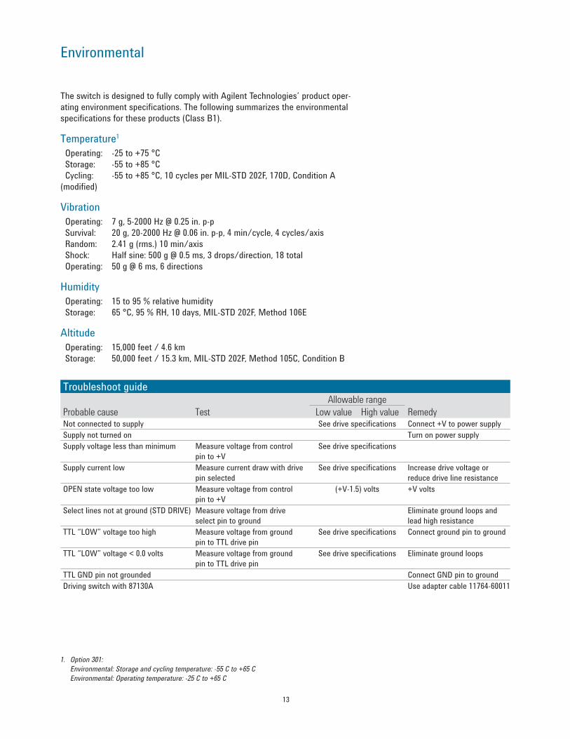
Troubleshoot guide Allowable range
Probable cause Test Low value High value RemedyNot connected to supply See drive specifi cations Connect +V to power supply
Supply not turned on Turn on power supply
Supply voltage less than minimum Measure voltage from control
pin to +V
See drive specifi cations
Supply current low Measure current draw with drive
pin selected
See drive specifi cations Increase drive voltage or
reduce drive line resistance
OPEN state voltage too low Measure voltage from control
pin to +V
(+V-1.5) volts +V volts
Select lines not at ground (STD DRIVE) Measure voltage from drive
select pin to ground
Eliminate ground loops and
lead high resistance
TTL “LOW” voltage too high Measure voltage from ground
pin to TTL drive pin
See drive specifi cations Connect ground pin to ground
TTL “LOW” voltage < 0.0 volts Measure voltage from ground
pin to TTL drive pin
See drive specifi cations Eliminate ground loops
TTL GND pin not grounded Connect GND pin to ground
Driving switch with 87130A Use adapter cable 11764-60011
14
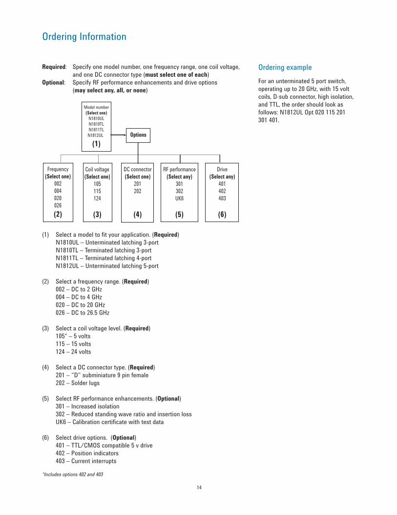
Ordering Information
(1) Select a model to fit your application. (Required)
N1810UL – Unterminated latching 3-port
N1810TL – Terminated latching 3-port
N1811TL – Terminated latching 4-port
N1812UL – Unterminated latching 5-port
(2) Select a frequency range. (Required)
002 – DC to 2 GHz
004 – DC to 4 GHz
020 – DC to 20 GHz
026 – DC to 26.5 GHz
(3) Select a coil voltage level. (Required)
105* – 5 volts
115 – 15 volts
124 – 24 volts
(4) Select a DC connector type. (Required)
201 – “D” subminiature 9 pin female
202 – Solder lugs
(5) Select RF performance enhancements. (Optional)
301 – Increased isolation
302 – Reduced standing wave ratio and insertion loss
UK6 – Calibration certificate with test data
(6) Select drive options. (Optional)
401 – TTL/CMOS compatible 5 v drive
402 – Position indicators
403 – Current interrupts
Model number
(Select one)
N1810UL
N1810TL
N1811TL
N1812UL
(1)
Options
Frequency
(Select one)
002
004
020
026
(2)
Coil voltage
(Select one)
105
115
124
(3)
DC connector
(Select one)
201
202
(4)
RF performance
(Select any)
301
302
UK6
(5)
Drive
(Select any)
401
402
403
(6)
Ordering example
For an unterminated 5 port switch,
operating up to 20 GHz, with 15 volt
coils, D-sub connector, high isolation,
and TTL, the order should look as
follows: N1812UL Opt 020 115 201
301 401.
*Includes options 402 and 403
Required: Specify one model number, one frequency range, one coil voltage,
and one DC connector type (must select one of each)
Optional: Specify RF performance enhancements and drive options
(may select any, all, or none)
Remove all doubt
Our repair and calibration services
will get your equipment back to you,
performing like new, when prom-
ised. You will get full value out of
your Agilent equipment through-
out its lifetime. Your equipment
will be serviced by Agilent-trained
technicians using the latest factory
calibration procedures, automated
repair diagnostics and genuine parts.
You will always have the utmost
confi dence in your measurements.
For information regarding self
maintenance of this product, please
contact your Agilent offi ce.
Agilent offers a wide range of ad-
ditional expert test and measure-
ment services for your equipment,
including initial start-up assistance,
onsite education and training, as
well as design, system integration,
and project management.
For more information on repair and
calibration services, go to:
www.agilent.com/find/removealldoubt
For more information on Agilent Technologies’ products, applications or services, please contact your local Agilent
office. The complete list is available at:
www.agilent.com/find/contactus
AmericasCanada (877) 894-4414 Latin America 305 269 7500United States (800) 829-4444
Asia PacificAustralia 1 800 629485China 800 810 0189Hong Kong 800 938 693India 1 800 112 929Japan 0120 (421) 345Korea 080 769 0800Malaysia 1 800 888 848Singapore 1 800 375 8100Taiwan 0800 047 866Thailand 1 800 226 008
Europe & Middle EastAustria 01 36027 71571Belgium 32 (0) 2 404 93 40 Denmark 45 70 13 15 15Finland 358 (0) 10 855 2100France 0825 010 700* *0.125 €/minute
Germany 07031 464 6333Ireland 1890 924 204Israel 972-3-9288-504/544Italy 39 02 92 60 8484Netherlands 31 (0) 20 547 2111Spain 34 (91) 631 3300Sweden 0200-88 22 55Switzerland 0800 80 53 53United Kingdom 44 (0) 118 9276201Other European Countries: www.agilent.com/find/contactusRevised: October 1, 2008
© Agilent Technologies, Inc. 2001, 2002, 2007, 2009Printed in USA, March 12, 20095968-9653E
Product specifi cations and descriptions in this document subject to change without notice.
www.agilent.comwww.agilent.com/find/switcheswww.agilent.com/find/mta
Agilent Email Updates
www.agilent.com/find/emailupdates
Get the latest information on the
products and applications you select.
Agilent Direct
www.agilent.com/find/agilentdirect
Quickly choose and use your test
equipment solutions with confidence.
AgilentOpen
www.agilent.com/find/open
Agilent Open simplifies the process
of connecting and programming
test systems to help engineers
design, validate and manufacture
electronic products. Agilent offers
open connectivity for a broad range
of system-ready instruments, open
industry software, PC-standard
I/O and global support, which are
combined to more easily integrate
test system development.
www.lxistandard.org
LXI is the LAN-based successor to
GPIB, providing faster, more efficient
connectivity. Agilent is a founding
member of the LXI consortium.