Embed Size (px)
Citation preview

Automated jitter tolerance compliance and characterization
Calibrated jitter composition
Integrated into one box
Compliant to latest serial bus standards
Smartest Characterization andCompliance
Key Capabilities:
• Integrated and calibrated jitter sources: PJ, SJ, RJ, BUJ, ISI and sinusoidal interference
• Jitter tolerance testing: PCI Express®, SATA, Fibre Channel, FB-DIMM, CEI, 10 GbE, XFP/XFI
• Quick eye masks and BER contours• Bit recovery mode for analyzing undeterministic
patterns• SSC generation• CDR with tunable loop bandwidth for compliant
measurements for all data rates• Pattern sequencer and capture to simplify the
handling of complex data patterns • Subrate clock outputs• Pattern generator options• All options upgradable
Version 3.1New: Fastest Jitter Tolerance Results (SW 4.5)New: Pattern Generator (options G07 and G13)Includes specifications for tunable CDR(options CTR, UTR)
Agilent J-BERT N4903A High-Performance Serial BERTwith Complete Jitter ToleranceTesting
7 Gb/s and 12.5 Gb/s
Data Sheet
J-BERT N4903A High-Performance Serial BERT Data Sheet
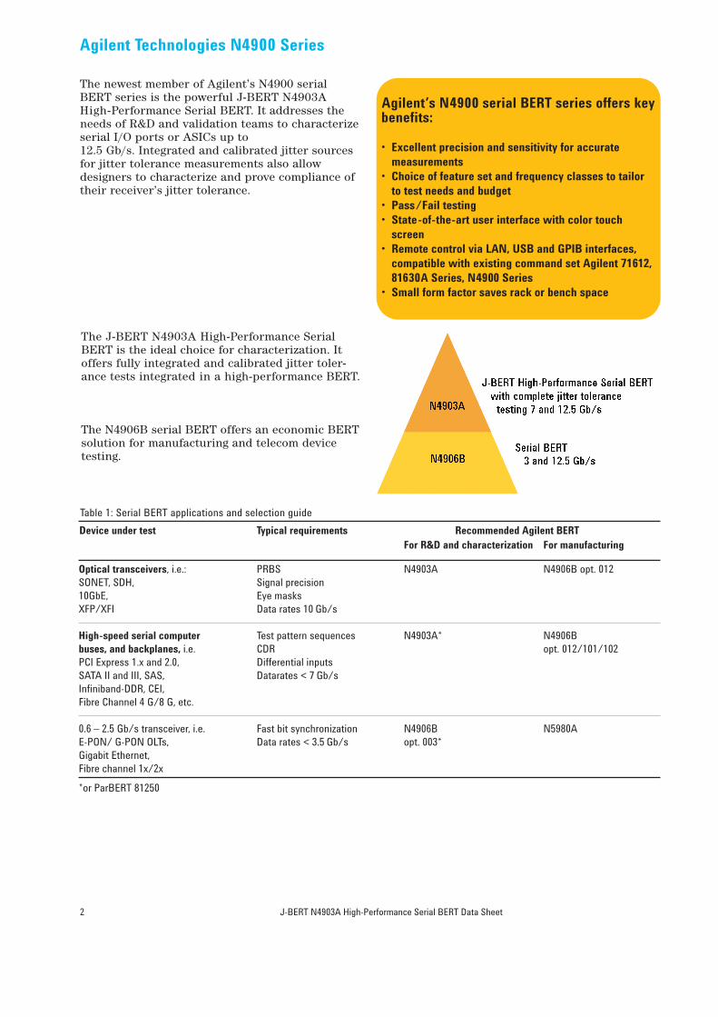
Table 1: Serial BERT applications and selection guide
Device under test Typical requirements Recommended Agilent BERT For R&D and characterization For manufacturing
Optical transceivers, i.e.: PRBS N4903A N4906B opt. 012SONET, SDH, Signal precision10GbE, Eye masksXFP/XFI Data rates 10 Gb/s
High-speed serial computer Test pattern sequences N4903A* N4906Bbuses, and backplanes, i.e. CDR opt. 012/101/102PCI Express 1.x and 2.0, Differential inputsSATA II and III, SAS, Datarates < 7 Gb/sInfiniband-DDR, CEI,Fibre Channel 4 G/8 G, etc.
0.6 – 2.5 Gb/s transceiver, i.e. Fast bit synchronization N4906B N5980AE-PON/ G-PON OLTs, Data rates < 3.5 Gb/s opt. 003* Gigabit Ethernet,Fibre channel 1x/2x
*or ParBERT 81250
The newest member of Agilent’s N4900 serialBERT series is the powerful J-BERT N4903AHigh-Performance Serial BERT. It addresses theneeds of R&D and validation teams to characterizeserial I/O ports or ASICs up to 12.5 Gb/s. Integrated and calibrated jitter sourcesfor jitter tolerance measurements also allowdesigners to characterize and prove compliance oftheir receiver’s jitter tolerance.
The J-BERT N4903A High-Performance SerialBERT is the ideal choice for characterization. Itoffers fully integrated and calibrated jitter toler-ance tests integrated in a high-performance BERT.
The N4906B serial BERT offers an economic BERTsolution for manufacturing and telecom devicetesting.
2
Agilent’s N4900 serial BERT series offers keybenefits:
• Excellent precision and sensitivity for accurate measurements
• Choice of feature set and frequency classes to tailor to test needs and budget
• Pass/Fail testing• State-of-the-art user interface with color touch
screen• Remote control via LAN, USB and GPIB interfaces,
compatible with existing command set Agilent 71612, 81630A Series, N4900 Series
• Small form factor saves rack or bench space
Agilent Technologies N4900 Series

Available J-BERT configurations
BERT pattern generator and error detector,including built-in CDRBERT 150 Mb/s to 12.5 Gb/s N4903A-C13BERT 150 Mb/s to 7 Gb/s N4903A-C07
Pattern generator (PG) options*only in combination with -J10PG 150 Mb/s to 12.5 Gb/s* N4903A-G13PG 150 Mb/s to 7 Gb/s* N4903A-G07SSC clocking* N4903A-J11
Jitter tolerance optionsRJ, PJ, SJ, BUJ injection N4903A-J10ISI and sinusoidal N4903A-J20interference injectionJitter tol. compliance suite N4903A-J12
Error detector optionsBit recovery mode N4903A-A01Compliant CDR N4903A-CTRwith tunable loop bandwidth
UpgradesAll options upgradable (see page 17)
The J-BERT N4903A High-Performance SerialBERT provides the only complete jitter tolerancetest. It is the ideal choice for R&D and validationteams characterizing and stressing chips andtransceiver modules that have serial I/O ports upto 7 Gb/s or 12.5 Gb/s. It can characterize areceiver’s jitter tolerance and prove its complianceto today’s most popular standards, such as PCIExpress, SATA, Fibre Channel, Fully BufferedDIMM, CEI, 10 GbE/ XAUI and XFP/XFI.
Accurate characterization is achieved with cleansignals from the pattern generator, which featuresexceptionally low jitter and extremely fast transi-tion times. Test set-up time is reduced signifi-cantly, because the J-BERT N4903A matches mostrecent serial bus standards optimally: • Undeterministic patterns can now be analyzed
with the bit recovery mode. • A pattern sequencer helps to set up training
sequences quickly, to get complex devices into loop-back test mode.
• Reference clocks can be provided by the sub-rate clock outputs, which can generate any ratioof clock to data rate.
• All I/Os are differential and a built-in CDRallows testing of clockless interfaces.
The J-BERT N4903A is a future proof serialBERT platform, which is configurable for today’stest and budget requirements but also allowsupgrades to all options and full speed.
Measurements
BER and measurement suite• BERT scan• Output timing jitter• Spectral jitter decomposition• Eye contour• Quick eye diagram and BER contour• Fast eye mask• Output level and Q factor• Error location capture• Fast total jitter• Pattern capture
Jitter tolerance tests• Manual jitter composition (option J10)• Automated jitter tolerance • Characterization (option J10)• Automated jitter tolerance compliance
(option J12)
Applications
• PCI Express• SATA• Fibre channel• Fully buffered DIMM• CEI• 10 GbE/XAUI• XFP/XFI
J-BERT N4903A High-Performance Serial BERT Data Sheet 3
J-BERT key characteristics:
• 150 Mb/s to 7 Gb/s or 12.5 Gb/s – enough margin forcharacterizing today’s most popular serial interfaces
• Calibrated and integrated jitter injection (opt. J10).All in one box: RJ, PJ, BUJ, ISI, sinusoidal interfer-ence to stress the receiver with > 50 % eye closure
• Automated and compliant jitter tolerance tests coverspopular serial bus standards: PCI Express, SATA, FibreChannel, SATA, FB-DIMM, CEI 6G/11G, 10 GbE/XAUI,XFP/XFI
• Delay control input for generator to apply any externaljitter source
• Bit recovery mode to test unknown data traffic• Pattern sequencer to generate complex training
sequences • SSC clocking for computer buses • Subrate clocks to generate reference clocks easily• Differential I/O for DATA and CLOCK and most supple-
mentary signals for testing serial interfaces• Integrated CDR (clock data recovery) to test clock-
less devices from 1 to 12.5 Gb/s• Compliant and tunable loop bandwidth (opt. CTR)• Highest performance BERT for accurate
measurements• Remote operation of GUI via web server• All options retrofitable
J-BERT N4903A High-Performance Serial BERT
J-BERT N4903A High-Performance Serial BERT Data Sheet4
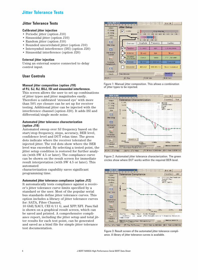
Figure 1: Manual jitter composition. This allows a combinationof jitter types to be injected.
Jitter Tolerance Tests
Calibrated jitter injection• Periodic jitter (option J10)• Sinusoidal jitter (option J10)• Random jitter (option J10)• Bounded uncorrelated jitter (option J10)• Intersymbol interference (ISI) (option J20)• Sinusoidal interference (option J20)
External jitter injectionUsing an external source connected to delay control input.
User Controls
Manual jitter composition (option J10)of PJ, SJ, RJ, BUJ, ISI and sinusoidal interference.This screen allows the user to set up combinationsof jitter types and jitter magnitudes easily.Therefore a calibrated ‘stressed eye’ with morethan 50% eye closure can be set up for receivertesting. Additional jitter can be injected with theinterference channel (option J20). It adds ISI anddifferential/single mode noise.
Automated jitter tolerance characterization (option J10)Automated sweep over SJ frequency based on thestart/stop frequency, steps, accuracy, BER level,confidence level and DUT relax time. The greendots indicate where the receiver tolerated theinjected jitter. The red dots show where the BERlevel was exceeded. By selecting a tested point, thejitter setup condition is restored for further analy-sis (with SW 4.5 or later). The compliance curvecan be shown on the result screen for immediateresult interpretation (with SW 4.5 or later). Thisautomated characterization capability saves significant programming time.
Automated jitter tolerance compliance (option J12)It automatically tests compliance against a receiv-er’s jitter tolerance curve limits specified by astandard or the user. Most of the popular serialbus standards define jitter tolerance curves. Thisoption includes a library of jitter tolerance curvesfor: SATA, Fibre Channel, 10 GbE/XAUI, CEI 6/11 G, and XFP/XFI. Pass/failis shown on a graphical result screen, which canbe saved and printed. A comprehensive compli-ance report, including the jitter setup and total jit-ter results for each test point, can be generatedand saved as a html file for simple jitter tolerancetest documentation.
Figure 2: Automated jitter tolerance characterization. The greencircles show where DUT works within the required BER-level.
Figure 3: Result screen of the automated jitter tolerance compli-ance. A library of jitter tolerance curves is available.
Jitter Tolerance Tests

J-BERT N4903A High-Performance Serial BERT Data Sheet
Figure 5: Spectral jitter decomposition for debugging jitter sources in a design.
Figure 6: Eye contour with colors indicating BER level.
Figure 7: BERT scan including RJ/DJ separation, total jitter.
User Interface and Measurement Suite
Quick eye diagram and maskingThe quick eye diagram allows a one-shot check fora valid signal. Due to the higher sampling depth ofa BERT, the eye contour lines visualize the meas-ured eye at a deeper BER level for more accurateresults. Extrapolated eye contour lines display theeye opening for even lower BER levels, such as 10-15, reducing the measurement time significantly.The display shows numerical results for 1-/0-level, eye amplitude and width, total jitter andmore. Eye masks can be loaded from a library.Violations of the captured eye mask are displayed.The result screen can be printed and saved fordocumenting test results (see figure 4).
Spectral jitter decompositionIt measures the spectral decomposition of jittercomponents. When debugging designs, the jitterdecomposition simplifies identifying deterministicjitter sources (see figure 5).
Eye contourThe eye opening is a key characteristic of a device.The BER is displayed as a function of samplingdelay and sampling threshold. Different views areavailable: eye contour (see figure 6), pseudo colorsand equal BER plots.
BERT scan including RJ/DJ separationThis measurement shows the BER versus the sam-pling point delay, which is displayed as a “bathtub”curve or as a histogram. The measurement resultsare displayed in a table with setup and hold timeover phase margin, total jitter in rms or peak- to -peak, and random and deterministic jitter. Themeasurement method is equivalent to IEEE802.3ae (see figure 7).
Figure 4: Quick eye diagram with BER contour and masking.
5
User Interface
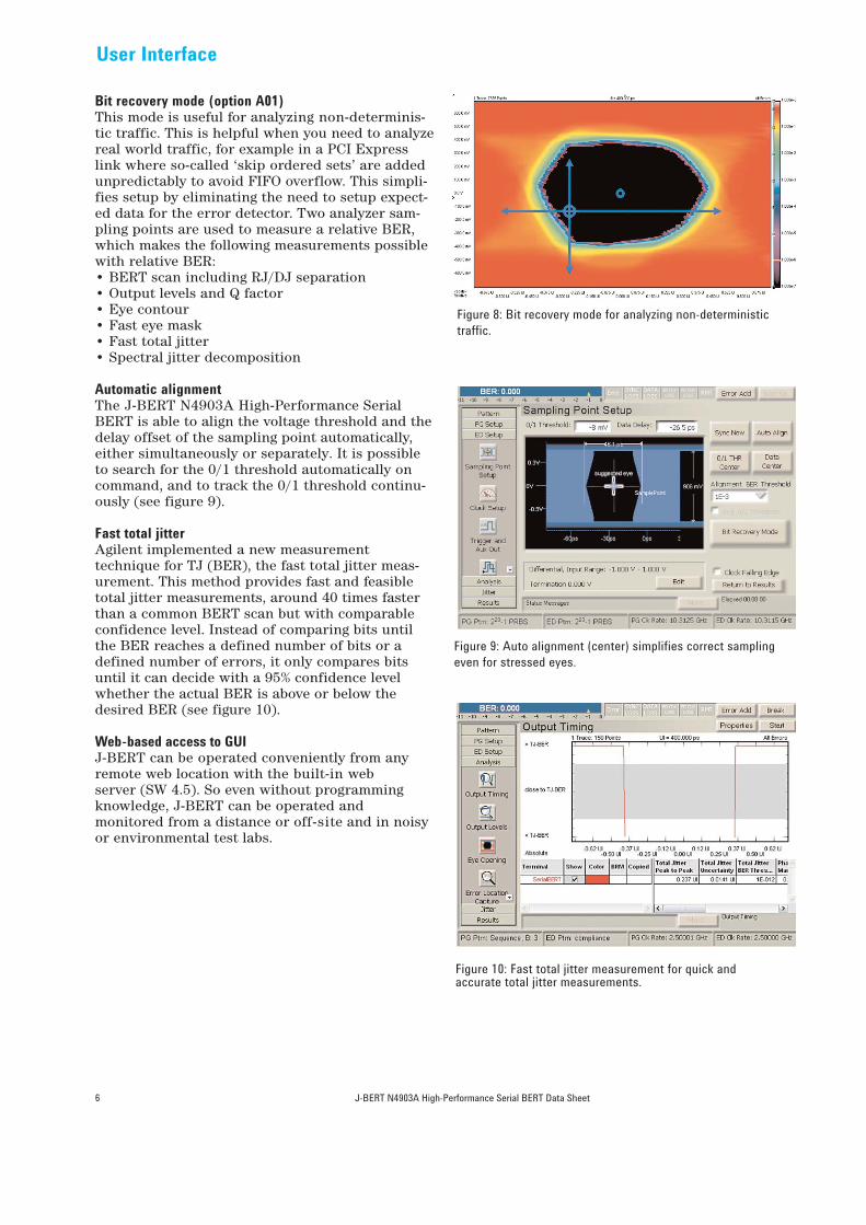
Figure 8: Bit recovery mode for analyzing non-deterministic traffic.
6 J-BERT N4903A High-Performance Serial BERT Data Sheet
Bit recovery mode (option A01)This mode is useful for analyzing non-determinis-tic traffic. This is helpful when you need to analyzereal world traffic, for example in a PCI Expresslink where so-called ‘skip ordered sets’ are addedunpredictably to avoid FIFO overflow. This simpli-fies setup by eliminating the need to setup expect-ed data for the error detector. Two analyzer sam-pling points are used to measure a relative BER,which makes the following measurements possiblewith relative BER:• BERT scan including RJ/DJ separation• Output levels and Q factor• Eye contour• Fast eye mask• Fast total jitter• Spectral jitter decomposition
Automatic alignmentThe J-BERT N4903A High-Performance SerialBERT is able to align the voltage threshold and thedelay offset of the sampling point automatically,either simultaneously or separately. It is possibleto search for the 0/1 threshold automatically oncommand, and to track the 0/1 threshold continu-ously (see figure 9).
Fast total jitterAgilent implemented a new measurement technique for TJ (BER), the fast total jitter meas-urement. This method provides fast and feasibletotal jitter measurements, around 40 times fasterthan a common BERT scan but with comparableconfidence level. Instead of comparing bits untilthe BER reaches a defined number of bits or adefined number of errors, it only compares bitsuntil it can decide with a 95% confidence levelwhether the actual BER is above or below thedesired BER (see figure 10).
Web-based access to GUIJ-BERT can be operated conveniently from anyremote web location with the built-in web server (SW 4.5). So even without programmingknowledge, J-BERT can be operated and monitored from a distance or off-site and in noisyor environmental test labs.
Figure 9: Auto alignment (center) simplifies correct samplingeven for stressed eyes.
Figure 10: Fast total jitter measurement for quick andaccurate total jitter measurements.
User Interface

Table 2: Output characteristics for J-BERT N4903A generator. Alltiming parameters are measured at ECL levels.Range of operation 150 Mb/s to 12.5 Gb/s (opt. C13)
Can be programmed up to 13.5 Gb/s150 Mb/s to 7 Gb/s (opt. C07)< 620 MHz only with externalclock
Frequency accuracy ± 15 ppm typicalFormat NRZ, normal or invertedAmplitude/resolution 0.10 V to 1.8 V, 5 mV steps
Addresses LVDS, CML, PECL,ECL (terminated to 1.3 V/0 V/-2 V), low voltage CMOS
Output voltage window -- 2.0 V to +3.0 VPredefined levels ECL, PECL (3.3 V), LVDS, CMLTransition times (20% to 80%) < 20 ps(10% to 90%) 1) < 25 psJitter 9 ps pp typical with disabled jitter
sources and internal clockClock/data delay range ± 0.75 ns in 100 fs stepsExternal termination -- 2 V to +3 Vvoltage 2)
Crossing point Adjustable 20% to 80% typical to emulate duty cycle distortions
Single error inject Adds single errors on demandFixed error inject Fixed error ratios of 1 error in
10n bits, n = 3, 4, 5, 6, 7, 8, 9Interface 3) Differential or single-ended,
DC coupled, 50WConnector 2.4 mm female
1) At 10 Gb/s and 7 Gb/s2) For positive termination voltage or termination to GND, external
termination voltage must be less than 3 V below VOH. Fornegative termination voltage, external termination voltage must be less than 2 V below VOH. External termination voltage must be less than 3 V above VOL.
3) Unused outputs must be terminated with 50W to GND.
J-BERT N4903A High-Performance Serial BERT Data Sheet
Figure 12: Clean output signal. 10 Gb/s, LVDS levels.
Figure 13: Pattern generator setup screen with graphical display of signal levels.
Figure 11: Generator connectors on front panel
Data output (DATA OUT)
Pattern Generator Specifications
7
Pattern generator key characteristics:
• Available as 7 and 12.5 Gb/s pattern generator with-out error detector (opt. G07 and G13)
• Differential outputs for data, clocks and trigger• Variable output voltages covering LVDS, ECL, CML• Transitions times < 20 ps• Clean pulses with jitter < 9 ps pp• High precision delay control input to inject jitter from
an external source• Calibrated and integrated jitter injection
(options J10, J20, both retrofitable)• Subrate clocks for generating any reference clock• Pattern sequencing and 32 Mbit pattern• SSC clocks for computer buses (option J11)
Specifications-Pattern Generator

Table 7: Specifications for subrate clock output
Divider factors n = 2,3…128Levels High: + 0.5 V
Low: --0.5 V typicalTransition times 35 ps typicalInterface DC coupled, 50 W, differential
or single-endedConnector SMA female
Table 8: Specifications for the 10 MHz reference outputAmplitude 1V into 50 W typicalInterface AC coupled,
50 W output impedanceConnector BNC, rear panel
8 J-BERT N4903A High-Performance Serial BERT Data Sheet
Clock output (CLK OUT)
Table 3: Clock output characteristics. All timing parametersare measured at ECL levels.Frequency range 150 MHz to 12.5 GHz (opt. C13)
Can be programmed up to 13.5 GHz150 MHz to 7 GHz (opt. C07)<620 MHz only with external clock
Amplitude/resolution 0.1 V pp to 1.8 V pp, 5 mV stepsOutput voltage window --2.00 to +2.8 VTransition times (20% to 80%) < 20 ps(10% to 90%)1) < 25 psExternal termination --2 V to +3 Vvoltage 2)
Jitter 1 ps rms typical with disabled jitter sources and internal clock
SSB phase noise < --75 dBc with internalclock source, 10 GHz @ 10kHz offset, 1 Hz bandwidth
Interface 3) Differential or single-ended,DC coupled, 50 W output impedance
Connector 2.4 mm female
1) At 10 Gb/s and 7 Gb/s2) For positive termination voltage or termination to GND, external
termination voltage must be less than 3 V below VOH. For negative termination voltage, external termination voltage must be less than 2 V below VOH. External termination voltage must be less than 3 V above VOL.
3) Unused outputs must be terminated with 50 W to GND.
Table 4: Specifications for clock input and 10 MHz referenceinputAmplitude 200 mV to 2 VInterface AC coupled, 50 W nominalConnectors
- Clock input: SMA female, front panel- 10 MHz reference input: BNC, rear panel
Clock Input (CLK IN)There are two modes when using the clock input con-nector.External Clock mode: all output signals of the gener-ator follow the external clock and its modulation.Nevertheless, the modulation of the external clockmust be within the same range given for SSC and SJ(see tables 11 and 21) or the 500 ps delay line. Whenusing External Clock mode the internal SSC and SJsources and the 500 ps delay line for PJ injection aredisabled. Modulation using the 200 ps delay line is still available (see figure 24).External PLL mode: it is used to lock the generatorto an external clock at the same data rate. The pro-vided clock must not be modulated in external PLLmode. All internal jitter sources are available.
Delay control input (DELAY CTRL IN)The external signal applied to delay control input, variesthe delay between data output and clock output. This canbe used to generate jittered signals to stress the deviceunder test in addition to the calibrated jitter injectionfrom N4903A.
Error add input (ERROR ADD)The external error add input adds a single error to thedata output for each rising edge at the input.
Subrate clock output (SUB CLK OUT)The subrate clock output is used to generate reference clocks, which are subrates of the data rate, forexample, a 100 MHz clock for 2.5 or 5 Gb/s PCI Express data rate.
10 MHz reference input (10 MHz REF IN)It is used to lock the generator to an external 10 MHzreference clock. The data rate can be selected withinthe same range as if the internal clock would be used.The provided reference clock must not be modulated.All internal jitter sources are available.
Specifications-Pattern Generator
Table 5: Specifications for delay control inputRange --100 ps to +100 psSensitivity 400 ps/V typicalLinearity ± 5 % typicalModulation 1 GHz typical at 10.8 Gb/s bandwidth data rateLevels --250 mV to +250 mVInterface DC coupled, 50 W nominalConnector SMA female
10 MHz Reference output (10 MHZ REF OUT)
VCO
External Clock (Ext. PLL mode)
Internal Clock
10 MHz Ref Clock
External Clock
PLL
PLL
Clock generator
Figure 14: N4903A clock modes
Table 6: Specifications for error inject inputLevels TTL compatibleInterface DC coupled, 50 W nominalConnector SMA female
External CLock
10 MHz Ref Clock
Clock Generator
Internal Clock
External Clock (Ext. PLL mode)

Table 10: Specifications for auxiliary inputLevels TTL compatibleInterface DC coupled, 50 Ω nominalConnector SMA female
J-BERT N4903A High-Performance Serial BERT Data Sheet
Table 9: Specifications for trigger output
Table 11: Spread spectrum clocking (SSC) characteristics
Patterns
PRBS: 2n-1 with n = 7, 10, 11, 15, 23, 31, and 2n with n = 7, 10, 13, 15, 23, 31.User definable pattern: 32 Mbit, independent forpattern generator and error detector.
Generator pattern sequencingThe generators pattern sequences can be startedon command or by a signal applied to the auxiliaryinput. Number of blocks: up to 4; the block resolution ofuser definable pattern is 512 bits.Loops: over 4 or fewer blocks, 1 loop level, loopcounter and infinite.
Alternate patternThis allows switching between two patterns ofequal length that have been programmed by theuser, each of which can be up to 16 Mbit.Switching is possible using a front panel key, overGPIB or by applying the appropriate signal to theauxiliary input port. Changeover occurs at the endof the pattern. The length of the alternating pat-terns should be a multiple of 512 bits. Two methods of controlling patternchangeover are available: one-shot and alternate.
Zero substitutionZeros can be substituted for data to extend thelongest run of zeros in the patterns listed below.The longest run can be extended to the patternlength-1. The bit following the substituted zeros isset to 1.
Variable mark densityThe ratio of ones to total bits in the predefinedpatterns listed below can be set to 1/8, 1/4, 1/2,3/4, or 7/8.
Library of predefined patternsSONET, SDH, FDDI, Fibre Channel, 10 GbE, K28.5
Trigger outputs (TRIGGER OUT)This provides a trigger signal synchronous with thepattern, for use with an oscilloscope or other testequipment. Typically there is a delay of 32 nsbetween trigger and data output for data rates ≥620 Mb/s. The trigger output has two modes.Pattern trigger mode: for PRBS patterns; the pulseis synchronized with a user specified trigger pat-tern. One pulse is generated for every 4th PRBSpattern.Divided clock mode: the trigger is a square wavewith the frequency of the clock rate divided by 2, 4,8, 10, 16, 20, 32, 64, and 128.
AUX input (AUX IN)When the alternate pattern mode is activated, thememory is split into two parts, and the user candefine a pattern for each part. Depending on theoperating mode of the auxiliary input, the user canswitch the active pattern in real time by applying apulse (mode 1) or a logical state (mode 2) to theauxiliary input. If the alternate pattern mode is notactivated, the user can suppress the data on thedata output by applying a logical high to the auxil-iary input (mode 3).
SSC – spread spectrum clocking (option J11)The built-in SSC clock modulation source is avail-able only in combination with option J10.It generates a frequency modulated clock signal asused in some computer storage standards tospread EMI. If spread spectrum clocking isenabled, sinusoidal jitter is disabled, however allother jitter sources can be used.
9
Specifications-Pattern Generator
Pulse width Square waveTransition times 35 ps typicalLevels High: +0.5 V; Low --0.5 V typ.Interface DC coupled, 50 W nominal,
single ended or differentialConnector SMA female
Frequency deviation 0 to --0.5%, (5000 ppm) 2% typical accuracy
Modulation frequency 28 kHz to 34 kHzWaveform TriangleSignals impacted Subrate clock output,
data output, clock output, trigger output
Figure 15: Pattern generator sequencer helps to set up complex training sequences.

Table 13: Specification for the clock inputFrequency range 150 MHz to 12.5 GHz
(option C13)150 MHz to 7 GHz(option C07)
Amplitude 100 mV to 1.2 VSampling Positive or negative
clock edgeInterface AC coupled, 50 W nominalConnector SMA female
Table 12: Specifications for error detectorRange of operation 150 Mb/s to 12.5 Gb/s
(opt. C13)150 Mb/s to 7 Gb/s(opt. C07)
Format NRZMaximum input amplitude 2.0 V
Termination voltage 1) -- 2 V to +3 V or off(true differential mode)
Sensitivity 2) < 50 mV pp
Intrinsic transition time 3) 25 ps typical 20% to 80%, single ended
Decision threshold range --2 V to +3 V in 1mV stepsMaximum levels --2.2 V to +3.2 VPhase margin 4) 1 UI – 12 ps typicalClock/Data sampling delay ± 0.75 ns in 100 fs stepsInterface Single-ended: 50 W nominal,
Differential: 100 W nominal
Connector 2.4 mm female
1) Selectable 2V operating voltage window, which is in therange between --2.0 V to +3.0 V. The data signals, termination voltage and decision threshold have to be within this voltage window.
2) At 10 Gb/s, BER 10-12, PRBS 231-1.3) At cable input, @ ECL levels4) Based on the internal clock.
10 J-BERT N4903A High-Performance Serial BERT Data Sheet
Figure 16: Front panel connectors for error detector
Data inputs (DATA IN)
Clock inputs (CLK IN)The error detector requires an external clock signal to sample data or it can recover the clockfrom the data signal using the built-in clock data
Error detector key characteristics:
• True differential inputs to match today’s ports• Built-in CDR for clockless data• Auto-alignment of sampling point• Bit recovery mode for unknown data traffic
(option AO1)• Burst mode for testing recirculation loop• BER result and measurement suite• Quick eye diagram and mask with BER contours• Pattern capture• CDR with tunable loop bandwith (option CTR)
Clock data recoveryThe error detector can recover the clock from theincoming data stream with the built-in clock datarecovery (CDR). The CDR with fixed loop band-width is included in options C07 and C13. Thetunable loop bandwidth is available with N4903Aoption CTR. For upgrading an existing J-BERT tothe compliant and tunable CDR loop bandwidthoption UTR is available. The recovered clock signal is available at the auxoutput.
Table 14: Specifications for the clock data recovery (options C07,C13, CTR, UTR)Input data rate 3) 1 Gb/s to 12.5 Gb/s 1) (option C13)
1 Gb/s to 7 Gb/s (option C07)CDR clock output jitter 0.01 UI rms (RJ) typical 2)
Fixed loop bandwidth data rate: 1667; see figure 17
1) With bit recovery mode (option A01) enabled the max. data rate is 11.5 Gb/s.
2) When measured with PRBS 223-13) For J-BERTs with serial number DE45Axxxxx which have not
been upgraded to option UTR, the CDR operates in these ranges (loop bandwidth): 9.20 Gb/s to 11.32 Gb/s (8 MHz)4.23 Gb/s to 6.40 Gb/s (4 MHz)2.115 Gb/s to 3.20 Gb/s (2 MHz)1.058 Gb/s to 1.60 Gb/s ( 1MHz)
Specifications-Error Detector
Error Detector Specifications
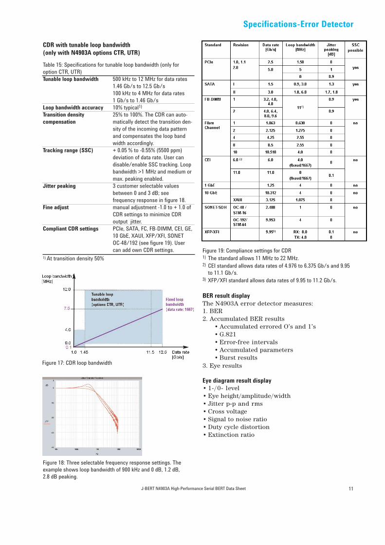
Table 15: Specifications for tunable loop bandwidth (only foroption CTR, UTR)Tunable loop bandwidth 500 kHz to 12 MHz for data rates
1.46 Gb/s to 12.5 Gb/s 100 kHz to 4 MHz for data rates 1 Gb/s to 1.46 Gb/s
Loop bandwidth accuracy 10% typical1)
Transition density 25% to 100%. The CDR can auto-compensation matically detect the transition den-
sity of the incoming data pattern and compensates the loop bandwidth accordingly.
Tracking range (SSC) + 0.05 % to -0.55% (5500 ppm) deviation of data rate. User can disable/enable SSC tracking. Loop bandwidth >1 MHz and medium or max. peaking enabled.
Jitter peaking 3 customer selectable values between 0 and 3 dB; see frequency response in figure 18.
Fine adjust manual adjustment -1.0 to + 1.0 of CDR settings to minimize CDR output jitter.
Compliant CDR settings PCIe, SATA, FC, FB-DIMM, CEI, GE, 10 GbE, XAUI, XFP/XFI, SONET OC-48/192 (see figure 19). User can add own CDR settings.
1) At transition density 50%
J-BERT N4903A High-Performance Serial BERT Data Sheet 11
BER result displayThe N4903A error detector measures:1. BER2. Accumulated BER results
• Accumulated errored O’s and 1’s• G.821• Error-free intervals• Accumulated parameters• Burst results
3. Eye results
Eye diagram result display• 1-/0- level• Eye height/amplitude/width• Jitter p-p and rms• Cross voltage• Signal to noise ratio• Duty cycle distortion• Extinction ratio
Figure 18: Three selectable frequency response settings. Theexample shows loop bandwidth of 900 kHz and 0 dB, 1.2 dB, 2.8 dB peaking.
Specifications-Error Detector
CDR with tunable loop bandwidth (only with N4903A options CTR, UTR)
Figure 19: Compliance settings for CDR1) The standard allows 11 MHz to 22 MHz.2) CEI standard allows data rates of 4.976 to 6.375 Gb/s and 9.95
to 11.1 Gb/s.3) XFP/XFI standard allows data rates of 9.95 to 11.2 Gb/s.
Figure 17: CDR loop bandwidth

12 J-BERT N4903A High-Performance Serial BERT Data Sheet
Table 16: Specifications for trigger outputClock divider 4, 8, 16 up to 11 Gb/s
32, 40, 64, 128 up to 12.5 Gb/sLevels High: +0.5 V typical
Low: --0.5 V typicalMinimum pulse width Pattern length x clock period/2
e.g. 10 Gb/s with 1000 bits = 50nsInterface DC coupled, 50 W nominalConnector SMA female
Table 18: Specifications for the auxiliary outputAmplitude 600 mV typicalInterface AC coupled, 50 W nominalConnector SMA female
Table 19: Specifications for gating inputBurst synchronization time 1536 bits for PRBS
15 kbit for patternBacklash 1536 bits in non-CDR mode
1.5 µs in CDR-modeGate passive time 2560 bits in non-CDR mode
2560 bits or 1.5 µs whichever is longer, in CDR-mode
Interface levels TTL levelsPulse width 256 clock periodsConnector SMA female
Table 17: Specifications for error outputInterface format RZ, active highLevels High: 1 V typical
Low: 0 V typicalPulse width 128 clock periodsInterface DC coupled, 50 W nominalConnector SMA female
Trigger output (TRIG OUT)
Pattern trigger modeThis provides a trigger synchronized with theselected error detector reference pattern. In pat-tern mode the pulse is synchronized to repetitionsof the output pattern. It generates 1 pulse for every4th PRBS pattern.
Divided clock modeIn divided clock mode, the trigger is a square wave.
Error output (ERR OUT)This provides a signal to indicate received errors.The output is the logical 'OR' of errors in a 128 bitsegment of the data.
Auxiliary output (AUX OUT)This output can be used to provide either clock ordata signals:Clock: clock signals from the input or the recov-ered clock signals in CDR mode.Data: weighted and sampled data.
Gating input (GATE IN)If a logical high is applied to the gating input theanalyzer will ignore the incoming bits during aBER measurement. The ignored bit sequence is amultiple of 512 bits. For measuring data in burstsof bits, rather than a continuous stream of bits, aspecial operating mode is used. This is the burstsync mode. In this case, the signal at the gatinginput controls the synchronization and the errorcounting for each burst.
This is an important feature for recirculation loopmeasurements. If clock data recovery (CDR) isused to recover the clock from the burst data, theCDR takes 2 µs from the start of the burst data tosettle. The number of bits needed to synchronizeitself during a burst depends on whether the pat-tern consists of hardware based PRBS data ormemory based data. To run properly in burst modethe system needs a backlash of data after the gat-ing input returns to high. During each burst, thegating input has to remain passive.
Figure 20: Burst mode allows recirculation loop testing.
Pattern capture The error detector can capture up to 32 MB databits from the device under test. The captured databits are displayed in the pattern editor in hex orbinary format. The data bits can be used asexpected data for BER testing or can be saved forpost processing.
Specifications-Error Detector

= UI
Figure 22: Periodic jitter maximum for datarates ~ 3.375 Gb/susing the 500 ps delay line.
J-BERT N4903A High-Performance Serial BERT Data Sheet
Periodic jitter (option J10)This injects sinusoidal, rect-angular or triangular jitter overa wide frequency range.
Jitter Tolerance Test Specifications
The built-in jitter sources cover PCI Express, SATA, Fibre channel, FB-DIMM, CEI 6 G/11 G, 10 GbE and XFP/XFI jitter tolerance test needs. If jitter sources are enabled, the intrinsic jitter atthe pattern generators clock and data outputs is 1.4ps rms typical.
Sinusoidal jitter (option J10)This injects sinusoidal jitter in the lower frequency range withmultiple UIs.
Figure 23: Sinusoidal jitter maximum UI
Figure 21: Periodic jitter maximum for all data rates using the 200 ps delay line.
13
Specifications-Jitter Tolerance Test
Table 20: Specifications for periodic jitter (PJ)Range 1) 0 to 200 ps pp @ all datarates
0 to 500 ps pp @ datarates~ 3.375 Gb/s
Modulation 1 kHz to 300 MHz sinewavefrequency 1 kHz to 20 MHz triangle
1 kHz to 20 MHz square waveModulation frequency 0.5% ± 25 Hz typicalaccuracyJitter amplitude 10% ± 1ps typicalaccuracySignals impacted Data outputs: for all datarates
subrate clock outputs, for datarates ~ 3.375 Gb/s when using 500 ps delay line
1) Available range depends on modulation frequency and data rate(see figure 18 and 19)
Table 21: Specifications for sinusoidal jitter (SJ)Range1) 1000 UI @ 10 kHz
2 UI @ 5 MHzFor frequencies between 10 kHz and 5 MHz the jitter amplitude
10 MHz n x f (mod)
Modulation 100 Hz to 5 MHzfrequency (For higher modulation
frequencies see table 20 and 21.)Modulation frequency 0.5% typicalaccuracyJitter amplitude 2% ± 1ps typicalaccuracySignals impacted Data and subrate clock outputs.
User selectable: all pattern gener-ator outputs (data, clock, subrateclock and trigger outputs.)
1) Available range depends on modulation frequency and data rate(see figure 23).

BUJ calibration datarate for PRBS filtersetting PRBS generatorCEI 6G 1.1 Gb/s PRBS 29-1 100 MHzCEI 11G 2 Gb/s PRBS 211-1 200 MHzGaussian 2 Gb/s PRBS 231-1 100 MHz
Table 23: Specifications for bounded uncorrelated jitter (BUJ)Range 0 to 200 ps pp @ all dataratesPRBS polynomials 2 n-1; n = 7, 8, 9, 10, 11, 15, 23, 31Data rate of PRBS 200 Mb/s to 3.2 Gb/sgeneratorFilters 20/50/100/200 MHz lowpass 3rd orderJitter amplitude 10% ± 1 ps typical for settings shown in accuracy table 24.
Table 24: BUJ accuracy applies for these BUJ calibration settings.
14 J-BERT N4903A High-Performance Serial BERT Data Sheet
Random jitter (option J10)This injects random jitter with ahigh bandwidth and excellent crest factor.
Table 22: Specifications for random jitter (RJ)Range 0 to 14 ps rms Crestfactor 14 (pp to rms ratio)Bandwidth 50 kHz to 1 GHzFilter 10 MHz high-pass
500 MHz low-pass Can be turned on/off individually to limit jitter bandwidth.
Jitter amplitude 10% ± 0.2 ps typicalaccuracy
Note: Other settings are not calibrated and do not neces-sarily generate the desired jitter histograms for alldatarates of the PRBS generator.
Figure 24: Overview of jitter injection capabilities
Total jitterA combination of internally generated PJ, RJ, BUJand external jitter (injected using external delaycontrol input) is possible:For all datarates: RJ + PJ + BUJ + external delaycontrol input: total delay variation is 200 ps pp max. For datarates ~ 3.375 Gb/s: A 200 ps delay lineor a 500 ps delay line can be used. If the 500 ps delay line is used: only PJ or only SJor only SSC can be injected.Total delay variation for periodic jitter is shown infigure 21.Total delay variation is 200 ps max. for RJ + exter-nal delay control input.
Bounded uncorrelated jitter (option J10)This injects a high probabilityjitter using a PRBS generatorand low-pass filters.
Specifications-Jitter Tolerance Test
[1]: When 500ps delay line is used for PJ, additional SSC,SJ and BUJ is not available. The 200ps delay can be used inaddition, see above for maximum available total jitter.
[2]: When using Automated Characterization/ Compliance:sinusoidal jitter sweep is generated by SJ and PJ (200 psdelay line). Additional PJ or SJ cannot be injected. SSC canbe enabled (requires SW rev. 4.5 or later). With SSCenabled only PJ (200ps delay line) is used for jitter sweep.
[3]: When using CLK IN (external) SSC, SJ and 500 ps delayline are not available. It is possible to inject a modulatedexternal clock which must not exceed J-BERT‘s built-in jit-ter injection capabilities for SSC/SJ or the 500 ps delayline.

Table 26: Specifications for sinusoidal interference (SI)Amplitude 1) 0 to 400 mV common mode, single
ended and differential (differential amplitude 0 to 800 mV)
Frequency 10 MHz to 3.2 GHz in 100 kHz stepsLevel accuracy ± 10% ±10 mV typical
1) The output signal amplitude is reduced by 3 dB when sinusoidalinterference is enabled.
Figure 26: Typical S21 parameter for ISI channel of 9 inch length.
Table 25: Specifications for intersymbol interference (ISI)
Sinusoidal interference (option J20)This adds common mode, dif-ferential or single-endedsinewave signal on top of thedata outputs, to test commonmode rejection of a receiver andto emulate vertical eye closure.
Sinusoidal interference is injected before the sig-nal passes through the ISI board traces (“nearend”) when using P1 as input. For “far end” injec-tion P2 has to be used as input.
J-BERT N4903A High-Performance Serial BERT Data Sheet
Figure 25: Interference channel connectors
Interference channel (option J20)The option J20 is only available in addition tooption J10. It includes semi-rigid cable set to connect data outputs to P1 and P1 (N4915A-002).
Interference channel input and output (P1, P2)User selectable board traces areswitched into the signal path toemulate a backplane.
Figure 27: Typical ISI (measured in UI) for traces depending on datarate, pattern and trace length.
Trace length 3.5” (minimum), 9” (minimum with S.I. enabled) 16”, 20”, 24”, 28”, 32”, 36”, 40”, 44” inches of board trace type Nelco 4000-6. When using in combination with sinusoidal interfer-ence, minimum trace length is 9 inches.
S21 parameter See figure 26Range See figure 27Max. input levels -- 5 .5 V to +5.5 VConnectors 2.4 mm, female
15
Specifications-Jitter Tolerance Test

J-BERT N4903A High-Performance Serial BERT Data Sheet
Table 27: General mainframe characteristics
Figure 28: Rear panel view
Display8" color LCD touch screen
Data entry• Color touch screen display, numeric keypad
with up/down arrows, dial-knob control or external key board and mouse via USB interface
• Pattern export/import
Hard diskFor local storage of user patterns and data. Anexternal disk is also available for using over theUSB interface.
Removable storageFloppy Disk Drive 1.44 MB
Remote control interfacesGPIB (IEEE 488), LAN, USB 2.0.Language: SCPI, IVI.COM. SCPI commands can beexported via copy/paste from the utility menu/out-put window.Built-in web server: provides remote GUI accessand control of J-BERT via a standard Java enabledweb browser on your computer. (Requires SW 4.5or higher.)
IO librariesAgilents IO libraries suite ships with the N4903A tohelp quickly establish an error-free connectionbetween your PC and instruments regardless of thevendor.
Other interfacesParallel printer port, 2 x LAN, VGA output, 4 xUSB2.0, 1x USB 1.1 (front).
Operating systemMicrosoft Windows XP Professional
Regulatory standardsSafety: IEC 61010-1:2001
EN 61010-1:2001CAN/CSA-C22.2 No.61010-1-04UL 61010-1:2004
EMC: EN 61326:1997 + A1:1998 + A2:2001IEC 61326:1997 + A1:1998 + A2:2000
Quality management: ISO 9004
Specification assumptionThe specifications in this brochure describe theinstrument’s warranted performance. Non-war-ranted values are described as typical.All specifications are valid in a range from 5 °C to40 °C ambient temperature after a warm-up phaseof 30 minutes. If not otherwise stated, all inputsand outputs need to be terminated with 50 Ω toground. All specifications, if not otherwise stated,are valid using the recommended cable set N4910A(2.4 mm, 24” matched pair).
16
Mainframe Characteristics
Operating temperature 5°C to 40 °CStorage temperature - 40°C to +70°COperating humidity 95% rel. humidity,
non-condensingStorage humidity 50% rel. humidityPower requirements 100 to 240 V, ±10%,
47 to 63 Hz, 450 VAPhysical dimensions Width: 424.5 mm
Height: 221.5 mmDepth: 580.0 mm
Weight (net) 26 kg Weight (shipping) (max) 37.5 kgRecommended 1 yearre-calibration periodWarranty period 1 year return to Agilent.
See order instructions for extended warranty.

J-BERT N4903A High-Performance Serial BERT Includes 5x 50 Ω SMA terminations, 6x adapter SMAfemale to 2.4 mm male, USB cable, commercial cali-bration report and certificate (“UK6”), getting start-ed guide, Agilent I/O library.
BERT pattern generator and error detectorwith built-in CDRBERT 150 Mb/s to 12.5 Gb/s N4903A-C13BERT 150 Mb/s to 7 Gb/s N4903A-C07
Pattern generator (PG) capabilities*Only with opt. J10SSC generation* N4903A- J11PG 150 Mb/s to 12.5 Mb/s* N4903A-G13PG 150 Mb/s to 7 Gb/s* N4903A-G07
Analyzer capabilitiesBit recovery mode N4903A-A01Tunable loop bandwidth CDR N4903A-CTR
Jitter tolerance optionsRJ, PJ, SJ, BUJ injection N4903A-J10Interference channel N4903A-J20(Includes short cable kit N4915A-002)Jitter tolerance compliance suite N4903A-J12 (Only with opt. J10)
Upgrades N4903AUFrom BERT 7 Gb/s (opt. C07) N4903A-U13to BERT 12.5 Gb/s (opt. C13) To bit recovery mode -A01 N4903A-U01To jitter tolerance -J10 N4903A-U10(Requires recalibration at Agilent) To SSC -J11 N4903A-U11To interference channel -J20 N4903A-J20To jitter compliance -J12 N4903A-U12To CDR with tunable N4903A-UTRloop bandwidth -CTRFrom pattern generator 12.5 Gb/s N4903A-UED(opt. G13) to BERT 12.5 Gb/s(opt. C13)From pattern generator 7 Gb/s N4903A-UE7(opt. G07) to BERT 7 Gb/s(opt. C07)
WarrantyExtended warranty R1280A
CalibrationCalibration services R1282ACommercial calibration (N4903A-UK6)with test data is always included
Productivity assistanceRemote or on-site R1380-N49xxProductivity assistance PS-S20 and
PS-S20-02
J-BERT N4903A High-Performance Serial BERT Data Sheet
Recommended accessories2.4 mm cable kit N4910ADe-emphasis signal converter N4916ARack mount kit N4914A-FGOne 47 ps transition time N4915A-001converterOne adaptor 3.5 mm female N4911A-002to 2.4 mm male50 W terminations, 2.4 mm N4912AShort cable kit, N4915A-0022.4 mm (m) to 2.4 mm (m) for ISI ports
Figure 29: Clock cable N4915A-003
Figure 30: Short cable kit for connecting ISI ports. N4915A-002.
17
Order Instructions

® PCI Express is a registered trademark of PCI-SIG.
Remove all doubt
Our repair and calibration services will get your equipment backto you, performing like new, when promised. You will get fullvalue out of your Agilent equipment throughout its lifetime. Yourequipment will be serviced by Agilent-trained technicians usingthe latest factory calibration procedures, automated repair diag-nostics and genuine parts. You will always have the utmost con-fidence in your measurements.
Agilent offers a wide range of additional expert test and meas-urement services for your equipment, including initial start-upassistance onsite education and training, as well as design, sys-tem integration, and project management.
For more information on repair and calibration services, go to:
www.agilent.com/find/removealldoubt
www.agilent.com
For more information on Agilent Technologies’ products, applica-tions or services, please contact your local Agilent office. Thecomplete list is available at:
www.agilent.com/find/contactus
Phone or Fax
United States: China:(tel) 800 829 4444 (tel) 800 810 0189(fax) 800 829 4433 (fax) 800 820 2816Europe: Japan:(tel) 31 20 547 2111 (tel) (81) 426 56 7832Korea: (fax) (81) 426 56 7840(tel) (080) 769 0800 Latin America:(fax) (080) 769 0900 (tel) (305) 269 7500Other Asia Pacific Countries: Taiwan:(tel) (65) 6375 8100 (tel) 0800 047 866(fax) (65) 6755 0042 (fax) 0800 286 331
Email: [email protected]
Revised: 09/14/06
© Agilent Technologies, Inc. 2007, 2005Printed in USA, January 18, 2007
5989-2899EN
If you want to learn more about jitter, please visit our website:www.agilent.com/find/jittermaster
www.agilent.com/find/emailupdatesGet the latest information on the products and applications youselect.
Related Literature Pub. No.
J-BERT N4903A High-Performance Serial BERT 5989-3882ENBrochure
Bit Recovery Mode for characterizing idle 5989-3796ENand framed data traffic Application Note
Calibrated Jitter, Jitter Tolerance Test and Jitter 5989-4967ENLaboratory with the J-BERT N4903AApplication Note
Mastering jitter characterization with J-BERT & DCA-J 5989-4823ENPoster
Second Generation PCI EXPRESS® Testing 5989-4087ENwith the N4903A High-Performance Serial BERTApplication Note
N4906B Serial BERT 3 and 12.5 Gb/s 5989-2406ENData sheet
Agilent Physical Layer Test 5988-9514ENBrochure
ParBERT 81250 5968-9188EProduct Overview
86100 Infiniium DCA-J 5989-0278ENData Sheet
Infiniium 80000 Series 5989-1487ENUS Oscilloscopes Data Sheet
Fast Total Jitter Solution 5989-3151ENApplication Note
N5990A Test Automation Software Platform 5989-5483ENData Sheet
De-Emphasis Signal Converter 5989-6062ENData Sheet
www.agilent.com/find/j-bert
Product specifications and descriptions in this documentare subject to change without notice.
For the latest version of this document, please visit our website atwww.agilent.com/find/j-bert and go to the Key LibraryInformation and insert the publication number (5989-2899EN) intothe search engine.
www.agilent.com/find/agilentdirectQuickly choose and use your test equipment solutions with confidence.
www.agilent.com/find/openAgilent Open simplifies the process of connecting and program-ming test systems to help engineers design, validate and manufac-ture electronic products. Agilent offers open connectivity for abroad range of system-ready instruments, open industry software,PC-standard I/O and global support, which are combined to moreeasily integrate test system development.