Embed Size (px)
Citation preview

Agilent ADNS-2610Optical Mouse SensorData Sheet
DescriptionThe ADNS-2610 is a new entrylevel, small form factor opticalmouse sensor. It is used toimplement a non-mechanicaltracking engine for computermice. Unlike its predecessor, thisnew optical mouse sensor allowsfor more compact and affordableoptical mice designs.
It is based on optical navigationtechnology, which measureschanges in position by opticallyacquiring sequential surfaceimages (frames) and mathemati-cally determining the directionand magnitude of movement.
The sensor is housed in an8-pin staggered dual inlinepackage (DIP). It is designed foruse with the HDNS-2100 Lens,HLMP-ED80-XXXXX, and theHDNS-2200 LED Clip, providingan optical mouse solution that iscompact and affordable. Thereare no moving parts, so precisionoptical alignment is not required,thereby facilitating high volumeassembly.
The output format is a two wireserial port. The current X and Yinformation are available inregisters accessed via the serialport.
Resolution is 400 counts per inch(cpi) with rates of motion up to12 inches per second (ips).
Theory of OperationThe ADNS-2610 is based onOptical Navigation Technology. Itcontains an Image AcquisitionSystem (IAS), a Digital SignalProcessor (DSP) and a two wireserial port.
The IAS acquires microscopicsurface images via the lens andillumination system provided bythe HDNS-2100, HDNS-2200, andHLMP-ED80-XXXXX. Theseimages are processed by the DSPto determine the direction anddistance of motion.
Features• Precise optical navigation technology
• Small form factor(10 mm x 12.5 mm footprint)
• No mechanical moving parts
• Complete 2D motion sensor
• Common interface for generalpurpose controller
• Smooth surface navigation
• Accurate motion up to 12 ips
• 400 cpi resolution
• High reliability
• High speed motion detector
• Wave solderable
• Single 5.0 volt power supply
• Conforms to USB suspend modespecifications
• Power conservation mode duringtimes of no movement
• Serial port registers– Programming– Data transfer
• 8-pin staggered dual inlinepackage (DIP)
Applications• Mice for desktop PC’s,
workstations, and portable PC’s
• Trackballs
• Integrated input devices
2
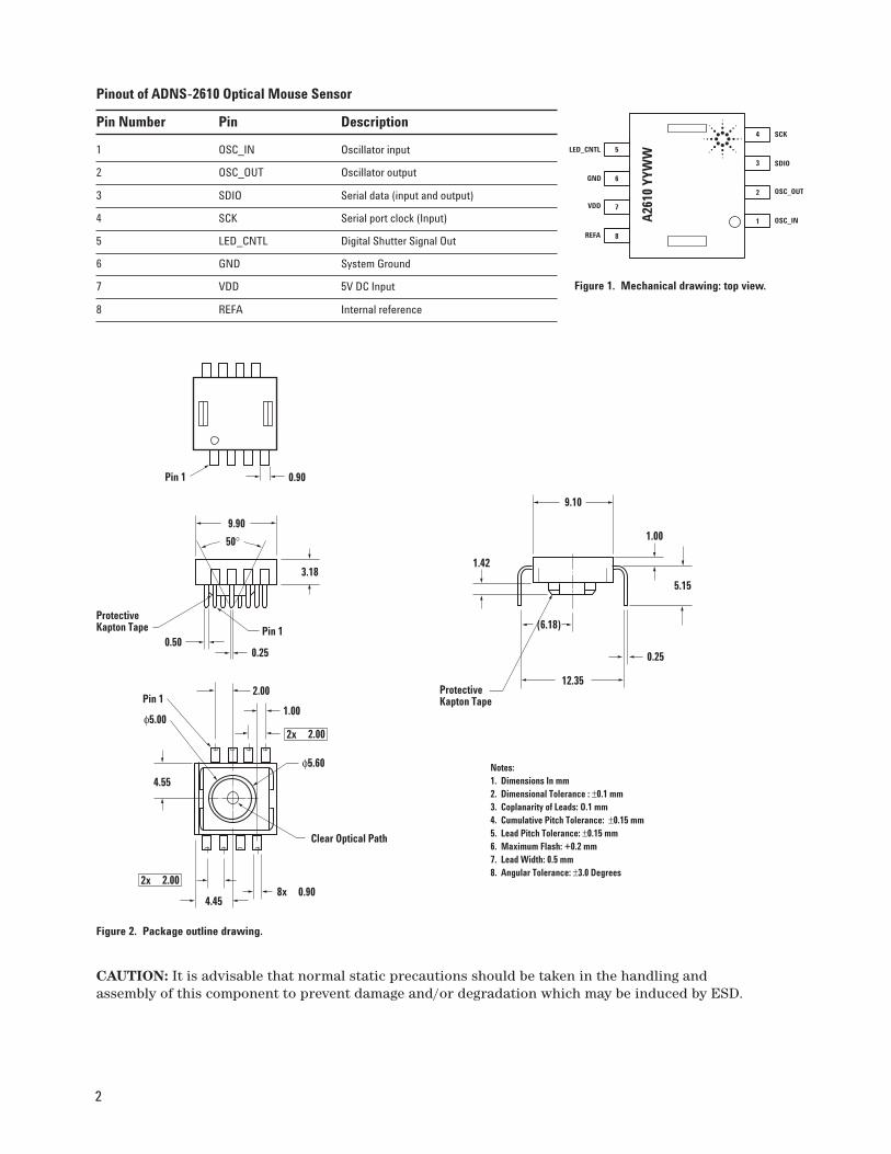
Pinout of ADNS-2610 Optical Mouse Sensor
Pin Number Pin Description
1 OSC_IN Oscillator input
2 OSC_OUT Oscillator output
3 SDIO Serial data (input and output)
4 SCK Serial port clock (Input)
5 LED_CNTL Digital Shutter Signal Out
6 GND System Ground
7 VDD 5V DC Input
8 REFA Internal reference
Figure 2. Package outline drawing.
Figure 1. Mechanical drawing: top view.
5
6
7
8
LED_CNTL
GND
VDD
REFA
SCK
SDIO
OSC_OUT
OSC_IN
4
3
2
1A26
10 Y
YWW
Pin 1
Notes:1. Dimensions In mm2. Dimensional Tolerance : ±0.1 mm3. Coplanarity of Leads: O.1 mm4. Cumulative Pitch Tolerance: ±0.15 mm5. Lead Pitch Tolerance: ±0.15 mm6. Maximum Flash: +0.2 mm7. Lead Width: 0.5 mm8. Angular Tolerance: ±3.0 Degrees
0.90
Pin 1ProtectiveKapton Tape
0.500.25
2.00
1.00
2x 2.00
φ5.60
Clear Optical Path
φ5.00
Pin 1
9.90
3.18
50°
0.25
12.35ProtectiveKapton Tape
(6.18)
9.10
1.00
5.15
1.42
4.55
4.450.908x
2x 2.00
CAUTION: It is advisable that normal static precautions should be taken in the handling andassembly of this component to prevent damage and/or degradation which may be induced by ESD.

3
Overview of Optical MouseSensor AssemblyNOTE: Pin 1 of optical mousesensor should be inserted intothe reference point of mechanicalcutouts.
Figures 3 and 4 are shown withHDNS-2100, HDNS-2200 andHLMP-ED80-XXXXX.
Agilent Technologies provides anIGES file drawing describing thebase plate molding features forlens and PCB alignment.
The components shown in Figure5 interlock as they are mountedonto defined features on the baseplate.
The ADNS-2610 sensor is de-signed for mounting on a throughhole PCB, looking down. There isan aperture stop and features onthe package that align to the lens.
The HDNS-2100 lens providesoptics for the imaging of thesurface as well as illumination ofthe surface at the optimum angle.Features on the lens align it tothe sensor, base plate, and clipwith the LED. The lens also has alarge round flange to provide along creepage path for any ESDevents that occur at the openingof the base plate.
The HDNS-2200 clip holds theLED in relation to the lens. TheLED’s leads must be formed firstbefore inserting into the clip.Then, both LED and clip isloaded on the PCB. The clipinterlocks the sensor to the lens,and through the lens to thealignment features on the baseplate.
The HLMP-ED80-XXXXX isrecommended for illumination. Ifused with the bin table (as shownin Figure 8), sufficient illumina-tion can be guaranteed.
Figure 5. Exploded view drawing.
Figure 3. Recommended PCB mechanical cutouts and spacing.
HDNS-2200 (Clip)
HLMP-ED80-XXXXX
ADNS-2610 (Sensor)
Customer supplied PCB
HDNS-2100 (Lens)
Customer supplied base platewith recommended alignment features per IGES drawing
Figure 4. 2D assembly drawing of ADNS-2610 shown with the HLMP-ED80 (top and side view).
BASE PLATE
PLASTIC SPRINGCLIP
BASE PLATE ALIGNMENT POSTSENSORPCB
ESD LENS RING
7.450.293
32.461.278
19.100.752
13.820.544
10.580.417
14.580.574
Dimensions in mm/in.
+X
+Y
(Top view)
(Side view)
φ
29.15
CLEAR ZONE
ALL DIMENSIONS0 ref
1.148
10.420.410
12.350.486
1.93.076
MMINCH
1.34.053
4.98.196
7.38.291
13.760.542
3.50.138
28.011.103
18.940.7461.00
.039
9.06.357
0 ref

4
PCB Assembly Considerations1. Insert the sensor and all other
electrical components intoPCB. Note: Pin 1 of the sensorshould always be the referencepoint of mechanical cutouts.
2. Bend the LED leads 90° andthen insert the LED into theassembly clip until the snapfeature locks the LED base.
3. Insert the LED/clip assemblyinto PCB.
4. Wave solder the entire assem-bly in a no-wash solderprocess utilizing solderfixture. The solder fixture isneeded to protect the sensorduring the solder process. Thefixture should be designed toexpose the sensor leads tosolder while shielding the
Figure 6. Block diagram of ADNS-2610 optical mouse sensor.
7. Insert PCB assembly over thelens onto the base platealigning post to retain PCBassembly. The sensor aperturering should self-align to thelens.
8. The optical position referencefor the PCB is set by the baseplate and lens. Note that thePCB motion due to buttonpresses must be minimized tomaintain optical alignment.
9. Install mouse top case. ThereMUST be a feature in the topcase to press down onto theclip to ensure all componentsare interlocked to the correctvertical height.
Design Considerations for ImprovingESD PerformanceThe flange on the lens has beendesigned to increase the creepageand clearance distance forelectrostatic discharge. The tablebelow shows typical valuesassuming base plate constructionper the Agilent supplied IGES fileand HDNS-2100 lens flange.
Typical Distance Millimeters
Creepage 16.0
Clearance 2.1
For improved ESD performance,the lens flange can be sealed (i.e.glued) to the base plate. Notethat the lens material is polycar-bonate and therefore, cyanoacry-late based adhesives or otheradhesives that may damage thelens should NOT be used.
optical aperture from directsolder contact. The solderfixture is also used to set thereference height of the sensorto the PCB top during wavesoldering (Note: DO NOTremove the kapton tape duringwave soldering).
5. Place the lens onto the baseplate.
6. Remove the protective kaptontape from optical aperture ofthe sensor. Care must be takento keep contaminants fromentering the aperture. It isrecommended not to place thePCB facing up during theentire mouse assembly pro-cess. The PCB should be heldvertically for the kaptonremoval process.
SCK
SDIO
SERIALPORT
SERIAL PORT
IMAGE PROCESSOR
LED CONTROL
LED CONTROL
OSCILLATOR RESONATOR
OSC_IN
OSC_OUT
REFA
VOLT
AG
E R
EGU
LATO
RA
ND
PO
WER
CO
NTR
OL
VDD
GND
VOLTAGE REFERENCE
5 VOLT POWER
PCB
Sensor
LED
Base Plate
Lens/Light Pipe
Clip
Surface
Figure 7. Sectional view of PCB assembly highlighting optical mouse components (optical mouse sensor, clip, lens, LED, PCB and base plate).

5
Figure 8. Circuit block diagram for a typical corded optical mouse using an Agilent ADNS-2610 optical mouse sensor.
6 MHz
(Optional)
10 9
P0.7
P0.6
XTALINXTALOUT
D+
D-
Vreg
P1.0
P1.1
P0.0
Vpp
VDD
GND
VDD
SDIO
SCK
LED_CNTL
SURFACE
1K ohms
100K ohms
R1
2N3906
HDNS2100Lens
InternalImageSensor
HLMP-ED80-XXXXX
OSC_IN Ceramic Resonaator
AVXKBR-24.0-MSA
MurataCSAL24M0X040
2.2 µF
24MHz
OSC_OUT
REFA
7
13
8
5
14
1
12
VDD
D+
D-
GND
GND
1.3 KΩ
0.1 µF 4.7 µF 0.1 µF
QA
QBVDD
R Ω
Z LED
SHLDVDD
11
VSS
CYP
RES
SC
Y7C
6372
3C-P
C
AD
NS-
2610
P0.517
6 5
1
2
8
7
3
4
16
15
P0.3
P0.2
P0.1
4
3
2
6
L
M
R
Buttons
R1 VALUE(Ohms)69.869.869.869.869.8 to 78.769.8 to 93.169.8 to 11369.8 to 13769.8 to 169
KLMNPQRST
LEDBIN
Notes on Bypass 6, 7 and 6, 8Capacitors• Caps for pins 6,7 and 8 to
ground MUST have tracelengths LESS than 5 mm.
• The 0.1 uF caps must beceramic.
• Caps should have less than5 nH of self inductance
• Caps should have less than0.2 ohms ESR
• Surface mount parts arerecommended
Regulatory Requirements• Passes FCC B and worldwide
analogous emission limits whenassembled into a mouse withunshielded cable and followingAgilent recommendations.
• Passes EN61000-4-4/IEC801-4EFTB tests when assembledinto a mouse with shieldedcable and following Agilentrecommendations.
• UL flammability level UL94 V-0.
• Provides sufficient ESDcreepage/clearance distance toavoid discharge up to 15kVwhen assembled into a mouseaccording to usage instruc-tions above.
• For eye safety consideration,please refer to the technicalreport available on the website at www.agilent.com/semiconductors.

6
Absolute Maximum Ratings
Parameter Symbol Minimum Maximum Units Notes
Storage Temperature TS -40 85 °C
Operating Temperature TA -15 55 °C
Lead Solder Temp 260 °C For 10 seconds, 1.6 mm below seating plane
Supply Voltage VDD -0.5 5.5 V
ESD 2 KV All pins, human body model MIL 883 Method 3015
Input Voltage VIN -0.5 VDD+ 0.5 V SDIO, CLK, LED_CNTL
Input Voltage VIN -0.5 3.6 V OSC_IN, OSC_OUT, REFA
Recommended Operating Conditions
Parameter Symbol Minimum Typical Maximum Units Notes
Operating Temperature TA 0 40 °C
Power Supply Voltage VDD 4.1 5.0 5.5 Volts Register values retained for voltagetransients below 4.10V but greaterthan 3.9V
Power Supply Rise Time VRT 100 ms
Supply Noise VN 100 mV Peak to peak within 0-100 MHzbandwidth
Clock Frequency fCLK 23.0 24.0 25.0 MHz Set by ceramic resonator
Serial Port Clock Frequency SCLK fCLK/12 MHz
Resonator Impedance XRES 55 Ω
Distance from Lens Reference Z 2.3 2.4 2.5 mm Results in ±0.2 mm DOFPlane to Surface (See Figure 9)
Speed S 0 12 in/sec @ frame rate = 1500 fps
Acceleration A 0.25 g @ frame rate = 1500 fps
Light Level onto IC IRRINC 80 25,000 mW/m2 λ = 639 nm100 30,000 λ = 875 nm
SDIO Read Hold Time tHOLD 100 µs Hold time for valid data(Refer to Figure 22)
SDIO Serial Write-write Time tSWW 100 µs Time between two write commands(Refer to Figure 25)
SDIO Serial Write-read Time tSWR 100 µs Time between write and readoperation (Refer to Figure 26)
SDIO Serial Read-write Time tSRW 250 ns Time between read and writeoperation (Refer to Figure 27)
SDIO Serial Read-read Time tSRR 250 ns Time between two read commands(Refer to Figure 26)
Data Delay after PD deactivated tCOMPUTE 3.1 ms After tCOMPUTE, all registers containdata from first image after wakeupfrom Power-Down mode. Note that anadditional 75 frames for AGCstabilization may be required if mousemovement occurred while PowerDown. (Refer to Figure 10)
SDIO Write Setup Time tSETUP 60 ns Data valid time before the rising ofSCLK (Refer to Figure 20)
Frame Rate FR 1500 frames/s

7
Figure 9. Distance from lens reference plane to surface.
AC Electrical SpecificationsElectrical Characteristics over recommended operating conditions. Typical values at 25°C, VDD = 5 V, 24 MHz, 1500 fps.
Parameter Symbol Min. Typ. Max. Units Notes
Power Down (PD) tPD
1.33 µs 32 clock cycle minimum after setting bit 6 in theConfiguration register. (refer to Figure 12)
Power Up after PD mode tPUPD 50 ms From PD mode deactivation to accurate reportsdeactivated 610 µs + 75 frames (Refer to Figure 10).
Power Up from VDD ↑ tPU 40 ms From VDD to valid accurate reports610 µs + 50 frames
Rise and Fall Times
SDIO tr 30 ns CL = 30 pF (the rise time is between 10% to 90%)
tf 16 ns CL = 30 pF (the fall time is between 10% to 90%)
Serial Port Transaction Timer tSPTT 90 ms Serial port will reset if current transaction is notcomplete within tSPTT (Refer to Figure 29).
Transient Supply Current IDDT 20 37 mA Max supply current during a VDD ramp from 0 to 5.0Vwith > 500 ms rise time. Does not include chargingcurrent for bypass capacitors.
ADNS-2610
HDNS-2100
Z
OBJECT SURFACE

8
DC Electrical SpecificationsElectrical Characteristics over recommended operating conditions. Typical values at 25°C, VDD = 5 V, 24 MHz, 1500 fps.
Parameter Symbol Min. Typ. Max. Units Notes
Supply Current (mouse moving) IDD AVG 15 30 mA
Supply Current (mouse not moving) IDD 12 mA
Power Down Mode Current IDDPD 170 230 µA
SCK pin
Input Low Voltage VIL 0.8 V
Input High Voltage VIH 2.0 V
Input Capacitance CIN 10 pF
Input Resistance RIN 1 MΩ
SDIO pin VDD = 4V, Load = 50 pF, 80 ns rise & fall
Input Low Voltage VIL 0.8 V
Input High Voltage VIH 2.0 V
Output Low Voltage VOL 0.5 V
Output High Voltage VOH 0.8 * VDD V
Drive Low Current IL 2.0 mA
Drive High Current IH 2.0 mA
Input Capacitance CIN 10 pF
Input Resistance RIN 1 MΩ
LED_CNTL pin
Output Low Voltage VOL 0.1 V
Output High Voltage VOH 0.8 * VDD V
Drive Low Current IL 250 µA
Drive High Current IH 250 µA
OSC_IN
Input Resistance RIN 500 kΩ
Input Capacitance CIN 15 pF
Input High Voltage VIH 2.2 V External clock source
Input Low Voltage VIL 0.8 V External clock source

9
PD Pin TimingNote: All timing circuits shown, from Figure 10onwards, are based on the 24 MHz resonatorfrequency.
Figure 10. Power up timing mode.
Figure 11. Details of wake-up timing after PD.
IDD
Power DownDeactivation
Power Down deactivated
(610) µs
tCOMPUTE (See Figure 11)
t pupd
75 frames
LEDCURRENT
OscillatorStart
Power DownDeactivation
Power Down deactivated
250 µs
ResetCount
360 µs
Initialization New Acquisition
2410 µs
SCK
Optional SPI transactionswith old image data
610 µs
tcompute
SPI transactionswith new image data
At default frame rate

10
Power-down Mode (PD) and TimingADNS-2610 can be placed in apower-down mode by setting bit 6in the configuration register via aserial I/O port write operation.Note that while writing a “1” tobit 6 of the configuration register,all other bits must be writtenwith their original value in orderto keep the current configuration.After setting the configurationregister, wait at least 32 systemclock cycles. To get the chip out
of the power-down mode, clear bit6 in the configuration register viaa serial I/O port write operation.(CAUTION! In power-down mode,the SPI timeout (t
SPTT) will not
function. Therefore, no partialSPI command should be sent.Otherwise, the sensor may gointo a hang-up state). While thesensor is in power-down mode,only the bit 6 data will be writtento the configuration register.
Writing the other configurationregister values will not have anyeffect. For an accurate reportafter power-up, wait for a totalperiod of 50 ms before themicrocontroller is able to issueany write/read operation to theADNS-2610. The sensor registersettings, prior to power-downmode, will remain during power-down mode.
Figure 13. Power-down configuration register writing operation.
Setting the power down bitsimply sets the analog circuitryinto a no current state.
Note: LED_CNTL, and SDIO willbe tri-stated during power downmode.
Figure 12. Power-down timing.
The address of the configurationregister is 0000000. Assume thatthe original content of theconfiguration register is 0x00.
CLK
SCK
SDIO
IDD
32 clock cycles min
1 A6 A5 A4 A3 D5 D4 D3 D2 D1 D0
tPD
Configuration Register Address
1 0 0 0 0 0 0 0 0 0 0 0 0 0 01
Configuration Register DataWrite
SCK
SDIO
Operation

11
Typical Performance CharacteristicsPerformance characteristics over recommended operating conditions. Typical values at 25°C, VDD = 5 V, 24 MHz, 1500 fps.
Parameter Symbol Min. Typ. Max. Units Notes
Path Error (Deviation) PError 0.5 % Path Error (Deviation) is the error from the ideal cursor path. It is expressedas a percentage of total travel and is measured over standard surfaces.
The following graphs(Figures 14-18)are the typicalperformance of the ADNS-2610sensor, assembled as shown inthe 2D assembly drawing withthe HDNS-2100 Lens/Prism, theHDNS-2200 clip, and theHLMP-ED80-XXXXX(See Figure 4).
z (mm)
Figure 14. Typical Resolution vs. Z (comparative surfaces)
DPI
-1
500
400
300
200
100
0-0.8 -0.6 -0.4 -0.2 -0 0.2 0.4 0.6 0.8 1
Burl FormicaWhite PaperManilaBlack CopyBlack Walnut
VELOCITY (ips)
Figure 15. Typical Resolution vs. Velocity @ 1500 fps.
DPI
1
500
400
300
200
100
03 5 7 9 11 13 15
White PaperManilaBlack Copy
WAVELENGTH (nm)
REL
ATI
VE R
ESPO
NSE
400 1000700500 900800600
1.0
0.8
0.6
0.4
0.2
0
Figure 16. Wavelength Responsivity[1].
Notes:1. The ADNS-2610 is designed for optimal
performance when used with theHLMP-ED80-XXXXX(red LED 639 nm). For usewith other LED colors (i.e., blue, green),please consult factory. When using alternateLEDs, there may also be performancedegradation and additional eye safetyconsiderations.
2. Z = Distance from Lens Reference plane toSurface.
3. DOF = Depth of Field.
z (mm)
Figure 17. Typical Resolution vs. Height at different LED current levels on manila folder.
DPI
-1
500
400
300
200
100
0-0.6 -0.2 0.2 0.6 1
100%75%50%
z (mm)
Figure 18. Typical Resolution vs. Height at different LED current levels on black copy.
DPI
-1
600
500
400
300
200
100
0-0.6 -0.2 0.2 0.6 1
100%75%50%

12
Figure 19. Write operation.
Synchronous Serial PortThe synchronous serial port isused to set and read parametersin the ADNS-2610, and also toread out the motion information.
The port is a two wire, halfduplex port. The hostmicrocontroller always initiatescommunication; the ADNS-2610never initiates data transfers.
SCK: The serial port clock. It isalways generated by the master(the microcontroller).
SDIO: The data line.
Write OperationWrite operations, where data isgoing from the microcontroller tothe ADNS-2610, is always initi-ated by the microcontroller and
consists of two bytes. The firstbyte contains the address (sevenbits) and has a “1” as its MSB toindicate data direction. Thesecond byte contains the data.The transfer is synchronized bySCK. The microcontrollerchanges SDIO on falling edges ofSCK. The ADNS-2610 readsSDIO on rising edges of SCK.
SCK
SDIO
SDIO Driven by Microcontroller
1 A6 A5 A4 A3 A2 A1 A0 D7 D6 D5 D4 D3 D2 D1 D0
1 2 3 4 5 6 7 8 9 10 11 12 13 14 15 16SCK
Cycle #
DON'TCARE
Figure 20. SDIO setup and hold times SCK pulse width.
SCK
SDIO
tsetup = 60 ns, min
250 ns, min
250 ns 250 ns

13
NOTE:The 250 ns high state of SCK is the minimumdata hold time of the ADNS-2610. Since thefalling edge of SCK is actually the start of thenext read or write command, the ADNS-2610 willhold the state of D0 on the SDIO line until thefalling edge of SCK. In both write and readoperations, SCK is driven by the microcontroller.
Read OperationA read operation, meaning datathat is going from the ADNS-2610to the microcontroller, is alwaysinitiated by the microcontrollerand consists of two bytes. Thefirst byte that contains theaddress is written by themicrocontroller and has a “0” asits MSB to indicate data direc-
tion. The second byte containsthe data and is driven by theADNS-2610. The transfer issynchronized by SCK. SDIO ischanged on falling edges of SCKand read on every rising edge ofSCK. The microcontroller mustgo to a High-Z state after the lastaddress data bit. The ADNS-2610will go to the High-Z state after
the last data bit. Another thing tonote during a read operation;SCK needs to be delayed after thelast address data bit to ensurethat the ADNS-2610 has at least100 µs to prepare the requesteddata. This is shown in the timingdiagrams below (See Figures 21to 23).
Figure 21. Read operation.
SDIO Driven by Microcontroller SDIO Driven by ADNS-2610
1 2 3 4 5 6 7 8SCK
Cycle #
SCK
SDIO 0 A 6 A 5 A 4 A 3 A 2 A 1 A 0 D6 D5 D4 D3 D2 D1 D0D7
9 10 11 12 13 14 15 16
Detail "A" Detail "B"
250 ns, max
Microcontrollerto ADNS-2610SDIO handoff
Detail "A"
A 0
250 ns, min
SCK
SDIO Hi-Z
0 ns, min
A 1
250 ns, max
D 7
160 ns, min
D 6
60 ns, min
t HOLD
100 µs, min
ADNS-2610 toMicrocontrollerSDIO handoff
Detail "B"
SCK
SDIO
250 ns, min
D0
160 ns, max
R/W bit of next address
Released by ADNS-2610 Driven by microcontroller
Figure 22. Microcontroller to ADNS-2610 SDIO handoff.
Figure 23. ADNS-2610 to microcontroller SDIO handoff.
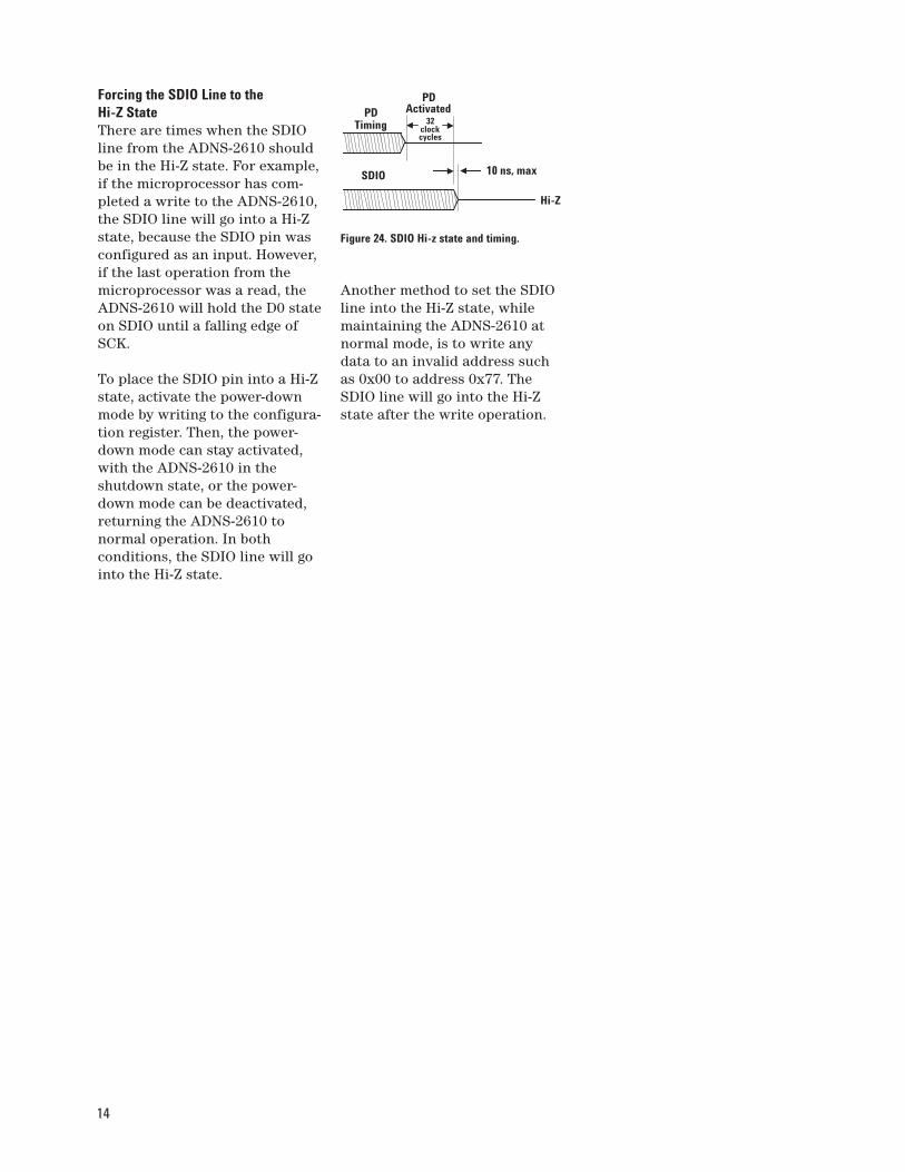
14
Figure 24. SDIO Hi-z state and timing.
Forcing the SDIO Line to theHi-Z StateThere are times when the SDIOline from the ADNS-2610 shouldbe in the Hi-Z state. For example,if the microprocessor has com-pleted a write to the ADNS-2610,the SDIO line will go into a Hi-Zstate, because the SDIO pin wasconfigured as an input. However,if the last operation from themicroprocessor was a read, theADNS-2610 will hold the D0 stateon SDIO until a falling edge ofSCK.
To place the SDIO pin into a Hi-Zstate, activate the power-downmode by writing to the configura-tion register. Then, the power-down mode can stay activated,with the ADNS-2610 in theshutdown state, or the power-down mode can be deactivated,returning the ADNS-2610 tonormal operation. In bothconditions, the SDIO line will gointo the Hi-Z state.
Another method to set the SDIOline into the Hi-Z state, whilemaintaining the ADNS-2610 atnormal mode, is to write anydata to an invalid address suchas 0x00 to address 0x77. TheSDIO line will go into the Hi-Zstate after the write operation.
SDIO 10 ns, max
PDActivated
Hi-Z
32clockcycles
PDTiming

15
Figure 26. Timing between write and read commands.
Figure 27. Timing between read and either write or subsequent read commands.
If the rising edge of SCK for thelast address bit of the readcommand occurs before the
The falling edge of SCK for thefirst address bit of either theread or write command must be
Required Timing between Read andWrite Commands (tsxx)There are minimum timingrequirements between read andwrite commands on the serialport.
If the rising edge of the SCK forthe last data bit of the secondwrite command occurs before the
Figure 25. Timing between two write commands.
SCK
Address Data
tSWW
≥100 µs
Write Operation
Address Data
Write Operation
SCK
Address Data
Write Operation
Address
Next ReadOperation
tSWR
≥100 µs
Data
t1
≥100 µs
Address
tSRW and tSRR >250 ns
Next Read orWrite Operation
Address
SCK
Read Operation
100 microsecond required delay,then the first write commandmay not complete correctly.
100 microsecond required delay,then the write command may notcomplete correctly.
at least 250 ns after the last SCKrising edge of the last data bit ofthe previous read operation.

16
Error Detection and Recovery1. The ADNS-2610 and the
microcontroller might get outof synchronization due to ESDevents, power supply droopsor microcontroller firmwareflaws.
2. The ADNS-2610 has a transac-tion timer for the serial port. Ifthe sixteenth SCK rising edgeis spaced more than approxi-mately 90 milliseconds fromthe first SCK edge of thecurrent transaction, the serialport will reset.
3. Invalid addresses:– Writing to an invalid
address will have no effect.Reading from an invalidaddress will return allzeros.
4. Collision detection on SDIO– The only time that the
ADNS-2610 drives the SDIOline is during a READoperation. To avoid datacollisions, the microcontrollershould relinquish SDIObefore the falling edge of SCKafter the last address bit.Then the ADNS-2610 beginsto drive SDIO after the nextrising edge of SCK. Next, theADNS-2610 relinquishes SDIOwithin 160 ns of the fallingSCK edge after the last databit. The microcontroller canbegin driving SDIO any timeafter that. In order to main-tain low power consumptionin normal operation or when
the PD bit is set high, themicrocontroller should notleave SDIO floating until thenext transmission (althoughthat will not cause anycommunication difficulties).
5. In case of synchronizationfailure, both the ADNS-2610and the microcontroller maydrive SDIO. The ADNS-2610can withstand 30 mA of shortcircuit current and willwithstand infinite durationshort circuit conditions.
6. The microcontroller can verifya successful write operationby issuing a read command tothe same address and compar-ing the written data to theread data.
7. The microcontroller can verifythe synchronization of theserial port by periodicallyreading the product ID fromstatus register (Address:0x01).
Notes on Power-up and theSerial PortThe sequence in which VDD, SCKand SDIO are set during powerupcan affect the operation of theserial port. The diagram belowshows what can happen shortlyafter powerup when the micro-processor tries to read data fromthe serial port.
This diagram shows the VDD
rising to valid levels, at somepoint the microcontroller starts
its program, sets the SCK andSDIO lines to be outputs, andsets them high. Then, themicrocontroller waits to ensurethe ADNS-2610 has powered upand is ready to communicate.The microprocessor then tries toread from location 0x01, Statusregister, and is expecting a valueof 0x0b000XXXXX – where X isin DON’T CARE state. If itreceives this value, it then knowsthat the communication to theADNS-2610 is operational.
The problem occurs if theADNS-2610 powers up before themicroprocessor sets the SCK andSDIO lines to be outputs andhigh. The ADNS-2610 sees theraising of the SCK as a validrising edge, and clocks in thestate of the SDIO as the first bitof the address (sets either a reador a write depending upon thestate).
In the case of a SDIO low, a readoperation will start. When themicroprocessor actually begins tosend the address, the ADNS-2610already has the first bit of anaddress. When the seventh bit issent by the microprocessor, theADNS-2610 has a valid address,and drives the SDIO line highwithin 250 ns (see detail “A” inFigure 21 and Figure 22). Thisresults in a bus fight for SDIO.Since the address is wrong, thedata sent back will be incorrect.
In the case of SDIO high, a writeoperation will start. The addressand data will be out of synchroni-zation, causing the wrong datawritten to the wrong address.
SolutionThere is one way to solve theproblem, which is waiting for theserial port timer to time out.
Figure 28. Power-up serial port sequence.
Data ≠ 0x0b000XXXXX Address ≠ 0x01
SCK
SDIO
VDD
Problem Area

17
If the microprocessor waits atleast tSPTT from VDD valid, it willensure that the ADNS-2610 haspowered up and the timer hastimed out. This assumes that themicroprocessor and theADNS-2610 share the same powersupply. If not, then the micropro-cessor must wait for tSPTT fromADNS-2610 VDD valid. Then whenthe SCK toggles for the address,the ADNS-2610 will be in syncwith the microprocessor.
Resync NoteIf the microprocessor and theADNS-2610 get out of sync, thenthe data either written or readfrom the registers will be incor-rect. An easy way to solve this isto use watchdog timer timeoutsequence to resync the partsafter an incorrect read.
Power-upADNS-2610 has an on-chipinternal power-up reset (POR)circuit, which will reset the chipwhen VDD reaches the validvalue for the chip to function.
Soft ResetADNS-2610 may also be given thereset command at any time viathe serial I/O port. The timingand transactions are the same asthose just specified for thepower-up mode in the previoussection.
The proper way to perform softreset on ADNS-2610 is:
1. The microcontroller starts thetransaction by sending a writeoperation containing theaddress of the configuration
register and the data value of0x80. Since the reset bit is set,ADNS-2610 will reset and anyother bits written into theconfiguration register at thistime is properly written into theConfiguration Register. After thechip has been reset, veryquickly, the ADNS-2610 willclear the reset bit so there is noneed for the microcontroller tore-write the ConfigurationRegister to reset it.
2. The digital section is now readyto go. It takes 3 frames for theanalog section to settle.
Don't Care State
Data = 0x0b000XXXXXAddress = 0x01
SCK
SDIO
VDD >t SPTT
Figure 29. Power-up serial port timer sequence.
Serial Port Timer Timeout
Figure 30. ADNS-2610 soft reset sequence timing.
Figure 31. Soft reset configuration register writing operation.
Soft reset will occur whenwriting 0x80 to the configurationregister.
CLK
SCK
SDIO
Reset Occurs
1 A6 A5 A4 A3 D5 D4 D3 D2 D1 D0
here
Configuration Register Address
1 0 0 0 0 0 0 0 0 0 0 0 0 01
Configuration Register DataWrite
SCK
SDIO
Operation
0

18
Programming Guide
RegistersThe ADNS-2610 can be pro-grammed through registers, viathe serial port, and configurationand motion data can be readfrom these registers.
Register Address Notes
Configuration 0x00 Reset, Power Down, Forced Awake, etc
Status 0x01 Product ID, Mouse state of Asleep or Awake
Delta_Y 0x02 Y Movement
Delta_X 0x03 X Movement
SQUAL 0x04 Measure of the number of features visible by the sensor
Maximum_Pixel 0x05
Minimum_Pixel 0x06
Pixel_Sum 0x07
Pixel Data 0x08 Actual picture of surface
Shutter_Upper 0x09
Shutter_Lower 0x0A
Inverse Product 0x11 Inverse Product ID

19
Configuration Address: 0x00Access: Read/Write Reset Value: 0x00
Bit 7 6 5 4 3 2 1 0
Field C7 C6 C5 C4 C3 C2 C1 C0
Data Type: Bit field
USAGE: The Configuration register allows the user to change the configuration of the sensor. Shown below are the bits, their default values, and optional values.
Field Name Description
C7 Reset0 = No effect1 = Reset the part
C6 Power down0 = Normal operation1 = power down all analog circuitry
C5 – C1 Reserved
C0 Forced Awake Mode0 = Normal, fall asleep after one second of no movement (1500 frames/s)1 = Always awake
Status Address: 0x01Access: Read Reset Value: 0x01
Bit 7 6 5 4 3 2 1 0
Field ID2 ID1 ID0 Reserved Reserved Reserved Reserved Awake
Data Type: Bit Field
USAGE: Status information and type of mouse sensor, current state of the mouse.
Field Name Description
ID2 - ID0 Product ID (000 for ADNS-2610)
Reserved Reserved for future
Awake Mouse State0 = Asleep1 = Awake

20
Delta_Y Address: 0x02Access: Read Reset Value: 0x00
Bit 7 6 5 4 3 2 1 0
Field Y7 Y6 Y5 Y4 Y3 Y2 Y1 Y0
Data Type: Eight bit 2’s complement number.
USAGE: Y movement is counted since last report. Absolute value is determined by resolution. Reading clears the register.
Delta_X Address: 0x03Access: Read Reset Value: 0x00
Bit 7 6 5 4 3 2 1 0
Field X7 X6 X5 X4 X3 X2 X1 X0
Data Type: Eight bit 2’s complement number.
USAGE: X movement is counted since last report. Absolute value is determined by resolution. Reading clears the register
00 01 02 7E 7F
+127+126+1 +2
FFFE8180
0-1-2-127-128Motion
Delta_X
00 01 02 7E 7F
+127+126+1 +2
FFFE8180
0-1-2-127-128Motion
Delta_Y

21
The focus point is important andcould affect the SQUAL value.Figure 32 shows another setupwith various z-heights. Thisgraph clearly shows that theSQUAL value is dependent onfocus distance.
Note: The data is obtained bygetting multiple readings overdifferent heights.
SQUAL Address: 0x04Access: Read Reset Value: 0x00
Bit 7 6 5 4 3 2 1 0
Field SQ7 SQ6 SQ5 SQ4 SQ3 SQ2 SQ1 SQ0
Data Type: Upper 8 bits of a 9-bit integer.
USAGE: SQUAL (Surface QUALity) is a measure of the number of features visible by the sensor in the current frame.
Number of Features = SQUAL Register Value x 2.
The maximum value is 255. Since small changes in the current frame can result in changes in SQUAL, variations in SQUAL when looking at asurface are expected. The graph below shows 250 sequentially acquired SQUAL values, while a sensor was moved slowly over white paper.SQUAL is nearly equal to zero when there is no surface below the sensor.
SQUAL Values (White Paper)
0
64
128
192
256
1 26 51 76 101 126 151 176 201 226 251
SQ
UA
L V
AL
UE
1.50
1.25
1.00
0.75
0.50
0.25
0
NO
RM
ALI
ZED
SQ
UA
L VA
LUE
DELTA FROM NOMINAL FOCUS (mm)
Figure 32. Typical Mean SQUAL vs. z (white paper).
-1.0 -0.6 -0.2 0.2 0.6 1.0
σ
σ
3
3
–
+
XXX

22
Maximum_Pixel Address: 0x05Access: Read Reset Value: 0x00
Bit 7 6 5 4 3 2 1 0
Field 0 0 MP5 MP4 MP3 MP2 MP1 MP0
Data Type: Six bit number.
USAGE: Maximum Pixel value in current frame. Minimum value = 0, maximum value = 63. The maximum pixel value may vary from frame to frame.Shown below is a graph of 250 sequentially acquired maximum pixel values, while the sensor was moved slowly over white paper.
Minimum_Pixel Address: 0x06Access: Read Reset Value: 0x3f
Bit 7 6 5 4 3 2 1 0
Field 0 0 MP5 MP4 MP3 MP2 MP1 MP0
Data Type: Six bit number.
USAGE: Minimum Pixel value in current frame. Minimum value = 0, maximum value = 63. The minimum pixel value may vary from frame to frame.
Min Pixel on White Paper
64
48
32
16
01 16 31 46 61 76 91 106 121 136 151 166 181 196 211 226 241 256
Min
pix
el
Max Pixel on White Paper
64
48
32
16
01 16 31 46 61 76 91 106 121 136 151 166 181 196 211 226 241 256
Max
pix
el

23
Pixel_Sum Address: 0x07Access: Read Reset Value: 0x00
Bit 7 6 5 4 3 2 1 0
Field PS7 PS6 PS5 PS4 PS3 PS2 PS1 PS0
Data Type: Upper 8 bits of a 15-bit unsigned integer.
USAGE: This register is used to find the average pixel value. It reports the upper 8 bits of a 15-bit unsigned integer, which sums all 324 pixels in thecurrent frame. It may be described as the full sum divided by 128. The formula to calculate the average pixel value is as below:
Average Pixel = Register Value x 128 / 324
= Pixel_Sum x 0.395
The maximum register value is 159 (63 x 324 / 128 truncated to an integer). The minimum is 0. The pixel sum value may vary from frame to frame.
Pixel Data Address: 0x08Access: Read/Write Reset Value: 0x00
Bit 7 6 5 4 3 2 1 0
Field SOF Data_Valid PD5 PD4 PD3 PD2 PD1 PD0
Data Type: Two status bits, six bit pixel data.
USAGE: Digital Pixel data. Minimum value = 0, maximum value = 63. Any writes to this register resets the pixel hardware so that the next read fromthe Pixel Data register will read pixel #1 and the StartOfFrame bit will be set. Subsequent reads will auto increment the pixel number.
To dump a complete image, set the LED to forced awake mode, write anything to this register, then read 324 times where the DataValid bit isset. On the 325th read, the StartOfFrame bit will be set indicating that we have completed one frame of pixels and are starting back at pixel 1.
It takes at least 324 frames to complete an image as we can only read 1 pixel per frame.
The pixel hardware is armed with any read or write to the Pixel Data register and will output pixel data from the next available frame. So, if youwere to write the Pixel Data register, wait 5 seconds then read the Pixel Data register; the reported pixel data was from 5 seconds ago.
Field Name Description
SOF Start of Frame0 = Not start of frame1 = Current pixel is number 1, start of frame
Data_Valid There is valid data in the frame grabber
PD5 – PD0 Six bit pixel data
24
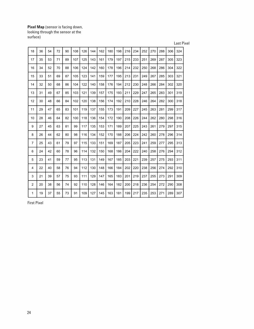
Pixel Map (sensor is facing down,looking through the sensor at thesurface)
First Pixel
Last Pixel
18 36 54 72 90 108 126 144 162 180 198 216 234 252 270 288 306 324
17 35 53 71 89 107 125 143 161 179 197 215 233 251 269 287 305 323
16 34 52 70 88 106 124 142 160 178 196 214 232 250 268 286 304 322
15 33 51 69 87 105 123 141 159 177 195 213 231 249 267 285 303 321
14 32 50 68 86 104 122 140 158 176 194 212 230 248 266 284 302 320
13 31 49 67 85 103 121 139 157 175 193 211 229 247 265 283 301 319
12 30 48 66 84 102 120 138 156 174 192 210 228 246 264 282 300 318
11 29 47 65 83 101 119 137 155 173 191 209 227 245 263 281 299 317
10 28 46 64 82 100 118 136 154 172 190 208 226 244 262 280 298 316
9 27 45 63 81 99 117 135 153 171 189 207 225 243 261 279 297 315
8 26 44 62 80 98 116 134 152 170 188 206 224 242 260 278 296 314
7 25 43 61 79 97 115 133 151 169 187 205 223 241 259 277 295 313
6 24 42 60 78 96 114 132 150 168 186 204 222 240 258 276 294 312
5 23 41 59 77 95 113 131 149 167 185 203 221 239 257 275 293 311
4 22 40 58 76 94 112 130 148 166 184 202 220 238 256 274 292 310
3 21 39 57 75 93 111 129 147 165 183 201 219 237 255 273 291 309
2 20 38 56 74 92 110 128 146 164 182 200 218 236 254 272 290 308
1 19 37 55 73 91 109 127 145 163 181 199 217 235 253 271 289 307

25
Pixel Dump PicturesThe following images are theoutput of the Pixel Data com-mand. The data ranges from 0 forcomplete black, to 63 for com-plete white. An internal AGCcircuit adjusts the shutter valueto keep the brightest feature(max pixel) in the mid 50’s.
(a) White Paper (b) Manila Folder
(c) Burl Formica (d) USAF Test Chart

26
Note:This graph is obtained by getting multiplereadings over different heights.
Shutter_Upper Address: 0x09Access: Read Reset Value: 0x01
Bit 7 6 5 4 3 2 1 0
Field S15 S14 S13 S12 S11 S10 S9 S8
Shutter_Lower Address: 0x0AAccess: Read Reset Value: 0x00
Bit 7 6 5 4 3 2 1 0
Field S7 S6 S5 S4 S3 S2 S1 S0
Data Type: Sixteen bit word.
USAGE: Units are clock cycles; default value is 0x0100HEX
. Read Shutter_Upper first, then Shutter_Lower. They should be read consecutively. Thesensor adjusts the shutter to keep the average and maximum pixel values within normal operating ranges. The shutter value may vary withevery frame. Each time the shutter changes, it changes by ±1/16 of the current value.
1.50
1.25
1.00
0.75
0.50
0.25
0
NO
RM
ALI
ZED
SH
UTT
ER V
ALU
E (C
ount
s)
DISTANCE FROM NOMINAL FOCUS (mm)
Figure 33. Typical Mean Shutter vs. z (white paper).
-1.0 -0.6 -0.2 0.2 0.6 1.0
σ
σ
3
3
–
+
XXX

The maximum value of theshutter is dependent upon theclock frequency. The formula for
For a clock frequency of 24 MHz,the following table shows themaximum shutter value. 1 clockcycle is 41.67 nsec.
Frames/second Max Shutter ShutterDecimal Hex Upper Lower
1512 12397 0x30EC 30 EC Default Max Shutter
the maximum shutter value is:
clock freqMax shutter value = – 3476 1500
Ordering InformationSpecify part number as follows:
ADNS-2610 = 8-pin staggered dual inline package (DIP), 40 per tube.
www.agilent.com/semiconductorsFor product information and a complete list ofdistributors, please go to our web site.
For technical assistance call:
Americas/Canada: +1 (800) 235-0312 or(408) 654-8675
Europe: +49 (0) 6441 92460
China: 10800 650 0017
Hong Kong: (+65) 6271 2451
India, Australia, New Zealand: (+65) 6271 2394
Japan: (+81 3) 3335-8152(Domestic/International), or0120-61-1280(Domestic Only)
Korea: (+65) 6271 2194
Malaysia, Singapore: (+65) 6271 2054
Taiwan: (+65) 6271 2654
Data subject to change.Copyright © 2002 Agilent Technologies, Inc.Obsoletes 5988-7320ENMarch 10, 20035988-9164EN
Inverse_Product Address: 0x11Access: Read Reset Value: 0xFF
Bit 7 6 5 4 3 2 1 0
Field Reserved Reserved Reserved Reserved IP3 IP2 IP1 IP0
Data Type: 4 bit number.
USAGE: Status information and type of mouse sensor
Field name Description
Reserved Reserved for future use
IP3-IP
0Inverse Product ID (x1111b or xFh)