Embed Size (px)
Citation preview
International Journal of Scientific & Engineering Research Volume 9, Issue 1, January-2018 1237 ISSN 2229-5518
IJSER © 2018 http://www.ijser.org
Power Dissipation Control Modern Trends and Techniques
Agbaje Michael*(corresponding author) Igwe Nkechi*, Ayodele Abiola*
*Babcock University
Abstract
Current technological advances clearly puts an enormous weight on battery of any cell phone. The CMOS has been the main innovation in this day and age of portable communication because of its low power utilization. Diminishment of leakage control in CMOS has been the exploration enthusiasm for the most recent few years. In CMOS incorporated circuit configuration there is an essential exchange off between innovation scaling and static power utilization. In the present CMOS innovation the leakage control utilization assumes a critical part. As we drawing closer to nano-scale plan the aggregate chip control utilization ends up plainly reliant on leakage control. Expanding the battery life in versatile wireless communication and portable processing and comparative different applications is the subject of research today. Further, since the leakage of battery exists notwithstanding when gadgets are out of gear state influences leakage to control misfortune most basic in CMOS VLSI circuits. Numerous procedures have been advanced to handle the issue it's still in advance. This paper basically concentrates on the audit of different works done in this field till the present date. Encourage an audit of late work done on another procedure Lector Stack State Retention Technique(LSSR) is talked about in the paper.
Keywords: CMOS, Dynamic power, Logic speed, Low power, Static power
1.0 Introduction
The development of CMOS coordinated circuit is a noteworthy point of reference in the historical backdrop of current innovation for both elite and versatile applications. Power dissipation is a critical parameter in the plan of CMOS ICs (Jahil J, 2013). It requires high thought in rising innovations, for example, ultra-wideband (UWB) and radio recurrence recognizable proof (RFID) and in addition wireless sensor systems (WSN) and short or long-extend communication gadgets (Uddin, et al., 2010).
In CMOS innovation, control dissipation mostly contributed by static and dynamic power. The fundamental segments that influence control dissipation are capacitive load streams, cut off and leakage ebbs and flows (Hanchate and Ranganathan, 2014). Static power dissipation happens because of leakage streams and subthreshold ebbs and flows that contribute a little rate to the
IJSER
International Journal of Scientific & Engineering Research Volume 9, Issue 1, January-2018 1238 ISSN 2229-5518
IJSER © 2018 http://www.ijser.org
aggregate power utilization. Five primary wellsprings of leakage streams in CMOS transistors are subthreshold leakage (ISUB), entryway oxide burrowing leakage (IG), turn around inclination source/deplete intersection leakages (IREV), door incited deplete leakage (IGIDL) and door current because of hot-bearer infusion (IH) (Butzen, Rosa Jr, Chiappetta Filho, Reis, and Ribas, 2010).
Components of Power Dissipation
There are two components of power dissipation:
1. Static power dissipation: The static power segments wind up noticeably essential when the circuits are very still, i.e. at the point when there is no action in the circuits and they are altogether one sided to a particular state. The static power dissipation incorporates sub edge and turned around one-sided diode leakage streams. Because of the vital yet unsafe (in a leakage-power sense) down-scaling of limit voltages, the sub edge leakage is winding up increasingly articulated.
2. Dynamic power dissipation: Dynamic power dissipation can be additionally subdivided into three instruments: switched, short-circuit, and glitch power dissipation. Every one of them pretty much rely upon the action, timing, yield capacitance, and supply voltage of the circuit. The rehashed charging and releasing of the yield capacitance is important to transmit data in CMOS circuits. This charging and releasing foundations for the switched power dissipation. The power utilization of a CMOS advanced circuit can be represented to as
Where f is the clock recurrence, C is the normal switched Capacitance per clock cycle, Vdd is the supply voltage , I short is the short circuit current and I spill is the leakage current.
i. Short circuit power dissipation: The short-circuit vitality dissipation comes about because of an immediate way current spilling out of the power supply to the ground amid the exchanging of a static CMOS door. Short-circuit vitality constitutes 10-20% of the aggregate vitality dissipation of a static CMOS entryway (Korkmaz, 2005).
ii. Glitch power dissipation: Glitches are transitory changes in the estimation of the yield – pointless advances. They are caused due to the skew in the information signs to a door. Glitch power dissipation represents 15% – 20 % of the global power.
Power Dissipation Models/Sources
IJSER
International Journal of Scientific & Engineering Research Volume 9, Issue 1, January-2018 1239 ISSN 2229-5518
IJSER © 2018 http://www.ijser.org
The aggregate power dissipation on the chip emerges from three parts which are: interconnects, device in logic, and device in memory. Interconnects are additionally delegated flagging interconnects, and clock appropriation. Logic gadgets are likewise named combinational logic and locks. The purpose behind this qualification is that clock interconnects and locks have higher
obligation cycle. For the logic and memory, power can additionally be named being dynamic or static (leakage) power. The displaying of leakage power would be indistinguishable for logic and memory. We disregard the short-circuit power in our examination, as it constitutes a little part of dynamic power.
lnterconnect power dissipation
Among flagging interconnects, just the interconnects that are a piece of the logic are demonstrated. Memory power can't be demonstrated utilizing the stochastic wire length disseminations and is considered independently. Neighborhood, middle of the road (semi-global) and global levels should be considered independently for power counts. This is on the grounds that global wires keep running at a lower clock recurrence (global clock) than the nearby and semi-global wire clock recurrence (neighborhood clock). Moreover, to limit delay, global lines utilize repeaters that are additionally considered. We utilize the stochastic wirelength dispersion created in with a Rent's example of 0.55. The most extreme length of the wire in the neighborhood level is acquired by designating it 25% of the nearby clock cycle. The division between semi-global and global wiring levels is gotten by utilizing the idea of isochronous districts, which are clock domains reachable by the semi-global wires inside a solitary nearby clock cycle. The isochronous areas are in tum associated by global wires, running at the global clock recurrence. For global lines, in light of articulations for ideal measuring and dispersing of repeaters, its capacitance is additionally ascertained and added to the global wire capacitance. Exchanging action is thought to be 0.15 for the global and semi-global interconnects, and 0.1 for nearby interconnects, where the changing action has a tendency to be lower.
B. Logic power dissipation demonstrate
The dynamic power in logic is demonstrated as the leakage power in logic will be displayed in a later sec. The dynamic power in logic is displayed as
Here, Nlogic is the quantity of transistors in logic, Wavg is the normal transistor estimate at the contribution of the entryway, and Ctrans is the door capacitance per unit length for the transistor. fld is the normal logic profundity, taken to be 12. It comes into account on the grounds that locks are dealt with independently. The width to length proportion of a normal transistor is taken to be
IJSER

International Journal of Scientific & Engineering Research Volume 9, Issue 1, January-2018 1240 ISSN 2229-5518
IJSER © 2018 http://www.ijser.org
15 and Wavg is computed in like manner. Ctrans remains around steady at 1.75fFlp. Exchanging action for logic is the same with local interconnects.
C. Memory power dissipation
The dynamic power dissipation in memory happens just amid peruses and composes. The predominant piece of the power dissipation is the charging and releasing of the immense capacitance of the bitlbit_ wires and the transistors associated with these wires. The power scattered in the decoder and the sense-speaker is little, and is dismissed here. Articulation for the exchanging of bit/bit wires is inferred in and is adjusted for our motivations to give the accompanying vitality per operation:
The above articulation expect a square design for memory, and Nmem is the aggregate number of transistors in the memory. lcol is the segment tallness, which is the square foundation of memory zone for this situation. Memory range is figured from format conderatiotis, expecting around 600X2 for every memory cell. Cdiff is the dissemination capacitance of one memory transistor (Guuruv Chandru, 2014).
Source of Dissipation in CMOS and Control Techniques
Dynamic power dissipation is the power consumed by CMOS, coming about because of short circuits current. The most huge wellspring of dynamic power utilization is the exchanging exercises of the charging and releasing burden capacitances when the yield changes amongst high and low logics (Kabbani, 2010). Since, there is an at the same time limited ascent and fall time for PMOS and NMOS, both of the transistors will be ON for a little timeframe. Coordinate current spill out of VDD to ground makes a short circuit current. In one full cycle of CMOS logic, the present streams from the VDD to stack capacitance for charging and then connected to the ground amid released. In this way, in a total cycle of charging and releasing, a sum of Q = CL.VDD is expelled from the VDD to the ground. The execution of dynamic power utilization can be enhanced by assessing Eq. (1).
P= α cv2 f -----------------------------------------------(1)
where, P is the power devoured, α the action factor, C the switched capacitance, V the supply
voltage and f the clock recurrence. A clock in a framework has action factor of α = 1, since it
rises and falls each cycle. Generally the action factor of the information is 0.5. Dynamic power
dissipation can be processed viably if the correct load capacitance evaluated at the hubs and by
IJSER
International Journal of Scientific & Engineering Research Volume 9, Issue 1, January-2018 1241 ISSN 2229-5518
IJSER © 2018 http://www.ijser.org
calculating in the movement factors. It is critical for originators and analysts to take static and
dynamic power dissipations into thought in planning low-power advanced gadgets.
Hypothetically, dynamic logic has less power disseminated contrasted with static logic because
of the nonattendance of yield glitch and capacitance diminishment (Klab, Napieralski, and De
Mey, 2010). This can be found that dynamic CMOS logics are more useful than static CMOS
logic. By the by, the precharging operations that deliver additional power dissipation don't
impact the static CMOS logic. However the quick changes in process innovation cause the
leakage power dissipation (static power) to build substantially quicker than dynamic power and
discovered prevailing over the time. Power dissipation per charge or release can be
communicated by Eqs. (2) and (3).
--------------------------- (2)
where, VDD is the power supply voltage and
……………………….(3)
given that I CG the door capacitance of ith fan-out and Cwire the capacitance of the determined
associations. Conditions (2) and (3) demonstrate the relationship of aggregate capacitance and
supply power affecting the power dissipation. Toward the starting, the power dissipation in
CMOS gadgets isn't a worry in chip plan. The emphasis is more on framework speed and
unwavering quality. In any case, in profound submicron innovation, all expended power
ordinarily disseminated as warmth and the cost of giving power has caused extraordinary
enthusiasm for power diminishment.
VLSI planners must keep the adjust in power dissipation and the circuit's execution with scaling
of the gadgets. Scaling strategies pay a noteworthy part in decreasing the power dissipation
IJSER

International Journal of Scientific & Engineering Research Volume 9, Issue 1, January-2018 1242 ISSN 2229-5518
IJSER © 2018 http://www.ijser.org
starting with one innovation hub then onto the next hub. There are different scaling strategies
utilized for VLSI circuits. Customarily, most basic are voltage scaling, stack scaling, innovation
scaling and transistor estimating (width scaling). In voltage scaling for example, supply voltage
assumes an imperative part to control the power utilization and henceforth decreasing the power
dissipation. Additionally, limit voltage of the gadget must be lessened relatively as supply
voltage decreases to maintain the transistor's yield execution. The lessening in limit voltage
expands the leakage current definitely with each new innovation age. The motivation behind
concentrate different scaling strategies is to give learning to scaling while at the same time
remembering power dissipation and proliferation delay. There are strategies to limit power
dissipations and the conceivable control procedure in CMOS logic as talked about in the
accompanying segment.
Dynamic and static power simultaneous reduction by using mapping technique
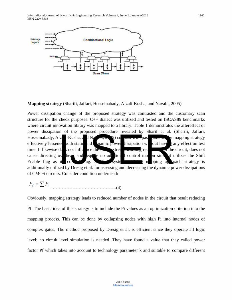
Scan-based test is one of the picked methods to take care of power issue. This technique has turned out to be well known plan for-test (DFT) strategy which gives low effect on the region and in the meantime keeping up the circuit execution. A mapping method was proposed by Sharif et al. (Sharifi, Jaffari, Hosseinabady, Afzali-Kusha, and Navabi, 2005) to obstruct the scan chain advances in part without influencing the circuit execution amid ordinary operation as portrays in the figure beneath. Power dissipation stifled the scan bind advances close to the scan cell yield by utilizing multiplexers to hinder the scan chain changes. It permitted wanted esteems while scanning the vectors in the chain. Besides, as the overwhelming segment of aggregate power dissipation, static power dissipation can likewise decrease based on an information vector control procedure joined with a technique which reorders door inputs. The example of info vector can be connected to the circuit through the arrangement of controlled contributions amid the scan mode. This work demonstrated that it essentially lessened power dissipation amid scan operations.
IJSER
International Journal of Scientific & Engineering Research Volume 9, Issue 1, January-2018 1243 ISSN 2229-5518
IJSER © 2018 http://www.ijser.org
Mapping strategy (Sharifi, Jaffari, Hosseinabady, Afzali-Kusha, and Navabi, 2005)
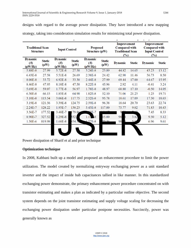
Power dissipation change of the proposed strategy was contrasted and the customary scan structure for the check purposes. C++ dialect was utilized and tested on ISCAS89 benchmarks where circuit innovation library was mapped to a library. Table 1 demonstrates the aftereffect of power dissipation of the proposed procedure revealed by Sharif et al. (Sharifi, Jaffari, Hosseinabady, Afzali-Kusha, and Navabi, 2005) contrast with past system. The mapping strategy effectively lessened both static and dynamic power dissipation without having any effect on test time. It likewise does not influence the most extreme working recurrence of the circuit, does not cause directing overhead and require no additional control motion since it utilizes the Shift Enable flag as its control flag. Another system utilizing mapping approach strategy is additionally utilized by Dresig et al. for assessing and decreasing the dynamic power dissipations of CMOS circuits. Consider condition underneath
…………………………………….(4)
Obviously, mapping strategy leads to reduced number of nodes in the circuit that result reducing
Pf. The basic idea of this strategy is to include the Pi values as an optimization criterion into the
mapping process. This can be done by collapsing nodes with high Pi into internal nodes of
complex gates. The method proposed by Dresig et al. is efficient since they operate all logic
level; no circuit level simulation is needed. They have found a value that they called power
factor Pf which takes into account to technology parameter k and suitable to compare different
IJSER
International Journal of Scientific & Engineering Research Volume 9, Issue 1, January-2018 1244 ISSN 2229-5518
IJSER © 2018 http://www.ijser.org
designs with regard to the average power dissipation. They have introduced a new mapping
strategy, taking into consideration simulation results for minimizing total power dissipation.
Power dissipation of Sharif et al and prior technique
Optimization technique
In 2008, Kabbani built up a model and proposed an enhancement procedure to limit the power
utilization. The model created by normalizing entryway exchanging power as a unit standard
inverter and the impact of inside hub capacitances tallied in like manner. In this standardized
exchanging power demonstrate, the primary enhancement power procedure concentrated on with
transistor estimating and makes a plan as indicated by a particular outline objective. The second
system depends on the joint transistor estimating and supply voltage scaling for decreasing the
exchanging power dissipation under particular postpone necessities. Succinctly, power was
generally known as
IJSER
International Journal of Scientific & Engineering Research Volume 9, Issue 1, January-2018 1245 ISSN 2229-5518
IJSER © 2018 http://www.ijser.org
………………(5)
where fclk is the clock frequency and Cout is the output capacitance. Kabbani proposed expression
is given by Eq. (6)
……………………….. (6)
where αnm is the normalized activity factor and is given as αnm = αg⁄αv, g is the gate logical
effort with given g= Ctg ⁄ Csv and p is the parasitic power dissipation where p is given by p=Ctp ⁄
Csv. The performance of the developed model in has been tested in BSIM3v3 and UMC 0.13 μm
technology by comparing modelling results with the simulation result produced by Specters.
Multi-threshold CMOS (MTCMOS) technique
MTCMOS used transistors with different limit voltages (Vt) to uptimize delay or power. Lower
voltage gadgets were utilized on basic postpone ways to limit clock periods. Higher voltage
gadgets were utilized on non-basic ways to diminish static leakage power immediately
punishment. A typical MTCMOS way to deal with decrease power is the use of rest transistors.
MOS current mode logic has been actualized in MTCMOS innovation (Anis and Elmasry, 2002).
For a considerable length of time, MTCMOS innovation was utilized to lessen leakage in
standby mode and achieved fast in dynamic mode as appeared in figure underneath. The
decrease of the working supply voltage and level shifters disposals were utilized as demonstrated
as follows. A fast 1:8 2.5 GbiVs demultiplexer was utilized as a test vehicle and 37% power
sparing was accomplished.
Besides, the MTCMOS configuration demonstrated no effect over circuit parameters, for
example, yield impedance, pick up, limit voltage vacillations and recurrence reaction.
IJSER
International Journal of Scientific & Engineering Research Volume 9, Issue 1, January-2018 1246 ISSN 2229-5518
IJSER © 2018 http://www.ijser.org
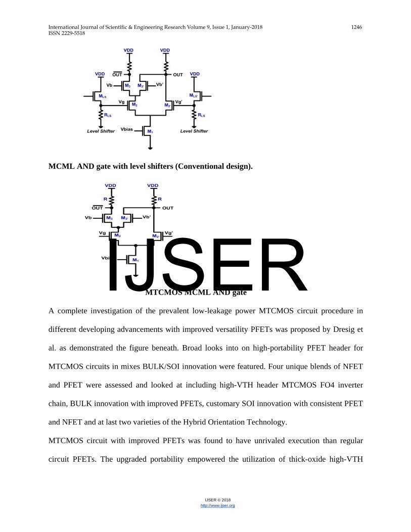
MCML AND gate with level shifters (Conventional design).
MTCMOS MCML AND gate
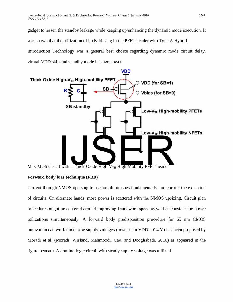
A complete investigation of the prevalent low-leakage power MTCMOS circuit procedure in
different developing advancements with improved versatility PFETs was proposed by Dresig et
al. as demonstrated the figure beneath. Broad looks into on high-portability PFET header for
MTCMOS circuits in mixes BULK/SOI innovation were featured. Four unique blends of NFET
and PFET were assessed and looked at including high-VTH header MTCMOS FO4 inverter
chain, BULK innovation with improved PFETs, customary SOI innovation with consistent PFET
and NFET and at last two varieties of the Hybrid Orientation Technology.
MTCMOS circuit with improved PFETs was found to have unrivaled execution than regular
circuit PFETs. The upgraded portability empowered the utilization of thick-oxide high-VTH
IJSER
International Journal of Scientific & Engineering Research Volume 9, Issue 1, January-2018 1247 ISSN 2229-5518
IJSER © 2018 http://www.ijser.org
gadget to lessen the standby leakage while keeping up/enhancing the dynamic mode execution. It
was shown that the utilization of body-biasing in the PFET header with Type A Hybrid
Introduction Technology was a general best choice regarding dynamic mode circuit delay,
virtual-VDD skip and standby mode leakage power.
MTCMOS circuit with a Thick-Oxide High-VTH High-Mobility PFET header
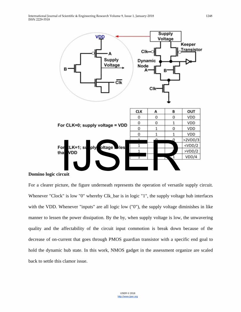
Forward body bias technique (FBB)
Current through NMOS upsizing transistors diminishes fundamentally and corrupt the execution
of circuits. On alternate hands, more power is scattered with the NMOS upsizing. Circuit plan
procedures ought be centered around improving framework speed as well as consider the power
utilizations simultaneously. A forward body predisposition procedure for 65 nm CMOS
innovation can work under low supply voltages (lower than VDD = 0.4 V) has been proposed by
Moradi et al. (Moradi, Wisland, Mahmoodi, Cao, and Dooghabadi, 2010) as appeared in the
figure beneath. A domino logic circuit with steady supply voltage was utilized.
IJSER
International Journal of Scientific & Engineering Research Volume 9, Issue 1, January-2018 1248 ISSN 2229-5518
IJSER © 2018 http://www.ijser.org
Domino logic circuit
For a clearer picture, the figure underneath represents the operation of versatile supply circuit.
Whenever "Clock" is low "0" whereby Clk_bar is in logic "1", the supply voltage hub interfaces
with the VDD. Whenever "inputs" are all logic low ("0"), the supply voltage diminishes in like
manner to lessen the power dissipation. By the by, when supply voltage is low, the unwavering
quality and the affectability of the circuit input commotion is break down because of the
decrease of on-current that goes through PMOS guardian transistor with a specific end goal to
hold the dynamic hub state. In this work, NMOS gadget in the assessment organize are scaled
back to settle this clamor issue.
IJSER
International Journal of Scientific & Engineering Research Volume 9, Issue 1, January-2018 1249 ISSN 2229-5518
IJSER © 2018 http://www.ijser.org
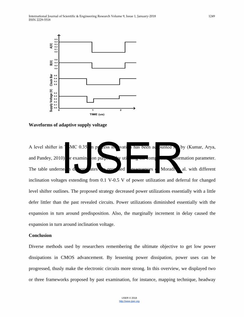
Waveforms of adaptive supply voltage
A level shifter in TSMC 0.35μm process innovation has been accounted for by (Kumar, Arya,
and Pandey, 2010) for examination purposes by utilizing the comparative information parameter.
The table underneath demonstrates the proposed consequences of Moradi et al. with different
inclination voltages extending from 0.1 V-0.5 V of power utilization and deferral for changed
level shifter outlines. The proposed strategy decreased power utilizations essentially with a little
defer littler than the past revealed circuits. Power utilizations diminished essentially with the
expansion in turn around predisposition. Also, the marginally increment in delay caused the
expansion in turn around inclination voltage.
Conclusion
Diverse methods used by researchers remembering the ultimate objective to get low power
dissipations in CMOS advancement. By lessening power dissipation, power uses can be
progressed, thusly make the electronic circuits more strong. In this overview, we displayed two
or three frameworks proposed by past examination, for instance, mapping technique, headway
IJSER
International Journal of Scientific & Engineering Research Volume 9, Issue 1, January-2018 1250 ISSN 2229-5518
IJSER © 2018 http://www.ijser.org
technique, MTCMOS methodology, forward body predisposition (FBB) technique, creamer
framework and branch target pad (BTB) procedure and adequately lessened the power
dissipation. This study fills its need to give starting rule to analysts.
References Anis, M., & and Elmasry, M. (2002). Power reduction via an MTCMOS implementation of MOS
current mode logic.
Butzen, P., Rosa Jr, L., Chiappetta Filho, E., Reis, A., & and Ribas, R. (2010). Standby power consumption estimation by interacting leakage current mechanisms in nanoscaled CMOS digital circuits.
Guuruv Chandru, P. K. (2014). SCALING TRENDS FOR THE ON CHIP POWER DISSIPATION.
Hanchate, N., & and Ranganathan, N. (2014). A new technique for leakage reduction in CMOS circuits using self-controlled stacked transistors.
Jahil J, B. I. (2013). CMOS differential ring oscillators: review of the performance of CMOS ROs in communication systems. IEEE Microwave Magazine, 14(5), 97-109.
Kabbani, A. (2010). Logical effort based dynamic power estimation and optimisation of static CMOS circuits.
Kahn, R., & and Weiss, S. (2010). Reducing leakage power with BTB access prediction.
Klab, S., Napieralski, A., & and De Mey, G. (2010). Logi-thermal simulation of digital CMOS ICs with emphasis on dynamic power dissipation.
Korkmaz, P. (2005). Modeling the Short-circuit Energy Dissipation of a CMOS Inverter.
Kumar, M., Arya, S., & and Pandey, S. (2010). Level shifter for low power applications with body bias technique.
Moradi, F., Wisland, D., Mahmoodi, H., Cao, T., & and Dooghabadi, M. (2010). Adaptive supply voltage circuit using body bias technique.
Sharifi, S., Jaffari, J., Hosseinabady, M., Afzali-Kusha, A., & and Navabi, Z. (2005). Simultaneous reduction of dynamic and static power in scan structures.
Uddin, J., Reaz, M., Hasan, M., Nordin, N., Ibrahimy, M., & M.A.M, a. A. (2010). UHF RFID antenna architectures and applications. Scientific Research and Essays, 5(10), 1033-1051.
Wang, J., Gong, N., Hou, L., Peng, X., Geng, S., & and Wu, W. (2011). Low power and high performance dynamic CMOS XOR/XNOR gate design.
IJSER

International Journal of Scientific & Engineering Research Volume 9, Issue 1, January-2018 1251 ISSN 2229-5518
IJSER © 2018 http://www.ijser.org
IJSER