Embed Size (px)
Citation preview
1
Kaushik RoyKaushik Roy
Advanced VLSI Design(ECE 695KR)
Kaushik RoyProfessor of ECEPurdue University

2
Kaushik RoyKaushik Roy
Outline
Transistors – channel having few energy statesEnergy band diagramCurrent flow & I-V CharacteristicsSubthreshold LeakageGeneralization to larger transistors
Acknowledgement: Professor Supriyo Datta

3
Kaushik RoyKaushik Roy
Attributes of a good switchGood gate control on channel Less control of drain on channelHigh ON current, less OFF current
Insulator
V“Gate”
Q
Field Effect Transistor
Channel
Source
R
Drain
R (V)
Transistors
f(E) =1/(e(E-EF)/kT+1)
EF
E
0 f01/2 1
How to understand I-V characteristicsBand diagram
-3eV
-5eV
-9eV
0eV
0eV
CB
VB
Distribution of electrons over a range of allowed energy levels:

4
Kaushik RoyKaushik Roy
VacuumLevel
ElectrochemicalPotential
µ
S Channel D
VG > 0
VG < 0
No states
FILL
EDEM
PTY
S Channel DInsulator
VG “Gate”
Gate Bias

5
Kaushik RoyKaushik Roy
Peak occurs where EF crosses an energy level due to an applied VG bias
Simple Energy Level Scenario
0 eV
E5
E4
EF
E3
E2
E1
E1 E2 E3 E4 E5
VG
IDSmall fixed VD

6
Kaushik RoyKaushik Roy
Transistors: Key Concepts
Key concepts: VD, VG, empty and full energy levels, VT, EFFermi function is centered at Ø
f0(E) =1/(eE/kT+1)
To get it centered at EF, shift itf0(E-EF) =1/(e(E-EF)/kT+1)
I
V
ChannelDrain
L
Source
EF
E
0 f01/2 1
Ev
Ec
Vaccum level
7
Kaushik RoyKaushik Roy
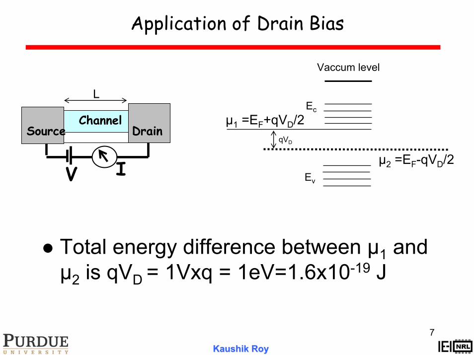
Application of Drain Bias
Total energy difference between μ1 and μ2 is qVD = 1Vxq = 1eV=1.6x10⁻¹⁹ J
IV
ChannelDrain
L
Source
Ev
Ec
Vaccum level
μ2 =EF-qVD/2
μ1 =EF+qVD/2qVD

8
Kaushik RoyKaushik Roy
Current Flow
N1: Avg. # of electrons that the left contact would like to see = 2f1(є) = 2f0(є– μ1)N2: N2 = 2f2(є) = 2f0(є – μ2)
I
V
ChannelDrain
L
Source
μ2
μ1 є
I1I2
Accounts for up-spin and down-spin that is
possible at a level

9
Kaushik RoyKaushik Roy
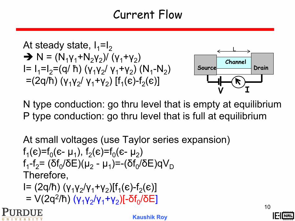
Current Flow
N: Actual # of electrons at steady state in the channel
I1: q(γ1/ћ)(N1-N)
I2: q(γ2/ћ)(N-N2)
γ/ћ : rate at which electrons cross (escape rate)ћ = h/2π=1.06x10-34 J.secγ1 and γ2 are in units of Joule
Ex: γ1=1meVγ1/ћ = 1.6x10⁻¹⁹/1.06x10-34= 10-12 /sec= 1psec for electron to escape into the channel
IV
ChannelDrain
L
Source
10
Kaushik RoyKaushik Roy
Current Flow
At steady state, I1=I2N = (N1γ1+N2γ2)/ (γ1+γ2)
I= I1=I2=(q/ ћ) (γ1γ2/ γ1+γ2) (N1-N2)=(2q/ћ) (γ1γ2/ γ1+γ2) [f1(є)-f2(є)]
N type conduction: go thru level that is empty at equilibriumP type conduction: go thru level that is full at equilibrium
At small voltages (use Taylor series expansion)f1(є)=f0(є- μ1), f2(є)=f0(є- μ2)f1-f2= (δf0/δE)(μ2 - μ1)=-(δf0/δE)qVDTherefore,I= (2q/ћ) (γ1γ2/γ1+γ2)[f1(є)-f2(є)] = V(2q2/ћ) (γ1γ2/γ1+γ2)[-δf0/δE]
I
V
ChannelDrain
L
Source

11
Kaushik RoyKaushik Roy
Current Flow
Use E = є – EF Since μ1=EF+qVD/2, μ2=EF-qVD/22q2/ћ : dimension of conductanceγ1γ2/γ1+γ2: dimension of energyδf0/δE : dimension of inverse energy
EF
E
0 f01/2 1
E 1/(4kT)
-δf0/δE

12
Kaushik RoyKaushik Roy
Current Flow
I/V = conductance = (2q2/ћ) (γ1γ2/γ1+γ2)[-δf0/δE]If f1 – f2 = 1 and γ1= γ2; I = qγ1/2ћSeems to indicate that there is no limit to conductance but
in reality, we do have a limitRmin = h/2q2 = (6.6x10⁻³⁴J-s)/2x(1.6x10-19)2 = 12.9kΩ
γ1/ћ γ2/ћStill one level
μ2
μ1
I=(q/ћ) (γ1/2)(qVD/2γ1) = q2VD/4ћOnly a fraction of levels
contribute to currentBroadening

13
Kaushik RoyKaushik Roy
Broadening
Each electronic level has a wavefunction Ψassociated with it
With no coupling, Ψ α e-iєt/ћ time domainEnergy domain (Fourier transform) we get an impulse response
Ψ2 : probability of finding the electron at a point|Ψ| is 1 for the above expression of Ψ2.
After coupling the waveform gets modifiedΨ α e-iєt/ћe-t/2ζ : lifetime associated with electron
ζ : lifetime --- the probability of finding the electron in the channelFourier transform of new Ψ gives the density of statesD(E) = (γ/2π)/((E- є)2+ (γ/2)2), γ= γ1 + γ2 = ћ/2ζ

14
Kaushik RoyKaushik Roy
Broadening
I= (q/ћ) (γ1γ2/γ1+γ2)[f1-f2]= ∫dED(E) (q/ћ) (γ1γ2/γ1+γ2)[f1-f2]
N = ∫D(E)dE(γ1f1+γ2f2/γ1+γ2)
If f1-f2=1, I= -(q/ћ) (γ1γ2/γ1+γ2)∫D(E) dE
E
є
∫D(E)dE =1
I
VD~kT
Imax=-(q/ћ) (γ1γ2/γ1+γ2)
But the channel potential gets modulated by the drain voltage!
15
Kaushik RoyKaushik Roy
Current Flow
channelμ2
μ1
E
f1(E)
E
f1(E)
1V
channel
μ2μ1
E
f1(E)
E
f1(E)
-1V
I
VD
16
Kaushik RoyKaushik Roy
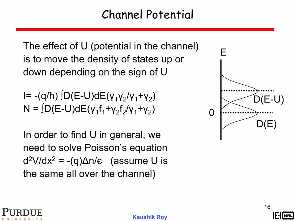
Channel Potential
The effect of U (potential in the channel)is to move the density of states up ordown depending on the sign of U
I= -(q/ћ) ∫D(E-U)dE(γ1γ2/γ1+γ2)N = ∫D(E-U)dE(γ1f1+γ2f2/γ1+γ2)
In order to find U in general, weneed to solve Poisson’s equation d2V/dx2 = -(q)Δn/є (assume U isthe same all over the channel)
0D(E)
D(E-U)
E

17
Kaushik RoyKaushik Roy
Channel Potential
Amount of charge in channel = -qΔn= CSV + CG(V-VG)+ CD(V-VD)
With VS grounded,V= (CGVG + CDVD)/(CS + CG+ CD)+ (-qΔn)/(CS + CG+ CD)U = -qV = -q(……………..) U = UL+q2/CEΔn; CE= CS + CG+ CD
Small devices, CE is small and q2/CE is large can change a lot of things
Channel VDVS
VG U: Potential energyV: Electric potential in a certain
regionU= -qV
Single electron charging energy

18
Kaushik RoyKaushik Roy
Channel Potential
IdealAs drain levels are lowered, the
DOS also wants to slide downmore available states, hence more current
UL= -q(CGVG + CDVD)/(CS + CG+ CD)Good transistors: stop DOS sliding in channel. Make UL as
large as possible (CG ) to make effect of VD negligible!
channel
μ2
μ1
E
f1(E)
E
f1(E)Source Drain
ID
VD
Small transistors of present day

19
Kaushik RoyKaushik Roy
Good Transistor
Increase CG to make the effect of VDnegligible
Gate as close as possible to the channel
If L=500A, then gate should be as close as 20A to the channel. If L is smaller, gate should be even closer, but gate leakage…
UL= -q(CGVG + CDVD)/(CS + CG+ CD)

20
Kaushik RoyKaushik Roy
Current
I= -(q/ћ) ∫D(E-U)dE(γ1γ2/γ1+γ2)(f1-f2)
N = ∫D(E-U)dE(γ1f1+γ2f2/γ1+γ2)
U = UL+U0ΔN U0 = q2/CE
CE= CS + CG+ CD
UL = [CG(-qVG) + CD(-qVD)]/CE
Need to besolved
self-consistently

21
Kaushik RoyKaushik Roy
Single Electron Charging Energy
N = ∫D(E-U)dE(γ1f1+γ2f2/γ1+γ2)U = UL+U0Δn μ2
μ1
N
μє-μ
If self consistent solution not considered
Because of term U0 in self-consistent solution, the level starts floating up as it gets filled with electrons making the
filling up process slower!
є-μ+2U0

22
Kaushik RoyKaushik Roy
Example
Sphere of charge
U=q2/4πєR= 1.6x10⁻¹⁹Coul/4x3.14x8.85x1012 F/mx10-7m ≈14meV ~ order of kT
For small devices U0 will be largerU = UL+U0(N-N0)Big devices, U0 is smaller, but (N-N0) is large
R

23
Kaushik RoyKaushik Roy
Current Flow
U0 >> kT + γ Coulomb blockage charging energy U0exceeds broadening γ.
channel
μ2
μ1
E
f1(E)
E
f1(E)Source Drain
μ1 μ2

24
Kaushik RoyKaushik Roy
Conductance (Revisited)
I= -(q/ћ) ∫D(E-U)dE(γ1γ2/γ1+γ2)(f1-f2)For small applied voltageI= -(q/ћ) D(E) (γ1γ2/γ1+γ2)qVD
Ohm’s law: G α A/L More states, more current & larger devices have more states. D α WL contradicts Ohm’s law??
γ decreases as 1/L; γ1γ2/γ1+γ2 α 1/LL cancels out!
Conductance independent of L! Ballistic device

25
Kaushik RoyKaushik Roy
xxx
Bottom-up view leads to (γ1=γ2 and U=0)I= (q γ1/ћ) ∫D(E)dE (f1(E)-f2(E))For small applied voltageUsual top down view yields an expressionI= -(S/L)nμ(μ1 - μ2)S: cross sectional area; (1/L): inverse of length; n: electron
density; μ: mobility Relate broadening to diffusion instant D, γ1=2ћD/L2
Fermi fn approximated by Boltzmann fn (“non-degenerate” assumption) f1(E)-f2(E))=e(E-μ1)/kT(μ1 - μ2)/kTD/ μ = kT/q (Einstein’s relation) and
nSL = ∫D(E)dEe(E-μ1)/kT
26
Kaushik RoyKaushik Roy
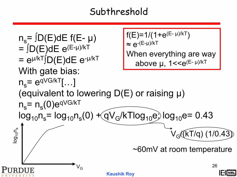
Subthreshold
ns= ∫D(E)dE f(E- μ)= ∫D(E)dE e(E-μ)/kT
= eμ/kT∫D(E)dE e-μ/kT
With gate bias:ns= eqVG/kT[…](equivalent to lowering D(E) or raising μ)ns= ns(0)eqVG/kT
log10ns= log10ns(0) + qVG/kTlog10e; log10e= 0.43
VG/(kT/q) (1/0.43)
log 1
0ns
VG
~60mV at room temperature
f(E)=1/(1+e(E- μ)/kT)≈ e-(E-μ)/kT
When everything are way above μ, 1<<e(E- μ)/kT
27
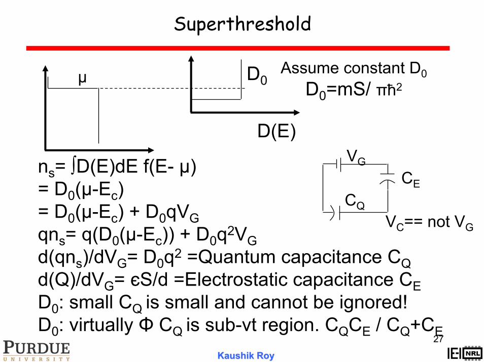
Kaushik RoyKaushik Roy
Superthreshold
ns= ∫D(E)dE f(E- μ)= D0(μ-Ec)= D0(μ-Ec) + D0qVGqns= q(D0(μ-Ec)) + D0q2VGd(qns)/dVG= D0q2 =Quantum capacitance CQd(Q)/dVG= єS/d =Electrostatic capacitance CED0: small CQ is small and cannot be ignored!D0: virtually Φ CQ is sub-vt region. CQCE / CQ+CE
D0
D(E)
μ Assume constant D0
D0=mS/ πћ2
VG
CE
CQVC== not VG