Embed Size (px)
Citation preview

United States Patent [191 Thakur et a1.
USOO5445999A
[11] Patent Number: 5,445,999 [45] Date of Patent: Aug. 29, 1995
[54] ADVANCED TECHNIQUE TO IMPROVE THE BONDING ARRANGEMENT ON SILICON SURFACES TO PROMOTE UNIFORM NITRIDATION
Randhir P. S. Thakur; Viju K. Mathews, both of Boise, Id.
Micron Technology, Inc., Boise, Id.
[75] Inventors:
[73] [21] [22] [5 1] [52]
Assignee:
Appl. No.: 975,767
Filed: Nov. 13, 1992
Int. Cl.6 .. ...................... .. H01L 21/465
US. Cl. .................................. .. 437/242; 437/246;
437/241; l48/DIG. 17 Field of Search ............. .. 437/246, 241, 242, 920;
427/61, 572; l4-8/DIG. 17
References Cited
U.S. PATENT DOCUMENTS
4,702,936 11/1987 Maeda et a1. ..................... .. 437/241
4,778,692 ll/l988 Ishihara et al. .... .. 437/241
4,949,154 8/1990 Haken ...................... .. 357/54
5,094,966 3/1992 Yamazaki et al. . .... .. 437/241
OTHER PUBLICATIONS
G. W. Yoon, et al. “Effects of Surface Pretreatment on Polysilicon Electrode Prior to Si3N4 Deposiiton” IEEE Trans. on Electron Dev. 41 (3) (Mar. 1994) pp. 347-351. N. Ajika, et a1. “Enhanced Reliability of Native Oxide Free Capacitor Dielectrics on RTN Polysilicon” Symp. VLSI Tech. Dig. (1991) (month unknown) pp. 63-64. Ito et al., “Thermal Nitridatioin of Silicon in Advanced LSI Processing”, Japanese Journal of Applied Physics, vol. 20 (1981) Supplement 20-1, pp. 33-34. Nakano et al., “A Native-Oxide-Free Process for 4mm Capacitor Dielectrics”, 1992 Symposium on VLSI Technology Digest of Technical Papers, pp. 16-17. Kaxiras, “Effect of Surface Reconstruction on Stability and Reactivity of Si Clusters”, Physical Review Let ters, vol. 64, No. 5, Jan. 1990, pp. 551-554. Rosato et al., “Ultra-High Capacitance Nitride Films Utilizing Surface Passivation on Rugged Polysilicon”, IEEE International Electron Devices, 1991, pp. 1—3.
[58]
1561
Nulman et al., “Electrical and Structural Characteris tics of Thin Nitrided Gate Oxides Prepared by Rapid Thermal Nitridation”, 1984, IEDM, pp. 169-170. Ourmazd et al., “Effect of Processing on the Structure of the 81/5102 Interface”, American Institute of Phys ics, Aug. 1988, p. 743. Joshi et al., “Performance and Reliability of Ultrathin Resistive Nitrided Oxides Fabricated by RTP”, SPIE, vol. 1393, Rapid Thermal and Related Processing Tech niques, 1990, pp. 128-129.
(List continued on next page.)
Primary Examiner-Olik Chaudhuri Assistant Examiner-C. Everhart Attorney, Agent, or Firm-Lia M. Pappas
[57] ABSTRACT The present invention teaches a method for fabricating an ultrathin uniform dielectric layer over a silicon or polysilicon semiconductor substrate. The method en tails ?rst providing a substrate having a conductive area into a chamber. Subsequently, the ?rst conductive ma terial is destabilized by introducing it to reactive gas and radiant energy in situ. The reactive gas can be Ar-Hg, H2, GeH4 or N'Fg gas. The radiant energy source can be ultraviolet (“UV”) or Tungsten Halogen lamps prefera bly having an approximate range of 0.2 to 1.6 pm to provide heat of approximately 850° to 1150" C. for approximately 10 to 60 seconds at a vacuum pressure range of lO-1o Torr to atmospheric pressure. This pro cess removes the native oxide and breaks the molecular clusters present on the silicon or polysilicon surface. Thereafter, a ?rst dielectric layer having a substantially uniform thickness forms directly above the substrate by the in situ introduction of NH3 with the radiant energy generating heat of approximately 850° to 1150° C. for approximately 10 to 60 seconds at a vacuum pressure range of 10-10 Torr to atmospheric pressure. Finally, a second silicon nitride layer is deposited by low pressure chemical vapor deposition or plasma nitridation to cre ate a combined thickness of both dielectric layers of 40 to 100 A.
18 Claims, 6 Drawing Sheets

5,445,999 Page 2
OTHER PUBLICATIONS
Rosato, Fazan, Mathews Hawthorne, Dryer, Eyolfson, Ditali, and Chan, Ultra-High Capacitance Nitride Films Utilizing Surface Passivation on Rugged Polysili con, Device Technology session to 1991 IEEE Interna tional Electron Devices Metting, pp. l-3. Nulman and Krusius, Rapid thermal nitridation of thin thermal silicon dioxide ?lms, Appl. Phys. Lett., vol. 47, No. 2, Jul. 15, 1985, pp. 148-150. J. Cable, High-Field Mobility Effects in Reoxidized Nitrided Oxide (ONO) Transistors, IEEE Transactions,
vol. 39, No. 3, Mar. 1992, pp. 607-613. Jodhi and Kwong, Influence of process parameters on the time-dependent dielectric breakdown of rapid ther mally nitrided and reoxidized thin S102, J. Appl. Phys. Lett. 60 (12) Mar. 23, 1992, pp. 1489-1491. Moslehi, Fu, Sigmon, Saraswat, Low-temperature di rect nitridation of silicon in nitorgen plasma generated by microwave discharge, J. Appl. Phys. 58(6), Sep. 15, 1985, pp. 2416-2419. K. Ando, et a1. “Ultrathin Silicon Nitride ?lms by RTP and CVD” Appl. Phys. Lett. 26 Aug. 1991 pp. 1081-1083.

US. Patent Aug. 29, 1995 Sheet 1 0f 6 5,445,999
FIG. 1a (KNOWN ART);
w , 9, , , ,
' FIG. 1b 5 (KNOWN ART)E
FIG. 10 (KNOWN ART)

US. Patent Aug. 29, 1995 Sheet 2 of 6 5,445,999
\\L\\\\\
FIG. 2c
US. Patent Aug. 29, 1995 Sheet 3 of 6 5,445,999
FIG. 5

U.S. Patent Aug. 29, 1995 Sheet 4 of 6
VOLTAGE (v) CONTROL
RTN - 1000°Cl40 SEC.
RTN - 950°C/40 SEC.
RTN - 1000°Cl20 SEC.
RTN - 900°C/6O SEC. RTP - 1000°Cl20 SEC.
RTP- 1000°Cl5 SEC.
RTP - 900°C/40 SEC.
RTP - 900°C/20 SEC.
at 1OfF/pm2
3.6 -—
3.4 —
3.2 '
3.0
6.1 5.9 5.7 5.3 5.5
CAPACITANCE (fF/pm2)
5.1
FIG. 4
US. Patent Aug. 29, 1995 Sheet 5 0f 6 5,445,999
TlME-TO-50% FAILURE (SEC)
10,000,000 '
1,000,000 —
RTP + RTN
(PROPOSED 100,000 — PROCESS)
10,000 -
1 '
RTN KNOWN AR
100 — ( T)
10
APPLIED STRESS (VOLTS)
FIG. 5
US. Patent Aug. 29, 1995 Sheet 6 of 6 5,445,999
COUNTS
25
SPUTTER TIME (MIN)
FIG. 6 (KNOWN ART)
COUNTS
SPUTTER TIME (MIN)
FIG. 7

5,445,999 1
ADVANCED TECHNIQUE TO IMPROVE THE BONDING ARRANGEMENT ON SILICON SURFACES TO PROMOTE UNIFORM
NITRIDATION
FIELD OF THE INVENTION
This invention relates to VLSI semiconductor CMOS processes and to a method for fabricating a cell capacitor over a semiconductive substrate. More partic ularly, the invention relates to a process for formulating a thin dielectric layer by promoting uniform nitridation. The invention is particularly applicable to Dynamic Random Access Memory (“DRAM”) devices.
BACKGROUND OF THE INVENTION
The continuing trend of scaling down integrated circuits has forced the semiconductor industry to con sider new techniques for fabricating precise compo nents at submicron levels. This is of particular relevance to the manufacture of DRAM devices. Dielectric layers are the foundation to the creation of cell capacitors. The expansion of the memory capacity of a DRAM device is dependent on the ability to fabricate smaller cells hav ing increased capacitances. As such, the thinner a di electric layer can be manufactured having an equivalent or increased dielectric constant, the smaller the cell.
In metal oxide semiconductor (“MOS”) technology, small, high performance transistors require thin gate and cell dielectrics. An ultrathin (élOO A) dielectric layer should minimally comprise enhanced dielectric properties. However, several additional design consid erations must be examined in the manufacture of ultra thin dielectric layers. These include uniformity in thick ness, reliability, high dielectric constant, as well as im perviousness to thermal breakdown. Ultimately, high performance, ultrathin dielectric layers should also comprise a low diffusion rate for impurities, low inter face state density, and be chemically stable. Neverthe less, the physical constraints of the materials and meth ods of fabrication employed have made the characteris tics of the dielectrics derived less than the optimum. a
Silicon dioxide, at thicknesses greater than 100 A, provides a cost effective, high quality dielectric layer for single crystal silicon or polycrystalline silicon (“polysilicon”) substrates. Nonetheless, for dielectric layers less than 100 A, silicon dioxide is known to have a high defect density and a low ef?cacy as a diffusion mask against impurity diffusion.
In light of silicon dioxide’s inherent limitations for dielectric layers of 100 A or less, several alternatives have been developed. One such alternative is the use of silicon nitride (Si3N4) as a dielectric layer. This layer can be formed on a substrate’s surface through a process which includes Rapid Thermal Nitridation (“RTN”). Under RTN, the silicon substrate is exposed to either pure ammonia (NH3) or an ammonia plasma at tempera tures approximately between 850° and l200° C. to form a silicon nitride ?lm.
Precise ultrathin dielectric layers are currently fabri cated employing RTN. However, the dielectric layers formed thereby have had several shortcomings. These ultrathin dielectrics have lacked uniformity in their overall composition. Further, they have had question able reliability in part because of their susceptibility to thermal breakdown. Hence, the overall cell capacitance of the known art is limited.
15
25
35
45
50
55
65
2 For example, in US. Pat. No. 4,949,154, inventor
Haken teaches a method of depositing a thin dielectric over a polysilicon substrate. Applying the technique of Haken, a silicon nitride layer is formed over a silicon dioxide layer, which is positioned over the polysilicon substrate. Subsequently, transistors are formed in the cleared areas of the polysilicon substrate, and a second layer of ?eld oxide is grown. This approach creates O-N-O thin dielectric layers atop the polysilicon sub strate. It is this additional oxide layer which reduces the uniformity and reliability of the overall dielectric layer.
SUMMARY OF THE INVENTION
The primary object of the present invention is to eliminate the aforementioned drawbacks of the prior art. Another object of the present invention is to pro vide a method of fabricating an ultrathin dielectric layer over a rugged and/or smooth, polysilicon or silicon substrate that has improved uniformity. A further ob ject of the present invention is to provide a method of fabricating an ultrathin dielectric layer having an in creased capacitance. Still another object of the present invention is to provide a method of fabricating an ultra thin dielectric layer having an increased time dependent dielectric breakdown and improved reliability. It is a further object of the present invention to provide a method of fabricating an ultrathin dielectric layer hav ing an increased dielectric constant.
In order to achieve these hereinabove objects, as well as others which will become apparent hereafter, a method for fabricating semiconductor wafers is dis closed wherein a rugged and/or smooth, silicon or polysilicon substrate having a ?rst conductive material is ?rst provided into a chamber. Subsequently, the ?rst conductive material is destabilized by introducing it to reactive gas and radiant energy in situ. The reactive gas can be Ar-HZ, H2, GeH4 or NF; gas. The radiant energy source can be ultraviolet (“UV”) or Tungsten Halogen lamps preferably having an approximate range of 0.2 to 1.6 pm to provide heat of approximately 850° to 1150° C. for approximately 10 to 60 seconds at a vacuum pressure range of 10'10 Torr to atmospheric pressure. Thereafter, a ?rst dielectric layer having a substantially uniform thickness forms directly above the substrate by the in situ introduction of NH3 with the radiant energy generating heat of approximately 850° to 1150° C. for approximately 10 to 60 seconds at a vacuum pressure range of 10-10 Torr to atmospheric pressure. Finally, a second silicon nitride layer is deposited in situ by low pressure chemical vapor deposition or plasma nitrida tion to create a combined thickness of both dielectric layers of 40 to 100 A.
BRIEF DESCRIPTION OF THE DRAWINGS
The present invention will be better understood from reading the following description of non-limitative em bodiments, with reference to the attached drawings, wherein below: FIGS. 1(a)-1(c) is a cross-sectional view of a silicon
substrate undergoing the steps of the known art for fabricating a thin nitride dielectric layer; FIGS. 2(a)—2(c) is a cross-sectional view of a silicon
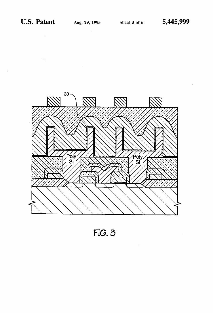
substrate undergoing the steps of the proposed process for fabricating a thin nitride dielectric layer; FIG. 3 is a cross-sectional view of the cell capacitor
structure of a DRAM device;

5,445,999 3
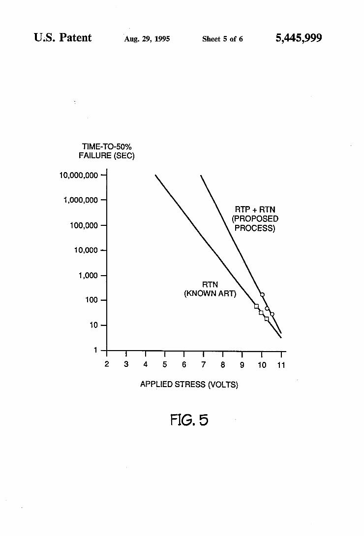
FIG. 4 is a graph depicting the effect of in situ clean ing involving Rapid Thermal Processing on dielectric characteristics; FIG. 5 is a graph comparing the Voltage versus Time
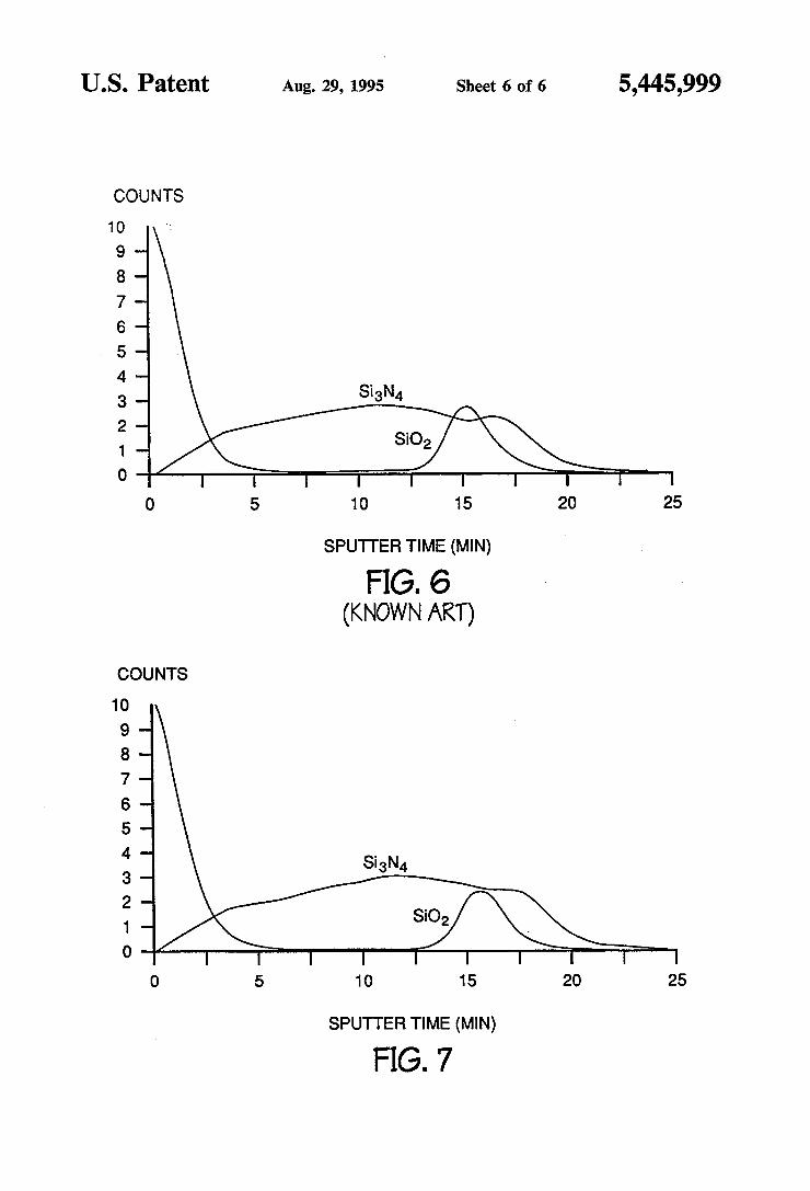
Dependent Dielectric Breakdown characteristics of the known art and the proposed process; FIG. 6 is a depth graph of a dielectric fabricated
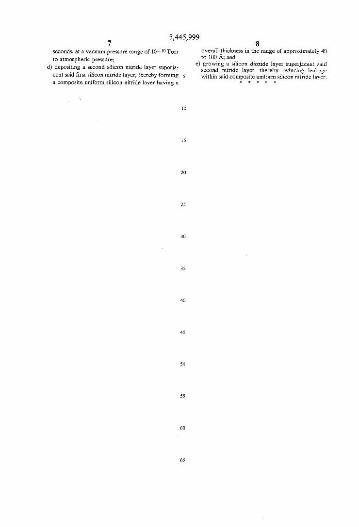
according to the known art; and FIG. 7, a depth graph of a dielectric fabricated ac
cording to proposed invention.
DETAILED DESCRIPTION OF THE INVENTION
Referring to FIGS. 1(a)—1(c), the prior art method of fabricating a dielectric layer superjacent a substrate employing the known art is illustrated. In FIG. 1(a), substrate 10, comprised of silicon or polysilicon, within a chamber is depicted. At this point in the known pro cess, substrate 10 comprises molecular clusters 14 and dangling bonds 12 on its outer surface because of its crystallized nature.
Subsequently, a native silicon oxide layer 16 forms directly on substrate 10, as shown in FIG. 1(b). The growth and con?guration of native oxide 16 directly correlates to dangling bonds 12 and silicon molecular clusters 14. The regions where silicon molecular clus ters 14 exist, a thin layer native oxide will form. In contrast, a thicker layer of native oxide will develop in regions of the substrate where dangling bonds 12 reside. This distinction is in part because molecular clusters 14 are not as reactive as dangling bonds 12.
After the native oxide 16 is formed, RTN is per formed on substrate 10 with its native oxide 16. As illustrated in FIG. 1(c), the result of this process is that a silicon nitride layer 18 develops superjacent native oxide 16. In light of the dangling bonds and silicon molecular clusters and their distinct reactivity, silicon nitride layer 18 does not comprise a uniform thickness. As a thicker layer of native oxide 16 forms over the regions of dangling bonds 12, so does silicon nitride layer 18. Thus, the resultant dielectric layer fails to reach a uniform thickness.
Referring to FIGS. 2(a)-2(c), an advanced method for improving the bonding arrangement on silicon sur faces to promote uniform nitridation is illustrated. In FIG. 2(a), step one of the invention is depicted where a substrate 20 is introduced into a chamber (not shown). Substrate 20 comprises silicon or polysilicon, and by its very nature, has a conductive path. The silicon or polysilicon can be rugged and/or smooth. Further, substrate 20 comprises dangling bonds 22 and molecular clusters 24 on its outer surface. As shown in FIG. 2(b), the second step of the inven
tion involves destabilizing the outer surface of substrate 20 to provide a uniform dangling bond configuration 26. The destabilizing process of the outer surface of sub strate 20 is accomplished by performing Rapid Thermal Processing (“RTP”) on substrate 20. RTP is a method of heating a substrate through the
use of radiation. This approach provides several advan tages over other heating techniques. First, RTP allows the surface of the substrate to reach the required pro cess temperature much quicker; in a matter of seconds. Furthermore, RTP enables the substrate’s surface to cool in a matter of seconds. In light of its quick heating and cooling characteristics, RTP protects the body of the substrate from reaching the process temperature. As such, RTP provides accurate control of the develop
25
35
45
55
4 ment of thin oxide ?lms because of the short heating / cooling time cycle. The process step of destabilizing, relying on RTP
principles, involves exposing the outer surface of sub strate 20 to reactive gas and radiant energy in situ at a vacuum pressure range of 10*10 Torr to atmospheric pressure. Ar-HZ is a preferred reactive gas because the hydrogen (H) component increases the instability of substrate 20 at lower temperatures, while the argon (Ar) component provides inert ambient characteristics. Nonetheless, H2, GeH4 or NF3 diluted with Ar-HZ can also be used. With respect to the radiant energy, a source should
preferably provide energy in the absorption band of silicon in order to properly destabilize substrate 20. In the preferred embodiment of the invention, UV lamps are employed to supply photon energy with a wave length in the approximate range 0.2 to 1.6 pm. How ever, fast heating RTP lamps, such as Tungsten Halo gen types, also can be used. As radiant energy in the presence of reactive gas is
introduced to substrate 20, the silicon molecular clus~ ters along with the already present dangling bonds are converted to form a uniform dangling bond con?gura tion 26. To this end, the radiant energy applied through this RTP step must be in the range of 850° to 1l50° C. and continue for approximately 10 to 60 seconds. As shown in FIG. 2(0), the third step of the invention
involves RTN. Applying RTN principles, the outer surface of substrate 20 is exposed to NH3 and radiant energy in situ at a vacuum pressure range of 10— 10 Torr to atmospheric pressure in situ. The source of the radi ant energy to simplify the overall process should be the same as for the process step of destabilization. The en ergy source should heat the outer surface of substrate 20 to a temperature range of approximately 850° to ll50° C. for approximately 10 to 60 seconds. In light of the reactivity of the uniform dangling bond configuration 26, a silicon nitride layer 28 having a uniform thickness forms superjacent substrate 20. The thickness of silicon nitride layer 28 ranges from approximately 15 to 40 A. To further enhance the overall dielectric properties,
an alternative embodiment of the present invention includes depositing an additional silicon nitride layer (not shown) in situ. In certain applications, such as the cell capacitance structure in DRAM device illustrated in FIG. 3, the dielectric layer 30 must have a speci?ed thickness. Thus, to enhance the overall dielectric integ rity, an additional silicon nitride layer is deposited su perjacent silicon nitride layer 28. This deposition step can be accomplished by low pressure chemical vapor deposition, as well as plasma nitridation techniques. The overall result yields a dielectric layer of silicon nitride on the order of approximately 40 to 100 A.
In another alternative embodiment, subsequent to forming a dielectric layer of silicon pitride having a thickness of approximately 40 to 100 A, a layer of sili con dioxide (not shown) can be formed in situ superja
‘ cent to further reduce leakage within the dielectric.
65
Unlike the prior art approach, the present invention presents a dielectric layer having a substantially uni form thickness comprised of silicon nitride including an silicon dioxide layer superjacent, as opposed to subja cent, to the silicon nitride layer. By applying the hereinabove invention, a cell capaci~
tor having improved dielectric characteristics can be fabricated, as shown in FIG. 4. FIG. 4 illustrates the effects of in situ cleaning involving RTP on dielectric

5,445,999 5
characteristics. The hereinabove invention also pro vides enhanced time dependent dielectric breakdown properties, as shown in FIG. 5.
Referring to FIGS. 6 and 7, a depth analysis compari son of a dielectric fabricated according to the known art with the proposed hereinabove invention is provided. In the proposed invention, the levels of silicon dioxide reach a reducedyalue of that of silicon nitride, as shown in FIG. 7. '
While the particular process as herein shown and disclosed in detail is fully capable of obtaining their objects and advantages herein before stated, it is to be understood that it is merely illustrative of the presently preferred embodiments of the invention and that no limitations are intended to the details of construction or design herein shown other than as described in the appended claims. We claim: 1. A rapid thermal nitridation (RTN) method for
fabricating uniform, thin nitride ?lms, comprising the steps of:
a) providing a silicon substrate comprising a polysili con material in a rapid thermal processing cham ber, said polysilicon material having molecular clusters and dangling bonds;
b) forming a uniform dangling bond con?guration by introducing reactive gas at a high temperature, said high temperature being in the approximate range of 850° C. and 1150’ C., said reactive gas comprises at least one of Ar-H2, H2, GeH4, and NF3 diluted with Ar-Hg; and
0) growing a ?rst substantially uniform, thin nitride layer superjacent said polysilicon material by intro ducing NH3 while rapidly heating said silicon sub strate in situ.
2. A method according to claim 1, further comprising the step of:
d) depositing a second substantially uniform, thin nitride layer superjacent said ?rst substantially uniform, thin nitride layer thereby forming a com posite nitride layer having an overall thickness.
3. A method according to claim 2, further comprising the step of:
e) positioning a second polysilicon material superja cent said second substantially uniform, thin nitride layer to form a capacitor.
4. A method according to claim 2, further comprising the step of:
e) growing a silicon dioxide layer superjacent said second substantially uniform, thin nitride layer to reduce leakage within said composite nitride layer.
5. A method according to claim 2, wherein said de positing comprises low pressure chemical vapor deposi tion.
6. A method according to claim 2, wherein said de positing comprises plasma nitridation.
7. A method according to claim 1, wherein said chamber is pressurized at a substantially low vacuum pressure.
8. A method according to claim 7, wherein said sub stantially low vacuum pressure is in the approximate range of l0—1O Torr to atmospheric pressure.
9. A method according to claim 1, wherein said high temperature is generated by radiant energy having a wavelength in the approximate range 0.2 to 1.6 pm.
10. A method according to claim 9, wherein said radiant energy comprises photon energy in the absorp tion band of silicon.
20
25
30
35
45
50
55
65
6 11. A method according to claim 1, wherein said high
temperature is generated by means of a Tungsten Halo gen lamp.
12. A method according to claim 1, wherein said high temperature is generated by means of a UV lamp.
13. A method according to claim 1, wherein said silicon substrate is in either single-crystal or polycrys talline form.
14. A method according to claim 1, wherein said radiant energy is applied for approximately 10 to 60 seconds at a vacuum pressure range of 10-10 Torr to atmospheric pressure.
15. A method according to claim 1, wherein said ?rst uniform, thin nitride layer‘ has a thickness in the approx imate range of 15 to 40 A.
16. A method according to claim 2, wherein said overall thickness of said composite nitride layer is in the approximate range of 40 to 100 A.
17. A rapid thermal processing method for fabricat ing thin ?lm dielectrics, comprising the steps of:
a) providing a substrate having a conductive material within chamber, said substrate comprising silicon material, said ?rst conductive material comprising molecular clusters and dangling bonds;
b) destabilizing said molecular clusters to form a uni form dangling bond con?guration by introducing in situ reactive gas at a temperature greater than l0OO° C. continuously for approximately 10 to 60 seconds, at a vacuum pressure in the range of 10-10 Torr to atmospheric pressure, said reactive gas comprises at least one of Ar-Hg, H2, GeH4, and NF3 diluted with Ar-H2, thereby providing said conductive material with a uniform dangling bond con?guration;
0) growing a ?rst thin dielectric layer having a thick ness of less than 30 A superjacent said conductive material by introducing in situ NH; at a tempera ture greater than l0OO° C. continuously for approx imately 10 to 60 seconds, at a vacuum pressure range of 10"10 Torr to atmospheric pressure;
(1) depositing a second thin dielectric layer dielectric superjacent said ?rst thin dielectric layer, thereby forming a composite dielectric layer having an overall thickness in the range of approximately 40 to 100 A; and
e) re-oxidizing said composite dielectric layer, thereby forming a silicon dioxide layer superjacent said second thin dielectric layer, thereby reducing leakage within said composite dielectric layer.
18. A method for fabricating thin ?lm capacitors, comprising the steps of:
a) providing a semiconductor substrate having polysilicon within chamber polysilicon comprising molecular clusters and dangling bonds;
b) precleaning said substrate by introducing in situ reactive gas and radiant energy, in the range of 850° to ll50° C.‘ continuously for approximately 10 to 60 seconds, at a vacuum pressure in the range of at least l0—l0 Torr to atmospheric pressure, said reactive gas comprises at least one of Ar-H2, H2, GeH4, and NF3 diluted with Ar-Hg, thereby pro viding said polysilicon with a uniform con?gura tron;
c) growing a ?rst silicon nitride layer having a thick ness in the range of approximately 15 to 40 A su perjacent said polysilicon by introducing in situ NH3 and radiant energy, in the range of 850° to ll50° C. continuously for approximately 10 to 60
5,445,999 7
seconds, at a vacuum pressure range of 10-10 Torr
to atmospheric pressure; d) depositing a second silicon nitride layer superja
cent said ?rst silicon nitride layer, thereby forming a composite uniform silicon nitride layer having a
5
1O
15
25
35
40
45
55
65
8 overall thickness in the range of approximately 40 to 100 A; and
e) growing a silicon dioxide layer superjacent said second nitride layer, thereby reducing leakage within said composite uniform silicon nitride layer.
* * * * *