Embed Size (px)
Citation preview

F R A U N H O F E R I N s t I t U t E F O R E l E c t R O N I c N A N O s y s t E m s E N A s
AdvAnced SyStem engineering
Design of Electrical and Multi-Physical Systems
The spectrum of tasks during the development of complex
micro and nanoelectronic systems encompasses all relevant
areas of system design, starting from the chip, through
packages and modules right up to the PCB. A major focus of
this work lies on the characterization of complex electronic
systems by modeling, simulation and measurement of para-
sitic electromagnetic effects. For this purpose the department
ASE employs several commercial simulation tools, such as CST
Studio Suite and Agilent ADS, as well as highly sophisticated
measurement instruments that allow for the analysis of a
large diversity of parasitic effects. The combination of these
disciplines allows to characterize and analyze new technolo-
gies like e.g. wireless power and data transfer, 3D molded in-
terconnect devices (3D-MID) and sensor systems even before
manufacturing prototypes.
Since with increasing levels of complexity of systems to be sim-
ulated the time costs and therefore the overall costs increase,
an efficient and precise modeling that enables significant
reductions in calculation time is needed. Thus, techniques are
analyzed in order to find the transmission behavior of very di-
verse structures that best approximate the time and frequency
domain behavior. For nonlinear systems this is achieved by
using neuronal networks. By employing specific methods
to identify parameters and systems, the input and output
behavior of complex systems can thereby be approximately
described. For the class of nonlinear systems new concepts,
methods and algorithms are being researched and developed
as well as automated design concepts (i.e. hardware / software
co-design) that are linked with commercial software products
are being created.
A further key research area, the department ASE is focused on,
is the analysis and advancement of accurate and very time and
computer resource efficient event-driven simulation models
for mixed-signal systems. An example for such a system is the
phase-locked loop (PLL). It is required in applications ranging
from modulation and demodulation, clock and data recovery
up to the synchronization and frequency synthesis. For an
optimal and robust design of PLLs an efficient model for the
highly nonlinear behavior of such circuits is essential. Hence,
non-ideal effects like e.g. dead zone, voltage controlled oscil-
lator characteristic and noise are being incorporated into an
event-driven model to optimize the design for a large range
of different boundary conditions as well as to increase overall
quality of the application.
Fig. 1: Wireless supply of consumer electronic.
Fig. 2: Near-field electromagnetic mapping on chip
level.
Fig. 3: Efficient modeling for fast simulations and
design of mixed-signal systems.
Fig. 4: Signal integrity simulation of a 3D system
for automotive application.
1
industrial custom needs. Already in the early design stages, the
constitution of these systems on both electronic and antenna
sides takes all relevant disturbances like conducted or radiated
parasitical electromagnetic effects into account. This approach
allows to guarantee the electromagnetic compatibility (EMC), the
signal integrity (SI) and the electromagnetic reliability (EMR) from
the IC-level through packages up to the printed circuit board.
Beside wireless sensing and communicating systems, the depart-
ment ASE has developed a strong know-how in the area of cordless
energy transfer with high efficiency. For this, an optimized antenna
array structure combined to a self-adaptive driving power electronics
device was designed. This smart combination of antenna and elec-
tronics increases both the efficiency and the positioning freedom
of the system by limiting drastically the produced electric smog,
making the system applicable in close proximity to human beings.
In order to conduct such research, methods for the calculation
of electromagnetic fields and circuits are applied at both analoge
and mixed-signal levels in order to analyze the transmission
behavior (i.e. crosstalk, reflection, changes of the nominal signal
waveform) in the time and frequency domain. Advanced and
precise simulation models and algorithms like the event-driven
approach enable the very fast simulation and characterization
of mixed-signal systems, reducing drastically the needed design
time and thus the time to market gap. These methods are linked
via well-defined interfaces with established software, such as
Cadence/Spectre, SPICE or Matlab/Simulink, to enable efficient
and robust top-down designs and bottom-up verifications.
The current developments of micro and nano technologies are
fascinating. Undoubted they are playing a key role in today’s prod-
uct development and technical progress. With a large variety of
different devices, different technologies and materials they enable
the integration of mechanical, electrical, optical, chemical, bio-
logical and other functions into one system on minimum space.
The Fraunhofer Institute for Electronic Nano Systems ENAS
focuses on research and development in the fields of Smart
Systems Integration by using micro and nano technologies with
partners in Germany, Europe and worldwide. Based on prospec-
tive industrial needs, Fraunhofer ENAS provides services in:
� Development, design and test of MEMS and NEMS (micro and
nano electromechanical systems)
� Wafer-level packaging of MEMS and NEMS
� Metallization und interconnect systems for micro and nano
electronics as well as 3D integration
� New sensor and system concepts with innovative material
systems
� Integration of printed functionalities into systems
� Reliability and security of micro and nano systems
The main research effort of the department Advanced System
Engineering (ASE) is focusing on designing robust micro and na-
noelectronic systems by using efficient simulation methods and
by measuring and characterizing precisely their performances.
Especially, an expertise in the area of wireless sensor systems
including Radio-Frequency and RFID technologies for harsh
environments was developed and finds its application in specific
2 3 4
I 3 2
Wireless Sensor Systems
Modern industrial systems such as conveyor and production
systems, wind turbines or aircrafts, are exposed to high loads
and an associated wearout. To avoid failures due to unforeseen
defects, a continuous sensory monitoring of such components
is crucial. In this context, the engaged sensor systems must
generate a digital and failure-free output signal that automati-
cally adapts to the input variables of event space and allows an
independent signal optimization by the fusion of different input
signals (e.g. temperature, power, speed, acceleration, etc.).
The parallel detection of several system parameters and the
combination of various sensor signals allow the detection and
compensation of defective sensors or faulty information in situ.
At the same time, the sensor data should be measured directly
on the manufactured work piece or critical moving parts (drives,
blades of wind turbines). This limits the use of classically wired
sensor systems largely. To overcome the limitations, small sen-
sors that permanently monitor their surroundings and transmit
observed data wirelessly form the core of such systems. These
sensors usually require a processor, some memory and a wire-
less sending and receiving unit for the assessment and the
transmission.
In order to allow a sensor to run autarkic it needs an integrated
energy supply. Most easily a battery can be applied. However,
for employing sensors without a time limitation and without the
need of maintenance, an energy-harvesting concept that uses
external energy from sources as sunlight, warmth, vibrations,
movement or even a wireless energy supply has to be imple-
mented. Especially in the field of energy supply of such systems
the ASE has many years of experience in the development
and deployment of intelligent RFID systems and the inductive
energy transfer under harsh industrial conditions collected in a
large number of funded and industrial projects. This knowledge
base on highly efficient modeling and analysis methods for the
characterization of high frequency electromagnetic systems,
takes hard EMC conditions among others into account. Our de-
partment is researching the realization and integration of com-
plete sensor systems that incorporate existing methodologies
and technologies from the fields of sensor technology, wireless
data and energy transmission, as well as energy harvesting.
The highest demands are made regarding complete systems
in respect to energy efficiency, flexibility and overall size. They
are also required to be multifunctional and cost-effective. In
order to be able to efficiently dimension, optimize and read a
new sensor, it is necessary to adapt or re-design the assessing
electronics, the energy supply and the transmission of data for
every individual application situation. Therefore it is the goal of
the research and development conducted by the department
ASE to provide innovative, customer-orientated solutions for
the optimization of existing methods and techniques.
Wireless Energy Supply
When considering the area of wireless communications, many
different interfaces has been established, supporting the
global strategy of Internet of Things. Recent issues of electronic
devices show a growing need of wireless energy supply for
portable devices and intelligent systems with embedded sen-
sors and actuators. The energy supply system of current mobile
equipment used in medicines (like implants), industrial produc-
tion environments or consumer electronics (like smartphones)
based on a cabled energy supply or chemical energy storage
(like batteries) has to be maintained and regularly replaced or
recharged. Thus, the most important advantage of a wireless
energy transmission system is related to the spatial positioning
freedom it offers, avoiding complicated chunky cabling and
galvanic contacts. A further advantage of a contactless energy
system is given by the possibility of encapsulating hermetically
the systems, isolating them from unwanted external impacts
(like dust, humidity, heat, etc.).
In order to supply a device wirelessly with energy, several
feasible methods exit and rely on different physical concepts.
In the case of a near-field transmission, the inductive and the
capacitive couplings are recommended. For higher ranges,
the energy transmission can take place using electromagnetic
propagating waves. By considering the classical inductive cou-
pling technology, coils and ferromagnetic materials are used in
order to guide the magnetic field from the transmitter to the re-
ceiver. Such designs operating in low frequencies typically lead
to bulky and heavy structures which restrict their integration
within surfaces or limited volumes. A space-saving integration
is achieved by using higher frequencies which allow the use
of conventional printed circuit boards for the antenna design.
At the same time, these higher frequencies offer the possibil-
ity of optimized efficiency combined with higher transmitted
energy to be transmitted. Typical point-to-point RFID-based
energy transmission systems (RFID or other systems) operate
with frequencies ranging from 70 kHz up to 30 MHz. With
such techniques, the transmittable energy is in the magnitude
of 100 mW up to 100 W with an efficiency comparable to the
charging and discharging cycle of accumulator systems.
The increase of both efficiency and positioning freedom of
wireless energy transmitting systems taking into account the
legislative electric smog limits is a top technological issue for
the market penetration of wireless transmitting systems. Only
an emission-reduced architecture can allow applications in close
proximity to human beings or in EMC critical environments. To
achieve this, the department ASE has developed an array of
juxtaposed and interlaced coils which are controlled separately.
By detecting the presence or absence of an authorized receiver,
only the transmitting coil in front of a corresponding receiver is
activated, increasing the transmission efficiency by minimizing
the radiated unwanted fields. Based on this very innovative
approach, the department ASE has built up a solid know-how
in the area of wireless energy transmission which is offered
as technological upgrade service in application domains like
medical devices, industrial automatization and consumer
electronics.
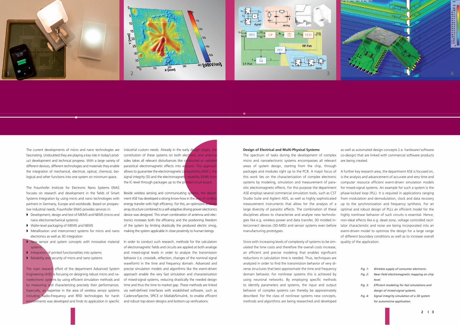
Fig. 5: RFID design for specific harsh environment applications.
Fig. 6: Far field of smart sensor module.
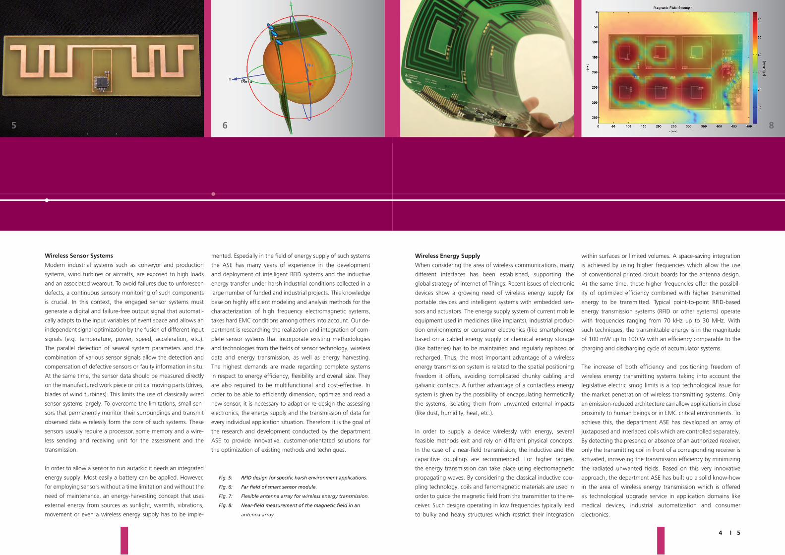
Fig. 7: Flexible antenna array for wireless energy transmission.
Fig. 8: Near-field measurement of the magnetic field in an
antenna array.
5 6 7 8
I 5 4

Electromagnetic Near-Field Measurement Techniques
The More-Moore and More-than-Moore assembly trend of smart
low-power electronic systems make the components become
continuously smaller integrating heterogeneous functionalities with
smaller switching times and therefore reduced energy consumption.
In parallel, the signal-to-noise ratio decreases, making every new
generation of a circuit more sensitive. For the developers of elec-
tronic circuits this results in increasing electromagnetic compatibility
issues. Not only the electronic device itself needs to be protected but
progressively each individual component on the printed circuit board
must be considered. These boundary conditions require a focus on
the parasitic influences during the system design to guarantee a
flawless design. By using appropriate EDA tools and simulators, it
is possible to analyze a multitude of such parameters in the design
phase. However this does not allow for sufficient security, since
the ratio between the biggest dimension (PCB) and the smallest
structure (bond wire) can differ by several orders of magnitude and
leads to extremely complex 3D models. Indeed, the radiating char-
acteristics are directly determined by the switching behavior of the
circuit and its geometric structure. Moreover, the internal signal level
and the internal signal form of integrated circuits are not known
and therefore assumptions have to be made.
Near-field measurement technique provides a mitigation to this
problem. They allow the precise detection of weak electric and
magnetic fields within a resolution of a hundredth of a millimeter
and can be employed for the characterization and discrimina-
tion of potential electromagnetic interference (EMI) sources in
active systems. This measurement technology has the ability not
only to locate EMI sources locally but also spectrally. Thanks to
this dual property, it is possible to quickly and directly identify
and correct conception faults at early design stages. However,
near-field measurement systems need to be adjusted to the spe-
cific requirements of EMC compliance measurements. For these
adjustments, the department research focuses on the influence
of the near-field probe on the field to be analyzed itself and has
developed methodologies to compensate this influence.
Such compensation is necessary, since a real probe is not only sensi-
tive to the desired field component (i.e. the normal component of
the E-field) but also on other field components such as the tangen-
tial E- and H-fields. A central research point of the department ASE
related to this issue is the continuous improvement of the mechani-
cal and electronic components of the near-field scanning system.
Beside the application field of EMC, the high and wide-band
sensitivity of the developed near-field measurement technology
allows the electromagnetic analysis of security-relevant systems
such as smart cards, which is a new and promising application
area of this advanced measurement system. By using near-field
measurement methods it is possible to uncover weaknesses in
such systems and elaborate countermeasure strategies.
Services and Measurement Techniques
The department Advanced System Engineering provides
customer-specific developments for industry and research insti-
tutes. All presented areas of research are available for services.
In the following a short survey of special services and used
measurement techniques is listed.
We offer the following services:
� Research and design of customer-specific electronic modules
� Model-based development methodologies for heteroge-
neous systems
� Development and optimization of RF antenna structures and
circuits (RFID, WLAN and others) based on simulation and
measurement methods
� Development of wired and wireless sensor systems
� EMC and EMR analysis, characterization and modeling of
micro and nano electronic circuits and of parasitic electro-
magnetic effects
� Signal integrity analyses
Equipment:
� 3D near-field scanner for DUT sizes up to 50 x 80 x 50 cm;
frequency range: DC – 6 GHz, optical contour determination
of DUT surface
� 4-port network analyzer (Agilent N5230A):
frequency range: 30 kHz – 20 GHz; application: vectorial
characterization of 4-port networks
� Impedance analyzer (Agilent 4294A): frequency range: 40 Hz –
110 MHz; application: characterization of lumped complex
components, single port networks in low frequency domain
� Spectrum analyzer (HP 8563 E): frequency range: 9 kHz –
26 GHz; application: scalar frequency domain measure-
ments, e.g. analysis of radiated spectrum of DUT
� Communication Signal Analyzer (Tektronix CSA 803):
application: Time Domain Reflectometry characterization of
transmission paths (20 GHz bandwidth), localization of imped-
ance mismatches in transmission lines (e.g. cables) with ~ 5 mm
resolution, high-speed sampling oscilloscope (up to 50 GHz)
� FCC TEM Crawford Cell (FCC-TEM-JM1):
frequency range: DC – 1200 MHz; application: immission and
emission analysis for small objects such as ICs, modules, etc.
� Waferprober Cascade Summit 9000:
application: direct RF-conform probe testing of wafers or mi-
cro systems; probes can be placed with micrometer precision
� 4-channel oszilloscope (LeCroy waveRunner 640Zi):
band width: 4 GHz, 40 GS/s; application: characterization
of high-frequency time domain signals, analysis of single
events in long-time intervals by software controlled event
triggers, synchronous analysis of analog (4 channel) and
digital (18 channel) signals.
Simulation Environment:
� CST STUDIO SUITE: Complete technology for 3D EM simula-
tion; application: analysis of electromagnetic, electrostatic,
magnetostatic and thermal behavior of 3D structures, com-
bination of 3D simulation and circuit simulation results
� ANSYS Multiphysics application: 3D simulation of electro-
magnetic, mechanical and thermal effects
Fig. 9: Advanced near-field measurement system.
Fig. 10: Near-field measurement of an RFID structure with localized EMC-
disturbance.
Fig. 11: Electronic simulation of an optimized eWLB package.
Fig. 12: Thermal analysis of a PCB assembly: simulation and measurement.
9 10 11 12
I 7 6

Contact details:
Fraunhofer Institute for Electronic Nano Systems ENAS
Department Advanced System Engineering
Warburger Strasse 100
33098 Paderborn
Germany
Head of department Advanced System Engineering:
Dr. Christian Hedayat
Phone: +49 5251 60-5630
Fax: +49 5251 60-5621
E-mail: [email protected]
Internet: http://www.enas.fraunhofer.de/EN
Front page:
Complex antenna matrix structure and electronics for wireless
energy transmission.
Photo acknowledgement: Fraunhofer ENAS