Embed Size (px)
Citation preview
Advanced Power Electronics for HVDC Applications
Michel Mermet-Guyennet
March 2015

Presentation Supergrid Institute
Applications : VSC HVDC & DCDC HVDC-MVDC
Energy efficiency : potential of SiC devices
Prospective on high voltage SiC devices
Conclusion
2
Overview

The Super GridAn electricity transmission system, mainly based on direct current, designed to facilitate large-scale sustainable power generation in
remote areas for transmission to centres of consumption, one of whose fundamental attributes will be the enhancement of the market in
electricity".
Friends of the supergrid
DC + dynamic stability management power electronics becoming key technology
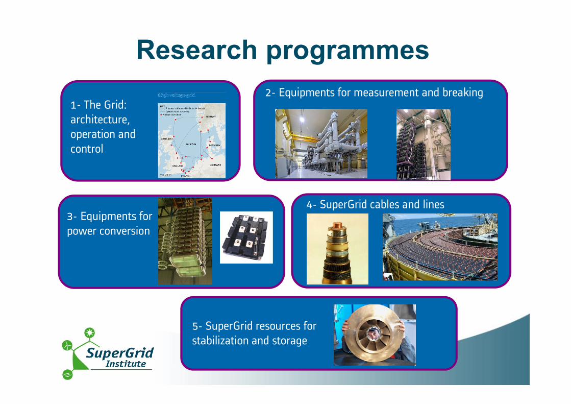
Research programmes
1- The Grid: architecture, operation and control
2- Equipments for measurement and breaking
3- Equipments for power conversion
4- SuperGrid cables and lines
5- SuperGrid resources for stabilization and storage
Presentation Supergrid Institute
Applications : VSC HVDC & DCDC HVDC-MVDC
Energy efficiency : potential of SiC devices
Prospective on high voltage SiC devices
Conclusion
5
Overview

TITRE DE LA PRESENTATION - INTERVENANT - DATE -

Off-shore wind farm connection

MaxSine® Valve Key Features
Coolant Return
Optical Fibre Routing
Coolant FlowBase Insulators
Inter-tier Insulators
Stress ShieldsIGBT1
IGBT2
R1
C1
D1
D2
T1
SW1
Sub-Module
VSC MMC

Consider a 1 GW transmission line
Consider the VSC MMC converter with 99% efficiency
Consider you sell electricity at 0,1 €/kWh
You loose 10 MW in nominal condition :
You loose 1000 € every hour in nominal condition per VSC (2000 € both ends)
You have to cool 10 MW of thermal power dissipation per converter (strong impact on acquisition cost and reliability of your VSC)
If you improve VSC efficiency by 0,1%
You gain 100€ every hour in nominal condition per VSC (200€ both ends)
You gain 438 000 € every year (based on 6 month nominal operation over one year)
You gain 876 000 € every year on both VSC converter !
9
What is at stake !

TITRE DE LA PRESENTATION - INTERVENANT - DATE -

Example of topology for DC grid collector
A
DCDC made with DAB (Dual Active Bridge) with many options (resonant, multiple-phase, modulations, ...) coupled with Medium Frequency Transformer (working in kHz range).
Typical power of DCDC is 10 MW with voltage in MVDC range and high ratio of transformation but with isolation primary-secondary in HVDC range
TITRE DE LA PRESENTATION - INTERVENANT - DATE -

lnnovative topologies and control of power converter for DC grid applications
Medium frequency transformer
High Voltage Silicon Carbide (SiC) technology and new generation of HV SiC components with packaging, gate-drive & passives
Design machine for power converter & MF transformer with virtual prototyping approach
Back to back MMC vs cascaded DCDC
ConverterTopology
Local Control
Objective FunctionsEfficiency
Link with DC GridControl
Constraint FunctionsHarmonic rejectionsExternal defaults=
lightning, short circuitFull operation time
Sub-systemPhysical Design
MFT Design
PE Design
SiCchips
PE DesignPack
PE DesignGateDrive
PE Caps or SSE
SySML
Multiphysics based design = MAXWELL3D – ANSYS3D
Mech+Therm-Q3D
Electric SimulatorSimplorer
PSIM
Control system SimulatorMATLAB-Simulink
Control Boards
EMTP-RVfor network simulation
VHDL-AMS
3D SolidCreo Essential II
Solid-Edge
Key technologies for future DC Grid

Presentation Supergrid Institute
Applications : VSC HVDC & DCDC HVDC-MVDC
Energy efficiency : potential of SiC devices
Prospective on high voltage SiC devices
Conclusion
14
Overview

Si will be widely used in BV 15V-150V
SiC will be dedicated to HV BV 1,2 kV-20kV+ and high current 100A per chip. Fact is SiC thermal conductivity is three times higher than GaN thermal conductivity
GaN will adress the range BV 600V-1200V+ and nominal current 2-30A per chip in application with high cost constraint
15
SiC vs GaN (and others)
150V
Schottky Si
Transistor MOS
JBS SiC -> PiN
Switch SiC
Schottky GaN
Switch GaN
20kV+
Volt
100
2
30
0.6-1,2kV
Diamond - AlN
>2020
Nominal
current
per chip
(A)
Breakdown Voltage

SiC : breakthrough in MMC efficiency
16
INFINEON FZ1500R33HL3IGBT 3300V 1500A
CREE MOSFET 3300V 40 mOhms
- Two cases : 30 chips in parallel and 50 chips in parallel
- No additional diodes in anti-parallel = use of reverse conducting property of MOSFET
- Same characteristics reverse/direct
- Equivalent MOSFET = 3300V 1 mOhm

Characteristics 30 chips //
17
VDS (V)
I D(A
)
Total surface area of Si = 50 cm2
Total surface area of SiC = 14 cm2
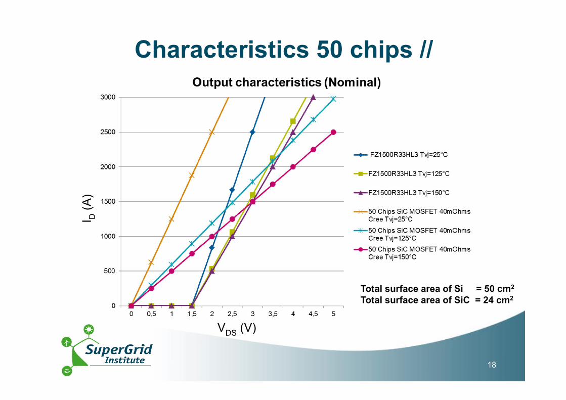
Characteristics 50 chips //
18
VDS (V)
I D(A
)
Total surface area of Si = 50 cm2
Total surface area of SiC = 24 cm2

Loss calculation
- Two approaches:- Calculation of Power Losses for MMC-based VSC HVDC
Stations - Phil S Jones & Colin C Davidson
- Comparison of High Voltage Modular AC/DC converters –P. Ladoux, P. Marino, G. Raimondo, N. Serbia
- Application case for calculation:- P = 100 MW
- Vd =+- 160 kV
- Fsw=200 Hz
- Inverter mode
- M=0,85
- Vv=2000V
- Dynamic characteristics for SiC extrapolated Eon /5 Eoff/10
19

Static and dynamic losses
20

Temperature dependance of losses
21
Presentation Supergrid Institute
Applications : VSC HVDC & DCDC HVDC-MVDC
Energy efficiency : potential of SiC devices
Prospective on high voltage SiC devices
Conclusion
22
Overview

Prospective view on HV SiC
Chips
Breakdown
Voltage
1700V 3300V 6500V 10 kV 15 kV 20 kV
Technology &
Status
MOSFET&JFET
40 mOhms
JBS 50A
MOSFET&JFET
40 mOhms
JBS 45 A
MOSFET ?
JBS ?
Bip based
PiN
Bip based
PiN
Bip based
PiN
Potential
development
chips
Available on the
market
Available on the
marketWill be available
on the market
Technology
development
Design and make
prototypes
Technology
develoment
Technology
development
Potential
development
multi-chips &
pack
-Paralleling for
low on state
-Fs to 40 kHz
-Reverse
conducting
-Paralleling for
low on state
-Fs to 40 kHz
-Reverse
conducting
-Auto supply
-Fail to short
Same as 3,3 kV -Paralleling for
low on state
-Fs to 30 kHz
-Auto supply
-Series
association of 3,3
kV
-Fail to short
Same as 10 kV Same as 10 kV
Product
objective
1500A -
1mOhm
250 A
2500A

24
10 kV Diodes
8 kV
10 kV
} Kimoto lab.

25
10 kV transistor

High On-resistance for 10 kV unipolar devices
Current control for BJT and Thyristor
Oxide reliability for IGBT
Merge between unipolar and bipolar devices
– Voltage or optical control
– Bipolar conduction : high current capability
26
Methodology for the best 10kV transistor structure

Epitaxial velocity : 10 µm/h industrially implemented
10 kV devices => 100 µm as thickness
=> Increase of the epitaxial velocity
Introduction of gaz with Cl
What is the impact on :
– Quality
– Carrier life time
– Morphology...
27
Technology improvement : thick epitaxy

High carrier life-time value : decrease on-state losses
Technological process : decrease value
Obtain a base material with the most important value
Very low Stacking Faults density
Develop a process with no degradation
28
Technology improvement : carrier life-time
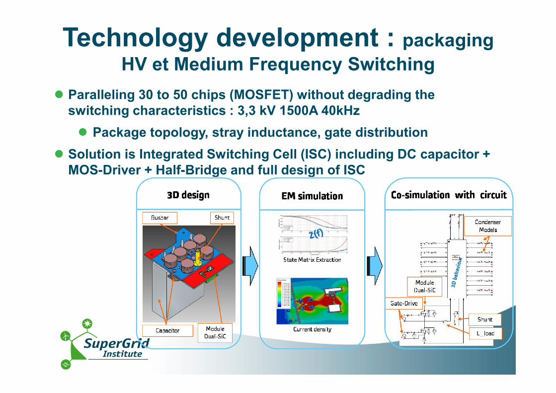
Paralleling 30 to 50 chips (MOSFET) without degrading the switching characteristics : 3,3 kV 1500A 40kHz
Package topology, stray inductance, gate distribution
Solution is Integrated Switching Cell (ISC) including DC capacitor + MOS-Driver + Half-Bridge and full design of ISC
Technology development : packaging
HV et Medium Frequency Switching

LCC valves = series association of thyristors in « press-pack » technology
Very high availability due to automatic reconfiguration of series association in case of component failure = « fail to short » characteristic of press pack technology
It is a « must » to have this feature for HV SiC packaging :
In depth FMEA (Failure Mechanisms and Effect Analysis) of SiC technology mandatory = definition and test of « fail to short » for SiC devices
« Wire bond » lead to low I2t = double side soldering or « Press pack » solution to be adapted
Technology development : fail-to-short packaging
Existing IGBT BV is operational up to 6,5 kV for module and « press-pack » technology up to 10kV
Industrial experience on 6,5 kV IGBT module shows limitations in life-time and reliability :
Peripheral protection technology
Passivation technology
Packaging material technologies
Solutions for packaging SiC 10kV-15kV will include
Field grading will not be only in and on chips but also extended on packaging
Replacement passivation material for SiC (passivation material with higher di-electric strength)
Technology development : solutions for high voltage packaging (10kV-15kV)

Presentation Supergrid Institute
Applications : VSC HVDC & DCDC HVDC-MVDC
Energy efficiency : potential of SiC devices
Prospective on high voltage SiC devices
Conclusion
32
Overview

In 1880, a journalist of Herald Tribune interviewed Thomas Edison about the light bulb and he said :
“After the electric light goes into general use, none but the extravagant will burn tallow candles.”
This affirmation has been transformed into :
“We will make electricity so cheap that only the rich will burn candles”
In 2015, we would like to hear:
“We will make the SiC power chip so cheap, none but the extravagant will continue to use silicon power chip”
33
Conclusion
Penser les réseaux électriques du futur
Soon : www.supergrid-institute.com