Embed Size (px)
Citation preview

Advanced physical modelling of step graded Gunn
Diode for high power TeraHertz Sources
A thesis submitted to The University of Manchester for the degree of
Doctor of Philosophy
in the Faculty of Engineering and Physical Sciences
2011
FAISAL AMIR
SCHOOL OF ELECTRICAL AND ELECTRONIC ENGINEERING

TABLE OF CONTENTS
TABLE OF CONTENTS .......................................................................................... 2
LIST OF FIGURES .................................................................................................. 6
LIST OF TABLES .................................................................................................. 12
LIST OF ABBREVIATIONS................................................................................... 13
ABSTRACT ........................................................................................................... 15
DECLARATION ..................................................................................................... 17
COPYRIGHT STATEMENT ................................................................................... 17
ACKNOWLEDGEMENTS ..................................................................................... 18
DEDICATION ......................................................................................................... 19
Chapter 1 Introduction ........................................................................................ 20
1.1 Project Overview ................................................................................. 20
1.2 Project Motivation ................................................................................ 20
1.3 Research Papers ................................................................................. 21
1.4 Prizes / Awards .................................................................................... 23
1.5 Thesis Organization ............................................................................. 24
Chapter 2 Terahertz Generation and Applications ............................................ 26
2.1 Introduction .......................................................................................... 26
2.2 The Terahertz (THz) Spectrum ............................................................ 27
2.3 THz Generation ................................................................................... 29
2.4 Solid State two Terminal Active Devices for Terahertz Generation ..... 29
2.4.1 Transferred Electron Devices (Gun Diodes) ............................................................29
2.4.2 Tunnelling Devices ...................................................................................................32
2.4.3 Transit – Time Diodes ..............................................................................................32
2.5 Monolithic Microwave Integrated Circuit (MMIC) ................................. 33
2.6 Applications of THz Sources ................................................................ 34
2.6.1 THz Space Applications ...........................................................................................34
2.6.2 THz Security Applications ........................................................................................35
2.6.3 THz Imaging and Spectroscopy Systems ................................................................35
2.6.4 Communications Systems ........................................................................................36
2.6.5 MM-Wave Automotive RADAR Systems .................................................................36
2.6.6 MM-Wave RADAR Industrial Applications ...............................................................36
2.7 Conclusion ........................................................................................... 37
2

3
Table of Contents
Chapter 3 Multiplier and Harmonic generation for Terahertz frequency ........ 38
3.1 Introduction .......................................................................................... 38
3.2 Gunn Diode Oscillator Design ............................................................. 38
3.2.1 Gunn Diode Operation and Hot-Electron Injection ...................................................41
3.2.2 Gunn Diode Electromagnetic Modelling ...................................................................43
3.2.3 Accounting for Interaction between the Diode and Oscillator Circuit .......................45
3.2.4 Proposed Modelling Techniques ..............................................................................47
3.3 Frequency Multipliers ........................................................................... 49
3.3.1 Harmonic Balance Simulation Tool ..........................................................................51
3.3.2 Linear EM Structure Simulations ..............................................................................53
3.3.3 Semiconductor Component – Schottky Diode Varactor ...........................................53
3.4 Schottky Diode SILVACOTM Modelling ................................................ 56
3.5 Conclusion ........................................................................................... 60
Chapter 4 Gunn Diode Theory ............................................................................ 61
4.1 Introduction .......................................................................................... 61
4.2 Gunn Diode as Transferred Electron Effect (TED) Device ................... 61
4.2.1 Electric Field Effects on Electron Drift Velocity ........................................................61
4.2.2 High Field Transport in n-GaAs ................................................................................64
4.2.3 Negative Differential Resistance (NDR) ...................................................................65
4.2.4 Conditions for Negative Differential Mobility ............................................................67
4.3 Instability and Domain Formation ........................................................ 67
4.3.1 Domain Dynamics ....................................................................................................69
4.3.2 Device Oscillating Frequency ...................................................................................72
4.3.3 The Doping – Length (NDL) Product .........................................................................72
4.3.4 Stable Operating Point of Domain ............................................................................73
4.4 Conventional Gunn Diode .................................................................... 75
4.4.1 Temperature Effects on Conventional Gunn Diode .................................................76
4.4.2 Limitations of the Conventional Gunn Diode ............................................................77
4.5 Gunn Diode Oscillation Modes ............................................................ 78
4.5.1 Transit Time Mode ...................................................................................................78
4.5.2 Delayed Domain mode .............................................................................................80
4.5.3 The Quenched Domain Mode ..................................................................................80
4.5.4 Low Space-charge Accumulation (LSA) mode ........................................................81
4.5.5 Operating Modes Summary .....................................................................................82
4.6 Conclusion ........................................................................................... 83
Chapter 5 Advanced GaAs Gunn Diodes with Graded AlGaAs Hot Electron
Injection ................................................................................................................ 84
5.1 Introduction .......................................................................................... 84
5.2 AlGaAs/GaAs Graded Gap Heterostructure ........................................ 85
5.3 Hot Electron Injection........................................................................... 86
5.3.1 The Graded Gap Hot Electron Injector Concept ......................................................86
5.3.2 The AlGaAs/GaAs Hot Electron Injector ..................................................................87
4
Table of Contents
5.4 I-V Characteristics of graded gap injector GaAs Gunn Diode .............. 89
5.4.1 High Frequency Investigations of GaAs Gunn Diodes .............................................90
5.4.2 Hot Electron Injector Barrier Height..........................................................................90
5.4.3 Doping Spike ............................................................................................................91
5.5 Drift Velocity Computation and Operation Mode Classification ............ 93
5.6 Conclusion ........................................................................................... 94
Chapter 6 Gunn Diode Model developments ..................................................... 96
6.1 The SILVACOTM TCAD Suite ............................................................... 96
6.2 Development of the Simulation Model ................................................. 99
6.2.1 High Speed Heterostructure Graded Gap Injector Gunn Diode ...............................99
6.2.2 Gunn Diode 2D Model ..............................................................................................99
6.2.3 2D Model with Heat Sink ........................................................................................103
6.2.4 3D Rectangular Model Development .....................................................................104
6.2.5 3D Cylindrical Model Development ........................................................................105
6.3 Initial Device Solution ........................................................................ 106
6.3.1 DC Simulation Results ...........................................................................................107
6.3.2 Transient solutions .................................................................................................107
6.3.3 Transient Response – free running oscillations .....................................................108
6.4 Free-running frequency of oscillation ................................................. 110
6.5 Conclusion ......................................................................................... 112
Chapter 7 Physical Models................................................................................ 114
7.1 Physical Models Used for Device Simulation ..................................... 114
7.2 Mobility Models Used ......................................................................... 115
7.2.1 Low field Mobility Models .......................................................................................116
7.2.2 AlGaAs Default Low field Mobility Model ...............................................................117
7.2.3 GaAs Concentration Dependent Low Field Mobility Model ....................................118
7.2.4 GaAs Analytic Low Field Mobility Model ................................................................118
7.2.5 Parallel Electric Field Dependent Mobility Model ...................................................119
7.3 Carrier Generation – Recombination Models ..................................... 121
7.3.1 Shockley-Read-Hall (SRH) Recombination ...........................................................121
7.3.2 SRH Concentration-Dependent Lifetime model .....................................................122
7.4 Carrier Statistics and Transport ......................................................... 123
7.4.1 Drift Diffusion Model ...............................................................................................124
7.4.2 The Energy Balance and Hydrodynamic Transport Models ..................................124
7.5 GIGATM – Self Heating Simulator ....................................................... 125
7.5.1 The Lattice Heat Flow Equation .............................................................................126
7.5.2 Heat Capacity .........................................................................................................127
7.5.3 Thermal Conductivity ..............................................................................................128
7.5.4 Heat Generation .....................................................................................................129
7.5.5 Electron Energy Relaxation Time ...........................................................................130
7.5.6 Thermal Boundary Conditions ................................................................................131
7.6 C-Interpreter Functions ...................................................................... 132
7.7 Conclusion ......................................................................................... 133

5
Table of Contents
Chapter 8 Gunn diode Results: DC Analysis ................................................... 134
8.1 Introduction ........................................................................................ 134
8.2 Advanced Step Graded Gunn Diode Modelled–Measured Results ... 134
8.2.1 Doping Spike Carrier Concentration.......................................................................135
8.2.2 DC I-V Characteristics of 77 GHz second Harmonic GaAs Gunn .........................136
8.3 Doping Spike Effects ......................................................................... 136
8.4 Measured 77 GHz Devices Data Comparison with Modelled Devices139
8.4.1 Doping Spike CC 1×10¹⁶
cm-3
Modelled Device Results (VMBE 1928A) ..............139
8.4.2 Doping Spike CC 5×10¹⁷
cm-3
Modelled Device Results (VMBE 1900) .................141
8.4.3 Doping Spike CC 7.5×10¹⁷
cm-3
Modelled Device Results (VMBE 1909) ..............142
8.5 Higher Frequency Measured–Modelled DC I-V Characteristics ........ 144
8.5.1 1.65 µm Transit Region Device DC Results (VMBE 1901 – 77 GHz Device) .......145
8.5.2 1.1 µm Transit Region Device DC Results (VMBE 1950 - 125GHz Device) .........146
8.5.3 0.9 µm Transit Region Device DC Results (VMBE 1897- 125 GHz Device) .........147
8.5.4 0.7 µm transit region device DC results (VMBE 1898 - 100GHz device) ..............148
8.5.5 0.4 µm Transit Region Device DC Results (XMBE 189 – 200 GHz Device) .........149
8.6 Conclusion ......................................................................................... 151
Chapter 9 Gunn diode Results: Time-domain analysis .................................. 153
9.1 Time-Domain (Transient) Solutions ................................................... 153
9.2 Time-Domain Analysis of various Epitaxial Structures....................... 153
9.2.1 1.65 µm Transit Region Device Results (VMBE1901) ...........................................154
9.2.2 1.1 µm Transit Region Device Results (VMBE1950) .............................................155
9.2.3 0.9 µm Transit Region Device Results (VMBE1897) .............................................156
9.2.4 0.7 µm Transit Region Device Results (VMBE1898) .............................................156
9.2.5 0.4 µm – 0.6 µm Transit Region Device Results (XMBE189) ................................158
9.3 Time-Domain Response with a Resonant Cavity .............................. 159
9.3.1 Dipole Domain Formation .......................................................................................159
9.3.2 Modelled Device with Resonant Cavity Time-Domain Results ..............................161
9.4 Conclusion ......................................................................................... 161
Chapter 10 Conclusion and future work .......................................................... 163
10.1 Conclusions ....................................................................................... 163
10.2 Directions for Future Research .......................................................... 165
10.2.1 Lumped Element Model for SILVACOTM
............................................................166
10.2.2 Taking into account Gunn Diode Domain Growth and Propagation ..................166
Appendix – A ...................................................................................................... 168
Appendix – B ...................................................................................................... 174
Appendix – C ...................................................................................................... 177
References.......................................................................................................... 179
Words count, including footnotes and endnotes: 36,822

LIST OF FIGURES
Fig. 2.1 Attenuation due to atmospheric absorption at microwave and mm-
wave frequencies. At mm-wave range, attenuation not only increases, but
becomes more dependent upon absorbing characteristics of H2O & O2.. ... 27
Fig. 2.2 TeraHertz (THz) Gap ..................................................................... 28
Fig. 2.3 Compilation of published state-of-the-art results between 30 and 400
GHz for GaAs and InP Gunn diodes under CW operation. Legend format:
‘mode of operation (‘1’ denotes fundamental, ‘2’ second-harmonic, etc.),
package type, heatsink technology’. Solid lines outline the highest powers
and frequencies achieved experimentally to-date from each material in
fundamental and second-harmonic. ............................................................ 31
Fig. 2.4 Typical Advanced Gunn Diode Structure ........................................ 31
Fig. 3.1 Simplified schematic of the mechanical outline of a second harmonic
resonant disk Gunn diode oscillator. ........................................................... 39
Fig. 3.2 Equivalent electrical circuit model of a second harmonic resonant
disk Gunn diode oscillator. .......................................................................... 39
Fig. 3.3 (a) Ansoft HFSSTM model of a second harmonic resonant disk
millimetre-wave oscillator with tuning pin and circular waveguide sliding
backshort. (b) Simulated field electric field plot for the oscillator at second
harmonic frequencies. ................................................................................ 44
Fig. 3.4 Ansoft HFSSTM simulations of a reduced-height waveguide model
developed at e2v (a) second harmonic resonant disk millimetre-wave
oscillator (b) simulated field electric field plot. ............................................. 45
Fig. 3.5 Gunn diode packages developed at e2v (a) Standard Alumni
Packages (b) Quartz Package.(c) Power Combining .................................. 45
Fig. 3.6 Frequency multiplier design methodology developed at e2v showing
both hydrodynamic and liner electromagnetic structure modelling. ............ 50
6

7
List of Figures
Fig. 3.7 A harmonic balance simulation tool schematics created using
Microwave Office ® by AWR, specifically for analysis and prediction of GaAs
Schottky diode performance given device’s basic electrical characteristics.52
Fig. 3.8 Result of a harmonic balance parametric sweep to study output
power with variation in input embedding impedance .................................. 52
Fig. 3.9 (a) Varactor Diode Chip and the waveguide circuit model created
using HFSSTM at e2v Technologies Plc (b) HFSSTM diode chip model
embedded in waveguide diode mount. ....................................................... 53
Fig. 3.10 2D GaAs diode structure topped by a heavily doped region of InxGa1-
xAs graded from x=0 at the GaAs interface to x=0.53 at the upper surface. 54
Fig. 3.11 (a) C-V plot of 4 µm Schottky device. Junction capacitance of
fabricated single anode device (bias - 1/Cj02 inset) (b) image of a 4 µm
Schottky device with 2 µm bridge to the anode........................................... 55
Fig. 3.12 Six anode anti-series device (a) design (b) fabricated device. ......... 56
Fig. 3.13 GaAs Schottky diode SILVACOTM 2D model. Equal area rule was
maintained same as the manufactured device (a) 2D device structure for a 4
µm diameter anode Schottky diode (b) Conduction band diagram for GaAs
Schottky contact (c). Conduction band diagram at zero bias ...................... 57
Fig. 3.14 Forward bias I-V curve for a 4 µm diameter anode Schottky diode.
Series resistance sR
was calculated from curve’s slope. ............................ 57
Fig. 3.15 C-V plot for a 4 µm diameter anode Schottky diode ......................... 58
Fig. 3.16 Schottky diode C-V plots for 14 µm, 13 µm, 12 µm anode dia.. ....... 59
Fig. 4.1 Carrier Drift Velocity verses Electric Field graph ............................. 63
Fig. 4.2 Electron occupations for (a) GaAs, (b) InP and (c) GaN ................ 63
Fig. 4.3 Electron occupations under various Electric Field levels - n-GaAs 65
Fig. 4.4 Negative Differential Resistance region .......................................... 66
Fig. 4.5 Stable dipole domain formation with the space-charge growth ....... 69
Fig. 4.6 Dynamic characteristics curve and electron drift velocity – electric
field curve plotted in SILVACO using MOCASIM for GaAs 1.1x10⁻¹⁶ doped.
Equal area relationship between Pε and
Rv is shown. ............................... 70

8
List of Figures
Fig. 4.7 Zero Diffusion Domain profiles ........................................................ 70
Fig. 4.8 The domain potential Dφ and minimum electric field
Rε ................. 74
Fig. 4.9 Conventional Gunn Diode structure ................................................ 75
Fig. 4.10 GaAs temperature dependant electron drift velocity curves plotted in
SILVACO using MOCASIM for GaAs 1.1x10⁻¹⁶ doped. .............................. 77
Fig. 4.11 Transit Time Mode - I-V and Time Evolution .................................... 79
Fig. 4.12 Delayed Domain Mode- I-V and Time Evolution .............................. 79
Fig. 4.13 Quenched Domain Mode- I-V and Time Evolution ........................... 81
Fig. 4.14 Gunn Diode Operating Modes Summary ......................................... 82
Fig. 5.1 Potential profile of Hot Electron Injector .......................................... 87
Fig. 5.2 (a) Structure of a GaAs Gunn Diode with step graded hot electron
injector (b) Conduction band profile of a Step Graded AlGaAs
heterostructure Gunn Diode. ....................................................................... 88
Fig. 5.3 Typical advanced step graded injector Gunn Diode structure ......... 89
Fig. 5.4 Gunn Diodes I-V characteristics ..................................................... 90
Fig. 5.5 Conductance and Susceptance versus Frequency plot .................. 91
Fig. 5.6 Low voltage I-V characteristics ....................................................... 91
Fig. 5.7 Electron Concentration – without doping spike ............................... 92
Fig. 5.8 Electron Concentration – with doping spike .................................... 92
Fig. 5.9 Diode with Injector ........................................................................... 93
Fig. 5.10 Electrons occupations in the L- valley .............................................. 94
Fig. 6.1 ATLASTM Input-Output hierarchy ..................................................... 97
Fig. 6.2 ATLASTM command groups ............................................................. 98
Fig. 6.3 Gunn Diode model development process flow ................................ 98
Fig. 6.4 77 GHz Gunn advanced step graded injector Gunn Diode str. ....... 99
Fig. 6.5 Graded Gap Heterostructure Gun Diode ....................................... 100
Fig. 6.6 TonyPlotTM of modelled device structure showing impurity doping
profile (a) Device planar view (b) Device cross section view .................... 100

9
List of Figures
Fig. 6.7 Device structure with mesh density defined (a) using ‘constraint’ (b)
using ‘refine’, plotted in TonyPlotTM ........................................................... 101
Fig. 6.8 Conduction band comparative data showing two models with course
and dense meshing in the step-graded launcher ...................................... 102
Fig. 6.9 Modelled device structure with heat sinks ..................................... 103
Fig. 6.10 3D rectangular model epitaxial structure ........................................ 104
Fig. 6.11 3D rectangular modelled device structure with heat sinks ............. 105
Fig. 6.12 3D cylindrical modelled device structure with heat sinks ................ 105
Fig. 6.13 Device model structure cross section view plotted in TonyPlotTM .. 106
Fig. 6.14 Model forward-reverse asymmetrical I-V characteristics ................ 107
Fig. 6.15 Device model transient voltage ramp in ATLASTM ......................... 108
Fig. 6.16 Transient response - critical current at 2V ...................................... 109
Fig. 6.17 Transient response - damping frequency at 2V ............................. 109
Fig. 6.18 Transient response - stable oscillations at 4V ................................ 110
Fig. 6.19 Monte Carlo simulation results for GaAs Gunn diodes with and
without hot electron injection. It is noted that the power curve is taken from
measurements of a typical device with hot electron injection, and that an
oscillator circuit was not included in the simulation. .................................. 111
Fig. 8.1 The effects of the doping spike (cc 1×1018 cm-3) on electron
concentration in the transit region (—; spike present, ----; spike absent) .. 135
Fig. 8.2 Modelled and measured forward - reverse I-V curves................... 136
Fig. 8.3 Electron concentration with changing doping spike cc ................. 137
Fig. 8.4 Effects of variation in doping spike cc on simulated I-V characteristics
(nos next to forward bias curves represent calculated asymmetry values) 137
Fig. 8.5 Simulated - measured asymmetry values versus doping spike cc 138
Fig. 8.6 VMBE1928A Modelled and measured forward-reverse I-V curves 140
Fig. 8.7 VMBE 1928A Temperature forward - reverse I-V curves .............. 140
Fig. 8.8 VMBE 1900 Modelled and measured forward - reverse I-V curves141
Fig. 8.9 VMBE 1900 Temperature forward - reverse I-V curves ................ 141

10
List of Figures
Fig. 8.10 VMBE 1909 Modelled and measured forward - reverse I-V curves 142
Fig. 8.11 VMBE 1909 Temperature forward - reverse I-V curves ................. 142
Fig. 8.12 Simulated-measured asymmetry values versus doping spike cc.143
Fig. 8.13 VMBE 1901 Forward and reverse I-V curves for a 70-80 GHz 2nd
harmonic device at 300K .......................................................................... 145
Fig. 8.14 VMBE 1901 Temperature forward and reverse I-V curves ............. 145
Fig. 8.15 VMBE 1950 Forward and reverse I-V curves for a 62.5GHz
fundamental, 125GHz 2nd harmonic device at 300K ................................. 146
Fig. 8.16 VMBE 1950 Temperature forward and reverse I-V curves ............. 146
Fig. 8.17 VMBE 1897 Forward and reverse I-V curves for a 62.5 GHz
fundamental, 125GHz 2nd harmonic device at 300K ................................. 148
Fig. 8.18 VMBE 1897 Temperature forward and reverse I-V curves ............. 148
Fig. 8.19 VMBE 1898 Forward and reverse I-V curves for a 100 GHz
fundamental device at 300K ..................................................................... 149
Fig. 8.20 VMBE 1898 Temperature forward and reverse I-V curves ............. 149
Fig. 8.21 XMBE 189 Modelled forward and reverse I-V curves. Effects of
variation in doping spike cc on simulated I-V characteristics (numbers next
to forward bias curves represent calculated asymmetry values). Transit
region cc was 5.4 x1016 cm-3. .................................................................... 150
Fig. 8.22 XMBE 189 Modelled forward and reverse I-V curves for a 200 GHz
fundamental device at 300K ..................................................................... 151
Fig. 8.23 XMBE 189 Temperature forward and reverse I-V curves ............... 151
Fig. 9.1 The simulated fundamental frequency time-domain response of a
device fabricated from VMBE1901 (1.65 µm transit length) under a 2.2V
external bias ............................................................................................. 154
Fig. 9.2 The simulated fundamental frequency time-domain response of a
device fabricated from VMBE1901 (1.65 µm transit length) under a 3.2 V
external bias. ............................................................................................ 155
11
List of Figures
Fig. 9.3 The simulated fundamental frequency time-domain response of a
device fabricated from VMBE1950 (1.1 µm transit length) at an external bias
of 2.5V, temperature 300K. ....................................................................... 155
Fig. 9.4 The simulated fundamental frequency time-domain response of a
device fabricated from VMBE1897 (0.9 µm transit length) at an external bias
of 2.2V, temperature 300K. ....................................................................... 156
Fig. 9.5 The simulated fundamental frequency time-domain response of a
device fabricated from VMBE1898 (0.7 µm transit length) at an external bias
of 1.7V, temperature 300K. ....................................................................... 157
Fig. 9.6 The simulated fundamental frequency time-domain response of a
device fabricated from VMBE1898 (0.7 µm transit length) at an external bias
of 2.75 V, temperature 300K. .................................................................... 157
Fig. 9.7 The simulated fundamental frequency time-domain response of a
device fabricated from XMBE189 (0.4 µm transit length) at an external bias
of 3.5V, temperature 300K. ....................................................................... 158
Fig. 9.8 Spatial dipole domain profiles in the transit region, for a 0.7 µm
transit length device. These are plotted at an applied bias of 3V at time,
starting at 0.156ps, in one oscillation period T=4.68 ps. The domain first
grows to a maximum size and then drifts to the anode before it collapses
there and a new domain nucleates. .......................................................... 160
Fig. 9.9 Time-domain stable oscillation at 3 V with Cdiode = 0.158 pF. The
lumped-element LC parallel circuit values are L= 3.16 pH and C= 0.403 pF.
The main loss R=0.9 Ohms is in series with the L. The current overshoot
peaks are in agreement with [9] which are due to electron experiencing
energy and momentum inertial effects at high frequencies. ...................... 161

LIST OF TABLES
Table 2.1 Terahertz terminology ................................................................... 26
Table 3.1 Schottky diode models with 14µm, 13µm and 12µm anode
diameters showing an additional area and calculated cut off frequencies. . 59
Table 7.1 Physical models summary .......................................................... 115
Table 7.2 Mobility values for AlxGa1-xAs regions ....................................... 117
Table 7.3 Caughey Thomas analytic low field mobility model parameters . 119
Table 7.4 GIGATM – self heating simulator parameters .............................. 126
Table 7.5 Heat Capacity parameters .......................................................... 127
Table 7.6 Thermal Conductivity parameters ............................................... 128
Table 7.7 Electron energy relaxation time parameters ............................... 131
Table 7.8 C-Interpreter Functions used in model development .................. 132
Table 8.1 Measured devices with slightly different epitaxial structures –
doping spike carrier concentration variation.............................................. 139
Table 8.2 Measured devices with slightly different epitaxial structures – transit
region length and its carrier concentration variation ................................. 144
Table 9.1 Measured devices with slightly different epitaxial structures – transit
region length and its carrier concentration variation ................................. 153
12

LIST OF ABBREVIATIONS
2D Two Dimensional
ACC Adaptive Cruise Control
ACCS Adaptive Cruise Control Systems
ADS Advanced Design System by Agilent
Technologies
AlAs Aluminium arsenide
AlGaAs Aluminium gallium arsenide
AlSb Aluminium Antimonide
As Arsenic
AWR Advancing the Wireless Revolution
BARITT Barrier Injection Transit Time
CB Conduction band
cc Carrier Concentration
CdTe Cadmium Telluride
CMS Collision Mitigation Systems
CO2 Carbon dioxide
CVD Chemical Vapour Deposition
CW Continuous Wave
DC Direct Current
EM ElectroMagnetic
fF Femto Farad
FMCW Frequency Modulated Continuous Wave
Ga Gallium
GaAs Gallium arsenide
GaAsP Gallium Arsenide Phosphide
GaInAs Gallium Indium arsenide
GaN Gallium Nitride
GHz Gega Hertz
HFSS High Frequency Structure Simulator
IMPATT Impact Ionization Transit Time
InAs Indium arsenide
13

14
List of Abbreviations
Inc Incorporation
InP Indium Posphide
I-V Current-Voltage
K Kelvin
L Satellite
LSA Low Space-charge Accumulation
MBE Molecular Beam Epitaxy
micron micrometre
MITATT Mixed Tunnelling-Avalanche Transit-Time
mm milli metre
MMIC Monolithic Microwave Integrated Circuit
mW milli watt
NDR Negative Differential Resistance
Plc public limited company
RF Radio Frequency
RIE Reactive Ion Etching
RTD Resonant Tunnelling Diode
SI Semi-Insulating
SRH Shockley-Read-Hall
STFC Science and Technology Facilities Council
TADAR Tactical Area Defence Alerting Radar
TCAD Technology Computer-Aided Design
TD Tunnel diode
TDTS Time-domain THz Spectroscopy
TED Transferred Electron Devices
TEM Transverse ElectroMagnetic
THz Terahertz
Ti Titanium
TM Trademark
TUNNETT Tunnel Injection Transit Time
UMS Universal Marking Systems Ltd
VWF Virtual Wafer Fab
ZnSe Zinc Selenide
Γ Gamma

ABSTRACT
The mm-wave frequency range is being increasingly researched to close the gap
between 100 to 1000 GHz, the least explored region of the electromagnetic
spectrum, often termed as the ‘THz Gap’. The ever increasing demand for
compact, portable and reliable THz (Terahertz) devices and the huge market
potential for THz system have led to an enormous amount of research and
development in the area for a number of years. The Gunn Diode is expected to
play a significant role in the development of low cost solid state oscillators which
will form an essential part of these THz systems.
Gunn and mixer diodes will “power” future THz systems. The THz frequencies
generation methodology is based on a two-stage module. The initial frequency
source is provided by a high frequency Gunn diode and is the main focus of this
work. The output from this diode is then coupled into a multiplier module. The
multiplier provides higher frequencies by the generation of harmonics of the input
signal by means of a non-linear element, such as Schottky diode Varactor. A
realistic Schottky diode model developed in SILVACOTM is presented in this
work.
This thesis describes the work done to develop predictive models for Gunn Diode
devices using SILVACOTM. These physically-based simulations provide the
opportunity to increase understanding of the effects of changes to the device’s
physical structure, theoretical concepts and its general operation. Thorough
understanding of device physics was achieved to develop a reliable Gunn diode
model. The model development included device physical structure building,
material properties specification, physical models definition and using
appropriate biasing conditions.
The initial goal of the work was to develop a 2D model for a Gunn diode
commercially manufactured by e2v Technologies Plc. for use in second harmonic
mode 77GHz Intelligent Adaptive Cruise Control (ACC) systems for automobiles.
15

16
Abstract
This particular device was chosen as its operation is well understood and a
wealth of data is available for validation of the developed physical model. The
comparisons of modelled device results with measured results of a manufactured
device are discussed in detail. Both the modelled and measured devices yielded
similar I-V characteristics and so validated the choice of the physical models
selected for the simulations. During the course of this research 2D, 3D
rectangular, 3D cylindrical and cylindrical modelled device structures were
developed and compared to measured results.
The injector doping spike concentration was varied to study its influence on the
electric field in the transit region, and was compared with published and
measured data.
Simulated DC characteristics were also compared with measured results for
higher frequency devices. The devices mostly correspond to material previously
grown for experimental studies in the development of D-band GaAs Gunn
devices. Ambient temperature variations were also included in both simulated
and measured data.
Transient solutions were used to obtain a time dependent response such as
determining the device oscillating frequency under biased condition. These
solutions provided modelled device time-domain responses. The time-domain
simulations of higher frequency devices which were developed used modelling
measured approach are discussed. The studied devices include 77GHz (2nd
harmonic), 125 GHz (2nd harmonic) and 100 GHz fundamental devices.
During the course of this research, twelve research papers were disseminated.
The results obtained have proved that the modelling techniques used, have
provided predictive models for novel Transferred Electron Devices (TEDs)
operating above 100GHz.

DECLARATION
No portion of the work referred to in the thesis has been submitted in support of
an application for another degree or qualification of this or any other university or
other institute of learning.
COPYRIGHT STATEMENT
I. The author of this thesis (including any appendices and/or schedules to
this thesis) owns certain copyright or related rights in it (the “Copyright”)
and he has given The University of Manchester certain rights to use such
Copyright, including for administrative purposes.
II. Copies of this thesis, either in full or in extracts and whether in hard or
electronic copy, may be made only in accordance with the Copyright,
Designs and Patents Act 1988 (as amended) and regulations issued
under it or, where appropriate, in accordance with licensing agreements
which the University has from time to time. This page must form part of
any such copies made.
III. The ownership of certain Copyright, patents, designs, trade marks and
other intellectual property (the “Intellectual Property”) and any
reproductions of copyright works in the thesis, for example graphs and
tables (“Reproductions”), which may be described in this thesis, may not
be owned by the author and may be owned by third parties. Such
Intellectual Property and Reproductions cannot and must not be made
available for use without the prior written permission of the owner(s) of the
relevant Intellectual Property and/or Reproductions.
IV. Further information on the conditions under which disclosure, publication
and commercialisation of this thesis, the Copyright and any Intellectual
Property and/or Reproductions described in it may take place is available
in the University IP Policy, The University Library’s regulations and in The
University’s policy on presentation of Theses.
(see http://www.campus.manchester.ac.uk/medialibrary/policies/intellectual-property.pdf),
(see http://www.manchester.ac.uk/library/aboutus/regulations).
17

18
ACKNOWLEDGEMENTS
I would like to thank my supervisor Prof M Missous, for his guidance and
encouragement in the project, which motivated me to learn and develop the skills
for modelling performed using the SILVACOTM software. These physically based
engineering model simulations provided me an opportunity to increase
understanding of changes to the device physical structure, theoretical concepts
and its general operation. Thanks also to Dr. Novak Farrington who remained
involved with the research work and provided the best possible help and support.
His valuable time spent on different aspects of project discussions, provision of
experimentally measured data and suggestions for the write-up resulted in high
quality research.
I would like to thank the M&N group PhD students performing semiconductor
device modelling for their encouragement, motivation and assistance when
required during the device model development phase.
The National University of Sciences and Technology (NUST, Pakistan) is greatly
acknowledged for supporting my PhD studies under ‘faculty development
programme’. Thanks to my supervisor who arranged finances from the School of
Electrical and Electronic Engineering (E&EE) and M&N Group, which allowed me
to remain focused and achieve research goals. Thanks are also due to the IEEE
Electron Devices Society for the award of a PhD fellowship in August 2009.
Thanks are also due to Mike Carr (e2v Technologies Plc, UK) for providing the
experimentally measured data for the Gunn diodes.

19
DEDICATION
This thesis is dedicated to my family.
In particular to my
caring parents and beloved wife Fatima.
gorgeous daughter Farheen Wardah and
adorable son Muhammad Daud, both born
during the course of this research work

Chapter 1 Introduction
1.1 Project Overview
The aim of this project was to develop a physical model for an advanced GaAs
hot electron injector Gunn diode to be used as a high power terahertz source.
The physically-based model has been developed in SILVACOTM, Inc.-TCAD
(Technology Computer-Aided Design) using the ATLASTM Virtual Wafer FabTM
(VWFTM) device simulation software. The model I-V simulation response was
then compared to the fabricated devices measured data to validate the various
models used during simulations and their associated material parameters. The
injector performance was evaluated and the effects of doping spike carrier
concentration were studied. Time domain transient simulations were performed
to determine modelled devices operating frequency and to investigate transit
length scaling effects on device performance.
A Schottky diode 2D model was also developed in ATLASTM to study the
underlying device physics and extract parameters to be used in harmonic
balance simulations created using Microwave Office ® by AWR (Advancing the
Wireless Revolution) Corporation.
1.2 Project Motivation
The research work was undertaken as part of the STFC (Science and
Technology Facilities Council) funded project, ‘High Power Semiconductor
Terahertz Frequency Sources for Imaging Applications’. The research was aimed
at accessing the THz region through the use of high frequency Gunn diodes in
conjunction with frequency multipliers. The project was a joint collaboration
between The University of Manchester (UoM) and e2v Technologies (UK) Plc.
The main objective of this project was to design, fabricate and test the
components (Gunn diodes and multipliers) covering the range 100 to 600 GHz.
This was planned to be achieved by the development and delivery of high power
graded gap Gunn diodes with measurable output of at least 20 to 40 mW at 200
20

21
Chapter 1 Introduction
GHz and novel multipliers sources with overall efficiency of at least 5% for 600
GHz operation.
e2v Technologies (UK) Plc have been working on step-graded gap diodes for
automotive applications at 77 GHz for over a decade whilst developing
technologies to increase the operational frequency of these GaAs devices to well
over 100 GHz [13].
This research work presented here is focused on predictive modelling of Gunn
diodes using the SILVACOTM software package. The developed model was
ruggedly tested against actual data at 77GHz to demonstrate its worth to forming
a bench mark for future predictive device modelling and research. It was then
used as the basis for predicting the response and performance characteristic of
higher frequency Gunn diodes prior to their fabrication. The model proved to be
an extremely useful tool for the optimisation of the required epitaxial structures.
1.3 Research Papers
The following papers have been presented during the course of this research
work.
1. N. Farrington, F. Amir, J. Sly and M. Missous, ‘SILVACO modelling of a
Gunn diode with step-graded hot-electron injector, and pulsed DC testing of on-
wafer quasi-planar mm-wave Gunn diode structures’, 16th European Workshop
on Heterostructure Tech., HETECH’07, 2-5 Sept 07, Fréjus, France, pp. Tu2-7.
Research undertaken as part of MSc Dissertation project ‘Terahertz (THz)
Sources for Space and Security Applications’.
http://www.crhea.cnrs.fr/hetech07/index.htm
2. F. Amir, N. Farrington, J. Sly and M. Missous, ‘Step-graded Hot Electron
Injector Gunn Diode Modelling in SILVACO’, Workshop on Theory, Modelling
and Computational Methods for Semiconductor Materials And Nanostructures,
31 Jan – 1 Feb 08, The University of Manchester, UK.
http://www.eee.manchester.ac.uk/research/groups/mandn/docs/abstractsv3.pdf

22
Chapter 1 Introduction
3. F. Amir, N. Farrington, J. Sly and M. Missous, 'Physical Modelling of a
GaAs Gunn Diode with a Step-graded AlGaAs Hot Electron Injector', UK
semiconductors 2008, 2-3 Jul 08, University of Sheffield, Sheffield, UK.
http://www.uksemiconductors.com/
4. F. Amir, N. Farrington, T. Tauqeer, M. Missous, ‘Physical Modelling of a
Step-Graded AlGaAs/GaAs Gunn Diode and Investigation of Hot Electron
Injector Performance’, Advanced Semiconductor Devices and Microsystems,
2008. ASDAM 2008. International Conference pp.51-54, 12-16 Oct 08.
http://ieeexplore.ieee.org/xpls/abs_all.jsp?arnumber=4743356
5. T. Tauqeer, J. Sexton, F. Amir, M. Missous, ‘Two-Dimensional Physical
and Numerical Modelling of InP-based Heterojunction Bipolar Transistors,’
Advanced Semiconductor Devices and Microsystems, 2008. ASDAM 2008.
International Conference, pp.271-274, 12-16 Oct 08.
http://ieeexplore.ieee.org/xpls/abs_all.jsp?arnumber=4743335
6. F. Amir, N. Farrington, T. Tauqeer and M. Missous, ‘A Novel Physical
Model Developed of an Advanced Cylindrical Step Graded Heterostructure mm-
wave Gunn Diode’, 17th European Workshop on Heterostructure Technology,
HETECH’07, 2-5 Nov 08, Venice, Italy.
http://www.hetech2008.org/
7. F. Amir, C. Mitchell, N. Farrington and M. Missous, ‘Advanced Step-
graded Gunn Diode for mm-wave Imaging Applications’, 5th ESA Workshop on
Millimetre Wave Technology and Applications and 31st ESA Antenna
Workshop, 18-20 May 09, ESTEC, Noordwijk, The Netherlands, pp. 201-205.
http://www.congrex.nl/09c05/
8. T. Tauqeer, J. Sexton, M. Mohiuddin, R. Knight, F. Amir and M.
Missous, 'Physical modelling of base-dopant out diffusion in Single
Heterojunction Bipolar Transistors', UK semiconductors 2009, 1-2 Jul 09,
University of Sheffield, Sheffield, UK.
http://www.uksemiconductors.com/

23
Chapter 1 Introduction
9. F. Amir, C. Mitchell, N. Farrington and M. Missous, ‘Advanced Gunn
Diode as High Power Terahertz Source for a Millimetre Wave High Power
Multiplier’, SPIE Europe Security + Defence 2009, 31 Aug to 03 Sept 09,
Berliner Congress Centre, Berlin, Germany, Proc. SPIE, vol. 7485, pp 748-50I.
http://spie.org/x648.html?product_id=830296
10. F. Amir, C. Mitchell, N. Farrington, T. Tauqeer and M. Missous,
‘Development of Advanced Gunn Diodes and Schottky Multipliers for High
Power THz sources’, 2nd UK/Europe-China Workshop on Millimetre Waves and
Terahertz Technologies, 19-21 Oct 09, Rutherford Appleton Laboratory (RAL),
Oxford, UK pp. 80.
http://www.sstd.rl.ac.uk/mmt/ukchinathz2009.php
11. F. Amir, N. Farrington, C. Mitchell and M. Missous, ‘Time-domain
analysis of sub-micron transit region GaAs Gunn diodes for use in Terahertz
frequency multiplication chains’, SPIE Europe Security + Defence 2010, SD108
‘Millimetre Wave and Terahertz Sensors and Technology’ (Session I - Millimetre
and THz Devices), 20-23 Sept 10, Centre de Congrès Pierre Baudis, Toulouse,
France. Proc. SPIE 7837, 783702 (2010).
http://spie.org/x648.html?product_id=864872
12. F. Amir, C. Mitchell and M. Missous, ‘Development of Advanced Gunn
Diodes and Schottky Multipliers for High Power THz sources’, Advanced
Semiconductor Devices and Microsystems (ASDAM), 2010. 8th International
Conference, Smolenice, Slovakia, 25-27 Oct 10, pp. 29-32.
http://ieeexplore.ieee.org/xpls/abs_all.jsp?arnumber=5667005
1.4 Prizes / Awards
a. MSc Dissertation project ‘Terahertz (THz) Sources for Space and Security
Applications’, research work adjudged best in the class and presented in 16th
European Workshop on Heterostructure Technology (HeTech 07) held in Nice,
France, September 2007.
24
Chapter 1 Introduction
b. Awarded 2009 IEEE EDS PhD Student Fellowship representing entire
region 8 (Europe, Africa and Middle-East), for the demonstration of significant
ability to perform independent research in the field of electron devices and a
proven record of academic excellence.
http://eds.ieee.org/eds-phd-student-fellowship-program.html
c. The fellowship award was announced in January 2010 issue of EDS
newsletter. A brief research progress report was published in July 2010 issue.
http://eds.ieee.org/eds-newsletters.html
d. Awarded 1st Prize during Post Graduate Research (PGR) Poster
Conference 2009 at The University of Manchester, School of E&EE.
http://www.eee.manchester.ac.uk/research/pgr_conference/pgrconf09/
e. SPIE Europe Security + Defence 2009 Symposium’s paper ‘Advanced
step-graded Gunn diode for millimetre applications’ was published on the SPIE
Newsroom page http://spie.org/x36521.xml?highlight=x2404&ArticleID=x36521.
f. In February 2010, nominated for the 2010 University of Manchester
Distinguished Achievement Awards in category ‘Postgraduate Research Student
of the year’, representing the School of E&EE, The University of Manchester.
1.5 Thesis Organization
The organization of the remainder of this thesis is as follows:
Chapter 2 briefly covers Terahertz technology and its applications with an
emphasis on Gunn diodes. The multiplier and harmonic generation methodology
is covered in Chapter 3. Chapter 3 presents an oscillator cavity developed in
HFSSTM at e2v. The harmonic balance simulation tool created in Microwave
Office ® by AWR is discussed and both semiconductor components of the
multiplier are also presented. Chapter 4 provides a detailed account of
conventional Gunn diode theory with an explanation of the Negative Differential
Resistance (NDR) effects, which depends on the bulk material properties.

25
Chapter 1 Introduction
Various device operating modes are presented with emphasis on the high
frequency oscillations before summarizing the limitations of conventional Gunn
diode. Chapter 5 will discus the concept and theory behind the hot electron
injector. It would provides a literature survey of the step graded hot electron
injector Gunn diode that has been developed to overcome the limitations of the
conventional Gunn diode. Chapter 6 will provide a step-by-step process used to
develop a model in SILVACOTM. Chapter 7 would outline device physical models
and discusses them in detail along with the material parameters used. Gunn
diode DC I-V characteristics that are compared to the measured results will be
presented in chapter 8. The doping spike carrier concentration optimization is
also presented. Chapter 9 will discuss Gunn diode Time-domain analyses. Also
presented would be the results of a novel 100 GHz fundamental device that has
been simulated in an oscillator cavity. Chapter 10 will provide the conclusion and
summary of the Gunn diode modelling work. It also gives a brief account of
proposed future research work.
The appendices of this thesis contain SILVACOTM codes.

Chapter 2 Terahertz Generation and Applications
2.1 Introduction
The Terahertz (THz) spectrum is being increasingly researched to close the
frequency gap between microwaves and infrared. The THz region, typically
referred to as the frequencies from 100 GHz to 10 THz, is the least explored
region of the electromagnetic spectrum, often termed as the ‘THz Gap’. Table 1
list the common terminologies used to describe the frequency bands within this
gap.
Frequency Wavelength Used term
30 to 300 GHz 10 mm to 1 mm Millimetre
300 GHz to 3 THz 1 mm to100 µm Sub millimetre [14]
100 GHz to 10 THz 3 mm to 30 µm Terahertz [15]
3 to 30 THz 100 µm to 10 µm Far infrared
Table 2.1 Terahertz terminology
THz waves can penetrate through dielectric materials such as fabrics, plastics
and cardboard, which makes it an ideal choice to replace X-ray imaging and
ultrasound imaging for security applications such as detecting concealed objects.
Its non-ionizing properties and lower photon energy levels, milli-electron volt,
makes it safe for people during security checks, inspection of various biological
samples, etc. At THz frequencies the living tissues are semi-transparent and
have ‘terahertz fingerprints’, permitting them to be imaged, identified, and
analyzed. THz spectral imaging technology not only differentiates objects
morphology, but it also identifies their composition. Additionally, it provides
higher spatial resolution, and therefore an ideal choice for non-destructive
testing.
THz radiation has higher frequency and bandwidth that provides short-distance
high-capacity wireless communications. An increasingly widespread application
is automotive FMCW (Frequency Modulated Continuous Wave) radar in the low
26

27
Chapter 2 Terahertz Generation and Applications
atmospheric attenuation window at 77GHz (Fig. 2.1). The unique characteristics
of THz radiation have important applications in the field of astrophysics, plasma
physics, materials science, information science and engineering etc.
The demand for high-frequency, high output power device technology has
increased enormously in the past decade due to an array of emerging
applications, which has resulted in focused and intense research in the field. This
has led to an interest in the development of Physically-based models to aid in the
development of next generation devices.
The Gunn Diode has long been considered the heart of mm-wave power
generation. However, in recent years Monolithic Microwave Integrated Circuit
(MMIC) solutions for power generation at mm-wave frequencies have become
commercially viable but suffer from high cost and low output power levels as
discussed later.
2.2 The Terahertz (THz) Spectrum
As shown in Fig. 2.2, THz frequencies correspond to photon energy levels from
approximately 4 to 40 milli-electron volts or to an equivalent black body
temperature between 50 and 500 Kelvin. The frequency range spans 100 GHz to
Fig. 2.1 Attenuation due to atmospheric absorption at microwave and millimetre wave frequencies [7]. At millimetre wave range, the attenuation not only increases, but becomes more dependent upon absorbing characteristics of H2O and O2.

28
Chapter 2 Terahertz Generation and Applications
10 THz, which corresponds to wavelengths 3 mm to 30 µm [16]. The potential
applications for THz devices have increased many fold during the past few years
and range from security radar to medical imaging for tumour detection [17]. Other
potential applications include high bandwidth communications, high resolution
radar systems, security imaging systems and space exploration.
The transition from electronics to optics takes place in the infrared region of the
electromagnetic spectrum where the wavelengths are less than 1mm. The lower-
frequency region of the infrared is known as ‘far infrared’ and is generally
considered as extension of the microwave region. Originally, the edge of the
microwave band (300 GHz) was considered the highest viable frequency for
electronics, but as technology has progressed, the limits of electronics have
been pushed further into the infrared. However, the lower efficiency of both
optical and electronic devices in the THz region has been a big impediment in
the development of Terahertz systems. Therefore, research has been focused on
the THz gap (Fig. 2.2) with aims to improve device efficiency and increase its
output power levels [15]. In optics, apart from a few electron lasers, which
reached the kilowatt power range [18], other laser sources are limited to milliwatt
and microwatt power levels [8]. In electronics fabrication of 77 & 125 GHz
systems using Gunn diode & MMIC technology have been developed. Although
these currently operate in the mm-wave frequency range, they are being
researched to extend in to the THz region [19].
Fig. 2.2 TeraHertz (THz) Gap [8]

29
Chapter 2 Terahertz Generation and Applications
2.3 THz Generation
Terahertz sources can be broadly divided into three categories namely, vacuum
tube, optical and solid state sources. The vacuum tube sources are bulky, large
and need huge power to generate substantial electric and magnetic fields and
current densities. Additionally, their physical scaling is very difficult. The optical
sources operate at very low energy levels ~meV. The low energy levels requires
cryogenic cooling due to the effect of lattice phonons [16]. The electronic solid
state sources are preferred for room temperature operation. They are limited due
to parasitics and transit time effects. Their engineering becomes challenging due
to power rolling off exponentially as the frequency increases.
2.4 Solid State two Terminal Active Devices for Terahertz Generation
Millimetre-wave frequencies can be generated using various two-terminal solid
state active devices. The most commonly used devices include Transferred
electron or Gunn diodes (TEDs) [20], Esaki tunnel diodes (TDs) [21], resonant
tunnelling diodes (RTDs) [22] and transit-time diodes. The transit-time diodes
includes Impact Ionization Transit Time (IMPATT) [23], Barrier Injection Transit
Time (BARITT) [24], Tunnel Injection Transit Time (TUNNETT) [25] and Mixed
Tunnelling-Avalanche Transit-Time (MITATT) [26, 27] diodes. All of these
devices display the property of Negative Differential Resistance (NDR).
The transferred electron effect, tunnelling and transit-time diodes are discussed
next;
2.4.1 Transferred Electron Devices (Gun Diodes)
The Gunn Diode named after J. B. Gunn [20] who discovered the effect named
after him, is an active solid state two terminal device, classed as a Transferred
Electron Device (TED). The most conspicuous feature of the device is the
negative differential resistance, which depends on bulk material properties [28].
The Gun diode in its basic form is a homogenous two terminal device with an
ohmic contact at each end. The device has a sandwich-like structure and

30
Chapter 2 Terahertz Generation and Applications
comprises of n+-n-n+ semiconductor materials and is commonly grown using
Molecular Beam Epitaxy (MBE). GaAs and InP are the most commonly used
material systems although other materials such as CdTe, ZnSe, GaAsP and GaN
may possibly also exhibit the transferred electron effect and are being
researched for use at higher frequencies [29]. State of the art GaAs and InP
Gunn diode output powers, and DC to RF conversion efficiencies are shown in
Fig. 2.3. It can be seen that the output power of Gunn devices falls rapidly with
the increase in frequency due to material limitations such as energy relaxation
time. Generally two or more diodes are employed in conjunction with a frequency
multiplier to achieve frequency generation above the fundamental limit e.g. from
200 GHz to 1 THz, with power levels of 0.1 to 1 mW at 400 GHz [6] being
achieved.
Although GaAs or InP Gunn diode devices are simple in physical structure, they
require extreme care during growth for optimization of physical parameters such
as doping concentration and device length. The ohmic contact resistance needs
to be as small as possible, as this can significantly affect device resistance and
thus has considerable effect on the device operating frequency range. Devices
operating in W-band (60 to 110 GHz) have typically specific contact resistivity
values of less than 6 25 10 cm− −× Ω , while for W-band and above (i.e. above 110
GHz) values of specific contact resistivity of 7 25 10 cm− −× Ω or less are required
[30].
GaAs Gunn diodes currently being commercially fabricated provide moderate
power levels of typically around 60 mW at 94 GHz for GaAs in second harmonic
mode [31]. Due to low phase noise (-88 dBc / Hz at 100 KHz offset) at mm-wave
frequencies, Gunn diodes are considered extremely suitable for Frequency
Modulated Continuous Wave (FMCW) radar and imaging systems. However, the
biggest problem of the Gunn diode is its low DC-to-RF conversion efficiency and
associated high operational temperatures. Due to the high cost associated with
device fabrication, physically-based predictive modelling can be used to
complement experimentally verified devices. A typical model of an advanced
Gunn Diode developed at Manchester, and used in commercial Adaptive Cruise
Control Systems (ACCS) in BMW and Audi cars, is shown in Fig. 2.4.

31
Chapter 2 Terahertz Generation and Applications
Do
pin
g C
on
cen
tratio
n e
xce
pt
lau
nch
er
Co
nta
ct L
aye
r
Gra
de
d A
lGa
As L
au
nch
er
Un
do
ped
Bu
ffe
r
Su
bstr
ate
C
on
tact
Laye
r
Transit Region
Device Depth
Do
pin
g S
pik
e
Hot Electron Injector
Fig. 2.4 Typical Advanced Gunn Diode Structure (not to scale)
Fig. 2.3 Compilation of published state-of-the-art results between 30 and 400 GHz for GaAs and InP Gunn diodes under CW operation. Legend format: ‘mode of operation (‘1’ denotes fundamental, ‘2’ second-harmonic, etc.), package type, heatsink technology’. Solid lines outline the highest powers and frequencies achieved experimentally to-date from each material in fundamental and second-harmonic [6]
30 100 4000.1
1
10
100
1000
RF
Ou
tpu
t P
ow
er
(mW
)
Frequency (GHz)
1, Alumina Ring, IHS
1, Alumina Ring, Diamond
2, Alumina Ring, IHS
3, Package unknown
GaAs, InP
GaA
s fu
nd
am
en
tal
InP fundamental
InP
2nd h
arm
onic
GaA
s 2
nd
harm
onic
1
1
1
1 denotes e2v technologies result
with hot-electron injection
No
vak E
. S
. F
arr
ing
ton
, e2v t
ech
no
log
ies, L
inco
ln, U
K, S
ep
tem
ber
2009
1
1, Open Quartz, IHS
1, Open Quartz, Diamond
2, Quartz Ring, IHS
2, Open Quartz, Diamond
2, None, IHS
2, None, Diamond
3, None, IHS

32
Chapter 2 Terahertz Generation and Applications
2.4.2 Tunnelling Devices
Both Esaki Tunnel diodes (TDs) [21] and Resonant Tunnelling Diodes (RTDs)
[22] fall under this category. These devices generate oscillations by exhibiting
negative differential resistance in their I-V characteristics. They are active solid
state two terminal devices and work on different tunnelling mechanisms. The
TDs comprises of a heavily doped (degenerate) p+-n+ junction where interband
tunnelling takes place from the valence band to the conduction band. In RTDs,
the tunnelling occurs in the conduction bands of a double-barrier heterostructure.
In contrast to other solid state two terminal devices, both TDs and RTDs provide
very low output power. The output power is limited by the small voltage swing
(RF) and large junction capacitance. State of the art RTDs have achieved power
levels of 0.3 µW at 712 GHz using InAs/AlSb RTD [32] and 1 µW at 831 GHz
using GaInAs / AlAs double-barrier RTD [33].
2.4.3 Transit – Time Diodes
The transit-time diodes include devices that use special current injection
mechanism and are categorized accordingly. These devices have carriers
injected into a depletion region which drift through the device active region with
the drift velocity. The drift velocity depends on the applied electric field in the
active region. This creates a phase shift between device terminal voltage and
current, which in turn creates a NDR and generates RF oscillations [34].
Various transit-time diodes carrier generation and injection is discussed as
follows;
• In IMPATT diodes [23] carriers are generated and injected due to avalanche
multiplication through impact ionization occurring in a reverse-biased p-n
junction. These devices are known to be capable of providing high power at
mm-wave frequencies. However, they not only require a high current source
to operate but also due to the avalanche effect they have an inherently high
phase-noise. Thus, their application as Local Oscillators (LOs) in FMCW
systems is not a viable option. However, presently Si IMPATT diodes are
33
Chapter 2 Terahertz Generation and Applications
being used in passive mm-wave radiometric imaging systems as incoherent
noise sources for illumination [3].
• The BARITT diodes [24] generate microwave oscillations by using thermionic
emission of carriers over a forward biased barrier. The barrier is formed due
to p-n or Schottky junction or heterojunction, which contributes to positive
active resistance by forming an RC circuit. Other BARITT diode limitations
include longer active region, small NDR, low output power and efficiency as
compared to IMPATT diodes [34].
• The TUNNETT diodes [25] have carriers injected by tunnelling. The tunnelling
is band-to-band in case of a p-n junction and through the barrier for Schottky
barriers. The TUNNETT diodes have lower noise then IMPATT diodes but are
limited by low output power due to low tunnelling current. However, they can
work at lower operating voltages and theoretically can achieve 1 THz.
Experimentally, it has been shown that the TUNNETT diodes have achieved
power levels of 7.9 mW at 655 GHz [35].
• MITAT diodes [26, 27] use both tunnelling and impact ionization mechanism
for carrier generation. These devices have smaller carrier generation region
and are designed for high frequency operation [26]. Their limitations include
high noise level, small NDR, series resistance and poor impedance matching
characteristics. It has been shown that the MITATT diodes have achieved
power levels of 3 mW at 150 GHz [36].
2.5 Monolithic Microwave Integrated Circuit (MMIC)
MMIC solutions are generally preferred over hybrid technologies due to their
reliability and increased functionality. This was reflected in the 2004 GaAs device
market segmentation, which showed that 83% of the market was taken by MMIC
technology, with the remaining 16% and 1% accounted for by discrete and digital
ICs respectively [19].
In contrast to Gunn diode based systems, MMIC solutions have a compact
design, can be easily integrated into planar circuits, do not require a cavity and
34
Chapter 2 Terahertz Generation and Applications
can provide a higher degree of functionality. However, commercial MMIC
solutions have yet not reached the output power levels provided by Gunn Diodes
at mm-wave frequencies [37] and generally cost more. Recently, planar Gunn
diodes work has produced promising results [38-41] but still the output power
levels are low. The output power of state of the art planar Gunn has been
reported as 1.58 µW at 115.5GHz [42] .
Commercially available low phase-noise pHEMT-based MMIC chip-sets
generating a frequency of 77 GHz have been developed for automotive and
general radar applications, where they exhibits a slightly lower phase noise than
Gunn diode based oscillators. United Monolithic Semiconductors (UMS) has
developed a MMIC based FMCW chipset using a low frequency oscillator MMIC
(38.5 GHz) and a x2 frequency multiplier MMIC [19, 31].
2.6 Applications of THz Sources
Applications of THz Sources are discussed, including space, security, Imaging
and spectroscopy systems, communications systems, mm-wave automotive
RADAR systems and mm-wave RADAR industrial applications.
2.6.1 THz Space Applications
Receiver diode based heterodyne receivers have been extensively used by radio
astronomers to investigate the composition and chemistry of interstellar matter,
the energy budget of interstellar clouds and the process of star formation [43].
Other important scientific applications include diagnostics for nuclear fusion
experiments and particle accelerators. Technology advancements continue due
to upcoming challenging projects. For instance a new generation ‘Microwave
Limb Sounder’ is being developed by NASA to monitor additional molecular
species (such as hydroxide ion OH¯ ) at frequencies as high as 2.5 THz, which is
expected to be installed on NASA’s ‘Earth Observing System’. Additionally, a
Millimetre Array (MMA) radio telescope is being developed by the National Radio
Astronomy Observatory. The MMA would cover all atmospheric windows from
below 100 GHz through 1 THz. Although, ultra-low noise cryogenic

35
Chapter 2 Terahertz Generation and Applications
superconductive junctions would be used for the mixers in MMA, LO powers
would still be provided by the GaAs multiplier diodes [43].
Recently a mm-wave diode system was used to detect Space shuttle insulation
foam defects. The system satisfactorily detected defects by using 12 mW, 0.2
THz Gunn diode oscillator [44].
2.6.2 THz Security Applications
The current geopolitical situation has increased the desire to have sophisticated
and reliable mm-wave imaging systems in sensitive places. In particular both
airport and sea port security markets are expected to grow exponentially [37].
Applications of THz imaging include detection of concealed weapons and
recording the signatures of explosives and chemical & biological agents, which
unlike x-ray imaging, causing no harm to the person or object being scanned.
2.6.3 THz Imaging and Spectroscopy Systems
Security screening of people is generally accomplished using stand off
surveillance or portal screening. As an example the Smiths Detection company
has developed a passive TADAR (Tactical Area Defence Alerting Radar) system
with a detection range of 25 metres, the system uses 77 GHz, 94 GHz and 140
GHz sensors [45]. Portal screening generally uses a passive system optimized
for wavelengths of around 77 GHz to 140 GHz). Clothes are transparent at these
wavelengths and denser objects such as plastics and metals become clearly
visible after image processing. Gunn diode oscillators are preferred for LO
frequencies from 94 GHz upwards in both portal and stand off screening
systems. However, higher frequency sources are desirable due to the higher
spatial resolutions achievable.
The detection of explosives and their related compounds has been accomplished
using Time-domain THz Spectroscopy (TDTS). Previous detection was limited to
spectral regions less than 3 THz. However, it has been reported [46] that due to
the advancement of emitters and sensors the spectra has now been extended
from 0.5 to 6 THz. Thus four new explosives compounds, RDX (1, 3, 5 –
Trinitroperhydro - 1, 3, 5 - Triazine), HMX (1, 3, 5, 7 – Tetranitroperhydro -1, 3, 5,

36
Chapter 2 Terahertz Generation and Applications
7 - tetrazocine), PETN (Pentaerythritol Tetranitrate), and TNT (2, 4, 6 -
Trinitrotoluene) were successfully studied and evaluated [46].
2.6.4 Communications Systems
The relatively low costs associated with point-to-point line-of-sight ‘last mile’
communication links mean they are preferred over optical fibre connections,
especially in urban built-up areas. Last mile communication links are currently
available from Bridgewave Communications Inc. (30 GHz) and E-Band
communications corp. (94 GHz) [19]. The offered per link cost is approximately
one tenth of the MMIC chip-sets fibre link commercially available (UMS Ltd. and
Northrop Grumman corporation) [19]. Operation of these links at higher
frequencies is desirable due to the higher achievable bandwidths and narrow
beam widths. The later being an important security consideration.
2.6.5 MM-Wave Automotive RADAR Systems
Radar is one of the most widely used mm-wave systems, whose spatial
resolution increases with frequency due to narrowing of the achievable
beamwidth. The main utilization of mm-wave radar systems to date has been in
the automotive industry. A recent study by TRW Automotive ® 2011 showed that
in North America road accidents involving heavy vehicles were reduced by 70
percent due to the installation of collision warning and avoidance systems on
vehicles [47]. Radar systems using both Pulse Doppler and FMCW modes,
operating at 77 GHz have been successfully installed and used in top of the
range automobiles for over a decade. Future deployment of Collision Mitigation
Systems (CMS), which would initiate various safety actions such as seatbelt pre-
tensioning and airbags deployment upon detection of a probable collision has
already begun [47].
2.6.6 MM-Wave RADAR Industrial Applications
Another significant FMCW radar application includes its utilization in a factory for
vibration and displacement measurements. In this regard coherent radar
operating at 37.5 GHz with 50 mW power has been developed and tested, which
would be an alternate to traditional piezoelectric sensor measurements [48].

37
Chapter 2 Terahertz Generation and Applications
2.7 Conclusion
The THz spectrum is being increasingly researched to close the frequency gap
between microwaves and infrared. Terahertz technology and its applications with
an emphasis on Gunn diodes have been presented. It was shown that THz
waves can be used for in the field of astrophysics, plasma physics, materials
science, information science and engineering etc. Applications of THz Sources
were discussed, including space, security, Imaging and spectroscopy systems,
communications systems, mm-wave automotive RADAR systems and mm-wave
RADAR industrial applications.
THz generation was discussed with a review of solid state two terminal active
devices. The commonly used devices discussed included TEDs, Esaki TDs,
RTDs and transit-time diodes. The transit-time diodes presented include
IMPATT, BARITT, TUNNETT and MITATT diodes. It was shown that the Gunn
Diode has long been considered the heart of mm-wave power generation. The
development of Physically-based models is shown to aid in the development of
next generation devices.
The MMIC solutions for THz generation were discussed. It was shown that MMIC
solutions have a compact design, can be easily integrated into planar circuits, do
not require a cavity and can provide a higher degree of functionality. However,
commercial MMIC solutions have yet not reached the output power levels
provided by Gunn Diodes at mm-wave frequencies.

Chapter 3 Multiplier and Harmonic generation for
Terahertz frequency
3.1 Introduction
Gunn and mixer diodes will make a significant contribution to “power” future THz
systems. The THz frequencies considered (up to 600 GHz) are to be generated
in a two-stage module with the initial frequency source provided by the high
frequency Gunn diodes. The output from these diodes is then coupled into a
multiplier module. The realisation of high power Gunn diodes operating at higher
frequency, enable THz generation with a single stage multiplier module. A single
stage multiplier potentially reduces losses and increases output power, whilst
also providing a simpler, lighter and cheaper device for room temperature
operation. The key technology issues are therefore Gunn diode designs and
packaging to provide adequate power at high frequencies and the efficiency of a
single stage multiplier. The multiplier provides higher frequencies by the
generation of harmonics of the input signal by means of a non-linear element. In
this case the non-linear element is provided by a Schottky diode Varactor with
low RC time constants to increase efficiency.
Design considerations of the microstrip and multiplier block are discussed in the
next section. The semiconductor materials for such a complete device including
modelling, design and testing; focusing in depth on the Gunn diode module and
Schottky diode are also presented.
3.2 Gunn Diode Oscillator Design
The accurate physical modelling of Gunn diodes requires them to be mounted in
an oscillator circuit. The circuit provides DC power, and couples out the
generated RF power. The circuit will have reactive elements and a resonant
frequency associated with it. The circuit can therefore be designed to resonate
38
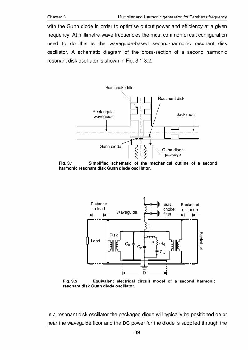
39
Chapter 3 Multiplier and Harmonic generation for Terahertz frequency
with the Gunn diode in order to optimise output power and efficiency at a given
frequency. At millimetre-wave frequencies the most common circuit configuration
used to do this is the waveguide-based second-harmonic resonant disk
oscillator. A schematic diagram of the cross-section of a second harmonic
resonant disk oscillator is shown in Fig. 3.1-3.2.
In a resonant disk oscillator the packaged diode will typically be positioned on or
near the waveguide floor and the DC power for the diode is supplied through the
Load
Backshort
Bias choke filter
LP
Disk
Waveguide
CG
-RG CP
LB CD
D
Backshort distance
Distance to load
Fig. 3.2 Equivalent electrical circuit model of a second harmonic resonant disk Gunn diode oscillator.
Rectangular waveguide Backshort
Resonant disk
Bias choke filter
Gunn diode package
Gunn diode
Fig. 3.1 Simplified schematic of the mechanical outline of a second
harmonic resonant disk Gunn diode oscillator.

40
Chapter 3 Multiplier and Harmonic generation for Terahertz frequency
bias post and choke assembly (often a single piece of machined metal), which is
insulated from the waveguide block. The operational principle is such that three
distinct electromagnetic modes of propagation exist [12, 49]: a TE01 rectangular
waveguide mode (in the rectangular waveguide section) at second harmonic
frequency, a radial mode (between the resonant disk and the waveguide floor),
and a quasi-coaxial (quasi-TEM) mode (between the resonant disk and the
bottom of the choke). Operation is such that a fundamental frequency resonance
exists in the TEM (Transverse ElectroMagnetic) mode along the quasi-coaxial
line between the choke and the disk. The radial disk couples energy between the
magnetic fields of the radial mode and the TE01 waveguide mode at the second
harmonic frequency.
The equivalent electrical circuit for a second harmonic resonant disk oscillator is
given in Fig. 3.2. Here the Gunn diode itself is represented as a capacitance CG
and a negative resistance –RG, while package capacitance and bond wire
inductance are modelled as CP and LB respectively. The capacitance CD is
associated with the resonant disk while the inductance LP is that of the post.
Generally speaking, the impedances of the bias post, disk and cavity are much
greater than those associated with the packaged diode. The frequency of
oscillation is therefore determined mainly by a combination of the resonant disk
diameter, post width, and the length of the post between the resonant disk and
the bottom of the lowest choke section. It is however noted that as frequency is
increased, the impedance’s related to the packaged Gunn diode becomes
increasingly significant compared to those of the post, disk and cavity: it has
been shown (through measurement and simulation) that a small, controlled
change in bond ribbon profile can easily produce a frequency shift of around 800
MHz in a 77 GHz oscillator. In order to obtain maximum second harmonic power
at the output, the dimensions and position of the radial disk must be optimised
not only to obtain, in conjunction with the post geometry, a particular
fundamental frequency resonance in the quasi-coaxial region, but also to
maximise the coupling between the radial mode and the TE01 waveguide mode
at the second harmonic frequency. This coupling is also dependent on the
backshort position: it is noted that in practical oscillators, the coupling between
the radial mode and waveguide mode is detuned (decoupled) from the optimum
to reduce load pull effects. It is also noted that the fundamental frequency is

41
Chapter 3 Multiplier and Harmonic generation for Terahertz frequency
below the cut-off of the rectangular waveguide and so is confined to the quasi-
TEM region.
The Gunn diode operation and hot-electron injection, Gunn diode
electromagnetic modelling, interaction between the diode and oscillator circuit
and proposed modelling techniques are discussed below.
3.2.1 Gunn Diode Operation and Hot-Electron Injection
A brief description of Gunn diode and Gunn diode oscillator operation is included
here as this is required to adequately explain the non-trivial nature of accurate
oscillator simulation. The details including device physics are discussed in
chapters 4 and 5. The Gunn diode can, at its most basic, be thought of as a DC-
to-RF converter: when an applied bias voltage exceeds a certain threshold,
oscillation will occur, the free-running frequency of which will depend on the
material properties and the geometry of the device itself. This is due to the
transferred electron effect exhibited by certain binary and ternary compound
semiconductors.
As an electron is accelerated by an electric field through a transferred electron
effect supporting material, it accumulates energy and so the probability of it
being scattered (transferred) from the central conduction band valley to the
nearest (in terms of energy and momentum) satellite valley increases. This
probability increases dramatically when the electric field reaches a certain
threshold value related to the distance in energy and momentum, between the
conduction band’s central valley and the nearest satellite valley. The scattering
mechanism is columbic in nature and involves a change in both momentum and
energy and so the transfer process is extremely inefficient with large amounts of
energy being lost to phonon excitation (and consequent elevation of the lattice
temperature).
The transferred electron effect results in oscillation because the effective electron
mass (related to the parabolicity of the conduction band profile) is greater in the
satellite valley than in the central valley. This means electron velocity in the
satellite valley due to an applied electric field is lower than that in the central
valley. The effect of this is a ‘bunching’ of electrons as they travel along the

42
Chapter 3 Multiplier and Harmonic generation for Terahertz frequency
length of the device, with those in the satellite valley moving at a slower rate than
those in the central valley. This leads to a depleted region (of electrons) followed
by a region of accumulation (known collectively as a high-field domain), which
sets up an internal electric field opposing that applied externally. The effect of
this is a continuing reduction in the net electric field across the device which
continues until a certain threshold electric field is crossed (preventing the
nucleation of any further high-field domains). At this point the high-field domain
stops expanding and propagates at a constant velocity through the device until it
reaches the anode contact layer at which point it collapses and the electric field
through the device increases again. Oscillation is observed in the current and
voltage at the device terminals as the domain forms at the cathode, expands,
propagates and collapses at the anode, before another domain nucleates at the
cathode.
The oscillation frequency and RF output power level are therefore fundamentally
governed by a combination of the transit region length and carrier concentration:
these define the high-field domain’s transit time through the diode, and the size
(in the direction of the electric field gradient) of the high-field domain. However,
the maximum useable frequency of a transferred electron device is generally
limited by the inter conduction band energy relaxation time: the time constant
governing the return of an electron from the satellite valley to the central valley.
The fundamental physics behind conventional Gunn device operation are
therefore very much centred on electron energy, lattice temperature, and random
scattering processes. These give rise to the following inherent limitations of
conventional Gunn devices:
• The onset of oscillation (turn-on voltage) in a Gunn device varies greatly with
ambient temperature.
• The oscillation frequency is highly dependent on temperature as it is defined
(in part) by the length of the region in which the domain propagates (transit
region). A small portion (referred to as the ‘dead zone’) of this region is
required to accelerate electrons to the point at which they have sufficient
energy to transfer to the satellite valley. The length of the dead zone, and
43
Chapter 3 Multiplier and Harmonic generation for Terahertz frequency
therefore the effective transit region length and oscillating frequency are also
dependent on temperature.
• The random nature of the scattering mechanisms which facilitate domain
nucleation, lead to small variations in the point at which domain nucleation
occurs. This effectively varies the length of the transit region from cycle-to-
cycle leading to enhanced phase noise at the output.
In order to address these issues the use of a hot electron injection structure
based on a graded gap AlGaAs launcher was proposed and demonstrated in the
1980’s [12, 50, 51]. The reasoning behind this was to raise the electron energy
sufficiently to greatly increase the probability of their direct entry to the
conduction band satellite valley upon delivery to the transit region. The injected
electrons have greater energy than those at equilibrium with the transit region
lattice, and so are referred to as ‘hot’. With the majority of the injected electrons
directly entering the satellite valley, the dead-zone is effectively eliminated along
with the temperature dependency of the oscillation frequency and turn-on
voltage. In addition the overall conversion efficiency is increased (due to the
reduced parasitic positive resistance) and because the random factors of domain
nucleation are reduced, the phase noise is decreased.
3.2.2 Gunn Diode Electromagnetic Modelling
In order to accurately model the behaviour of a waveguide oscillator circuit, a full-
wave, 3D high-frequency electromagnetic solver, such as Ansoft (ANSYS®) High
Frequency Structure Simulator (HFSSTM), is required. To this end, numerous
HFSSTM models of different second harmonic resonant disk oscillators that
correspond to the oscillators used to obtain measured results have been
developed at e2v Technologies Plc. These are typically 3-port models with ports
at the output waveguide, the top end of the choke (to evaluate filtering
effectiveness at both fundamental and harmonic frequencies) and at the Gunn
diode location. The Gunn diode port is, as in [52-54], set up as a coaxial
transmission line (the effects of which are de-embedded post-process) to
accurately represent the radial mode in the region of the diode and the resonant
disk, and allow the impedance in the region of the diode to be evaluated.

44
Chapter 3 Multiplier and Harmonic generation for Terahertz frequency
Fig. 3.3a shows an ANSYS® High Frequency Structure Simulator (HFSSTM)
model and electric field plot of a second harmonic resonant disk oscillator
configuration using a circular waveguide contacting back short and frequency
tuning pin. Although not showing the resonance in the quasi-coaxial TEM mode
(the plot illustrates the electric field at second harmonic frequencies, not
fundamental), Fig. 3.3b shows power being coupled between the diode and the
waveguide output (left), and a degree of interaction between the resonant disk
and the waveguide floor. For future work it is proposed to use these models to
establish the diode embedding impedance at both fundamental and second
harmonic frequencies. This will enable equivalent lumped element circuits for the
fundamental and second harmonic resonators to be defined, which can then be
coupled with the SILVACOTM model for subsequent time-domain simulations
(chapter 9).
Oscillators were modelled and simulated at e2v to assess the performance of
resonant disk Gunn diode oscillators (Fig. 3.4). It was believed that a reduced-
height waveguide oscillator could be used to increase the output power obtained
from the current D-band oscillators. An initial design was outlined and finalized
for fabrication. Additionally, Quartz packages (Fig. 3.5b) were tested at e2v for
(a) (b)
Fig. 3.3 (a) Ansoft HFSSTM
model of a second harmonic resonant disk millimetre-wave oscillator with tuning pin and circular waveguide sliding backshort. (b) Simulated field electric field plot for the oscillator at second harmonic frequencies.

45
Chapter 3 Multiplier and Harmonic generation for Terahertz frequency
use at frequencies above 125 GHz allowing increased power and frequencies
than achieved with standard alumina packages (Fig. 3.5a). Power combining of
two GaAs Gunn oscillators was achieved at 62.5 GHz with 210 mW output (Fig.
3.5c). That was intended for use as a high-power source for a frequency
multiplier.
3.2.3 Accounting for Interaction between the Diode and Oscillator Circuit
Previous modelling efforts have been concentrated on electromagnetic (EM)
modelling of the oscillator using idealized approximations for the diode [12, 55-
57]. Most advanced diode modelling work typically used either a hydrodynamic
(c)
Fig. 3.5 Gunn diode packages developed at e2v (a) Standard Alumni Packages DA810xx Bias-tuned Oscillators (b) Quartz Package.(c) Power Combining
(a)
• 125GHz ± 400MHz • 20mW min. output power • Phase Noise <-75dBc/Hz at
100kHz offset • -40°C to +70°C
• 76.5GHz ± 400MHz • 40mW min. output power • Phase Noise <-80dBc/Hz at
100kHz offset • +10°C to
• 62.5GHz ± 200MHz
• 100 mW min. output power
• Phase Noise <-80dBc/Hz at 100kHz offset
• +10°C to +70°C
(b)
(a) (b)
Fig. 3.4 Ansoft HFSSTM
simulations of a reduced-height waveguide model developed at e2v (a) second harmonic resonant disk millimetre-wave oscillator (b)simulated field electric field plot.
46
Chapter 3 Multiplier and Harmonic generation for Terahertz frequency
based approach [9, 57, 58] or Monte Carlo simulation techniques [59-61]. A
novel approach is proposed here which will be the first time a semiconductor
device modelling technique has been combined with an accurate 3D
electromagnetic modelling tool to accurately compute the behaviour of a Gunn
diode mounted in an oscillator.
Work has been reported where efforts have either been concentrated on EM
modelling of the oscillator using idealised approximations for the diode, or
concentrated on modelling the diode with approximations used for the oscillator
circuit. Of the work reported on the EM modelling of second harmonic Gunn
diode oscillators (mainly using HFSSTM), either the impedance of the Gunn
device is estimated as a static value [52], or a non-linear harmonic balance
simulator has been used to estimate the reactance of the device mounted in an
equivalent circuit [54]. Although the latter [54] attempts to incorporate the effects
of the dynamic reactance of the device in the EM simulations, the device model
used in the harmonic balance simulation was an idealised spice model (i.e. not a
true semiconductor device modelling tool) as the research focussed mainly on
the optimisation and behaviour of wideband tuneable Gunn oscillators rather
than evaluating the performance of the Gunn device itself. However, the latter
[54], represents the most accurate modelling technique yet demonstrated,
predicting oscillation frequency to a few GHz and RF output power to within 20%.
The majority of the work that concentrated on modelling the diode itself, which
typically used either a hydrodynamic based approach [57] or Monte Carlo
simulation techniques [12, 55, 59-62], generally relies on estimated values for
the parameters of an approximate equivalent oscillator circuit. These
investigations centred on analysis of the behaviour and performance of the diode
in isolation rather than in conjunction with an accurately modelled equivalent
circuit: this is partly due to the difficulties in combining Monte Carlo simulation
results with external circuit models due to the solution noise generated by the
stochastic nature of the technique. The aim of the majority of previous work was
to enable a study of domain formation and to compare the performance of
different device variations, and not to enable accurate modelling of the Gunn
diode and associated oscillator as a whole.

47
Chapter 3 Multiplier and Harmonic generation for Terahertz frequency
3.2.4 Proposed Modelling Techniques
The oscillator circuit effectively determines the oscillation frequency and so in
turn affects both the dynamics of the high-field domain within the device’s transit
region and therefore the dynamic reactance of the device itself. Here, due to the
cycle of domain nucleation, growth, propagation and collapse during each
oscillation cycle, the device capacitance (itself partly dependent on the oscillator
circuit parameters) varies throughout the oscillation cycle. It is therefore not
accurate to simply extract a small-signal s-parameter model of the Gunn device
from the SILVACOTM model and use this in conjunction with the HFSSTM model
of the oscillator (i.e. terminate the diode port in the HFSSTM simulation with a
SILVACOTM generated s-parameter matrix). This would not enable the effects of
the oscillator circuit to be taken into account when computing a device’s time-
domain response.
As SILVACOTM has the ability to include the effects of an external circuit on a
simulated device through the definition of a lumped element circuit in which the
device can be embedded, the effects of the external circuit can be considered
during computation of device behaviour. The equivalent frequency-domain
behaviour of a second harmonic oscillator circuit can therefore be simulated
using HFSSTM at the fundamental oscillation frequency and the equivalent circuit
parameters at this frequency extracted: this can then be used to define a suitable
circuit model for inclusion in the SILVACOTM simulations. From simulation of the
same HFSSTM model at second harmonic frequencies, the values of the
equivalent circuit elements at this frequency can be extracted and used in a
lumped element equivalent circuit model to estimate the conversion efficiency to
second harmonic. This will allow estimation of the second harmonic output power
for a device mounted in the oscillator. This will ultimately enable the effects of
both variations in the semiconductor device and the oscillator geometry to be
evaluated simultaneously.
The HFSSTM models for second harmonic resonant disk oscillators described in
section 3.2 accurately represent the geometry and materials of the circuit

48
Chapter 3 Multiplier and Harmonic generation for Terahertz frequency
including the package reactance values. The Gunn diode itself is currently
modelled using conductive GaAs for the contact layers and launcher, and bulk
semi-insulating GaAs (representing the depletion region in the high-field domain)
for the transit region. From the resulting small-signal frequency-domain s-
parameter file, all equivalent circuit element values (with the exception of the
diode parameters CG and -RG) can be accurately extracted at both fundamental
and second harmonic frequencies. It is noted here that modelling the whole
transit region as dielectric (representing the depletion region of the high-field
domain) is an approximation: in reality the depletion region does not fill the whole
transit region, only a varying portion of it. The depletion region increases through
the oscillation cycle as the high-field domain grows until, depending on the length
and doping of the transit region, it reaches a constant value that traverses the
length of then transit region, or (for short transit region devices) potentially
continues to grow until it collapses at the anode. This will influence the shape of
the fundamental frequency waveform and therefore its harmonic content
meaning it will also affect the level of second harmonic power that can be
extracted by the resonant disk circuit.
As the frequency of operation increases, not only do the impedances related to
the packaged diode become increasingly significant in relation to those of the
circuit, but in the shorter (sub-micron) transit region lengths the required mean
spread in variation of device reactance over the oscillation cycle will also
increase. This is due to a smaller percentage of the cycle time being devoted to
the steady propagation of the high-field domain through the transit region (i.e.
more of the cycle time will be consumed by domain formation and collapse as
opposed to steady domain propagation through the device). It is currently
thought that neglecting this variation when simulating the EM model will not
significantly affect the behaviour of the EM model produced, so long as an
accurate approximation of the diode structure is made. To achieve this, the
micron-scale transit region will be modelled as a suitably conductive bulk GaAs
material with an embedded insulating layer representing the high-field domain.
The size and position of this layer, along with suitable material properties
(permittivity and loss factor) can be estimated from an initial, free-running
SILVACOTM simulation.
49
Chapter 3 Multiplier and Harmonic generation for Terahertz frequency
As the dynamic nature of the depletion region is not negligible when simulating
the EM behaviour of the oscillator circuit (leading to degradation in accuracy of
the model as a whole) the growth of the high-field domain will need to be
adequately represented within the EM model. A proposed technique to achieve
this is to approximate the continuous process of domain growth and propagation
in the HFSSTM model by treating it as a sequence of discrete stages, each with
an individual HFSSTM model in which the length and/or the position of the
dielectric region is altered. The size, position and material properties of the
depletion region would again be estimated from an initial SILVACOTM result. A
time-varying series of equivalent circuit parameters could then be extracted, and
using curve fitting, continuous functions approximated for each of the oscillator
circuit spice model parameters. Although initially seeming labour intensive, this
process could be simplified through exploitation of the parametric sweep
functionality of HFSSTM. Suitable code would then be written to update the
values of the equivalent spice circuit model used to represent the oscillator circuit
in the SILVACOTM time-domain simulations, as the oscillation cycle progresses.
This approach is proposed as future work while developing and designing high
power THz sources using multipliers.
3.3 Frequency Multipliers
Multipliers were designed at e2v and several key doubler components (DC bias
filter, output waveguide taper, and a broadband cross-waveguide coupler) were
modelled for output at 140 GHz. The approach allowed verifying the design at
relatively low frequency, before it could be scaled to higher frequencies.
The fabrication technique used for the multiplier split block waveguide circuit is
dictated by the smallest feature size (typically the reduced height waveguide
required for the broadband performance of the cross-waveguide coupler). Thin-
film production of quartz circuits was routinely carried out at e2v on 127 µm
substrates. It was thought that for prototyping and higher-frequencies, circuits
using thinner substrates could be fabricated using standard semiconductor
processing techniques.

50
Chapter 3 Multiplier and Harmonic generation for Terahertz frequency
The design methodology used to design multiplier is shown in Fig 3.6 and
discussed below:
• Based on the operational frequency and power requirements, a suitable
diode or diode array geometry is identified. The diode size and number of
anodes are determined.
• The diodes C-V, I-V and RF characteristics are measured. The SPICE
parameters (series resistance, series current, built-in potential, ideality factor,
and capacitance) are fitted to the measurements.
• Non-linear circuit analysis is performed using harmonic balance simulator
tool such as Microwave Office ® by AWR. The harmonic balance simulator
determines optimum diode embedding impedance, especially for resistive (real)
impedance component. It calculates maximum theoretical conversion efficiency
Non-linear circuit analysis
(Harmonic Balance using MWO®)
Linear electromagnetic structure simulations
(FEMTM
, HFSSTM
)
Diode Impedance Generalized n-port s-matrix
• Linear circuit simulations AWR Microwave Office (MWO®)
• Circuit tuning
• Input impedance
• Diode mount impedance
• Power balance between diodes
Fig. 3.6 Frequency multiplier design methodology developed at e2v showing both hydrodynamic and liner electromagnetic structure modelling.

51
Chapter 3 Multiplier and Harmonic generation for Terahertz frequency
and power. It can be used to study the effects of chip parasitics on maximum
theoretical efficiency.
• HFSSTM is used to create a model of the diode chip and the waveguide
circuit in which it is embedded. It enables impedance seen at the individual
anodes to be evaluated.
• Simulation and tuning of entire multiplier circuit.
Millimetre-wave frequency multiplication using Schottky diode technology design
methodology was extensively verified against published designs and data at e2v.
The harmonic balance simulation tool, Linear EM Structure Simulations and
Schottky diode Varactor are discussed;
3.3.1 Harmonic Balance Simulation Tool
A harmonic balance simulation tool was created using Microwave Office ® by
AWR (Fig. 3.7), specifically for analysis and prediction of GaAs Schottky diode
performance given device’s basic electrical characteristics. The extensive
comparison to published work at e2v allowed accurate prediction of maximum
conversion efficiency for a given device, under specified conditions. The tool is
fully parametric and can be used to study the effects of operating conditions etc.
on the final performance (Fig. 3.8), as well as calculating the optimum
embedding impedances in the multiplier circuit. The results of the harmonic
balance simulations can therefore be used along with electromagnetic simulators
to design and tune circuit parameters for optimal circuit performance. Other
circuit components such as input and output waveguide tapers, microstrip-to-
waveguide coupling structures, and hammerhead bias filters have all been
designed at e2v Technologies Plc. at frequencies up to 140 GHz.

52
Chapter 3 Multiplier and Harmonic generation for Terahertz frequency
Fig. 3.8 Result of a harmonic balance parametric sweep to study output power with variation in input embedding impedance (with other operating conditions fixed) PIN
= 21 mW at 100 GHz, FOUT = 200 GHz
Fig. 3.7 A harmonic balance simulation tool schematics created using Microwave Office ® by AWR, specifically for analysis and prediction of GaAs Schottky diode performance given device’s basic electrical characteristics.
INDID=L1L=lf pH
DCVSID=V1V=bias V
RealSweep=30ImSweep=50Cmmwave=2.24Cpp=0lf=10bias=3.7
ZinR=8 ZinIm=52ZoutR=13 ZoutIm=29ZinNorm=complex(ZinR, ZinIm)/50ZoutNorm=complex(ZoutR, ZoutIm)/50GammaN=(ZinNorm-1)/(ZinNorm+1)GammaOUT=(ZoutNorm-1)/(ZoutNorm+1)M1=abs(GammaN)A1=deg(angle(GammaN))M2=abs(GammaOUT)A2=deg(angle(GammaOUT))
Xo Xn. . .
SWPVARID=1VarName="ZoutR"Values=stepped(1, RealSweep, 1)UnitType=None
PORT1P=1Z=50 OhmPwr=14.5 dBm
1 2
3
CIRCID=U1R=50 OhmLOSS=0 dBISOL=1000 dB
PORTP=2Z=50 OhmPORT
P=3Z=50 Ohm
Xo Xn. . .
SWPVARID=2VarName="ZoutIm"Values=stepped(1, ImSweep, 1)UnitType=None
M_PROBEID=VP1
3:Bias
1 2
HBTUNER2ID=OutputTunerMag1=1Ang1=180 DegMag2=M2Ang2=A2 DegMag3=1Ang3=180 DegFo=100 GHzZo=50 Ohm
3:Bias
12
HBTUNER2ID=InputTunerMag1=M1Ang1=A1 DegMag2=1Ang2=180 DegMag3=1Ang3=180 DegFo=100 GHzZo=50 Ohm
CAPID=C2C=Cmmwave fF
CAPID=C1C=Cpp fF
SDIODEID=SD1
2040
6080
100
0
1
2
3
4
5
6
7
8
9
10
510
1520
2530
Outp
ut
Pow
er
(mW
)
Rin
Xin

53
Chapter 3 Multiplier and Harmonic generation for Terahertz frequency
3.3.2 Linear EM Structure Simulations
Other circuit components such as input and output waveguide tapers, microstrip-
to-waveguide coupling structures, and hammerhead bias filters have all been
designed at e2v Technologies Plc at frequencies up to 140 GHz. Initial designs
outlining the geometry of Schottky diode arrays suitable for use in frequency
doublers and triplers have been produced (Fig. 3.9).
HFSSTM was used to create a model of the diode chip and the waveguide circuit
in which it is embedded, which enables impedance seen at the individual anodes
to be evaluated (Fig. 3.9a). Varactor Chip Waveguide Mount Modelling (Fig.
3.9b) shows diode chip model embedded in a waveguide diode mount.
3.3.3 Semiconductor Component – Schottky Diode Varactor
The harmonic oscillations of the input signal created in the multiplier are
produced by a non-linear component, in this case a Schottky diode Varactor. In
order to achieve a low RC time constant, both the capacitance and series
resistance need to be kept as low as possible. In practice this is achieved by
using small area anodes for the lowest possible capacitance, and although this
(a)
(b)
Fig. 3.9 (a) Varactor Diode Chip and the waveguide circuit model created using HFSS
TM at e2v Technologies Plc (b) HFSS
TM diode chip model embedded in waveguide diode
mount.

54
Chapter 3 Multiplier and Harmonic generation for Terahertz frequency
does increase the series resistance, the overall effect is still to reduce the RC
time constant in properly designed structures. The challenge is then to reduce
the series resistance as much as possible for a specific Schottky contact.
The device structure shown in Fig. 3.10 consists of a traditional GaAs diode
structure topped by a heavily doped region of InxGa1-xAs graded from x=0 at the
GaAs interface to x=0.53 at the upper surface. A subsequent heavily doped layer
was grown to form the low resistance non-alloyed Ti/Au Ohmic contact. The
fabrication process was such that the metallisation layer used to form the Ohmic
contact was also utilised to provide the Schottky contact, after the appropriate
patterned wet recess etch though the InGaAs layers to the GaAs. A
methane/hydrogen RIE (Reactive Ion Etching) step was then used to etch
through the lightly doped GaAs layer to the highly doped conductive region
below (conventionally the Ohmic contact layer with alloyed contacts). Importantly
the contact metals are used as an etch mask. An air bridge (2 µm wide) was then
formed between the anode and a bond pad to complete the device.
Titanium 0.04um + Gold 0.5µm
Substrate GaAs 1x016 cm-3 8µm
Buffer GaAs undoped 0.05µm
Etch Stop AlAs undoped 0.08µm
Membrane GaAs 1x1016 cm-3 3µm
N+ GaAs 5x1018 cm-3 3µm
Contact (n) GaAs 1.8x1017 cm-3 0.35µm
Graded InGaAs In 53% to 0% 5x1018 cm-3 0.0605µm
Ohmic n++ InGaAs In 53% 5x1018 cm-3 0.033µm
100µm
106µm
2µm
Tn+Au
Schottky
4µm
Cathode
Anode
Fig. 3.10 2D GaAs diode structure topped by a heavily doped region of InxGa1-xAs graded from x=0 at the GaAs interface to x=0.53 at the upper surface.
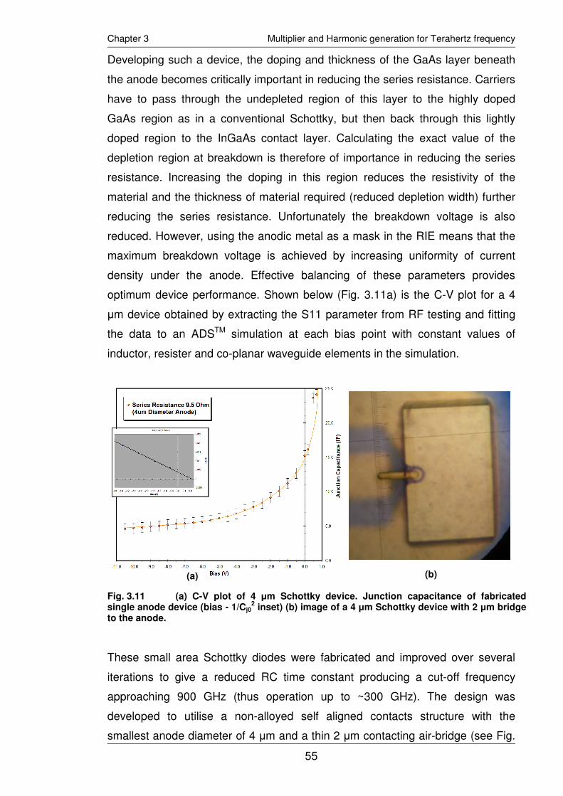
55
Chapter 3 Multiplier and Harmonic generation for Terahertz frequency
Developing such a device, the doping and thickness of the GaAs layer beneath
the anode becomes critically important in reducing the series resistance. Carriers
have to pass through the undepleted region of this layer to the highly doped
GaAs region as in a conventional Schottky, but then back through this lightly
doped region to the InGaAs contact layer. Calculating the exact value of the
depletion region at breakdown is therefore of importance in reducing the series
resistance. Increasing the doping in this region reduces the resistivity of the
material and the thickness of material required (reduced depletion width) further
reducing the series resistance. Unfortunately the breakdown voltage is also
reduced. However, using the anodic metal as a mask in the RIE means that the
maximum breakdown voltage is achieved by increasing uniformity of current
density under the anode. Effective balancing of these parameters provides
optimum device performance. Shown below (Fig. 3.11a) is the C-V plot for a 4
µm device obtained by extracting the S11 parameter from RF testing and fitting
the data to an ADSTM simulation at each bias point with constant values of
inductor, resister and co-planar waveguide elements in the simulation.
These small area Schottky diodes were fabricated and improved over several
iterations to give a reduced RC time constant producing a cut-off frequency
approaching 900 GHz (thus operation up to ~300 GHz). The design was
developed to utilise a non-alloyed self aligned contacts structure with the
smallest anode diameter of 4 µm and a thin 2 µm contacting air-bridge (see Fig.
(b)
Fig. 3.11 (a) C-V plot of 4 µm Schottky device. Junction capacitance of fabricated single anode device (bias - 1/Cj0
2 inset) (b) image of a 4 µm Schottky device with 2 µm bridge
to the anode.
(a)

56
Chapter 3 Multiplier and Harmonic generation for Terahertz frequency
3.11b). It produced low contact resistance and capacitance with a still relatively
high breakdown voltage. That material was decided to be used to fabricate
smaller anode devices for reduced RC time constant and higher frequency
operation.
At the University of Manchester new process techniques were developed for
undercut air bridges to reduce device parasitics, process complexity and series
resistance. Yield and uniformity was increased in order to repeatedly deliver the
more complicated multiple device anti-series structures required and thick (> 2.5
µm) lift-off processes were developed. Those processes allowed the design of
new devices in collaboration with multiplier design requirements across a wide
range of chip size and device combination totalling over 700 individual device
structures (such as Fig. 3.12). Junction capacitance was extracted from RF
testing indicating 4.8 fF at breakdown (Fig. 3.11). These devices gave a
theoretical cut-off frequency in excess of 1.1 THz.
3.4 Schottky Diode SILVACOTM Modelling
A Schottky diode 2D model has been developed in SILVACOTM. Its epitaxial
structure is shown in Fig. 3.13. The conduction band diagram of both ohmic and
Schottky contacts are shown in Fig. 3.13b and 3.13c. The models and material
parameters are given in Appendix 2.
(b) (a)
Fig. 3.12 Six anode anti-series device single anode (full circuit inset) (a) design (b) fabricated device.

57
Chapter 3 Multiplier and Harmonic generation for Terahertz frequency
The modelled versus measured results matched very well (Fig 3.14 - 3.16). The
Schottky contact breakdown voltage analysis is shown in Fig. 3.14. The model
Fig. 3.14 Forward bias I-V curve for a 4 µm diameter anode Schottky diode.
Series resistance sR
was calculated from curve’s slope.
0.0 0.1 0.2 0.3 0.4 0.5 0.6 0.7 0.8 0.90
10
20
30
40
50
60
70
80
90
100
110
120
Modelled fwd current Measured fwd current
Anode C
urr
ent (u
A)
Voltage (V)
Titanium 0.04um + Gold 0.5µm
N+ GaAs 5x1018 cm-3 3µm
Contact (n) GaAs 1.8x1017 cm-3 0.35µm
Graded InGaAs In 53% to 0% 5x1018 cm-3 0.0605µm
Ohmic n++ InGaAs In 53% 5x1018 cm-3 0.033µm
50µm
54µm
2µm
Tn+Au
2µm
SchottkyC
ond
uction b
and e
nerg
y (
eV
)
Cond
uction b
and e
nerg
y
(eV
)
SILVACO Anode Schottky contact Conduction band diagram at 0V SILVACO Cathode graded
InGaAs ohmic contact Conduction band diagram at 0V
Device width µm Device width µm
Cond
uction B
an
d
Cond
uction B
an
d
Fig. 3.13 GaAs Schottky diode SILVACOTM
2D model. Equal area rule was maintained same as the manufactured device (a) 2D device structure for a 4 µm diameter anode Schottky diode (b) Conduction band diagram for GaAs Schottky contact (c). Conduction band diagram at zero bias showing graded InGaAs ohmic contacts

58
Chapter 3 Multiplier and Harmonic generation for Terahertz frequency
gives a series resistance of 6 Ohms, substantially less than the measured value
of 9.5 Ohms. This is attributed to external device resistances and modelled
device rectangular geometry. The model can be used to study underlying device
physics and extract parameters such as ideality factor, zero voltage junction
capacitance, built in voltage and breakdown voltage. These parameters will be
used in harmonic balance simulations created using Microwave Office ® by
AWR, which will allow analysing and prediction of the GaAs Schottky diode
performance at mm-wave frequencies.
The modelled Schottky diode capacitance-voltage (C-V) plot matched very well
with measured data (Fig. 3.15). The junction capacitance indicated 4.6 fF at
breakdown and a Cjo of ~17 fF giving a theoretical cut-off frequency in excess of
1.1 THz.
Three Schottky models listed in table 3.1 were developed and compared with
measured results (Fig. 3.16). They were designed in collaboration with multiplier
design requirements for ~120 GHz output. An additional area was included in
modelled devices that were in line with fabricated devices. The C-V plots were
compared with measured results and junction capacitance Cj0 was determined.
The cut-off frequencies were calculated as shown in table 3.1
Fig. 3.15 C-V plot for a 4 µm diameter anode Schottky diode
-11 -10 -9 -8 -7 -6 -5 -4 -3 -2 -1 02
3
4
5
6
7
8
9
10
11
12
13
14
15
16
17
18
Modelled Capacitance Measured Capacitance
Ca
pacitance (
fF)
Voltage (V)
Anode diameter 4um
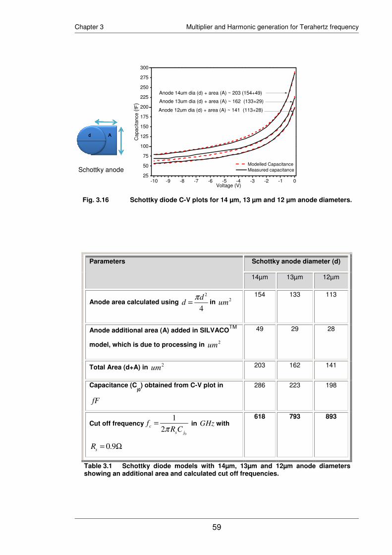
59
Chapter 3 Multiplier and Harmonic generation for Terahertz frequency
Parameters Schottky anode diameter (d)
14µm 13µm 12µm
Anode area calculated using
2
4
dd
π= in 2
um 154 133 113
Anode additional area (A) added in SILVACOTM
model, which is due to processing in 2um
49 29 28
Total Area (d+A) in 2um 203 162 141
Capacitance (Cj0) obtained from C-V plot in
fF
286 223 198
Cut off frequency
0
1
2c
s j
fR Cπ
= in GHz with
0.9s
R = Ω
618 793 893
Table 3.1 Schottky diode models with 14µm, 13µm and 12µm anode diameters showing an additional area and calculated cut off frequencies.
-10 -9 -8 -7 -6 -5 -4 -3 -2 -1 025
50
75
100
125
150
175
200
225
250
275
300
Capacitance (
fF)
Voltage (V)
Modelled Capacitance
Measured capacitance
Anode 14um dia (d) + area (A) ~ 203 (154+49)
Anode 13um dia (d) + area (A) ~ 162 (133+29)
Anode 12um dia (d) + area (A) ~ 141 (113+28)
Fig. 3.16 Schottky diode C-V plots for 14 µm, 13 µm and 12 µm anode diameters.
Schottky anode

60
Chapter 3 Multiplier and Harmonic generation for Terahertz frequency
3.5 Conclusion
The Gunn diode operation and hot-electron injection, Gunn diode
electromagnetic modelling, interaction between the diode and oscillator circuit
and proposed modelling techniques were discussed. Two novel modelling
techniques to merge SILVACOTM and HFSSTM models and to account for
interaction between the Gunn diode and oscillator circuit were presented. The
techniques include the lumped element model for SILVACOTM and taking into
account Gunn diode domain growth and propagation in the HFSSTM model
Multipliers designed at e2v and several key doubler components (DC bias filter,
output waveguide taper, and a broadband cross-waveguide coupler) modelled
for output at 140 GHz have been presented in detail. Oscillator cavity developed
in HFSSTM and harmonic balance simulation tool created in Microwave Office ®
by AWR at e2v Technologies Plc. were discussed. The harmonic balance
simulation tool, Linear EM Structure Simulations and Schottky diode Varactor
were presented.
Both semiconductor components of the multiplier namely the Gunn diode and the
Schottky diode have been presented. It was shown that the modelled Schottky
diode C-V plot matched very well with measured data. The junction capacitance
indicated 4.6 fF at breakdown and a Cjo of ~17 fF giving a theoretical cut-off
frequency in excess of 1.1 THz. Additionally, three Schottky models, designed in
collaboration with multiplier design requirements for ~120 GHz output, were also
compared with measured results. An additional area was included in modelled
devices that were in line with fabricated devices. The C-V plots were compared
with measured results and junction capacitance Cj0 was determined. The cut-off
frequencies were shown.

Chapter 4 Gunn Diode Theory
4.1 Introduction
The Gunn Diode, named after J. B. Gunn, who discovered the Gunn Effect, is an
active solid state two terminal device, classed as Transferred Electron Device
(TED). The most conspicuous feature of the device is the negative differential
resistance, which depends on the bulk material properties [28]. In this chapter
after covering the basic Gunn diode theory, the negative differential resistance
phenomenon will be analyzed with relation to material band structure. Finally the
various device operating modes will be discussed with emphasis on the high
frequency oscillations before summarizing the limitations of conventional Gunn
diodes.
4.2 Gunn Diode as Transferred Electron Effect (TED) Device
The Gunn diode can, at its most basic, be thought of as a DC-to-RF converter:
when an applied bias voltage exceeds a certain threshold, voltage oscillation will
occur, the free-running frequency of which will depend on the material properties
and the geometry of the device itself. This is due to the transferred electron effect
exhibited by certain binary and ternary compound semiconductors. The
transferred electron effect is reviewed in detail through Electric Field Effects on
Electron Drift Velocity, High Field Transport in n-GaAs, Negative Differential
Resistance (NDR) and Conditions for Negative Differential Mobility.
4.2.1 Electric Field Effects on Electron Drift Velocity
At low electric-fields the electron drift velocity is linearly proportional to the
applied electric field. However, it departs from the linear relationship with the
increase in applied electric-field, which causes the drift velocity to approach the
thermal velocity value. Before considering the high electric field effects the
61

62
Chapter 4 Gunn Diode Theory
following gives a brief account covering the essentials of low field electron drift
velocity and its corresponding high field effects [3].
The low field electron drift velocity is given as:
ετ
−=
n
cn m
qv cm/s ………………….…………..……………..(4.1)
where nv is electron drift velocity, ε is the applied electric field, cτ is the mean
free time and nm is the effective electron mass. The drift velocity is proportional
to the electric field and the proportionality factor is known as the mobility, which
is given by:
n
c
nm
qu
τ= ………………………………………………………….. (4.2)
Thus the drift velocity can be written as:
εnn uv −= ………………………….……..……………………..... (4.3)
where the negative sign indicates that the electrons move in the opposite
direction to the applied electric field. The mobility determines the influence of
electric field on the motion of an electron. At low electric-field values the drift
velocity of electrons is linearly proportional to the applied electric field and is
smaller than the thermal carrier velocity (which is scm /107.7 6× [1] for n-type
GaAs). As the electron drift velocity approaches the thermal velocity, the linear
relationship due to the corresponding constant mobility breaks down. The drift
velocity increases with the increase in electric field until reaching a saturation
velocity value. The plots of carrier drift velocity versus electric field for Gallium
Arsenide (GaAs), Indium Phosphide (InP) and Gallium Nitride (GaN) are shown
in Fig. 4.1, where it can be seen that the drift velocity after reaching a maximum
value decreases with an increase in applied field.
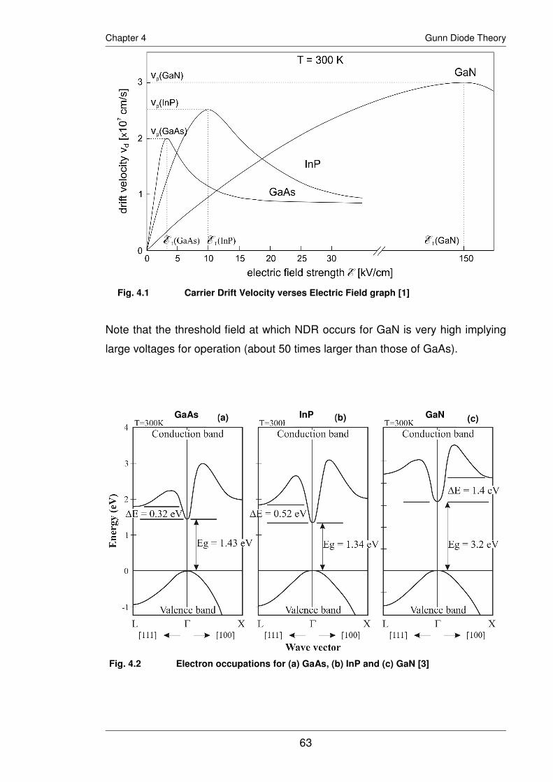
63
Chapter 4 Gunn Diode Theory
Note that the threshold field at which NDR occurs for GaN is very high implying
large voltages for operation (about 50 times larger than those of GaAs).
(a) (b) (c) GaAs InP GaN
Fig. 4.2 Electron occupations for (a) GaAs, (b) InP and (c) GaN [3]
Fig. 4.1 Carrier Drift Velocity verses Electric Field graph [1]

64
Chapter 4 Gunn Diode Theory
4.2.2 High Field Transport in n-GaAs
The negative differential mobility phenomenon can be explained through
consideration of the band diagrams shown in Fig. 4.2. Fig. 4.2a shows that GaAs
is a direct band gap material with an energy gap, between the top of valence
band and bottom of conduction band, of 1.43 eV at k=0 (zero wave vector). The
satellite conduction band minimum (L) is 0.32 eV higher than the conduction
band minimum (Γ) and is at 2 /k aπ= ± (where a is the lattice constant). At 300K,
n-type GaAs has its valence band highly occupied with few electrons in the
conduction minimum (central Γ band) and nil in the satellite L band. However, as
the increase in applied electric field reaches ~3kV/cm, some electrons from the
Γ valley gain sufficient energy and are scattered into the L valley.
As shown by equation 4.2, electron mobility is dependent on effective electron
mass, which is different in the different conduction band valleys and depends on
the local curvature of the band structure. The effective electron mass is given by
[29]:
∂
∂=∗
2
2
22
1
1
k
Em
…………...……………………….………………(4.4)
Where ∗m is the effective mass, π2/h= is planks constant and k is the wave
vector. In the satellite valley the curvature is higher than the central valley, which
results in a higher effective mass compared to the central Γ valley. For GaAs,
electrons have an effective mass of 04.0 m (∗
1m ) in the L valley and 0068.0 m (∗
2m )
in the Γ valley [2].
The density of states of each Γ and L valley represent a number which is
proportional to energy interval available to the conduction electrons and number
of allowed energy states per unit volume. Its ratio, R, is given by:
2
3
1
2
1
2
=
∗
∗
m
m
M
MR ……………………………..……………………….(4.5)

65
Chapter 4 Gunn Diode Theory
Where 1M and
2M are the equivalent Γ and L valley whose values for GaAs
are 1 and 4 respectively [34]. Thus the density of states ratio becomes R=94 [34,
63], which is much higher than the corresponding Γ valley. In the L valley in
addition to the higher electron effective mass, the electrons are also subjected to
stronger scattering processes [64]. These effects collectively result in lower
electron mobility (up to 70 times) in the L valley compared to the Γ valley.
4.2.3 Negative Differential Resistance (NDR)
In Fig. 4.3a applied electric-field is low ( aεε < ) thus all the electrons are in the
central valley. As the field is increased ( ba εεε << ) some electrons gain the
energy required to transfer to upper valley as shown in Fig. 4.3b. Finally when
the field is large enough ( bεε > ) effectively all the electrons are transferred to
the upper valley. The effect of this on the drift velocity is shown in Fig. 4.4, which
can be equated as [3]:
ε1uvn ≅ when aεε <<0 ……….………………….………………(4.6)
ε2uvn ≅ when bεε > …………….…………………………….….(4.7)
(a) (b) (c)
aεε < ba εεε << bεε >
Fig. 4.3 Electron occupations under various Electric Field levels for n-GaAs [3]

66
Chapter 4 Gunn Diode Theory
The electron drift velocity increases linearly until the onset of negative differential
resistance where the electric filed value is given as aε . The drift velocity
continues to decrease until the field acquires the maximum value bε as shown in
Fig. 4.4.
It can be seen from Fig. 4.4 that au ε1 is greater than bu ε1 , which results in a
decrease of drift velocity between aε and bε , The NDR exists between the
threshold field (Tε ) and final valley field ( Vε ) as shown in Fig. 4.4 [1, 3].
If the electron mobility, effective mass and density for both central (Γ band) and
satellite (L band) valleys are denoted by 111 ,, nmu and
222 ,, nmu respectively then
the steady state conductivity of n-type GaAs is given as [3]:
uqnnunuq =+= )( 2211σ ………………………………....…………(4.8)
Where u is the average mobility and is given by:
)(
)(
21
2211
nn
nunuu
+
+= ………………………………………….…………(4.9)
ε1qnu
ε2qnu
Electric Field KV/cm
Carr
ier
Drift
Velo
city
cm
/s
Fig. 4.4 Negative Differential Resistance region [3]

67
Chapter 4 Gunn Diode Theory
Thus the average drift velocity can be written as:
εuvn = ……………………………………….……….……………(4.10)
4.2.4 Conditions for Negative Differential Mobility
For a material to exhibit the transferred electron effect and therefore negative
differential mobility, it must display the following characteristics [65]:
• The material satellite or L band energy minimum is above the normal
conduction band (Γ ) minimum.
• The E verses k curvature for L band is less than the Γ band minimum,
thereby providing greater effective mass values.
• The density of states in L band has a higher value than the Γ conduction
band.
• The energy gap between Γ and L valley must be greater than kT to avoid
occupation of L valley due to thermal occupations at low electric field: This
ensures that the occupation of L band is due to the applied electric-field.
• The fundamental energy gap, gE , must be greater than E∆ to avoid impact
ionization of electrons across gE before inter-valley transfer occurs.
• Some mechanism must be present to supply the k-value (momentum) change
required for transition to the satellite valley.
Besides GaAs materials such as InP and GaN depict the above characteristics
and thus are the favoured materials choices for the implementation of
Transferred Electron Devices (TED) [1, 3, 66].
4.3 Instability and Domain Formation
Semiconductors such as GaAs and InP, which exhibit the Transferred Electron
Effect are inherently unstable. The instability is due to the formation of a space

68
Chapter 4 Gunn Diode Theory
charge region that grows exponentially with time due to a small, random change
in carrier density in the semiconductor. This instability has been explained in [2],
and is discussed below:
In a uniformly doped semiconductor device with an electron concentration DN , a
noise process or variation of doping level or some crystal defects can cause a
spontaneous fluctuation in the electron density ( N ). This spontaneous
fluctuation forms a dipole, consisting of an accumulation and a depletion region
with associated electric field gradient. The non-uniformity in the space charge is
related to the electric field by the following Poisson equation:
xNNq rD
∂
∂=−
εεε 0)( ………………………………………………(4.11)
where 0ε and rε are the vacuum and relative permittivity respectively, and
DN is
the doping density. If the mean electric field is less than the threshold field then
electrons subjected to a higher electric field will move faster than those in the
low-field region. The space charge would then fill the depletion region resulting in
the dampening of the fluctuation due to dielectric relaxation.
Now considering the case when the applied electric field is greater than the
threshold electric field Tε : the electron drift velocity reduces in the region of
higher field, causing the space charge fluctuation to grow along with time
associated local electric field in the region as shown in Fig. 4.5b. This
exponential growth of electric field continues until a stable domain is formed as
shown in Fig. 4.5c. Stability arises because to keep the total voltage drop across
the device the same, the electric field outside the domain remains below the
threshold level. It can be seen in Fig. 4.5c that the electric field within the domain
reaches a peak value Pε , while outside the domain the electric field (
Rε ) is less
than the threshold value. Rε is therefore less than
Tε removing the drift velocity
difference (which causes the space charge to grow) and a stable domain is
formed. Additionally this means that when the domain is stable another domain
does not grow as Rε remains below
Tε .

69
Chapter 4 Gunn Diode Theory
4.3.1 Domain Dynamics
Once stable, the domain drifts through the device at a constant velocity. The
electric field is less than the threshold level outside the domain. The electric field
is at its peak at the outside edge of the accumulation region, where it is above
the threshold value. It drops across the domain until it becomes less than the
threshold field (at the outer edge of the depletion region). Butcher [58] has done
a detailed analysis of domain formation, which concluded that if the diffusion
parameter D is assumed constant and independent of electric field, then the
electron velocity outside domain, Rv , is the same as the domain drift velocity,
Dv .
Secondly Pε and
Rv are related by the dynamic characteristic. The dynamic
characteristic curve is related to velocity electric field ( v ε− ) curve by equal area
rule shown in Fig. 4.6 [1]. Using these results Hobson explained the current
conduction process within the domain as [2]:
0( )R r
NJ qNv qD
t x
εε ε ε
∂ ∂= + −
∂ ∂ …………………….……….……(4.12)
where, the current density J is constant throughout the device, and the three
terms represent, drift, displacement and diffusion components respectively.
Outside the domain both N and ε are independent of position thus the current is
N N N
ε ε ε
Pε
Rε
Bε
Tε
(a) (b) (c) Cathode Anode
DN
Cathode Anode Cathode Anode
Stable Domain
Fig. 4.5 Stable dipole domain formation with the growth of space-charge [2]

70
Chapter 4 Gunn Diode Theory
carried as conduction current and current density is due to the drift component
( )R
qNv ε . Within the domain all three components play roles due to the gradient
in both doping density ( N ) and ε . The change in electric field gradient causes a
displacement current to flow. At the peak electric field, Pε , value no
displacement current flows because 0=∂
∂x
ε . However, at Pε an electron
density gradient causes a diffusion current to flow. Thus in the depletion region,
the current is due to the displacement current while in the accumulation region
the current is due to the large conduction (drift) current, which is opposed by the
displacement and diffusion currents [4].
Conduction current
Diffusion current
Equal areas
Ele
ctr
on
dri
ft v
elo
city
Electric field (E KV/cm)
Dynamiccharacteristic curve
Rε
Pε
Rv
Vv
Vε
Tε
Fig. 4.6 Dynamic characteristics curve and electron drift velocity – electric field curve. It is plotted in SILVACO using MOCASIM (Monte Carlo simulator) for
GaAs 1.1x10⁻¹⁶
doped. Equal area relationship between Pε and
Rv is shown.
∞
Ele
ctric
Fie
ld
Acc
um
ula
tion R
egio
n
Tε
Rε
(a) (b) Cathode Anode Cathode Anode
Ele
ctro
n D
ensity
Fig. 4.7 Zero Diffusion Domain profiles [5]

71
Chapter 4 Gunn Diode Theory
Finally, if the diffusion current is neglected i.e. diffusion coefficient D is zero, then
the domain travels at the same velocity ( Dv ) as the electrons outside the domain
(Rv ). The electron density is zero in the depletion region and maximum ( ∞ ) at
the accumulation region. Thus a triangular shaped electric field is formed within
the domain, while outside domain the carrier concentration remains unchanged
at DN as shown in Fig. 4.7. The current density outside the domain is given as
RDqvNJ =∗ ………………………...………………...……………(4.13)
while inside the domain due to fully depleted region the current density is given
as
0 0r r DJ vt x
ε εε ε ε ε
∂ ∂= = −
∂ ∂ ……………………………..………….(4.14)
where Dv is the domain velocity. Poisson’s equation requires that
qNx
Dr −=∂
∂εεε 0
………………………………...…………………(4.15)
Thus the current density is given as
DD qvNJ = …………………………………………...…………….(4.16)
whereas outside the domain at 0=∂
∂x
ε and carrier density DNN = , using the
current continuity equation
DR vv = ……………………………….………………………….....(4.17)
the current is given as
RD vqNJ = …………………………….……………………………(4.18)

72
Chapter 4 Gunn Diode Theory
4.3.2 Device Oscillating Frequency
Generally in GaAs Dv is scm /101~ 7× for moderately doped material. As the
domain grows the current in an external circuit falls due to the fall in the field
outside the domain. As the domain reaches the anode, the electric field gradient
becomes zero and the domain collapses. The external electric field and current
values increase until reaching the threshold value and allowing another domain
to form at the cathode. The external current therefore oscillates at a frequency,
which is inversely proportional to the transit length tl (the distance between the
domain formation point and anode). The oscillating frequency can therefore be
given as:
t
D
l
vf =0 ……..………………………….…….…………………….(4.19)
Maximum operating frequency is determined by the material’s inter-valley energy
relaxation time. The electrons transfer from the Γ -valley to the L-valley and vice
versa in a finite time. At high frequencies ~60 GHz the energy relaxation time is
~3×10-12 sec [2], which has a significant effect on energy relaxation time and as
a result the RF cycle does not follow the ε−v curve. The NDR is reduced since
the current cannot rise as the electric field falls thus reducing the device
efficiency and power [5].
4.3.3 The Doping – Length (NDL) Product
Domain formation takes a finite time and distance and so to achieve stability
requires a minimum device length l for a given doping density DN . To determine
the minimum device length, it is compared with the domain length under applied
electric field. For a fully depleted triangular domain with width w , peak electric
field pε and external field Rε (as shown in Fig. 4.7b), the domain potential
Dφ is
given as:
2)(
wRpD εεφ −= ……..………………….…………………………(4.20)

73
Chapter 4 Gunn Diode Theory
From Poisson’s equation
D
Rpr
qNw
)(0 εεεε −= ……………………………….…………………(4.21)
And so solving equations 4.20 and 4.21, the domain potential becomes;
r
D
D
Rpr
D
wqN
qN εε
εεεεφ
0
22
0
22
)(=
−= ……………………..……………(4.22)
The ratio of peak to valley current is ~2 in GaAs, a threshold field twice as high
as the electric field outside the domain. Mathematically the domain potential is
given as;
2
T
D
wεφ = ……………………………………………..…………….(4.23)
Thus it can be stated that
12 20 2.4 10r TD
N l cmq
ε ε ε −> = × ……………………….……………(4.24)
4.3.4 Stable Operating Point of Domain
After analyzing the domain potential, the stable value of the outside field Rε with
regard to the applied voltage can be determined. If tl is the device length, w the
width, Dφ the domain potential and
BV the external bias voltage, then while
maintaining the electrical boundary condition, the external bias voltage, BV , is
given as:
)( wlV tRDB −+= εφ ………………………………..……………(4.25)
As domain length is very small ( tlw <<< ) it can be neglected and the bias
voltage given as:
tRDB lV εφ += ……………………………………...………………(4.26)

74
Chapter 4 Gunn Diode Theory
The minimum electric field value outside the domain required to sustain the
domain is shown in Fig. 4.8, where for a constant voltage BV , the domain
potential Dφ is plotted against the minimum electric field
Rε . The three load lines
correspond to three different terminal bias voltages (BV ). The intercepts are for a
given doping density, DN , and device length, tl . Therefore, the following three
configurations are possible [2, 29]:
• The average electric field, tB lV / , is greater than the threshold field yielding
the load line 1, which intersects at a point higher than Tε on the x axis. In this
condition only one stable solution is possible.
• The average electric field tB lV / is greater than the sustaining voltage
StS lV ε=/ but less that the threshold field (giving load line 2). For tB lV / less
than Tε , two solutions are possible. The first intersection point of the
Dφ - Rε
curve and load line gives a stable operating point. It can be seen that for a
steep load line i.e. a long device, the stable operating point is approximately
half the threshold value. Therefore, as shown earlier in equation 4.26, the
Stable
Unstable
Dφ
Rε Tε
Load Lines
1
2
3
Sε
Do
ma
in P
ote
ntial
Electric Field
Fig. 4.8 The domain potential Dφ and minimum electric field
Rε
(solid line) relationship due to the space-charge dynamics [2]

75
Chapter 4 Gunn Diode Theory
domain will sustain and continue to propagate even if the external voltage
drops below the threshold voltage. The unstable intersection is explained
through consideration of a small noise fluctuation, which causes Dφ to
increase, thus decreasing Rε . A decrease in the value of
Rε shifts the state
higher than the Dφ -
Rε curve. It shows that outside the domain the electrons
are moving faster than those inside the domain. It will cause the accumulation
and depletion regions to grow to keep the Poisson’s equation satisfied,
resulting in a further increase in Dφ . Eventually it will reach steady state and
the stable point on the load line will be achieved.
• The average electric field tB lV / is equal to the sustaining voltage StS lV ε=/
which gives line 3. This condition causes the domain to terminate while still
growing, with tB lV / greater than or less than the sustaining voltage. At the
sustaining voltage the load line is tangent to the Dφ -
Rε curve. Thus SV is
considered very important for the domain to grow and be sustained.
4.4 Conventional Gunn Diode
The Gun diode in its basic form is a homogenous device with ohmic contacts at
each end. The device has a sandwiched structure and comprises of +n contact
layers at the ends with a −n transit region in between, as shown in Fig. 4.9.
Do
pin
g C
on
ce
ntr
atio
n
De
ad
Zon
e
Co
nta
ct
Laye
r
−n Transit Region Length tl
Device Depth
Co
nta
ct
Laye
r
Effective Transit Length '
tl
+n
+n
Fig. 4.9 Conventional Gunn Diode structure
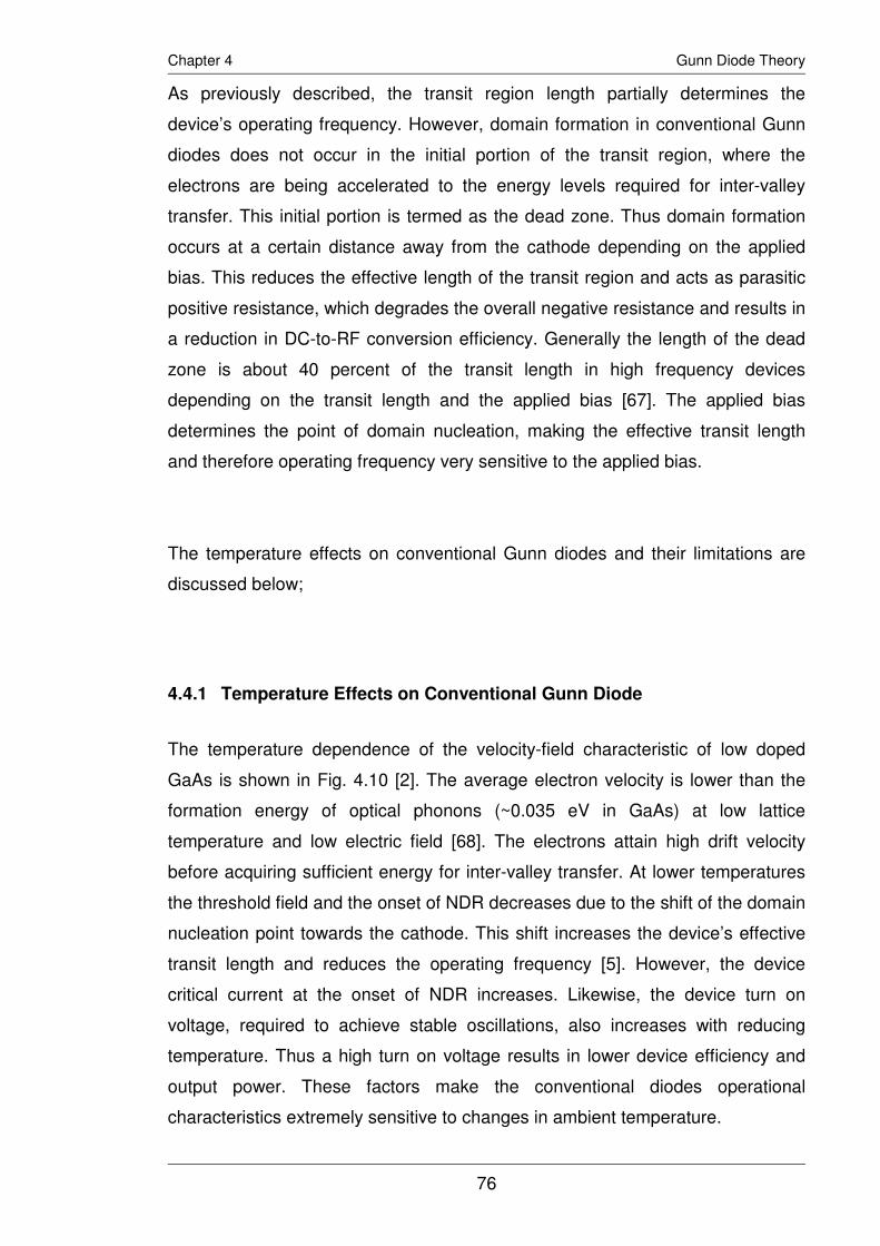
76
Chapter 4 Gunn Diode Theory
As previously described, the transit region length partially determines the
device’s operating frequency. However, domain formation in conventional Gunn
diodes does not occur in the initial portion of the transit region, where the
electrons are being accelerated to the energy levels required for inter-valley
transfer. This initial portion is termed as the dead zone. Thus domain formation
occurs at a certain distance away from the cathode depending on the applied
bias. This reduces the effective length of the transit region and acts as parasitic
positive resistance, which degrades the overall negative resistance and results in
a reduction in DC-to-RF conversion efficiency. Generally the length of the dead
zone is about 40 percent of the transit length in high frequency devices
depending on the transit length and the applied bias [67]. The applied bias
determines the point of domain nucleation, making the effective transit length
and therefore operating frequency very sensitive to the applied bias.
The temperature effects on conventional Gunn diodes and their limitations are
discussed below;
4.4.1 Temperature Effects on Conventional Gunn Diode
The temperature dependence of the velocity-field characteristic of low doped
GaAs is shown in Fig. 4.10 [2]. The average electron velocity is lower than the
formation energy of optical phonons (~0.035 eV in GaAs) at low lattice
temperature and low electric field [68]. The electrons attain high drift velocity
before acquiring sufficient energy for inter-valley transfer. At lower temperatures
the threshold field and the onset of NDR decreases due to the shift of the domain
nucleation point towards the cathode. This shift increases the device’s effective
transit length and reduces the operating frequency [5]. However, the device
critical current at the onset of NDR increases. Likewise, the device turn on
voltage, required to achieve stable oscillations, also increases with reducing
temperature. Thus a high turn on voltage results in lower device efficiency and
output power. These factors make the conventional diodes operational
characteristics extremely sensitive to changes in ambient temperature.

77
Chapter 4 Gunn Diode Theory
4.4.2 Limitations of the Conventional Gunn Diode
Conventional GaAs Gunn Diodes can provide around 500 mW power at 20 GHz
with 5.5% efficiency. The efficiency reduces to about 1.5% at 60 GHz and power
to 50 mW. It has also been observed that at 77 GHz with 0.8% efficiency, powers
of up to 50 mW have been achieved. The conventional Gunn Diode limitations
are as follows [5]:
• The device has a high turn on voltage.
• The device exhibits poor bias and temperature stability
• Thermal parasitics value is high at higher frequencies.
• The device operating current is high thus leading to more power dissipation.
• At mm frequency the device has lower efficiency and provides lower power.
A number of these limitations are directly related to the presence of the transit
region dead zone [67]. To overcome the limitations imposed by this the graded
gap GaAs/AlGaAs hot electron injector Gunn diode was proposed [69]. The hot
electron injector effect on dead zone reduction has been demonstrated by Monte
Carlo analytical simulations [70] and experimental results [11, 69]. The state of
0 2 4 6 8 10 12 140.0
0.5
1.0
1.5
2.0
2.5
3.0
3.5
Ele
ctr
on
drift
velo
city (
10
7 c
m.s
−1)
Electric field (KV.cm−1
)
temperature 77K temperature 150K temperature 225K temperature 300K temperature 400K temperature 500K
Fig. 4.10 GaAs temperature dependant electron drift velocity curves. The curves are plotted in SILVACO using MOCASIM (Monte Carlo simulator) for GaAs
1.1x10⁻¹⁶
doped.

78
Chapter 4 Gunn Diode Theory
art Gunn diode with step graded gap hot electron injector is the topic of
discussion in the next chapter.
4.5 Gunn Diode Oscillation Modes
A Gunn diode generally needs to be placed in a resonant circuit to generate
usable microwave power. In a controlled circuit various modes of operation are
possible. The major factors affecting the mode of operation are:
• Device transit region length
• The resonant frequency of the external circuit
• Applied bias voltage
• Device doping uniformity and concentration
The various possible modes of operation will now be discussed.
4.5.1 Transit Time Mode
If the external circuit is purely resistive ( 0, →∞→ CL ) the device will operate in
transit time mode and the domain transit-time across the transit region
determines the operating frequency as long as the bias voltage is kept greater
than the threshold field. Narrow current spikes are observed when the domain
collapses at the anode and the next is being nucleated near the cathode as
shown in Fig. 4.11. The oscillating frequency is therefore inversely proportional to
the space-charge or domain transit time dτ and is given as:
t
drift
d
rl
vf ==
τ
1 ……………………………………..………………(4.27)
where driftv is the electron drift velocity and tl is the transit region length [29]. In
this mode the voltage amplitude is small and current pulses narrow, indicating

79
Chapter 4 Gunn Diode Theory
the conversion efficiency of this mode is low with a high harmonic content.
Disadvantages of this mode is that the transit time frequency strongly depends
on the temperature and operating voltage rather than the characteristics of the
external circuit, thus poor bias and temperature stability are observed.
I I
V
SV TV TV time
time
T T2
T T2
TI
1t 2t
1t 2t
Fig. 4.12 Delayed Domain Mode- I-V and Time Evolution [4]
I I
V
SV TV TV
dτ
time
time
T T2 T3
T T2 T3
TI
Fig. 4.11 Transit Time Mode - I-V and Time Evolution [4]

80
Chapter 4 Gunn Diode Theory
4.5.2 Delayed Domain mode
In delayed domain mode the external bias voltage drops below the threshold
field level during part of RF cycle as shown in Fig. 4.12. This results in the
delayed nucleation of the second domain at the cathode. Care is taken to avoid
reduction of bias voltage below the sustaining voltage. Thus as the field drops
below the threshold as the first domain reaches the anode and collapses, the
new domain at the cathode does not nucleate until the field rises above the
threshold value. This effect causes a reduction in the device operating frequency
which is always below the transit time frequency. In this mode the resonant
frequency of the external circuit determines the operating frequency. In other
words the resonant period of circuit rr fT /1= is greater than dτ , and so the
device frequency is given by;
t
drift
d
r
t
drift
d l
vf
l
v
×=<<
×=
× 2
1
22
1
ττ ……………………..……………(4.28)
Generally in delayed domain mode, devices can be operated over a wide range
of frequencies depending on the external circuit. Additionally, the current spikes
are broader with low harmonics thus yielding higher conversion efficiency.
4.5.3 The Quenched Domain Mode
In this mode the domain is quenched during the RF cycle due to a decrease in
terminal voltage below the sustaining voltage. A new domain at the cathode does
not nucleate until the terminal voltage rises above the threshold value as shown
in Fig. 4.13. Operating devices in quenched domain mode yields higher
operating frequencies and efficiencies than in transit time mode. In this mode the
period of the resonant circuit rr fT /1= is less than dτ , but is greater than the
domain nucleation and extinction time nτ .
n
r
t
drift
d
fl
v
ττ
11<<= ……………………….……….……………(4.29)

81
Chapter 4 Gunn Diode Theory
Conversion efficiency is lower than in delayed domain mode due to the tendency
of quenched domain devices to generate narrow spike currents. It can be shown
by considering the area under the pulse that the efficiency is about 5% higher
than that of transit-time mode [2].
4.5.4 Low Space-charge Accumulation (LSA) mode
In LSA mode the external circuit configuration again plays a vital role. The effect
has been explained by Copeland [71], in that the circuit causes the electric field
to rise above the threshold field value and drops down instantly such that the
space charge distribution associated with the high field domain does not have
enough time to form. In this mode the operating frequency is much greater than
that set by the device transit length. In other words the frequency is so high that
the domain does not get enough time to form fully, while the field is above the
threshold value. In LSA mode the I-V characteristics follows the velocity electric
field ( ε−v ), which exhibits the negative differential mobility region.
I I
V
SV TV TV
1t time
time
T T2
T T2
TI
2t
1t 2t
Fig. 4.13 Quenched Domain Mode- I-V and Time Evolution [4]

82
Chapter 4 Gunn Diode Theory
The biggest advantage of this mode is the very high frequencies achievable,
since the device length is not related to the operating frequency. Additionally, the
mode provides high output powers since high terminal voltages can be applied
without causing impact ionization [2] and efficiencies of up to 18.5% have been
demonstrated [72].
4.5.5 Operating Modes Summary
The various operating modes discussed for GaAs are illustrated in Fig. 4.14 in
terms of the stable oscillation, domain oscillation and LSA oscillation regions. In
the stable region the device is used as an amplifier, since no domain formation
occurs for 12 210DN l cm−< . While for 12 210DN l cm−> three oscillation modes (Transit
time, delayed domain and quenched) are possible. In GaAs case, at higher
frequencies and 31110]102,102[/
−××∈ smfND , the device operates in LSA mode
[73]. In all the modes the device boundaries vary depending on the applied bias
voltage, circuit loading and environmental effects.
Fre
qu
en
cy
f x
de
vic
e len
gth
[m
/s]
Electron Concentration DN x Device length (
2−m )
Stable
Fig. 4.14 Gunn Diode Operating Modes Summary [2]

83
Chapter 4 Gunn Diode Theory
4.6 Conclusion
The transferred electron effect was reviewed in detail through Electric Field
Effects on Electron Drift Velocity, High Field Transport in n-GaAs, Negative
Differential Resistance (NDR) and Conditions for Negative Differential Mobility. A
detailed account of conventional Gunn diode theory has been provided with an
explanation of the Negative Differential Resistance (NDR) effects, which
depends on the bulk material properties.
A Gunn diode generally needs to be placed in a resonant circuit to generate
usable microwave power. It was shown that in a controlled circuit various modes
of operation are possible. The major factors affecting the mode of operation were
shown as device transit region length, the resonant frequency of the external
circuit, applied bias voltage and device doping uniformity and concentration. The
various possible modes of operation were discussed.
The temperature effects on conventional Gunn diodes and their limitations were
presented. The limitations included high turn on voltage, poor bias and
temperature stability, high thermal parasitics value at higher frequencies, high
operating current thus leading to more power dissipation and lower efficiency at
mm-wave frequencies. It was shown that number of these limitations is directly
related to the presence of the transit region dead zone. To overcome the
limitations imposed by this the state of art Gunn diode with step graded gap hot
electron injector is the topic of discussion in the next chapter.

Chapter 5 Advanced GaAs Gunn Diodes with Graded
AlGaAs Hot Electron Injection
5.1 Introduction
A semiconductor structure formed between two dissimilar semiconductors joined
together is known as a heterojunction, which gives rise to a heterostructure
device. The heterostructure formed through epitaxial growth of one
semiconductor on top of the other such as the wide bandgap material (AlGaAs)
and narrow band gap material (GaAs) exhibits special properties. The
heterojunction properties depend on the distribution of the band gap discontinuity
( gE∆ ) between the conduction band offset ( cE∆ ) and valence band offset ( vE∆ ).
The conduction band wave function primarily evolves from the atomic wave
function of cations (Ga and Al) and the valence band wave function evolves from
the atomic wave function of anions [74]. Thus the valence band structure of
GaAs–AlGaAs heterostructure sharing a common anion element (As), is smaller
than the conduction band offset i.e. 1/2/ ≅∆Ε∆Ε vc for direct gap range of
)4.0(1 <− xAsGaAl xx .
The maturity of device growth techniques such as Chemical Vapour Deposition
(CVD) and the more precise Molecular Beam Epitaxy (MBE) has led to the
commercial manufacturing of devices which rely on bandgap engineering.
Increase in RF power and improved efficiency of a Gunn diode with the
introduction of a heterojunction based hot electron injector was first reported in
1988 [75]. It was shown that under forward bias electron energy increases by an
amount equal to the AlGaAs-GaAs conduction band offset as the electron
passes through the injector region. Thus by keeping the conduction band offset
at the end of the AlGaAs injector close to the GaAs inter-valley separation,
electrons will be injected directly into the satellite valley. Therefore, the device
dead zone is effectively eliminated.
84

85
Chapter 5 Advanced GaAs Gunn Diodes with Graded AlGaAs Hot Electron Injection
5.2 AlGaAs/GaAs Graded Gap Heterostructure
AlGaAs is capable of forming a lattice matched heterostructure with GaAs (lattice
mismatch is 3102.1/ −×≤∆ aa ) and provides a band gap range of 1.424 to 2.1 eV
through variation of the Al components. The graded gap AlGaAs alloy is formed
by using the chemical formula xx AlAsGaAs −1)()( , where x is the mole fraction (or
compound chemical composition). If the semiconductors are not lattice matched
then microscopic defects occur in the material, which significantly degrade the
device performance. The dependence of forbidden-gap energy on the Al fraction
‘x’ is usually expressed in terms of parabolic (linear plus quadratic) dependence.
The magnitude of the parabolic factor is termed as the bowing parameter bE . The
bandgap energy of the alloy AsGaAl xx −1 is given as:
bAsGaAlg ExxAlAsxGaAsxExx
)1()(1)()( 1
−+−+=−
eV……………….(5.1)
where term bExx )1( − describes the quadratic dependence of the gap. However,
for AsGaAl xx −1 the bowing parameter is very small thus its band gap is given as:
)(1)()( 1
AlAsxGaAsxEAsGaAlg
xx
−+=−
eV…………………..…….….(5.2)
At room temperature, the bandgap is given by the following empirical formula
[37]:
xEAsGaAlg
xx
25.142.1)( 1
+=−
eV………………………...…………….(5.3)
The distribution of the bandgap discontinuity ( gE∆ ) between the conduction (
cE∆ ) and valence ( vE∆ ) band has been researched extensively. Experimental
data suggests that the ratio is approximately 60:40 for Al fractions less than 0.45
[4, 76, 77]. The conduction band offset is given as:
][6.0)( 1 GaAsgAsGaAlgc EEE
xx
−=∆−
eV………………….……………...(5.4)

86
Chapter 5 Advanced GaAs Gunn Diodes with Graded AlGaAs Hot Electron Injection
Thus from equations 5.3 and 5.4 the conduction band offset can be written as:
xEc 75.0=∆ eV…………………………………….………………..(5.5)
5.3 Hot Electron Injection
Electrons with kinetic energy greater than kT, where KB is the Boltzmann’s
constant and T is the lattice temperature, are known as hot electrons. The
process of raising the electron energy to the level of the satellite L band and its
introduction into the transit region is known as hot electron injection. By
employing a hot electron injector just before the transit region the device dead
zone can be effectively eliminated. Additionally it results in the following
advantages [4]:
• The turn on voltage improves (reduces), especially at low temperatures.
• Increase in device efficiency.
• Reduction in phase noise.
• Improved temperature stability characteristics.
The concept of graded gap hot electron injector and AlGaAs-GaAs hot electron
injector are discussed.
5.3.1 The Graded Gap Hot Electron Injector Concept
The potential profile of a linearly graded hot electron launcher can be
approximated to a triangular shape as discussed below [5]:
At zero bias condition Fig. 5.1 (a) shows the right hand side (RHS) and left hand
side (LHS) of the barrier height 1φ with lengths
2l and 1l respectively. A forward
bias BV results in a potential shift
2φ given as:
21
212
ll
Vl B
++= φφ ………………………………………………………(5.6)

87
Chapter 5 Advanced GaAs Gunn Diodes with Graded AlGaAs Hot Electron Injection
A potential BV changes the electric field on RHS given as:
212
12
ll
V
l
B
++=
φε …………………….………………..………………(5.7)
The change in 2ε becomes vanishingly small if the length
21 ll >> . The longer
region on the LHS gives a rising potential profile and the small 2l results in an
abrupt interface at the injector transit region interface. Thus the injector structure
with long rising potential region from cathode and abrupt interface gives an ideal
potential profile for a heterostructure Gunn diode.
5.3.2 The AlGaAs/GaAs Hot Electron Injector
The AlGaAs/GaAs hot electron injector consists of two components: a step-
graded AlGaAs barrier (launcher) and a thin +n GaAs doping spike. The graded
AlGaAs barrier is used to form a launcher to ensure that the electrons gain
sufficient energy to transfer directly in to the transit region conduction band
satellite valley. The width of the launcher is large enough to avoid tunnelling at
low energy levels while being narrow enough to avoid significant increase in the
device’s serial resistance. The +n doping spike is required to modify the
downstream electrical field in the transit region and eliminate the depletion region
1l
RHS LHS
1φ
1φ
2l
2φ
BV
(b) Forward Bias
(a) Zero Bias
Fig. 5.1 Potential profile of Hot Electron Injector [5]

88
Chapter 5 Advanced GaAs Gunn Diodes with Graded AlGaAs Hot Electron Injection
which would be formed in its absence [70]. The hot electron injector structure is
shown in Fig. 5.2.
The linear graded AlxGa1-xAs launcher was introduced with Al fraction ‘x’
increased from the cathode side to its maximum value at the injector-transit
region. The maximum Al composition used was 30% to form a conduction band
discontinuity of 0.32 eV at the injector-transit interface [69]. Couch further
concluded that the thickness and doping of +n GaAs layer played crucial part in
the device performance.
The structure similar to the proposed by Couch was optimized [69] to yield high
RF power and efficiency. The optimized device structure is shown in Fig. 5.3. It
Do
pin
g C
on
ce
ntr
atio
n e
xce
pt
lau
nch
er
Co
nta
ct
Laye
r
Gra
de
d A
lGa
As L
au
nch
er
Un
do
ped
Bu
ffe
r
Su
bstr
ate
Transit Region
Device Depth
Do
pin
g S
pik
e
Hot Electron Injector
Fig. 5.2 (a) Structure of a GaAs Gunn Diode with step graded hot electron injector
(b) Conduction band profile of a Step Graded AlGaAs heterostructure Gunn Diode.
0.5µm n
+ GaAs
Contact ~5x10
18
cm-3
0.5µm n
+ GaAs
Contact ~5x10
18 cm
-3
50nm AlxGa1-xAs Launcher (nominally undoped)
5nm n
+ spike
~1x10¹⁸
cm-3
n- GaAs transit region
(a)
(b)

89
Chapter 5 Advanced GaAs Gunn Diodes with Graded AlGaAs Hot Electron Injection
has an undoped AlGaAs step graded barrier (from 1.7% to a maximum value of
Al ~32%). The maximum Al composition 0.32 formed the conduction band
discontinuity of 0.38 eV at the injector-transit interface, which improved the
device performance significantly [69]. The structure has two spacers to avoid
dopant diffusion into the graded barrier, which is followed by highly doped delta
(δ) layer and a thick transit region with low doping.
5.4 I-V Characteristics of graded gap injector GaAs Gunn Diode
Typical DC characteristics of Gunn Diodes with and without injector are shown in
Fig. 5.4. The injector gives rise to asymmetrical I-V characteristics due to the
Schottky like behaviour of the injector in reverse bias. The asymmetrical I-V plot
indicates different electron occupations in the L-valley for forward and reverse
currents due to the position of injector in the device. The graded gap injector
starting from cathode is only effective in forward bias: in reverse bias it does not
influence election transfer into the transit region. It may be noted that the injector
effectiveness can be evaluated from the ratio of forward and reverse currents (
Re
p
Fw
p JJ ) and, to a point, high values are desired for high overall device
efficiency [11]. This will be discussed in more detail later.
De
vic
e le
ng
th in
um
0.25 um Gold Cathode 0.5 um GaAs n=5×10
18 cm
-3 Contact Layer
0.01 um GaAs undoped Spacer
0.05 um Al0.017Ga0.983As -----------------
Step Graded Barrier -------------------- Al0.32Ga0.68As
0.01 um GaAs undoped Spacer 0.005um GaAs n=1×10
18 cm
-3 δ- doping
1.65 um GaAs n=1.1×10¹⁵
cm-3
Transit Region
0.5 um GaAs n=5×10¹⁸
cm-3
Contact Layer 6 um GaAs n=2×10
18 cm
-3 Substrate
0.25 um Gold Anode
0.0
9.625 0.0 0.38
Cond
uctio
n B
and
Fig. 5.3 Typical advanced step graded injector Gunn Diode structure

Chapter 5
The heterostructure graded gap Gunn diode
investigations, effects of hot electron injector barrier height and carrier
concentration in the doping spike are
5.4.1 High Frequency Investigations of GaAs Gunn Diodes
The Gunn diode with graded gap injector admittance graphs are shown in
5.5 for negative (forward
bias graph is similar to the diode without graded gap injector. However, in
forward bias a sharp negative
reduction in dead zone due to the graded gap injector. Additionally a second
harmonic signal can also be observed
5.4.2 Hot Electron Injector Barrier Height
The step graded heterostructure barrier with 32% maximum Al concentration
provides a conduction band offset of ~0.38eV
measurements for Al content in the range 28
be seen that, as expected
behaviour more pronounced in the
In the forward direction the peak saturation current reduces with the increase in
Fig. 5.4 Gunn Diodes
90
Advanced GaAs Gunn Diodes with Graded AlGaAs Hot Electron Injection
The heterostructure graded gap Gunn diode [11, 12]
investigations, effects of hot electron injector barrier height and carrier
concentration in the doping spike are discussed.
High Frequency Investigations of GaAs Gunn Diodes
The Gunn diode with graded gap injector admittance graphs are shown in
.5 for negative (forward bias) and positive (reverse bias) voltages. The reverse
graph is similar to the diode without graded gap injector. However, in
sharp negative peak in the response at 60 GHz shows the
reduction in dead zone due to the graded gap injector. Additionally a second
harmonic signal can also be observed at ~110 GHz [11].
Hot Electron Injector Barrier Height
The step graded heterostructure barrier with 32% maximum Al concentration
provides a conduction band offset of ~0.38eV [78]
measurements for Al content in the range 28-32% is shown in
as expected, increasing Al content makes the Schottky like
behaviour more pronounced in the reverse direction due to higher barrier height.
n the forward direction the peak saturation current reduces with the increase in
Gunn Diodes I-V characteristics [11]
Advanced GaAs Gunn Diodes with Graded AlGaAs Hot Electron Injection
[11, 12], high frequency
investigations, effects of hot electron injector barrier height and carrier
High Frequency Investigations of GaAs Gunn Diodes
The Gunn diode with graded gap injector admittance graphs are shown in Fig.
) voltages. The reverse
graph is similar to the diode without graded gap injector. However, in
response at 60 GHz shows the
reduction in dead zone due to the graded gap injector. Additionally a second
The step graded heterostructure barrier with 32% maximum Al concentration
[78]. The comparative
32% is shown in Fig. 5.6 [10]. It can
increasing Al content makes the Schottky like
reverse direction due to higher barrier height.
n the forward direction the peak saturation current reduces with the increase in

91
Chapter 5 Advanced GaAs Gunn Diodes with Graded AlGaAs Hot Electron Injection
Al content due to higher transfer rate of electrons from the Γ to the L valley and
higher injector efficiency [10].
5.4.3 Doping Spike
In addition to injector barrier height, the doping level of the spike plays an
important role in controlling the electric field potential behind the graded gap
Fig. 5.6 Low voltage I-V characteristics [11]
Conductance (solid curve)
Susceptance (broken curve)
Fig. 5.5 Conductance and Susceptance versus Frequency plot [11]

92
Chapter 5 Advanced GaAs Gunn Diodes with Graded AlGaAs Hot Electron Injection
barrier. The appropriate electric field potential behind the graded gap barrier
retain the hot electron properties [10, 51, 79]. It has been shown [78] that the
absence of an +n doping spike results in the opposite electric field gradient to
that required for domain formation and in forward bias a dead zone is formed at
the start of the transit region as shown in Fig. 5.7. The +n doping spike
eliminates the depletion region as shown in Fig. 5.8. The thickness of the +n
doping spike is kept lower than the injected electrons mean free path [51, 78].
+n
Cap
+n
Cap −
n Transit Region
Injector with spike
Length um
Ele
ctr
on
Co
nce
ntr
atio
n c
m3
Fig. 5.8 Electron Concentration – with doping spike [10]
Ele
ctr
on
Co
nce
ntr
atio
n c
m3
+n
Cap
+n
Cap −
n Transit Region
Depletion zone
Length um
Injector without spike
Fig. 5.7 Electron Concentration – without doping spike [10]

93
Chapter 5 Advanced GaAs Gunn Diodes with Graded AlGaAs Hot Electron Injection
5.5 Drift Velocity Computation and Operation Mode Classification
In the Gunn diode, electron drift velocity in the transit region is dependent on
factors such as injector barrier height, electric field and temperature [10, 11]. A
small signal analysis is shown in Fig. 5.9 illustrating measured drift velocity
against applied voltage at negative conductance frequency ( NCMf 77 GHz) for an
active region length of 1.6 µm. The Gunn diode with injector achieved an
asymmetric response and in forward bias the drift velocities were smaller due to
the injector’s hot electrons entering the active region, while in reverse bias the
response was similar to a diode without injector. The graph represents operation
in transit time mode for drift velocities of scmxvo /1023.1 7= . The experimental
data indicated that the injector with Al fractions of 32% and 34% provided stable
77 GHz oscillations in the Quenched domain mode [10, 11].
Fig. 5.10 shows electron occupation in the L-valley obtained from drift velocity
data and plotted for different electric fields [10]. Due to its dynamic nature
prediction of the electric field in the transit region is complicated and so data was
obtained using SILVACOTM simulations [11]. The emphasis was on the effect of
carrier concentration ( Γn ,Ln ) and mobilities ( Γµ ,
Lµ ) on device operating
frequency ( NCMf ), which changed due to the change in ratio of Γn andLn .
Fig. 5.9 Diode with Injector [11]
94
Chapter 5 Advanced GaAs Gunn Diodes with Graded AlGaAs Hot Electron Injection
5.6 Conclusion
The Advanced GaAs Gunn Diodes with graded AlGaAs hot electron injector
concept and theory was discussed in detail. It was shown that under forward bias
electron energy increases by an amount equal to the AlGaAs-GaAs conduction
band offset as the electron passes through the injector region. Thus by keeping
the conduction band offset at the end of the AlGaAs injector close to the GaAs
inter-valley separation, electrons will be injected directly into the satellite valley.
Therefore, the device dead zone is effectively eliminated and the device was
shown to have overcome the limitations of the conventional Gunn diode.
Additionally, dead zone elimination was shown to be advantageous due to
improvement in the device turn on voltage, increased device efficiency, reduction
in phase noise and improved temperature stability characteristics. The concept of
graded gap hot electron injector and AlGaAs-GaAs hot electron injector was
presented.
Typical DC characteristics of Gunn Diodes with and without injector were
compared. It was shown that the injector gives rise to asymmetrical I-V
characteristics due to the Schottky like behaviour of the injector in reverse bias.
The heterostructure graded gap Gunn diode’s high frequency investigations;
effects of hot electron injector barrier height and carrier concentration in the
Fig. 5.10 Electrons occupations in the L- valley [11]
95
Chapter 5 Advanced GaAs Gunn Diodes with Graded AlGaAs Hot Electron Injection
doping spike were presented. Finally drift velocity computation and operation
mode classification were discussed for an advances AlGaAs/GaAs hot electron
injector Gunn diode.

Chapter 6 Gunn Diode Model developments
6.1 The SILVACOTM TCAD Suite
SILVACOTM is a software package which provides a Virtual Wafer Fabrication
(VWFTM) simulation environment in which two or three dimensional device
simulations can be performed (using the ATLASTM simulation engine) [80]. It is
physically-based and allows the electrical, optical, thermal characteristics of a
semiconductor device to be simulated under given bias conditions to obtain DC,
RF and time domain responses. The response of the model is simulated through
definition of data on mesh points (nodes) throughout the volume (or area if 2D) of
the structure and the subsequent solution of differential equations. The
simulations are cost effective and quick in contrast to performing experiments
and besides potentially yielding a predictive model for a given device, can
provide insight into device operation and analysis of the underlying theoretical
concepts. Data which is difficult to obtain from actual experiments can also be
obtained using simulation. However, despite numerous advantages, these
simulations are difficult to perform because they require thorough understanding
of the device physics and knowledge of suitable physical model parameters.
In SILVACOTM’s VWFTM environment ATLASTM is the core tool for ATLASTM
physically-based two or three dimensional device simulation. It determines the
electrical behaviour of a structure created by DevEditTM and provides insight into
the device’s internal physical mechanisms. Fig. 6.1 shows the types of
information which flow in and out of ATLASTM [81]. The two input files are the
device structure and input text file containing structure and execution commands.
During device simulations, ATLASTM creates three output files: The Runtime
output file provides the simulation progress, error or warning messages. The
solution file stores the solution variables data for the given conditions. The log
file stores all terminal voltages and currents from the device analysis.
96

97
Chapter 6 Gunn Diode Model developments
Fig. 6.1 ATLASTM
Input-Output hierarchy [81]
In the ATLASTM program flow, the order in which statements are defined is
crucial. There are five groups of statements which need to be specified in the
order shown in Fig. 6.2 to ensure correct execution. After specifying the device
structure in DevEditTM, the material and model statements are defined in
DeckBuildTM. The material statements are used to define basic material
parameters relating to band structure, mobility, recombination and carrier
statistics etc. The model statement specifies the inclusion of various physical
mechanisms, models, and other parameters such as the global temperature for
the simulation. The method statement is then used to set the numerical methods
to calculate the solution under various bias conditions. Parameters in the method
statement also set the tolerances for data convergence. Finally the results are
extracted and presented using TonyPlotTM [81].
ATLASTM uses its sub-engine ‘Blaze’ for heterostructure device simulations.
Blaze is a general purpose 2D device simulator used for III-V materials and is
invoked by default for heterostructures with a position dependent band structure.
During simulations it modifies the charge transport equations to account for the
effects of positionally dependent band structures [81].

98
Chapter 6 Gunn Diode Model developments
Fig. 6.2 ATLASTM
command groups [81]
Fig. 6.3 Gunn Diode model development process flow

99
Chapter 6 Gunn Diode Model developments
6.2 Development of the Simulation Model
The device structure was first defined in ‘DevEditTM’, which provides a simple
Graphical User Interface (GUI) development environment [82]. A device structure
file is then constructed and saved by ‘DevEditTM’. This is then opened in
‘DeckBuildTM’ and simulated using ‘ATLASTM’ as illustrated in Fig. 6.3. Finally the
results are plotted using ‘TonyPlotTM’.
The 77GHz second harmonic graded gap injector Gunn diode epitaxial structure,
2D model, 2D model with heat sink, 3D rectangular model and 3D cylindrical
model development is discussed below;
6.2.1 High Speed Heterostructure Graded Gap Injector Gunn Diode
A state of art GaAs Gunn diode with a step graded AlGaAs hot electron injector
has been selected for modelling using SILVACOTM. The typical device structure
is shown in Fig. 6.4 and is similar to that described in chapter 5.
6.2.2 Gunn Diode 2D Model
A 2D model of the structure was made in DevEditTM through definition of fourteen
regions shown in Fig. 6.5 and 6.6. The regions were defined using the click and
drag option provided by DevEditTM, before the individual material properties were
defined for each region.
De
vic
e L
en
gth
in
um
0.0
9.625 0.0 0.38
Cond
uctio
n B
and
Fig. 6.4 77 GHz Gunn advanced step graded injector Gunn Diode structure
0.25 um Gold Cathode 0.5 um GaAs n=5×10
18 cm
-3 Contact Layer
0.01 um GaAs undoped Spacer
0.05 um Al0.017Ga0.983As ------------------
Step Graded Barrier -------------------- Al0.32Ga0.68As
0.01 um GaAs undoped Spacer 0.005um GaAs n=1×10
18 cm
-3 δ- doping
1.65 um GaAs n=1×10¹⁵
cm-3
Transit Region
0.5 um GaAs n=5×10¹⁸
cm-3 Contact Layer
6 um GaAs n=2×10¹⁸
cm-3 Substrate
0.25 um Gold Anode

100
Chapter 6 Gunn Diode Model developments
Transit Region
AlxGa1-xAs Heterostructure
Tra
nsit
Regio
n
Substrate
Buff
er
GaA
s C
ap
Net
Dopin
g in /cm
e
Substrate
Device width in microns
Devic
e length
in m
icro
ns
Device length in microns
(a) (b)
Fig. 6.6 TonyPlotTM
of modelled device structure showing impurity doping profile(a) Device planar view (b) Device cross section view
GaAs Channel mµ005.018101 ×
mµ625.9
GaAs Spacer mµ01.0
AsGaAl xx −1 mµ01.0 x 5 slices
(x= 0.017, 0.08, 16, 24, 32)
GaAs Spacer mµ01.0
mµ70
mµ55
GaAs Substrate mµ6 18105×
GaAs Buffer Layer mµ5.0 18105×
GaAs Transit Reg mµ65.1 16101.1 ×
Gold Cathode mµ25.0
GaAs Cap mµ5.0 18105×
Gold Anode mµ25.0
Fig. 6.5 Graded Gap Heterostructure Gun Diode
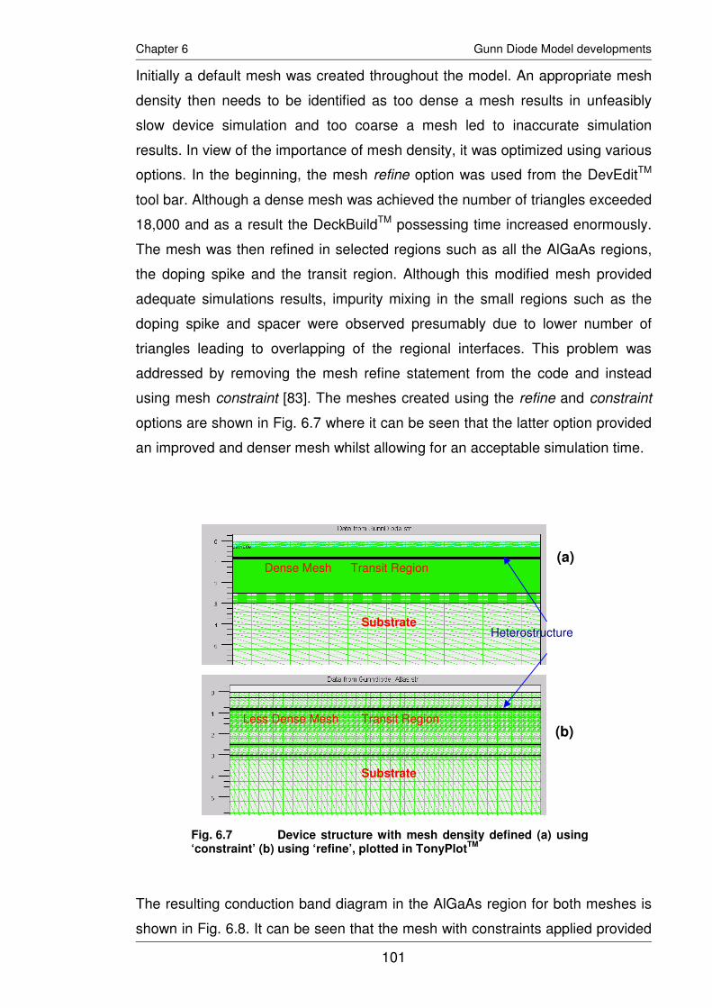
101
Chapter 6 Gunn Diode Model developments
Initially a default mesh was created throughout the model. An appropriate mesh
density then needs to be identified as too dense a mesh results in unfeasibly
slow device simulation and too coarse a mesh led to inaccurate simulation
results. In view of the importance of mesh density, it was optimized using various
options. In the beginning, the mesh refine option was used from the DevEditTM
tool bar. Although a dense mesh was achieved the number of triangles exceeded
18,000 and as a result the DeckBuildTM possessing time increased enormously.
The mesh was then refined in selected regions such as all the AlGaAs regions,
the doping spike and the transit region. Although this modified mesh provided
adequate simulations results, impurity mixing in the small regions such as the
doping spike and spacer were observed presumably due to lower number of
triangles leading to overlapping of the regional interfaces. This problem was
addressed by removing the mesh refine statement from the code and instead
using mesh constraint [83]. The meshes created using the refine and constraint
options are shown in Fig. 6.7 where it can be seen that the latter option provided
an improved and denser mesh whilst allowing for an acceptable simulation time.
The resulting conduction band diagram in the AlGaAs region for both meshes is
shown in Fig. 6.8. It can be seen that the mesh with constraints applied provided
Heterostructure Substrate
Transit Region
Transit Region
Substrate
Dense Mesh
Less Dense Mesh
(a)
(b)
Fig. 6.7 Device structure with mesh density defined (a) using ‘constraint’ (b) using ‘refine’, plotted in TonyPlot
TM

102
Chapter 6 Gunn Diode Model developments
a large number of triangles even in the smallest region, thus yielding a more
realistic conduction band diagram.
The device structure can also be defined in DeckBuildTM through the ATLASTM
command line. The command line codes were written to create 3D rectangular
and cylindrical structures. The structures were created in an order of four distinct
set of commands. The initial mesh was defined with a set of horizontal (x.mesh)
and vertical (y.mesh) meshes with specific spacing between them. The mesh
spacing was defined using parameter spac. After specifying meshes, the regions
and materials were assigned. The electrodes and doping in the regions followed.
Finally the structure was saved and simulated in DeckBuildTM.
During initial model development, convergence issues were experienced which
were attributed to meshes, material parameters and models definition. After
improving models and material parameters, the convergence problem was
narrowed down to number of meshes in regions such as the hot electron injector
(AlGaAs launcher and doping spike regions) and the transit region.
Subsequently, spacing between the meshes was reduced beyond SILVACOTM
recommended maximum number. It was achieved by using spac, which created
Co
nd
uction
Ba
nd
En
erg
y (
eV
)
Less Number of Triangles with ‘Refine Mesh’
Large Number of Triangles with ‘Constraint Mesh’
Fig. 6.8 Conduction band comparative data showing two models with course and dense meshing in the step-graded launcher
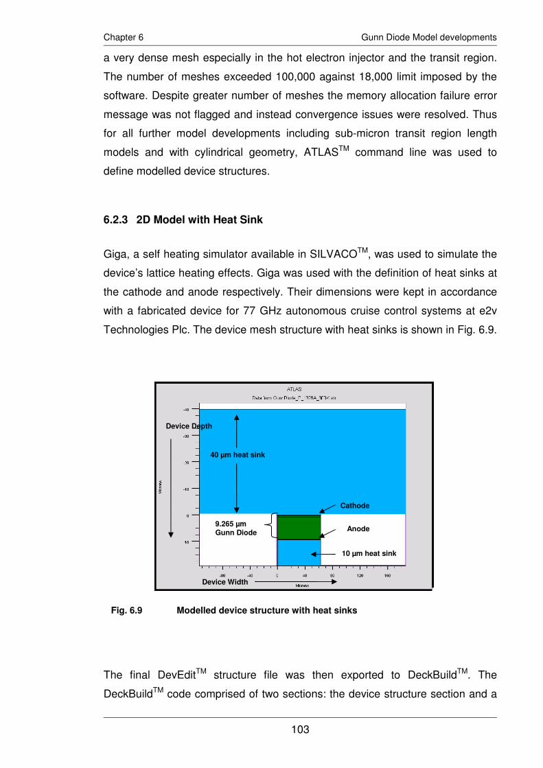
103
Chapter 6 Gunn Diode Model developments
a very dense mesh especially in the hot electron injector and the transit region.
The number of meshes exceeded 100,000 against 18,000 limit imposed by the
software. Despite greater number of meshes the memory allocation failure error
message was not flagged and instead convergence issues were resolved. Thus
for all further model developments including sub-micron transit region length
models and with cylindrical geometry, ATLASTM command line was used to
define modelled device structures.
6.2.3 2D Model with Heat Sink
Giga, a self heating simulator available in SILVACOTM, was used to simulate the
device’s lattice heating effects. Giga was used with the definition of heat sinks at
the cathode and anode respectively. Their dimensions were kept in accordance
with a fabricated device for 77 GHz autonomous cruise control systems at e2v
Technologies Plc. The device mesh structure with heat sinks is shown in Fig. 6.9.
The final DevEditTM structure file was then exported to DeckBuildTM. The
DeckBuildTM code comprised of two sections: the device structure section and a
Device Depth
40 µm heat sink
Cathode
Anode
Device Width
9.265 µm Gunn Diode
10 µm heat sink
Fig. 6.9 Modelled device structure with heat sinks

104
Chapter 6 Gunn Diode Model developments
coding section which defines the material parameters, model definition, methods
and bias conditions. Bias was applied before the start of device simulation, which
was achieved using ATLASTM by initializing the device under zero biased
condition. The zero biased data obtained was then saved for subsequent I-V
simulations. The device DC response was determined to study the device I-V
characteristics. TonyPlotTM was used to display the device simulation results.
The log files and device structure files, created by DeckBuildTM, were saved and
subsequently plotted with TonyPlotTM for analysis [82-84].
6.2.4 3D Rectangular Model Development
The 2D device structure was redefined in DeckBuildTM with a third dimension.
The ‘z’ dimension was defined while keeping the device area similar to the
fabricated device. Fig. 6.10 – 6.11 shows the 3D device structure, where it can
be seen that device layers are in the y-axis and its width in the z-axis. Blaze3D (a
variant of Blaze2D which accounts for third dimension) was used to simulate the
3D device structure.
Fig. 6.10 3D rectangular model epitaxial structure
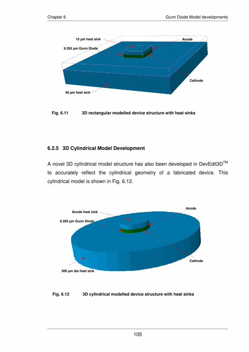
105
Chapter 6 Gunn Diode Model developments
6.2.5 3D Cylindrical Model Development
A novel 3D cylindrical model structure has also been developed in DevEdit3DTM
to accurately reflect the cylindrical geometry of a fabricated device. This
cylindrical model is shown in Fig. 6.12.
300 µm dia heat sink
Cathode
9.265 µm Gunn Diode
Anode heat sink Anode
Fig. 6.12 3D cylindrical modelled device structure with heat sinks
40 µm heat sink
Cathode
9.265 µm Gunn Diode
10 µm heat sink Anode
Fig. 6.11 3D rectangular modelled device structure with heat sinks

106
Chapter 6 Gunn Diode Model developments
6.3 Initial Device Solution
The initial solution for a given model, on which subsequent simulation iterations
are based, is obtained at a bias condition of zero volts. This is because in
ATLASTM the initial values for internal potential and carrier concentration are
based on the device’s doping profile. Through use of the solve init statement the
initial response is calculated and saved as the device structure file shown in Fig.
6.13. This plot shows electron concentration through the device and on the left
side a display bar shows the other options that are available for display in the
device cross section view. By default the display bar only provides the doping
concentration. However, with the addition of the output statement after the
models statement in DeckBuildTM, other options such as electric field, electron
mobility, electron temperature, electron velocity, conduction band and valence
band profile, and charge and current flow lines can also be plotted in the device
cross section view.
After determining initial device solution, DC simulations and device transient
response was obtained as discussed below;
Device length µm
Ele
ctr
on
Co
ncen
trati
on
/c
m3
Tra
nsit
Reg
ion
B
uff
er
Su
bstr
ate
Co
nta
ct
Laye
r
Fig. 6.13 Device model structure cross section view plotted in TonyPlotTM

107
Chapter 6 Gunn Diode Model developments
6.3.1 DC Simulation Results
The DC solution was obtained in DeckBuildTM using the solve statement. The
anode voltage was ramped from 0 to 4 volts with a step size of 0.1V. The file was
then saved and plotted to provide the I-V curve shown in Fig. 6.14, which shows
the start of the negative differential mobility region. The DC solution beyond 4V
could not be achieved due to convergence problems that were later, resolved for
transient simulations. However, it did provide the critical current at the onset of
NDR.
During reverse bias simulations the anode voltage was ramped from 0 to -4V
with a step size of -0.1V. The resulting I-V curve is also shown in Fig. 6.14 and
has been plotted on the positive axis for better visualization.
The modelled device’s asymmetrical I-V response indicates the successful
incorporation of the injector and matches published data and the basic theory
discussed previously.
6.3.2 Transient solutions
Transient solutions are used to obtain a time domain response such as
determining the device oscillating frequency in biased condition. In the Gunn
diode transient solutions for a linear ramp is obtained by specifying parameters
0 1 2 3 40.0
0.2
0.4
0.6
0.8
1.0
1.2
Curr
ent (A
)
Voltage (V)
Model Fwd 300K Model Rev 300K
Fig. 6.14 Model forward-reverse asymmetrical I-V characteristics
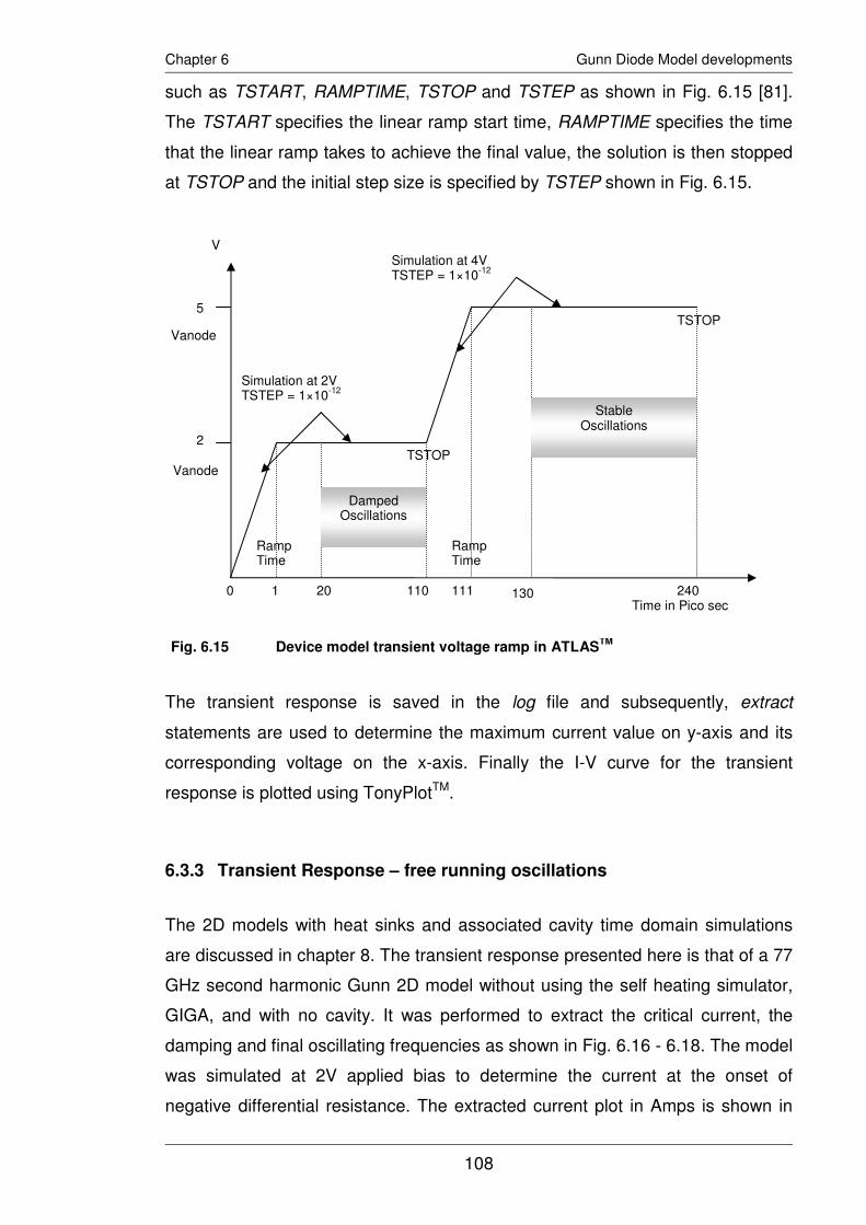
108
Chapter 6 Gunn Diode Model developments
such as TSTART, RAMPTIME, TSTOP and TSTEP as shown in Fig. 6.15 [81].
The TSTART specifies the linear ramp start time, RAMPTIME specifies the time
that the linear ramp takes to achieve the final value, the solution is then stopped
at TSTOP and the initial step size is specified by TSTEP shown in Fig. 6.15.
The transient response is saved in the log file and subsequently, extract
statements are used to determine the maximum current value on y-axis and its
corresponding voltage on the x-axis. Finally the I-V curve for the transient
response is plotted using TonyPlotTM.
6.3.3 Transient Response – free running oscillations
The 2D models with heat sinks and associated cavity time domain simulations
are discussed in chapter 8. The transient response presented here is that of a 77
GHz second harmonic Gunn 2D model without using the self heating simulator,
GIGA, and with no cavity. It was performed to extract the critical current, the
damping and final oscillating frequencies as shown in Fig. 6.16 - 6.18. The model
was simulated at 2V applied bias to determine the current at the onset of
negative differential resistance. The extracted current plot in Amps is shown in
V
Time in Pico sec
5
2
20 0 110 111 240
Simulation at 2V TSTEP = 1×10
-12
Simulation at 4V TSTEP = 1×10
-12
TSTOP
TSTOP
Ramp Time
Vanode
Ramp Time
1 130
Damped Oscillations
Stable Oscillations
Vanode
Fig. 6.15 Device model transient voltage ramp in ATLASTM

109
Chapter 6 Gunn Diode Model developments
Fig. 6.16, which depends on the model width as discussed earlier. The first
damping oscillating transient response is shown in Fig. 6.17 and shows that the
domain is not fully formed resulting in the damping transient response which
eventually died down. The damping transient response although yielding very
high frequency resulting in a power that was very low. Therefore, it was
concluded that at the onset of negative differential resistance the applied
potential and hence the field is not enough to sustain the domain.
Curr
ent
(A)
Transient Oscillations at 2V
Fig. 6.17 Transient response - damping frequency at 2V
Curr
ent
(A)
Transient Simulation at 2V
Fig. 6.16 Transient response - critical current at 2V

110
Chapter 6 Gunn Diode Model developments
The applied bias was increased from 2 to 4 volts (representing a realistic device
operating bias) and the transient response was determined as shown in Fig.
6.18. It can be seen that the domain is quenched during the RF cycle due to a
decrease in terminal voltage below the sustaining voltage. A new domain at the
cathode does not nucleate until the terminal voltage rises above the threshold
value.
6.4 Free-running frequency of oscillation
It has been shown [12] that weak oscillations will occur in a device biased at
voltages below its turn on voltage and that these weak oscillations will be
extremely noisy at low bias voltages due to the excitation of numerous modes
within the transit region (and a reduction in the level of coherence). As the
external bias is increased the level of coherence also increases due to the larger
high-field domains reducing the overall internal electric field in the transit region
and so preventing multiple modes propagating. In addition, as the external bias
voltage increases the oscillation frequency decreases and the RF power
increases. At the threshold (turn on) voltage, the RF power locks onto a single
Curr
ent
(A)
Transient Oscillations at 4V
Fig. 6.18 Transient response - stable oscillations at 4V

111
Chapter 6 Gunn Diode Model developments
frequency defined by the resonant oscillator circuit and a highly coherent output
is observed.
These effects are illustrated in Fig. 6.19 which shows the onset of oscillation,
region of weak oscillation, and turn on voltage of two GaAs Gunn devices. The
plot is taken from [12] and was produced using Monte Carlo simulations of the
free running frequency of GaAs Gunn devices with and without hot-electron
injection (it is noted that the power curve is based on measured values and that
the simulations did not include consideration of an oscillator circuit). This shows
that the free-running frequency of oscillation is reduced as the external field is
increased, meaning that the oscillation frequency of the simulated time-domain
response is typically expected to be higher than that measured from an oscillator
circuit. It also shows that the capability of a device to support sustained
oscillation can be established from simulation of the model at low bias voltages.
The majority of the time-domain simulations were therefore carried out at two
bias voltages: a low voltage (typically about 2 volts) to establish whether the
device was capable of producing sustained oscillations and, where possible, a
higher voltage (about 4 volts) to study the behaviour of the device under realistic
operating conditions.
Fig. 6.19 Monte Carlo simulation results for GaAs Gunn diodes with and without hot electron injection. It is noted that the power curve is taken from measurements of a typical device with hot electron injection, and that an oscillator circuit was not included in the simulation [12].

112
Chapter 6 Gunn Diode Model developments
6.5 Conclusion
A step-by-step process has been discussed to develop a physical model in
SILVACOTM VWFTM environment using ATLASTM as the core tool. It was shown
that in the ATLASTM program flow, the order in which statements are defined is
crucial. The five groups of statements and their order was presented.
Development of the physical model was presented for a state of art GaAs Gunn
diode with a step graded AlGaAs hot electron injector. It includes 2D model, 2D
model with heat sink, 3D rectangular model and a novel 3D cylindrical model
developed for a 77GHz second harmonic graded gap injector Gunn diode.
It was shown that convergence issues were resolved by improving physical
models, selecting correct material parameters and refining meshes in regions
such as hot electron injector and transit region. The spacing between the
meshes was reduced beyond SILVACOTM recommended number by using spac,
which created a very dense mesh. The number of meshes exceeded 100,000
against 18,000 limit imposed by the software. Despite greater number of meshes
the memory allocation failure error message was not flagged. For all further
model developments including sub-micron transit region length models and with
cylindrical geometry, ATLASTM command line was used with spac defined.
The modelled device initial solution, DC simulations and transient responses
were presented that are discussed in chapters 8 and 9. The modelled device’s
asymmetrical I-V response indicated the successful incorporation of the injector.
The transient response presented is that of a 77 GHz second harmonic Gunn 2D
model without using the self heating simulator, GIGA, and with no cavity. It was
performed to extract the critical current, the damping and final oscillating
frequencies. The model was simulated at 2V applied bias to determine the
current at the onset of negative differential resistance. The first damping
oscillating transient response, at 2V applied bias, showed that the domain was
not fully formed resulting in the damping transient response which eventually
died down. It was concluded that at the onset of negative differential resistance
the applied potential and hence the field is not enough to sustain the domain.
The applied bias was increased from 2 to 4 volts (representing a realistic device
operating bias) and the transient response was determined. It was shown that

113
Chapter 6 Gunn Diode Model developments
the domain was quenched during the RF cycle due to a decrease in terminal
voltage below the sustaining voltage.
Finally free running frequency of oscillation was discussed. It was shown that the
free-running frequency of oscillation is reduced as the external field is increased,
meaning that the oscillation frequency of the simulated time-domain response is
typically expected to be higher than that measured from an oscillator circuit. It
was also shown that the capability of a device to support sustained oscillation
could be established from simulation of the model at low bias voltages.

Chapter 7 Physical Models
7.1 Physical Models Used for Device Simulation
The accuracy of the simulated response depends on the choice of material
parameters and the selection of physical models (and their associated
parameters) used. The material and model parameters used were therefore
extensively researched from a variety of sources [3, 29, 65, 85, 86]. Where the
platform did not allow sufficient flexibility to accurately account for the
interdependency of parameters, appropriate C-language functions were written
and incorporated through the in-built C-interpreter [81, 83].
The analytic function based on the work of Caughey and Thomas [87] is used for
modelling field dependant mobility in the contact layers, spacer layers, AlGaAs
launcher and also the transit region for field strengths below the negative
differential mobility (NDM) threshold. For field strengths in the transit region
above the NDM threshold, the Barnes NDM model [88] is used. The Shockley-
Read-Hall (SRH) recombination model [89, 90] is applied in the nominally
undoped AlxGa(1-x)As barrier. The SRH concentration-dependent lifetime model
[89] is used in the rest of the device to account for the varied silicon impurity
concentrations.
For local temperature, self-heating, lattice heat flow and heatsinking effects, Giga
[81], the ATLASTM non-isothermal device modeller module is used. This is based
on the models suggested by Wachutka [91] and accounts for Joule heating along
with heating and cooling due to carrier generation and recombination.
The models used for each material i.e. GaAs and AlGaAs are listed in table 7.1
and are discussed in detail [81]:
114

115
Chapter 7 Physical Models
Table 7.1 Physical models summary
7.2 Mobility Models Used
In the Gunn diode, as in other electron carrier devices, the electrons are
accelerated by the electric field. However, they lose momentum due to numerous
Material Physical Models
GaAs Mobility Conmob – (Concentration Based Mobility)
Analytic – (Caughey Thomas)
Fldmob evsatmod=1 b.elec=2 – (Field Dependent
Mobility with NDR)
Recombination Consrh – (SRH Concentration-Dependent Lifetime
model)
Carrier Statistics
and transport
Boltzmann – (Boltzmann Approximation)
Temperature=300 – (device lattice temperature at 0
bias)
AlGaAs Recombination SRH – (Shockley-Read-Hall)
Mobility Fldmob evsatmod=0 b.elec=2 – (Field Dependent
Mobility without NDR)
GaAs
and
AlGaAs
Carrier Statistics
and transport
Boltzmann – (Boltzmann Approximation)
Temperature=300 – (device lattice temperature at 0
bias)
hcte.el – (Hydrodynamic model for electrons)
GIGA lat.temp - (Lattice Heat Flow Equation)
e.taur.var - (Electron energy relaxation time)
Heat
Sinks
Anode and
Cathode
GIGA - self heating simulator defined to simulate lattice
heating effects as a function of applied voltage.

116
Chapter 7 Physical Models
microscopic scattering processes. These microscopic phenomena are lumped
into macroscopic mobilities, which are included by the mobility and transport
equations during device modelling. The mobility equations used for the Gunn
diode model in the low and high electric field regions will be discussed
individually.
The carriers are almost in equilibrium with the lattice at low field values and so
the electron mobility 0nv has a characteristic low-field value. This low-field value
depends on the phonon and impurity scattering that affects (decreasing its
value). However, the carriers are no longer in equilibrium at high electric fields
and are therefore subjected to a wider range of scattering processes. Therefore,
at high electric fields the drift velocity no longer increases linearly and becomes
saturated or decreases, which is termed as saturation velocity (n
satv ). These
effects must obviously be accounted for using the appropriate models [81].
ATLASTM and its sub-engine Blaze provide various low-field and high-field
models that can be used depending on the device and its operation. The models
used for the simulations will now be discussed.
7.2.1 Low field Mobility Models
Suitable low field models for the simulation were carefully selected. Five
distinctive models and conditions are available in ATLASTM to define the low field
electrical mobility in GaAs and AlGaAs [81]:
• The low-field mobility parameter ‘MUN’(cm2/V.s), can be defined from the
ATLASTM lookup table. The value is defined in the mobility statement for each
region.
• The concentration based mobility model ‘CONMOB’ can be used. The values
for low field mobility at 300K are found from the ATLASTM look-up table for
the doping concentration in each region.
• In order to relate the low field electron mobility with impurity concentration
and temperature, the ‘ANALYTIC’ and ‘ARORA’, may be used.
• A carrier-carrier scattering model (CCSMOB), which relates the low field
mobility to both carrier concentration and temperature can be used.

117
Chapter 7 Physical Models
• Using the unified low field mobility model (KLAASSEN). This model relates
the low field mobility to lattice, carrier-carrier, donor scattering, and
temperature.
7.2.2 AlGaAs Default Low field Mobility Model
For the un-doped AlxGa1-xAs regions the Constant Low Field Mobility model was
used which is independent of the doping concentration, carrier densities and
electric field. The electron mobility values in this model are determined using the
following formula:
MUNT
LUNn
TMv
−
=
3000 ……………………………...…………………(7.1)
where LT is the lattice temperature in degrees Kelvin, MUN is the undoped
mobility value in cm2/Vsec and TMUN is the temperature dependent coefficient
whose value is taken from the SILVACOTM lookup table (TMUN=1.5) [81]. These
parameters are specified in the material statement as shown in table 7.2. The
simulations were performed at KTL 300= which resulted in an electron mobility
equal to the undoped mobility value (MUN) defined for each Al concentration. The
temperature dependent co-efficient TMUN was ignored. The AlGaAs mobility
values (MUN), which were defined separately for each AlGaAs region due to
dependability on the Al concentration, are shown in table 7.2 [81].
AlxGa1-xAs Region Statement Code
x=0.017 mobility region=11 mun=4700
x=0.08 mobility region=10 mun=4300
x=0.16 mobility region=9 mun=3400
x=0.24 mobility region=8 mun=2400
x=0.32 mobility region=7 mun=800
Table 7.2 Mobility values for AlxGa1-xAs regions [52]

118
Chapter 7 Physical Models
7.2.3 GaAs Concentration Dependent Low Field Mobility Model
For a doped GaAs region the electron mobility depends on the impurity levels in
each region alongwith the operating temperature. The Concentration Based
Mobility conmob was therefore defined for all GaAs regions. The SILVACOTM
default library has built in values for all GaAs concentration values at 300K. And
this default data was used during the simulations. To take into account
temperature effects on the electron mobility the analytic model was used which
allowed the temperature to be varied from 77 to 450K.
7.2.4 GaAs Analytic Low Field Mobility Model
The Caughey Thomas Analytic Low Field Mobility model [87] was used for the
GaAs regions. The model was used to specify doping and temperature
dependent low field mobilities using the following equation:
CAUGCAUG
CAUGCAUG
CAUG
CRITN
CAUG
L
LNU
CAUGLNU
CAUG
LNU
CAUGn
N
NT
TM
TM
TMv
∆Γ
+
−
+
=
.300
1
300300
300
12
1
0
αβ
α
cm2/V.sec…(7.2)
A description of the parameters used in equation 7.2 along with their values is
shown in table 7.3. The model is activated by defining both conmob and analytic
in the models statement.
The default mobility values for NU
CAUGM1
and NU
CAUGM2
were used for all GaAs regions
except the transit region, where the parameters were defined to achieve the
6300 cm2/V.sec [88], which was achieved through iterative simulations.
Optimised values for the mobilities at highest and lowest Al concentrations were
found as 9401 =NU
CAUGM and 86851 =NU
CAUGM respectively, which were used for
subsequent simulations. The temperature dependent fitting parameters CAUGα ,
CAUGβ and CAUGΓ were defined using the C-interpreter function. The default value
for CAUG∆ was kept as 1 to account for the increasing concentration effect on the
electron mobility [81].

119
Chapter 7 Physical Models
Parameter Description Value Units
NU
CAUGM1
Mobility at highest concentration value,
depends on impurity doping
- cm2/Vsec
NU
CAUGM2
Mobility at lowest concentration. Depends on
impurity doping
- cm2/Vsec
CAUGα Temperature dependent fitting parameters 0 Arbitrary
CAUGβ Temperature dependent fitting parameters 0 Arbitrary
CAUGΓ Temperature dependent fitting parameters 0 Arbitrary
CAUG∆ Temperature dependent fitting parameters 1 Arbitrary
CRITN
CAUGN Caughey Thomas critical concentration level 16108.2 × cm-3
N Impurity concentration defined for individual
region
- cm-3
LT Temperature 300 K
Table 7.3 Caughey Thomas Analytic Low Field mobility model parameters (300K) [87]
7.2.5 Parallel Electric Field Dependent Mobility Model
Two types of electric field dependent mobility (fldmob) models are available in
ATLASTM. The models are named as the Standard Mobility model and Negative
Differential Mobility model, both of which contain appropriate default parameter
values for different materials. The models are defined by specifying evsatmod
along with the fldmob in the models statement. The evsatmod specifies which
parallel field dependent mobility model should be used for electrons, which are
defined as [81]:
• evsatmod=0 allows the application of standard Mobility model
• evsatmod=1 implements the GaAs negative differential mobility saturation
model.

120
Chapter 7 Physical Models
• evsatmod=2 implements the simplified field dependent velocity model.
The standard electric field based mobility model is applied and the
temperature dependent mobility is not used.
The standard mobility model was used for AlGaAs step graded heterostructure
region. The standard mobility model is defined in terms of electron saturation
velocity, which is a function of applied electric field. The model is implemented in
ATLASTM using the following Caughey Thomas expression, which provides a
smooth transition between low-field and high field behaviour [87]:
n
n
satn
n
nn
v
EvvEv
β
β
1
0
1
1)(
+
= ………………………………………..(7.3)
where, satnv is the electron saturation velocity, nβ is a constant whose value for
both AlGaAs / GaAs and was taken as 1 from the SILVACOTM reference tables.
The low field electron mobility, 0nv , is determined from equations 7.1 and 7.2 for
AlGaAs and GaAs respectively. A similar equation for holes is also available but
has not been used, since holes do not play any role in the simulations due to +n
dopant use.
The Barnes Negative Differential Mobility model [88] was used in the transit
region at high electric filed. The electron saturation velocity, as a function of
electric field, is given by:
N
N
N
CRIT
N
CRIT
satnn
n
E
E
E
E
E
vv
EvΓ
Γ
+
+
=
1
)(
0
……………………..………………..(7.4)
where satnv is the electron saturation velocity, 0nv is the low field electron
mobility, N
CRITE is the critical electric field in cmV / , NΓ is a constant equal to 2 for
GaAs and E is the electric field. The critical electric field for GaAs was defined as
33.4 10N
CRITE = × .

121
Chapter 7 Physical Models
It should be noted here that for both standard and negative differential mobility
models, an empirical temperature dependent saturation velocity for GaAs is
implemented as:
Lsatn Tv46 102.1103.11 ×−×= scm / …………………..………….(7.5)
where, LT is the temperature in degree Kelvin. For the device model simulated at
300K, a GaAs saturation velocity value of scm /107.7 6× was used during device
simulations.
7.3 Carrier Generation – Recombination Models
The processes responsible for carrier generation and recombination fall under
following six main categories:
• Phonon transitions
• Photon transitions
• Auger transitions
• Surface recombination
• Impact ionization
• Tunnelling
In ATLASTM this six generation-recombination mechanisms are represented
using different models. For Gunn diode modelling, the Shockley-Read-Hall
(SRH) recombination (phonon Transition) and SRH Concentration-Dependent
Lifetime (Photon Transition) models have been used for AlGaAs and GaAs
regions respectively as listed in table 7.1.
7.3.1 Shockley-Read-Hall (SRH) Recombination
Phonon transition within a semiconductor is due to a trap or defect within its
forbidden gap. The theory of phonon transition was discovered first by Shockley

122
Chapter 7 Physical Models
and Read [89], and then later by Hall [90]. The Shockley-Read-Hall (SRH)
recombination model was used for the AlGaAs regions and implemented as:
Ε−++
Ε+
−=
L
TRAPieN
L
TRAPieP
ieSRH
kTnp
kTnn
npnR
expexp 00
2
ττ
……..(7.6)
where 0Nτ and 0Pτ are the electron and hole life times, which were defined for
each individual AlxGa1-xAs region. The values were calculated using the virtual
crystal approximation formula for both GaAs and AlAs. The values for these
materials were taken from the SILVACOTM reference tables. TRAPΕ indicates the
trap energy and intrinsic Fermi level difference in electron volts. Its default value
)0( =ETRAP was used to correspond to efficient recombination of one trap layer
present in the material. LT is the lattice temperature in degrees Kelvin. The
model was activated by defining srh in the model statement for the AlGaAs
region.
7.3.2 SRH Concentration-Dependent Lifetime model
The concentration based SRH model was used for the GaAs regions due to the
different impurity concentration level in each. The modified SRH model with
carrier life time as a function of doping concentration is implemented in ATLASTM
[81, 92] as follows:
Ε−++
Ε+
−=
L
TRAPien
L
TRAPieP
ieSRH
kTnp
kTnn
npnR
expexp
2
ττ
…….… (7.7)
where
EP
P
SRH
total
P
SRH
total
PP
N
NCN
N
NBPAP
+
+
= 0ττ ………………….………………………(7.8)
EN
N
SRH
total
N
SRH
total
Nn
N
NCN
N
NBNAN
+
+
= 0ττ …………………..…………………….(7.9)

123
Chapter 7 Physical Models
Here, N is the carrier concentration level and the constant values AN, BN were
taken from the SILVACOTM reference tables. N
SRHN and P
SRHN are the SRH
concentration levels for electrons and holes respectively. totalN is the total carrier
concentration level. 0Nτ and 0Pτ are the electron and hole life times as discussed
earlier. Most of these parameters are well defined for GaAs in the SILVACOTM
default library at 300K. And so the default values were used in the model [81].
7.4 Carrier Statistics and Transport
Within a semiconductor the thermal equilibrium of electrons at temperature LT
obeys Fermi-Dirac statistics. The electron occupation probability for a given
energy, )(Εf , is given as [81]:
Ε−Ε+
=Ε
L
F
KT
f
exp1
1)( …………………………….…………….(7.10)
If LF KT>>Ε−Ε (non-degeneracy) then the equation can be approximated as:
Ε−Ε=Ε
L
F
KTf exp)( …….……………………………………….(7.11)
The above approximation is known as the Boltzmann statistic. The Boltzmann
approximation simplifies the calculations whilst yielding satisfactory results. It
was used in the model that minimized convergence issues as compared to the
Fermi-Dirac statistics. In ATLASTM the use of the Boltzmann statistic has been
set at its default implementation [81].
The transport models, Drift Diffusion, energy balance and hydrodynamic models
available in ATLASTM are discussed. In the Gunn diode model the carriers were
selected as electrons. The electrons equations are presented only.

124
Chapter 7 Physical Models
7.4.1 Drift Diffusion Model
The Drift Diffusion model is used as default in ATLASTM to model carrier
transport or current density. It applies approximations and simplifications to the
Boltzmann Transport Equation. It does not introduce any independent variable in
addition to electrostatic potential and the electron concentration. This model
although simple, ignores non-local transport effects such as velocity overshoot
and diffusion due to carrier temperature. Resultantly, its accuracy decreases for
sub micron devices. The current density J
for electrons (n ) is given as;
n n nJ q nE qD nµ= + ∇
………..…………………………………….(7.12)
where nµ is the electron mobility, E
is the local electric field in cmV / , D is the
diffusion coefficient, which is calculated using Einstein’s relationship as;
n n
kTD
qµ= ……..………………………………………………….(7.13)
7.4.2 The Energy Balance and Hydrodynamic Transport Models
In ATLASTM, the energy balance and hydrodynamic transport models are
available as current density non-local models. These models uses additional
coupling of the current density to the carrier temperature. The Energy Balance
Transport Model is derived from the Boltzmann Transport Equation using
Stratton derivation [93, 94]. It is simplified by applying some assumptions into the
hydrodynamic model [95-97].
Three energy balance transport equations for electrons comprising of energy
balance equation, current density and energy flux are as follows;
( )1 3. .
2n n n n n
kS J E W nT
q t
δλ
δ∗∇ = − −
……...……………………….(7.14)
.T
n n n n nJ qD n q n qnD Tµ ψ= ∇ − ∇ + ∇
……………………………….(7.15)
nnn Bn n
kS K Tn J T
q
δ = − ∇ −
…………………………….……….(7.16)

125
Chapter 7 Physical Models
The energy balance transport equations simplify into the hydrodynamic transport
equations by substituting 1nλ∗ =
and 5
2n
δ = . The hydrodynamic transport
equations are given as;
( )1 3
. .2
n n n n
kS J E W nT
q t
δ
δ∇ = − −
………………...……………….(7.17)
T
n n n n nJ qD n q n qnD Tµ ψ= ∇ − ∇ + ∇
………………….…………….(7.18)
5.2
nn Bn n n
kS K T J T
q
= − ∇ −
……………………….…….……….(7.19)
where,
nS
is the electron energy flux density
nD is the thermal diffusion coefficient (equation 7.13)
nW is the energy density loss rates for electrons (equation 7.29)
BnK is the thermal conductivity of electrons given as;
2
Bn n n
kK qn T
qµ
= …………………………..………………….(7.20)
The hydrodynamic model provides realistic results and better convergence. It
was implemented in the Gunn diode model using parameter hcte.el on the
models statement.
7.5 GIGATM – Self Heating Simulator
Lattice heat flow and general thermal environment simulation in the model has
been implemented using GIGATM, a self heating simulator, which extends
ATLASTM capabilities in the DeckBuildTM environment. GIGATM is based on the
models suggested by Wachutka [91], which precisely accounts for the Joule
heating and heating and cooling due to carrier generation and recombination.
Ambient temperature conditions, realistic heat-sinks and thermal impedances are
also accounted for. Additionally, all the material and transport parameters

126
Chapter 7 Physical Models
defined for each region are made lattice temperature dependent throughout the
model.
Statement Parameter Details
material hc.comp Heat Capacity model
tcon.power Thermal conductivity model
models lat.temp Lattice Heat Flow Equation
e.taur.var Electron energy relaxation time
thermcontact ext.temper Heat sink temperature
Heat sink electrodes are defined
with dimensions
Table 7.4 GIGATM
– self heating simulator parameters
7.5.1 The Lattice Heat Flow Equation
GIGATM adds the following lattice heat flow equation to the primary equations
that are solved by ATLASTM:
( )L
TC T H
tκ
∂= ∇ ∇ +
∂ ………………….………………………….(7.21)
where,
C is the heat capacitance per volume
κ is the thermal conductivity
H is the heat generation
LT is the local lattice temperature
The heat capacitance can also be defined as pC Cρ= , where ρ is the density of
material and pC is the specific heat. The lattice heat flow equation is included
during simulation by defining lat.temp parameter on the models statement.

127
Chapter 7 Physical Models
7.5.2 Heat Capacity
The temperature dependent heat capacity for defined regions in a structure is
modelled as [98];
( ) 300 1
1
300
1300
300
L
L
L
T
C T C CT C
C
β
βρ
−
= +
+
(J/cm3/K) …………………(7.22)
where,
( )LC T is the temperature dependent heat capacity (J/cm3/K)
ρ is the mass density (g/cm3)
300C is the specific value for heat at 300K (J/K Kg)
1C is the material dependent specific value for heat (J/K Kg)
β is the material dependent fitting parameter
The values of ρ , 300C , 1C , and β for both GaAs and AlAs are listed in table 7.5
[86]. They were defined using the C-interpreter functions. The temperature
dependent heat capacity for each region was modelled by specifying the
parameter hc.comp on the material statement.
Parameter Material Units
GaAs AlAs
ρ 5.32 3.76 g/cm3
300C 322 441 J/K Kg
1C
50 50 J/K Kg
β 1.6 1.2 -
Table 7.5 Heat Capacity parameters

128
Chapter 7 Physical Models
In case of ternary compound (AlxGa1-xAs), ( )LC T is calculated by linear
interpolation.
7.5.3 Thermal Conductivity
The value of thermal conductivity, κ , for each region is defined by specifying the
parameter tcon.power on the material statement. It uses the following equation;
.
( . )( )
300
C
C
T NPOW
T CONSTT
Tκ =
(W/cm.K) ………………………………….. (7.23)
where,
κ is the thermal conductivity
T is the lattice temperature
.C
T CONST is the thermal conductivity at 300K
.C
T NPOW is the fitting parameter
The value of thermal conductivity at 300K ( .C
T CONST ) and fitting parameter (
.C
T NPOW ) are defined using the C-interpreter functions as listed in table 7.6 [34,
85, 86].
Parameter Material Units
GaAs AlAs
.C
T CONST 0.46 0.8 W/cm.K
.C
T NPOW 1.25 1.37 -
Table 7.6 Thermal Conductivity parameters
129
Chapter 7 Physical Models
In case of ternary compound (AlxGa1-xAs), .C
T CONST and .C
T NPOW are
calculated as;
( )1
.11 . .
. .
AlGaAs
C
AlAs GaAs bowing
C C
T CONSTx xx com x com
T CONST T CONST C
=− × −
+ +
(W/cm) …... (7.24)
( )1 . .AlGaAs GaAs AlAs
C C CT NPOW x com T NPOW x com T NPOW= − × + × (.K) ……... (7.25)
where,
.x com is the composition fraction
bowingC is the bowing factor (W/cm.K)
The bowing factor ( bowingC ) compensates sudden change of thermal conductivity
due to changing composition fraction ( .x com ). The .C
T NPOW parameter is
calculated by linear interpolation using Vegards law since experimental data
other than 300K is currently not available [86].
7.5.4 Heat Generation
In GIGATM, the heat generation term H from equation 7.21 is set to zero for
insulators. For conductors it is given as;
( )2
divVH
ρ= (J/cm3/K) ………………………………………….. (7.26)
where,
V is the voltage in mV/K
ρ is the mass density in g/cm3
In Gunn diode model hcte.el is specified on the models statement. It uses
hydrodynamic model for electrons only since holes do not play any role in the
carrier transport effects. The heat generation ‘H’ is given as;
.pn gH W E U J E= + +
(J/cm3/K) …………………………………. (7.27)
where,

130
Chapter 7 Physical Models
gE U is the recombination heat power
nW is the Joule heating term
.pJ E
is the Peltier Thomson Heat power
The recombination heat power (gE U ) is the product of band gap energy and the
net generation-recombination rate U . The net generation-recombination rate is
defined as;
A A
SRH n p n pU R R R G G= + + − − (/cm3.s) ………………….……….. (7.28)
where,
SRHR is the SRH recombination rate (equation 7.6 and 7.7)
,A A
n pR R are the Auger recombination rates
,n pG G are the impact ionization rates
The carriers are heated due to lattice temperature increase and they exchange
energy with the lattice using recombination and regeneration processes
(equation 7.28). Both these effects are taken into account by the Joule heating
term n
W which is defined as the energy density loss rate.
The energy density loss rate for electrons is given as;
( )( )3 3
2 . 2
n L A
n n SRH g n n
k T TW n kT R E G R
taurn el
−= + + − (/cm3.s) ……….. (7.29)
where,
.taurn el is the electron energy relaxation time.
7.5.5 Electron Energy Relaxation Time
In ATLASTM no temperature dependent electron energy relaxation model is
available. The electron energy dependent model was used instead. It is activated
by using e.taur.var on the models statement. The model parameters listed in

131
Chapter 7 Physical Models
table 7.7 [85] are defined on the material statement. The electron energy energy
nW
is given as;
3
2
energy
n nW kT= (eV) …………………………………………..….. (7.30)
The electron energy relaxation time is determined by quadratically varying values
with respect to electron energy energy
nW , by using following relations;
. 1, . 1
. . 2, . 2
. 3, . 3
energy
n
energy
e n
energy
n
TRE T W TRE W
taurn el TRE T W TRE W
TRE T W TRE W
τ
<
= = =
>
(eV) ……………….. (7.31)
Parameter Value Units
. 1TRE T 0.5 ps
. 2TRE T 1.24 ps
. 3TRE T
1.74 ps
. 1TRE W
0.06 eV
. 2TRE W
0.3 eV
. 3TRE W 4.5 eV
Table 7.7 Electron energy relaxation time parameters
7.5.6 Thermal Boundary Conditions
In ATLASTM, the thermal boundary condition provides total energy flux after the
lattice heat flow equation is solved. It is given by;
1( )
boundary
thermal
L
thermal
J T TempR
= − ………..…………………….……... (7.31)

132
Chapter 7 Physical Models
where,
LT is the lattice temperature
Temp is the temperature defined on the thermcontact statement
thermalR is the thermal resistance given as;
1thermalR
Alpha= ………..………………………………….……. (7.31)
The parameter Alpha is defined on the thermcontact statement. The
thermcontact statement also defines the position of the thermal contact (heat
sink) and temperature Temp . In the Gunn diode model two thermal boundary
conditions were defined for Cathode and anode heat sinks respectively. The
parameter 2.5Alpha = was defined.
7.6 C-Interpreter Functions
Some of the physical models used in ATLASTM can be modified using the built-in
C-language interpreter. C-interpreter functions are particularly useful to precisely
define material parameters not available in ATLASTM reference tables. The C-
interpreter functions containing analytic model descriptions which were written
are listed in table 7.8.
Function Model Description
f.bandcomp Band Gap Composition based band gap.
f.bandcomp parameter is defined in the material statement.
f.vsatn Saturation
Velocity
Composition and temperature dependent saturation
velocity.
f.vsatn parameter is defined in the material statement.
f.munsat Mobility Determines the temp dependent mobility. Set by fldmob
evsatmod=0.
f.enmun parameter is defined in the material statement.
f.enmun Mobility Determines temperature dependent low field mobility.
f.enmun parameter is defined in the mobility statement.
f.tcap GIGA Thermal capacity in Giga.
f.tcap parameter is defined in the material statement.
f.tcond GIGA Thermal conductivity in Giga.
f.tcond parameter is defined in the material statement.
Table 7.8 C-Interpreter Functions used in model development

133
Chapter 7 Physical Models
7.7 Conclusion
The accuracy of the simulated response depends on the choice of material
parameters and the selection of physical models (and their associated
parameters) used. The material and model parameters used were therefore
extensively researched from a variety of sources. They have been presented and
discussed, which were carefully selected for each layer depending on the
material and carrier concentration in the region. It included Mobility models,
Carrier Generation-recombination models, Carrier Statistics and Transport
models and GIGATM Self Heating Simulator. It was shown that the analytic
function based on the work of Caughey and Thomas is used for modelling field
dependant mobility in the contact layers, spacer layers, AlGaAs launcher and
also the transit region for field strengths below the negative differential mobility
(NDM) threshold. For field strengths in the transit region above the NDM
threshold, the Barnes NDM model is used. The Shockley-Read-Hall (SRH)
recombination model is applied in the nominally undoped AlxGa(1-x)As barrier.
The SRH concentration-dependent lifetime model is used in the rest of the
device to account for the varied silicon impurity concentrations.
The ATLASTM non-isothermal device modeller module, Giga, used for local
temperature, self-heating, lattice heat flow and heatsinking effects have been
discussed. It is based on the models suggested by Wachutka and accounts for
Joule heating along with heating and cooling due to carrier generation and
recombination. Finally, it was shown that where the platform did not allow
sufficient flexibility to accurately account for the interdependency of parameters,
appropriate C-language functions were written and incorporated through the in-
built C-interpreter.
Chapter 8 Gunn diode Results: DC Analysis
8.1 Introduction
The simulated DC characteristics of the model are presented in this chapter.
They were used to study hot electron injection doping spike. The doping spike
carrier concentration optimum value was determined using a modelled-measured
approach.
In order to examine the accuracy of the developed model a comparison to
measured data needs to be made. A large amount of data from production and
engineering testing carried out at e2v Technologies Plc was made available for
this purpose. The available data included the characteristics of 77 GHz (1.65 µm
transit region device) devices with a range of epitaxial structures which were
measured over a range of temperatures. Also available was data from a new 125
GHz second harmonic device and 94 GHz fundamental device. A relatively
constant I-V current is
The Gunn diodes epitaxially grown at The University of Manchester were
processed / packaged at e2v technologies Plc. They were die-packaged and
etched to current (nominally 750-1200mA) to reduce heat generation and get
better heat sinking. Resultantly, relatively constant current levels were achieved
in the I-V relationships despite reducing device transit region length and
increasing its doping.
8.2 Advanced Step Graded Gunn Diode Modelled–Measured Results
The advanced 77 GHz second harmonic GaAs Gunn diodes discussed here
incorporate a step-graded AlGaAs hot-electron launcher, and are commercially
manufactured in volume by e2v Technologies (UK) Plc. for use in 77GHz
automotive Autonomous Cruise Control (ACC) systems. Tight specifications are
placed on parameters such as RF output power, applied voltage controlled
frequency tuning range and the oscillation frequency’s temperature dependence.
134

135
Chapter 8 Gunn diode Results: DC Analysis
These parameters are all highly dependant on hot-electron injector composition,
especially carrier concentration in the injector’s doping spike [2, 3].
The hot electron injector effectiveness was evaluated using the 77 GHz model.
The doping spike carrier concentration, DC I-V characteristics and doping spike
effects on I-V curves are discussed below.
8.2.1 Doping Spike Carrier Concentration
The hot electron injector, situated between the n+ cathode contact layer and the
n- transit region, consists of two main components: a graded AlGaAs launcher
and a doping spike which is required to modify the forward-bias downstream
electric field in the transit region. As shown in fig. 8.1, in its absence a depletion
region is formed behind the launcher which prevents the nucleation of high-field
domains. With the increase of applied potential, the negative-field gradient rises
and as a result the depletion region grows forming a dead zone. The dead zone
at the start of transit region reduces the performance of the launcher. The dead
zone eventually diminishes as the applied voltage is increased.
The device model with +
n doping spike (cc 318101 −× cm ) resulted in the positive
electric field gradient, which keeps the electron concentration throughout the
1.5 2.0 2.5 3.0 3.51e13
1e14
1e15
1e16
1e17
1e18
1e19
ContactLayer
Transit Region
AlGaAs Launcher
Ele
ctr
on
Co
ncen
tra
tion
(cm
-3)
Device Distance (µm)
ContactLayer
Fig. 8.1 The effects of the doping spike (cc 1×10¹⁸
cm-3
) on electron concentration in the transit region (——; spike present, -----; spike absent)

136
Chapter 8 Gunn diode Results: DC Analysis
transit region as shown in Fig. 8.1. Concomitantly it eliminated the depletion
region, thereby ensuring the elimination of the dead zone and leading to high
efficiency of the hot electron injector. This compares well to previous simulations
results obtained and published by another group using SILVACOTM [10]. This
greatly increased confidence in the developed model.
8.2.2 DC I-V Characteristics of 77 GHz second Harmonic GaAs Gunn
A comparison of the simulated I-V characteristics and measured data at
temperature 300K is shown in Fig. 8.2. The measured results are from a
manufactured device, and supplied by ‘e2v Technologies Plc’. It can clearly be
seen that the simulated I-V characteristics in both forward and reverse bias
match well to those of an actual device thus validating the use of physical
models selected for the simulations. It is noted that in forward bias the simulated
response beyond three volts shows greater negative differential resistance than
the measured data. The higher negative differential is probably due to the ideal
heat sinks higher efficiency and lower resistance values used in the simulation.
8.3 Doping Spike Effects
To compliment experimental data and investigate the relationship between
doping spike carrier concentration and Iasym, the model was simulated with
0.0 0.5 1.0 1.5 2.0 2.5 3.0 3.5 4.00.0
0.2
0.4
0.6
0.8
1.0
1.2Reverse IV Curves
Cu
rren
t (A
)
Voltage (V)
Measured 1928A 300K Model 1928A 300K
Forward
IV Curves
Fig. 8.2 Modelled and measured forward - reverse I-V curves.

137
Chapter 8 Gunn diode Results: DC Analysis
varying carrier concentration ( 18 32 10 cm−× , 318101 −× cm , 17 37.5 10 cm
−× , and
317105 −× cm ) shown in Fig. 8.3. It can be seen that as the doping spike carrier
concentration decreases the injector performance degrades and as a result the
asymmetry increases. Since the injector does not play any role being at the end
of the transit region during reverse bias condition, similar reverse I-V curve could
be seen in the Fig. 8.4.
0.0 0.5 1.0 1.5 2.0 2.5 3.0 3.5 4.00.0
0.2
0.4
0.6
0.8
1.0
1.2
Forward
bias
1.28
1.48
1.17
1.16
Curr
ent (A
)
Voltage (V)
Spike cc = 2x10¹⁸
cm-3
Spike cc =1x10¹⁸
cm-3
Spike cc = 5x10¹⁷
cm-3
Spike cc =2.5x10¹⁷
cm-3
Reverse bias
Fig. 8.4 Effects of variation in doping spike carrier concentration on simulated I-V characteristics (numbers next to forward bias curves represent calculated asymmetry values)
Electron Concentration with Increasing Spike at 0.3 volts
Device Distance along the length in microns
Ele
ctro
n C
oncentr
ation (
cm
3)
Transit Region
Fig. 8.3 Electron concentration with changing doping spike carrier concentration (cc)

138
Chapter 8 Gunn diode Results: DC Analysis
Fig. 8.5 shows the Iasym plotted verses doping spike carrier concentration. It can
be seen that although Iasym decreases as the carrier concentration increases,
which agrees with the trend noted for the experimental data, there is a small
discrepancy between the absolute measured and simulated values. However
qualitatively, it shows the same trend and is remarkably reproduced. This
discrepancy was the result of inaccurate representation of the electric field and
current flow through the device inherent to the method used for scaling the 2D
model to obtain the correct device area. This has a much greater effect when
modelling the Gunn diode which is a ‘field driven’ device, than with voltage or
current driven devices for which SILVACOTM was originally intended. These
results were published [99]. Cylindrical device geometry was defined to take into
account cylindrical geometry of the manufactured device.
A full 3D cylindrical model was developed and results compared to that of a 2D
model. This computationally expensive (tens times than a 2D model) full 3D
cylindrical model [100] was developed using SILVACOTM ATLASTM version
5.12.1 in order to ensure that the modelled electric field across the device
realistically represented that in an actual device [100]. However, due to the
improved meshing capabilities of the since released version 5.12.32 of
SILVACOTM ATLASTM, a cylindrical device geometry can now be defined and
0.0 0.5 1.0 1.5 2.01.1
1.2
1.3
1.4
1.5
1.6
1.7 Simulated Measured
Curr
ent asym
metr
y
Doping spike carrier concentration (1018
cm−3
)
Curve fit to measured data
(3rd order exponential decay)
Fig. 8.5 Simulated and measured asymmetry values versus doping spike carrier concentration

139
Chapter 8 Gunn diode Results: DC Analysis
applied to a 2D model. After verification that a 2D model using the new meshing
technique produced similar results to the full 3D model, the method was adopted
and a large reduction in computational time obtained for subsequent simulations.
8.4 Measured 77 GHz Devices Data Comparison with Modelled Devices
In order to further investigate the accuracy of the model, its simulated response
was compared to the measured results from devices with slightly different
epitaxial structures (the main differences are the doping spike carrier
concentrations) shown in table 8.1. Ambient temperature variation is also
included in both simulated and measured data.
Wafer Name Doping Spike Carrier
Concentration (cm-3
)
Transit Region
Length (µm)
Transit Region Carrier
Concentration (cm-3
)
VMBE 1928A 1×10¹⁸
1.65 1.1×10¹⁶
VMBE 1900 5×10¹⁷
1.65 1.1×10¹⁶
VMBE 1909 7.5×10¹⁷
1.65 1.1×10¹⁶
Table 8.1 Measured devices with slightly different epitaxial structures – doping spike carrier concentration variation
The results for each epitaxial structure will now be discussed.
8.4.1 Doping Spike Carrier Concentration 1××××1016 cm-3 Modelled Device Results (VMBE 1928A)
The forward and reverse I-V curves of a measured device (VMBE 1928A) and
modelled device 1928A are shown in Fig. 8.6. Doping spike with carrier
concentration 1×1018 cm-3 was used in both the modelled and measured devices.
Both modelled and measured data compared very well. The difference in
modelled forward I-V curve, showing higher negative differential resistivity, at
around 3V and onwards is thought due to the heat sinks higher efficiency.

140
Chapter 8 Gunn diode Results: DC Analysis
Modelled and measured temperature curves for VMBE 1928A devices are shown
in Fig. 8.7. The I-V curves were plotted for an ambient temperature of 300K and
323K respectively. Upon increasing the temperature to 323K the injector
effectiveness is reduced and as a result the modelled device’s current saturated
at a lower value which is in agreement with published theoretical data. The
effects of ambient temperature variation on the simulated and measured results
resulted in a close match. This further validates the developed model and use of
the GIGA simulator.
0.0 0.5 1.0 1.5 2.0 2.5 3.0 3.5 4.00.0
0.2
0.4
0.6
0.8
1.0
1.2
Curr
ent
(A)
Voltage (V)
Measured VMBE 1928A 300K
Measured VMBE 1928A 323K
Modelled VMBE 1928A 300K
Modelled VMBE 1928A 323K
Forward IV Curve
Reverse IV Curve
Fig. 8.7 VMBE 1928A Temperature forward - reverse I-V curves
0.0 0.5 1.0 1.5 2.0 2.5 3.0 3.5 4.00.0
0.2
0.4
0.6
0.8
1.0
1.2
Curr
ent (A
)
Voltage (V)
Measured VMBE 1928A 300K
Modelled VMBE 1928A 300K
Forward IV Curve
Reverse IV Curve
Fig. 8.6 VMBE 1928A Modelled and measured forward - reverse I-V curves

141
Chapter 8 Gunn diode Results: DC Analysis
8.4.2 Doping Spike Carrier Concentration 5××××1017 cm-3 Modelled Device Results (VMBE 1900)
The spike doping carrier concentration was reduced from 1×1018 cm-3 to 5×10¹⁷
cm-3. Both simulated and measured devices yielded the asymmetrical response
shown in Fig. 8.8. A good match can be seen between the modelled and
measured data especially in reverse bias conditions. Again the forward I-V curve
showing more negative differential resistance is attributed to the higher efficiency
of the ideal heat sinks used in the modelled device.
Fig. 8.9 shows the temperature simulation for VMBE 1900 with reduced spike
carrier concentration. Again the modelled reverse I-V curve matched closely to
the measured data.
0.0 0.5 1.0 1.5 2.0 2.5 3.0 3.5 4.00.0
0.2
0.4
0.6
0.8
1.0
1.2
1.4
1.6
1.8
Curr
ent
(A)
Voltage (V)
Measured VMBE 1900 300K
Measured VMBE 1900 323K
Modelled VMBE 1900 300K
Modelled VMBE 1900 323K
Forward IV Curve
Reverse IV Curve
Fig. 8.9 VMBE 1900 Temperature forward - reverse I-V curves
0.0 0.5 1.0 1.5 2.0 2.5 3.0 3.5 4.00.0
0.2
0.4
0.6
0.8
1.0
1.2
1.4
1.6
1.8
Curr
ent
(A)
Voltage (V)
Measured VMBE 1900 300K
Modelled VMBE 1900 300K
Forward IV Curve
Reverse IV Curve
Fig. 8.8 VMBE 1900 Modelled and measured forward - reverse I-V curves

142
Chapter 8 Gunn diode Results: DC Analysis
8.4.3 Doping Spike Carrier Concentration 7.5××××1017 cm-3 Modelled Device Results (VMBE 1909)
The spike doping carrier concentration was increased from 5×1017 cm-3 to
7.5×1017 cm-3. Both simulated and measured devices yet again yielded the
asymmetrical response shown in Fig. 8.10. A good match can be seen between
the modelled and measured data especially in forward bias conditions.
Modelled and measured temperature curves for VMBE 1909 devices are shown
in Fig. 8.11. The effects of ambient temperature variation on the simulated and
measured results resulted in a close match, especially in forward bias conditions.
0.0 0.5 1.0 1.5 2.0 2.5 3.0 3.5 4.00.0
0.2
0.4
0.6
0.8
1.0
1.2
1.4
1.6
1.8
Curr
ent
(A)
Voltage (V)
Modelled VMBE 1909 300K
Modelled VMBE 1909 323K
Measured VMBE 1909 300K
Measured VMBE 1909 323K
Forward IV Curve
Reverse IV Curve
Fig. 8.11 VMBE 1909 Temperature forward - reverse I-V curves
0.0 0.5 1.0 1.5 2.0 2.5 3.0 3.5 4.00.0
0.2
0.4
0.6
0.8
1.0
1.2
1.4
1.6
1.8
Curr
ent
(A)
Voltage (V)
Modelled VMBE 1909 300K
Measured VMBE 1909 300K
Forward IV Curve
Reverse IV Curve
Fig. 8.10 VMBE 1909 Modelled and measured forward - reverse I-V curves

143
Chapter 8 Gunn diode Results: DC Analysis
Although it differs slightly in the reverse I-V curves but the onset of Negative
Differential Resistance (NDR) and bias region where device provides NDR
remains similar. This further validates the developed model and use of the
GIGATM simulator.
Fig. 8.12 shows the Iasym plotted verses doping spike carrier concentration for
three discussed devices including 1928A, 1900 and 1909. Both measured and
modelled devices provided decreasing current asymmetry values with the
increase in doping spike carrier concentration. The decrease in carrier
concentration is in accordance with the theory and indicates the increase in
injector efficiency. A close match between measured and modelled results is due
to simulating cylindrical geometry for the modelled devices. The cylindrical
geometry correctly simulated the electric field effects in the modelled devices.
The hot electron injector highest efficiency was achieved with doping spike
carrier concentration 1×1018 cm-3. Its efficiency reduced by decreasing doping
spike carrier concentration. However, increasing carrier concentration had
minimal effect. Therefore, doping spike carrier concentration 1×1018 cm-3 was
used in both modelled and fabricated devices.
0.5 0.6 0.7 0.8 0.9 1.0
1.1
1.2
1.3
1.4
1.5
1.6
1.7
1.8
1.0 x10¹⁸
cm−3
0.75 x10¹⁸
cm−3
Curr
ent
asym
metr
y
Doping spike carrier concentration (1018
cm−3
)
Measured Asymmetry
Modelled Asymmetry
0.5 x10¹⁸
cm−3
Fig. 8.12 Simulated and measured asymmetry values versus doping spike carrier concentration.

144
Chapter 8 Gunn diode Results: DC Analysis
8.5 Higher Frequency Measured–Modelled DC I-V Characteristics
The entries listed in table 8.2 mostly correspond to material previously grown for
experimental studies in the development of D-band GaAs Gunn devices: as such
sample devices had already been fabricated and tested, with measured data
available. This is with the exception of XMBE189 (0.4 µm transit region length)
which was produced to test whether GaAs based Gunn oscillators operating at
sub-millimetre waves can be realized. It can be seen in table 8.2, that as the
transit region length was decreased, the length – carrier concentration product,
L.ND, was kept approximately constant.
Wafer Name Doping Spike Carrier
Concentration (cm-3
)
Transit Region
Length (µm)
Transit Region Carrier
Concentration (cm-3
)
VMBE1901 1×10¹⁸
1.65µm 1.1×10¹⁶
VMBE1950 1×10¹⁸
1.1µm 2×10¹⁶
VMBE1897 1×10¹⁸
0.9µm 2.5×10¹⁶
VMBE1898 1×10¹⁸
0.7µm 3.5×10¹⁶
XMBE189 1×10¹⁸
0.4µm 5.4×10¹⁶
Table 8.2 Measured devices with slightly different epitaxial structures – transit region length and its carrier concentration variation
The simulated DC characteristics for each device (table 8.2) are presented and
compared with measured results [101]. Ambient temperature variation is also
included in both simulated and measured data. These devices were die-
packaged and etched to current (nominally 750-1200mA) to reduce heat
generation and achieve better heat sinking

145
Chapter 8 Gunn diode Results: DC Analysis
8.5.1 1.65 µm Transit Region Device DC Results (VMBE 1901 – 77 GHz Device)
The forward and reverse I-V curves of a measured device (VMBE 1901) and
modelled device 1901 are shown in Fig. 8.13. A doping spike with carrier
concentration 1×1018 cm-3 was present in both the modelled and measured
devices. The complete reverse bias curve for a measured device could not be
obtained from e2v Technologies Plc. However, the available measured data
compared reasonably with the device model.
0.0 0.5 1.0 1.5 2.0 2.5 3.0 3.5 4.00.0
0.2
0.4
0.6
0.8
1.0
1.2
1.4
Curr
ent (A
)
Voltage (V)
Measured VMBE 1901 300K
Measured VMBE 1901 323K
Modelled VMBE 1901 300K
Modelled VMBE 1901 323K
ForwardIV Curve
Reverse IV Curve
Fig. 8.14 VMBE 1901 Temperature forward and reverse I-V curves
0.0 0.5 1.0 1.5 2.0 2.5 3.0 3.5 4.00.0
0.2
0.4
0.6
0.8
1.0
1.2
1.4
Curr
ent (A
)
Voltage (V)
Measured VMBE 1901 300K
Modelled VMBE 1901 300K
ForwardIV Curve
Reverse IV Curve
Fig. 8.13 VMBE 1901 Forward and reverse I-V curves for a 70-80 GHz 2nd harmonic device at 300K

146
Chapter 8 Gunn diode Results: DC Analysis
Modelled and measured temperature curves for VMBE 1901 devices are shown
in Fig. 8.14. The I-V curves were plotted for an ambient temperature of 300K and
323K respectively. Upon increasing the temperature to 323K the injector
effectiveness reduced and as a result the modelled device’s current saturated at
a lower value which is in agreement with published theoretical data. The effects
of ambient temperature variation on the simulated and measured results resulted
in a close match. This further validates the developed model and use of the
GIGATM simulator.
8.5.2 1.1 µm Transit Region Device DC Results (VMBE 1950 - 125GHz Device)
0.0 0.5 1.0 1.5 2.0 2.5 3.0 3.5 4.00.0
0.2
0.4
0.6
0.8
1.0
1.2
Curr
ent (A
)
Voltage (V)
Measured VMBE 1950 300K
Measured VMBE 1950 323K
Modelled VMBE 1950 300K
Modelled VMBE 1950 323K
Forward IV Curve
Reverse IV Curve
Fig. 8.16 VMBE 1950 Temperature forward and reverse I-V curves
0.0 0.5 1.0 1.5 2.0 2.5 3.0 3.5 4.00.0
0.2
0.4
0.6
0.8
1.0
1.2
Curr
ent (A
)
Voltage (V)
Measured VMBE 1950 300K
Modelled VMBE 1950 300K
Forward IV Curve
Reverse IV Curve
Fig. 8.15 VMBE 1950 Forward and reverse I-V curves for a 62.5GHz fundamental,125GHz 2nd harmonic device at 300K

147
Chapter 8 Gunn diode Results: DC Analysis
125 GHz device comprised of a modified device structure. To model and
compare the new structure (VMBE 1950), the modelled 77 GHz structure’s
transit region was modified by reducing its length from 1.65 µm to 1.1 µm and its
doping was increased from 1.1×1016 cm-3 to 2×1016 cm-3. The measured and
modelled data is shown in Fig. 8.15. A good match can be seen between the
modelled and measured data especially in forward bias low voltage conditions.
The forward and reverse I-V curves showing more negative differential
resistance is attributed to the higher efficiency of heat sinks used in the modelled
device.
125 GHz device model was simulated at increasing temperature. The results
indicated similar characteristics as were achieved for 77 GHz devices. The
temperature effects on the barrier effectiveness and current saturation correlated
to the published theory.
After successful development of a model for 125 GHz second harmonic device
the modelling work was extended to develop models for higher frequency
devices. Further models developed included VMBE 1897, VMBE 1898 and
XMBE 189.
8.5.3 0.9 µm Transit Region Device DC Results (VMBE 1897- 125 GHz Device)
VMBE 1897 device comprised of a sub-micron transit region length device
structure. To model and compare the new structure (VMBE 1897), the modelled
77 GHz structure’s transit region was modified by reducing its length from 1.65
µm to 0.9 µm and its doping was increased from 1.1e16 cm-3 to 2.5e16 cm-3.
The modelled and measured DC I-V curves again yielded a close match (Fig.
8.17).
The measured modelled results at increasing temperature provided a close
match (Fig. 8.18). The results indicated similar characteristics as were achieved
for larger transit region devices. The temperature effects on the barrier
effectiveness and current saturation correlated to the published theory.

148
Chapter 8 Gunn diode Results: DC Analysis
8.5.4 0.7 µm transit region device DC results (VMBE 1898 - 100GHz device)
The simulated and measured forward and reverse bias I-V characteristics of a
device with a 100 GHz fundamental frequency are shown in Fig. 8.19 where
again, an extremely strong match can be seen especially in the forward I-V
curves.
0.0 0.5 1.0 1.5 2.0 2.5 3.0 3.5 4.00.0
0.2
0.4
0.6
0.8
1.0
Curr
ent (A
)
Voltage (V)
Measured VMBE 1897 300K Measured VMBE 1897 323K Modelled VMBE 1897 300K Modelled VMBE 1897 323K
Forward
IV Curve
Reverse IV Curve
Fig. 8.18 VMBE 1897 Temperature forward and reverse I-V curves
0.0 0.5 1.0 1.5 2.0 2.5 3.0 3.5 4.00.0
0.2
0.4
0.6
0.8
1.0
Curr
ent (A
)
Voltage (V)
Measured VMBE 1897 300K Modelled VMBE 1897 300K
Forward
IV Curve
Reverse IV Curve
Fig. 8.17 VMBE 1897 Forward and reverse I-V curves for a 62.5 GHz fundamental,125GHz 2nd harmonic device at 300K

149
Chapter 8 Gunn diode Results: DC Analysis
The measured modelled results at increasing temperature provided a close
match (Fig. 8.20). The results indicated similar characteristics as were achieved
for lower frequency devices. The temperature effects on the barrier effectiveness
and current saturation correlated to the published theory.
8.5.5 0.4 µm Transit Region Device DC Results (XMBE 189 – 200 GHz Device)
Having gained sufficient experience and confidence in the models developed up
to 100 GHz fundamental frequency, the model was then extended to higher
frequency devices (~ 200GHz), thereby addressing experimentally unreached
0.0 0.5 1.0 1.5 2.0 2.5 3.0 3.5 4.00.0
0.2
0.4
0.6
0.8
1.0
1.2
Curr
ent (A
)
Voltage (V)
Measured VMBE 1898 300K
Measured VMBE 1898 323K
Modelled VMBE 1898 300K
Modelled VMBE 1898 323K
Forward IV Curve
Reverse IV Curve
Fig. 8.20 VMBE 1898 Temperature forward and reverse I-V curves
0.0 0.5 1.0 1.5 2.0 2.5 3.0 3.5 4.00.0
0.2
0.4
0.6
0.8
1.0
1.2
Curr
ent (A
)
Voltage (V)
Measured VMBE 1898 300K
Modelled VMBE 1898 300K
Forward IV Curve
Reverse IV Curve
Fig. 8.19 VMBE 1898 Forward and reverse I-V curves for a 100 GHz fundamental device at 300K

150
Chapter 8 Gunn diode Results: DC Analysis
limits of operation for GaAs-based Gunn devices. Extensive modelling points out
to a transit region of 0.4 µm as providing the most promising asymmetric I-V
curves for a 200 GHz fundamental device as shown in Fig. 8.21. After
successive iterations simulation suggested that the optimal transit region carrier
concentration level was 5.4 x1016 cm-3 and spike carrier concentration level was
1x1018 cm-3 (Fig. 8.21) The device epitaxial structure was grown as discussed
before.
The device I-V measurements have provided an asymmetric response (Fig.
8.22). Thus a 200 GHz fundamental device has been made for the first time from
a GaAs/AlGaAs material system. It is achieved through predictive modelling and
by sequentially extending device’s operating frequency while studying its
underlying principles. The time-domain responses are presented in the next
chapter.
The measured modelled results at increasing temperature provided a close
match (Fig. 8.23). The results indicated similar characteristics as were achieved
for lower frequency devices.
Fig. 8.21 XMBE 189 Modelled forward and reverse I-V curves. Effects of variation in doping spike carrier concentration (cc) on simulated I-V characteristics (numbers next to forward bias curves represent calculated asymmetry values). Transit region carrier concentration was 5.4 x10
16 cm
-3.
0.0 0.5 1.0 1.5 2.0 2.5 3.0 3.5 4.00.0
0.1
0.2
0.3
0.4
0.5
0.6
0.7
0.8
0.9
1.0
1.1
Forward
1.73
1.57
1.52
1.46
Curr
ent
(A)
Voltage (V)
Spike cc = 2.0x10¹⁸
cm-3
Spike cc = 1.0x10¹⁸
cm-3
Spike cc = 9.0x10¹⁷
cm-3
Spike cc = 7.52x10¹⁷
cm-3
Spike cc = 7.0x10¹⁷
cm-3
Spike cc = 6.5x10¹⁷
cm-3
Spike cc = 5.0x10¹⁷
cm-3
1.26
1.30
Reverse

151
Chapter 8 Gunn diode Results: DC Analysis
8.6 Conclusion
The simulated DC I-V characteristics have been presented of a 2D physical
model developed using SILVACOTM for a GaAs Gunn diode with a step graded
AlGaAs hot electron injector. They were used to study relationship between Iasym
and doping spike carrier concentration. The doping spike carrier concentration
optimum value 1x1018 cm-3 was determined using modelled-measured approach.
0.0 0.5 1.0 1.5 2.0 2.5 3.0 3.5 4.00.0
0.2
0.4
0.6
0.8
1.0
1.2
1.4
1.6
1.8
Cu
rre
nt
(A)
Voltage (V)
Measured XMBE 189 300K
Measured XMBE 189 323K
Modelled XMBE 189 300K
Modelled XMBE 189 323K
Fig. 8.23 XMBE 189 Temperature forward and reverse I-V curves
0.0 0.5 1.0 1.5 2.0 2.5 3.0 3.5 4.00.0
0.2
0.4
0.6
0.8
1.0
1.2
1.4
1.6
1.8
Curr
ent (A
)
Voltage (V)
Measured XMBE 189 300K
Modelled XMBE 189 300K
Forward IV Curve
Reverse IV Curve
Fig. 8.22 XMBE 189 Modelled forward and reverse I-V curves for a 200 GHz fundamental device at 300K

152
Chapter 8 Gunn diode Results: DC Analysis
Giga, a self heating simulator available in SILVACOTM, was used to simulate the
device’s lattice heating effects. It was used with the definition of heat sinks at the
cathode and anode respectively.
The developed model comparison with measured data was shown. The
measured data over a range of temperatures included the DC characteristics of
77 GHz (1.65 µm transit region device) devices with a range of epitaxial
structures, 125 GHz second harmonic device, ~100 GHz fundamental device
and ~200 GHz fundamental device. A good match between measured and
simulated I-V curves validates the choice of physical models and parameters
used.
It was shown that the Gunn diodes were die-packaged and etched to current
(nominally 750-1200mA) to reduce heat generation and achieve better heat
sinking. Resultantly, relatively constant current levels were achieved in the I-V
relationships despite reducing device transit region length and increasing its
doping.

Chapter 9 Gunn diode Results: Time-domain analysis
9.1 Time-Domain (Transient) Solutions
Transient solutions were used to obtain a time dependent response such as
determining the device oscillating frequency in biased condition. These solutions
provided modelled device time-domain responses. The time-domain simulations
helped to analyse modelled device RF characteristics. The RF characteristics
such as output power and oscillation frequency are highly dependant on
interactions between the device and the resonant circuit in which it is mounted.
Wafer Name Target frequency
(GHz, Harmonic)
Transit Region
Length (µm)
Transit Region Carrier
Concentration (cm-3
)
VMBE1901 70-80GHz, 2nd
harmonic 1.65 µm 1.1×10¹⁶
VMBE1950 62.5GHz, Fundamental /
125GHz, 2nd
harmonic 1.1 µm 2×10
16
VMBE1897 62.5GHz, Fundamental /
125GHz, 2nd
harmonic 0.9 µm 2.5×10
16
VMBE1898 100GHz, Fundamental 0.7 µm 3.5×10¹⁶
XMBE189 NA 0.4 µm 5.4×10¹⁶
Table 9.1 Measured devices with slightly different epitaxial structures – transit region length and its carrier concentration variation
9.2 Time-Domain Analysis of various Epitaxial Structures
The results of the time-domain simulations for each device listed in table 9.1 are
presented. These simulations were performed with the terminal impedance set to
50Ω with the sole intention of establishing the limits of transit region length
153

154
Chapter 9 Gunn diode Results: Time-domain analysis
capable of supporting a steady-state (non-decaying) oscillation. This free-running
frequency is reduced when the device is embedded in a practical resonant
circuit: a full discussion of this concept was explained in chapter 3. The simulated
oscillation frequencies are therefore not expected to precisely match those
measured (which are defined by oscillator design), but to be slightly higher. In
addition, the RF power (calculated from the average bias voltage and the current
oscillation) cannot be expected to match that of a specific oscillator.
Nevertheless, these simulations allowed performing large-signal device
characterizations and comparing to measured results [102].
9.2.1 1.65 µm Transit Region Device Results (VMBE1901)
It can be seen that in Fig. 9.1, the simulated time-domain response for the device
with a 2.2V external bias, although sinusoidal in nature at a frequency of
approximately 45 GHz, appears to be extremely noisy. At a higher external bias
of 3.2V, the free-running oscillation in the time-domain response (Fig. 9.2) is now
at the lower frequency of 40 GHz, does not exhibit the noise seen at a 2.2V
external bias, and also exhibits a much higher peak-to-peak value (which
increases from 12 mA to 50 mA). This is in complete agreement with the
explanation given in chapter 6 section 6.4 regarding the behaviour of a free-
running Gunn device as the bias voltage is increased.
100 150 200 250 300 350 4000.960
0.965
0.970
0.975
0.980
0.985
0.990
Anode C
urr
ent
(A)
Transient Time (ps)
45 GHz at 2.2V
Fig. 9.1 The simulated fundamental frequency time-domain response of a device fabricated from VMBE1901 (1.65 µm transit length) under a 2.2V external bias

155
Chapter 9 Gunn diode Results: Time-domain analysis
9.2.2 1.1 µm Transit Region Device Results (VMBE1950)
The time-domain response obtained and given in Fig. 9.3, shows a fundamental
free-running frequency of approximately 66 GHz. The fabricated device has been
shown to provide around 130 mW at 62 GHz operating in fundamental mode,
and 40 mW at 121.5 GHz in a second harmonic oscillator: the latter is the highest
reported power for a GaAs device at this frequency [103]. The results of the time-
100 150 200 250 300 350 4000.760
0.765
0.770
0.775
0.780
0.785
Anode C
urr
ent
(A)
Transient Time (ps)
66 GHz at 2.5V
Fig. 9.3 The simulated fundamental frequency time-domain response of a device fabricated from VMBE1950 (1.1 µm transit length) at an external bias of 2.5V, temperature 300K.
100 150 200 250 300 350 4000.92
0.93
0.94
0.95
0.96
0.97
0.98
0.99
Anode C
urr
ent
(A)
Transient Time (ps)
40 GHz at 3.2V
Fig. 9.2 The simulated fundamental frequency time-domain response of a device fabricated from VMBE1901 (1.65 µm transit length) under a 3.2 V external bias.

156
Chapter 9 Gunn diode Results: Time-domain analysis
domain simulations are therefore inline with those expected from measured
results. It is noted here that although the time-domain simulations of the device
were performed with an external bias of 2.5 V, unlike the result for the 1.65 µm
device at the same bias voltage, the trace shows no noise. This is thought to be
due to the shortened transit region leading to a higher applied field across the
device and so the formation of stronger oscillations for the same applied external
bias.
9.2.3 0.9 µm Transit Region Device Results (VMBE1897)
The time-domain simulations showed stable free running fundamental frequency
oscillations at 79 GHz as shown in Fig. 9.4. A fabricated device with this epitaxial
structure and geometry provided a maximum fundamental frequency power of
80-90 mW at 63 GHz, and around 10 mW at 123 GHz in a second harmonic
oscillator. The results are therefore again inline with theory and with those
obtained through measurement of a fabricated device.
9.2.4 0.7 µm Transit Region Device Results (VMBE1898)
The time-domain simulation results in Fig. 9.5, show stable oscillation at 106
GHz. The manufactured device yielded a maximum fundamental power of ~22
100 125 150 175 200 225 250 275 3000.68
0.70
0.72
0.74
0.76
0.78
0.80
0.82
Anode C
urr
ent
(A)
Transient Time (ps)
79 GHz at 2.2V
Fig. 9.4 The simulated fundamental frequency time-domain response of a device fabricated from VMBE1897 (0.9 µm transit length) at an external bias of 2.2V, temperature 300K.

157
Chapter 9 Gunn diode Results: Time-domain analysis
mW at 94 GHz (that rolled off rapidly with frequency), the highest ever reported
for a GaAs Gunn device at this frequency: the device has not yet been tested at
second-harmonic and so no data is available. Again the time-domain solutions
are in agreement with the measured data.
A second time domain simulation was performed for this model at a higher
external bias voltage of 2.75V. A drop in the oscillation frequency to 99 GHz (Fig.
9.6) was observed along with an increase in the peak-to-peak current oscillation
from about 7.5 mA to about 100 mA. In addition, the oscillation observed was
Fig. 9.6 The simulated fundamental frequency time-domain response of a device fabricated from VMBE1898 (0.7 µm transit length) at an external bias of 2.75 V, temperature 300K.
100 120 140 160 180 200 220 240 260 2800.70
0.75
0.80
0.85
Anode
Curr
ent (A
)
Transient Time (ps)
99 GHz at 2.75V
100 125 150 175 200 225 250 275 3000.780
0.785
0.790
0.795
0.800
Anode C
urr
ent
(A)
Transient Time (ps)
106 GHz at 1.7V
Fig. 9.5 The simulated fundamental frequency time-domain response of a device fabricated from VMBE1898 (0.7 µm transit length) at an external bias of 1.7V, temperature 300K.

158
Chapter 9 Gunn diode Results: Time-domain analysis
sinusoidal in nature and did not exhibit the deformation at the peaks observed in
Fig. 9.5 [104]. This again is in agreement with the expected behaviour for a
device outlined in chapter 6 section 6.4.
9.2.5 0.4 µm – 0.6 µm Transit Region Device Results (XMBE189)
Having gained sufficient confidence in the models with transit regions down to
0.7 µm from the excellent agreement between simulated and measured results,
the model was then extended to devices with even shorter transit regions.
Extensive DC modelling coupled with empirical data and device theory initially
pointed to a transit region of 0.4 µm as the minimum capable of supporting stable
oscillation [102]. It is noted that time-domain simulations were not available at the
time due to issues with computational solution convergence. After successive
iterations simulation suggested that the optimal transit region carrier
concentration level was 5.4 x1016 cm-3 and spike carrier concentration level was
1x1018 cm-3.
The material was gown and devices fabricated and tested. The modelled and
measured DC I-V curves again matched very well as discussed in chapter 8.
However, although showing a negative differential resistance region in the
forward bias DC I-V characteristic, the fabricated device did not oscillate,
5 10 15 20 25 300.90
0.95
1.00
1.05
1.10
Anode C
urr
ent
(A)
Transient Time (ps)
Fig. 9.7 The simulated fundamental frequency time-domain response of a device fabricated from XMBE189 (0.4 µm transit length) at an external bias of 3.5V, temperature 300K.
159
Chapter 9 Gunn diode Results: Time-domain analysis
presumably due to the energy relaxation time of electrons in the GaAs being
larger than that required to support sustained oscillation in the device. This was
later confirmed with time-domain simulations of the device, the results of which
are shown in Fig. 9.7 where a decaying oscillation is observed. Subsequent
investigation showed that the shortest transit region length capable of supporting
sustained oscillation in this type of GaAs device is approximately 0.7 µm.
9.3 Time-Domain Response with a Resonant Cavity
The accurate physical modelling of Gunn diodes requires them to be mounted in
an oscillator circuit. The circuit provides DC power, and couples out the
generated RF power. Taking into account a particular oscillator in order to
compare modelled/measured results is challenging due to the interaction
between the diode and the circuit. The results presented here are for a model
that accurately computes the behaviour of an advanced Gunn diode mounted in
a cavity. The resonant cavity comprised of lumped-element LC parallel circuit,
resistive loss R is in series with the L.
Following previous successful development of physical models using
SILVACOTM to predict the DC characteristics and time domain analysis of graded
gap Gunn diodes given its epitaxial structure and physical geometry, the
modelling work was extended to produce time-domain response of sub-
micrometer transit length device (0.7 µm transit region length) mounted in a
resonant cavity. The time-domain response allowed analyzing dipole domain
formation and transit region scaling effects on it.
9.3.1 Dipole Domain Formation
The dipole domains are nucleated in the transferred electron devices due to
doping inhomogeneities [9, 58]. The dipole nucleates from the cathode, grows to
a stable size and drift towards the anode. The dipole consists of an accumulation
and a depletion region with an associated electric field gradient. The electric
fields builds after the domain reaches the anode and a new dipole is formed. The
dipole domains cyclic formation results in current oscillations. This effect is
successfully modelled. Its formation in half cycle in the transit region (Fig. 9.8) is

160
Chapter 9 Gunn diode Results: Time-domain analysis
in agreement with [9, 58], which nucleate at the cathode, grows in size and drifts
towards the anode.
The dipole domain formation is shown in appendix C. The two dipole domain
formation cycles illustrates the complete RF cycle i.e. for one period whereas half
period is shown by one dipole domain cycle (Fig.9.8). The dipole domain
formation is cyclic and it repeats as a function of time to provide steady state RF
oscillations. In appendix C, the figure shows the increased carrier concentration
in the transit region as a function of time which shows nucleation, travel and
finally collapse of the dipole domain. In a complete cycle a total of 72 graphs
were saved and plotted in the TonyPlotTM. The graphs were saved after every
0.158ps during time domain simulations. It took 9.36ps for the domain to
complete a RF cycle, thereby providing 106.8 GHz (1 1
1079.36
f GHzt
= = ). It is
in agreement with theoretical calculations, discussed in chapter 4 and chapter
seven section 7.2.5, (4
6
7.6 10108
0.7 10
vf GHz
l−
×= =
×∼ ). The results are also in
agreement with experimental measurements.
0.2 0.3 0.4 0.5 0.68.60
8.62
8.64
8.66
8.68
8.70
8.72
8.74
8.76
8.78
Ele
ctr
on C
oncentr
ation (
1e17/c
m3)
Transit Region Length (micro meter)
0.156ps
One domain total nucleation time = 4.68ps
4.68ps
0.156ps
Fig. 9.8 Spatial dipole domain profiles in the transit region, for a 0.7 µm transit length device. These are plotted at an applied bias of 3V at time, starting at 0.156ps, in one oscillation period T=4.68 ps. The domain first grows to a maximum size and then drifts to the anode before it collapses there and a new domain nucleates.

161
Chapter 9 Gunn diode Results: Time-domain analysis
9.3.2 Modelled Device with Resonant Cavity Time-Domain Results
The modelled device has a predicted fundamental power of 55 mW at 94 GHz at
an applied bias of 3V (Fig. 9.9) when resistive losses of 0.9 Ohms were taken
into account (from matching of the DC I-V curves). The manufactured device, on
the other hand, delivered fundamental power of 22 mW at 94 GHz (applied bias
3V) and 21 mW at 96 GHz (applied bias 2.5V). These are the highest powers
ever reported for a GaAs Gunn operating in fundamental mode at these
frequencies. The modelled output power could be matched to the experimentally
observed ones when the resistive losses were increased by 1.1 Ohms to 1.8
Ohms. The higher modelled values are due to the ideal high quality factor Q
cavity assumed in the model, which clearly shows that more power can be
extracted from these devices by minimizing waveguide losses and device
package parasitic.
9.4 Conclusion
The results of the time-domain simulations for 77 GHz (1.65 µm transit region
device) devices with a range of epitaxial structures, 125 GHz second harmonic
device, ~100 GHz fundamental device and ~200 GHz fundamental device have
been presented. These simulations established the limits of transit region length
Fig. 9.9 Time-domain stable oscillation at 3 V with Cdiode = 0.158 pF. The lumped-element LC parallel circuit values are L= 3.16 pH and C= 0.403 pF. The main loss R=0.9 Ohms is in series with the L. The current overshoot peaks are in agreement with [9]which are due to electron experiencing energy and momentum inertial effects at high frequencies.
60 70 80 90 100 110 120
0.6
0.8
1.0
1.2
1.4
1.6
1.8
2.0
Curr
ent (A
)
Transient Time (ps)
0.0
0.4
0.8
1.2
1.6
2.0
2.4
2.8
3.2
Anode I
nte
rnal V
oltage (
V)
voltage
current
current overshoot peaks

162
Chapter 9 Gunn diode Results: Time-domain analysis
capable of supporting a steady-state (non-decaying) oscillation. These
simulations allowed performing large-signal device characterizations and
comparing to measured results.
It was shown that that the shortest transit region length capable of supporting
sustained oscillation in GaAs device is approximately 0.7 µm (~100 GHz
fundamental device).
The modelling work was extended to produce time-domain response of sub-
micrometer transit length device (0.7 µm transit region length) mounted in a
resonant cavity. The resonant cavity designed in SILVACOTM was presented that
comprised of lumped-element LC parallel circuit, resistive loss R is in series with
the L. The time-domain response allowed analyzing dipole domain formation and
transit region scaling effects on it.
It was shown that the dipole domains are nucleated in the transferred electron
devices due to doping inhomogeneities. Its formation in the transit region was
shown to be in agreement with published literature, which nucleates at the
cathode, grows in size and drifts towards the anode. In a 0.7 µm transit region
length device the two dipole cycles completed one RF time period thereby
providing ~107 GHz which was shown to be in agreement with theory and
measured results.

Chapter 10 Conclusion and future work
10.1 Conclusions
The ever increasing demand for THz devices and the huge market potential for
THz systems have led to an enormous amount of research in the area for a
number of years. Of all solid state millimetre wave oscillators, Gunn diodes have
the potential to be built into low cost, high-frequency and high output power
sources. These sources will ‘power’ future systems in the Terahertz (THz) region.
This region of the electromagnetic spectrum has attracted enormous attention
due to emerging applications in the field. These applications, including
automotive Autonomous Cruise Control (ACC), millimetre-wave imaging
systems, missile guidance, smart munitions and millimetre-wave radar systems
have made the requirement for physically-based models using model-experiment
approach a pressing need.
It was shown that a combination of Gunn and mixer diodes will make ideal power
source for future THz systems using a two-stage module with the initial
frequency source provided by the high frequency Gunn diodes. The output from
these diodes is then coupled into a multiplier module. The multiplier provides
higher frequencies by the generation of harmonics of the input signal by means
of a non-linear element. The non-linear element is provided by a Schottky diode
Varactor with low RC time constants to increase efficiency.
Design considerations of the microstrip and multiplier block were presented. The
semiconductor materials for such a complete device including modelling, design
and testing; focusing in depth on the Gunn diode module and Schottky diode
were also discussed.
A Gunn diode physical model has been developed using state of art software
SILVACOTM. Thorough understanding of device physics was achieved to develop
the model. The model development included device physical structure building,
163

164
Chapter 10 Conclusion and future work
material properties specification, physical models definition and using
appropriate biasing conditions.
The physical models (and their associated parameters) used have been
presented and discussed. They were carefully selected for each layer, which
depended on the material and carrier concentration in the region. It included
Mobility models, Carrier Generation-recombination models, Carrier Statistics and
Transport models and GIGATM Self Heating Simulator. The analytic function
based on the work of Caughey and Thomas is used for modelling field
dependant mobility in the contact layers, spacer layers, AlGaAs launcher and
also the transit region for field strengths below the negative differential mobility
(NDM) threshold. For field strengths in the transit region above the NDM
threshold, the Barnes NDM model is used. The Shockley-Read-Hall (SRH)
recombination model is applied in the nominally undoped AlxGa(1-x)As barrier.
The SRH concentration-dependent lifetime model is used in the rest of the
device to account for the various silicon impurity concentrations. The
hydrodynamic model which provides realistic results and better convergence was
implemented in the Gunn diode model to solve energy balance transport
equations. Finally, it is shown that where the platform did not allow sufficient
flexibility to accurately account for the interdependency of parameters,
appropriate C-language functions were written and incorporated through the in-
built C-interpreter
GIGATM, a self heating simulator available in SILVACOTM, was used to simulate
the device local temperature, self-heating, lattice heat flow and heatsinking
effects. It was used with the definition of heat sinks at the cathode and anode
respectively. This is based on the models suggested by Wachutka and accounts
for Joule heating along with heating and cooling due to carrier generation and
recombination. The Wachutka models were discussed in detail.
A precise and accurate physical model was developed for determining device
performance of an advanced graded gap GaAs-AlGaAs Gunn diode. The initial
goal of the work was to reproduce experimental performances of a Gunn diode
commercially manufactured by e2v Technologies Plc. used in second harmonic
in 77 GHz ACC systems.

165
Chapter 10 Conclusion and future work
The simulations have confirmed basic device theory and measured data in that
the current asymmetry (Iasym), can be used to evaluate injector performance, and
in particular, doping spike carrier concentrations. The doping spike carrier
concentration optimum value 318101 −× cm was determined using modelled-
measured approach.
The model DC characteristics comparison with measured data was presented
over a range of temperatures. The measured data included the DC
characteristics of 77 GHz (1.65 µm transit region device) devices with a range of
epitaxial structures, 125 GHz second harmonic device, ~100 GHz fundamental
device and ~200 GHz fundamental device. A good match between measured
and simulated I-V curves validates the choice of physical models and parameters
used.
The results of the time-domain simulations for 77 GHz (1.65 µm transit region
device) devices with a range of epitaxial structures, 125 GHz second harmonic
device, ~100 GHz fundamental device and ~200 GHz fundamental device were
presented. These simulations established the limits of transit region length
capable of supporting a steady-state (non-decaying) oscillation. These
simulations allowed performing large-signal device characterizations and
comparing to measured results. It was shown that that the shortest transit region
length capable of supporting sustained oscillation in GaAs device is
approximately 0.7 µm (~100 GHz fundamental device).
The modelling work was extended to produce time-domain response of sub-
micrometer transit length device (0.7 µm transit region length) mounted in a
resonant cavity. The resonant cavity designed in SILVACOTM was presented
which comprised of lumped-element LC parallel circuit, resistive loss R in series
with the L. The time-domain response allowed analyzing dipole domain formation
and transit region scaling effects on it.
10.2 Directions for Future Research
It was shown that the oscillator circuit effectively determines the oscillation
frequency and so in turn affects both the dynamics of the high-field domain within

166
Chapter 10 Conclusion and future work
the device’s transit region and therefore the dynamic reactance of the device
itself. It may not be accurate to simply extract a small-signal s-parameter model
of the Gunn device from the SILVACOTM model and use this in conjunction with
the HFSSTM model of the oscillator (i.e. terminate the diode port in the HFSSTM
simulation with a SILVACOTM generated s-parameter matrix). This would not
enable the effects of the oscillator circuit to be taken into account when
computing a device’s time-domain response.
Two novel approaches are proposed to merge SILVACOTM and HFSSTM models.
It would aid in the development high power THz sources using multipliers. The
techniques include the lumped element model for SILVACOTM and taking into
account Gunn diode domain growth and propagation in the HFSSTM model.
These are discussed next.
10.2.1 Lumped Element Model for SILVACOTM
The equivalent frequency-domain behaviour of a second harmonic oscillator
circuit is simulated using HFSSTM at the fundamental oscillation frequency and
the equivalent circuit parameters at this frequency extracted: this can then be
used to define a suitable circuit model for inclusion in the SILVACOTM
simulations. From simulation of the same HFSSTM model at second harmonic
frequencies, the values of the equivalent circuit elements at this frequency can
be extracted and used in a lumped element equivalent circuit model to estimate
the conversion efficiency to second harmonic. This will allow estimation of the
second harmonic output power for a device mounted in the oscillator. This will
ultimately enable the effects of both variations in the semiconductor device and
the oscillator geometry to be evaluated simultaneously.
10.2.2 Taking into account Gunn Diode Domain Growth and Propagation
In order to account for the dynamic nature of the depletion region when
simulating the electromagnetic (EM) behaviour of the oscillator circuit (leading to
degradation in accuracy of the model as a whole) the growth of the high-field
domain will need to be adequately represented within the EM model. A proposed
167
Chapter 10 Conclusion and future work
technique to achieve this is to approximate the continuous process of domain
growth and propagation in the HFSSTM model by treating it as a sequence of
discrete stages, each with an individual HFSSTM model in which the length
and/or the position of the dielectric region is altered. The size, position and
material properties of the depletion region would again be estimated from an
initial SILVACOTM result. A time-varying series of equivalent circuit parameters
could then be extracted, and using curve fitting, continuous functions
approximated for each of the oscillator circuit spice model parameters. Although
initially seeming labour intensive, this process could be simplified through
exploitation of the parametric sweep functionality of HFSSTM. Suitable code
would then be written to update the values of the equivalent spice circuit model
used to represent the oscillator circuit in the SILVACOTM time-domain
simulations, as the oscillation cycle progresses.

Appendix – A
Gunn diode models and material parameters SILVACO
TM code for a 0.7µm transit region length Gunn Diode model is presented. The
statements with hash (#) are the remarks which are ignored during simulation code execution. A
line continuation operator ‘\’ shows that code continues in the next line. The C-Interpreter file
path is arbitrary.
go atlas
title "Gunn Diode model VMBE 1898 – 0.7µm transit region length "
set setpath=C:/Silvaco_PhD/00-Simulations/C-Interpreter
# SECTION 1: Mesh input
mesh auto cylindrical
x.mesh loc=0.0 spac=9.75
x.mesh loc=9.75 spac=9.75
x.mesh loc=19.5 spac=5.0
x.mesh loc=28.2 spac=5.0
x.mesh loc=37.0 spac=10.0
x.mesh loc=46.1 spac=10.0
y.mesh loc=0.0 spac=5.0
y.mesh loc=10.00 spac=1.0
y.mesh loc=10.250 spac=0.125
y.mesh loc=10.750 spac=0.05
y.mesh loc=10.7550 spac=0.001
y.mesh loc=10.7650 spac=0.005
y.mesh loc=10.7750 spac=0.005
y.mesh loc=10.7850 spac=0.005
y.mesh loc=10.7950 spac=0.005
y.mesh loc=10.8050 spac=0.005
y.mesh loc=10.8150 spac=0.005
y.mesh loc=10.82000 spac=0.005
y.mesh loc=11.52000 spac=0.01
y.mesh loc=12.02000 spac=0.1
y.mesh loc=20.02000 spac=0.5
y.mesh loc=20.27000 spac=0.125
168
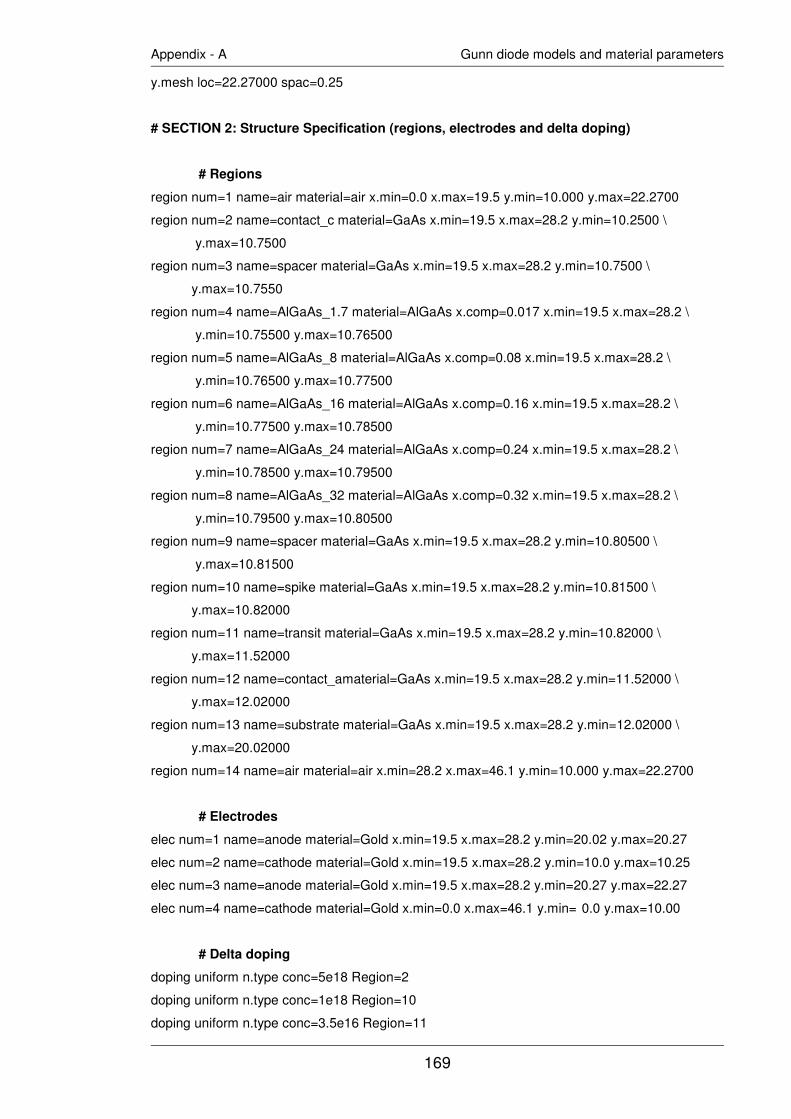
169
Appendix - A Gunn diode models and material parameters
y.mesh loc=22.27000 spac=0.25
# SECTION 2: Structure Specification (regions, electrodes and delta doping)
# Regions
region num=1 name=air material=air x.min=0.0 x.max=19.5 y.min=10.000 y.max=22.2700
region num=2 name=contact_c material=GaAs x.min=19.5 x.max=28.2 y.min=10.2500 \
y.max=10.7500
region num=3 name=spacer material=GaAs x.min=19.5 x.max=28.2 y.min=10.7500 \
y.max=10.7550
region num=4 name=AlGaAs_1.7 material=AlGaAs x.comp=0.017 x.min=19.5 x.max=28.2 \
y.min=10.75500 y.max=10.76500
region num=5 name=AlGaAs_8 material=AlGaAs x.comp=0.08 x.min=19.5 x.max=28.2 \
y.min=10.76500 y.max=10.77500
region num=6 name=AlGaAs_16 material=AlGaAs x.comp=0.16 x.min=19.5 x.max=28.2 \
y.min=10.77500 y.max=10.78500
region num=7 name=AlGaAs_24 material=AlGaAs x.comp=0.24 x.min=19.5 x.max=28.2 \
y.min=10.78500 y.max=10.79500
region num=8 name=AlGaAs_32 material=AlGaAs x.comp=0.32 x.min=19.5 x.max=28.2 \
y.min=10.79500 y.max=10.80500
region num=9 name=spacer material=GaAs x.min=19.5 x.max=28.2 y.min=10.80500 \
y.max=10.81500
region num=10 name=spike material=GaAs x.min=19.5 x.max=28.2 y.min=10.81500 \
y.max=10.82000
region num=11 name=transit material=GaAs x.min=19.5 x.max=28.2 y.min=10.82000 \
y.max=11.52000
region num=12 name=contact_amaterial=GaAs x.min=19.5 x.max=28.2 y.min=11.52000 \
y.max=12.02000
region num=13 name=substrate material=GaAs x.min=19.5 x.max=28.2 y.min=12.02000 \
y.max=20.02000
region num=14 name=air material=air x.min=28.2 x.max=46.1 y.min=10.000 y.max=22.2700
# Electrodes
elec num=1 name=anode material=Gold x.min=19.5 x.max=28.2 y.min=20.02 y.max=20.27
elec num=2 name=cathode material=Gold x.min=19.5 x.max=28.2 y.min=10.0 y.max=10.25
elec num=3 name=anode material=Gold x.min=19.5 x.max=28.2 y.min=20.27 y.max=22.27
elec num=4 name=cathode material=Gold x.min=0.0 x.max=46.1 y.min= 0.0 y.max=10.00
# Delta doping
doping uniform n.type conc=5e18 Region=2
doping uniform n.type conc=1e18 Region=10
doping uniform n.type conc=3.5e16 Region=11

170
Appendix - A Gunn diode models and material parameters
doping uniform n.type conc=5e18 Region=12
doping uniform n.type conc=2e18 Region=13
# SECTION 3: Material Parameters Definitions
# Regional and Band Parameters (band gap)
material name=AlGaAs_1.7 eg300=1.445199 permittivity=13.1507 nc300=6.83e17 \
nv300=1.30e19
material name=AlGaAs_8 eg300=1.52376 permittivity=12.968 nc300=1.60e18 nv300=1.33e19
material name=AlGaAs_16 eg300=1.62352 permittivity=12.736 nc300=2.77e18 nv300=1.37e19
material name=AlGaAs_24 eg300=1.72328 permittivity=12.504 nc300=3.93e18 nv300=1.41e19
material name=AlGaAs_32 eg300=1.82304 permittivity=12.272 nc300=5.10e18 nv300=1.46e19
# Recombination Parameters (SRH)
material name=AlGaAs_1.7 taun0=4.93e-9 taup0=2e-8 NSRHN=4.92e16 NSRHP=4.92e16
material name=AlGaAs_8 taun0=4.68e-9 taup0=2e-8 NSRHN=4.60e16 NSRHP=4.60e16
material name=AlGaAs_16 taun0=4.36e-9 taup0=2e-8 NSRHN=4.20e16 NSRHP=4.20e16
material name=AlGaAs_24 taun0=4.04e-9 taup0=2e-8 NSRHN=3.80e16 NSRHP=3.80e16
material name=AlGaAs_32 taun0=3.72e-9 taup0=2e-8 NSRHN=3.40e16 NSRHP=3.40e16
# Mobility Parameters (caughey Thomas)
mobility name=substrate mu1n.caug=800 alphan.caug=-0.9 betan.caug=-2.2 \
gamman.caug=-3.1 deltan.caug=0.5 ncritn.caug=1e17 mu2n.caug=2300
mobility name=Contact_A mu1n.caug=800 alphan.caug=-0.9 betan.caug=-2.2 \
gamman.caug=3.1 deltan.caug=0.5 ncritn.caug=1e17 mu2n.caug=1350
mobility name=Transit mu1n.caug=800 alphan.caug=-0.9 betan.caug=-2.2 \
gamman.caug=-3.1 deltan.caug=0.5 ncritn.caug=1e17 mu2n.caug=6300
mobility name=Spike mu1n.caug=800 alphan.caug=-0.9 betan.caug=-2.2 \
gamman.caug=-3.1 deltan.caug=0.5 ncritn.caug=1e17 mu2n.caug=2650
mobility name=Contact_C mu1n.caug=800 alphan.caug=-0.9 betan.caug=-2.2 \
gamman.caug=3.1 deltan.caug=0.5 ncritn.caug=1e17 mu2n.caug=1350
mobility material=GaAs betan=1
mobility material=AlGaAs gamman=2
#Giga – Self Heating Simulator Model Parameters
## k(T) = (tc.const) / [(T/300)]^tc.npow
material tcon.power
material f.tcond="$setpath/tcond.lib"
# C Interpreter Functions
material material=AlGaAs f.bandcomp="$setpath/bandcompAl.lib"

171
Appendix - A Gunn diode models and material parameters
material material=GaAs f.bandcomp="$setpath/bandcomp.lib"
material material=AlGaAs f.vsatn="$setpath/vsatn_7e6.lib"
material material=GaAs f.vsatn="$setpath/vsatn_7e6.lib"
mobility material=AlGaAs f.enmun="$setpath/enmun.lib"
material material=GaAs f.munsat="$setpath/munsat_GaAs.lib"
material material=AlGaAs f.munsat="$setpath/munsat.lib"
#Thermal Contacts for GIGATM
thermcontact number=1 name=Anode ext.temper=300
thermcontact number=2 name=Cathode ext.temper=300
# SECTION 3: Models Definitions
models material=GaAs consrh conmob analytic fldmob evsatmod=1 b.elec=2
models material=AlGaAs srh fldmob evsatmod=0 mobtem.simpl b.elec=2
models lat.temp joule.heat gr.heat
models material=AlGaAs cubic35
models hcte.el boltzmann temperature=300 print
# SECTION 4: Initial solution
# Method
method carriers=1 electrons
output e.field e.mobility e.temp e.velocity con.band val.band charge flowlines devdeg
method block newton itlimit=100 trap atrap=0.5 maxtrap=10 vsatmod.inc=0.001
# Contacts
contact all neutral
#contact name=anode neutral resistance=0.9 inductance=3.16e-12 capacitance=0.403e-12 \
# resonant
contact name=anode neutral resistance=0.9
contact name=cathode neutral
solve init
solve
save outfile=1898_P_0pt7Transit_298Ka.str
# SECTION 5a: DC I-V Simulations – Forward bias
log outf=1898_P_0pt7Transit_298K.log
solve vanode=0.0 vstep=0.1 vfinal=4.0 name=anode
save outfile=1898_P_0pt7Transit_Final_298K.str
log off
quit

172
Appendix - A Gunn diode models and material parameters
# SECTION 5b: DC I-V Simulations – Reverse bias
log outf=1898_N_0pt7Transit_298K.log
solve vanode=0.0 vstep=-0.1 vfinal=-4.0 name=anode
save outfile=1898_N_0pt7Transit_Final_298K.str
log off
quit
# SECTION 5c: Time Domain Simulations
solve init
save outfile=1898_ATLAST_HS.str
log outfile=1898_Trans_1_HS.log
solve vanode=2.5 ramptime=2.7e-11 tstop=2.7e-11 dt=1e-12
save outfile=1898_Trans_1_HS.str
# Extract I-V Characteristic above which the Negative Resistance begins
extract name="1898_Trans_HS.dat" curve(vint."anode", i."anode") outf="1898_Trans_HS.dat"
extract name="Icrit" max(i."anode")
extract name="UMax" max(vint."anode")
extract name="Ucrit" x.val from curve(vint."anode", i."anode") where y.val=$Icrit
extract name="Ecrit" $Ucrit/7e-5
# Time Domain Simulation at 2.5V Constant External Bias
log outfile=1898_Trans_2_HS.log
solve tstop=12e-11 dt=2e-11 outfile=1898_Trans_2_x0 master
log off
extract the oscillation frequency by measuring the time for 4 periods
extract init inf="1898_Trans_2_HS.log"
extract name="v_ave" ave(vint."anode")
extract name="t1" x.val from curve(time, vint."anode") where y.val=$"v_ave"
extract name="t2" x.val from curve(time, vint."anode") where y.val=$"v_ave" and val.occno=7
extract name="delta" ($"t2" - $"t1") / 3
extract name="f@2pt5V" 1 / $"delta"
# Ramp-up to 3.0 V External Bias
load inf=1898_Trans_1_HS.str master
solve previous
solve vanode=3 ramptime=2.7e-11 tstop=2.7e-11 dt=1e-12

173
Appendix - A Gunn diode models and material parameters
save outfile=1898_Trans_3_HS.str
# Time Domain Simulation at 3.0V Constant External Bias
log outfile=1898_Trans_3_HS.log
solve tstop=12e-11 dt=2e-11 outfile=1898_Trans_3_x0 master
log off
extract init inf="1898_Trans_3_HS.log"
extract name="v_ave" ave(vint."anode")
extract name="t1" x.val from curve(time,vint."anode") where y.val=$"v_ave"
extract name="t2" x.val from curve(time,vint."anode") where y.val=$"v_ave" and val.occno=7
extract name="delta" ($"t2" - $"t1") / 3
extract name="f@3V" 1 / $"delta"
quit

Appendix – B
Schottky Diode – SILVACOTM code SILVACO
TM code for a 14µm diameter Schottky diode is presented. The statements with hash
(#) are the remarks which are ignored during simulation code execution. A line continuation
operator ‘\’ shows that code continues in the next line. The C-Interpreter file path is arbitrary..
SILVACOTM
DeckBuildTM
code
go atlas
title "Schottky 4 multipliers 14um diameter"
# SECTION 1: Mesh input
mesh width = 120 auto
x.mesh loc=0.0 spac=0.5
x.mesh loc=1.5 spac=0.5
x.mesh loc=2.0 spac=0.25
x.mesh loc=2.5 spac=0.5
x.mesh loc=2.994 spac=0.01
x.mesh loc=2.995 spac=0.01
x.mesh loc=3.0 spac=0.01
x.mesh loc=3.5 spac=0.25
x.mesh loc=5.25 spac=0.15
y.mesh loc=-0.0605 spac=0.1
y.mesh loc=-0.033 spac=0.001
y.mesh loc=0.0 spac=0.001
y.mesh loc=0.35 spac=0.01
y.mesh loc=3.35 spac=0.2
y.mesh loc=6.35 spac=1.2
y.mesh loc=14.35 spac=2.0
# SECTION 2: Structure Specification (regions, electrodes and delta doping)
# Regions
region num=1 name="Cap" material=InGaAs y.min=-0.0605 y.max=-0.033 x.comp=0.2
166 174
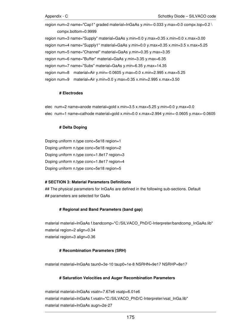
175
Appendix - C Schottky Diode – SILVACO code
region num=2 name="Cap1" graded material=InGaAs y.min=-0.033 y.max=0.0 compx.top=0.2 \
compx.bottom=0.9999
region num=3 name="Supply" material=GaAs y.min=0.0 y.max=0.35 x.min=0.0 x.max=3.00
region num=4 name="Supply1" material=GaAs y.min=0.0 y.max=0.35 x.min=3.5 x.max=5.25
region num=5 name="Channel" material=GaAs y.min=0.35 y.max=3.35
region num=6 name="Buffer" material=GaAs y.min=3.35 y.max=6.35
region num=7 name="Subs" material=GaAs y.min=6.35 y.max=14.35
region num=8 material=Air y.min=-0.0605 y.max=0.0 x.min=2.995 x.max=5.25
region num=9 material=Air y.min=0.0 y.max=0.35 x.min=2.995 x.max=3.50
# Electrodes
elec num=2 name=anode material=gold x.min=3.5 x.max=5.25 y.min=0.0 y.max=0.0
elec num=1 name=cathode material=gold x.min=0.0 x.max=2.994 y.min=-0.0605 y.max=-0.0605
# Delta Doping
Doping uniform n.type conc=5e18 region=1
Doping uniform n.type conc=5e18 region=2
Doping uniform n.type conc=1.8e17 region=3
Doping uniform n.type conc=1.8e17 region=4
Doping uniform n.type conc=5e18 region=5
# SECTION 3: Material Parameters Definitions
## The physical parameters for InGaAs are defined in the following sub-sections. Default
## parameters are selected for GaAs
# Regional and Band Parameters (band gap)
material material=InGaAs f.bandcomp="C:/SILVACO_PhD/C-Interpreter/bandcomp_InGaAs.lib"
material region=2 align=0.34
material region=3 align=0.36
# Recombination Parameters (SRH)
material material=InGaAs taun0=3e-10 taup0=1e-8 NSRHN=9e17 NSRHP=8e17
# Saturation Velocities and Auger Recombination Parameters
material material=InGaAs vsatn=7.67e6 vsatp=6.01e6
material material=InGaAs f.vsatn="C:/SILVACO_PhD/C-Interpreter/vsat_InGa.lib"
material material=InGaAs augn=2e-27

176
Appendix - C Schottky Diode – SILVACO code
# Mobility Parameters (caughey Thomas)
mobility material=InGaAs mu1n.caug=2000 mu2n.caug=12000 mu1p.caug=050 mu2p.caug=400\
ncritn.caug=6.4e17 ncritp.caug=7.4e17
mobility material=InGaAs alphan.caug=0 alphap.caug=0 betan.caug=0 betap.caug=0 \
gamman.caug=0 gammap.caug=0 deltan.caug=0 deltap.caug=0
mobility material=InGaAs f.enmun="C:/SILVACO_PhD/C-Interpreter/enmun_In.lib"
material material=InGaAs f.munsat="C:/SILVACO_PhD/C-Interpreter/munsat_In.lib"
# SECTION 3: Models Definitions
models fldmob auger consrh fermidirac temperature=300 print
# SECTION 4: Initial Solution
output e.field e.mobility e.temp e.velocity con.band val.band charge flowlines
# Contacts
contact name=anode workfunc=4.815
contact name=cathode
method block newton itlimit=100 trap atrap=0.5 maxtrap=10 vsatmod.inc=0.001
solve init
save outf=Schottky_Ohmic-Cap_Rev-14um-DIA.str
# SECTION 4: AC solution for plotting a C-V curve
solve vanode=0
log outf=AC_Schottky_14um-DIA.log s.param inport=anode outport=anode y.param
solve vanode=0.0 vstep=-0.05 vfinal=-10.0 name=anode ac freq=1e9 fstep=10e9 nfsteps=9
save outf=AC_Schottky_Ohmic-ve14um-DIA.str
logoff
tonyplot AC_Schottky_14um-DIA.log
quit

Appendix – C
Dipole Domain Formation
1. One dipole formation showing the transit region electron concentration, zoomed between 16.4 and 16.9 cm-3.
2. Two dipoles showing the transit region electron concentration, zoomed between 16.4 and 16.9 cm-3.
Ele
ctr
on C
oncen
tra
tion
cm
-3
31
0601
36
177
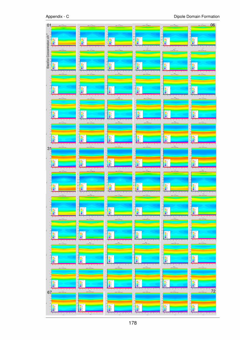
178
Appendix - C Dipole Domain Formation
Ele
ctr
on C
oncen
tra
tion
cm
-3
31
0601
7267

References
1. Sze, S.M., High Speed Devices. 1990: New York ; Chichester : Wiley. 2. Hobson, G.S., The Gunn effect. 1974. Oxford : Clarendon Press. 3. Sze, S.M., Semiconductor Devices Physics and Technology. 2nd edition
2002, New York: NY Willey. 4. Montanari, S., Fabrication and Characterization of planar Gunn Diodes for
Monolithic Microwave Integrated Circuits, in RWTH. 2005, University of Aachen.
5. Townsend, S.M., AlGaAs/GaAs Graded Gap Gunn Diodes for Autonomous Intelligent Cruise Control Radar Applications, in EEE, M&N Group. 1999, UMIST: Manchester.
6. Gallerano, G.P. Overview of Terahertz Radiation Sources. in Proceedings of the 2004 FEL Conference. 2004.
7. Electronic Warfare and Radar Systems Engineering Handbook. 2 ed. 1997, Washington, D.C. 20361: Avionics Department. 1-298.
8. Shur, M. Terahertz technology: Devices and applications. in Proceedings of ESSDERC 2005: 35th European Solid-State Device Research Conference. 2005.
9. Tait, G.B. and Krowne, C.M., Efficient transferred electron device simulation method for microwave and millimeter wave cad applications. Solid-State Electronics, 1987. 30(10): p. 1025-1036.
10. Forster, A.A., Hot electron injector Gunn diode for advanced driver assistance systems. Applied physics. A, Materials science & processing, 2007. 87(3): p. 545-58.
11. Montanari, S.S., High frequency investigation of graded gap injectors for GaAs Gunn diodes. Solid-state electronics, 2005. 49(2): p. 245-50.
12. Couch, N.N.R., High-performance, graded AlGaAs injector, GaAs Gunn diodes at 94 GHz. IEEE electron device letters, 1989. 10(7): p. 288-90.
13. N. Farrington, Carr, M., Sly, J. L., and Missous, M., Development of an on-wafer test for rapid evaluation of doping spike carrier concentration levels in commercially manufactured GaAs Gunn diodes for automotive radar applications. in Interational Conferance on Compound Semiconductor Manufacturing Technology (CSManTech’08). 2008. Chicago, USA.
14. Phillips, T.T.G., Submillimeter astronomy [heterodyne spectroscopy]. Proceedings of the IEEE, 1992. 80(11): p. 1662-78.
15. Tonouchi, M., Cutting-edge terahertz technology, in Nat Photon. 2007. p. 97-105.
16. Siegel, P.H., Terahertz technology. IEEE transactions on microwave theory and techniques, 2002. 50(3): p. 910-28.
17. Siegel, P.H. THz applications for outer and inner space. in 17th International Zurich Symposium on Electromagnetic Compatibility. 2006.
18. Carr, G., et al., High-power terahertz radiation from relativistic electrons. Nature, 2002. 420(6912): p. 153-156.
19. Anwar, A. Staying the course in the GaAs industry. in International Conference on Compound Semiconductor Manufacturing Technology. 2005.
179

180
References
20. Gunn, J., Microwave Oscillations of Current in III-V Semiconductors. Solid State Communications, 1963. 1(4): p. 88-91.
21. Esaki, L., New Phenomenon in Narrow Germanium p-n Junctions. Physical Review, 1958. 109(2): p. 603.
22. Chang, L., Esaki L., and Tsu, R., Resonant Tunneling in Semiconductor Double Barriers. Applied physics letters, 1974. 24(12): p. 593-595.
23. Read, W., A proposed high-frequency, negative-resistance diode. The Bell system technical journal, 1958. 37(2): p. 401-446.
24. Ruegg, H.W., A proposed punch-through microwave negative-resistance diode. Electron Devices, IEEE Transactions on, 1968. 15(8): p. 577-585.
25. Okabe, T., et al., Bulk oscillation by tunnel injection. Electron Devices, IEEE Transactions on, 1969. 16(2): p. 251-251.
26. Elta, M.E. and Haddad, G.I., High-Frequency Limitations of IMPATT, MITATT, and TUNNETT Mode Devices. Microwave Theory and Techniques, IEEE Transactions on, 1979. 27(5): p. 442-449.
27. Elta, M.E. and Haddad, G.I., Large-signal performance of microwave transit-time devices in mixed tunneling and avalanche breakdown. Electron Devices, IEEE Transactions on, 1979. 26(6): p. 941-948.
28. Gunn, J.J.B., Microwave oscillations of current in III-V semiconductors. Solid State Communications, 1993. 88(11): p. 883-886.
29. Streetman, B.G., Solid state electronic devices. 4th ed. Prentice Hall series in solid state physical electronics. 1995: Englewood Cliffs, N.J. : Prentice Hall, c1995.
30. Townsend, S. Low resistance ohmic contacts to millimetre-wave graded gap Gunn diode oscillators. in Workshop on High Performance Electron Devices for Microwave and Optoelectronic Applications, EDMO. 1997.
31. e2v Technologies Plc, DC1279F-T 76–78GHz Gunn Diode Data sheet. 32. Brown, E. R., Soderstrom, J. R., Parker, C. D., Mahoney, L. J., Molvar, K.
M. and McGill, T. C., Oscillations up to 712 GHz in InAs/AlSb resonant tunneling diodes. Applied Physics Letters, 1991. 58(20): p. 2291-2293.
33. Suzuki, S., Teranishi, A., Hinata, K., Asada, M., Sugiyama, H. and Yokoyama, H., Fundamental oscillation up TO 831 GHz in GaInAs/AlAs resonant tunneling diode. in IEEE International Conference on Indium Phosphide & Related Materials, 2009. IPRM '09. . 2009.
34. Sze, S.M. and Kwok K. Ng, Physics of semiconductor devices. 3rd ed. 2006, New York: Wiley-Blackwell.
35. Jun-ichi, N, Plotka, P., Makabe, H. and Kurabayashi, T., GaAs TUNNETT diodes oscillating at 430-655 GHz in CW fundamental mode. Microwave and Wireless Components Letters, IEEE, 2005. 15(9): p. 597-599.
36. Elta, M., Fetterman, H., Macropoulos, W. and Lambert, J., 150 GHZ GAAS MITATT SOURCE. Electron device letters, 1980. 1(6): p. 115-116.
37. Robert LaGuerra, D.F., Ed Rerisi, ABI (Automotive Radar/Lidar Systems) A component level market analysis of radar, lidar, ultrasonic, and optics-based automotive safety systems 2004.
38. Pilgrim, N., Macpherson, R., Khalid, A., Dunn, G. and Cumming, D., Multiple and broad frequency response Gunn diodes. Semiconductor science and technology, 2009. 24(10): p. 105010.
39. Pilgrim, N. J., Khalid, A., Li, C., Dunn, G. M. and Cumming, D. R. S., Contact shaping in planar Gunn diodes. physica status solidi (c), 2010. 8(2): p. 313-315.

181
References
40. Perez, S., Gonzalez, T., Pardo, D. and Mateos, Terahertz gunn-like oscillations in InGaAs/InAlAs planar diodes. Journal of applied physics, 2008. 103(9): p. 094516.
41. Huang, J., Yang, H., Tian, C., Dong, J., Zhang, H. and Guo, T., Design and manufacture of planar GaAs Gunn diode for millimeter wave application. Chinese Physics B, 2010. 19(12): p. 127203.
42. Li, C., Khalid, A., Pilgrim, N., Holland, M., Dunn, G. and Cumming, D., Novel Planar Gunn Diode Operating in Fundamental Mode up to 158 GHz. Journal of physics. Conference series, 2009. 193: p. 012029.
43. Crowe, T.T.W., Terahertz GaAs devices and circuits for heterodyne receiver applications. International journal of high speed electronics, 1995. 6(1): p. 125-61.
44. Zhong, H. Inspection of Space Shuttle Insulation Foam Defects Using a 0.2 THz Gunn Diode Oscillator. in IEEE conference Digest of the 2004 Joint 29th International Conference on Infrared and Millimeter Waves and 12th International Conference on Terahertz Electronics. 2004.
45. Federici, J.J.F., THz imaging and sensing for security applications-explosives, weapons and drugs. Semiconductor Science and Technology, 2005. 20(7): p. S266-80.
46. Leahy-Hoppa, M.M.R., Wideband terahertz spectroscopy of explosives. Chemical Physics Letters, 2007. 434(4): p. 227-30.
47. Frost and Sullivan, The Market for Obstacle Sensing Technologies in Passenger Cars and Commercial Vehicles in Europe. 2005.
48. Khlopov, G. and Schuenemann, K., Application of Millimetre Wave Coherent Radar for Remote Measurement of Vibrations and Displacements. in Conference Digest of the 2004 Joint 29th International Conference on Infrared and Millimeter Waves and 12th International Conference on Terahertz Electronics 2004: IEEE.
49. Barth, H. and Menzel, W., GaAs Gunn Oscillators Reach the 140 GHz Range. in Microwave Symposium Digest, 1985 IEEE MTT-S International. 1985.
50. Neylon, S.S., State-of-the-art performance millimetre wave gallium arsenide Gunn diodes using ballistically hot electron injectors. IEEE MTT-S International Microwave Symposium Digest, 1989. 1: p. 519-522.
51. Beton, P.P.H., Use of n<sup>+</sup> spike doping regions as nonequilibrium connectors. Electronics letters, 1988. 24(7): p. 434-435.
52. Kiuru, T., et al. Gunn oscillator modeling and second harmonic output power optimization at 76 GHz. in Microwave Symposium Digest, 2008 IEEE MTT-S International. 2008.
53. Carlstrom, J.E., Plambeck, R.L., and D.D. Thornton, A Continuously Tunable 65--15-GHz Gunn Oscillator. Microwave Theory and Techniques, IEEE Transactions on, 1985. 33(7): p. 610-619.
54. Jones, S. H., Zybura, M. F., Carlstrom, J. E. and O'Brien, T. M., A 63-170 GHz second-harmonic operation of an InP transferred electron device. Electron Devices, IEEE Transactions on, 1999. 46(1): p. 17-23.
55. Van Zyl, R., Perold, W., and Botha, R.. The Gunn-diode: fundamentals and fabrication. in Communications and Signal Processing, 1998. COMSIG '98. Proceedings of the 1998 South African Symposium on. 1998.
56. Bullman, J., Hobson, G.S, and Taylor, B.C., The Gunn-Hilsum Effect. 1979, New York: Academic Press Inc.

182
References
57. Wang, B., AbouElnour, A., and Schunemann, K., Determination of the influence of doping profile on the performance of mm-wave gunn elements by using an efficient physical simulator. International journal of infrared and millimeter waves, 1996. 17(7): p. 1205-1218.
58. Butcher, P.P.N., Theory of stable domain propagation in the Gunn effect. Physics letters, 1965. 19(7): p. 546-547.
59. Dunn, G. and Kearney M., A theoretical study of differing active region doping profiles for W-band (75-110 GHz) InP Gunn diodes. Semiconductor science and technology, 2003. 18(8): p. 794-802.
60. Teoh, Y., Dunn, G., Priestley, N. and Carr, M., Monte Carlo simulations of asymmetry multiple transit region Gunn diodes. Semiconductor science and technology, 2005. 20(5): p. 418-422.
61. Kamoua, R. and Eisele H., Theoretical and experimental comparison of optimized doping profiles for high-performance InP Gunn devices at 220-500 GHz, in 2003 Ieee Mtt-S International Microwave Symposium Digest, Vols 1-3, H. Thal, Editor. 2003, Ieee: New York. p. 907-910.
62. Pilgrim, N., Khalid, A., Dunn, G. and Cumming, D., Gunn oscillations in planar heterostructure diodes. Semiconductor science and technology, 2008. 23(7): p. 075013.
63. Bosch, B.G. and Engel, R.W.H., Gunn-effect electronics. 1975: London (etc.) : Pitman.
64. Bulman, P.J., Transferred electron devices 1972: New York ; London : Academic Press.
65. Navon, D.H., Semiconductor Microwave and Materials. 1987: HRW Int. Edition.
66. Li, S.S., Semiconductor physical electronics. Microdevices. 1993 New York : Plenum.
67. Couch, N.N.R., Hot electron injection in millimetre wave Gunn diodes. Solid-state electronics, 1989. 32(12): p. 1685-8.
68. Ruch, J.J.G., Temperature dependence of the transport properties of gallium arsenide determined by a Monte Carlo method. Journal of applied physics, 1970. 41(9): p. 3843-9.
69. Couch, N.N.R., The use of linearly graded composition AlGaAs injectors for intervalley transfer in GaAs: theory and experiment. Solid-state electronics, 1988. 31(3): p. 613-16.
70. Lee, C.C., Monte Carlo comparison of heterojunction cathode Gunn oscillators. Electronics letters, 1990. 26(7): p. 425-7.
71. Copeland, J.J.A., A new mode of operation for bulk negative resistance oscillators. Proceedings of the IEEE, 1966. 54(10): p. 1479-1480.
72. Copeland, J.J.A., Characterization of bulk negative-resistance diode behavior. IEEE transactions on electron devices, 1967. 14(9): p. 461-463.
73. Copeland, J., LSA Oscillator-Diode Theory. Journal of applied physics, 1967. 38(8): p. 3096.
74. Harrison, W.W.A., Universal linear-combination-of-atomic-orbitals parameters for d-state solids. Physical review. B, Condensed matter, 1980. 21(8): p. 3214-21.
75. Greenwald, Z.Z., The effect of a high energy injection on the performance of mm wave Gunn oscillators. Solid-state electronics, 1988. 31(7): p. 1211-14.
76. Missous, M., Conduction and Valence Band Offsets at the AlGaAs/GaAs heterostructure interface. Properties of Aliminium Galium Aesenide, ed. S. Adachi. 1991: IEE INSPEC. 325.

183
References
77. Missous, M., In situ, near-ideal epitaxial AlxGa1-xAs Schottky barriers formed by molecular beam epitaxy. Journal of applied physics, 1990. 68(5): p. 2239-45.
78. Vurgaftman, I.I., Band parameters for III-V compound semiconductors and their alloys. Journal of applied physics, 2001. 89(11): p. 5815-75.
79. Stock, J., Herstellung und Charakterisierung von GaAs Gunn-Dioden für Anwendungen bei 77GHz. 2003, University of Aachen RWTH Aachen.
80. VWF Interactive Tools, Device Simulation Software. Vol. CA 95054. 2005, Santa Clara: SILVACO International.
81. Atlas User’s Manual, Device Simulation Software. Vol. Version 5.10.R,. 2005, Santa Clara: SILVACO International.
82. DevEdit, User’s Manual. 2006, Santa Clara, CA 95054: SILVACO International.
83. DeckBuild, User’s Manual. Vol. Version 3.26.R. 2005, Santa Clara, CA 95054: SILVACO International.
84. TonyPlot, User’s Manual. Vol. Version 3.4.0.R. 2006, Santa Clara, CA 95054: SILVACO International.
85. Palankovski, V. and Quay, R., Analysis and simulation of heterostructure devices. 2004, Wien, Austria: Springer.
86. Palankovski, V., Schultheis, R., and Selberherr, S., Simulation of power heterojunction bipolar transistors on gallium arsenide. Electron Devices, IEEE Transactions on, 2001. 48(6): p. 1264-1269.
87. Caughey, D.M., Carrier mobilities in silicon empirically related to doping and field. Proceedings of the IEEE, 1967. 55(12): p. 2192-2193.
88. Barnes, J.J.J., Finite-element simulation of GaAs MESFET's with laterall doping profiles and submicron gates. IEEE transactions on electron devices, 1976. 23(9): p. 1042-1048.
89. Shockley, W.W., Statistics of the recombinations of holes and electrons. Physical review, 1952. 87: p. 835-842.
90. Hall, R.R.N., Electron-hole recombination in germanium. Physical review, 1952. 87: p. 387-387.
91. Wachutka, G.G.K., Rigorous thermodynamic treatment of heat generation and conduction in semiconductor device modeling. IEEE transactions on computer-aided design of integrated circuits and systems, 1990. 9(11): p. 1141-9.
92. Farahmand, M., Monte Carlo simulation of electron transport in the III-nitride wurtzite phase materials system: Binaries and ternaries. IEEE transactions on electron devices, 2001. 48(3): p. 535-542.
93. Stratton, R., Semiconductor current-flow equations (diffusion and degeneracy). Electron Devices, IEEE Transactions on, 1972. 19(12): p. 1288-1292.
94. Stratton, R., Diffusion of Hot and Cold Electrons in Semiconductor Barriers. Physical Review, 1962. 126(6): p. 2002.
95. Meinerzhagen, B., Bach, K. H., Bork, I. and Eng, W. L., A New Highly Efficient Nonlinear Relaxation Scheme for Hydrodynamic MOS Simulations. in Numerical Modeling of Processes and Devices for Integrated Circuits, 1992. NUPAD IV. Workshop on. 1992.
96. Apanovich, Y., et al., Numerical simulation of submicrometer devices including coupled nonlocal transport and nonisothermal effects. Electron Devices, IEEE Transactions on, 1995. 42(5): p. 890-898.
97. Apanovich, Y., Blakey, P., Cottle, R., Lyumkis, E., Polsky, B., Shur, A. and Tcherniaev, A., Steady-state and transient analysis of submicron devices

184
References
using energy balance and simplified hydrodynamic models. Computer-Aided Design of Integrated Circuits and Systems, IEEE Transactions on, 1994. 13(6): p. 702-711.
98. Manual, S.I.A.U.s., Device Simulation Software. Vol. Software version 5.16.3.R. 2010, Santa Clara, CA 95054: SILVACO International.
99. Amir, F., Farrington, N., Tauqeer, T. and Missous, M., Physical Modelling of a Step-Graded AlGaAs/GaAs Gunn Diode and Investigation of Hot Electron Injector Performance. in Advanced Semiconductor Devices and Microsystems, 2008. ASDAM 2008. International Conference on. 2008.
100. Amir, F., Farrington, N., Tauqeer, T. and Missous, M., Development of a novel 3D physical model of an advanced mm-wave Gunn diode with hot-electron injection, in 17th European Heterostructure Technology Workshop, HETECH 2008 2008: Venice, Italy.
101. Amir, F., Mitchell, C., Farrington, N. and Missous, M., Advanced Gunn Diode as High Power Terahertz Source for a Millimetre Wave High Power Multiplier. in SPIE Europe Security + Defence 2009. 2009. Berliner Congress Centre, Berlin, Germany, Berlin Germany: SPIE.
102. Amir, F., Farrington, N., Mitchell, C. and Missous, M., Time-domain analysis of sub-micron transit region GaAs Gunn diodes for use in terahertz frequency multiplication chains. in SPIE Europe Security + Defence 2010, SD108 ‘Millimetre Wave and Terahertz Sensors and Technology. 2010. Centre de Congrès Pierre Baudis, Toulouse, France: SPIE.
103. Farrington, N. Norton, P., Carr, M., Sly, J. and Missous, M., A ruggedly packaged D-Band GaAs Gunn diode with hot electron injection suitable for volume manufacture. IEEE MTT-S International Microwave Symposium digest, 2008. 1-4: p. 282-285.
104. Amir, F., Mitchell, C. and Missous, M., Development of advanced Gunn diodes and Schottky multipliers for high power THz sources, in 8th International Conference on Advanced Semiconductor Devices & Microsystems (ASDAM 2010), 2010.


![Review of Terahertz Tomography Techniques - Inria · PDF fileReview of Terahertz Tomography Techniques ... Gunn diode [73], plasma wave transistor [74, 75], Backward Wave Oscillator](https://img.dokumen.tips/doc/110x75/5ab01d3a7f8b9a3a038e439b/review-of-terahertz-tomography-techniques-inria-of-terahertz-tomography-techniques.jpg)