Embed Size (px)
Citation preview
Advanced light source technologies that enable high-volume manufacturing of DUV lithography extensions
Theodore Cacouris, Rajasekhar Rao, Rostislav Rokitski, Rui Jiang, John Melchior, Bernd Burfeindt,
Kevin O'Brien, Cymer Inc., 17075 Thornmint Court, San Diego, CA, 92127, USA
1. INTRODUCTION Extending DUV lithography with double patterning (DP) has gained widespread use at the 32nm technology node. The lithography community has converged now on extending the use of immersion DP lithography to the 22nm node. Since DP involves exposing critical layers twice in order to achieve the necessary feature resolution, it has an adverse impact on the lithography tool productivity. In order to support productivity improvements and the resulting tighter requirements for CD uniformity and overlay for immersion DP lithography, stringent demands are placed on the light source performance. We introduced the XLRTM 600ix in 2010 at various chipmaker locations and reported on the capability of this light source to operate in the challenging environment presented by immersion DP lithography.1 Various technology advancements were introduced and the results of the reliability testing were presented.1 In this paper, the performance of the light source in the field is presented, demonstrating the stable and reliable performance. We have continued to further improve on the reliability, tool availability and performance flexibility of our DUV light sources by developing and implementing newer technology advancements. Specifically, improvements in the discharge chamber gas control and the capability to operate over a wide range of spectral bandwidths were developed. Improved gas control extends gas life thereby improving light source availability. The capability to operate over a wide range of spectral bandwidths for the purposes of increasing depth of focus (DOF) is known as focus drilling, which supports up to 2X improvement in the DOF at the wafer for critical contact and via layers. In this paper, the key elements of these technology advancements are described.
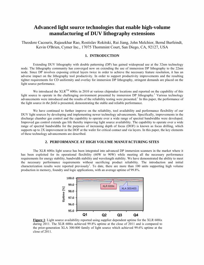
2. PERFORMANCE AT HIGH VOLUME MANUFACTURING SITES The XLR 600ix light source has been integrated into advanced DP immersion scanners in the market where it has been exploited for its operational flexibility (60W to 90W) while meeting all the necessary performance requirements for energy stability, bandwidth stability and wavelength stability. We have demonstrated the ability to meet the necessary performance requirements without sacrificing product reliability. The introduction and initial characterization results were reported previously1. To date, there are more than 100 units supporting high volume production in memory, foundry and logic applications, with an average uptime of 99.8%.
Figure 1: Light source availability reported using supplier dependent uptime for the XLR 600ix during 2011. The XLR 600ix achieved 99.8% uptime at the close of 2011 and is compared to the prior-generation XLA 300/400 family of light source which achieved 99.6% uptime at the close of 2011.

The flexibility to operate over a range of output power from 60W to 90W subjects the light source to stringent performance requirements. For example, operation at 90W requires fewer pulses to achieve the same dose exposure when compared to operating at 60W. The challenging operational condition then for the light source is at 90W output power and at the reduced exposure window sizes. In order to achieve improved dose stability, further refinements were developed in the pulse-to-pulse energy control algorithms that include feed-forward and feedback control. The resultant field performance of the light source at a memory chipmaker fab is shown in figures 2 through 4. The light source was operated at 90W for over a year and has demonstrated stable and predictable performance under such challenging conditions.
Figure 2: Maximum dose error measured on a light source in 90W operation at a memory fab. Performance is stable and functioning within 0.05% throughout its operation.
Figure 3: Maximum wavelength error measured on a light source in 90W operation at a memory fab. Performance is stable and functioning within less than 5fm throughout its operation
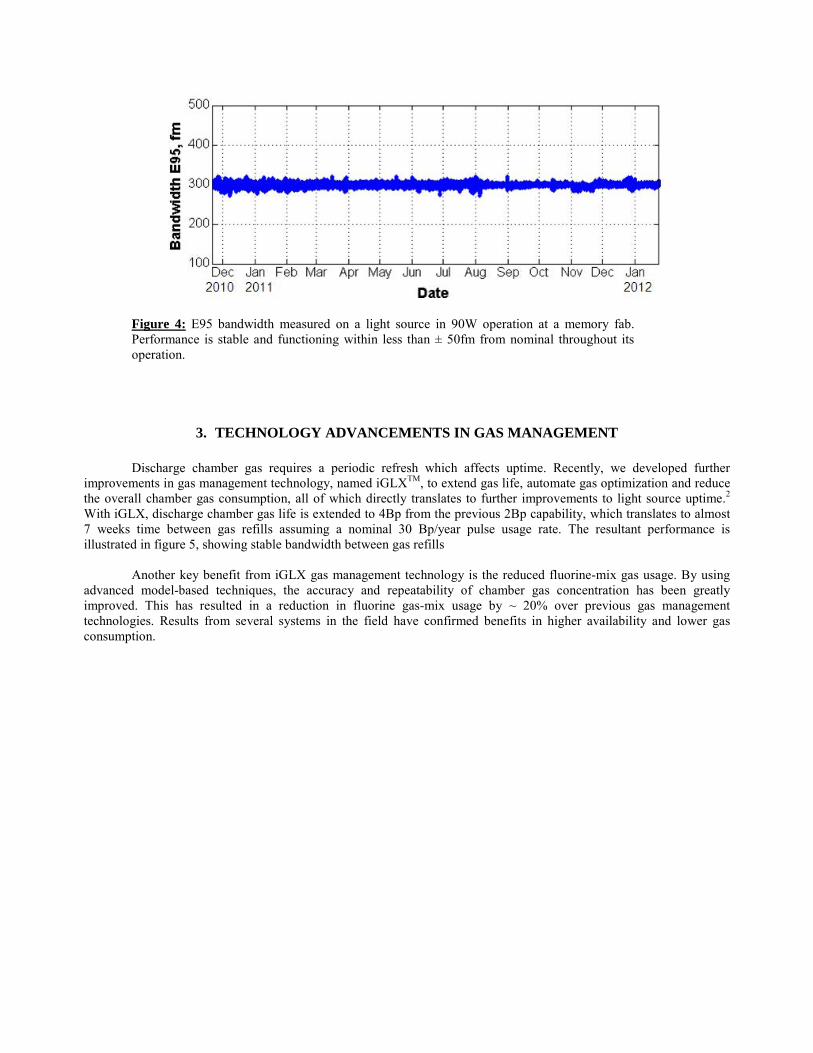
Figure 4: E95 bandwidth measured on a light source in 90W operation at a memory fab. Performance is stable and functioning within less than ± 50fm from nominal throughout its operation.
3. TECHNOLOGY ADVANCEMENTS IN GAS MANAGEMENT Discharge chamber gas requires a periodic refresh which affects uptime. Recently, we developed further improvements in gas management technology, named iGLXTM, to extend gas life, automate gas optimization and reduce the overall chamber gas consumption, all of which directly translates to further improvements to light source uptime. 2 With iGLX, discharge chamber gas life is extended to 4Bp from the previous 2Bp capability, which translates to almost 7 weeks time between gas refills assuming a nominal 30 Bp/year pulse usage rate. The resultant performance is illustrated in figure 5, showing stable bandwidth between gas refills
Another key benefit from iGLX gas management technology is the reduced fluorine-mix gas usage. By using advanced model-based techniques, the accuracy and repeatability of chamber gas concentration has been greatly improved. This has resulted in a reduction in fluorine gas-mix usage by ~ 20% over previous gas management technologies. Results from several systems in the field have confirmed benefits in higher availability and lower gas consumption.

Figure 5: Bandwidth stability during an extended period between gas refills, illustrating iGLX can maintain stable performance with greater than 4Bp between refills. The top data represents E95 bandwidth, while the lower data represents full width half-maximum (FWHM) bandwidth. The vertical bar shows the refill events.
4. TECHNOLOGY ADVANCEMENTS WITH FOCUS DRILLING Light sources used in advanced photolithography usually require a light source with narrow spectral bandwidth to support achieving the necessary CD uniformity. However, this also limits the process window available to chipmakers in high N.A. systems where the depth of focus (DoF) is small. The challenge for contact layers in particular is the decreasing process window area with reducing feature sizes. We have developed focus drilling technology to support a larger process window in the patterning of contact and via layers. 3 The goal is to increase DoF without a significantly adverse impact on critical process parameters like CD uniformity, mask error enhancement factor (MEEF) or exposure latitude (EL). This is enabled by providing a light source with the capability to broaden the spectral bandwidth to suit a specific chipmaker process. The focus drilling feature provides such a broad spectral bandwidth tuning capability along with the necessary supporting metrology and control capability and thereby providing increased process latitude to chipmakers. 3 We have investigated many novel methods of spectral tuning. 4 Once such embodiment has been integrated into the light source to support three key elements that are needed to support the focus drilling feature. The key elements are bandwidth actuation (tuning), spectral metrology and a control scheme. Novel improvements have been integrated into the line narrowing module (LNM) to provide a wide spectral bandwidth tuning range. This is essential to providing the increased DoF and its associated process latitude. Separately, advanced metrology methods have been incorporated into the bandwidth analysis module (BAM) to support accurate spectral measurements over the wide tuning range. Accurate bandwidth metrology supports chipmaker process repeatability. The spectral bandwidth tuning range that is available with the new LNM is shown in figure 6 below. Using spectral E95 as the metric, the tuning range that is available with focus drilling is increased to up to 1.8pm. This is supported with advanced bandwidth metrology that can accurately measure various spectral parameters like FWHM, E95 or any other derived spectral metric.
0 1 2 3 4 5 6 7 Pulses (x10
9)
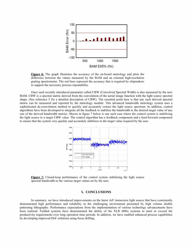
Figure 6: The graph illustrates the accuracy of the on-board metrology and plots the difference between the values measured by the BAM and an external high-resolution grating spectrometer. The red lines represent the accuracy that is required by chipmakers to support the necessary process repeatability.
Once such recently introduced parameter called CBW (Convolved Spectral Width) is also measured by the new BAM. CBW is a spectral metric derived from the convolution of the aerial image function with the light source spectral shape. (See reference 5 for a detailed description of CBW). The essential point here is that any such derived spectral metric can be measured and reported by the metrology module. This advanced bandwidth metrology system uses a sophisticated de-convolution method to quickly and accurately extract the light source spectrum. In addition, control algorithms have been developed to integrate all the feedback to stabilize the bandwidth to the desired target value of any one of the derived bandwidth metrics. Shown in figure 7 below is one such case where the control system is stabilizing the light source to a target CBW value. The control algorithm has a feedback component and a feed-forward component to ensure that the system very quickly and accurately stabilizes to the target value required by the user.
Figure 7: Closed-loop performance of the control system stabilizing the light source spectral bandwidth to the various target values set by the user.
5. CONCLUSIONS In summary, we have introduced improvements on the latest ArF immersion light source that have consistently demonstrated high performance and reliability in the challenging environment presented by high volume double patterning lithography. Performance expectations from the implementation of various technology advancements have been realized. Fielded systems have demonstrated the ability of the XLR 600ix systems to meet or exceed the productivity requirements over long operation time periods. In addition, we have enabled enhanced process capabilities by developing improved DoF solutions using focus drilling.

6. REFERENCES 1. Rostislav Rokistki, Toshi Ishihara, Rajasekhar Rao, Rui Jiang, Mary Haviland, Theodore Cacouris, Daniel Brown
“High Reliability ArF Light Source for Double Patterning Immersion Lithography”, Optical Microlithography XXIII, Proc of SPIE 2010 Vol 7640.
2. Daniel J. Riggs, Kevin O’Brien, Daniel Brown, “DUV Light Source Availability Improvement via Further Enhancement of Gas Management Technologies”, Optical Microlithography XXIV, Proc of SPIE 2011, to be published.
3. Ivan Lalovic, Jason Lee, Nakgeoun Seong, Nigel Farrar, Michiel Kupers, Hans van der Laan, Tom van der Hoeff, Carsten Kohler, “Focus Drilling for Increased Process Latitude in High-NA Immersion Lithography”, Optical Microlithography XXIV, Proc. of the SPIE 2011, to be published.
4. Ivan Lalovic, Nigel Farrar, et al, “RELAX: Resolution Enhancement by Laser-spectrum Adjusted Exposure”, Optical Microlithography VXIII, edited by Bruce W. Smith, Proc. of SPIE Vol 5754, 2005
5. Kevin O’Brien, Rui Jiang, Nora Han, Efrain Figueroa, Rajasekhar Rao, Robert J. Rafac, “High-Range Laser Light Bandwidth Measurement and Tuning” Optical Microlithography XXIV, Proc of SPIE 2011, to be published.
8322-53
Laser Produced Plasma EUV Sources for Device Development and HVM
David C. Brandt*, Igor V. Fomenkov, Michael J. Lercel, Bruno M. La Fontaine, David W. Myers, Daniel J. Brown, Alex I. Ershov, Richard L. Sandstrom, Alexander N. Bykanov, Georgiy O. Vaschenko, Norbert R. Böwering, Palash Das, Vladimir Fleurov, Kevin Zhang, Shailendra N. Srivastava, Imtiaz Ahmad, Chirag Rajyaguru, Silvia De Dea, Wayne J. Dunstan, Peter Baumgart, Toshi Ishihara, Rod D. Simmons, Robert N. Jacques, Robert A. Bergstedt, Peter I. Porshnev, Christopher J. Wittak, Michael R. Woolston, Robert J. Rafac, Jonathan Grava, Alexander A. Schafgans, Yezheng Tao
Cymer Inc., 17075 Thornmint Court, San Diego, CA 92127, USA
ABSTRACT
Laser produced plasma (LPP) systems have been developed as the primary approach for the EUV scanner light source for optical imaging of circuit features at sub-22nm and beyond nodes on the ITRS roadmap. This paper provides a review of development progress and productization status for LPP extreme-ultra-violet (EUV) sources with performance goals targeted to meet specific requirements from leading scanner manufacturers. We present the latest results on exposure power generation, stable collection, and clean transmission of EUV through the intermediate focus. Semiconductor industry standards for reliability and source availability data are provided. We report on measurements taken using a 5sr normal incidence collector on a production system. The lifetime of the collector mirror is a critical parameter in the development of extreme ultra-violet LPP lithography sources. Deposition of target material as well as sputtering or implantation of incident particles can reduce the reflectivity of the mirror coating during exposure. Debris mitigation techniques are used to inhibit damage from occuring, the protection results of these techniques will be shown over multi-100’s of hours. Keywords: EUV source, EUV lithography, Laser Produced Plasma, Collector, Droplet Generator
1. INTRODUCTION
EUV Lithography is the front runner for next generation critical dimension imaging after 193 nm immersion lithography for critical layer patterning below the 22 nm node. Leading device manufacturers took delivery of first generation EUV sources in 2011 and are ramping those tools to pilot-line capability in 2012. In the technology development the capability of high power EUV sources remains a high risk and is ranked as critical along with other technologies such as resist and mask, requiring significant improvements to enable the realization of EUV lithography in high volume. High sensitivity photoresists with good line-edge-roughness (LER) and line-width-roughness (LWR) are needed to keep the required source power within reasonable limits. Photoresist sensitivity and overall optical transmission through the EUV scanner are the basis to
8322-53
derive EUV source power requirements within the usable bandwidth of 2 %. Scanner manufacturers are requiring clean EUV power of 250W at the intermediate focus (IF) to enable > 100 wph scanner throughput assuming photoresist sensitivities at levels of 15 mJ/cm2. LPP EUV lithography light sources generate the required 13.5 nm radiation by focusing a 10.6 micron wavelength CO2 laser beam onto tin (Sn) targets creating highly ionized plasmas with electron temperatures of several 10’s of eV1-4. EUV photons are radiated isotropically by these ions. Photons are collected with a temperature-controlled graded multilayer coated normal-incidence mirror (collector), and focused to an intermediate point from where they are relayed to the scanner optics and ultimately to the wafer. High conversion efficiency (CE) of the laser energy into EUV energy is critical to meeting the required power levels. The collector is protected from the plasma by a debris mitigation technology based on a hydrogen buffer gas. High-energy ions, fast neutrals, and residual source element particles are mitigated to maintain the reflectivity of the collector mirror and enable a long lifetime of this component. Diagnostics measuring the properties of emitted light at both the plasma and IF are used to characterize the output of the source.5 A total of eight HVM I sources have been built and are operational. Five of these sources are now installed at chipmaker R&D facilities and are being used to expose wafers for device production, two are used at Cymer in San Diego for development of upgrades and one is being used by a leading scanner manufacturer for continued development of the scanner modules. Collector lifetime in the field now exceeds 30 billion pulses principally due to the development of new coatings. The source availability as defined by SEMI E10 reached 70% in the fourth quarter of 2011, up from ~50% in the prior quarters. The increase in source availability is primarily due to the increase in lifetime of two critical modules; the collector and the droplet generator. Cymer has deployed service teams to support source operation, 7 days per week, 24 hours per day, in all locations where the sources are installed, which now includes Korea, Taiwan, Japan, USA and Europe. Our efforts in 2011 were focused on building, shipping and installing sources at our customer’s facilities. With that work now being complete for HVM I, we have increased our focus to using the sources in our factory to develop and test power upgrades and availability enhancements. A third HVM I source is being built and will augment the other two in San Diego to allow us to increase the test time for these purposes. Each upgrade has a dedicated test source and test team to accelerate the qualification and ultimate release of each power upgrade on our roadmap. In these proceedings we show results from testing of the upgrade configurations and operating modes including: 20 W average power with closed-loop active dose control meeting the requirement in upgrade 1 configuration, 32 W average power with closed-loop active dose control meeting the requirement in upgrade 2a configuration, and 50 W raw average power when using our pre-pulse technology. In 2012 Cymer is building the first HVM II sources for shipment to our customers and to be used in San Diego as test sources. We have upgraded our LT1 development source6 to include several of the new critical technologies to be included in HVM II. Test results from LT1 using a higher power CO2 laser configuration and a pre-pulse have already shown up to 160 W in-burst EUV power at low duty cycle, and drive laser power has been measured up to 28 kW peak power during the burst.
8322-53
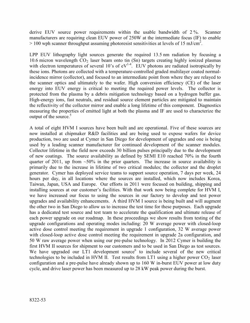
2. LPP SOURCE SYSTEM
The system architecture is shown in a scale drawing in Figure 1. The three major subsystems of the source are the drive laser, the beam transport system (BTS) and the source vessel. The drive laser is a CO2 laser with multiple stages of amplification to reach the required power level of up to ~30 kW.7,8 It is operated in pulsed mode at ~50 kHz with radio-frequency (RF) pumping from generators (not shown) operating at 13.56 MHz. The laser is typically installed in the sub-fab along with its RF generators and water-to-water heat exchangers. The laser beam is expanded as it leaves the drive laser to lower the energy density on the BTS mirrors and allows higher NA for focusing the beam to small spot size. Three turning mirrors are used to allow the beam to travel from the sub-fab to the fab through the waffle-slab floor with the needed flexibility for positioning the laser with respect to the source vessel (and scanner) on the floor above. The laser and BTS are completely enclosed and interlocked to meet laser class 1 requirements. The BTS delivers the beam to a focusing optic where the light at 10.6 µm wavelength is focused to a minimum spot size defined by the numerical aperture of the focusing system. The converging beam propagates through a central aperture in the collector and strikes the droplet at the focus of the ellipsoidal collector mirror inside the vacuum space of the source vessel. The droplet generator delivers liquid tin droplets of 30 µm diameter to the same position at ~50 kHz repetition rate; both laser pulse and droplets are steered and timed to ensure proper targeting. The laser pulse vaporizes and heats the tin into a plasma cloud of critical temperature and density. The EUV light emitted by the plasma is collected and reflected with the multilayer-coated ellipsoidal mirror to the IF where it passes through a small aperture into the scanner volume that houses the illumination optics.
Figure 1: Scale Drawing of Laser Produced Plasma Source.
Laser Metrology
Vacuum Vessel with Collector
Turning Mirror
Turning Mirror
Class 1 Drive Laser System
Turning Mirror
Sealed Beam Tubes
Sealed Beam Tubes
Isolation Frame
Laser Metrology
Vacuum Vessel with Collector
Turning Mirror
Turning Mirror
Class 1 Drive Laser System
Turning Mirror
Sealed Beam Tubes
Sealed Beam Tubes
Isolation Frame
8322-53
To ensure that no contamination can reach the scanner volume an IF protection module surrounds the aperture and suppresses flow and diffusion9. Other modules on the source vessel include the droplet catcher which collects the unused droplets between the bursts, and metrology modules used to measure EUV energy and to image droplets and plasma. The source controller turns on and off bursts of pulses as commanded by the scanner, which can be as long as several seconds. Exposures at full source power correspond to typically several hundred milliseconds for a 26 x 33mm field size using 15 – 20 mJ/cm2 resist. The ratio of time when the burst is on to the period between bursts defines the intra-field duty cycle.
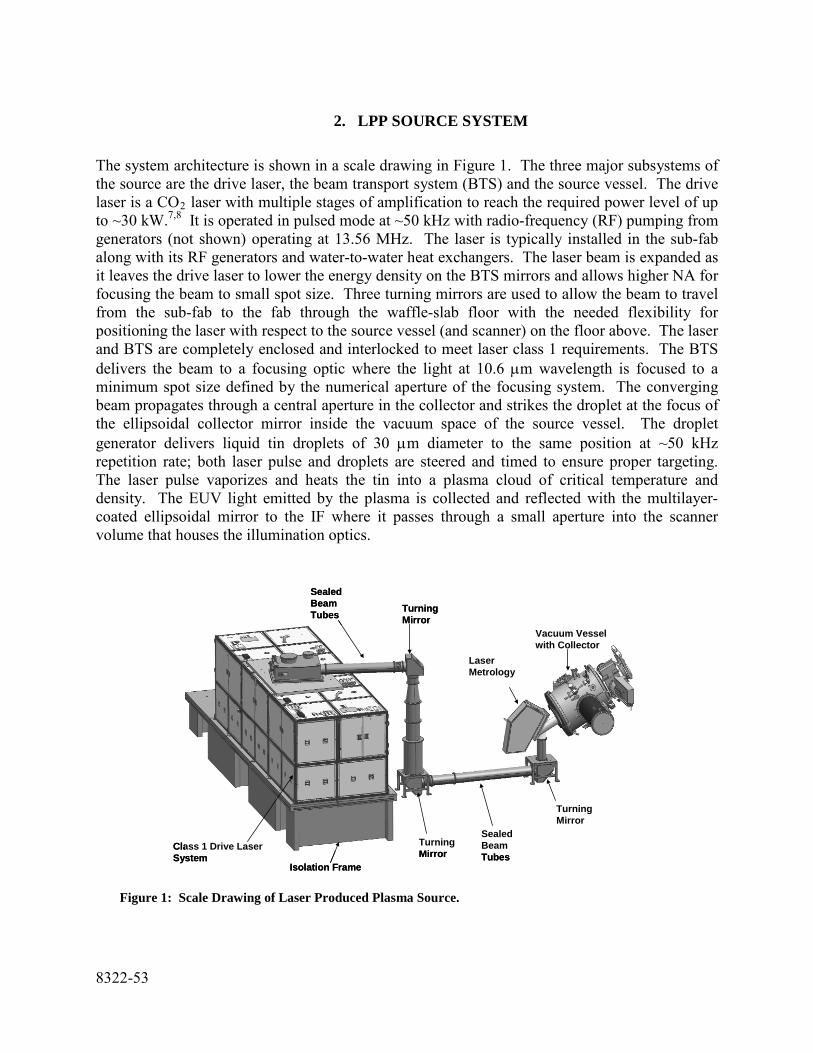
3. RECENT DEVELOPMENT RESULTS Results of testing in San Diego on our internal test source Pilot 8 were used to qualify our upgrade 1 performance at 20W average power. During this test the source was being driven by a scanner simulator which mimics the actual operation of the source during wafer exposures in a fab. This allows us to post-process the results and evaluate many parameters including dose stability by individual die as shown in Figure 2. Each die has better than the required ±0.5% 3σ dose stability as shown in the wafer maps. These are just two of over 1000 wafers simulations run as part of the qualification. The test concluded with more than 99.7% of the dies on all wafer simulations meeting dose stability requirements and allowed qualification of the upgrade and its release to the field.
Figure 2: 20W Average Power Dose Stability Die to Die
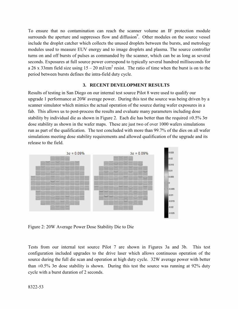
Tests from our internal test source Pilot 7 are shown in Figures 3a and 3b. This test configuration included upgrades to the drive laser which allows continuous operation of the source during the full die scan and operation at high duty cycle. 32W average power with better than ±0.5% 3σ dose stability is shown. During this test the source was running at 92% duty cycle with a burst duration of 2 seconds.
8322-53
Figure 3a: 32W Average Power with better than ±0.5% dose stability
Figure 3b: Dose Stability Histogram at 32W
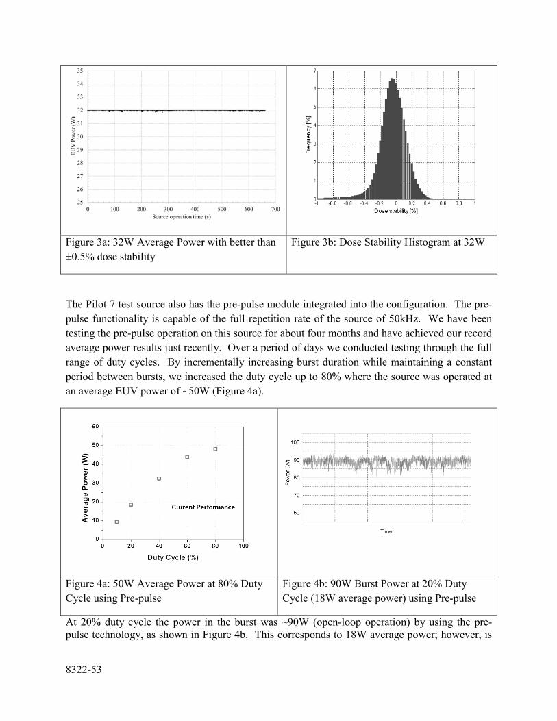
The Pilot 7 test source also has the pre-pulse module integrated into the configuration. The pre-pulse functionality is capable of the full repetition rate of the source of 50kHz. We have been testing the pre-pulse operation on this source for about four months and have achieved our record average power results just recently. Over a period of days we conducted testing through the full range of duty cycles. By incrementally increasing burst duration while maintaining a constant period between bursts, we increased the duty cycle up to 80% where the source was operated at an average EUV power of ~50W (Figure 4a).
Figure 4a: 50W Average Power at 80% Duty Cycle using Pre-pulse
Figure 4b: 90W Burst Power at 20% Duty Cycle (18W average power) using Pre-pulse
At 20% duty cycle the power in the burst was ~90W (open-loop operation) by using the pre-pulse technology, as shown in Figure 4b. This corresponds to 18W average power; however, is
8322-53
important to show the capability of the source to create levels very close to the final 100W power target, which is expected to be completed by the end of the year.
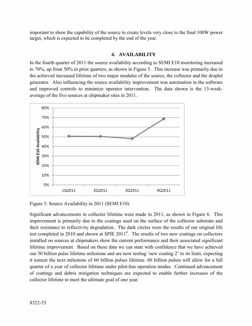
4. AVAILABILITY In the fourth quarter of 2011 the source availability according to SEMI E10 monitoring increased to 70%, up from 50% in prior quarters, as shown in Figure 5. This increase was primarily due to the achieved increased lifetime of two major modules of the source, the collector and the droplet generator. Also influencing the source availability improvement was automation in the software and improved controls to minimize operator intervention. The data shown is the 13-week-average of the five sources at chipmaker sites in 2011.
Figure 5: Source Availability in 2011 (SEMI E10)
Significant advancements in collector lifetime were made in 2011, as shown in Figure 6. This improvement is primarily due to the coatings used on the surface of the collector substrate and their resistance to reflectivity degradation. The dark circles were the results of our original life test completed in 2010 and shown at SPIE 20114. The results of two new coatings on collectors installed on sources at chipmakers show the current performance and their associated significant lifetime improvement. Based on these data we can state with confidence that we have achieved our 30 billion pulse lifetime milestone and are now testing ‘new coating 2’ to its limit, expecting it tomeet the next milestone of 60 billion pulses lifetime. 60 billion pulses will allow for a full quarter of a year of collector lifetime under pilot-line operation modes. Continued advancement of coatings and debris mitigation techniques are expected to enable further increases of the collector lifetime to meet the ultimate goal of one year.

8322-53
Figure 6: Recent Collector Lifetime Result for Sources in the Field
Extending the lifetime of the droplet generator is a major focus of our development at Cymer. Reliability improvements in 2011 were significant and have allowed us to now consider modes of operation that use the components for much longer period of time, rather than replacing them frequently. Still, today in the field the maximum usage time is about one week, as it is limited by the volume of tin stored in the generator reservoir. The generator reaches this lifetime only if no component failures occur. By eliminating the failure modes and increasing the size of the reservoir, or by refilling it in-situ, the run time of this critical module can be increased. Data from testing a droplet generator on a test stand at Cymer over a period of 46 days are shown in Figure 7. These results show the capability of the component to run for this extended period of time and not to deteriorate or lose stability. This new mode of operation is also being used on our internal sources where we have recently achieved 800 hours of droplet generator operation while producing EUV light.
Figure 7a: Day 1 Droplet Stability Figure 7b: Day 46 Droplet Stability
As shown at SPIE 2011
New coating 1 New coating 2
8322-53
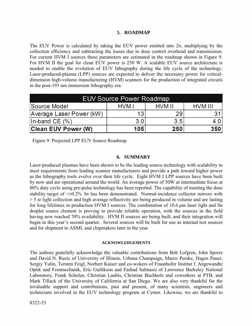
5. ROADMAP The EUV Power is calculated by taking the EUV power emitted into 2π, multiplying by the collection efficiency and subtracting the losses due to dose control overhead and transmission. For current HVM I sources these parameters are estimated in the roadmap shown in Figure 9. For HVM II the goal for clean EUV power is 250 W. A scalable EUV source architecture is needed to enable the evolution of EUV lithography during the life cycle of the technology. Laser-produced-plasma (LPP) sources are expected to deliver the necessary power for critical-dimension high-volume manufacturing (HVM) scanners for the production of integrated circuits in the post-193 nm immersion lithography era.
Figure 9: Projected LPP EUV Source Roadmap
6. SUMMARY Laser-produced plasmas have been shown to be the leading source technology with scalability to meet requirements from leading scanner manufacturers and provide a path toward higher power as the lithography tools evolve over their life cycle. Eight HVM I LPP sources have been built by now and are operational around the world. An average power of 50W at intermediate focus at 80% duty cycle using pre-pulse technology has been reported. The capability of meeting the dose stability target of <±0.2% 3σ has been demonstrated. Normal-incidence collector mirrors with > 5 sr light collection and high average reflectivity are being produced in volume and are lasting for long lifetimes in production HVM I sources. The combination of 10.6 μm laser light and Sn droplet source element is proving to provide reliable operation, with the sources in the field having now reached 70% availability. HVM II sources are being built, and their integration will begin in this year’s second quarter. Several sources will be built for use as internal test sources and for shipment to ASML and chipmakers later in the year.
ACKNOWLEDGEMENTS The authors gratefully acknowledge the valuable contributions from Bob Lofgren, John Sporre and David N. Ruzic of University of Illinois, Urbana Champaign, Marco Perske, Hagen Pauer, Sergiy Yulin, Torsten Feigl, Norbert Kaiser and co-wokers of Fraunhofer Institut f. Angewandte Optik und Feinmechanik, Eric Gullikson and Farhad Salmassi of Lawrence Berkeley National Laboratory, Frank Scholze, Christian Laubis, Christian Buchholz and coworkers at PTB, and Mark Tillack of the University of California at San Diego. We are also very thankful for the invaluable support and contributions, past and present, of many scientists, engineers and technicians involved in the EUV technology program at Cymer. Likewise, we are thankful to
8322-53
many colleagues at ASML for helpful discussions of various aspects related to the light source operation.
REFERENCES
[1] Brandt, D.C., Fomenkov, I.V., Ershov, A.I., Partlo, W.N., Myers, D.W., Böwering, N.R., Farrar, N.R., Vaschenko, G.O., Khodykin, O.V., Bykanov, A.N., Hoffman, J.R., Chrobak, C.P, Srivastava, S.N., Ahmad, I., Rajyaguru, C., Golich, D.J., Vidusek, D.A., De Dea, S., Hou, R.R., in: Proc. of SPIE Vol. 7271, Alternative Lithographic Technologies, F. M. Schellenberg, B. M. La Fontaine, Eds., 727103, (2009). [2] Fomenkov, I.V., Brandt, D.C., Bykanov, A.N., Ershov, A.I., Partlo, W.N., Myers, D.W., Böwering, N.R., Farrar, N.R., Vaschenko, G.O., Khodykin, O.V., Hoffman, J.R., Chrobak, C.P., Srivastava, S.N., Golich, D.J., Vidusek, D.A., De Dea, S., Hou, R.R., in: Proc. of SPIE Vol. 7271, Alternative Lithographic Technologies, F. M. Schellenberg, B. M. La Fontaine, Eds., 727138 (2009). [3] Böwering, N.R., Fomenkov, I.V., Brandt, D.C., Bykanov, A.N., Ershov, A.I., Partlo, W.N., Myers, D.W., Farrar, N.R., Vaschenko, G.O., Khodykin, O.V., Hoffman, J.R., Chrobak, C.P., Srivastava, S.N., Ahmad, I., Rajyaguru, C., Golich, D.J., Vidusek, D.A., De Dea, S., Hou R.R.,, Journal of Micro/Nanolith. MEMS MOEMS 8(4), 041504 (2009). [4] Brandt, D.C, Fomenkov, I.V., Ershov, A.I., Partlo, W.N., Myers, D.W., Sandstrom, R.L., La Fontaine, B.M., Lercel, M.J., Bykanov, A.N., Böwering, N.R., Vaschenko, G.O., Khodykin, O.V., Srivastava, S.N., Ahmad, I., Rajyaguru, C., Das, P., Fleurov, V.B., Zhang, K., Golich, D.J., De Dea, S., Hou, R.R., Dunstan, W.J., Wittak, C.J., Baumgart, P., Ishihara, T., Simmons, R.D., Jacques, R.N., Bergstedt, R.A., in: Proc. of SPIE Vol. 7969, Extreme Ultraviolet (EUV) Lithography II, B. M. La Fontaine, P. P. Naulleau, Eds., 79691H (2011). [5] Böwering, N.R., Hoffman, J.R., Khodykin, O.V., Rettig, C.L., Hansson, B.A.M., Ershov, A.I., Fomenkov, I.V., in: Proc. SPIE Vol. 5752, Metrology, Inspection, and Process Control for Microlithograpy XIX, R. M. Silver, Ed., 1248-1256 (2005). [6] Brandt, D.C., Fomenkov, I.V., Ershov, A.I., Partlo, W.N., Myers, D.W., Böwering, N.R., Bykanov, A.N., Vaschenko, G.O., Khodykin, O.V., Hoffmann, J. R., Vargas E.L., Simmons, R.D., Chavez, J.A., Chrobak, C.P., in: Proc. of SPIE Vol. 6517, Emerging Lithographic Technologies XI, M. J. Lercel, ED., 65170Q (2007). [7] Fomenkov, I.V., Hansson, B.A.M., Böwering, N.R., Ershov, A.I., Partlo, W.N., Fleurov, V.B., Khodykin, O.V., Bykanov, A.N., Rettig, C.L., Hoffman, J.R., Vargas E.L., Chavez, J.A., Marx, W.F., Brandt, D.C., in: Proc. of SPIE Vol. 6151, Emerging Lithographic Technologies X, M. J. Lercel, Ed., 61513X (2006). [8] Fomenkov, I.V., Brandt, D.C., Bykanov, A.N., Ershov, A.I., Partlo, W.N., Myers, D.W., Böwering, N.R., Vaschenko, G.O., Khodykin, O.V., Hoffman, J.R., Vargas, E., L., Simmons, R.D., Chavez, J.A., Chrobak, C.P., in: Proc. of SPIE Vol. 6517, Emerging Lithographic Technologies XI, M. J. Lercel, ED., 65173J (2007). [9] Fomenkov, I.V., Ershov, A.I., Partlo, W.N., Myers, D.W., Brown, D., Sandstrom, R.L., La Fontaine, B.M., Bykanov, A.N., Vaschenko, G.O., Khodykin, O.V., Böwering, N.R., Das, P., Fleurov, V.B., Zhang, Srivastava, S.N., Ahmad, I., Rajyaguru, C., De Dea, S., Hou, R.R., Dunstan, W.J., Baumgart, P., Ishihara, T., Simmons, R.D., Jacques, R.N., Bergstedt, R.A., Brandt, D.C., in: Proc. of SPIE Vol. 7969, Extreme Ultraviolet (EUV) Lithography II, B. M. La Fontaine, P. P. Naulleau, Eds., 796933 (2011).

Enhancing Lithography Process Control Through Advanced, On-board Beam Parameter Metrology for Wafer Level Monitoring of
Light Source Parameters
Jinphil Choia, Nakgeuon Seongb, Omar Zuritab, Joshua Thornesb, Yookeun Wonb, Slava Rokitskib, Youngseog Kanga, Bernd Burfeindtb, Chanhoon Parka
aSamsung Electronics Co, San #16 Banwol-Dong, Hwasung-City, Gyeonggi-Do; bCymer Inc., 17075 Thornmint Court, San Diego, CA, 92127, USA
ABSTRACT
In order to improve process control of the lithography process, enhanced On-board metrology, measuring of the light source beam parameters with software solutions for monitoring, reporting and analyzing the light source’s performance has been introduced.
Multiple lasers in the field were monitored after installing of a new On-board metrology product called SmartPulse. It was found that changes in beam parameters can be significantly reduced at major module change service events when new service procedures and On-board metrology were used, while significant beam parameter shift and illumination pupil changes were observed when On-board metrology was not available at service events, causing lengthy scanner illumination pupil recalibration.
SmartPulse™ software from Cymer Inc. was used to monitor the variation of light source performance parameters, including critical beam parameters, at wafer level resolution. Wafer CD was correlated to the recorded beam parameters for about a month of operation, and both wafer CD and beam parameters showed stable performance when the light source was operating at optimal conditions.
Keywords: Photo-lithography, On-board metrology, Laser beam parameter, Light source performance parameter monitoring
1. INTRODUCTION The monitoring and control of process parameters at the process tool level has been used to improve process stability without increasing direct off-line wafer metrology, enabling fast wafer turn-around time and fab capital cost reduction[1] . The need to provide process monitoring capability with higher resolution and additional process parameters at the light source level has been observed.
1.1 Process monitoring and control improvement
As the use of ArF immersion lithography processes for most critical layer patterning has continued for multiple technology generations, each lithographic imaging solution has become highly optimized for specific patterns to be printed. Use of different imaging solutions for different device patterns also drives different levels of control for process variables. For example, highly optimized SMO(source mask optimization) imaging solutions require tighter control of the illumination pupil than simple SDP (Spacer double pattering) with dipole illumination. Very high throughput lithography patterning processes were implemented to reduce the cost of multiple patterning processes, which are commonly used for memory device production. It has been recognized that smaller pattern size and lower k1 imaging processes at the latest technology nodes drive tighter control of more process performance parameters of lithography tools than at previous nodes. Process parameter monitoring and control for the process tools has been adopted as a way of reducing process errors and improving process control, and minimizing added metrology capital costs.(Figure 1.)
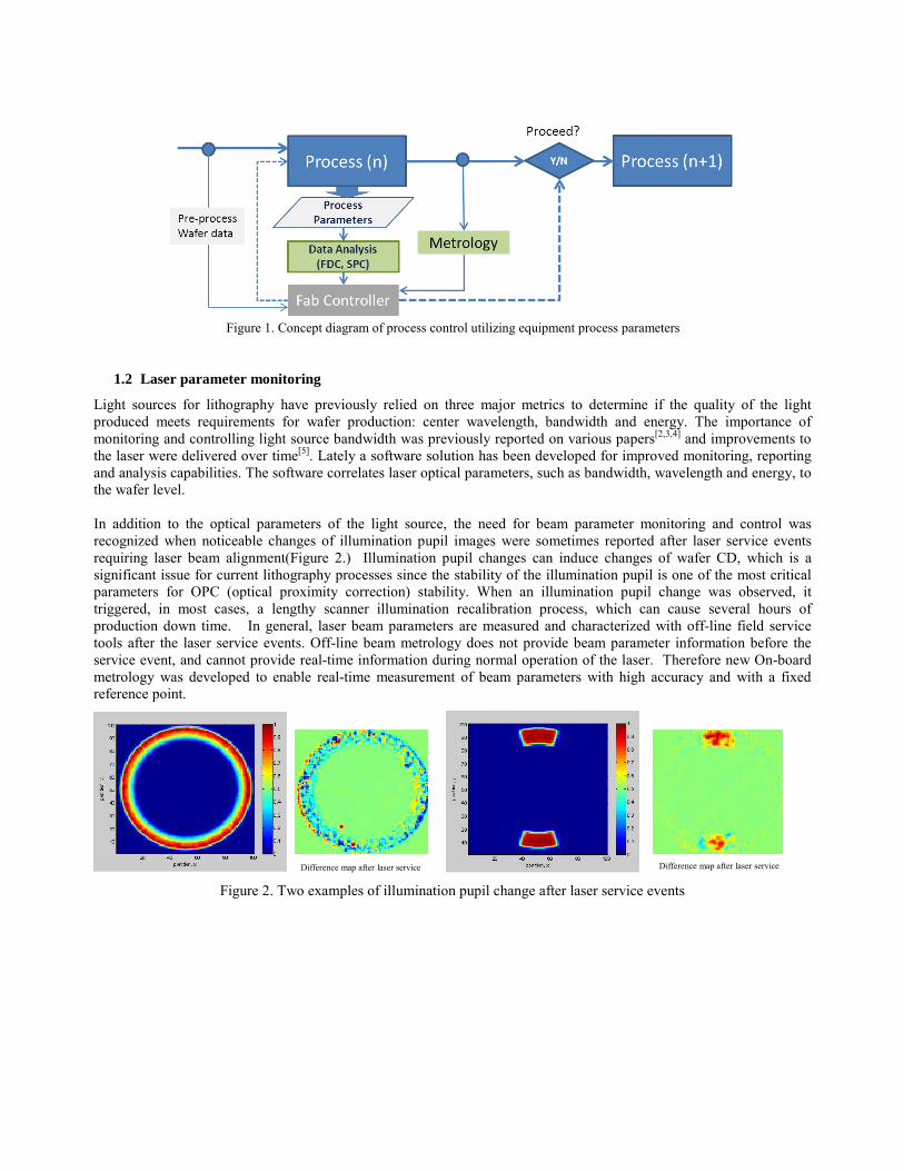
Figure 1. Concept diagram of process control utilizing equipment process parameters
1.2 Laser parameter monitoring
Light sources for lithography have previously relied on three major metrics to determine if the quality of the light produced meets requirements for wafer production: center wavelength, bandwidth and energy. The importance of monitoring and controlling light source bandwidth was previously reported on various papers[2,3,4] and improvements to the laser were delivered over time[5]. Lately a software solution has been developed for improved monitoring, reporting and analysis capabilities. The software correlates laser optical parameters, such as bandwidth, wavelength and energy, to the wafer level. In addition to the optical parameters of the light source, the need for beam parameter monitoring and control was recognized when noticeable changes of illumination pupil images were sometimes reported after laser service events requiring laser beam alignment(Figure 2.) Illumination pupil changes can induce changes of wafer CD, which is a significant issue for current lithography processes since the stability of the illumination pupil is one of the most critical parameters for OPC (optical proximity correction) stability. When an illumination pupil change was observed, it triggered, in most cases, a lengthy scanner illumination recalibration process, which can cause several hours of production down time. In general, laser beam parameters are measured and characterized with off-line field service tools after the laser service events. Off-line beam metrology does not provide beam parameter information before the service event, and cannot provide real-time information during normal operation of the laser. Therefore new On-board metrology was developed to enable real-time measurement of beam parameters with high accuracy and with a fixed reference point.
Figure 2. Two examples of illumination pupil change after laser service events
Difference map after laser service Difference map after laser service
2. ON-BOARD LASER METROLOGY Advanced, On-board beam parameter metrology is offered as an upgrade to Cymer’s industry leading XL light source platform. This upgrade adds new capability to the platform by providing a new metrology system with significantly expanded in-situ metrology capabilities. This expands the existing metrology on the XL platform to make available to the chipmaker beam parameter measurements in addition to the already available data on energy, wavelength and bandwidth.
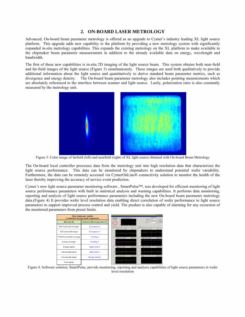
The first of these new capabilities is in-situ 2D imaging of the light source beam. This system obtains both near-field and far-field images of the light source (Figure 3) simultaneously. These images are used both qualitatively to provide additional information about the light source and quantitatively to derive standard beam parameter metrics, such as divergence and energy density. The On-board beam parameter metrology also includes pointing measurements which are absolutely referenced to the interface between scanner and light source. Lastly, polarization ratio is also constantly measured by the metrology unit.
Figure 3: Color image of farfield (left) and nearfield (right) of XL light source obtained with On-board Beam Metrology
The On-board local controller processes data from the metrology unit into high resolution data that characterizes the light source performance. This data can be monitored by chipmakers to understand potential wafer variability. Furthermore, the data can be remotely accessed via CymerOnLine® connectivity solution to monitor the health of the laser thereby improving the accuracy of service event prediction.
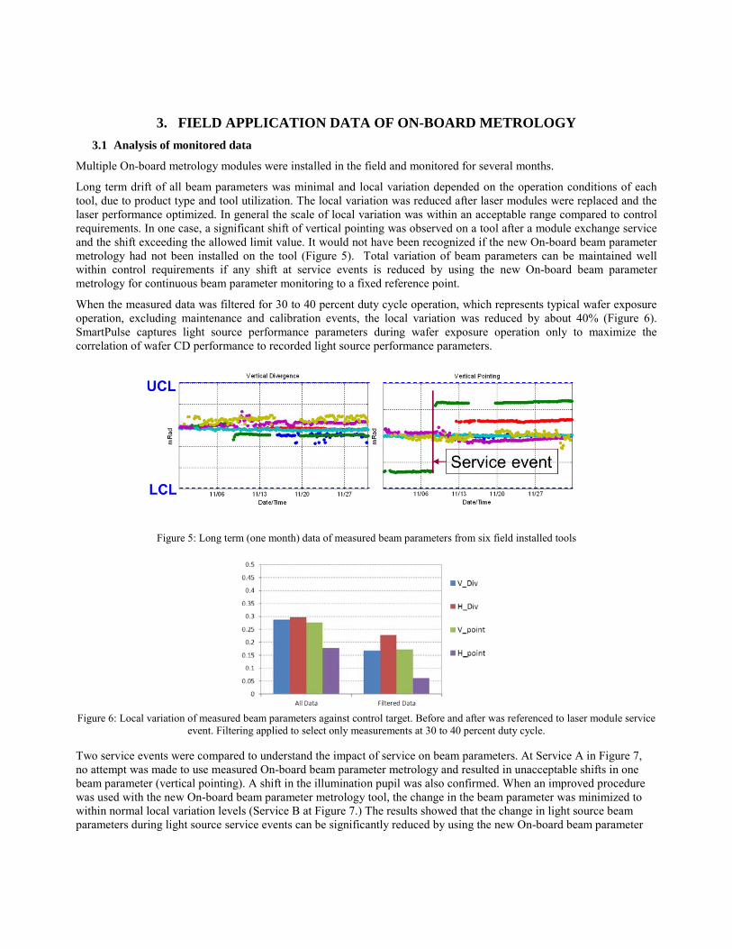
Cymer’s new light source parameter monitoring software , SmartPulse™, was developed for efficient monitoring of light source performance parameters with built in statistical analysis and warning capabilities. It performs data monitoring, reporting and analysis of light source performance parameters including the new On-board beam parameter metrology data.(Figure 4) It provides wafer level resolution data enabling direct correlation of wafer performance to light source parameters to support improved process control and yield. The product is also capable of alarming for any excursion of the monitored parameters from preset limits.
Figure 4: Software solution, SmartPulse, provide monitoring, reporting and analysis capabilities of light source parameters in wafer level resolution
3. FIELD APPLICATION DATA OF ON-BOARD METROLOGY 3.1 Analysis of monitored data
Multiple On-board metrology modules were installed in the field and monitored for several months.
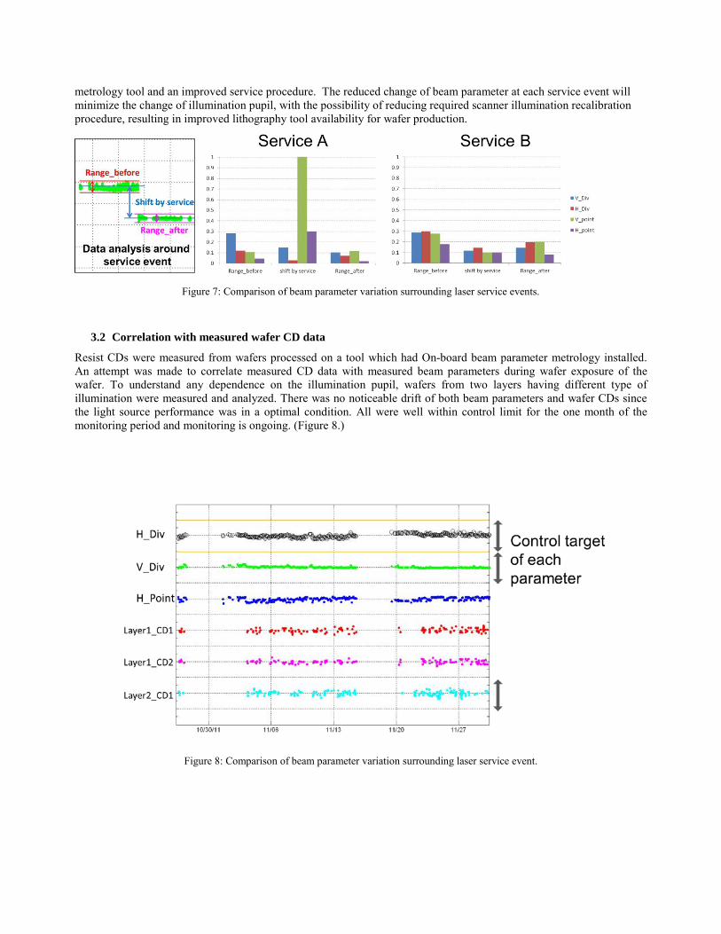
Long term drift of all beam parameters was minimal and local variation depended on the operation conditions of each tool, due to product type and tool utilization. The local variation was reduced after laser modules were replaced and the laser performance optimized. In general the scale of local variation was within an acceptable range compared to control requirements. In one case, a significant shift of vertical pointing was observed on a tool after a module exchange service and the shift exceeding the allowed limit value. It would not have been recognized if the new On-board beam parameter metrology had not been installed on the tool (Figure 5). Total variation of beam parameters can be maintained well within control requirements if any shift at service events is reduced by using the new On-board beam parameter metrology for continuous beam parameter monitoring to a fixed reference point.
When the measured data was filtered for 30 to 40 percent duty cycle operation, which represents typical wafer exposure operation, excluding maintenance and calibration events, the local variation was reduced by about 40% (Figure 6). SmartPulse captures light source performance parameters during wafer exposure operation only to maximize the correlation of wafer CD performance to recorded light source performance parameters.
Figure 5: Long term (one month) data of measured beam parameters from six field installed tools
Figure 6: Local variation of measured beam parameters against control target. Before and after was referenced to laser module service event. Filtering applied to select only measurements at 30 to 40 percent duty cycle.
Two service events were compared to understand the impact of service on beam parameters. At Service A in Figure 7, no attempt was made to use measured On-board beam parameter metrology and resulted in unacceptable shifts in one beam parameter (vertical pointing). A shift in the illumination pupil was also confirmed. When an improved procedure was used with the new On-board beam parameter metrology tool, the change in the beam parameter was minimized to within normal local variation levels (Service B at Figure 7.) The results showed that the change in light source beam parameters during light source service events can be significantly reduced by using the new On-board beam parameter
metrology tool and an improved service procedure. The reduced change of beam parameter at each service event will minimize the change of illumination pupil, with the possibility of reducing required scanner illumination recalibration procedure, resulting in improved lithography tool availability for wafer production.
Figure 7: Comparison of beam parameter variation surrounding laser service events.
3.2 Correlation with measured wafer CD data
Resist CDs were measured from wafers processed on a tool which had On-board beam parameter metrology installed. An attempt was made to correlate measured CD data with measured beam parameters during wafer exposure of the wafer. To understand any dependence on the illumination pupil, wafers from two layers having different type of illumination were measured and analyzed. There was no noticeable drift of both beam parameters and wafer CDs since the light source performance was in a optimal condition. All were well within control limit for the one month of the monitoring period and monitoring is ongoing. (Figure 8.)
Figure 8: Comparison of beam parameter variation surrounding laser service event.

4. SUMMARY A new On-board metrology module, which measures beam parameters of the light source in real-time, and SmartPulse light source parameter monitoring software, were introduced by Cymer to improve process stability, especially proximity effect for OPC stability.
Real-time monitoring of light source performance parameters during wafer exposures will enable a correlation with CD performance on the wafers as well as laser health status.
The new On-board beam parameter metrology can be used to minimize the change of beam parameters to avoid lengthy illuminator pupil calibration after light source service by using an improved service procedure.
Stable CD performance was observed with stable beam parameter performance of optimal laser operation.
REFERENCES
[1] ITRS 2010, ‘Factory Integration Chapter’ [2] Brunner et al, “Laser bandwidth and other sources of focus blur in lithography,” Proc. 6154 (2006). [3] K. Huggins et al., “Effects of laser bandwidth on OPE in a modern lithography tool,” Proc. SPIE 6154 (2006). [4] N. Seong et al., “Analyses of the effect of laser bandwidth on imaging of memory patterns,” Proc. SPIE 7140 (2008) [5] S. Rokitski et al., “Flexible 60-90W ArF light source for double patterning immersion lithography in high volume
manufacturing”, Proc. SPIE 7520 (2009)
Process requirements for pitch splitting LELE double patterning at advanced logic technology node
R. C. Peng*a, I. H. Huanga, H. H. Liua, H. J. Leea, John Lina, Arthur Linb, Allen Changc, Benjamin
Szu-Min Linc and Ivan Lalovicd
aMTC, Taiwan Semiconductor Manufacturing Corp., Hsinchu Science Park, Hsinchu, Taiwan 300-77, R.O.C.; bKLA-Tencor Corp., Chupei City, Hsinchu, Taiwan, R.O.C.; cCymer Southeast Asis Ltd.,
Kuang Fu Rd. HsinChu, Taiwan, R.O.C., dCymer Inc., San Diego, CA, USA
ABSTRACT
As IC dimensions continue to shrink beyond the 22nm node, optical single exposure cannot sustain the resolution required and various double patterning techniques have become the main stream prior to the availability of EUV lithography. Among various kinds of double patterning techniques, positive splitting pitch lithography-etch-lithography-etch (LELE) double patterning is chosen for printing complex foundry circuit designs. Tighter circuit CD and process margin control in such positive splitting pitch LELE double patterning process becomes increasingly critical especially for topography issues induced by the 1st mask patterning with the 2nd mask exposure. In this paper, laser parameters, topography issues with the 2nd mask exposure, and SMO effects on CD performances are described in terms of the proximity CD portion of the scanner CD budget. Laser parameters, e.g. spectral shape and bandwidth, were input into the photolithography simulator, Prolith, to calculate their impacts on circuit CD variation. Mask-bias dependent lithographic performance was calculated and used to illustrate the importance of well-controlled laser performance parameters. Recommended laser bandwidth, mask bias and topography requirements are proposed, based on simulation results to ensure that the tight CD control (< 1nm) required for advanced technology node products can be achieved.
Keywords: CD control, topography, laser spectrum, photolithography simulation
1. INTRODUCTION As critical dimension (CD) shrunk following Moore’s Law, tight circuit CD control becomes more and more difficult, because of not only the reduced CD tolerance, but also hitting the equipment control limitations and CD measurement limitations. There are many factors that impact CD variations, for example, CD uniformity on reticles, focus errors, lens aberrations, partial coherence variation, photoresist performance and laser spectrum. Laser bandwidth and illumination partial coherence are two of the largest contributors to the proximity CD portion of the scanner CD budget, in the other words, Iso-Dense Bias (IDB) or through-pitch performance. IDB performance can be attributed to numerous factors that generate changes in image contrast or induce focus blur, for examples, illumination condition adjustment and laser light source spectral bandwidth (E95%). These factors are necessary to be controlled to fully compensate for IDB variation to the level required at advanced process nodes.[1]-[7]
Double patterning (DP) technology is widely used for 30nm Half Pitch and below, because EUV technology is not ready for high volume manufacturing at this moment due to low EUV source power, poor PR LWR performances, and lack of EUV mask infrastructure. Figure 1 shows different kinds of DP technologies published in the literature[8]-[11]. Some of them, e.g. self-alignment type DP, are suitable for memory products due to simple CD targets and regular dense pitch patterns in memory cell area. For random logic design patterns, positive splitting pitch Litho-Etching-Litho-Etching (LELE) type DP is the most suitable and ready-to-go technology, except for the tight and complicated overlay challenges between either same DP layers or different lithographic layers. In this manuscript, the effects of laser bandwidth and illumination setting on CD control for positive splitting pitch type LELE DP process will be discussed.
The other impacting factor to CD performances in positive splitting pitch type LELE DP processes compared to normal single patterning processes is topography generated by the first Litho-etching process in LELE DP process sequences. This topography step height can only be compensated by deposition of preceding layer materials and photoresist and
BAC layer coating during the 2nd lithographic processes. This topography effect on the 2nd lithographic process performances will be also discussed in this work.
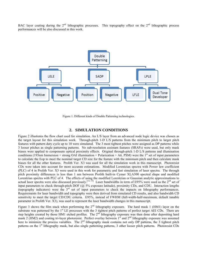
Figure 1. Different kinds of Double Patterning technologies.
2. SIMULATION CONDITIONS Figure 2 illustrates the flow chart used for simulation. An L/S layer from an advanced node logic device was chosen as the target layout for this simulation work. Through-pitch 1-D L/S patterns from the minimum pitch to larger pitch features with pattern duty cycle up to 10 were simulated. The 3 most tightest pitches were assigned as DP patterns while 3 looser pitches as single patterning patterns. No sub-resolution assistant features (SRAFs) were used, but only mask biases were applied to compensate optical proximity effects. Original through-pitch 1-D L/S patterns and illumination conditions (193nm Immersion + strong OAI illumination + Polarization + Att. PSM) were the 1st set of input parameters to calculate the Eop to meet the nominal target CD size for the feature with the minimum pitch and then calculate mask biases for all the other features. Prolith Ver. X3 was used for all the simulation work in this manuscript. Photoresist CDs were taken into account for more accurate estimations. Modified Lorentzian spectra with Power law coefficient (PLC) of 4 in Prolith Ver. X3 were used in this work for parametric and fast simulation of laser spectra. The through pitch proximity differences is less than 1 nm between Prolith built-in Cymer XLA300 spectral shape and modified Lorentzian spectra with PLC of 4. The effects of using the modified Lorentzian or Gaussian analytic approximations to actual laser spectra were also discussed previously.[12, 13] Laser bandwidths in term of E95% were used as the 2nd set of input parameters to check through-pitch DOF (@ 5% exposure latitude), proximity CDs, and CDU. Interaction lengths (topography indicators) were the 3rd set of input parameters to check the impacts on lithography performances. Requirements for laser bandwidth and topography were then derived from simulated CD results, and also bandwidth CD sensitivity to meet the target CD/CDU criteria. E95%, instead of FWHM (full-width-half-maximum, default tunable parameter in Prolith Ver. X3), was used to represent the laser bandwidth changes in this manuscript.
Figure 3 shows the film stack when performing the 2nd lithography exposure. The hard mask 1 (HM1) layer on the substrate was patterned by the 1st LE processes with the 3 tightest pitch patterns of perfect target AEI CDs. There are step heights created by those HM1 etched profiles. The 2nd lithography exposure was then done after depositing hard mask 2 (HM2) and coating tri-layer photoresist. Perfect overlay between 1st and 2nd lithography exposure was assumed here to minimize the process variables. The 2nd lithography mask contains not only DP patterns, the 3 tightest pitch patterns on the 1st lithography mask, but also single patterning patterns, 3 other looser pitch patterns. Photoresist CDs
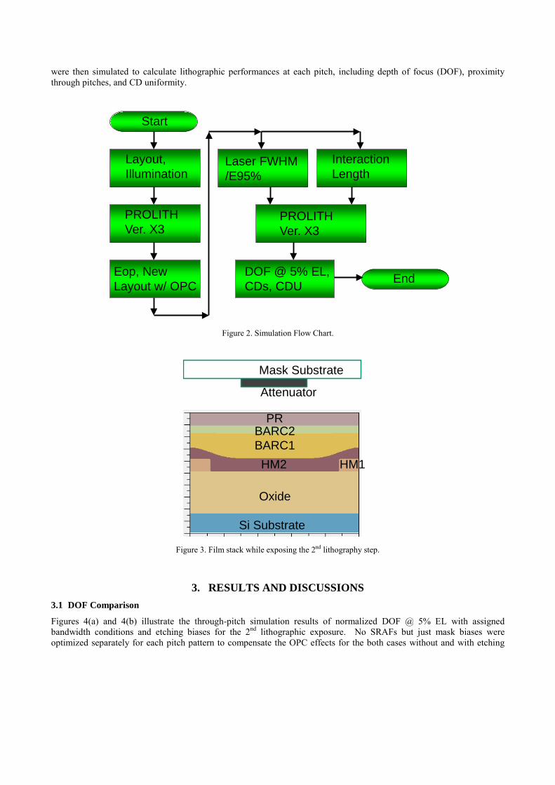
were then simulated to calculate lithographic performances at each pitch, including depth of focus (DOF), proximity through pitches, and CD uniformity.
Layout, Illumination
PROLITHVer. X3
Eop, New Layout w/ OPC
Laser FWHM/E95%
DOF @ 5% EL, CDs, CDU
InteractionLength
Start
End
PROLITHVer. X3
Figure 2. Simulation Flow Chart.
Si Substrate
Oxide
HM1HM2BARC1BARC2
PR
Mask Substrate
Attenuator
Figure 3. Film stack while exposing the 2nd lithography step.
3. RESULTS AND DISCUSSIONS 3.1 DOF Comparison
Figures 4(a) and 4(b) illustrate the through-pitch simulation results of normalized DOF @ 5% EL with assigned bandwidth conditions and etching biases for the 2nd lithographic exposure. No SRAFs but just mask biases were optimized separately for each pitch pattern to compensate the OPC effects for the both cases without and with etching
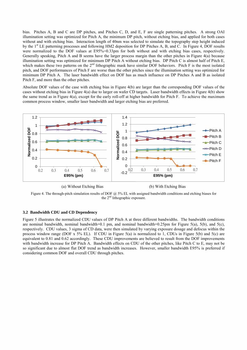
bias. Pitches A, B and C are DP pitches, and Pitches C, D, and E, F are single patterning pitches. A strong OAI illumination setting was optimized for Pitch A, the minimum DP pitch, without etching bias, and applied for both cases without and with etching bias. Interaction length of 40nm was selected to simulate the topography step height induced by the 1st LE patterning processes and following HM2 deposition for DP Pitches A, B, and C. In Figure 4, DOF results were normalized to the DOF values at E95%=0.33pm for both without and with etching bias cases, respectively. Generally speaking, Pitch A and B seems have the larger process margin than the other pitches in Figure 4(a) because illumination setting was optimized for minimum DP Pitch A without etching bias. DP Pitch C is almost half of Pitch E, which makes these two patterns on the 2nd lithographic mask have similar DOF behaviors. Pitch F is the most isolated pitch, and DOF performances of Pitch F are worse than the other pitches since the illumination setting was optimized for minimum DP Pitch A. The laser bandwidth effect on DOF has as much influence on DP Pitches A and B as isolated Pitch F, and more than the other pitches.
Absolute DOF values of the case with etching bias in Figure 4(b) are larger than the corresponding DOF values of the cases without etching bias in Figure 4(a) due to larger on wafer CD targets. Laser bandwidth effects in Figure 4(b) show the same trend as in Figure 4(a), except for the early roll-off at higher bandwidth for Pitch F. To achieve the maximum common process window, smaller laser bandwidth and larger etching bias are preferred.
0
0.2
0.4
0.6
0.8
1
1.2
0.2 0.3 0.4 0.5 0.6 0.7
Nor
mal
ized
DO
F
E95% (pm)
Pitch APitch BPitch CPitch DPitch EPitch F
-0.2
0
0.2
0.4
0.6
0.8
1
1.2
1.4
0.2 0.3 0.4 0.5 0.6 0.7
Nor
mal
ized
DO
F
E95% (pm)
Pitch APitch BPitch CPitch DPitch EPitch F
(a) Without Etching Bias (b) With Etching Bias
Figure 4. The through-pitch simulation results of DOF @ 5% EL with assigned bandwidth conditions and etching biases for the 2nd lithographic exposure.
3.2 Bandwidth CDU and CD Dependency
Figure 5 illustrates the normalized CDU values of DP Pitch A at three different bandwidths. The bandwidth conditions are nominal bandwidth, nominal bandwidth+0.1 pm, and nominal bandwidth+0.25pm for Figure 5(a), 5(b), and 5(c), respectively. CDU values, 3 sigma of CD data, were then simulated by varying exposure dosage and defocus within the process window range (DOF x 5% EL). If CDU in Figure 5(a) is normalized to 1, CDUs in Figure 5(b) and 5(c) are equivalent to 0.81 and 0.62 accordingly. These CDU improvements are believed to result from the DOF improvements with bandwidth increase for DP Pitch A. Bandwidth effects on CDU of the other pitches, like Pitch C to E, may not be so significant due to almost flat DOF trend as bandwidth increases. However, smaller bandwidth E95% is preferred if considering common DOF and overall CDU through pitches.

(a) (b) (c)
Figure 5. The normalized CDU values of DP Pitch A at three different bandwidths. The bandwidth conditions are nominal bandwidth, nominal bandwidth+0.1 pm, and nominal bandwidth+0.25pm for Figure 5(a), 5(b), and 5(c), respectively.
The bandwidth CD sensitivities of Pitches A and B with different etching biases in an E95% range of less than 0.5 pm were calculated in Figure 6. The relations between CD differences and laser bandwidth are very linear within this simulated laser bandwidth range for both without and with etching bias cases. The bandwidth CD sensitivities of Pitches A and B in the case of without etching bias are 2.3nm/0.1pm and 3.18nm/0.1pm. The CD variation is then derived as 0.53nm ~ 0.73nm, based on typical Cymer XLR long term performance at E95% 3 sigma of 23fm with active bandwidth control. The bandwidth CD sensitivities of Pitches A and B in the case of with etching bias are smaller at 0.94nm/0.1pm and 1.64nm/0.1pm. In this without etching bias case, CD variation can be improved down to 0.21nm ~ 0.37nm using the same typical Cymer XLR long term bandwidth performance. By further optimizing etching bias, the current Cymer XLR bandwidth performances can definitely meet the CD variation requirements for DP processes for the advanced logic nodes.
y = -23.014x + 13.189
y = -31.8x + 17.151-5
-2.5
0
2.5
5
0.25 0.35 0.45 0.55 0.65 0.75
CD
Diff
eren
ce (n
m)
E95% (pm)
Pitch A
Pitch .
Linear (Pitch A)
Linear (Pitch .)
y = -9.4581x + 5.5189
y = -16.406x + 8.2996
-5
-2.5
0
2.5
5
0.25 0.35 0.45 0.55 0.65 0.75
CD
Diff
eren
ce (n
m)
E95% (pm)
Pitch A
Pitch .
Linear (Pitch A)
Linear (Pitch .)
BW BW+0.1 BW+0.2 BW+0.3 BW+0.4 BW+0.5 BW BW+0.1 BW+0.2 BW+0.3 BW+0.4 BW+0.5
(a) Without Etching Bias (b) With Etching Bias
Figure 6. The bandwidth CD sensitivities of Pitches A and B in an E95% range of less than 0.5 pm.
Figure 7 shows the through-defocus photoresist profile comparison for DP Pitch A without etching bias, and with interaction length of 40 nm for the underneath stacks, at different bandwidth conditions. Bandwidth difference is 0.25 pm. Best energy and best defocus conditions were set at the center conditions for the through-defocus photoresist profile comparison at different bandwidths. For DP Pitch A, a little more T-top and footing were observed for larger bandwidth conditions than smaller bandwidth conditions, which could be an effect of chromatic defocus at the larger bandwidth. Although larger bandwidth conditions are preferred to have larger DOF for DP Pitch A, smaller bandwidth conditions should be better choices if considering photoresist profiles into account.
E95%
E95%+0.25pm
BF +DeFocus-DeFocus
Figure 7. The through-defocus photoresist profile comparison for DP Pitch A without etching bias and with interaction length of 40 nm for the underneath stacks at different bandwidth conditions.
3.3 Illumination Condition Effects
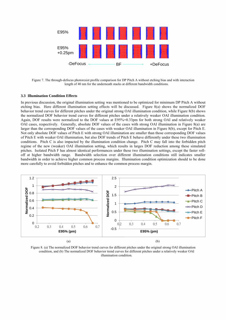
In previous discussion, the original illumination setting was mentioned to be optimized for minimum DP Pitch A without etching bias. Here different illumination setting effects will be discussed. Figure 8(a) shows the normalized DOF behavior trend curves for different pitches under the original strong OAI illumination condition, while Figure 8(b) shows the normalized DOF behavior trend curves for different pitches under a relatively weaker OAI illumination condition. Again, DOF results were normalized to the DOF values at E95%=0.33pm for both strong OAI and relatively weaker OAI cases, respectively. Generally, absolute DOF values of the cases with strong OAI illumination in Figure 8(a) are larger than the corresponding DOF values of the cases with weaker OAI illumination in Figure 8(b), except for Pitch E. Not only absolute DOF values of Pitch E with strong OAI illumination are smaller than those corresponding DOF values of Pitch E with weaker OAI illumination, but also DOF trends of Pitch E behave differently under these two illumination conditions. Pitch C is also impacted by the illumination condition change. Pitch C may fall into the forbidden pitch regime of the new (weaker) OAI illumination setting, which results in larges DOF reduction among these simulated pitches. Isolated Pitch F has almost identical performances under these two illumination settings, except the faster roll-off at higher bandwidth range. Bandwidth selection over different illumination conditions still indicates smaller bandwidth in order to achieve higher common process margins. Illumination condition optimization should to be done more carefully to avoid forbidden pitches and to enhance the common process margin.
0
0.2
0.4
0.6
0.8
1
1.2
0.2 0.3 0.4 0.5 0.6 0.7
Nor
mal
ized
DO
F
E95% (pm)
Pitch APitch BPitch CPitch DPitch EPitch F
-0.5
0
0.5
1
1.5
2
2.5
0.2 0.3 0.4 0.5 0.6 0.7
Nor
mal
ized
DO
F
E95% (pm)
Pitch APitch BPitch CPitch DPitch EPitch F
(a) (b)
Figure 8. (a) The normalized DOF behavior trend curves for different pitches under the original strong OAI illumination condition, and (b) The normalized DOF behavior trend curves for different pitches under a relatively weaker OAI
illumination condition.
3.4 Topography Effects
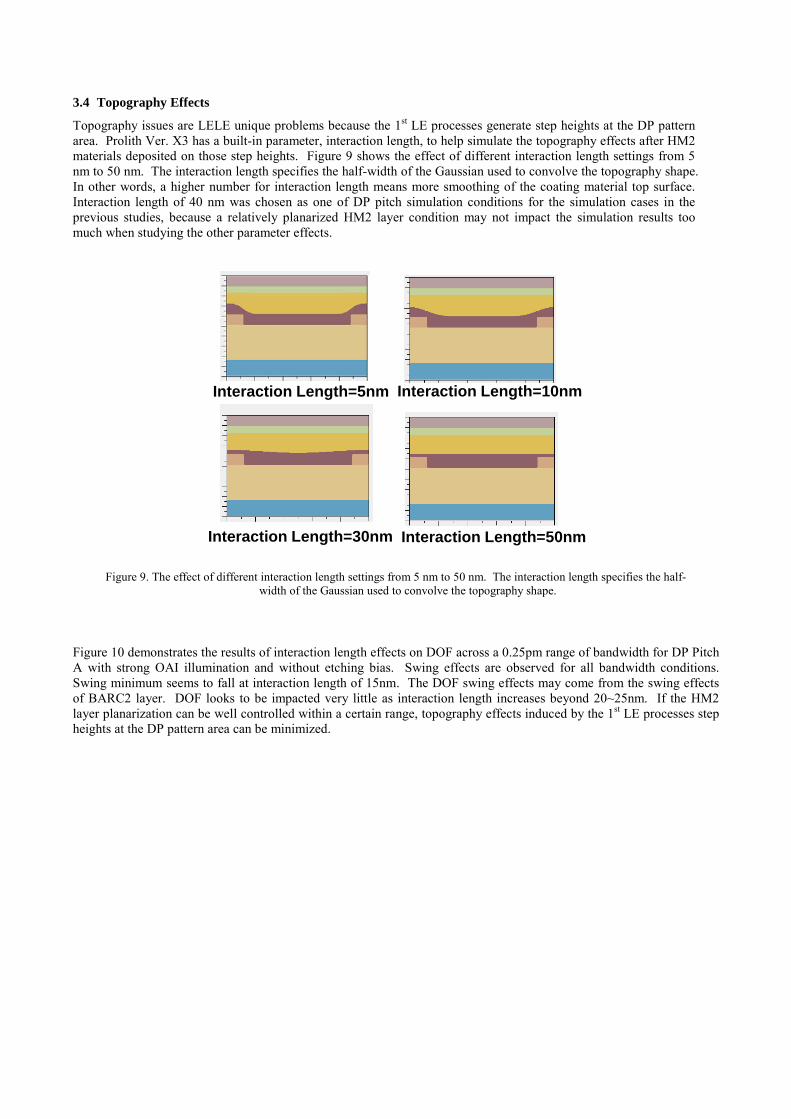
Topography issues are LELE unique problems because the 1st LE processes generate step heights at the DP pattern area. Prolith Ver. X3 has a built-in parameter, interaction length, to help simulate the topography effects after HM2 materials deposited on those step heights. Figure 9 shows the effect of different interaction length settings from 5 nm to 50 nm. The interaction length specifies the half-width of the Gaussian used to convolve the topography shape. In other words, a higher number for interaction length means more smoothing of the coating material top surface. Interaction length of 40 nm was chosen as one of DP pitch simulation conditions for the simulation cases in the previous studies, because a relatively planarized HM2 layer condition may not impact the simulation results too much when studying the other parameter effects.
Interaction Length=30nm Interaction Length=50nm
Interaction Length=10nmInteraction Length=5nm
Figure 9. The effect of different interaction length settings from 5 nm to 50 nm. The interaction length specifies the half-
width of the Gaussian used to convolve the topography shape.
Figure 10 demonstrates the results of interaction length effects on DOF across a 0.25pm range of bandwidth for DP Pitch A with strong OAI illumination and without etching bias. Swing effects are observed for all bandwidth conditions. Swing minimum seems to fall at interaction length of 15nm. The DOF swing effects may come from the swing effects of BARC2 layer. DOF looks to be impacted very little as interaction length increases beyond 20~25nm. If the HM2 layer planarization can be well controlled within a certain range, topography effects induced by the 1st LE processes step heights at the DP pattern area can be minimized.

5 10 15 20 25 30 35 40 45 50 55 60
Nor
mal
ized
DO
F (A
rb. U
nit)
Interaction Length (nm)
0.41250.4620.51150.5610.61050.66
BW
BW+0.05pm
BW+0.10pm
BW+0.15pm
BW+0.20pm
BW+0.25pm
Figure 10. The results of interaction length effects on DOF across a 0.25pm range of bandwidth for DP Pitch A.
4. CONCLUSION In this manuscript, bandwidth, etching bias, illumination and topography effects on positive splitting pitch type LELE DP process have been studied. Bandwidth, etching bias, and illumination have larger impacts on process margin than topography. To achieve the maximum common process window, larger etching bias is preferred. Etching bias and illumination settings may change DOF trends across bandwidth, however, smaller bandwidth at the current stabilized set-point is still preferred for obtaining larger common DOF, especially taking photoresist profiles into consideration. Bandwidth dependent CD variation of 0.21~0.37nm under suitable etching bias and optimal illumination conditions can be achieved with typical Cymer XLR long term bandwidth performance of 3 sigma of 23fm, which is enabled by advanced bandwidth stabilization and control technologies. It means that the current Cymer XLR bandwidth performances can definitely meet the CD variation requirements for DP processes for the advanced logic nodes. Topography effects have less impacts on DOF as interaction length increases beyond 20~25nm. Therefore, if the HM2 layer planarization can be well controlled within a certain range, topography effects induced by the 1st LE processes step heights for the DP pattern area can be minimized.
REFERENCE [1] M. Terry et al., “Behavior of lens aberrations as a function of wavelength on KrF and ArF lithography scanners”,
Optical Microlithography XIV, SPIE 4346-41 p.15-24 (2001). [2] T. Brunner et al., “Laser bandwidth and other sources of focus blur in lithography”, Optical Microlithography XIX,
SPIE 6154-31 (2006). [3] K. Huggins et al., “Effects of laser bandwidth on OPE in a modern lithography tool”, Optical Microlithography XIX,
SPIE 6154-36 (2006). [4] F. Trintchouk et al., “XLA 300: the Forth-Generation ArF MOPA Light Source for Immersion Lithography”, Optical
Microlithography XIX, SPIE 6154-76 (2006). [5] T. Oga et al., “Challenging to meet 1nm Iso- Dense Bias (IDB) by controlling Laser Spectrum”, Advanced
Lithography XXI, SPIE 6520-144 (2007). [6] K. Yoshimochi et al., “45nm Node Logic Device OPE Matching between Exposure Tools Through Laser Bandwidth
Tuning”, Optical Microlithography XXI, SPIE 6924-92 (2008). [7] K. Yoshimochi et al., “32nm Node Device Laser-bandwidth OPE Sensitivity and Process Matching”, Optical
Microlithography XXI, SPIE 7274-115 (2009).

[8] M. C. Chiu et al., “Challenges of 29nm half-pitch NAND Flash STI patterning with 193nm dry lithography and self-aligned double patterning”, Lithography Asia 2008, Proc. SPIE 714021 (2008)
[9] C. Fonseca et al., “Advances and challenges in dual-tone development process optimization”, Optical Microlithography XXII, Proc. SPIE 72740I (2009)
[10] C. Lim et al., “Positive and negative tone double patterning lithography for 50nm flash memory”, Optical Microlithography XIX, Proc. SPIE 615410 (2006)
[11] S. Tarutani et al., “Process parameter influence to negative tone development process for double patterning”, Advances in Resist Materials and Processing Technology XXVII, Proc. SPIE 76391Q (2010)
[12] I. Lalovic et al., “Defining a physically-accurate laser bandwidth input for optical proximity correction (OPC) and modeling”, Proc. BACUS XXII Photomask Technology Symposium 7122-62, (2008).
[13] R. C. Peng et al., “Laser spectrum requirements for tight CD control at advanced logic technology nodes”, Optical Microlithography XXIII, Proc. SPIE 76402C (2010)