Embed Size (px)
Citation preview

Advanced Coatings and Surface Engineering Laboratory Advanced Coatings and Surface Engineering Laboratory
Surface Engineering Task Repot2009/2/10

Advanced Coatings and Surface Engineering Laboratory Advanced Coatings and Surface Engineering Laboratory
Content
• Summary of the mechanical and tribological properties of CrN/AlN superlattice coatings
• High temperature oxidation study of CrN/AlN superlattice coatings
• Updates for the work of AlN ‘smart’ coatings
• Ready to use the Modulated pulse power (MPP) to produce the optimized coating system for the die casting dies

Advanced Coatings and Surface Engineering Laboratory Advanced Coatings and Surface Engineering Laboratory
Example of the Multilayered Superlattice Cr/CrxNy/CrN/AlN Coatings
75-500 single layers with bilayer period from 2.5 to 20 nm
2-3 um thickness
substrate
CrN
AlN
Cr/Cr(N) graded
Schematic drawing Typical multilayered structure
Interface between the superlattic layers and the graded adhesion layer
CrN/AlN
Graded CrN
Cr
Bilayer period=22 nm

Advanced Coatings and Surface Engineering Laboratory Advanced Coatings and Surface Engineering Laboratory
Deposition system: – Pulsed closed field unbalanced magnetron sputtering (P-CFUBMS);– The Cr and Al targets were installed facing opposite to each other;– The targets were powered by Advanced Energy Pinnacle Plus Dual Channel Power Supply;– The substrate holder was rotated back and forth between Cr and Al targets to deposit CrN
and AlN nanolayers; – The thickness of individual layer thickness were controlled by the target power density and
the settle periods of the substrates facing each target.
– 400-1000 W Target power; 2 mTorr working pressure, 50% N2 flow, -50 V substrate bias
Cryo Pump
Stepping motor
Cr Al
Ar+N2
Substrate

Advanced Coatings and Surface Engineering Laboratory Advanced Coatings and Surface Engineering Laboratory
Exaples of the TEM Micrographs
Bilayer period=3 nm Bilayer period=5 nm
CrN
AlN

Advanced Coatings and Surface Engineering Laboratory Advanced Coatings and Surface Engineering Laboratory
Mechanical and tribological properties of CrN/AlN coatings as a function of CrN layer thickness
CrN/AlN superlattice coatings exhibit greatly improved mechanical and tribological properties compared to single layer CrAlN coatings

Advanced Coatings and Surface Engineering Laboratory Advanced Coatings and Surface Engineering Laboratory
Comparison of the wear track and wear depth of single layer CrAlN coating and CrN/AlN coating
Single layer CrAlN
CrN/AlN superlattice
Test parameters: 3N normal load, WC-Co ball, 5000 testing cycles

Advanced Coatings and Surface Engineering Laboratory Advanced Coatings and Surface Engineering Laboratory
Oxidation behavior of CrN/AlN superlattice coatings

Advanced Coatings and Surface Engineering Laboratory Advanced Coatings and Surface Engineering Laboratory
LAXRD pattern of CrN/AlN coatings with two different bilayer periods
1 2 3 4 5 6 70
3000
Inte
nsit
y [
arb.
uni
ts]
2-Theta
0
3000
0
3000
0
3000
0
3000
0
3000
1100 oC
1000 oC
900 oC
800 oC
As-deposited
700 oC
1 2 3 4 5 6 7
0
Inte
nsit
y [c
ount
s/se
c]
2-Theta
0
0
0
0
0
1100 oC
1000 oC
900 oC
800 oC
As-deposited
700 oC
3.0 nm 12 nm

Advanced Coatings and Surface Engineering Laboratory Advanced Coatings and Surface Engineering Laboratory
SEM micrographs of CrN/AlN coatings of different bilayer periods after annealed at different temperatures
800 oC 900 oC 1000 oC

Advanced Coatings and Surface Engineering Laboratory Advanced Coatings and Surface Engineering Laboratory
XRD patterns of CrN/AlN coating with 3.0 nm bilayer period annealed at different temperatures
24 26 28 30 32 34 36 38 40 42 44 46 48 50
Al2
O3(
113)
CrN
(111
)
Sub
CrN(200)C
r2O
3(12
0)
Al2
O3(
104)
Cr2
N(0
02)
Cr2
N(1
10)
Cr2
O3(
110)
Cr2
O3(
121)
Al2
O3(
012)
Cr2
O3(
012)
Inte
nsi
ty [
arb.
uni
ts]
Diffraction angle [ 2]
Cr(
110)
Cr2
N(1
11)
900 oC
1100 oC
1000 oC
950 oC
800 oC
As-deposited
700 oC

Advanced Coatings and Surface Engineering Laboratory Advanced Coatings and Surface Engineering Laboratory
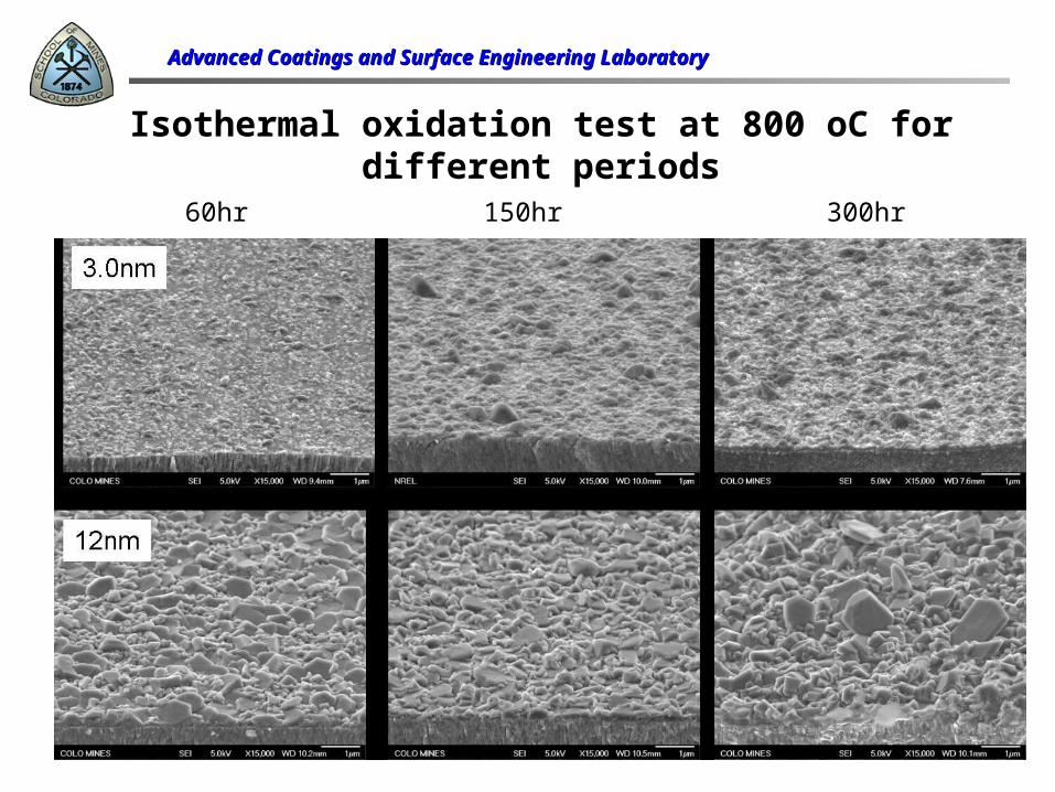
Isothermal oxidation test at 800 oC for different periods
60hr 150hr 300hr
Advanced Coatings and Surface Engineering Laboratory Advanced Coatings and Surface Engineering Laboratory
Isothermal oxidation test at 800 oC for different periods
60hr 150hr 300hr

Advanced Coatings and Surface Engineering Laboratory Advanced Coatings and Surface Engineering Laboratory
Hardness of CrN/AlN coatings measured after thermal annealing tests
0 200 400 600 800 1000 12005
10
15
20
25
30
35
40
45
Har
dn
ess
[GP
a]
Annealling temperature [ oC]
3.0 nm 12 nm Homo

Advanced Coatings and Surface Engineering Laboratory Advanced Coatings and Surface Engineering Laboratory
Sumarry
• CrN/AlN superlattice coatings exhibit further improved mechanical and wear resistance to the single layer CrAlN coatings
• CrN/AlN superlattice coatings also show excellent oxidation resistance both for high temperatures and long periods oxidation attack.
• Challenge: for complex shape dies (using MPP is a promising approach)

Advanced Coatings and Surface Engineering Laboratory Advanced Coatings and Surface Engineering Laboratory
Progresses in the work for AlN ‘smart’ coatings
• Dr. Fengli Wang has left ACSEL
• Ph.D. student Masood took over the research work on the development of AlN based ‘smart’ coatings.
• New Ph.D. student Ningyi Zhang will work on the other piezoelectric coating material LiNbO3 which is also a potential ‘smart’ coating candidate.

Advanced Coatings and Surface Engineering Laboratory Advanced Coatings and Surface Engineering Laboratory
MPP™ - An Alternative HPPMS/HiPIMS Technology
• Modulated Pulse Power - MPP™ – High power pulse magnetron sputtering technique– Heart of technology is the Zpulser™ plasma generator
Produces a multi-step DC pulse First step – ignition of low power discharge Second step – low power discharge Third step – transient stage from low power discharge to high
power discharge Forth step- high power discharge
Zpulser™ now at ACSEL

Advanced Coatings and Surface Engineering Laboratory Advanced Coatings and Surface Engineering Laboratory
MPP™ TechnologyModulated Pulse Power (MPP) Provides:
High ionization degree of metal species (see the plasma density)
high deposition rates (for both metal and insulating films)
Deposition of dense and uniform films
Easy scaling up (has moderate peak power, reduced cost)
Influencing film properties and structure by modulated pulse parameters (various controls)
2 4 6 8 10 12 14 16 18 20 22 24
40
60
80
100
120
140
160
180
200
220
240
Average Target Power Density [W/cm2]
Dep
osi
tion
Rate
[n
m/m
in]
MPP Cr DC Cr
The increase rate of the deposition rate
in MPP changes near 11-12 W/cm2
dc
MPP
Dc Cr
MPP Cr
The same power density on the target

Advanced Coatings and Surface Engineering Laboratory Advanced Coatings and Surface Engineering Laboratory
MPP System in ACSEL
Hiden electrostatic quadrupole plasma mass spectrometer (EQP)
Unbalanced magnetrons (100 mm x 280 mm)
MPP system and EQP plasma analyzer
Closed magnetic configuration
Zpulser MPP generator

Advanced Coatings and Surface Engineering Laboratory Advanced Coatings and Surface Engineering Laboratory
Plasma Characterization
• Hiden EQP mass-energy analysis– Compared conventional DC and MPP power with closed-field
unbalanced magnetrons• Only used one active magnetron
– Measured• Mass peak intensities
– 52Cr+1 (plus isotopes), 40Ar+1, and 26Cr+2
• Ion energy distributions– 52Cr+1, 40Ar+1, and 26Cr+2
EQP
Cr Al
N
N
S
S
N
S
14 cm
Closed Magnetic field
EQP
Cr Al
N
N
S
N
N
S
S
N
S
S
N
S
14 cm
Closed Magnetic field

Advanced Coatings and Surface Engineering Laboratory Advanced Coatings and Surface Engineering Laboratory
Comparison of DC and MPP Positive Ion Mass Scans52Cr+1
40Ar+1
52Cr+1
40Ar+1
26Cr+2
• Significant increase in the number of both target metal and gas ions for MPP than dc discharge
• Number of ions much greater for MPP than DC• In MPP, number of ions increased when average-peak power increased
DC sputtering Pave=3.5 kW
MPPTM sputtering Pave=3.5 kW

Advanced Coatings and Surface Engineering Laboratory Advanced Coatings and Surface Engineering Laboratory
Microstructure Comparison (DcMS, PMS, MPP)
fN2 =20-30%(h-Cr2N)
DcMS PMS MPP
fN2 =50-60%( c-CrN)
Zone-T columnar grains High density and fine grains High density and fine grains

Advanced Coatings and Surface Engineering Laboratory Advanced Coatings and Surface Engineering Laboratory
Wear Resistance
0 10 20 30 40 50 600.25
0.30
0.35
0.40
0.45
0.50
0.55
0.60
0.65
0.70
0.75
0.80
MPP CrN coatings (Floating bias) dc CrN coatings (-50V bias) PMS CrN coatings (-50V bias)
Coe
ffic
ien
t of
Fri
ctio
n
Nitrogen Flow Rate Percentage [%]
Pin-on-disc test
(3 N, 40 rpm, 5000 cycles, 1mm WC-Co ball)
The COF is lower in the MPP CrN coatings than in dc and PMS CrN coatings.

Advanced Coatings and Surface Engineering Laboratory Advanced Coatings and Surface Engineering Laboratory
Using Two Pulse Shapes• Working pressure: 5 mTorr• Nitrogen flow rate percentage: 40%• Two pulse shapes alternating (see the figures below) • Substrate bias: floating
700 s (6/6), 100 Hz rep rateDuration: 1S and 3S
1500 s (6/10), 30 Hz rep rateDuration: 1S and 2S
A
A

Advanced Coatings and Surface Engineering Laboratory Advanced Coatings and Surface Engineering Laboratory
Video showing Modulated Pulse Power Pulse

Advanced Coatings and Surface Engineering Laboratory Advanced Coatings and Surface Engineering Laboratory
Two pulse shapes with 1s Duration
700 s (6/6), 100 Hz rep rate 1500 s (6/10), 30 Hz rep rate
Denser structure with finer grains Properties:Hardness: 28.7131.615GPaYoung’s Modulus: 314.966 11.87GPaH/E ratio: 0.091COF: 0.25
0 1000 2000 3000 4000 5000 6000 70000.0
0.1
0.2
0.3
0.4
0.5
0.6
0.7
0.8
0.9
1.0
MPP CrN coating (11)
CO
F
Cycles
COF(ave)=0.25
Pave=0.8 kWDuration: 1S
Pave=3.5 kWDuration: 1S

Advanced Coatings and Surface Engineering Laboratory Advanced Coatings and Surface Engineering Laboratory
MPP Summary
• Excellent ionization of sputtered species (denser coating and excellent adhesion)
• High rate process (Cr coating depositions)
• Conducted EQP analysis of MPP and DC plasmas for closed-field UBMs– Number of ions increased when average-peak power increased
• Many more 52Cr+1 ions for MPP than DC
• Significant number of Ar ions
– Average energy for 52Cr+1 ions ~ 2eV• Very small high energy tail
• Almost mono-energetic source of ions
• MPP CrN coatings prepared at a floating substrate bias exhibited denser microstructure, comparable hardness and improved wear resistance to dc sputtered CrN coatings synthesized using -50 V dc substrate bias.
• MPP CrN coatings deposited using multiple pulse shapes exhibit further improved H/E ratio and wear resistance, where a low COF of 0.25 has been identified.