Embed Size (px)
Citation preview

ADVANCE INFORMATION Data Sheet No. PD60164A
IR1110
System Block Diagram
Product Summary
VDDS/VSS +/- 5V
ISS/IDD +/- 5mA
DC bus registration 100msec (typ.) response time
Min. DC bus regulation 35% of VDCMAX voltage with capacitive load
Programmable 100msec to DC bus ramp time 330msec (typ.)
SOFT START CONTROLLER ICFeatures• Self-contained soft charging of DC bus capacitor• DC bus voltage regulation• 3-phase or 1-phase AC input• Applicable to 115/230/380/460/575V AC input• Drives SCR phase controlled half bridge• Programmable ramp rate• Protection against DC bus short circuit• Fast power dip ride through with automatic ramp back• Selectable shutdown on single phase loss• 1-phase and 3-phase loss fault output• Insensitive to phase rotation• High line or low line fault output• Low power consumption• Integrated watchdog function for each phase• 64-pin MQFP package
DescriptionThe IR1110 is a high performance analog IC designedto control ramp rate and voltage of the DC bus fromeither single or three phase AC line voltage input. It con-trols a SCR half bridge and provides robust ride throughcapability in event of transient loss of line, and DC busregulation with eternal reference input. Comprehensiveline status fault output including 1/3 phase loss and highor low line fault provides versatile line diagnostic capa-bility to the system. The IR1110 is based on advancedlow power design so it can utilize the SCR snubberderived power supply.
Typical Application• Motor drives• Welders• Battery chargers• Power supplies
Snubber andSnubber der ived
power supp ly
(Opt ional )
a n dPer iphera l
C o m p o n e n t s
IR1110
A C3 - P h a s e
Input
+
-(Opt ional )
Package
64 Lead MQFP

2
IR1110 ADVANCE INFORMATION
www.irf.com
Symbol Definition Min. Max. UnitsVDD Positive supply voltage — 6.0
VSS Negative supply voltage — -6.0
VIN Operating input voltage range on UIN,VIN & WIN pins (VSS + 0.4) (VDD - 0.4)
VBIN Operating input voltage on VBOS and VBNEG - 4.5 3.0
VLED Operating input voltage on 1PHLED, LNLED, and LNLSLED pins — VDD
VLNSET Operating input voltage on LNSET — (VDD - 0.4)
ILED Sinking current on 1PHLED, LNLED, and LNLSLED pins — 3 mA
RthJA Thermal resistance, junction to ambient — 60
TA Operating ambient temperature -40 85
TJ Junction temperature — 150
TS Storage temperature -55 150
TL Lead temperature (soldering, 10 seconds) — 300
Absolute Maximum RatingsAbsolute maximum ratings indicate sustained limits beyond which damage to the device may occur. All voltage param-eters are absolute voltages referenced to AGND and DGND, all currents are defined positive into any lead. The thermalresistance and power dissipation ratings are measured under board mounted and still air conditions.
V
°C/W
°C
Recommended Component ValuesAll capacitors are rated 6.3V unless otherwise specified. All resistors are rated 1/16W unless otherwise specified. Thetypical connection diagram is shown in figure 3. For proper operation the device should be used with the recommendedcomponents specified below.
Symbol Definition Typ. Tolerance Units CommentsQU Phase U/V/W complementary MOSFET IRF7509 Complementary
QV NMOS/PMOS
QW Driver
RU1 Resistor divider for input voltage 3.4 X 1% kΩ Note 1
RV1 VACrms .25W
RW1 max
RB Bias resistor 249k 1%
RU2 Resistor divider for input voltage 9.09k 1%
RV2
RW2
RERR DC bus regulation error resistor 2M 5%
RCLAMP1 Ramp clamp resistor 1 430k 5%
RCLAMP2 Ramp clamp resistor 2 100k 5%
RRAMP Ramp resistor 82k 5%
Ω
3
IR1110ADVANCE INFORMATION
www.irf.com
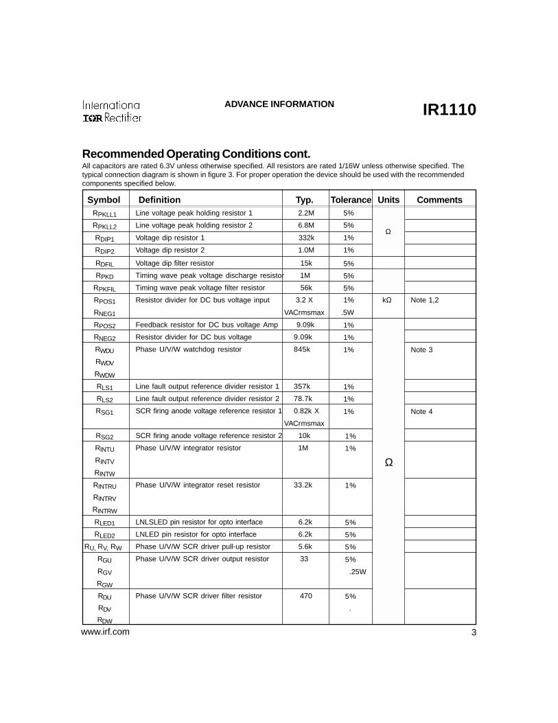
Recommended Operating Conditions cont.All capacitors are rated 6.3V unless otherwise specified. All resistors are rated 1/16W unless otherwise specified. Thetypical connection diagram is shown in figure 3. For proper operation the device should be used with the recommendedcomponents specified below.
Symbol Definition Typ. Tolerance Units CommentsRPKLL1 Line voltage peak holding resistor 1 2.2M 5%
RPKLL2 Line voltage peak holding resistor 2 6.8M 5%
RDIP1 Voltage dip resistor 1 332k 1%
RDIP2 Voltage dip resistor 2 1.0M 1%
RDFIL Voltage dip filter resistor 15k 5%
RPKD Timing wave peak voltage discharge resistor 1M 5%
RPKFIL Timing wave peak voltage filter resistor 56k 5%
RPOS1 Resistor divider for DC bus voltage input 3.2 X 1% kΩ Note 1,2
RNEG1 VACrmsmax .5W
RPOS2 Feedback resistor for DC bus voltage Amp 9.09k 1%
RNEG2 Resistor divider for DC bus voltage 9.09k 1%
RWDU Phase U/V/W watchdog resistor 845k 1% Note 3
RWDV
RWDW
RLS1 Line fault output reference divider resistor 1 357k 1%
RLS2 Line fault output reference divider resistor 2 78.7k 1%
RSG1 SCR firing anode voltage reference resistor 1 0.82k X 1% Note 4
VACrmsmax
RSG2 SCR firing anode voltage reference resistor 2 10k 1%
RINTU Phase U/V/W integrator resistor 1M 1%
RINTV
RINTW
RINTRU Phase U/V/W integrator reset resistor 33.2k 1%
RINTRV
RINTRW
RLED1 LNLSLED pin resistor for opto interface 6.2k 5%
RLED2 LNLED pin resistor for opto interface 6.2k 5%
RU, RV, RW Phase U/V/W SCR driver pull-up resistor 5.6k 5%
RGU Phase U/V/W SCR driver output resistor 33 5%
RGV .25W
RGW
RDU Phase U/V/W SCR driver filter resistor 470 5%
RDV .
RDW
Ω
Ω
4
IR1110 ADVANCE INFORMATION
www.irf.com
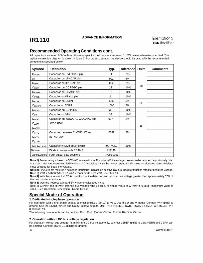
Special Mode of Operation1. Dedicated single phase operationFor operation with a one-phase bridge, connect 1PHSEL (pin12) to VSS. Use the U and V inputs. Connect WIN (pin3) toground. Use the SCRU (pin47) and SCRV (pin46) outputs. Use RPKD = 3.0MΩ, RWDU, RWDV = 1.0MΩ , CINTU,CINTV =0.0068υF 2%.The following components can be omitted: RW1, RW2, RWDW, CWDW, RINTW, RINTRW, CINTW.
2. Operation without DC bus voltage regulationFor operation without bus voltage, ie. maximum DC bus voltage only, connect VBREF (pin8) to VSS. RERR and CERR canbe omitted. Connect DCREGC (pin10) to ground.
Recommended Operating Conditions cont.All capacitors are rated 6.3V unless otherwise specified. All resistors are rated 1/16W unless otherwise specified. Thetypical connection diagram is shown in figure 3. For proper operation the device should be used with the recommendedcomponens specified below.
Note 1) Power rating is based on 550VAC rms maximum. For lower AC line voltage, power can be reduced proportionally. Vacrms max = Maximum operating RMS value of AC line voltage. Use the nearest standard 1% value to calculated value. Resistormust be rated for peak line voltage.Note 2) RPOS2 is not required if no series inductor(s) in place on positive DC bus. Resistor must be rated for peak line voltage.Note 3) VDD = 5.0V±2.5%. If 5.1V±2% zener diode sets VDD, use 866k 1%.Note 4) With these values LNLED is used for low line detection and is low at line voltage greater than approximately 57% ofVacrms maximum voltage.Note 5) Use the nearest standard 1% value to calculated value.Note 6) CRAMP and RRAMP sets the bus voltage ranp-up time. Minimum value of CRAMP is 0.68µF, maximum value is3.3µF. See Operation Description - Ramp Circuit.
Symbol Definition Typ. Tolerance Units CommentsCUVLO Capacitor on UVLOCAP pin .1 5%
C1PH Capacitor on 1PHCAP pin .001 5%
C3PH Capacitor on 3PHCAP pin .022 5%
CERR Capacitor on DCREGC pin .22 10%
CRAMP Capacitor on CRAMP pin 1.0 10%
CPKLL Capacitor on VPKLL pin .1 10%
CBDIP1 Capacitor on BDIP1 3300 5%
CBDIP2 Capacitor on BDIP2 1000 5%
CHOLD Capacitor on BDIPHLD .33 10%
CPK Capacitor on VPK .33 10%
CWDU Capacitor on WDCAPU, WDCAPV, and .027 2%
CWDV WDCAPW
CWDW
CINTU Capacitor between CINTU/V/W and .0082 2%
CINTV INTNU/V/W
CINTW
CU, CV, CW Capacitor in SCR driver circuit .0047/25V 10%
DRAMP Diode in series with RRAMP IN4148
Opto1,Opto2 Fault output opto couplers HCPL0701
µF
µF
PF

5
IR1110ADVANCE INFORMATION
www.irf.com
Symbol Definition Min. Typ. Max. Units Test ConditionsVDD Positive Supply Voltage 4.8 5.1 5.6 Note 3
VSS Negative Supply Voltage -4.8 -5.1 -5.6 Note 3
IDD VDD Supply Current —- 3.0 6.0 Note 4
ISS VSS Supply Current —- -3.0 -5.0 Note 4
VIN Input Voltage Range for UIN, VIN, and WIN 1.5 —- 4.0
VBREF Input Voltage Range for VBREF 0 —- 5.0 Note 1
VIL1 Input logic low voltage on 1PHEN, LNLSSL —- —- -2.0
VIH1 Input logic high voltage on 1PHEN, LNLSSL 2.2 —- —-
VPCINT Positive Output Voltage Swing at CINTU, CINTV, —- 4.0 4.5 Peak voltage of Vin
and CINTW Pins = 4.0V
VPCR+ Positive Output Voltage Swing at CRAMP Pin —- 4.0 4.5
VPCR- Negative Output Voltage Swing at CRAMP Pin 0 —- —-
I1PHCAP+ Sourcing Current at 1PHCAP pin —- 2.0 —- 1PHCAP=VSS
I1PHCAP- Sinking Current at 1PHCAP pin —- 5.0 —- 1PHCAP=GND
I3PHCAP+ Sourcing Current at 3PHCAP pin —- 3.0 —- 3PHCAP=VSS
I3PHCAP- Sinking Current at 3PHCAP pin —- 15.0 —- 3PHCAP=GND
VOLLED Output Low Voltage at 1PHLED, LNLSLED, and 0 0.12 .4 Output sinking
LNLED pins current = 3.0mA
VOHLED Output High Voltage at 1PHLED, LNLSLED, VDD —- VDD Output sourcing
and LNLSLED pin 0.4 current = 3mA
UVLO Undervoltage lockout between VDD-GND 4.1 4.4 4.6
IUVLO+ Sinking Current at UVLOCAP pin 60 86 110 uA VUVLOCAP=VDD
VHSCR Output Voltage at High level at SCRU, SCRV, —- 4.5 —- IO = 1mA
and SCRW pins
VLSCR Output Voltage at Low level at SCRU, SCRV, —- 0.1 0.31 IO = -1mA
and SCRW pins
VRAMPBUF Output Voltage at VRAMP pin —- 4.0 —-
RVBREF Input Resistance On VBREF pin —- 400 —- kΩ
IBDIPCAP Sourcing Current of BDIPCAP pin —- 5 —- uA BDIPCAP=VSS
VtLNLED+ Peak threshold voltage on UIN/VIN/WIN pins 2.2 2.3 2.4 VLNSET = 1.0Vfor LNLED to switch low
VtLNLED- Peak threshold voltage on UIN/VIN/WIN pins 2.0 2.1 2.2 Note 2for LNLED to switch high
VtLNLS Peak threshold voltage on UIN/VIN/WIN pins —- .5 —- All input voltagesfor LNLSLED to stay low present
Vt1PH Peak threshold voltage on UIN/VIN/WIN pins —- .5 —- All input voltagesfor 1PHLED to stay low present
DC Electrical CharacteristicsRBIAS = 249K/1%, VDD = 5.1V, VSS = 5.1V and TA = 25°C unless otherwise specified.
V
mA
V
µA
V
V
V
See notes on page 6

6
IR1110 ADVANCE INFORMATION
www.irf.com
See Notes on page 7
AC Electrical CharacteristicsVDD = 5.1V, VSS, = 5.1V, CL = 1000pF and TA = 25°C unless otherwise specified.
Symbol Definition Min. Typ. Max. Units Test Conditions
tr Turn-on rise time on SCRU, SCRV, and SCRW —- 500 —-
tf Turn-off fall time on SCRU, SCRV, and SCRW —- 500 —-
tWSCR Output pulse width of SCRU,SCRV, and SCRW —- 15 —- µs
tDLL LNLSLED propagation delay —- 30 —- LNLSSL=VDD,
C3PH =.022uF,
(note 1)
tD1PH 1PHLED propagation delay —- 8.3 —- ms C1PH = .001uF
tLN LNLED propagation delay —- 150 —- (note 2)
tS1PH Shutdown time after loss of single phase —- 15 20 ms 1PHEN = VDD,
CUVLO = .1mF,
C1PH = .001mF,
(note 3)
tfFO Fall time from high to low on LNLSLED, —- 50 —- ns Pull-up resistor
1PHLED, LNLED = 6.2kW
tW1PH 1PHLED pulse width —- 2 —- C1PH =.001mF,
(note 4)
tUVLCK Power up UVLOCK delay 60 msec CUVLCK=.1uF,
(note 5)
tRAMP DC bus ramp time 150 CRAMP=1uF,
RRAMP=82k,(note 6)
VENSCR Minimum input voltage on UIN, VIN, and WIN —- RU2/RU1 —- V (note 7)
for enabling SCR firing X 12
PPUBAL Phase-to-phase unbalance between —- ±1.5 —- Firing angle = 90°
pulses on SCRU, SCRV, and SCRW Notes 8 and 9
—- ±3 —- ° Firing angle = 140°
Note 9
ns
o
Notes for DC Electrical Characteristics
Note 1) VBREF=5.0V will assure full SCR firing on to produce the maximum amount of DC bus voltage and faster conver-gence to the maximum DC bus voltage. Although VBREF=4.0V corresponds to the maximum voltage, it will take longer timeto converge to the maximum DC bus voltage.Note 2) These voltage values are linearly proportional to VLNSET. For example, if VLNSET = 2.0V, then all values are twiceof those values listed in the table.Note 3) VDD must be regulated within ±2.5%. VSS must be regulated within ±5%.

7
IR1110ADVANCE INFORMATION
www.irf.com
Notes for AC Electrical Characteristics
Note 1) Delay is proportional to the capacitor values with minimum allowed value of C3PH = .01µFNote 2) Depends on CPKLL charge conditionNote 3) CUVLO = .1µF, C1PH = .001µF. Increasing CUVLO increases the delay/response time of the 1phase lockout.Note 4) Pulse width is proportional to C1PH. Maximum allowed values of C1PH is .001µF.Note 5) Power up delay is set by CUVLO or by VDD rise time whichever takes longer. In this condition, VDD rise time must
not be less than 100msec, and 1-phase shutdown must be enabled. If this is less than 100msec or 1-phase shutdown is disabled, CUVLO must be increased to 0.22µF in order to increase the undervoltage lockout time to greaterthan 100msec. See Note 3) above on additional effect of increasing CUVLO.
Note 6) Ramp time is proportional to the capacitor value.Note 7) This value corresponds approximately to 15V minimum SCR firing voltage. For 15V minimum SCR firing voltage,
(RSG2/RSG1) X VDD = (RU2/RU1) X 15.Note 8) PPUBAL applies to steady operation, is deviation of any firing point to closest balanced set of firing points.Note 9) Firing angle is defined with respect to zero delay (ie. max output voltage.
System Operating Characteristics and SpecificationsAll peripheral component values are those listed in the recommended operating condition unless otherwise specified.
Symbol Definition Min. Typ. Max. Units Test ConditionsVAC Line-to-line AC voltage range (1%) 80 120 140 Ru1,Rv1,Rw1=475K
RPOS1,RNEG1=453K
161 230 276 VRMS Ru1,Rv1,Rw19537K
RPOS1,RNEG1=887K
322 460 552 Ru1,Rv1,Rw1=2X953K
RPOS1,RNEG1=887K
fLINE Input line frequency 47 50/60 63 HzVBRANGE DC bus voltage controllable range 35 —- 99.8 % VBREF=1.4V to 4V
VBREG DC bus voltage regulation —- 2 —- %VBRES DC bus voltage step response time —- 100 —- msec VBUS=35% to 100%
Note 6tRAMP1 DC bus voltage ramp up time at power up — 150 —- msec CRAMP = 1µF
RRAMP = 82k(Note 7)
tRAMP2 DC bus voltage ramp up time at power dip —- 75 —- msec CRAMP = 1µFride through RRAMP = 82k
(Note 7)tdPWR Power up delay time before ramp up —- 190 —- msec CRAMP = 1µF
CUVLO = 0.1µFNote 9)
tdDIP1 Delay time to start ramp-up after recovery from 15 msec Voltage drop belowa transient loss of line voltage the reference voltage
at BDIP2 pinaFIRE Firing angle range 1.5 —- 160 ° Figure 2, Note 14
td1PHS Delay time to shutdown SCR firing pulses after 15 —- 30 msec 1PHEN = VDDloss of one phase input
td1PHE Delay time to start ramp-up after recovery from a —- 30 —- msec 1PHEN = VDDloss of one phase input

8
IR1110 ADVANCE INFORMATION
www.irf.com
Notes for System Operating Characteristics
Note 6) Step change of VBREF may result in excessive bus capacitor charging current. Rate of change of VBREF shouldbe decreased in order to limit bus capacitor charging current for practical application.
Note 7) Time to ramp up to 99.8% DC bus level at a power up. It does not include the power up delay time. The practicallimitation of the minimum time (50msec) depends on the inrush current to the DC bus capacitor. Ramp time isproportional to CRAMP.
Note 8) Time to ramp back to 99.8% DC bus level from 50% DC bus level at a momentary power dip. This does notinclude the delay time to start ramp-up (tDDIP)
Note 9) The value depends on CUVLCKNote 10) The value depends on CRAMP, RPK, RRAMPNote 11) The value depends on CRAMPNote 12) See operation description - Ramp CircuitNote 13) Firing angle defined with respect to fully off (zero output voltage) firing angle.Note 14) Firing angle defined with respect to zero delay.
td1FIRE First SCR firing angle at ramp-up — 20 32 ° CRAMP=1µF,RRAMP = 82k
(Note 10)16 25 ° CRAMP=2.2µF,
RRAMP = 47k(Note 10)
14 22 ° CRAMP=3.3µF,RRAMP = 30k
(Notes10,12, 13)RLIMFIRE Rate of advance of firing angle from last max firing —- 10 20° CRAMP = 1µF,
angle during ramp-up RRAMP = 82k 7 14 CRAMP=3.3µF,
RRAMP = 30k(Notes 11 and 13)
System Operating Characteristics and SpecificationsAll peripheral component values are those listed in the recommended operating condition unless otherwise specified.

9
IR1110ADVANCE INFORMATION
www.irf.com
Operating Mode/Fault Output Matrix ChartFault Fault output
Mode condition indicator Description External setting
Non- SCR output firing active. LNLSLED = low, LNLSSL = VDD
multiplexed 1PHLED = high 1PHEN = VDD or VSSNormal 1PHSEL = VDD
Multiplexed SCR output firing active. LNLSLED = low, LNLSSL = VSS1PHLED = high 1PHEN =VDD or VSS
1PHSEL = VDD Non- SCR output firing disabled for period of loss. LNLSSL = VDD
3-phase multiplexed LNLSLED = high, 1PHLED = high 1PHEN =VDD or VSS1PHSEL = VDD
loss Multiplexed SCR output firing disabled for period of loss. LNLSSL = VSSLNLSLED = high, 1PHLED = high (Note 1) 1PHEN =VDD or VSS
1PHSEL = VDDNon- SCR output firing active. LNLSSL = VDD
1-phase multiplexed LNLSLED = low, 1PHLED = toggles low for 1PHEN = VSS 3-phase loss 2msec once or twice per line cycle 1PHSEL = VDD
Input without Multiplexed SCR output firing active.LNLSLED toggles LNLSSL = VSS operation shutdown high while 1PHLED toggles low for 2msec 1PHEN = VSS
once or twice per line cycle. (Note 2) 1PHSEL = VDDNon- SCR output firing disabled for period of loss. LNLSSL = VDD
1-phase multiplexed LNLSLED = low, 1PHLED = toggles low 1PHEN = VDDloss for 2msec once or twice per line cycle 1PHSEL = VDDwith Multiplexed SCR output firing disabled for period of loss. LNLSSL = VSSshutdown LNLSLED toggles high while 1PHLED toggles 1PHEN = VDD
low for 2msec once or twice per line cycle. 1PHSEL = VDD(Note 2)
High/Low LNLED If line voltage exceeds the specified level on LNSET=desired voltage,AC line LNSET voltage, then LNLED = low. Otherwise 1PHEN =VDD or VSS
LNLED = high 1PHSEL = VDDNon- SCR output firing disabled for period of loss. LNLSSL = VDDmultiplexed LNLSLED = high, 1PHLED = high 1PHEN =VDD or VSS
1-phase 1PHSEL = VSS loss Multiplexed SCR output firing disabled for period of loss. LNLSSL = VSS
LNLSLED = high, 1PHLED = high 1PHEN =VDD or VSS1PHSEL = VSS
1-phase Non- SCR output firing active. LNLSLED = low. LNLSSL = VDD input multiplexed 1PHLED toggles low for 2msec once or twice 1PHEN =VDD or VSS operation Normal per line cycle 1PHSEL = VSS
Multiplexed SCR output firing active. LNLSLED toggles LNLSSL = VSShigh while 1PHLED toggles low for 2msec 1PHEN =VDD or VSSonce or twice per line cycle. (N ote 2) 1PHSEL = VSS
High/Low LNLED If line voltage exceeds the specified level on LNSET=desired voltage,AC line LNSET voltage, then LNLED = low. Otherwise 1PHSEL= VSS
LNLED = high 1PHEN =VDD or VSS
Note 1) LNLSLED may toggle high once for 2msec after event of phase loss.Note 2) 1PHLED and LNLSLED are completely synchronized and complementary.
uld
cticale is

10
IR1110 ADVANCE INFORMATION
www.irf.com
Functional Block Diagram
Line Sync&
Timing wavegenerator
Timing waveWatchdog
Timing waveReferenceGenerator
RampGenerator
C O M P
C O M P
RampClampAmp
Line VoltageProcessing
Vbus DipDetector
ErrorAmp
1 + s
1
ENABLE
R E S E T
-
-+
Fir ingvoltage
reference
3
33L INEV O L T A G E
V B U S
V B U SR E F
S C RFIR ING
P U L S E S3
Phase LossDetect
Single Phase
Line Loss
+
High/LowLine Faul t
3
τ
α
t ime
Vin
< 0 >
applied volts*seconds
Firing Angle,
Figure 1
Figure 2

11
IR1110ADVANCE INFORMATION
www.irf.com
Typical Connection Diagram
Figure 3
UIN VIN WIN
AV
SS
VB
AM
PP
VBAM
PN
VB
US
O
VB
RE
F
DC
RE
G2
DC
RE
GC
DC
RE
G1
1PH
SE
L
1PH
EN
LNLS
SL
1PH
CA
P
3PH
CA
P
AV
DD
VR
AM
P
RA
MP
ER
R
1 2 3 4 5 6 7 8 9 10
11
12
13
14
15
16
17
18
19
2 0
2 1
2 2
2 3
2 4
2 5
2 6
2 7
2 8
2 9
3 0
3 1
3 2
33
34
35
36
37
38
39
40
41
42
43
44
45
46
47
48
49
50
51
5 2
5 3
5 4
5 5
5 6
5 7
5 8
5 9
6 0
6 1
6 2
6 3
6 4CRAMP
RRAMP
RBIAS
VPKLL
UVLOCAP
AGND
AGND
BDIP2
BDIPCAP
BDIP1
BDIPHLD
DVSS
VINTDISC2
VP
KD
ISC
1
VP
K
VP
KR
EC
WD
CA
PW
WD
CA
PV
WD
CA
PU
LNS
ET
LNLS
LED
1PH
LED
LNLE
D
DG
ND
DV
DD
SC
RW
SC
RV
SC
RU
TES
T1
TES
T2
SC
RR
EF
AV
SS
AVDD
CINTW
INTNW
RINTW
RSTRW
CINTV
INTNV
RINTV
RSTRV
CINTU
INTNU
RINTU
RSTRU
IR1110M Q F P 6 4
Non Square
VSS
U
V
W
DC-
VDD
VDD
VDD
VDD
+15V
ToSCRs
VDD VDD
VBUSREF
D C +
R U R VR W
R G U R G V R G W
Q U Q V Q W
O P T O 1 O P T O 2
R S G 1
R S G 2
C I N T W
R I N T W
R I N T R W
C I N T V
R I N T V
R I N T R V
C I N T W
R I N T W
R I N T R W
R U 1
R V 1
R W 1
R N E G 1
R P O S 1
R P O S 2
R U 2
R V 2
R W 2
R N E G 2
R E R R
R C L A M P 1
C 1 P H
C R A M P
R C L A M P 2
C 3 P H
R R A M P
R B
R P K L L 2
C P K L L
C U V L O
R P K L L 1
C B D I P 2
R D I P 2C B D I P 1
C H O L D
R D F I L
R D I P 1
R W D W
R W D V
R W D U
R L S 1
R L S 2C W D U
C W D V
C W D W
C P K
R P K F I LR P K D
R L E D 1
R L E D 2
C E R R
R D U R D V R D W
C WC VC U
D R A M P
12
IR1110 ADVANCE INFORMATION
www.irf.com
Lead DefinitionsSymbol Pin # DescriptionDVDD 44 Logic positive supply voltage.DGND 43 Logic groundDVSS 31 Logic negative supply voltageAVDD 17 Analog positive supply voltageAGND 25,26,43 Analog groundAVSS 4,31,51 Analog negative supply voltageUIN/VIN/WIN 1,2,3 Phase U/V/W voltage inputsVBAMPP 5 DC bus OP Amp. positive input, connect to DC bus(-) via resistorVBAMPN 6 DC bus OP Amp. negative input, connect to DC bus (+) via resistorVBUSO 7 DC bus OP Amp. outputVBREF 8 DC bus regulation voltage reference inputDCREG2 9 DC bus error amplifier output via series diodeDCREG1 11 DC bus error amplifier outputDCREGC 10 DC bus error compensation (External capacitor connection pin)1PHSEL 12 Single phase input mode select. Note 1) on page 121PHEN 13 Single phase shutdown mode enable. Note 2) on page 12LNLSSL 14 Phase loss Fault Output Select. Note 3) on page 121PHCAP 15 Single phase loss detect timing capacitor3PHCAP 16 Three phase loss detect timing capacitorVRAMP 18 Buffered voltage ramp circuit outputRAMPERR 19 Ramp error amplifier inputCRAMP 20 Ramp timing capacitorRRAMP 21 Ramp timing resistorRBIAS 22 Bias current resistorVPKLL 23 Line-to-line peak voltage holding capacitorUVLOCAP 24 Under voltage lockout delay capacitorBDIP1 29 DC bus voltage dip detection 1BDIP2 27 DC bus voltage dip detection 2BDIPHLD 30 DC bus voltage dip hold capacitorBDIPCAP 28 DC bus voltage dip timing capacitorVPKDISC1 33 Line synchronization timing wave peak voltage discharging resistorVPKDISC2 32 No connectionVPK 34 Line synchronization timing wave peak voltageVPKREC 35 Line synchronization timing waveformWDCAPU/V/W 38,37,36 Watchdog timing capacitor for phase U, V, and WLNSET 39 Line voltage comparator reference inputLNLSLED 40 Line Loss Fault Output1PHLED 41 Single Phase Loss Fault OutputLNLED 42 High/Low line status OutputCINTU/V/W 61,57,53 Phase U/V/W integral amplifier outputINTNU/V/W 62,58,54 Phase U/V/W integral amplifier negative inputRINTU/V/W 63,59,55 Phase U/V/W integral amplifier resistor connectionRSTRU/V/W 64,60,56 Phase U/V/W integral discharge resistorSCRU/V/W 47,46,45 Phase U/V/W SCR gate signalTEST1 48 Test purpose pin (Should be tied to VDD)TEST2 49 Test purpose pin (No connection should be made)SCRREF 50 SCR gate signal reference

13
IR1110ADVANCE INFORMATION
www.irf.com
Lead Definitions
Note 1) 1PHSEL = VDD for 3 phase operation, 1PHSEL = VSS for 1 phase operation. See OperatingMode/Fault Output Matrix Chart for the detail.Note 2) 1PHEN = VDD for enable, 1PHEN = VSS for disable. See Operating Mode/Fault Output MatrixChart for the detail.Note 3) LNLSSL = VDD for total line loss only, LNLSSL = VSS for multiplexing total line loss/1 phase loss.See Operating Mode/Fault Output Matrix Chart for the detail.
Package Dimensions - 64 Lead MQFP
01-2023 01

14
IR1110 ADVANCE INFORMATION
www.irf.com
Operation Description
Overall Functional DiagramA detailed functional diagram of the IR1110 and peripheral components is shown in Figure 4.The IR1110 receives signals from the AC input lines U, V, W, and DC bus voltage, DC+, DC-, via
resistor dividers, and delivers line-synchronized pulses SCRU, SCRV, SCRW to external SCR gatedriver circuits. The timing of these pulses controls the DC bus voltage.
The IR1110 also delivers Status Feedback signals, that denote loss of all input phases, lossof one input phase and low/high AC line voltage.
The “ground” of the IR1110 is common with the SCR cathodes.
Line Voltage Processing circuit
The inputs to the line voltage processing circuit represent the voltage across the SCRs.Each of the three outputs of this circuit, RINTU, RINTV, RINTW is a voltage waveform that is
negative over the range of control of firing angle of the associated SCR, and positive outside thisrange.
The possible portion only of these waveforms appears at RSTRU, RSTRV, RSTRW.
Timing Wave IntegratorsEach Timing Wave Integrator integrates the negative portions of the output waveforms of
the Line Voltage Processing circuit, via RINT, and the positive portions, via RINT and RINTR inparallel.
The outputs, CINTU, CINTV, CINTW are a set of line synchronized “sawtooth” timingwaves. These have the desired phase relationship to the line voltages, so that intersection ofthese waves with the Timing Wave Reference defines the SCR firing instants. See Figure 5.
VPKL-L StoreVoltages UIN-VIN, VIN-WIN, WIN-UIN are rectified and the peak value, proportional to the
peak line voltage, is stored on CPKLL. The time constant of RPKLL1 and RPKLL2 with CPKLL allowsVPLL to track changes of line voltage that take place over a number of cycles, while maintaining anessentially smooth waveform.
WatchdogThe watchdog resets the Timing Wave Integrator within a few milliseconds of the normal
reset point, should an abnormality in the line voltage waveshapes, such as one or all input phasesmissing, prevent resetting at the normal time.
In the normal operation, the watchdog circuit plays only a passive role.

15
IR1110ADVANCE INFORMATION
www.irf.com
VPK StoreCPK stores a voltage, VPK, that is essentially equal to the peak of the timing waves. RPKD is
normally connected to ground via Q1. The time constant of RPKD with CPK allows VPK to trackchanges of amplitude of the timing waves that take place over a number of cycles, while maintain-ing an essentially smooth waveform.
Ramp CircuitThe current source, IRAMP, creates an increasing voltage, VRAMP, across CRAMP,
whenever Q3 has been conducting, then switches OFF. The maximum value of VRAMP isclamped at VPK.
VRAMP controls the ramp-up rate of the bus voltage. RRAMP shapes VRAMP to aparabolic form, which gives an approximately linear rise of DC bus voltage with a capacitive load.
The rate of change of VRAMP at the start of the ramp is set by CRAMP. RRAMP also hassome influence on the initial rate of change, but more influence later during the ramp-up period.
The greater the initial rate of rise of VRAMP, the greater the maximum first firing angle.Typical relationships between CRAMP,RRAMP,tDPWR, tRAMP1, and tD1FIRE are as follows:
CRAMP RRAMP tDPWR tRAMP tD1FIRE
uF kΩ (typical) (typical) (max) msec msec degrees
0.68 130 165 100 35
1 82 190 150 32 2.2 47 230 220 25
3.3 30 270 330 22
The minimum and maximum permissible values of CRAMP are 0.68uF and 3.3uF respectively. Totalramp-up time can be increased above the values shown by increasing RRAMP. For example, withCRAMP=3.3uF and RRAMP open, ramp-up time increases to about 1.2 seconds.
The maximum first firing angle is specified at maximum AC input voltage, and assumesthat worst case cumulative tolerances of the governing external components cause sufficientphase-to-phase unbalance that firing on one phase only occurs during the early part of ramp-up.
The circuit in Figure 15(a) will reduce the maximum first firing angle to 17°, if desired. Ifthe voltage regulation function is not used, and the circuit of Figure 13 is not used, the Figure15(b) circuit can be used in place of the Figure 15(a) circuit for the same purpose. With eithercircuit, both tDPWR and tRAMP will increase to about 400msec.
Ramp Clamp CircuitWhen Q4 is OFF, the ramp clamp is enabled, and Q3 is controlled by the output of the Ramp
Error Amplifier. This amplifier compares |VBUSO|, via RCLAMP1, with VRAMP, via RCLAMP2. The amplifiedoutput drives Q3 in a linear mode, diverting IRAMP from CRAMP and forcing VRAMP to be essentiallyequal to VBUSO x RCLAMP2/RCLAMP1.

16
IR1110 ADVANCE INFORMATION
www.irf.com
During transient line voltage outage, the Ramp Clamp is enabled. VRAMP is then forced intothe above relationship with VBUSO. The amplitude of VRAMP is thereby preset when the line voltagereturns, so that the bus voltage ramps back without significant delay, but also without unaccept-able jump of bus voltage.
The choice of RCLAMP2/RCLAMP1 is a compromise between the delay in starting ramp-backof the output voltage, and the initial jump of voltage when the line voltage returns after outage.
With an inductive filter at the output of the rectifier, RCLAMP2/RCLAMP1 can be set to a highervalue than with just a bus capacitor, to minimize the response time in restoring the DC bus voltageafter line outage.
Timing Wave Reference Summing AmplifierThe output of the Timing Wave Reference Summing Amplifier is the Timing Wave Refer-
ence; this is essentially the difference between VPK and VRAMP, so long as the output of ErrorAmplifier 2 is zero. Thus, when VRAMP is zero, the Timing Wave Reference voltage is essentiallyequal to VPK, and SCR firing angle is close to the zero crossing of the line-to-line voltage; as theramp increases, the firing angle advances. Refer to Figure 5.
Closed Loop Bus Voltage RegulationThe bus voltage reference, -VBUSREF, sets the amplitude of the steady bus voltage. This
external reference is negative with respect to “ground”, i.e., with respect to the positive outputterminal of the rectifier bridge. This facilitates derivation of VBUSREF, if required, via a level shiftcircuit that is referenced to the negative DC bus.
If bus voltage control is not used, and steady operation at the maximum DC bus voltageonly is required, VBUSREF should be connected to VSS.
The Inverting Amplifier inverts the reference to +VBUSREF. If the maximum possible valueof |VBUSO| is less than |VBUSREF|, the voltage regulation loop is inactive. The average output ofError Amplifier 1 is always negative, the voltage across CERR is clamped to zero by the paralleldiode, the output of Error Amplifier 2 is always zero, and the bus voltage ramps to the maximumpossible value.
If |VBUSO| becomes greater than |VBUSREF|, the average output of Error Amplifier 1 becomespositive. This output is filtered by RERR and CERR, and a smooth voltage representing the dc errorbetween |VBUSO| and |VBUSREF| appears across CERR. This voltage is amplified by Error Amplifier 2,and fed as an input to the Timing Wave Reference Summing Amplifier. The added input to theTiming Wave Reference Summing Amplifier increases the Timing Wave Reference, delaying theSCR firing angle, and forcing the bus voltage to a value proportional to |VBUSREF|.
Since the voltage regulation circuit becomes active only when |VBUSO| exceeds |VBUSREF|,the ramp rate during power-up of the bus voltage is determined solely by the rate of increase ofVRAMP. If |VBUSO| starts to exceed |VBUSREF| during ramp up, the output of Error Amplifier 2 starts tooppose the increasing ramp voltage, restraining further increase of bus voltage. Some overshootoccurs while the ramp continues to increase to VPK.
In normal operation, after ramp up, the bus voltage is no longer controlled by the ramp,unless an event occurs that causes the ramp to be clamped.
Rise and fall rates of the bus voltage that are driven by changes in |VBUSREF| in normaloperation are determined by the applied rise and fall rates of |VBUSREF|, and by the characteristics

17
IR1110ADVANCE INFORMATION
www.irf.com
of the load connected to the DC bus. The rate of increase of applied |VBUSREF| should be limited ifnecessary, to limit the bus capacitor charging current.
Adjustment of DC loop gainThe voltage regulation loop may exhibit uneven firing angle from one SCR to the next, with
loads which have unusually high ripple voltage. Such ripple instability, if it occurs, can be corrected byreducing the DC loop gain. Figure 6 shows how this is done with a voltage divider, R1 and R2, in thevoltage regulation loop.
SCR Timing ComparatorsEach SCR Timing Comparator delivers a high output whenever the Timing Wave is instanta-
neously greater than the Timing Wave Reference. The leading edge is the demanded initiation pointfor the SCR firing pulse.
The duration of the output pulse of the SCR timing comparator is generally much longer thanneeded to fire the SCR, because the Timing Wave remains higher than the Timing Wave Referencefor a significant portion, if not all, of the total cycle time. See Figure 5.
SCR Voltage ComparatorsEach SCR Voltage Comparator compares the instantaneous anode-cathode voltage of the
SCR with a fixed reference, SCRREF, which is set by RSG1 and RSG2. This reference is set to repre-sent an actual anode-cathode voltage of about 15V, before attenuation through the input dividerresistors.
When the instantaneous SCR anode voltage is greater than 15V, the output of the SCRVoltage comparator is high. The outputs of the SCR Voltage and Timing Comparators are ANDed toobtain the output SCR timing pulses, SCRU, SCRV, SCRW.
The SCRU, SCRV, SCRW output pulses are thus controlled so that; a) they do not occur when the Timing Wave is less than the Timing Wave Reference b) they do not occur unless the instantaneous SCR voltage is at least 15V positive c) they are terminated when the instantaneous anode-cathode voltage falls below 15V; -i.e. as soonas the SCR turns on
With discontinuous output current, more than one firing pulse per cycle for each SCR may begenerated.
The pulse width of SCRU, SCRV, SCRW is about 6usec at maximum output voltage, andabout 13usec at reduced output voltage.
SCR Gate DriversThe SCR gate driver circuit, shown in Figure 7, amplifies and stretches the SCRU, SCRV,
SCRW timing pulses. C1 and R2 stretch the duration of the output pulse to 60-80usec. This isgenerally necessary to ensure reliable SCR turn-on.
C2 and R4 provide an initial peak turn-on firing current of about .45A, decaying to about .2Awithin 5usec. The maximum average current consumed by the three SCR driver circuits is about10mA.
If C2 and R4 are omitted, the peak firing current will be reduced to about .2A. R3 can bedecreased to say 33W, to restore the peak firing current to .45A; the maximum average supplycurrent will now increase to about 20mA.

18
IR1110 ADVANCE INFORMATION
www.irf.com
Voltage Dip CircuitThe DC bus voltage will fall if the input line voltage dips or is lost.For short period outage, the bus capacitor voltage may hold up sufficiently that ramp back
when the line voltage returns is unnecessary.If the bus voltage falls below a preset level, then the ramp is automatically clamped, in
order to avoid an unacceptable jump of bus voltage when the line returns.The Voltage Dip Comparator monitors dips on the DC bus voltage. The bus voltage, -
VBUSO, is captured on CHOLD. The Voltage Dip Comparator compares a fraction of this capturedvoltage, with -VBUSO.
In normal operation, |kVBUSO| is less than |VBUSO|, and the output of the Voltage DipComparator is high. When a short line outage occurs, the voltage captured on CHOLD remainssubstantially equal to the pre-dip value, while |VBUSO| starts to decrease as the bus capacitordischarges. If |VBUSO| dips to less than k x VBUS1, where VBUS1 is the initial bus voltage, the outputof the Voltage Dip Comparator latches low, Q4 is switched off and the ramp is clamped. Q5 isturned ON, discharging the voltage on CERR.
RDIP2
kVBUS1 = x VBUS1 - (0.1 VLLMAX) RDIP1 + RDIP2
where VLLMAX is the maximum design value of rms line voltage
The Voltage Dip Comparator remains low for a minimum period, TDELAY2, of approxmately 5milliseconds, set by CBDIP1. Thereafter, so long as the line voltage is absent or remains abnormallylow, the output of the Timing Wave Intersect Comparator remains low, keeping the Voltage DipComparator latched low.
TDELAY2 in milliseconds is approximately equal to (.0015 X CBDIP1 pF). Thus for CBDIP1 =3300pF, TDELAY2 is about 5 milliseconds.
The total delay, TDELAY_TOT, between the point of initiation of the line voltage outage, andthe point at which the voltage dip comparator is allowed to reset, must be at least 10 milliseconds.
TDELAY_TOT is the sum of TDELAY1 and TDELAY2. TDELAY1 is the time between the point ofinitiation of the line outage, and the point at which the bus voltage falls to kVBUS1. Thus, withTDELAY2 set at 5 milliseconds, the minimum allowed value for TDELAY1 is 5 milliseconds.
If the bus capacitor is sized so that, at maximum DC load current, the bus voltage will fallto kVBUS1 in less than 5 milliseconds, then CBDIP1 should be increased to ensure that TDELAY_TOT
cannot fall below 10 milliseconds.If CBDIP1 is increased so that TDELAY2 is at least 10 milliseconds, TDELAY_TOT will always be
greater than 10 milliseconds. This is an inherently safe design approach, though it does add a fewmilliseconds of potentially unnecessary delay, before ramp-back can commence during a shortline outage.

19
IR1110ADVANCE INFORMATION
www.irf.com
After the above delay, the Voltage Dip Comparator is reset when the output of the TimingWave Intersect Comparator goes high, which occurs when the line voltage returns to normal. Q2is momentarily turned ON, allowing the voltage on CHOLD to reset. Q4 is turned ON, unclampingthe Ramp, and Q5 is turned OFF, unclamping CERR. Ramp-back of the bus voltage now occurs.
When the output of the Voltage Dip Comparator is low, Q1 is turned OFF. RPKD is thendisconnected from ground, allowing CPK to hold its charge during the voltage dip.
Voltage Dip during Dynamic RegulationIf |VBREF| is rapidly decreased by a sufficient amount, this may cause a decrease of bus
voltage that will set the Voltage Dip Comparator and cause the bus voltage to undershoot.Since the timing waves are still present, the output of the Timing Wave Intersect Com-
parator remains high, and the Voltage Dip Comparator will be quickly reset, ramping the busvoltage back to the set value.
This undershoot of the bus voltage will be avoided if changes in |VBUSREF| are controlled ata rate that does not significantly “overtake” the discharge rate of CHOLD, which is set by CHOLD,RDIP1 and RDIP2.
Undervoltage and Undervoltage Lockout ComparatorsThe UV Comparator delivers a high output when VDD exceeds the internally fixed
reference value.The UV Lockout Comparator delivers a high output when the voltage CUVLO exceeds a
nominal value of about 1.5V. CUVLO is driven from a current source of approximately 2uA.The outputs of the UV and UV Lockout Comparators are ANDed. When the output of
either comparator is low, the SCR firing pulses are inhibited, and Q4 is turned OFF, clampingthe ramp.
One Phase Loss CircuitA train of fixed duration (nominal 2msec) pulses are delivered to the gate of Q6, if one
input phase is missing. With 1-phase shutdown enabled, each 1-phase loss pulse dischargesCUVLO by about 1.5V. During the third successive pulse, CUVLO is discharged sufficiently that theoutput of the UV Lockout Comparator goes low.
The principle of generation of the 1-phase loss pulses is illustrated in Figure 8. Thesepulses are generated; (a) during one phase loss (b) briefly during abnormal dips of line voltage (c) if the DC bus is short circuited and the SCR firing angle is advanced by more than about 30°from the zero crossing of the line voltage
With 1-phase shutdown enabled, generation of “1-phase loss” pulses under condition (b)reinforces the ramp clamp function. Under condition (c) it results in automatic limiting of shortcircuit current, as explained later.
The 1-phase loss pulses at 1PHLED output follow the output of the 1-Phase Loss Circuit.

20
IR1110 ADVANCE INFORMATION
www.irf.com
Line Loss CircuitThe output of the line loss detection circuit is high in normal operation. If all input phases
are lost, it goes low, after a delay, determined by C3PH, which would typically be set to about 2cycles.
When the output of the Line Loss circuit goes low, Q1 is turned OFF. This disconnectsRPKD from ground, allowing CPK to hold its charge during the line outage.
The output of the line loss circuit feeds via NAND 2 to the LNLSLED output driver. IfLNLSSL is connected to VSS, the 1-phase loss pulses are multiplexed with the output of the lineloss circuit at the LNLSLED output. If LNLSSL is connected to VDD, the LNLSLED signal signifiesloss of all input phase only.
Line Voltage ComparatorThe output of the Line Voltage Comparator is low when VPKLL exceeds a reference value
that is set by RLS1 and RLS2. The LNLED output follows the output of the Line Voltage comparator.
PWM Control of VBUSREF
VBUSREF can be controlled by Pulse Width Modulation (PWM). The IR1110 responds onlyto the average value of this waveform; suitable PWM frequency is in the range of one to severalkHz.
Figure 9 shows an opto-coupler circuit for transmitting an isolated PWM input.Control of the ON/OFF duty cycle of the opto-transistor, from 0 to 100%, controls the
average value of VBUSREF from VMIN to VMAX, where;
R1
VMIN = VSS
R1 + R2
R1
VMAX = VSS
R1 + R’
R2R3
R’ = R2 + R3
The average value of VBUSREF(D) at duty cycle D is:
VBUSREF(D) = VMIN + D(VMAX - VMIN)
As an example, if VSS = -5.0V, R1 = 7.32k, R2 = 16.9k, R3 = 1.91k, then the average value ofVBUSREF will be controlled from approximately -1.5V to -4.0V, corresponding to a range of controlof the bus voltage from 37.5% to 100% of the maximum value at maximum operating line voltage.

21
IR1110ADVANCE INFORMATION
www.irf.com
Dedicated One Phase OperationThe IR1110 can be set for dedicated operation of a 1-phase half-controlled SCR bridge.
The UIN and VIN input terminals are used. No connection is made to WIN.When Pin 12 is connected to VSS, the W timing wave and watchdog circuits are disabled,
the watchdog reset time is optimized for 1-phase operation, and 1-phase shutdown is disabled,regardless of the connection of Pin 13.
Snubber Derived Power SupplySnubbers will generally be required, either across the AC lines or directly across the
SCRs, to limit dv/dt when the line voltage is switched on.If SCR snubbers are used, the snubber current can be used to derive the power supply
voltages for the IR1110 and SCR drivers.With reference to Figure 10, positive snubber current flows via the three RC snubbers and
the D+ diodes, to create a nominal 15V supply across ZD1 and C1, for the SCR driver.A nominal positive 5.1V VDD supply is developed across ZD2 and C2. Negative snubber
current flows via D- diodes, to create a nominal -5.1V VSS supply across ZD3 and C3.The ZD1 and ZD4 protect the supply voltages against transients on the line voltages.This power supply circuit requires that the average current consumed by the SCR driver
circuits does not exceed about 10mA.Note that an auxiliary winding on a DC bus derived switching power supply would not by
itself serve the IR1110. This is because bus-derived power cannot deliver voltage until aftercharging of the DC bus capacitor has already commenced, while the IR1110 must be poweredbefore charging of the bus capacitor commences.
It would be possible to use an auxiliary winding on a DC bus derived power supply tosupplement the snubber derived power. This could be preferred where the AC input line induc-tance is high, therefore only minimal snubbers - insufficient to furnish the total power required bythe IR1110 and SCR drivers - are needed for dv/dt protection of the SCRs.

22
IR1110 ADVANCE INFORMATION
www.irf.com
Figure 4 Detailed Functional Block Diagram
Watch -Dog
Line Vo l t ageP r o c e s s i n g
Ci rcu i t
1
2UIN3VIN
WIN
U V W
R U 1
R V 1R W
1
R W2
R V 2R U 2
D E L A Y
LINEL O S S
CIRCUIT
1PHASEL O S S
CIRCUIT
D C +
D C -
6 3 , 5 9 , 5 5 RINTU,V,W
6 4 , 6 0 , 5 6
R S T R U , V , W
CINTU,V,W
6 1 , 5 7 , 5 3
W D C A P U , V ,W
3 6 , 3 7 , 3 83 5
V P K R E C 3 4
CINTU,V,W
V P K
C P K
RP
KD
3 3
R P K L L 1
C P K L L
2 3
R P K L L 2
V D D
R S C 1
R S C 2
5 0S C R V O L T A G EC O M P A R A T O R
S C R R E F
SCR T IMINGC O M P A R A T O R
A N D 1
A N D 2
V D DU V C O M P A R A T O R
U V L OC O M P A R A T O R
R L S 1
R L S 2
3 9
V D D V D D
L N L E D
4 2
S C R U , V , W
4 5 , 4 6 , 4 7
1 P H L E D
4 1
V D D
V D D
L N L S L E D
4 0
N A N D 2
1 P H C A P
1 5
C 1 P H
U V L O C A P2 4
CU
VLO Q 6
1PHEN
1 3
1 63 P H C A P
C 3 P H
L N L S S L
1 4
T IM ING WAVE INTERSECTC O M P A R A T O R
TIMING WAVEREF SUMMING
A M P
3PH/1PHC O M P A R A T O R
A N D 3
A N D 4
R A M PE R R O R A M P
R C L A M P 2
R C L A M P 11 9
R A M P E R RV R A M P
1 8
R A M PB U F F E R A M P
2 1R R A M P
C R A M P
2 0
C R A M P
R R A M P
Q 3
R P O S 2
R P O S 1
R N E G 1
6
5
RN
EG
2
V B U S O7
BDIP12 9
V B R E F
8
BDIPHLD
3 0
RD
IP1
RD
IP2
BD IP22 7
Q 5
V O L T A G E D I PC O M P A R A T O R
R E S E T
D C R E G 29
E R R O RA M P 1
( INVERTING)
INVERTINGAMPLIF IER
R D F I L
2 8
C B D I P 1
N A N D 1
E R R O RA M P 2
(NON- INVERTING)
B D I P C A P
R E R R
1 1 1 0D C R E G C
C E R R
D C R E G 1
Q 4
Q 2
Q 2
Q 1
INTNU,V,W5 2 , 5 3 , 5 4
T i m i n g W a v eIn tegra to r R P K F I L
V P K L L
C B D I P 2
CH
OLD
IRAMP
L I N E V O L T A G EC O M P A R A T O R
L N S E T
23
IR1110ADVANCE INFORMATION
www.irf.com
U V W U V W
W
V
U
SCR T imingComparator
Output
U,V,W T imingWave fo rms
Timing WaveReference =
V - VRAMPPK
Figure 5 Timing Waveforms, Timing Wave Reference SCR Timing Comparators
Figure 6 Circuit for Reducing the DC loop gain
D C R E G 1PIN 11
D C R E G CPIN 10
R E R R
C E R RR 2
R 1
D C L O O P G A I N R E D U C E D B Y
R2/ (R1 + R2)
R1 + R2 = 200k ohms approx .

24
IR1110 ADVANCE INFORMATION
www.irf.com
INPUTs to3 P H / 1 P H
Compara to r
NORMAL 3-PHASE OPERATION
(a) LOSS OF ONE INPUT PHASE
Outpu t o f1 -Phase Loss C i rcu i t
< 0 >
INPUTs to3 P H / 1 P H
Compara to r
< 0 >
Outpu t o f1 -Phase Loss C i rcu i t
+12 .5 to +15V
S C R US C R VS C R W
4 7 01 / 1 6 W
5.6K1 / 1 6 W
0.0047uF2 5 V
C 1 R 2
R 1
1
R 4C 2
5 6 1 / 8 W
4 3 1 / 8 W.1uF 25V
S C R G A T EU , V , W
7,8
5,6
34
32IRF7509
O P T I O N A L
Figure 7 SCR Gate Driver Circuit
Figure 8, 8(a) Principle of Generation of 1-Phase Loss Pulses

25
IR1110ADVANCE INFORMATION
www.irf.com
INPUTs to3 P H / 1 P H
Compara to r
(b) ABNORMAL DIP OF LINE VOLTAGE
(c) DC BUS SHORT CIRCUIT. FIRING ANGLE 30 ADVANCED
Outpu t o f1 -Phase Loss C i rcu i t
< 0 >
INPUTs to3 P H / 1 P H
Compara to r
< 0 >
Outpu t o f1 -Phase Loss C i rcu i t
Figure 8(b), 8(c) Principle of Generation of 1-Phase Loss Pulses

26
IR1110 ADVANCE INFORMATION
www.irf.com
480V AC3-Phase
Input
+12.5 to +15V
-5.1V
+5 .1V
D+D+
D+ D-
D-D-
UVW
D C -
D C +
.15uF1200V
.15uF1200V
.15uF1200V
1001 0 W 100
1 0 W 1001 0 W
1N4004
15V1 W5 %
Z D 1 C 1
100uF
150 1 /10W
220 1/4W
Z D 51 N 5 2 3 1 C
C 2330uF6.3V
C 3330uF6.3V
Z D 21 N 5 2 3 1 C
Z D 31 N 5 2 3 1 CZ D 4
6.8V .5W5 %
751 /10W
Note: For 240V input,snubber capacitor = .33uF/600V
snubber resistor = 10 2W
Figure 10 Snubber Derived Power Supply
Figure 9 Circuit for PWM Control of DC Bus Voltage
P W M I N P U TR 2
R 1
8
5
2
6
3
TOV B U S R E F
PIN8 o fIR1110
R 3
V S S
HCPL0453
27
IR1110ADVANCE INFORMATION
www.irf.com
T 0 T 1 T 2 T 3 T 4
4.0V
-4.0V
11.0V min
AC L INEV O L T A G E
V S S
V D D
< 0 >
SCR Dr i ve rSupp l y
1 .0msec < T0 - T1 < 80msec100msec < T1 - T2T3 - T4 < 40msecVSS should track VDD within +/-10% dur ing r ise/ fal l t ime
Note: T4 is the event of Undervol tage Lockout
Figure 11 Power Supply Requirement
2 2 0 K 5 % 1 / 1 6 W
R 12 7 K 5 %
1 / 1 6 WR 2
2 4 K 5 %
1 / 1 6 W
4 7 K 5 % 1 / 1 6 W
C 1.1uF
Q 12 N 4 4 0 1
Q 22 N 4 4 0 1
TOU V L O C A P
(PIN24IR1110)
TO1 P H L E D(PIN41
IR1110)
T O L N L E D(PIN42
IR1110)
TOL N L S L E D
(PIN40IR1110)
L O S S O FL INE
S H U T D O W NCIRCUIT
L O W L I N ES H U T D O W N
CIRCUIT
N O T E S :(1 ) I f P in14 to VDD, use CUVLO=.1uF and omi t D1 ,R2(2) I f P in14 to VSS, use CUVLO=.22uF and omi t C1 ,D1,R2(3) I f power supp ly r i se t ime < 80msec (F igure 11) , connec t p in 14 to VSS, use CUVLO=.22uF, and omi t C1,D1,R2.(4) I f F igure 13 c i rcu i t i s used. Connect p in 14 to VDD. Use CUVLO=0.22uF and R1=0.(5 ) Se t RLS1, RLS2 fo r LNLED low above 85% o f m in opera t ing vo l tage
D 11 N 4 1 4 8
Figure 12 Loss of Line and Low Line Shutdown Circuits

28
IR1110 ADVANCE INFORMATION
www.irf.com
VDD
4 7 0 K5 %
1 / 1 6 WR 2
R 1
4 7 0 K5 %
1 / 1 6 W .1uF1 0 %
2 N 4 4 0 1
Q 1
2 N 4 4 0 1
Q 2
R 34 7 K5 %
1 / 1 6 W
TOPIN24IR1110
TO PIN11IR1110
( E R R O R A M P 1 O U T P U T )
NOTE:( 1 ) R e m o v e C E R R a n d R E R R(2) Connect P IN10 o f IR1110 to GND
(3) Se t VBUSREF = -VL INEMIN X 3 .4
V L I N E M A X
(4) P IN13 connec ted to VDD to enab le1-phase shu tdown a t low bus vo l tage
Figure 13 Circuit for Enabling 1-Phase Shutdown During Ramp-Up, Disabling DuringNormal Operation (Bus Voltage Control Function Not Used)
86
2
3
5 H C P L 0 4 5 3
1 0 m A t o c l a m p VRAMP to zero
To p in6 o f IR1110
4 .7K
V S S
Figure 14 Circuit for Externally Clamping VRAMP to zero
29
IR1110ADVANCE INFORMATION
www.irf.com
V D D
V S S
To PIN20 IR1110( C R A M P )
1 9 1 k 1 % 1 / 1 6 W
1 M 1 % 1 / 1 0 W
To PIN7 IR1110
To PIN20 IR1110( C R A M P )
V D D
2 N 4 4 0 1
2 N 4 4 0 1
4 7 0 k 5 % 1 / 1 6 W
To PIN11 IR1110
No te 1 ) Use CRAMP = 0 .33uF
No te 1 ) Use CRAMP = 0 .33uF 2 ) Remove CERR and RERR 3 ) Connect PIN10 IR1110 to ground 4 ) Set VBUSREF = -0 .8V
b)
a)
1 0 0 k 5 %1 / 1 6 W
1 2 0 k 5 % 1 / 1 6 W
1 0 0 k 5 % 1 / 1 6 W
1 2 0 k 5 %1 / 1 6 W
I R L M L 2 8 0 3
0 .1uF1 0 %
1/2 LM2903
Figure 15 Circuits for reducing tD1FIRE

30
IR1110 ADVANCE INFORMATION
www.irf.com
Operating Scenarios and Design Options
Power Supply Response CharacteristicsThe UV comparator responds to the amplitude of the VDD supply, to control the ramp clamp.In order to correctly accomplish this function, the power supply should have the response
characteristics illustrated in Figure 11, and 1-phase shutdown must be enabled. A minimum risetime of 100msec during initial power-up is required to provide sufficient delay time, before theoutput of the UV comparator goes high, for VPK to become established before ramp-up commences.
During loss of line voltage, VDD should not hold up above 4.0V for more than 40msec, toensure timely clamping of the ramp via the UV comparator.
The snubber derived power supply in Figure 10 has the required rise time, however hold-up time exceeds 40msec. Timely clamping of the ramp can instead be accomplished by theexternal Loss of Line Shutdown circuit, described below.
If 1-phase shutdown is disabled, the rise time of VDD must be increased to about200msec to control the ramp clamping function. In this case it may generally be better to controlthe ramp clamp via the UVLO comparator, by increasing CUVLO to 0.22uF. The rise time of VDDis no longer critical, and can have a minimum value of 1msec.
Loss of Line Shutdown circuitsThe Loss of Line Shutdown circuit in Figure 12 clamps the ramp during line outage, via
the Undervoltage Lockout Comparator.The Note (3) option of Figure 12 also eliminates dependence on a minimum power supply
rise time of 80msec. CUVLO is increased to 0.22uF, to provide sufficient delay during power-up, viathe UVLO Comparator. The rise time of the power supply is not now critical, and can have aminimum value of 2.0msec.
A side effect of increasing CUVLO is to increase the shutdown time when one phase is lost.With Pin 14 connected to VSS, this is corrected by Q1 being turned on during each 1-phase losspulse, which adds to the discharge current for CUVLO, via R1.
Low Line Shutdown circuitThe Low Line Shutdown circuit in Figure 12 clamps the ramp and removes the SCR firing
pulses if the line voltage falls to less than 85% of the minimum normal operating level. This circuitmay not be necessary for all applications, but its inclusion will provide added insurance of correctoperation during abnormal low line conditions.
Loss of one phase during three phase operationThe 1-Phase Shutdown circuit clamps the ramp and removes the SCR firing pulses if one
input phase is lost for more than about one cycle. When the missing phase returns, the ramp isunclamped and the bus voltage ramps back to the set value.
If 1-Phase Shutdown is disabled, the IR1110 will continue to deliver DC bus voltage whenone input phase is lost. A potential problem arises, however, if the bus voltage is being regulatedsignificantly below the maximum value. If one phase is lost and the ramp remains unclamped formore than one or two cycles, when the missing phase returns the bus voltage may transientlyjump to almost the maximum possible value, before it is regulated back to the set value. This can

31
IR1110ADVANCE INFORMATION
www.irf.com
result in excessive bus capacitor charging current.For this reason it is recommended that the 1-Phase Shutdown circuit is enabled, (Pin 13
connected to VDD) in designs where the voltage control function of the IR1110 is used.For designs where the voltage control function is not used, operation at full bus voltage,
with 1 Phase Shutdown disabled, allows natural transitioning from 3-Phase to 1-Phase operation,and vice versa, without excessive voltage jumps.
With 1-Phase Shutdown disabled, however, transient loss of one phase, during the earlypart of ramp-up, could cause a jump of bus voltage and a high instantaneous bus capacitorcharging current, if the missing phase returns before ramp-up has finished, while the instanta-neous bus voltage is still low.
The likelihood is remote of one phase being lost and then returning during the infrequentlyoccurring first 50 to 100ms window of the initial ramp-up period. Given the improbability of such anevent, provided the instantaneous charging current cannot exceed the surge capability of theSCRs, no additional remedy may generally be necessary.
The circuit shown in Figure 13 can be used to protect against this unlikely event, if judgednecessary. The polarity of the Error Amplifier 1 average output signifies whether the instantaneousbus voltage is above or below a fixed level, set by VBREF.
If one phase loss occurs during ramp-up, when the bus voltage is instantaneously belowthe set level, the output of Error Amplifier 1 is negative, and Q2 is ON, 1-Phase Shutdown isenabled. If one phase loss occurs at instantaneous bus voltage above the set level, Q2 is OFFand the voltage on CUVLO is pulled high by R3, disabling 1-Phase Shutdown.
DC bus Short CircuitWith a short circuit across the DC bus, the line-to-line voltages collapse to zero at the
SCR firing instants, causing the timing waves to terminate prematurely.If a short circuit is present at start up, 1-phase loss pulses start to be generated as the
ramp increases, and the firing angle advances by more than about 30°. See Figure 8. With 1-Phase Shutdown enabled, these pulses set the UV lock comparator and clamp the ramp.
The overall result is that the short circuit current is automatically limited to a relatively lowpulsatingt level, as the ramp repeatedly tries to increase, then is rest each time the firing angleattempts to advance by more than 30°.
If a short circuit occurs during normal operation, the bus dip comparator resets the rampto zero, limiting the short circuit current within less than half cycle. Thereafter, the short circuitcurrent is automatically limited to relatively low pulsating level, as described above.
The short circuit condition is signified by 1-phase loss pulses appearing and disappearing,as the ramp increases then resets, accompanied by essentially zero bus voltage. The intervalbetween pulses depends upon CRAMP.
If 1-Phase Shutdown is disabled, and a short circuit exists at start up, the ramp increases,advancing the SCR firing angle, until the line fuses blow, or other external action occurs. For

32
IR1110 ADVANCE INFORMATION
www.irf.com
example, CRAMP could be clamped via an opto-coupler device to limit the short circuit current.If a short circuit occurs during normal operation, the voltage dip comparator resets the
ramp, limiting the short circuit current within less than half a cycle. The ramp will then increaseagain, until the line fuses blow or other action is taken.
The short circuit condition is signified by a train of 1-phase loss pulses, accompanied byessentially zero bus voltage.
Externally controlled shutdown of the rectifierThe circuit in Figure 14 can be used, if desired, to externally clamp the ramp voltage,
hence also the output voltage of the rectifier, to zero.
WORLD HEADQUARTERS: 233 Kansas St., El Segundo, California 90245 Tel: (310) 322 3331IR GREAT BRITAIN: Hurst Green, Oxted, Surrey RH8 9BB, UK Tel: ++ 44 1883 732020
IR JAPAN: K&H Bldg., 2F, 30-4 Nishi-Ikebukuro 3-Chome, Toshima-Ku, Tokyo, Japan 171-0021 Tel: 8133 983 0086IR HONG KONG: Unit 308, #F, New East Ocean Centre, No. 9 Science Museum Road, Tsimshatsui East, Kowloon,
Hong Kong Tel: (852) 2803-7380 Data and specifications subject to change without notice. 7/17/2000