Embed Size (px)
Citation preview
ADuCM36x Getting Started Tutorial UG-1063
One Technology Way • P.O. Box 9106 • Norwood, MA 02062-9106, U.S.A. • Tel: 781.329.4700 • Fax: 781.461.3113 • www.analog.com
ADuCM36x Multi-Functional Tool Getting Started Tutorial
PLEASE SEE THE LAST PAGE FOR AN IMPORTANT WARNING AND LEGAL TERMS AND CONDITIONS. Rev. 0 | Page 1 of 13
FEATURES Graphically configure AFE blocks
Easy understanding of AFE blocks Simple configuration of analog block registers with drop-
down menus Clear display of analog block register values and ADC
configuration status Avoid incorrect configuration through guiding dialog boxes Saving and loading register values
C code generation for analog blocks based on user configuration Compatible with the low level library functions provided
by Analog Devices, Inc. Noise analysis
Use on the EVAL-ADuCM360QSPZ evaluation board or a custom evaluation board
Analyze system level noise with the AFE blocks configuration
Use with any available ADC update rate Select either ADC0 or ADC1 and any input channels Sinc filter simulation Multiple typical configurations are preconfigured for
customers Filter parameters and options are easily understandable
DOCUMENTS NEEDED ADuCM360/ADuCM361 data sheet ADuCM362/ADuCM363 data sheet ADuCM360/ADuCM361 Hardware User Guide UG-457
GENERAL DESCRIPTION The ADuCM36x Multi-Functional Tool supports the ADuCM360/ ADuCM361 and ADuCM362/ADuCM363 products, and is composed of four parts: a graphical configuration utility for the analog front end (AFE) blocks, C code generator, sinc filter simulator, and a noise performance analysis feature.
The ADuCM36x Multi-Functional Tool gives customers the ability to quickly and easily evaluate and interact with complex AFE circuits. It allows customers to validate system level AFE perfor-mance both on the EVAL-ADuCM360QSPZ evaluation board or a custom evaluation board with automatically generated code.
UG-1063 ADuCM36x Getting Started Tutorial
Rev. 0 | Page 2 of 13
TABLE OF CONTENTS Features .............................................................................................. 1 Documents Needed .......................................................................... 1 General Description ......................................................................... 1 Revision History ............................................................................... 2 Software Quick Start Procedures .................................................... 3
Beginning Installation.................................................................. 3 Installed Folder ............................................................................. 3 UART Port Information .............................................................. 3 Display ........................................................................................... 3
Software Features .............................................................................. 5 Part Selection ................................................................................ 5 Input Range ................................................................................... 5 AVDD ............................................................................................. 6 ADC0 (VREF) and ADC1 (VREF) ............................................ 6
Registers ..........................................................................................6 Channel Selection ..........................................................................6 Diagnostic current selection ........................................................6 Gain Setting ....................................................................................8 Operation Mode selection ............................................................8 Filter selection ............................................................................. 10 Reference Selection .................................................................... 11 Reference Buffer ......................................................................... 11 Bipolar/Unipolar Mode Selection ............................................ 11 Excitation Current Selection ..................................................... 11 Save/Load Setting ....................................................................... 11 Noise Analysis ............................................................................. 11 Generate Code ............................................................................ 12
REVISION HISTORY 12/2016—Revision 0: Initial Version
UG-1063 ADuCM36x Getting Started Tutorial
Rev. 0 | Page 3 of 13
SOFTWARE QUICK START PROCEDURES BEGINNING INSTALLATION To begin the installation process, open the ADuCM36x Tool folder and double-click setup.exe.
Figure 1. ADuCM36x Tool Installation Folder
The directories for the ADuCM36x Multi-Functional Tool default to the paths shown in Figure 2. Click the Browse button to select custom paths.
After configuring both paths, click the Next button and proceed to the next step to complete the installation.
Figure 2. Installation Directory
Figure 3. Installation Complete
INSTALLED FOLDER Double-click ADUCM36x_Tool.exe to run the ADuCM36x Multi-Functional Tool (see Figure 4).
Figure 4. Installed Folder
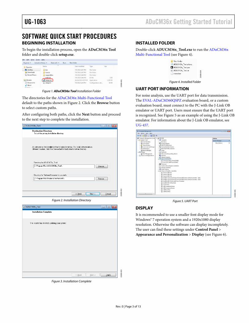
UART PORT INFORMATION For noise analysis, use the UART port for data transmission. The EVAL-ADuCM360QSPZ evaluation board, or a custom evaluation board, must connect to the PC with the J-Link OB emulator or UART port. Users must ensure that the UART port is recognized. See Figure 5 as an example of using the J-Link OB emulator. For information about the J-Link OB emulator, see UG-457.
Figure 5. UART Port
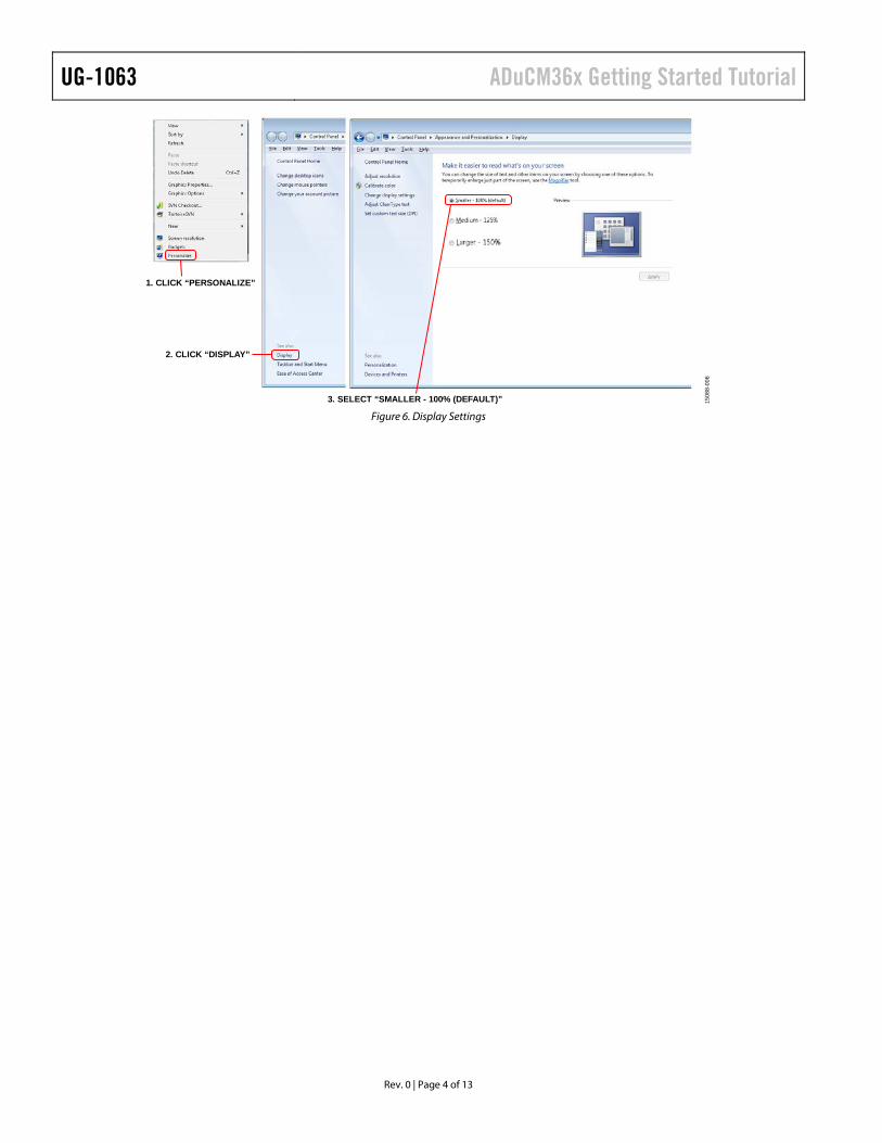
DISPLAY It is recommended to use a smaller font display mode for Windows® 7 operation system and a 1920x1080 display resolution. Otherwise the software can display incompletely. The user can find these settings under Control Panel > Appearance and Personalization > Display (see Figure 6).
1508
8-00
115
088-
002
1508
8-00
3
1508
8-00
4
1508
8-00
5
UG-1063 ADuCM36x Getting Started Tutorial
Rev. 0 | Page 4 of 13
Figure 6. Display Settings
1. CLICK “PERSONALIZE”
2. CLICK “DISPLAY”
3. SELECT “SMALLER - 100% (DEFAULT)” 1508
8-00
6
UG-1063 ADuCM36x Getting Started Tutorial
Rev. 0 | Page 5 of 13
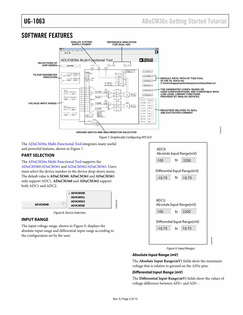
SOFTWARE FEATURES
Figure 7. Graphically Configuring AFE GUI
The ADuCM36x Multi-Functional Tool integrates many useful and powerful features, shown in Figure 7.
PART SELECTION The ADuCM36x Multi-Functional Tool supports the ADuCM360/ADuCM361 and ADuCM362/ADuCM363. Users must select the device number in the device drop-down menu. The default value is ADuCM360. ADuCM361 and ADuCM363 only support ADC1. ADuCM360 and ADuCM362 support both ADC1 and ADC2.
Figure 8. Device Selection
INPUT RANGE The input voltage range, shown in Figure 9, displays the absolute input range and differential input range according to the configuration set by the user.
Figure 9. Input Ranges
Absolute Input Range (mV)
The Absolute Input Range(mV) fields show the maximum voltage that is relative to ground on the AINx pins.
Differential Input Range (mV)
The Differential Input Range(mV) fields show the values of voltage difference between AIN+ and AIN−.
ANALOG SYSTEMSUPPLY POWER
REFERENCE INDICATIONFOR DUAL ADC
FILTER PARAMETERINDICATION
SELECTIONS OFCHIP SERIES
VOLTAGE INPUT RANGE
GROUND SWITCH AND 20kΩ RESISTOR SELECTION
REGISTERS RELATED TO ADCsAND EXCITATION CURRENT
THE GENERATED CODES, BASED ONUSER CONFIGURATIONS, ARE COMPATIBLE WITHLOW LEVEL LIBRARY FUNCTIONSPROVIDED BY ANALOG DEVICES.
DEFAULT PATH: PATH OF THIS TOOLIN THE PC SUCH AS:C:\Users\happyday\Desktop\picture\SaveData.ini
1508
8-00
7
1508
8-00
8
1508
8-00
9
UG-1063 ADuCM36x Getting Started Tutorial
Rev. 0 | Page 6 of 13
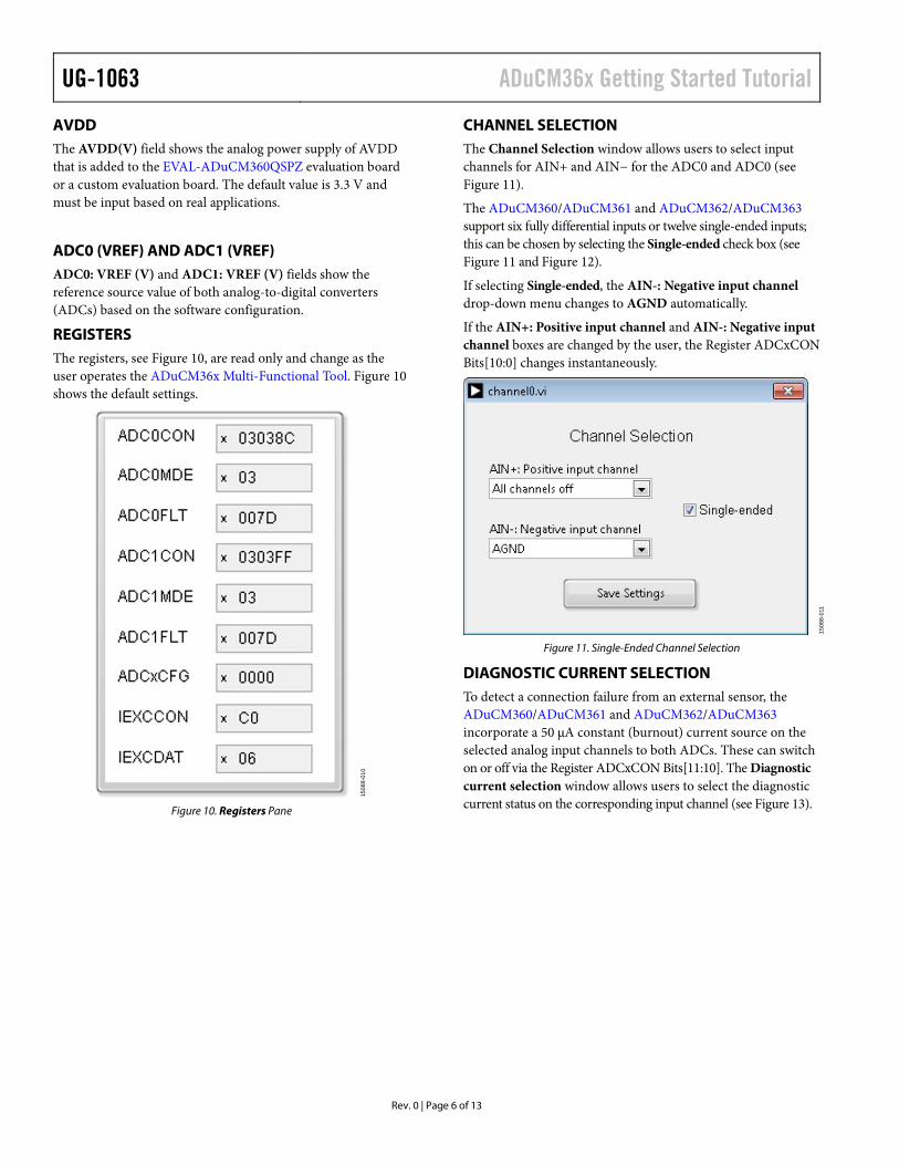
AVDD The AVDD(V) field shows the analog power supply of AVDD that is added to the EVAL-ADuCM360QSPZ evaluation board or a custom evaluation board. The default value is 3.3 V and must be input based on real applications.
ADC0 (VREF) AND ADC1 (VREF) ADC0: VREF (V) and ADC1: VREF (V) fields show the reference source value of both analog-to-digital converters (ADCs) based on the software configuration.
REGISTERS The registers, see Figure 10, are read only and change as the user operates the ADuCM36x Multi-Functional Tool. Figure 10 shows the default settings.
Figure 10. Registers Pane
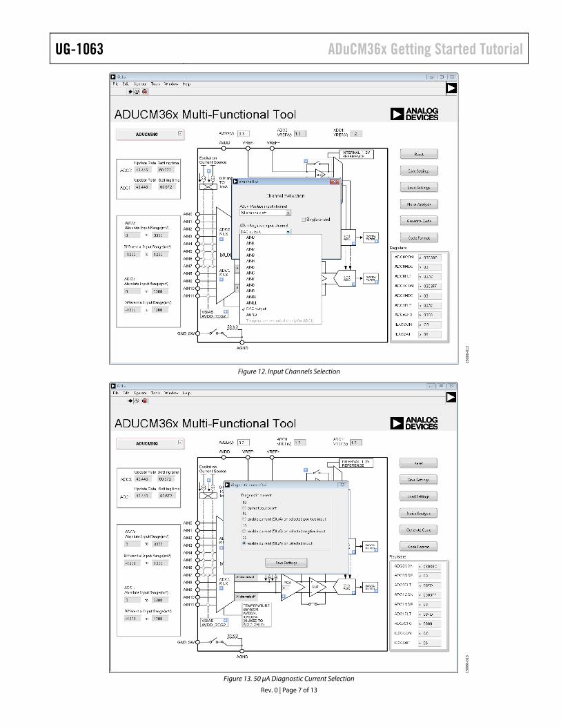
CHANNEL SELECTION The Channel Selection window allows users to select input channels for AIN+ and AIN− for the ADC0 and ADC0 (see Figure 11).
The ADuCM360/ADuCM361 and ADuCM362/ADuCM363 support six fully differential inputs or twelve single-ended inputs; this can be chosen by selecting the Single-ended check box (see Figure 11 and Figure 12).
If selecting Single-ended, the AIN-: Negative input channel drop-down menu changes to AGND automatically.
If the AIN+: Positive input channel and AIN-: Negative input channel boxes are changed by the user, the Register ADCxCON Bits[10:0] changes instantaneously.
Figure 11. Single-Ended Channel Selection
DIAGNOSTIC CURRENT SELECTION
To detect a connection failure from an external sensor, the ADuCM360/ADuCM361 and ADuCM362/ADuCM363 incorporate a 50 μA constant (burnout) current source on the selected analog input channels to both ADCs. These can switch on or off via the Register ADCxCON Bits[11:10]. The Diagnostic current selection window allows users to select the diagnostic current status on the corresponding input channel (see Figure 13).
1508
8-01
0
1508
8-01
1
UG-1063 ADuCM36x Getting Started Tutorial
Rev. 0 | Page 7 of 13
Figure 12. Input Channels Selection
Figure 13. 50 μA Diagnostic Current Selection
1508
8-01
215
088-
013
UG-1063 ADuCM36x Getting Started Tutorial
Rev. 0 | Page 8 of 13
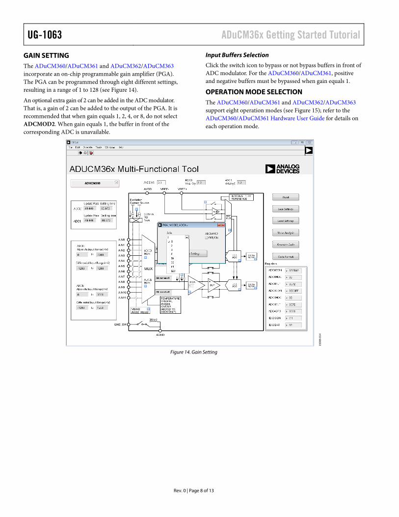
GAIN SETTING The ADuCM360/ADuCM361 and ADuCM362/ADuCM363 incorporate an on-chip programmable gain amplifier (PGA). The PGA can be programmed through eight different settings, resulting in a range of 1 to 128 (see Figure 14).
An optional extra gain of 2 can be added in the ADC modulator. That is, a gain of 2 can be added to the output of the PGA. It is recommended that when gain equals 1, 2, 4, or 8, do not select ADCMOD2. When gain equals 1, the buffer in front of the corresponding ADC is unavailable.
Input Buffers Selection
Click the switch icon to bypass or not bypass buffers in front of ADC modulator. For the ADuCM360/ADuCM361, positive and negative buffers must be bypassed when gain equals 1.
OPERATION MODE SELECTION The ADuCM360/ADuCM361 and ADuCM362/ADuCM363 support eight operation modes (see Figure 15); refer to the ADuCM360/ADuCM361 Hardware User Guide for details on each operation mode.
Figure 14. Gain Setting
1508
8-01
4

UG-1063 ADuCM36x Getting Started Tutorial
Rev. 0 | Page 9 of 13
Figure 15. Operation Mode Selection
1508
8-01
5
UG-1063 ADuCM36x Getting Started Tutorial
Rev. 0 | Page 10 of 13
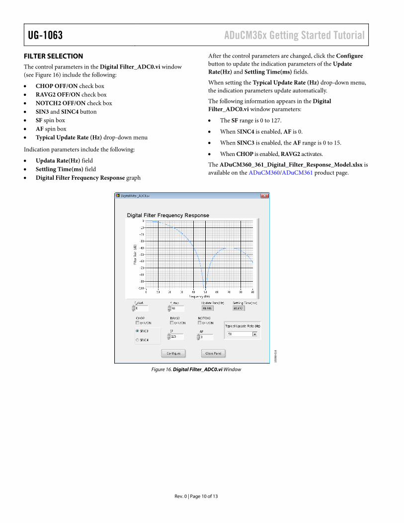
FILTER SELECTION The control parameters in the Digital Filter_ADC0.vi window (see Figure 16) include the following:
• CHOP OFF/ON check box • RAVG2 OFF/ON check box • NOTCH2 OFF/ON check box • SIN3 and SINC4 button • SF spin box • AF spin box • Typical Update Rate (Hz) drop-down menu
Indication parameters include the following:
• Updata Rate(Hz) field • Settling Time(ms) field • Digital Filter Frequency Response graph
After the control parameters are changed, click the Configure button to update the indication parameters of the Update Rate(Hz) and Settling Time(ms) fields.
When setting the Typical Update Rate (Hz) drop-down menu, the indication parameters update automatically.
The following information appears in the Digital Filter_ADC0.vi window parameters:
• The SF range is 0 to 127.
• When SINC4 is enabled, AF is 0.
• When SINC3 is enabled, the AF range is 0 to 15.
• When CHOP is enabled, RAVG2 activates.
The ADuCM360_361_Digital_Filter_Response_Model.xlsx is available on the ADuCM360/ADuCM361 product page.
Figure 16. Digital Filter_ADC0.vi Window
1508
8-01
6
UG-1063 ADuCM36x Getting Started Tutorial
Rev. 0 | Page 11 of 13
REFERENCE SELECTION Reference selection for the ADC0 and ADC1 is available in the Reference_choose.vi window (see Figure 17). EXTREF is available for ADC0 and ADC1 and EXTREF2 is only valid for ADC1. The minimum differential voltage for EXTREN and EXTREN2IN is 400 mV.
Figure 17. Reference Selection
REFERENCE BUFFER If the user chooses the external reference as an ADC reference, the ADuCM360/ADuCM361 and ADuCM362/ADuCM363 provide an option to internally buffer the external reference. The Reference Buffers window shows these four available reference buffer options (see Figure 18).
Figure 18. Reference Buffer Options
BIPOLAR/UNIPOLAR MODE SELECTION ADuCM360/ADuCM361 and ADuCM362/ADuCM363 supports two kinds of code output format: bipolar or unipolar.
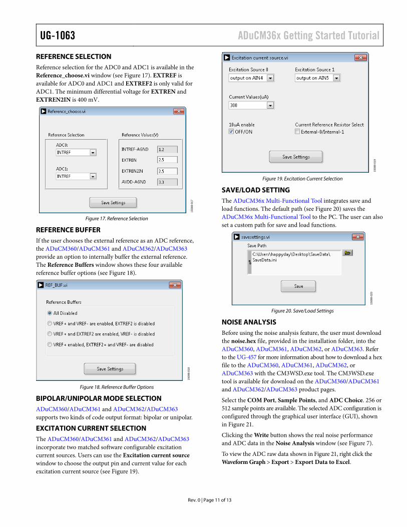
EXCITATION CURRENT SELECTION The ADuCM360/ADuCM361 and ADuCM362/ADuCM363 incorporate two matched software configurable excitation current sources. Users can use the Excitation current source window to choose the output pin and current value for each excitation current source (see Figure 19).
Figure 19. Excitation Current Selection
SAVE/LOAD SETTING The ADuCM36x Multi-Functional Tool integrates save and load functions. The default path (see Figure 20) saves the ADuCM36x Multi-Functional Tool to the PC. The user can also set a custom path for save and load functions.
Figure 20. Save/Load Settings
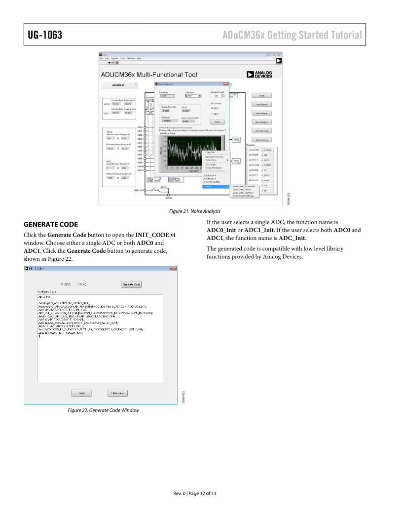
NOISE ANALYSIS Before using the noise analysis feature, the user must download the noise.hex file, provided in the installation folder, into the ADuCM360, ADuCM361, ADuCM362, or ADuCM363. Refer to the UG-457 for more information about how to download a hex file to the ADuCM360, ADuCM361, ADuCM362, or ADuCM363 with the CM3WSD.exe tool. The CM3WSD.exe tool is available for download on the ADuCM360/ADuCM361 and ADuCM362/ADuCM363 product pages.
Select the COM Port, Sample Points, and ADC Choice. 256 or 512 sample points are available. The selected ADC configuration is configured through the graphical user interface (GUI), shown in Figure 21.
Clicking the Write button shows the real noise performance and ADC data in the Noise Analysis window (see Figure 7).
To view the ADC raw data shown in Figure 21, right click the Waveform Graph > Export > Export Data to Excel.
1508
8-01
715
088-
018
1508
8-01
915
088-
020
UG-1063 ADuCM36x Getting Started Tutorial
Rev. 0 | Page 12 of 13
Figure 21. Noise Analysis
GENERATE CODE Click the Generate Code button to open the INIT_CODE.vi window. Choose either a single ADC or both ADC0 and ADC1. Click the Generate Code button to generate code, shown in Figure 22.
Figure 22. Generate Code Window
If the user selects a single ADC, the function name is ADC0_Init or ADC1_Init. If the user selects both ADC0 and ADC1, the function name is ADC_Init.
The generated code is compatible with low level library functions provided by Analog Devices.
1508
8-02
1
1508
8-02
2

UG-1063 ADuCM36x Getting Started Tutorial
Rev. 0 | Page 13 of 13
NOTES
ESD Caution ESD (electrostatic discharge) sensitive device. Charged devices and circuit boards can discharge without detection. Although this product features patented or proprietary protection circuitry, damage may occur on devices subjected to high energy ESD. Therefore, proper ESD precautions should be taken to avoid performance degradation or loss of functionality.
Legal Terms and Conditions Information furnished by Analog Devices is believed to be accurate and reliable. However, no responsibility is assumed by Analog Devices for its use, nor for any infringements of patents or other rights of third parties that may result from its use. No license is granted by implication or otherwise under any patent or patent rights of Analog Devices. Trademarks and registered trademarks are the property of their respective owners. Information contained within this document is subject to change without notice. Software or hardware provided by Analog Devices may not be disassembled, decompiled or reverse engineered. Analog Devices’ standard terms and conditions for products purchased from Analog Devices can be found at: http://www.analog.com/en/content/analog_devices_terms_and_conditions/fca.html.
©2016 Analog Devices, Inc. All rights reserved. Trademarks and registered trademarks are the property of their respective owners. UG15088-0-12/16(0)

![DC-to-DC Switching-Regulator Insights—Achieving Longer ... · By Sridhar Gurram [sridhar.gurram@analog.com] Oliver Brennan [oliver.brennan@analog.com] Tim Wilkerson [tim.wilkerson@analog.com]](https://img.dokumen.tips/doc/110x75/61219f3deb944c100772c8e6/dc-to-dc-switching-regulator-insightsaachieving-longer-by-sridhar-gurram-sridhargurram.jpg)