Embed Size (px)
Citation preview

a
ADSP-TS201 TigerSHARC® ProcessorHardware Reference
Revision 1.1, December 2004
Part Number82-000815-01
Analog Devices, Inc.One Technology WayNorwood, Mass. 02062-9106

Copyright Information© 2004 Analog Devices, Inc., ALL RIGHTS RESERVED. This document may not be reproduced in any form without prior, express written consent from Analog Devices, Inc.
Printed in the USA.
DisclaimerAnalog Devices, Inc. reserves the right to change this product without prior notice. Information furnished by Analog Devices is believed to be accurate and reliable. However, no responsibility is assumed by Analog Devices for its use; nor for any infringement of patents or other rights of third parties which may result from its use. No license is granted by implication or otherwise under the patent rights of Analog Devices, Inc.
Trademark and Service Mark NoticeThe Analog Devices logo, Blackfin, EZ-ICE, SHARC, TigerSHARC, the TigerSHARC logo, and VisualDSP++, and are registered trademarks of Analog Devices, Inc.
Static Superscalar is a trademark of Analog Devices, Inc.
All other brand and product names are trademarks or service marks of their respective owners.

ADSP-TS201 TigerSHARC Processor Hardware Reference iii
CONTENTS
CONTENTS
PREFACE
Purpose of This Manual ................................................................. xxi
Intended Audience ......................................................................... xxi
Manual Contents .......................................................................... xxii
What’s New in This Manual ......................................................... xxiv
Technical or Customer Support ..................................................... xxv
Supported Processors .................................................................... xxvi
Product Information ................................................................... xxvii
MyAnalog.com ...................................................................... xxvii
Processor Product Information ............................................... xxvii
Related Documents .............................................................. xxviii
Online Technical Documentation ........................................... xxix
Accessing Documentation From VisualDSP++ ..................... xxx
Accessing Documentation From Windows ........................... xxx
Accessing Documentation From the Web ............................ xxxi
Printed Manuals ..................................................................... xxxi

CONTENTS
iv ADSP-TS201 TigerSHARC Processor Hardware Reference
VisualDSP++ Documentation Set ...................................... xxxi
Hardware Tools Manuals .................................................. xxxii
Processor Manuals ............................................................ xxxii
Data Sheets ...................................................................... xxxii
Conventions .............................................................................. xxxiii
PROCESSOR ARCHITECTURE
Processor Core .............................................................................. 1-8
Compute Blocks ................................................................... 1-10
Arithmetic Logic Unit (ALU) ............................................ 1-12
Communications Logic Unit (CLU) .................................. 1-12
Multiply Accumulator (Multiplier) .................................... 1-12
Bit Wise Barrel Shifter (Shifter) ........................................ 1-13
Integer Arithmetic Logic Unit (IALU) ................................... 1-13
Program Sequencer ............................................................... 1-15
Processor Core Controls ........................................................ 1-17
Clock Domains ................................................................ 1-17
Operation Modes ............................................................. 1-18
User Mode ................................................................... 1-19
Supervisor Mode ........................................................... 1-20
Emulator Mode ............................................................ 1-20
Boot Modes ...................................................................... 1-22
Memory, Registers, and Buses ..................................................... 1-22
Internal Buses ....................................................................... 1-23
Internal Registers .................................................................. 1-23

ADSP-TS201 TigerSHARC Processor Hardware Reference v
CONTENTS
SOC Interface ............................................................................. 1-24
Timers ........................................................................................ 1-24
Flags ........................................................................................... 1-25
Interrupts ................................................................................... 1-26
Direct Memory Access ................................................................. 1-26
External (Address and Data) Port ................................................. 1-28
External Bus and Host Interface ............................................. 1-28
External Memory .............................................................. 1-29
Multiprocessing ................................................................ 1-30
Host Interface ................................................................... 1-31
Link Ports ................................................................................... 1-32
JTAG Port and Debug Interface .................................................. 1-32
Programming Information ........................................................... 1-33
MEMORY AND REGISTERS
Host Address Space ....................................................................... 2-4
External Memory Bank Space ........................................................ 2-4
Multiprocessor Space ..................................................................... 2-6
Internal Address Space .................................................................. 2-7
Universal (Ureg) Register Space ..................................................... 2-8
Compute Block Register Groups ............................................ 2-14
Unmapped Compute Block Registers ................................. 2-19
IALU Register Groups ........................................................... 2-22
IALU Status (J31/JSTAT and K31/KSTAT) Registers ......... 2-26
Sequencer Register Groups .................................................... 2-27

CONTENTS
vi ADSP-TS201 TigerSHARC Processor Hardware Reference
Flag Control (FLAGREG) Register ................................... 2-28
Sequencer Control (SQCTL) Register ............................... 2-29
Static Flags (SFREG) Register ........................................... 2-30
Sequencer Control Set Bits (SQCTLST) Register .............. 2-31
Sequencer Control Clear Bits (SQCTLCL) Register ........... 2-31
Sequencer Status (SQSTAT) Register ................................ 2-31
Cache Register Groups .......................................................... 2-34
Cache/Memory System Command/Status(CACMDx, CCAIRx, and CASTATx) Registers ............. 2-36
Interrupt Register Groups ..................................................... 2-41
Interrupt Vector Table Register Groups ............................. 2-41
Interrupt Control (INTCTL) Register ............................... 2-45
Interrupt Latch (ILATL/ILATH) Registers ........................ 2-46
Interrupt Pointer Mask (PMASKL/PMASKH) Registers .... 2-47
Interrupt Mask (IMASKL/IMASKH) Registers .................. 2-47
Timer Interrupt (TIMERxH/L) Registers .......................... 2-50
Timer Initial Value (TMRINxH/L) Registers ..................... 2-50
DMA Control and Status Register Group .............................. 2-51
DMA Control (DCNT) Register ....................................... 2-51
DMA Status (DSTAT) Register ......................................... 2-53
External Port DMA TCB Register Group ............................... 2-56
Link Port Transmit DMA TCB Register Group ...................... 2-57
Link Port Receive DMA TCB Register Group ........................ 2-58
AutoDMA Register Group .................................................... 2-60

ADSP-TS201 TigerSHARC Processor Hardware Reference vii
CONTENTS
DMA Index (DI), X-Dimension (DX),Y-Dimension (DY), and Pointer (DP) TCB Registers ........... 2-61
Link Port Register Groups ..................................................... 2-65
Link Receive Control (LRCTLx) Registers ......................... 2-68
Link Transmit Control (LTCTLx) Registers ....................... 2-69
Link Receive Status (LRSTATx) Registers .......................... 2-70
Link Transmit Status (LTSTATx) Registers ........................ 2-71
External Bus Interface Register Groups .................................. 2-72
System Configuration (SYSCON) Register ........................ 2-73
Bus Lock (BUSLOCK) System Control Register ................ 2-76
SDRAM Configuration (SDRCON) Register .................... 2-76
System Status (SYSTAT) Register ...................................... 2-77
Bus Master Maximum (BMAX) Register ............................ 2-80
Bus Master Maximum Current Count (BMAXC) Register .. 2-80
JTAG Test and Emulation Register Groups ............................ 2-81
Emulation Control (EMUCTL) Register ........................... 2-82
Emulation Status (EMUSTAT) Register ............................. 2-83
Silicon Version and ID Code (IDCODE) Register ............. 2-83
Debug Register Groups .......................................................... 2-84
Watchpoint Control (WPxCTL) Registers ......................... 2-86
Watchpoint Status (WPxSTAT) Registers ........................... 2-89
Watchpoint Address Pointer (WPxL/WPxH) Registers ....... 2-89
Performance Monitor Mask (PRFM) Register .................... 2-89
Performance Monitor Counter (PRFCNT) Register ........... 2-92
Cycle Counter (CCNTx) Registers .................................... 2-92

CONTENTS
viii ADSP-TS201 TigerSHARC Processor Hardware Reference
Trace Buffers and Pointer (TRCBx/TRCBPTR) Registers .. 2-93
SOC INTERFACE
SOC Interface Operations ............................................................ 3-5
SOC OFIFO Transactions ....................................................... 3-5
SOC IFIFO/OBUF Transactions ............................................. 3-7
SOC Interface Programming ......................................................... 3-8
TIMERS
Timer Operations ......................................................................... 4-2
Timer Programming ..................................................................... 4-4
Timer Expired (TMR0E) Pin and Signal Timing ........................... 4-8
FLAGS
Flag Operations ............................................................................ 5-1
Flag Programming ........................................................................ 5-3
Flag (FLAG3-0) Pin and Signal Timing ....................................... 5-10
INTERRUPTS
Interrupt Operations .................................................................... 6-5
Interrupt Service Routines ....................................................... 6-8
Handling Interrupts .......................................................... 6-13
Returning From an Interrupt ............................................ 6-14
Handling Exceptions ........................................................ 6-15
Interrupt Vector Table ........................................................... 6-17
Timer Expired Interrupts .................................................. 6-19

ADSP-TS201 TigerSHARC Processor Hardware Reference ix
CONTENTS
Link Port Service Request Interrupts .................................. 6-20
DMA Complete Interrupts ................................................ 6-20
External (IRQ3–0) Input Interrupts .................................. 6-20
Vector Interrupt ................................................................ 6-21
Bus Lock Interrupt Register ............................................... 6-21
Hardware Error Interrupt .................................................. 6-22
Software Exception Interrupts ........................................... 6-23
Emulation Exception Interrupt .......................................... 6-24
Interrupt Programming ............................................................... 6-25
Interrupt (IRQ3-0) Pin and Signal Timing .................................. 6-32
DIRECT MEMORY ACCESS
DMA Controller Features .............................................................. 7-8
Cluster Bus Transfers ............................................................... 7-8
AutoDMA Transfers .............................................................. 7-10
Link Port Transfers ................................................................ 7-10
Two-Dimensional DMA ........................................................ 7-11
Chained DMA ...................................................................... 7-11
DMA Architecture ...................................................................... 7-12
DMA Request (DMAR3-0) Pins ............................................ 7-13
Terminology .......................................................................... 7-14
Setting Up DMA Transfers .......................................................... 7-15
DMA Transfer Control Block Registers ........................................ 7-15
DMA Channel Control ......................................................... 7-16
Transfer Control Block (TCB) Registers ............................ 7-16

CONTENTS
x ADSP-TS201 TigerSHARC Processor Hardware Reference
DIx Register ................................................................. 7-18
DXx Register ................................................................ 7-18
DYx Register ................................................................ 7-19
DPx Register ................................................................ 7-19
DMA Control and Status Registers ............................................. 7-23
DMA Status Register (DSTAT/DSTATC) .............................. 7-23
DMA Control Registers ........................................................ 7-26
DCNT Register ................................................................ 7-26
DCNTST Register ........................................................... 7-27
DCNTCL Register ........................................................... 7-27
DMA Control Register Restrictions ................................... 7-27
DMA Controller Operations ....................................................... 7-31
Link Port DMA Control ....................................................... 7-31
External Port DMA Control .................................................. 7-32
AutoDMA Register Control .................................................. 7-32
DMA Transfers ..................................................................... 7-33
Internal Memory Buses ..................................................... 7-33
DMA Channels ................................................................ 7-34
DMA Memory Addressing .................................................... 7-34
DMA Channel Prioritization ................................................. 7-36
Internal Memory Bus Priority ........................................... 7-36
DMA Channel Priority ..................................................... 7-36
Rotating Priority .............................................................. 7-38
DMA Chaining ..................................................................... 7-40

ADSP-TS201 TigerSHARC Processor Hardware Reference xi
CONTENTS
Enabling and Disabling Chaining ...................................... 7-42
Generating a DMA Complete Interrupt While Chaining .... 7-42
Transfer Control Blocks and Chain Loading ...................... 7-42
Setting Up and Starting the Chain ..................................... 7-43
Chain Insertion ................................................................. 7-43
Two-Dimensional DMA ........................................................ 7-44
Two-Dimensional DMA Channel Organization ................. 7-45
Two-Dimensional DMA Operation ................................... 7-46
Examples of Two Dimensional DMA Transfers .................. 7-48
DMA Interrupts .................................................................... 7-49
Starting and Stopping DMA Sequences .................................. 7-51
Starting a DMA Sequence ................................................. 7-51
Ending a DMA Sequence .................................................. 7-52
Suspending a DMA Sequence ............................................ 7-52
Resuming a DMA Sequence .............................................. 7-52
External Port DMA ..................................................................... 7-52
Internal and External Address Generation .............................. 7-53
External Port DMA Transfer Types ........................................ 7-54
External to Internal Memory ............................................. 7-54
Internal to External Memory ............................................. 7-57
External I/O Device to External Memory (Flyby) ............... 7-60
External Memory to External I/O Device (Flyby) ............... 7-62
DMA Semaphores ............................................................. 7-63
Handshake Mode .............................................................. 7-64

CONTENTS
xii ADSP-TS201 TigerSHARC Processor Hardware Reference
Flyby Mode ...................................................................... 7-65
Link Port DMA .......................................................................... 7-66
Link Ports DMA Transfer Types ............................................ 7-66
Link Port to Internal/External Memory ............................. 7-66
Internal/External Memory to Link .................................... 7-68
Receiving Link Port to Link Port ....................................... 7-69
DMA Throughput ...................................................................... 7-71
Internal Memory DMA ......................................................... 7-71
External Memory DMA ........................................................ 7-71
DMA Operation on Boot ............................................................ 7-72
DMA Examples .......................................................................... 7-73
EXTERNAL PORT AND SDRAM INTERFACE
External Bus Features .................................................................... 8-2
Bus Interface I/O Pins .................................................................. 8-3
Processor Microarchitecture .......................................................... 8-5
SYSCON Register Programming ................................................. 8-13
Bus Width ............................................................................ 8-13
Slow Device Protocol for Bus ................................................ 8-14
Pipelined Protocol for Bus ..................................................... 8-14
Initial Value for Bus Operation .............................................. 8-15
Pipelined Protocol Interface ........................................................ 8-15
Control Signals for Pipelined Transactions ............................. 8-16
Using Basic Pipelined Transactions ........................................ 8-16
Using Burst Pipelined Transactions ........................................ 8-18

ADSP-TS201 TigerSHARC Processor Hardware Reference xiii
CONTENTS
Wait Cycles ........................................................................... 8-23
Slow Device Protocol Interface .................................................... 8-26
EPROM Interface ....................................................................... 8-32
Multiprocessing Interface ............................................................ 8-34
Bus Arbitration Protocol ........................................................ 8-38
Core Priority Access (CPA) Pin ......................................... 8-40
DMA Priority Access (DPA) Pin ........................................ 8-42
Bus Fairness (BMAX) Register ........................................... 8-44
Bus Lock (BUSLOCK) Register ......................................... 8-44
Software (Processor Core) Reset Operation ........................ 8-45
Host Processor Interface .............................................................. 8-46
Back Off (BOFF) Pin ............................................................ 8-48
SDRAM Interface ....................................................................... 8-50
SDRAM Interface I/O Pins .................................................... 8-55
SDRAM Physical Connection ................................................ 8-56
Bank Select Pins ................................................................ 8-59
Internal Address and SDRAM Physical Connection ........... 8-60
SDRAM Programming .......................................................... 8-67
Enabling SDRAM ............................................................. 8-68
Selecting the CAS Latency Value – CAS ............................ 8-69
Setting the SDRAM Buffering Option – Pipeline Depth .... 8-69
Selecting the SDRAM Page Size – Page Boundary .............. 8-70
Setting the Refresh Counter Value – Refresh Rate .............. 8-70
Selecting the Precharge to RAS Delay ................................ 8-72

CONTENTS
xiv ADSP-TS201 TigerSHARC Processor Hardware Reference
Selecting the RAS to Precharge Delay ................................ 8-72
Setting the SDRAM Power-Up Mode – Initialization Sequence ................................................ 8-73
Enabling the Extended Mode (EMR) Register ................... 8-73
Flyby Transactions ................................................................ 8-74
SDRAM Interface Throughput .............................................. 8-77
Multiprocessing Operation .................................................... 8-78
Understanding DQM Operation ........................................... 8-79
Powering Up After Reset ....................................................... 8-79
SDRAM Controller Commands ............................................ 8-80
Mode Register Set (MRS) Command ................................ 8-81
Precharge (PRE) Command .............................................. 8-83
Terminating Read/Write Cycles ..................................... 8-83
Precharging .................................................................. 8-83
Bank Active (ACT) Command .......................................... 8-84
Read Command ............................................................... 8-85
Bus Width = 64 ............................................................ 8-87
Bus Width = 32 ............................................................ 8-88
Write Command ............................................................... 8-89
Bus Width = 64 ............................................................ 8-91
Bus Width = 32 ............................................................ 8-92
Refresh (REF) Command ................................................. 8-93
Self-Refresh (SREF) Command ......................................... 8-93
Programming Example .......................................................... 8-94

ADSP-TS201 TigerSHARC Processor Hardware Reference xv
CONTENTS
LINK PORTS
Link Architecture .......................................................................... 9-2
Link I/O Pins .......................................................................... 9-4
Link Transmit and Receive Data .............................................. 9-7
Link DMA .............................................................................. 9-9
Link Block Completion ........................................................... 9-9
Link Interrupts ...................................................................... 9-10
Link Reset Initialization and Boot .......................................... 9-10
Link Alternate (Software) Initialization .................................. 9-11
Link Port Communication Protocol ............................................. 9-12
Link Port Transmission Delays .................................................... 9-17
Link Port Error Detection Mechanisms ........................................ 9-19
Link Transmitter Timeout ..................................................... 9-20
Link Receiver Timeout .......................................................... 9-20
Link Verification Error .......................................................... 9-20
Link Transmit/Receive Write Error ........................................ 9-21
Link Port Control Registers ......................................................... 9-21
Link Port Status Registers ............................................................ 9-26
JTAG PORT ANDTEST/DEBUG INTERFACE
Operating Modes ........................................................................ 10-4
Debug Resources ......................................................................... 10-5
Special Instructions ............................................................... 10-5
Watchpoints .......................................................................... 10-5

CONTENTS
xvi ADSP-TS201 TigerSHARC Processor Hardware Reference
Programming – Control and Address Pointer Registers ...... 10-5
Watchpoint Operation ...................................................... 10-6
Watchpoint Status (WPiSTAT) ......................................... 10-7
Instruction Address Trace Buffer (TBUF) .............................. 10-8
Performance Monitors ................................................................ 10-8
Cycle Counter (CCNT1–0) .................................................. 10-9
Performance Monitor Mask – PRFM ..................................... 10-9
Performance Monitor Counter ............................................ 10-10
JTAG Functionality .................................................................. 10-11
JTAG Port I/O Pins ............................................................ 10-11
JTAG Instruction Register ................................................... 10-13
Data Registers ..................................................................... 10-13
SYSTEM DESIGN
Processor Booting Methods ......................................................... 11-2
Using Boot Modes and Boot Loader Kernels .......................... 11-3
Executing a Processor Boot Operation ................................... 11-3
EPROM Boot ................................................................... 11-4
Host Boot ........................................................................ 11-5
Link Port Boot ................................................................. 11-6
No Boot ........................................................................... 11-6
Booting References ................................................................ 11-8
Hardware System Design Guidelines ........................................... 11-8
Power Supplies ...................................................................... 11-9
System Clock (SCLK) Pin ................................................... 11-10

ADSP-TS201 TigerSHARC Processor Hardware Reference xvii
CONTENTS
Considerations for SCLK Design ..................................... 11-10
Considerations for SCLK Distribution ............................ 11-11
Boundary Scan and Emulator Pins ....................................... 11-15
External Ports Pins .............................................................. 11-15
Link Ports Pins .................................................................... 11-17
Hardware Design References ................................................ 11-17
Processor Thermal Relief Methods ............................................. 11-18
Thermal Overview ............................................................... 11-19
Thermal Calculations .......................................................... 11-21
Heat Sink Basics .................................................................. 11-23
Pin Fins versus Rectangular Fins .......................................... 11-23
PCB Design for Thermal Dissipation ................................... 11-24
Thermal Simulations ........................................................... 11-25
Thermal Design Terminology .............................................. 11-26
Thermal Design References .................................................. 11-27
Other Design and Test References ............................................. 11-28
ADSP-TS201 Processor EZ-KIT Lite ................................... 11-28
ADSP-TS201S MP System Simulation and AnalysisCluster Bus Topology – Signal Integrity and PCB Design Considerations ................................................................. 11-29
IBIS Models ........................................................................ 11-29
FPGA Link Port Support ..................................................... 11-30
Recommended Reading References ............................................ 11-31
INDEX

CONTENTS
xviii ADSP-TS201 TigerSHARC Processor Hardware Reference

ADSP-TS201 TigerSHARC Processor Hardware Reference xix

xx ADSP-TS201 TigerSHARC Processor Hardware Reference

ADSP-TS201 TigerSHARC Processor Hardware Reference xxi
PREFACE
Thank you for purchasing and developing systems using TigerSHARC® processors from Analog Devices.
Purpose of This Manual The ADSP-TS201 TigerSHARC Processor Hardware Reference contains information about the DSP architecture and DSP system design for TigerSHARC processors. These are 32-bit, fixed- and floating-point digi-tal signal processors from Analog Devices for use in computing, communications, and consumer applications.
The manual provides information on how the processor core and I/O peripherals operate in the TigerSHARC processor’s architecture along with reference information about I/O peripheral features.
Intended AudienceThe primary audience for this manual is a system developer who is famil-iar with Analog Devices processors. This manual assumes that the audience has a working knowledge of the appropriate processor architec-ture and microprocessor system design. Programmers who are unfamiliar with Analog Devices processors can use this manual, but should supple-ment it with other texts (such as the appropriate programming reference manuals and data sheets) that describe your target architecture.

Manual Contents
xxii ADSP-TS201 TigerSHARC Processor Hardware Reference
Manual ContentsThe manual consists of:
• Chapter 1, Processor ArchitectureThis chapter provides an architectural overview of the TigerSHARC processor.
• Chapter 2, Memory and RegistersThis chapter defines the memory map of the ADSP-TS201 TigerSHARC processor. The memory space defines the location of each element on the TigerSHARC processor.
• Chapter 3, SOC InterfaceThis chapter discusses clocking inputs, including the three differ-ent types of operating modes in which the ADSP-TS201 TigerSHARC processor can operate and the boot modes from which the TigerSHARC processor initiates.
• Chapter 4, TimersThis chapter discusses clocking inputs, including the three differ-ent types of operating modes in which the ADSP-TS201 TigerSHARC processor can operate and the boot modes from which the TigerSHARC processor initiates.
• Chapter 5, FlagsThis chapter discusses clocking inputs, including the three differ-ent types of operating modes in which the ADSP-TS201 TigerSHARC processor can operate and the boot modes from which the TigerSHARC processor initiates.
• Chapter 6, InterruptsThis chapter discusses the various types of interrupts supported by the ADSP-TS201 TigerSHARC processor. Some of the interrupts are generated internally or externally.

ADSP-TS201 TigerSHARC Processor Hardware Reference xxiii
Preface
• Chapter 7, Direct Memory AccessThis chapter describes how the ADSP-TS201 TigerSHARC pro-cessor’s on-chip DMA controller acts as a machine for transferring data without core interruption.
• Chapter 8, External Port and SDRAM InterfaceThis chapter focuses on the external bus interface of the ADSP-TS201 TigerSHARC processor, which includes the bus arbitration logic and the external address, data and control buses, and interface to SDRAM devices.
• Chapter 9, Link PortsThis chapter describes how link ports provide point-to-point com-munications between ADSP-TS201 TigerSHARC processors in a system. The Link ports can also be used to interface with any other device that is designed to work in the same protocol.
• Chapter 10, JTAG Port and Test/Debug InterfaceThis chapter describes features of the ADSP-TS201 TigerSHARC processor that are useful for performing software debugging and services usually found in Operating System (OS) kernels.
• Chapter 11, System DesignThis chapter describes system features of the ADSP-TS201 TigerSHARC processor. These include Power, Reset, Clock, JTAG, and Booting, as well as pin descriptions and other system level information.
This hardware reference is a companion document to the ADSP-TS201 TigerSHARC Processor Programming Reference.

What’s New in This Manual
xxiv ADSP-TS201 TigerSHARC Processor Hardware Reference
What’s New in This Manual Revision 1.0 of the ADSP-TS201 TigerSHARC Processor Hardware Reference differs in a number of ways from the revision 0.2 book. In revision 1.0, the following additions and corrections have been made:
• The Processor Architecture chapter has replaced the previous Intro-duction chapter. This new chapter provides a more detailed road map to the processor architecture and processor core mode controls.
• The SOC Interface, Timers, and Flags chapters have been added. A description of the operation of all I/O peripherals as bus masters or slaves on the SOC bus has been added in all chapters.
• The Interrupts chapter has been re-ordered to provide more guid-ance on using interrupts, and a consolidated interrupt vector table has been added.
• The System Design chapter has been expanded. Many of the Engineer-to-Engineer (EE) Notes to which the revision 0.2 book referred have been added to the revision 1.0 book. The topics added include booting, system design guidelines, and thermal design guidelines.
• The index has been enhanced.
• Errata reports against the revision 0.2 book have been corrected.

ADSP-TS201 TigerSHARC Processor Hardware Reference xxv
Preface
Technical or Customer SupportYou can reach Analog Devices, Inc. Customer Support in the following ways:
• Visit the Embedded Processing and DSP products Web site athttp://www.analog.com/processors/technicalSupport
• E-mail tools questions [email protected]
• E-mail processor questions [email protected]
• Phone questions to 1-800-ANALOGD
• Contact your Analog Devices, Inc. local sales office or authorized distributor
• Send questions by mail to:
Analog Devices, Inc.
One Technology Way
P.O. Box 9106
Norwood, MA 02062-9106
USA

Supported Processors
xxvi ADSP-TS201 TigerSHARC Processor Hardware Reference
Supported ProcessorsThe following is the list of Analog Devices, Inc. processors supported in VisualDSP++®.
TigerSHARC (ADSP-TSxxx) Processors
The name “TigerSHARC” refers to a family of floating-point and fixed-point [8-bit, 16-bit, and 32-bit] processors. VisualDSP++ currently supports the following TigerSHARC processors:
ADSP-TS101, ADSP-TS201, ADSP-TS202, and ADSP-TS203
SHARC® (ADSP-21xxx) Processors
The name “SHARC” refers to a family of high-performance, 32-bit,floating-point processors that can be used in speech, sound, graphics, and imaging applications. VisualDSP++ currently supports the following SHARC processors:
ADSP-21020, ADSP-21060, ADSP-21061, ADSP-21062, ADSP-21065L, ADSP-21160, ADSP-21161, ADSP-21261, ADSP-21262, ADSP-21266, ADSP-21267, ADSP-21363, ADSP-21364, and ADSP-21365
Blackfin® (ADSP-BFxxx) Processors
The name “Blackfin” refers to a family of 16-bit, embedded processors. VisualDSP++ currently supports the following Blackfin processors:
ADSP-BF531, ADSP-BF532 (formerly ADSP-21532), ADSP-BF533, ADSP-BF535 (formerly ADSP-21535), ADSP-BF561, AD6532, and AD90747

ADSP-TS201 TigerSHARC Processor Hardware Reference xxvii
Preface
Product InformationYou can obtain product information from the Analog Devices Web site, from the product CD-ROM, or from the printed publications (manuals).
Analog Devices is online at www.analog.com. Our Web site provides infor-mation about a broad range of products—analog integrated circuits, amplifiers, converters, and digital signal processors.
MyAnalog.comMyAnalog.com is a free feature of the Analog Devices Web site that allows customization of a Web page to display only the latest information on products you are interested in. You can also choose to receive weekly e-mail notifications containing updates to the Web pages that meet your interests. MyAnalog.com provides access to books, application notes, data sheets, code examples, and more.
Registration
Visit www.myanalog.com to sign up. Click Register to use MyAnalog.com. Registration takes about five minutes and serves as a means to select the information you want to receive.
If you are already a registered user, just log on. Your user name is your e-mail address.
Processor Product InformationFor information on embedded processors and DSPs, visit our Web site at www.analog.com/processors, which provides access to technical publica-tions, data sheets, application notes, product overviews, and product announcements.

Product Information
xxviii ADSP-TS201 TigerSHARC Processor Hardware Reference
You may also obtain additional information about Analog Devices and its products in any of the following ways.
• E-mail questions or requests for information to [email protected]
• Fax questions or requests for information to1-781-461-3010 (North America)089/76 903-557 (Europe)
• Access the FTP Web site atftp ftp.analog.com or ftp 137.71.23.21 ftp://ftp.analog.com
Related DocumentsThe following publications that describe the ADSP-TS201 TigerSHARC processor (and related processors) can be ordered from any Analog Devices sales office:
• ADSP-TS201S TigerSHARC Embedded Processor Data Sheet
• ADSP-TS202S TigerSHARC Embedded Processor Data Sheet
• ADSP-TS203S TigerSHARC Embedded Processor Data Sheet
• ADSP-TS201 TigerSHARC Processor Hardware Reference
• ADSP-TS201 TigerSHARC Processor Programming Reference
For information on product related development software and Analog Devices processors, see these publications:
• VisualDSP++ User's Guide for TigerSHARC Processors
• VisualDSP++ C/C++ Compiler and Library Manual for TigerSHARC Processors

ADSP-TS201 TigerSHARC Processor Hardware Reference xxix
Preface
• VisualDSP++ Assembler and Preprocessor Manual for TigerSHARC Processors
• VisualDSP++ Linker and Utilities Manual for TigerSHARC Processors
• VisualDSP++ Kernel (VDK) User's Guide
Visit the Technical Library Web site to access all processor and tools manuals and data sheets:
http://www.analog.com/processors/resources/technicalLibrary
Online Technical Documentation Online documentation comprises the VisualDSP++ Help system, software tools manuals, hardware tools manuals, processor manuals, the Dinkum Abridged C++ library, and Flexible License Manager (FlexLM) network license manager software documentation. You can easily search across the entire VisualDSP++ documentation set for any topic of interest. For easy printing, supplementary .PDF files of most manuals are also provided.
Each documentation file type is described as follows.
File Description
.CHM Help system files and manuals in Help format
.HTM or
.HTMLDinkum Abridged C++ library and FlexLM network license manager software doc-umentation. Viewing and printing the .HTML files requires a browser, such as Internet Explorer 4.0 (or higher).
.PDF VisualDSP++ and processor manuals in Portable Documentation Format (PDF). Viewing and printing the .PDF files requires a PDF reader, such as Adobe Acrobat Reader (4.0 or higher).

Product Information
xxx ADSP-TS201 TigerSHARC Processor Hardware Reference
If documentation is not installed on your system as part of the software installation, you can add it from the VisualDSP++ CD-ROM at any time by running the Tools installation. Access the online documentation from the VisualDSP++ environment, Windows® Explorer, or the Analog Devices Web site.
Accessing Documentation From VisualDSP++
From the VisualDSP++ environment:
• Access VisualDSP++ online Help from the Help menu’s Contents, Search, and Index commands.
• Open online Help from context-sensitive user interface items (tool-bar buttons, menu commands, and windows).
Accessing Documentation From Windows
In addition to any shortcuts you may have constructed, there are many ways to open VisualDSP++ online Help or the supplementary documenta-tion from Windows.
Help system files (.CHM) are located in the Help folder, and .PDF files are located in the Docs folder of your VisualDSP++ installation CD-ROM. The Docs folder also contains the Dinkum Abridged C++ library and the FlexLM network license manager software documentation.
Using Windows Explorer
• Double-click the vdsp-help.chm file, which is the master Help sys-tem, to access all the other .CHM files.
• Double-click any file that is part of the VisualDSP++ documenta-tion set.

ADSP-TS201 TigerSHARC Processor Hardware Reference xxxi
Preface
Using the Windows Start Button
• Access VisualDSP++ online Help by clicking the Start button and choosing Programs, Analog Devices, VisualDSP++, and VisualDSP++ Documentation.
• Access the .PDF files by clicking the Start button and choosing Programs, Analog Devices, VisualDSP++, Documentation for Printing, and the name of the book.
Accessing Documentation From the Web
Download manuals at the following Web site: http://www.analog.com/processors/resources/technicalLibrary/
manuals
Select a processor family and book title. Download archive (.ZIP) files, one for each manual. Use any archive management software, such as WinZip, to decompress downloaded files.
Printed ManualsFor general questions regarding literature ordering, call the Literature Center at 1-800-ANALOGD (1-800-262-5643) and follow the prompts.
VisualDSP++ Documentation Set
To purchase VisualDSP++ manuals, call 1-603-883-2430. The manuals may be purchased only as a kit.
If you do not have an account with Analog Devices, you are referred to Analog Devices distributors. For information on our distributors, log onto http://www.analog.com/salesdir/continent.asp.

Product Information
xxxii ADSP-TS201 TigerSHARC Processor Hardware Reference
Hardware Tools Manuals
To purchase EZ-KIT Lite™ and In-Circuit Emulator (ICE) manuals, call 1-603-883-2430. The manuals may be ordered by title or by product number located on the back cover of each manual.
Processor Manuals
Hardware reference and instruction set reference manuals may be ordered through the Literature Center at 1-800-ANALOGD (1-800-262-5643), or downloaded from the Analog Devices Web site. Manuals may be ordered by title or by product number located on the back cover of each manual.
Data Sheets
All data sheets (preliminary and production) may be downloaded from the Analog Devices Web site. Only production (final) data sheets (Rev. 0, A, B, C, and so on) can be obtained from the Literature Center at 1-800-ANALOGD (1-800-262-5643); they also can be downloaded from the Web site.
To have a data sheet faxed to you, call the Analog Devices Faxback System at 1-800-446-6212. Follow the prompts and a list of data sheet code numbers will be faxed to you. If the data sheet you want is not listed, check for it on the Web site.
ADSP-TS201 TigerSHARC Processor Hardware Reference xxxiii
Preface
ConventionsText conventions used in this manual are identified and described as follows.
Additional conventions, which apply only to specific chapters, may appear throughout this document.
Example Description
Close command (File menu)
Titles in reference sections indicate the location of an item within the VisualDSP++ environment’s menu system (for example, the Close command appears on the File menu).
this | that Alternative items in syntax descriptions appear within curly brackets and separated by vertical bars; read the example as this or that. One or the other is required.
[this | that] Optional items in syntax descriptions appear within brackets and sepa-rated by vertical bars; read the example as an optional this or that.
[this,…] Optional item lists in syntax descriptions appear within brackets delimited by commas and terminated with an ellipse; read the example as an optional comma-separated list of this.
.SECTION Commands, directives, keywords, and feature names are in text with letter gothic font.
filename Non-keyword placeholders appear in text with italic style format.
Note: For correct operation, ...A Note: provides supplementary information on a related topic. In the online version of this book, the word Note appears instead of this symbol.
Caution: Incorrect device operation may result if ...Caution: Device damage may result if ... A Caution: identifies conditions or inappropriate usage of the product that could lead to undesirable results or product damage. In the online version of this book, the word Caution appears instead of this symbol.
Warning: Injury to device users may result if ... A Warning: identifies conditions or inappropriate usage of the product that could lead to conditions that are potentially hazardous for devices users. In the online version of this book, the word Warning appears instead of this symbol.

Conventions
xxxiv ADSP-TS201 TigerSHARC Processor Hardware Reference

ADSP-TS201 TigerSHARC Processor Hardware Reference 1-1
1 PROCESSOR ARCHITECTURE
The ADSP-TS201 TigerSHARC Processor Hardware Reference describes the ADSP-TS201 TigerSHARC processor architecture and hardware system support features. These descriptions provide the information required for designing and configuring TigerSHARC processor systems.
As shown in Figure 1-1 and Figure 1-2, the processor architecture consists of two divisions: the processor core (where instructions execute) and the I/O peripherals (where data is stored and off-chip I/O is processed).
This chapter provides a high level description of the processor core and peripherals architecture. More detailed descriptions appear in related chapters.This chapter introduces the following section on processor architecture:
• “Processor Core” on page 1-8
• “Memory, Registers, and Buses” on page 1-22
• “SOC Interface” on page 1-24
• “Timers” on page 1-24
• “Flags” on page 1-25
• “Interrupts” on page 1-26
• “Direct Memory Access” on page 1-26
• “External (Address and Data) Port” on page 1-28

1-2 ADSP-TS201 TigerSHARC Processor Hardware Reference
Figure 1-1. ADSP-TS201 TigerSHARC Processor Core Diagram
J-BUS DATA
IAB
PC
BTB
ADDRFETCH
COMPUTATIONAL BLOCKS
J-BUS ADDR
K-BUS DATA
K-BUS ADDR
I-BUS DATA
I-BUS ADDR
32 32
32X32 32X32
XREGISTER
FILE32x32
MU
LT
IPL
IER
ALU
SH
IFTE
R
CL
U
DAB128
128
YREGISTER
FILE32x32
MU
LT
IPL
IER
AL
U
SH
IFT
ER
CL
U
DAB128
128
32
128
32
128
32
128
DATA ADDRESS GENERATION
IAB
PC
BTB
ADDRFETCH
PROGRAMSEQUENCER
COMPUTATIONAL BLOCKS
INTEGERK-IALU
INTEGERJ-IALU
32 32
32X32 32X32
XREGISTER
FILE32x32
MU
LT
IPL
IER
ALU
SH
IFTE
R
CL
U
DAB128
128
YREGISTER
FILE32x32
MU
LT
IPL
IER
AL
U
SH
IFT
ER
CL
U
DAB128
128
32
128
32
128
32
128

ADSP-TS201 TigerSHARC Processor Hardware Reference 1-3
Processor Architecture
Figure 1-2. ADSP-TS201 TigerSHARC Processor Peripherals Diagram
T
L0
8484848484848484
IN
OUT
HOST
MULTIPROC
C-BUSARB
DATA64
LINK PORTS
JTAG PORT
EXTERNALPORT
ADDR32
6
SOC BUS
DMA
JTAG
SDRAMCTRL
EXT DMAREQ
S-BUS DATA
S-BUS ADDR
INTERNAL MEMORY BLOCKS
A D
24M BITS INTERNAL MEMORY
4xCROSSBAR CONNECT
(BUFFER/CACHE)
A D A D A D
SO
CIN
TE
RF
AC
E
L1IN
OUT
L2IN
OUT
L3IN
OUT
CTRL8
CTRL10
32
128
32
128
32
128
21
128
4
J-BUS DATA
J-BUS ADDR
K-BUS DATA
K-BUS ADDR
I-BUS DATA
I-BUS ADDR

1-4 ADSP-TS201 TigerSHARC Processor Hardware Reference
• “Link Ports” on page 1-32
• “JTAG Port and Debug Interface” on page 1-32
• “Programming Information” on page 1-33
The ADSP-TS201 processor is a 128-bit, high performance TigerSHARC processor. The ADSP-TS201 processor sets a new standard of perfor-mance for digital signal processors, combining multiple computation units for floating-point and fixed-point processing as well as very wide word widths. The ADSP-TS201 processor maintains a ‘system-on-chip’ scalable computing design philosophy, including 24M bit of on-chip DRAM, six 4K word caches (one per memory block), integrated I/O peripherals, a host processor interface, DMA controllers, LVDS link ports, and shared bus connectivity for glueless multiprocessing.
In addition to providing unprecedented performance in DSP applications in raw MFLOPS and MIPS, the ADSP-TS201 processor boosts perfor-mance measures such as MFLOPS/Watt and MFLOPS/square inch in multiprocessing applications.
As shown in Figure 1-1 and Figure 1-2, the processor has the following architectural features:
• Dual computation blocks: X and Y – each consisting of a multi-plier, ALU, CLU, shifter, and a 32-word register file
• Dual integer ALUs: J and K – each containing a 32-bit IALU and 32-word register file
• Program sequencer – Controls the program flow and contains an instruction alignment buffer (IAB) and a branch target buffer (BTB)
• Three 128-bit buses providing high bandwidth connectivity between internal memory and the rest of the processor core (com-pute blocks, IALUs, program sequencer, and SOC interface)

ADSP-TS201 TigerSHARC Processor Hardware Reference 1-5
Processor Architecture
• A 128-bit bus providing high bandwidth connectivity between internal memory and external I/O peripherals (DMA, external port, and link ports)
• External port interface including the host interface, SDRAM con-troller, static pipelined interface, four DMA channels, four LVDS link ports (each with two DMA channels), and multiprocessing support
• 24M bits of internal memory organized as six 4M bit blocks—each block containing 128K words x 32 bits; each block connects to the crossbar through its own buffers and a 128K bit, 4-way set associa-tive cache
• Debug features
• JTAG Test Access Port
Figure 1-3 illustrates a typical single processor system. A multiprocessor system is illustrated in Figure 1-4 and is discussed later in “Multiprocess-ing” on page 1-30.
The TigerSHARC processor includes several features that simplify system development. The features lie in three key areas:
• Support of IEEE floating-point formats
• IEEE Standard 1149.1 Joint Test Action Group (JTAG) serial scan path and on-chip emulation features
• Architectural features supporting high level languages and operat-ing systems

1-6 ADSP-TS201 TigerSHARC Processor Hardware Reference
The features of the TigerSHARC processor architecture that directly sup-port high level language compilers and operating systems include:
• Simple, orthogonal instruction allowing the compiler to efficiently use the multi-instruction slots
• General-purpose data and IALU register files
• 32-bit (IEEE Standard 754/854) and 40-bit floating-point and 8-, 16-, 32-, and 64-bit fixed-point native data types
Figure 1-3. Single Processor Configuration
BOFF
CONTROLIMP1–0
DMAR3–0
HBGHBR
DMA DEVICE(OPTIONAL)
DATA
MSH
FLAG3–0
ID2–0
IOEN
RAS
CAS
LDQMHDQM
SDWESDCKE
SDA10
IRQ3–0
SCLKSCLKRAT2–0
SCLK_VREF
VREF
TMR0EBM
MSSD3–0
BUSLOCK
SDRAMMEMORY
(OPTIONAL)
CS
RASCAS
DQM
WECKE
A10
ADDR
DATA
CLK
POR_IN
JTAG
ADSP-TS201S
BMSCLOCK
LINKDEVICES(4 MAX)
(OPTIONAL)
BOOTEPROM
(OPTIONAL)
ADDR
MEMORY(OPTIONAL)
OE
DATA
ADDR
DATA
HOSTPROCESSORINTERFACE(OPTIONAL)
ACK
BR7–0
CPA
MS1–0
DATA63–0
DATA
ADDR
CSACK
WE
ADDR31–0
DA
TA
CO
NT
RO
L
AD
DR
ES
S
BRSTREFERENCE
RD
WRH/WRL
DPA
DS2–0
CS
LxCLKINP/N
LxACKO
LxDATI3–0P/N
LxBCMPI
LxBCMPO
LxDATO3–0P/NLxCLKOUTP/N
LxACKI
IORDIOWR
RST_OUT
RST_IN
REFERENCE

ADSP-TS201 TigerSHARC Processor Hardware Reference 1-7
Processor Architecture
• Large address space
• Immediate address modify fields
• Easily supported relocatable code and data
• Fast save and restore of processor registers onto internal memory stacks
Figure 1-4. Multiprocessing Cluster Configuration
TigerSHARCTigerSHARCMEMORY BRIDGE
DEV DEV
DEVDEV
MSSD3–0
MS0
MSH
MS1
LVDS LINKS
LVDS LINKS
SDRAM TigerSHARC HOST IFTigerSHARC

Processor Core
1-8 ADSP-TS201 TigerSHARC Processor Hardware Reference
Processor CoreThe processor core is the part of the processor that executes instructions. The following discussion provides a some details on the processor core architecture. For more information on the processor core, see related chapters in the ADSP-TS201 TigerSHARC Processor Programming Refer-ence. This section describes:
• “Compute Blocks” on page 1-10
• “Arithmetic Logic Unit (ALU)” on page 1-12
• “Communications Logic Unit (CLU)” on page 1-12
• “Multiply Accumulator (Multiplier)” on page 1-12
• “Bit Wise Barrel Shifter (Shifter)” on page 1-13
• “Integer Arithmetic Logic Unit (IALU)” on page 1-13
• “Program Sequencer” on page 1-15
• “Processor Core Controls” on page 1-17
High performance is facilitated by the ability to execute up to four 32-bit wide instructions per cycle. The TigerSHARC processor uses a variation of a Static Superscalar™ architecture to allow the programmer to specify which instructions are executed in parallel in each cycle. The instructions do not have to be aligned in memory so that program memory is not wasted.
The 24M bit internal memory is divided into six 128K word memory blocks. Each of the four internal address/data bus pairs connect to all of the six memory blocks via a crossbar interface. The six memory blocks support up to four accesses every cycle where each memory block can per-form a 128-bit access in a cycle. Each block’s cache and prefetch mechanism improve access performance of internal memory (embedded DRAM).

ADSP-TS201 TigerSHARC Processor Hardware Reference 1-9
Processor Architecture
The external port cluster bus is 64 bits wide. The high I/O bandwidth complements the high processing speeds of the core. To facilitate the high clock rate, the ADSP-TS201 processor uses a pipelined external bus with programmable pipeline depth for interprocessor communications and for Synchronous Flow-through SRAM (SSRAM) and SDRAM.
The four LVDS link ports support point-to-point high bandwidth data transfers. Each link port supports full-duplex communication.
The processor operates with a two cycle arithmetic pipeline. The branch pipeline is four to ten cycles. A branch target buffer (BTB) is implemented to reduce branch delay.
During compute intensive operations, one or both integer ALUs compute or generate addresses for fetching up to two quad operands from two memory blocks, while the program sequencer simultaneously fetches the next quad instruction from a third memory block. In parallel, the compu-tation units can operate on previously fetched operands while the sequencer prepares for a branch.
While the core processor is doing the above, the DMA channels can be replenishing the internal memories in the background with quad data from either the external port or the link ports.
The processing core of the ADSP-TS201 processor reaches exceptionally high DSP performance through using these features:
• Computation pipeline
• Dual computation units
• Execution of up to four instructions per cycle
• Access of up to eight words per cycle from memory
The two identical computation units support floating-point as well as fixed-point arithmetic. These units (compute blocks) perform up to 6 floating-point or 24 fixed-point operations per cycle.

Processor Core
1-10 ADSP-TS201 TigerSHARC Processor Hardware Reference
Each multiplier and ALU unit can execute four 16-bit fixed-point opera-tions per cycle, using Single-Instruction, Multiple-Data (SIMD) operation. This operation boosts performance of critical imaging and sig-nal processing applications that use fixed-point data.
Compute BlocksThe TigerSHARC processor core contains two computation units called compute blocks. Each compute block contains a register file and four inde-pendent computation units—an ALU, a CLU, a multiplier, and a shifter. For meeting a wide variety of processing needs, the computation units process data in several fixed- and floating-point formats.
These formats are listed here and shown in Figure 1-5:
• Fixed-point formatThese include 64-bit long word, 32-bit normal word, 32-bit com-plex (16-bit real and 16-bit imaginary), 16-bit short word, and 8-bit byte word. For short word fixed-point arithmetic, quad paral-lel operations on quad-aligned data allow fast processing of array data. Byte operations are also supported for octal-aligned data.
• Floating-point format These include 32-bit normal word and 40-bit extended word. Floating-point operations are single or extended precision. The normal word floating-point format is the standard IEEE format, and the 40-bit extended-precision format occupies a double word (64 bits) with eight additional least significant bits (LSBs) of mantissa for greater accuracy.
Each compute block has a general-purpose, multiport, 32-word data regis-ter file for transferring data between the computation units and the data buses and storing intermediate results. All of these registers can be accessed as single-, double-, or quad-aligned registers. For more informa-tion on the register file, see Chapter 2, “Compute Block Registers” in the ADSP-TS201 TigerSHARC Processor Programming Reference.

ADSP-TS201 TigerSHARC Processor Hardware Reference 1-11
Processor Architecture
Figure 1-5. Word Format Definitions1
1 The TigerSHARC processor internal data buses are 128 bits (one quad word) wide. In a quad word, the processor can move 16 byte words, 8 short words, 4 normal words, or 2 long words over the bus at the same time.
Long Word
Data
Data Bus
Data Types
(64-bit)
Normal Word(32-bit)
Short Word(16-bit)
Byte Word(8-bit)
Extended Word(40-bit)
Register(32-bit)
DataRegister(32-bit)
DataRegister(32-bit)
DataRegister(32-bit)
(128-bit)
Dual Register
64-bit
32-bit
Dual Register
32-bit
Single Register
16-
Single Register
bit16-bit
8-bit
8-bit
8-bit
8-bit
Single Register
31 031 0 31 0 31 0
8-bit
30 23
(floating-point)

Processor Core
1-12 ADSP-TS201 TigerSHARC Processor Hardware Reference
Arithmetic Logic Unit (ALU)
The ALU performs arithmetic operations on fixed-point and float-ing-point data and logical operations on fixed-point data. The source and destination of most ALU operations is the compute block register file. For more information on ALU features, see Chapter 3, “ALU” in the ADSP-TS201 TigerSHARC Processor Programming Reference
Communications Logic Unit (CLU)
On the ADSP-TS201 processor, there is a special purpose compute unit called the communications logic unit (CLU). The CLU instructions are designed to support different algorithms used for communications appli-cations. The algorithms that are supported by the CLU instructions are:
• Viterbi Decoding
• Turbo code Decoding
• Despreading for code division multiple access (CDMA) systems
• Cross correlations used for path search
For more information on CLU features, see Chapter 4, “CLU” in the ADSP-TS201 TigerSHARC Processor Programming Reference.
Multiply Accumulator (Multiplier)
The multiplier performs fixed-point or floating-point multiplication and fixed-point multiply/accumulate operations. The multiplier supports sev-eral data types in fixed- and floating-point formats. The floating-point formats are float and float-extended, as in the ALU. The source and desti-nation of most operations is the compute block register file.
The ADSP-TS201 processor’s multiplier supports complex multiply-accu-mulate operations. Complex numbers are represented by a pair of 16-bit short words within a 32-bit word. The LSBs of the input operand repre-

ADSP-TS201 TigerSHARC Processor Hardware Reference 1-13
Processor Architecture
sent the real part, and the most significant bits (MSBs) of the input operand represent the imaginary part. For more information on multiplier features, see Chapter 5, “Multiplier” in the ADSP-TS201 TigerSHARC Processor Programming Reference.
Bit Wise Barrel Shifter (Shifter)
The shifter performs logical and arithmetic shifts, bit manipulation, field deposit, and field extraction. The shifter operates on one 64-bit, one or two 32-bit, two or four 16-bit, and four or eight 8-bit fixed-point oper-ands. Shifter operations include:
• Shifts and rotates from off-scale left to off-scale right
• Bit manipulation operations, including bit set, clear, toggle and test
• Bit field manipulation operations, including field extract and deposit, using register BFOTMP (which is internal to the shifter)
• Bit FIFO operations to support bit streams with fields of varying length
• Support for ADSP-21000 DSP family compatible fixed-point/floating-point conversion operations (such as exponent extract, number of leading ones or zeros)
For more information on shifter features, see Chapter 6, “Shifter” in the ADSP-TS201 TigerSHARC Processor Programming Reference.
Integer Arithmetic Logic Unit (IALU) The IALUs can execute standard standalone ALU operations on IALU register files. The IALUs also execute register load, store, and transfer operations, providing memory addresses when data is transferred between memory and registers. The processor has dual IALUs (the J-IALU and the K-IALU) that enable simultaneous addresses for two transactions of up to

Processor Core
1-14 ADSP-TS201 TigerSHARC Processor Hardware Reference
128 bits in parallel. The IALUs allow compute operations to execute with maximum efficiency because the computation units can be devoted exclu-sively to processing data.
Each IALU has a multiport, 32-word register file. All IALU calculations are executed in a single cycle. The IALUs support pre-modify with no update and post-modify with update address generation. Circular data buffers are implemented in hardware. The IALUs support the following types of instructions:
• Regular IALU instructions
• Move Data instructions
• Load Data instructions
• Load/Store instructions with register update
• Load/Store instructions with immediate update
For indirect addressing (instructions with update), one of the registers in the register file can be modified by another register in the file or by an immediate 8- or 32-bit value, either before (pre-modify) or after (post-modify) the access. For circular buffer addressing, a length value can be associated with the first four registers to perform automatic modulo addressing for circular data buffers; the circular buffers can be located at arbitrary boundaries in memory. Circular buffers allow efficient imple-mentation of delay lines and other data structures, which are commonly used in digital filters and Fourier transformations. The ADSP-TS201 pro-cessor circular buffers automatically handle address pointer wraparounds, reducing overhead and simplifying implementation.
The IALUs also support bit reverse addressing, which is useful for the FFT algorithm. Bit reverse addressing is implemented using a reverse carry addition that is similar to regular additions, but the carry is taken from the upper bits and is driven into lower bits.

ADSP-TS201 TigerSHARC Processor Hardware Reference 1-15
Processor Architecture
The IALU provides flexibility in moving data as single, dual, or quad words. Every instruction can execute with a throughput of one per cycle. IALU instructions execute with a single cycle of latency. Normally, there are no dependency delays between IALU instructions, but if there are, four cycles of latency can occur.
For more information on IALU features, see Chapter 7, “IALU” in the ADSP-TS201 TigerSHARC Processor Programming Reference.
Program SequencerThe program sequencer supplies instruction addresses to memory and, together with the IALUs, allows compute operations to execute with max-imum efficiency. The sequencer supports efficient branching using the branch target buffer (BTB), which reduces branch delays for conditional and unconditional instructions. The two responsibilities of the sequencer are to decode fetched instructions—separating the instruction slots of the instruction line and sending each instruction to its execution unit (com-pute blocks, IALUs, or sequencer)—and to control the program flow. The sequencer’s control flow instructions divide into two types:
• Control flow instructions. These instructions are used to direct pro-gram execution by means of jumps and to execute individual instructions conditionally.
• Immediate extension instructions. These instructions are used to extend the numeric fields used in immediate operands for the sequencer and the IALU.

Processor Core
1-16 ADSP-TS201 TigerSHARC Processor Hardware Reference
Control flow instructions divide into two types:
• Direct jumps and calls based on an immediate address operand specified in the instruction encoding. For example, ‘if <cond> jump 100;’ always jumps to address 100, if the <cond> evaluates as true.
• Indirect jumps based on an address supplied by a register. The instructions used for specifying conditional execution of a line are a subcategory of indirect jumps. For example, ‘if <cond> cjmp;’ is a jump to the address pointed to by the CJMP register.
The control flow instruction must use the first instruction slot in the instruction line.
Immediate extensions are associated with IALU or sequencer (control flow) instructions. These instructions are not specified by the program-mer, but are implied by the size of the immediate data used in the instructions. The programmer must place the instruction that requires an immediate extension in the first instruction slot and leave an empty instruction slot in the line (use only three slots), so the assembler can place the immediate extension in the second instruction slot of the instruction line.
Note that only one immediate extension may be in a single instruc-tion line.
The ADSP-TS201 processor achieves its fast execution rate by means of a ten-cycle pipeline.
Two stages of the sequencer’s pipeline actually execute in the computation units. The computation units perform single cycle operations with a two-cycle computation pipeline, meaning that results are available for use two cycles after the operation is begun. Hardware causes a stall if a result is not available in a given cycle (register dependency check). Up to two com-

ADSP-TS201 TigerSHARC Processor Hardware Reference 1-17
Processor Architecture
putation instructions per compute block can be issued in each cycle, instructing the ALU, multiplier, or shifter to perform independent, simul-taneous operations.
The branch penalty in a deeply pipelined processor, such as the ADSP-TS201 processor, can be compensated for by using a branch target buffer (BTB) and branch prediction. The branch target address is stored in the BTB. When the address of a jump instruction, which is predicted by the user to be taken in most cases, is recognized (the tag address), the corresponding jump address is read from the BTB and is used as the jump address on the next cycle. Thus, the latency of a jump is reduced from five to nine wasted cycles to zero wasted cycles. If this address is not stored in the BTB, the instruction must be fetched from memory.
Other instructions also use the BTB to speed up these types of branches. These instructions are interrupt return, call return, and computed jump instructions.
For more information on the sequencer, BTB, and immediate extensions, see Chapter 8, “Program Sequencer” in the ADSP-TS201 TigerSHARC Processor Programming Reference.
Processor Core ControlsThere are few modes and controls required for ADSP-TS201 TigerSHARC processor operation because most operational features are specified as part of instruction syntax. This section describes operational modes for the processor that are not controlled as part of instruction syntax. These controls include clock domain controls, operating mode controls, and boot mode controls.
Clock Domains
The processor uses calculated ratios of the input system clock (SCLK) clock to operate as shown in Figure 1-6. The instruction execution rate is equal to the processor core clock (CCLK). A PLL from SCLK generates

Processor Core
1-18 ADSP-TS201 TigerSHARC Processor Hardware Reference
CCLK which is phase locked. The link port clocks (LxCLKOUT pins) are generated from CCLK from a software programmable divisor, and the SOC bus clock (SOCCLK) operates at 1/2 CCLK. Memory transfers to external and link port buffers operate at the SOCCLK rate. The SCLK also provides the clock input for the external bus interface and defines the AC specification reference for the external bus signals. The external bus interface runs at the SCLK frequency.
The SCLKRATx pins define the clock multiplication of SCLK to CCLK. For information on the SCLKRATx pins settings and the maximum SCLK fre-quency, see the ADSP-TS201 TigerSHARC Embedded Processor Data Sheet.
The clock domains particularly influence the performance of operations that move data between domains over the processor’s SOC bus. For more information, see “SOC Interface” on page 1-24 and “SOC Interface” on page 3-1.
Operation Modes
The TigerSHARC processor operates in one of three modes—user, supervisor, and emulator. In user and supervisor modes, all instructions are executed normally. In user mode, however, the register access is lim-ited. Regardless of the operation mode (emulation, supervisor, or user), all instructions are executed normally.
Figure 1-6. Clock Domains
SCLKRATx
SCLK
SPD BITS,LCTLx REGISTER
PLL
/2
/CR
CCLK(INSTRUCTION RATE)
SOCCLK(PERIPHERAL BUS RATE)
LxCLKOUT(LINK OUTPUT RATE)
EXTERNAL INTERFACE

ADSP-TS201 TigerSHARC Processor Hardware Reference 1-19
Processor Architecture
The current operating mode of the TigerSHARC processor affects which components of the processor are active and can be accessed. The mode also affects which exceptions are taken and how they are handled. The mode priorities from lowest priority to highest priority are: User Mode, Supervisor Mode, and Emulator Mode.
User Mode
The user mode operation is used for algorithms and control code that does not require the manipulation of system resources. Many system resources are not accessible in user mode. If the TigerSHARC processor attempts to access these resources, an exception occurs.
User mode is often used when running code out of an operating system. The operating system kernel runs in supervisor mode, but the user code is restricted to user mode.
The registers that may be accessed by core program in user mode are:
• Register groups 0x00 to 0x09 – compute block registers
• Register groups 0x0C to 0x0F – IALU registers
• Sequencer registers – CJMP, loop counter registers LC0 and LC1, and the static flag register (SFREG)
All other registers cannot be written by the core program in user mode. An attempt to write to a protected register causes an exception. These regis-ters can still be accessed by another master (DMA, external host, and others).

Processor Core
1-20 ADSP-TS201 TigerSHARC Processor Hardware Reference
Supervisor Mode
Most code that is not intended to run under an operating system should be designed to run in supervisor mode. Supervisor mode allows the pro-gram to access all processor resources. The TigerSHARC processor is in supervisor mode when one of these two conditions is true:
• The NMOD bit in SQCTL is set. For more information, see “Sequencer Control (SQCTL) Register” on page 2-29.
• An interrupt routine is executed—indicated by non-zero PMASK. For more information, see “PMASK Register” on page 6-6.)
Normally when the TigerSHARC processor is reset (via hardware or soft-ware), it goes into idle state. It exits the idle state to a running state when an interrupt is issued. The interrupt puts the TigerSHARC processor into supervisor mode.
If the NMOD bit in SQCTL is cleared, the processor enters user mode after leaving an interrupt routine (unless it is nested inside another interrupt routine).
Emulator Mode
Emulator mode is used when controlling the processor with an emulator tool via the JTAG port. The TigerSHARC processor enters emulation mode when an emulation exception is generated. An emulation exception is generated after any one of these events:
• EMUTRAP instruction
• Watchpoint when programmed to cause emulation trap
• JTAG private instruction
• TMS rising while TEME bit in EMUCTL is set
Emulation exceptions are the highest priority exceptions or interrupts.

ADSP-TS201 TigerSHARC Processor Hardware Reference 1-21
Processor Architecture
While the TigerSHARC processor is in emulator mode, the only source of instructions is the EMUIR register. The EMUIR register is loaded via the JTAG Test Access Port (TAP). When entering this mode, the external JTAG controller (Analog EZ-ICE or other customer hardware) must be enabled. For more information, see “Sequencer Control (SQCTL) Regis-ter” on page 2-29.
When the emulation features are enabled and an emulation exception is encountered, the TigerSHARC processor enters emulation mode. When the TigerSHARC processor is operating in emulator mode, the only way it can exit emulator mode is by executing a return from interrupt (RTI).
In emulator mode, the debug registers (register group 0x1B) can be accessed only by move register-to-register or immediate data load instruc-tions. These registers cannot be loaded from or stored to memory directly.
In emulation mode, the program access to the debug registers (register groups 0x1B and 0x3D) may be executed only using the instruction:
Ureg = Ureg ;
The BTB, cycle count, performance monitors, and trace buffer are inactive in emulation mode. Except for if true—RTI (np), all control flow instructions (jump, call, RDS, conditional, and so on.) and the IDLE instruction cannot be used in emulator mode. The RTI instruction can only be used without condition.
If the external reset pin is being asserted, and an external emulation excep-tion is generated, the TigerSHARC processor core exits reset internally, enters emulator mode, and waits to fetch the value of EMUIR, which is loaded from the JTAG. In this case, only the core processor operates. The external interfaces (external port, link ports, DMA, and others) are still held in reset, although their internal registers can be accessed by the instructions inserted via JTAG and EMUIR. This feature enables an EZ-ICE to initialize the TigerSHARC processor internal registers and memory while it is still in reset and start its run from a known state.

Memory, Registers, and Buses
1-22 ADSP-TS201 TigerSHARC Processor Hardware Reference
Boot Modes
The internal memory of the TigerSHARC processor can be boot loaded from an 8-bit EPROM, a host processor, or a link port using a boot mech-anism at system power up. The TigerSHARC processor can also be run (no boot) from a memory location at startup. Selection of the boot source is controlled by the BMS strap (external) pins. For more information on boot modes, see “Processor Booting Methods” on page 11-2.
Memory, Registers, and BusesThe on-chip memory consists of six blocks of 4M bits each. Each block is 128K words, thus providing high bandwidth sufficient to support both computation units, the instruction stream and external I/O, even in very intensive operations. The ADSP-TS201 processor provides access to pro-gram, two data operands, and a system access (over the SOC bus) to different memory blocks without memory or bus constraints. The mem-ory blocks can store instructions and data interchangeably.
Each memory block is organized as 128K words of 32 bits each. The accesses are pipelined to meet one clock cycle access time needed by the core, DMA, or by the external bus. Each access can be up to four words. The six memory blocks are a resource that must be shared between the compute blocks, the IALUs, the sequencer, the external port, and the link ports. In general, if during a particular cycle more than one unit in the processor attempts to access the same memory, one of the competing units is granted access, while the other is held off for further arbitration until the following cycle—see “Bus Arbitration Protocol” on page 8-38. This type of conflict only has a small impact on performance due to the very high bandwidth afforded by the internal buses.

ADSP-TS201 TigerSHARC Processor Hardware Reference 1-23
Processor Architecture
An important benefit of large on-chip memory is that by managing the movement of data on and off chip with DMA, a system designer can real-ize high levels of determinism in execution time. Predictable and deterministic execution time is a central requirement in DSP and real-time systems.
Internal BusesThe processor core has three buses (I-bus, J-bus, and K-bus), each con-nected to all of the internal memory blocks via a crossbar interface. These buses are 128 bits wide to allow up to four instructions, or four aligned data words, to be transferred in each cycle on each bus. On-chip system elements use the SOC bus and S-bus to access memory. Only one access to each memory block is allowed in each cycle, so if the application accesses a different memory segment for each purpose (instruction fetch, load/store J-IALU and K-IALU instructions and external accesses), all transactions can be executed with no stalls.
Most registers of the ADSP-TS201 processor are classified as universal registers (Ureg ). Instructions are provided for transferring data between any two Ureg registers, between a Ureg and memory, or for the immediate load of a Ureg .This includes control registers and status registers, as well as the data registers in the register files. These transfers occur with the same timing as internal memory load/store. All registers can be accessed by register-move instructions or by external master access (another ADSP-TS201 on the same cluster bus or host), but only the core registers can be accessed by load/store instructions or load-immediate instructions.
Internal RegistersMost registers of the ADSP-TS201 processor are classified as universal registers (Ureg). Instructions are provided for transferring data between any two Ureg registers, between a Ureg and memory, or for the immediate

SOC Interface
1-24 ADSP-TS201 TigerSHARC Processor Hardware Reference
load of a Ureg. This includes control registers and status registers, as well as the data registers in the register files. These transfers occur with the same timing as internal memory load/store.
SOC InterfaceA separate system on chip (SOC) bus connects the external interfaces (external port, DMA, link ports, JTAG port, and others) to the memory system via the SOC interface and S-bus. This bus has a 128-bit wide data bus and a 32-bit wide address bus. It works at half the processor core clock rate. All data transferred between internal memory or core, and external port (cluster bus, link port, and others) passes through this bus.
As shown in Figure 1-7, the SOC bus and other buses operate at the speed of the clock in their clock domain. Data that moves from one clock domain to another (for example, a DMA to or from internal memory) must pass through arbitration and synchronization at the border of each domain. If multiple masters are requesting a bus, this arbitration can become an important factor in system performance. For more informa-tion, see “Clock Domains” on page 1-17 and “SOC Interface” on page 3-1.
TimersThe TigerSHARC processor has two general-purpose 64-bit timers—Timer 0 and Timer 1. The timers are free-running counters that are loaded with an initial value and give an indication when expiring. The indication is normally an interrupt, but could also be an external pin (TMR0E) for Timer 0. For more information, see “Timers” on page 4-1.

ADSP-TS201 TigerSHARC Processor Hardware Reference 1-25
Processor Architecture
FlagsThere are four input/output flag pins. Each pin can be individually con-figured to be an input or output. When they are configured as input flag pins, they can be used either as a condition or as a value in the SQSTAT reg-
Figure 1-7. Buses, Bus Masters, and Clock Domains
S-Bus
Memory
I-Bus
K-Bus
J-Bus
Processor CoreCompute Blocks
Integer ALUsSequencer
Non-Ureg Registers
SOCInterface
LinkPorts
ExternalPort (EBIU)
JTAGPort DMA
Timer
Interrupts
SOCBus
Flags
ClusterBus
128 Bits WideOperates at SOCCLK rate
Each 128 Bits WideOperate at CCLK rate
64 Bits WideOperates atSCLK rate
Operate atLxCLKIN/OUT
rate
Extended CoreOperates atCCLK rate
Operate atSCLK rateOperates at
TCK rate
FLAGx TMR0E DMARxIRQx

Interrupts
1-26 ADSP-TS201 TigerSHARC Processor Hardware Reference
ister. (See “Flag Control (FLAGREG) Register” on page 2-28.) After powerup reset, FLAG3–0 are inputs where static 5 kΩ pull-up resistors hold them at logic high value. For more information, see “Flags” on page 5-1.
InterruptsThe ADSP-TS201 processor has four general-purpose external interrupts, IRQ3-0. The processor also has internally generated interrupts for the two timers, DMA channels, link ports, arithmetic exceptions, multiprocessor vector interrupts, and user-defined software interrupts. Interrupts can be nested through instruction commands. Interrupts have a short latency and do not abort currently executing instructions. Interrupts vector directly to a user-supplied address in the interrupt table register file, removing the overhead of a second branch. For more information, see “Interrupts” on page 6-1.
Direct Memory AccessThe TigerSHARC processor on-chip DMA controller allows zero-over-head data transfers without processor intervention. The TigerSHARC processor can simultaneously fetch instructions and access two memories for data without relying on data or instruction caches. The DMA control-ler operates independently of the processor core, supplying addresses for internal and external memory access. The DMA channels, therefore, are not part of the core processor from a programming point of view.
The processor core has four buses, each one connected to one of the inter-nal bus masters (J-IALU, K-IALU, program sequencer, and SOC interface). Each bus can connect to any memory block. These buses are 128 bits wide to allow up to four instructions, or four aligned data words, to be transferred in each cycle on each bus. On-chip system elements also use these buses to access memory. Only one access to each memory block is allowed in each cycle, so DMA or external port transfers must compete

ADSP-TS201 TigerSHARC Processor Hardware Reference 1-27
Processor Architecture
with core accesses on the same block. Because of the large bandwidth available from each memory block, not all the memory bandwidth can be used by the core units, which leaves some memory bandwidth available for use by the processor’s DMA processes or by the bus interface to serve other DSPs’ external cluster bus master transfers to the TigerSHARC pro-cessor’s memory.
Both code and data can be downloaded to the TigerSHARC processor using DMA transfers, which can occur between the following.
• TigerSHARC processor internal memory and external memory, external peripherals or a host processor
• External memory and external peripheral devices
• External memory and link ports or between two link ports
Six DMA channels (four external port DMA channels and two autoDMA channels) are available on the TigerSHARC processor for data transfers through the external port. Eight DMA channels are available for link data transfers (two per link).
Asynchronous off-chip peripherals can control any one of four DMA channels using DMA request lines (DMAR3–0). Other DMA features include flyby (for channel 0 only), interrupt generation upon completion of DMA transfers, and DMA chaining for automatically linked DMA transfers.
For more information on DMA, see “Direct Memory Access” on page 7-1.

External (Address and Data) Port
1-28 ADSP-TS201 TigerSHARC Processor Hardware Reference
External (Address and Data) PortThe TigerSHARC processor external port provides an interface to external memory, to memory-mapped I/O, to host processor, and to additional TigerSHARC processors. The external port performs external bus arbitra-tion and supplies control signals to shared, global memory, SDRAM, and I/O devices.
The external port cluster bus can be configured to be either 32 or 64 bits wide. The high I/O bandwidth complements the high processing speeds of the core. To facilitate the high clock rate, the TigerSHARC processor uses a pipelined external bus protocol with programmable pipeline depth for external memory access and host communication. For more information on the external port, see “External Port and SDRAM Interface” on page 8-1.
External Bus and Host InterfaceThe TigerSHARC processor external port (EP) provides an interface between the core processor and the 32/64-bit parallel external bus. The external port contains FIFOs that maintain the throughput of an external bus that is shared with multiple processors and peripherals—each of which may operate at speeds other than that of the core.
The most effective way to access external data in the TigerSHARC proces-sor is through the DMA. This runs in the background, allowing the core to continue processing while new data is read in or processed data is writ-ten out. Multiple DMA data streams can occur simultaneously, and the use of FIFOs helps to maintain throughput in the system.
Burst accesses are provided through the BRST pin, which allows a slave device on the bus to accept the first address and then automatically incre-ment that address as successive data words arrive.

ADSP-TS201 TigerSHARC Processor Hardware Reference 1-29
Processor Architecture
External Memory
The TigerSHARC processor external port provides the processor interface to off-chip memory and peripherals. The off-chip memory and peripherals are included in the TigerSHARC processor unified address space. The separate on-chip buses are multiplexed at the external port to create an external system bus with a single 32-bit address bus and a single 64-bit data bus. External memory and devices can be either 32 or 64 bits wide. The TigerSHARC processor automatically packs external data into either 32-, 64-, or 128-bit word widths, the latter being more efficient for reduc-ing memory access conflicts.
On-chip decoding of high order address lines (to generate memory block select signals) facilitates addressing of external memory devices. Separate control lines are also generated for simplified addressing of page mode DRAM.
The TigerSHARC processor uses the address on the external port bus to pipeline the data. This allows interfacing to synchronous DRAM and speeds up interprocessor accesses. An option allows asynchronous opera-tion for slower devices.
External data can be accessed by DMA channels or by the core. For core accesses, the read latency can be significant—eight or more cycles. The core provides I/O buffering by stalling if the data is accessed before the data is loaded in a universal register (Ureg).
Programmable memory wait states permit peripherals with different access, hold, and disable time requirements.
External shared memory resources are assigned between processors by using semaphore operations.

External (Address and Data) Port
1-30 ADSP-TS201 TigerSHARC Processor Hardware Reference
Multiprocessing
The ADSP-TS201 processor, like the ADSP-TS101 processor, is designed for multiprocessing applications. The primary multiprocessing architec-ture supported is a cluster of up to eight TigerSHARC processors that share a common bus, a global memory, and an interface to either a host processor or to other clusters. In large multiprocessing systems, this cluster can be considered an element and connected in configurations such as tor-roid, mesh, tree, crossbar, or others. The user can provide a personal interconnect method or use the on-chip communication ports.
The ADSP-TS201 processor includes the following multiprocessing capabilities:
• On-chip bus arbitration for glueless multiprocessing
• Globally accessible internal memory and registers
• Semaphore support
• Powerful, in-circuit multiprocessing emulation
The TigerSHARC processor offers features tailored to multiprocessing systems:
• The unified address space allows direct interprocessor accesses of each TigerSHARC processor internal memory and resources.
• Distributed bus arbitration logic is included on chip for glueless connection of systems containing up to eight TigerSHARC proces-sors and a host processor.
• Bus arbitration rotates, except for host requests that always hold the highest priority.
• Processor bus lock allows indivisible read-modify-write sequences for semaphores.

ADSP-TS201 TigerSHARC Processor Hardware Reference 1-31
Processor Architecture
• A vector interrupt capability is provided for interprocessor commands.
• Broadcast writes allow simultaneous transmissions of data to all TigerSHARC processors.
Host Interface
Connecting a host processor to a cluster of TigerSHARC processors is simplified by the memory-mapped nature of the interface bus and the availability of special host bus request signals.
A host that is able to access a pipelined memory interface can be easily connected to the parallel TigerSHARC processor bus. All the internal memory, Uregs, and resources within the TigerSHARC processor, such as the DMA control registers and the internal memory, are accessible to the host.
The host interface is through the TigerSHARC processor external address and data bus, with additional lines being provided for host control. The protocol is similar to the standard TigerSHARC processor pipelined bus protocol.
The host becomes bus master of the cluster by asserting the Host Bus Request (HBR) signal. Host Bus Grant (HBG) is returned by the TigerSHARC processors when the current master grants bus by asserting HBR. The host interface is synchronous, and can be delayed a number of cycles to allow slow host access. The host can also access external memory directly.
All DMA channels are accessible to the host interface, allowing code and data transfers to be accomplished with low software overhead. The host can directly read and write the internal memory of the TigerSHARC pro-cessor and can access the DMA channel setup. Vector interrupt support is provided for efficient execution of host commands and burst-mode transfers.

Link Ports
1-32 ADSP-TS201 TigerSHARC Processor Hardware Reference
Link PortsThe TigerSHARC processor has four link ports that provide four-bit receive and four-bit transmit I/O capabilities in multiprocessing systems. The link ports have the following characteristics.
• Link clock speed is selectable as either x1/4, x1/2, x2/3, or x1 of internal clock frequency.
• Link port data is packed into 128-bit words for DMA transfer to on- or off-chip memory.
• Each link port has its own buffer registers.
• Link port transfers are controlled by acknowledge handshaking.
• Link ports support full-duplex transfer and transfers to/from the external port or other links.
For more information on the link ports, see “Link Ports” on page 9-1.
JTAG Port and Debug InterfaceThe ADSP-TS201 processor supports the IEEE Standard 1149.1 Joint Test Action Group (JTAG) port for system test. This standard defines a method for serially scanning the I/O status of each component in a sys-tem. The JTAG serial port is also used by the TigerSHARC processor emulator to gain access to the processor’s on-chip emulation features.
For more information, see “JTAG Port and Test/Debug Interface” on page 10-1.

ADSP-TS201 TigerSHARC Processor Hardware Reference 1-33
Processor Architecture
Programming InformationRefer to the ADSP-TS201 TigerSHARC Processor Programming Reference for more programming information. Information available in the pro-gramming reference includes:
• Detailed chapters on each computation unit (ALU, CLU, multi-plier, and shifter), IALU, program sequencer, and embedded DRAM (internal memory) operation
• Complete reference information on all processor instructions
• Complete reference information on instruction parallelism rules
• All available reference information on other programming topics

Programming Information
1-34 ADSP-TS201 TigerSHARC Processor Hardware Reference

ADSP-TS201 TigerSHARC Processor Hardware Reference 2-1
2 MEMORY AND REGISTERS
This chapter describes the ADSP-TS201 TigerSHARC processor memory and register map. For information on using registers for computations and memory for register loads and stores, see the ADSP-TS201 TigerSHARC Processor Programming Reference. For information on using registers for configuring the TigerSHARC processor’s peripherals, use the applicable chapters in this book.
The ADSP-TS201 TigerSHARC processor has six internal memory blocks as shown in the memory map (Figure 2-1). Each memory block consists of 4M bits of memory space, and is configured as 128K words, each 32 bits in width. There are four separate internal 128-bit data buses, each can access any of the memory blocks. Memory blocks can store instructions and data interchangeably, with one access per memory block per cycle. If the programmer ensures that program and data are in different memory blocks, then data access can occur at the same time as program fetch. The I/O processor has its own internal bus, so the I/O processor does not com-pete with the core for use of an internal bus. Thus in one cycle, up to four 128-bit transfers can occur within the core (two data transfers, one pro-gram instruction transfer, and one I/O processor interface transfer).
The TigerSHARC processor’s 32-bit address bus provides an address space of four gigawords. This address space is common to a cluster of TigerSHARC processors that share the same cluster bus. This chapter defines the memory map of each TigerSHARC processor in the system

2-2 ADSP-TS201 TigerSHARC Processor Hardware Reference
Figure 2-1. ADSP-TS201 Memory Map
RESERVED
RESERVED
INTERNAL REGISTERS (UREGS)
INTERNAL MEMORY BLOCK 4
INTERNAL MEMORY BLOCK 2
INTERNAL MEMORY BLOCK 0
0x03FFFFFF
0X001E0000
0x001E03FF
0x000DFFFF
0x000C0000
0x0009FFFF
0x00080000
0x0005FFFF
0x00040000
0x0001FFFF
0x00000000
INTERNAL SPACE
PROCESSOR ID 7
PROCESSOR ID 6
PROCESSOR ID 5
PROCESSOR ID 4
PROCESSOR ID 3
PROCESSOR ID 2
PROCESSOR ID 1
PROCESSOR ID 0
BROADCAST
HOST (MSH)
BANK 1 (MS1)
BANK 0 (MS0)
MSSD BANK 0 (MSSD0)
INTERNAL MEMORY
0x50000000
0x40000000
0x38000000
0x30000000
0x2C000000
0x28000000
0x24000000
0x20000000
0x1C000000
0x18000000
0x14000000
0x10000000
0X0C000000
0x03FFFFFF
0x00000000
GLOBAL SPACE0xFFFFFFFF
MU
LTIP
RO
CE
SS
OR
ME
MO
RY
SP
AC
EE
XT
ER
NA
LM
EM
OR
YS
PA
CE
EACH IS A COPYOF INTERNAL SPACE
RESERVED
INTERNAL MEMORY BLOCK 6
INTERNAL MEMORY BLOCK 8
0x0011FFFF
0x00100000
INTERNAL MEMORY BL OCK 10
0x0015FFFF
0x00140000
RESERVED
RESERVED
RESERVED
RESERVED
RESERVED
RESERVED
SOC REGISTERS (UREGS)0X001F0000
0x001F03FF
MSSD BANK 1 (MSSD1)
MSSD BANK 2 (MSSD2)
MSSD BANK 3 (MSSD3)
0x60000000
0x70000000
0x80000000RESERVED
RESERVED
RESERVED
RESERVED
0x54000000
0x44000000
0x64000000
0x74000000

ADSP-TS201 TigerSHARC Processor Hardware Reference 2-3
Memory and Registers
and indicates where the memory space defines the location of each ele-ment. The zones in the memory space are made up of the following regions.
• External memory bank space—the region for standard addressing of off-chip memory, including SDRAM, bank 0 (MS0), bank 1 (MS1), and Host (MSH)
• External multiprocessor space—the on-chip memory of all other TigerSHARC processors connected in a multiprocessor system
• Internal address space—the region for standard internal addressing
The global memory map is shown in Figure 2-1.
In addition to the direct accesses (normal - one 32-bit word, long - two 32-bit words, and quad - four 32-bit words), several other efficient meth-ods are available. These include Broadcast Write, Merged Distribution, and Broadcast Distribution. Broadcast Write is an external write to other DSPs in a multiprocessor cluster. Merged and Broadcast Distribution are internal access methods. For additional information on memory access methods, see “IALU” in the ADSP-TS201 TigerSHARC Processor Program-ming Reference.

Host Address Space
2-4 ADSP-TS201 TigerSHARC Processor Hardware Reference
Host Address SpaceThe host address space is the space defined for the host when it is accessed as a slave. When referring to this space, the pipelined or asynchronous protocol is used according to the host bits in the SYSCON register—for additional information on the SYSCON register see Figure 2-35 on page 2-74 and Figure 2-36 on page 2-75. The backoff signal is also effec-tive on this zone—see “Back Off (BOFF) Pin” on page 8-48. The host address is two gigawords and is divided into fields, as illustrated in Table 2-1.
External Memory Bank Space This memory space corresponds to off-chip memory and memory-mapped I/O devices (SDRAM, I/O peripherals, and other standard memory devices).
Normal external accesses are split into banks. One set of banks is for SDRAM and is accessed using external memory select pins MSSD0, MSSD1, MSSD2, and MSSD3; the access is executed in SDRAM protocol. Another set of banks is identified by external memory select pins MS0 and MS1, where the access protocol is user-configurable as pipelined or slow device proto-col, and the parameters are defined by the SYSCON register value—see section “External Bus Interface Register Groups” on page 2-72.
Table 2-1. Host Address Space
Bits Name Definition
ADDR30–0 Address Address in host range
ADDR31 Host Select Determines the type of address.If ADDR31=1, the address is in host address space
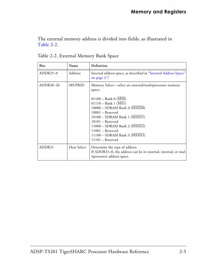
ADSP-TS201 TigerSHARC Processor Hardware Reference 2-5
Memory and Registers
The external memory address is divided into fields, as illustrated in Table 2-2.
Table 2-2. External Memory Bank Space
Bits Name Definition
ADDR25–0 Address Internal address space, as described in “Internal Address Space” on page 2-7
ADDR30–26 MS/PRID Memory Select—select an external/multiprocessor memory space:
01100 – Bank 0 (MS0)01110 – Bank 1 (MS1)10000 – SDRAM Bank 0 (MSSD0)10001 – Reserved10100 – SDRAM Bank 1 (MSSD1)10101 – Reserved11000 – SDRAM Bank 2 (MSSD2)11001 – Reserved11100 – SDRAM Bank 3 (MSSD3)11101 – Reserved
ADDR31 Host Select Determine the type of address.If ADDR31=0, the address can be in external, internal, or mul-tiprocessor address space.

Multiprocessor Space
2-6 ADSP-TS201 TigerSHARC Processor Hardware Reference
Multiprocessor SpaceThe multiprocessing space maps the internal memory space of each TigerSHARC processor in the cluster into any other TigerSHARC proces-sor. This allows one processor to easily write to and read from other processors in a multiprocessor system. Broadcast space allows write access to all TigerSHARC processors in the cluster. Each TigerSHARC processor in the cluster is identified by its ID. Valid processor ID values are 0 through 7.
The external multiprocessor address is divided into fields, as illustrated in Table 2-3.
Table 2-3. Multiprocessor Space
Bits Name Definition
ADDR25–0 Address Internal address space, as described in “Internal Address Space” on page 2-7
ADDR30–26 MS/PRID Memory Select—select an external/multiprocessor memory space:
00011 – Multiprocessor Broadcast00100 – Multiprocessor ID000101 – Multiprocessor ID100110 – Multiprocessor ID200111 – Multiprocessor ID301000 – Multiprocessor ID401001 – Multiprocessor ID501010 – Multiprocessor ID601011 – Multiprocessor ID7
ADDR31 Host Select Determine the type of address.If ADDR31=0, the address can be in external, internal, or mul-tiprocessor address space.

ADSP-TS201 TigerSHARC Processor Hardware Reference 2-7
Memory and Registers
The TigerSHARC processor’s own internal space (including Ureg regis-ters) can be accessed via the multiprocessing space (including broadcast space) for write transactions only.There are no interlocks. Because this is performed through the external bus it should only be used in special cases where data must pass through the TigerSHARC processor bus interface.
Internal Address SpaceThe internal address space corresponds to that processor’s own internal address space, Ureg registers. The internal address space is illustrated in Figure 2-1 on page 2-2.
Internal space is the space for transactions within the TigerSHARC pro-cessor and access to this memory space is not reflected on the cluster bus. Internal address space is used to access the internal memory blocks, or any of the Universal registers (Ureg). Universal registers are internal registers that are mapped to the TigerSHARC processor memory map. Most soft-ware accessible registers are Ureg registers.
Access to Ureg registers as memory locations is only available through multiprocessing space. Internal access to registers cannot be memory mapped—in load/store instructions, for example, the address cannot point to a register through the internal space. The DMA also cannot access a register directly, although there is an exception—link receive DMA chan-nels may write to other link transmit registers.

Universal (Ureg) Register Space
2-8 ADSP-TS201 TigerSHARC Processor Hardware Reference
Universal (Ureg) Register SpaceFrequently, this text refers to universal register groups and access tech-niques or restrictions that apply to particular groups. The processor’s memory-mapped, universal registers are grouped according to their rela-tionship to the processor’s architecture. For example, data registers (XR31–0, YR31–0, or XYR31–0) for the compute blocks are in one register group, while data registers (J30–0 or K30–0) for the integer ALUs (J-IALU or K-IALU) are in another register group. Each register group corresponds to a range of memory addresses because all registers in these groups are memory mapped, universal registers.
The term universal (Ureg) register indicates several important features about the register. First, the register is memory-mapped, indicating that the register can be accessed by other processors in a multiprocessor system through the register’s address. Second, the register contents can be loaded, from memory, stored to memory, or transferred to or from other Ureg reg-isters in the processor. Third, the register can be accessed as a single-, dual-, or quad-register.1
Multiprocessor accesses to another processor’s Ureg registers use the mem-ory addresses that appear in the register group tables as part of the address, but must also add the offset for a particular processor. (See the memory map in Figure 2-1 on page 2-2.) The The following code examples show multiprocessor accesses of another processor’s Ureg registers.
/* In the following multiprocessor register access example, one
processor in a multiprocessor system transfers the contents of
its XR1 register to processor P1’s XR0 register */
1 Some universal system registers (for example, sequencer register group 0x1A, DMA control/status reg-ister group 0x23, external bus interface register group 0x24, and JTAG register group 0x3D) are not accessible as dual- or quad-registers.
ADSP-TS201 TigerSHARC Processor Hardware Reference 2-9
Memory and Registers
J0 = P1_OFFSET_LOC ;;
/* P1_OFFSET_LOC is 0x1400 0000; the location of processor P1
*/
J1 = XR0_LOC ;;
/* XR0_LOC is 0x001E 0000; the location of register XR0 */
[J0 + J1] = XR1 ;;
/* transfers register XR1 data to register XR0 on proc. P1 */
For information on memory read and write instruction syntax, see the “IALU Load, Store, and Transfer (Data Addressing) Operations” section in Chapter 7, IALU, in the ADSP-TS201 TigerSHARC Processor Program-ming Reference.
A processor may not make a read access of its own Ureg registers using a multiprocessor access. Such an read access causes an illegal access exception. A processor may make a multiprocessor write access (such as a multiprocessor broadcast write) to its own Ureg registers. For more information on exceptions, see “Handling Exceptions” on page 6-15.
Load, store, or transfer Ureg register accesses within a processor use the register’s name, not its memory-mapped address. The register names appear in the register group tables. A register load access copies data from the processor’s memory and places the data into the register. A register store access copies data from the register and places the data into the pro-cessor’s memory. A register transfer (or move) access copies data from one register to another. The following code examples show single-register load, store, and transfer accesses.
/* In the following single-register load, store, and transfer
access examples, data is copied to and from single, 32-bit
registers */
XR0 = 0x76543210 ;; /* loads XR0 with immediate 32-bit data */
XR4 = [J31 + 0x43] ;; /* loads XR0 from memory */
[J0 + J4] = YR0 ;; /* stores YR0 to memory */
XR7 = SQSTAT ;; /* transfers SQSTAT contents to XR7 */

Universal (Ureg) Register Space
2-10 ADSP-TS201 TigerSHARC Processor Hardware Reference
For information on memory read and write instruction syntax, see the “IALU Load, Store, and Transfer (Data Addressing) Operations” section in Chapter 7, IALU, in the ADSP-TS201 TigerSHARC Processor Program-ming Reference.
If using legal instruction parallelism, there can be up to two load, store, or transfer accesses on an instruction line—greatly increasing performance of routines that require loading values into many reg-isters. For information on instruction parallelism, see the “Instruction Parallelism Rules” section in Chapter 1, Introduction, in the ADSP-TS201 TigerSHARC Processor Programming Reference.
Unlike the single-register accesses in the previous example that use the registers name to access a single register, dual- and quad-register accesses within a processor use a modified form of the register’s name to access mul-tiple, adjacent registers that are located on dual- or quad-word address boundaries. The modification to the register’s name indicates a range of registers, rather than a single register. For example the dual-register name XR1:0 indicates register R1 and R0 in the X compute block, and the quad-register name J31:28 indicates registers J31, J30, J29, and J28 in the J-IALU. Alignment to a dual- or quad-word address boundary refers to the register number (and address) of the lowest register in the group; dual-reg-ister boundaries end in multiples of two (for example, R1:0, R3:2, R27:26); quad-register boundaries end in multiples of four (for example, R3:0, R7:4, R31:28). The following code examples show dual- and quad-register load, store, and transfer accesses.
/* In the following dual- and quad-register load, store, and
transfer access examples data is copied to and from dual (64-bit)
and quad (128-bit) registers */
YR5:4 = L [J31 + 0x1ff0] ;; /* loads YR5:4 from memory */
XR3:0 = Q [K4 += K5] ;; /* loads XR3:0 from memory */
L [J0 + J2] = YR31:30 ;; /* stores YR31:30 to memory */
Q [K31 + K28] = YR7:4 ;; /* stores Y7:4 to memory */

ADSP-TS201 TigerSHARC Processor Hardware Reference 2-11
Memory and Registers
CACMADR0 = J1:0 ;; /* transfers J1:0 to CCAIR0:CACMD0 */
DCS0 = YR11:8 ;; /* transfers YR11:8 to DCS0 (DP, DY, DX, DI) */
For information on single-, dual-, and quad-register name instruction syn-tax, see the “Register File Registers” section in Chapter 2, Compute Block Registers, in the ADSP-TS201 TigerSHARC Processor Programming Reference.
Register groups and register quad relationships can have important influence on instruction parallelism. For information on instruc-tion parallelism, see the “Instruction Parallelism Rules” section in Chapter 1, Introduction, in the ADSP-TS201 TigerSHARC Proces-sor Programming Reference.
Normally, a register load from memory or a register store to memory access occurs between one register and a memory word of the same size—a single-register load/store of a normal (32-bit) word, a dual-register load/store of a long (64-bit) word, or a quad-register load/store of a quad (128-bit) word. When one register is loaded/stored using a memory word of the same size, the operation is called a normal read or write access. To take advantage of single-instruction, multiple-data (SIMD) processing, the processor’s bus architecture also supports types of accesses in which the contents of one memory word can be loaded into two registers (broad-cast read access) and supports types of accesses in which multiple registers can be loaded/stored with different data using one memory word (merged read or write access). For information on access types and data placement, see the “Normal, Merged, and Broadcast Memory Accesses” section in Chapter 7, IALU, in the ADSP-TS201 TigerSHARC Processor Program-ming Reference.
Note that broadcast read accesses only occur between memory and registers within a processor, while multiprocessor broadcast write accesses only occur simultaneously across all processors in a multi-processor system.

Universal (Ureg) Register Space
2-12 ADSP-TS201 TigerSHARC Processor Hardware Reference
The register space is composed of 64 register groups with up to 32 regis-ters in each group. Register groups are defined in the range 0x3F–0 (63–0), where groups 0x1F–0 are accessible by all transfer instructions (load immediate, move register, load and store), and groups 0x3F–0x20 are accessible only by move register instructions and direct accesses of other masters.
The register groups are:
• Compute block register file – groups 0x00–0x09
• IALU registers – groups 0x0C–0x0F
• Debug feature registers – groups 0x0A, 0x1B
• Program sequencer – group 0x1A
• Memory controller – groups 0x1E–0x1F
• DMA registers – groups 0x20 – 0x23
• External port control/status registers – group 0x24
• Link port registers – groups 0x25 – 0x27
• Interrupt controller – groups 0x38, 0x39, and 0x3A
• JTAG registers – group 0x3D
• AutoDMA registers – group 0x3F
• Others – Reserved. These registers must not be accessed by applica-tions since they could cause unexpected behavior by the TigerSHARC processor.
There is a direct relationship between a Ureg register’s memory-mapped address and the register group in which the register resides. (See Figure 2-2.) Because register groups have different access restrictions, it is
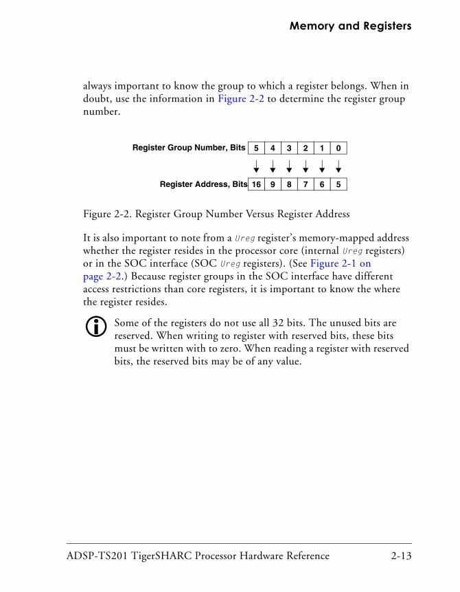
ADSP-TS201 TigerSHARC Processor Hardware Reference 2-13
Memory and Registers
always important to know the group to which a register belongs. When in doubt, use the information in Figure 2-2 to determine the register group number.
It is also important to note from a Ureg register’s memory-mapped address whether the register resides in the processor core (internal Ureg registers) or in the SOC interface (SOC Ureg registers). (See Figure 2-1 on page 2-2.) Because register groups in the SOC interface have different access restrictions than core registers, it is important to know the where the register resides.
Some of the registers do not use all 32 bits. The unused bits are reserved. When writing to register with reserved bits, these bits must be written with to zero. When reading a register with reserved bits, the reserved bits may be of any value.
Figure 2-2. Register Group Number Versus Register Address
Register Group Number, Bits
Register Address, Bits 9 8 7 6 516
4 3 2 1 05

Universal (Ureg) Register Space
2-14 ADSP-TS201 TigerSHARC Processor Hardware Reference
Compute Block Register GroupsEach compute block register file is a 32-word register. There are two such register files, one in each of the compute blocks (X and Y). The register file is aliased in several groups, some of which are applicable for data trans-fer instructions only. Some groups point to compute block X and some to block Y; those that point to both compute blocks in parallel actually point to the same register. The X and Y registers are memory mapped Universal (Ureg) registers.
The Compute Block register types of accesses are listed with their memory mapped addresses in Table 2-4, Table 2-5, Table 2-6, Table 2-7, and Table 2-8. Note that Ureg register file groups for alternative access are only for load/store instruction—DAB, circular buffer. For more informa-tion about alternate access, see the ADSP-TS201 TigerSHARC Processor Programming Reference.

ADSP-TS201 TigerSHARC Processor Hardware Reference 2-15
Memory and Registers
Table 2-4. Compute Block X Register Group
Name Address Default Name Address Default
XR0 0x1E 0000 Undefined XR16 0x1E 0010 Undefined
XR1 0x1E 0001 Undefined XR17 0x1E 0011 Undefined
XR2 0x1E 0002 Undefined XR18 0x1E 0012 Undefined
XR3 0x1E 0003 Undefined XR19 0x1E 0013 Undefined
XR4 0x1E 0004 Undefined XR20 0x1E 0014 Undefined
XR5 0x1E 0005 Undefined XR21 0x1E 0015 Undefined
XR6 0x1E 0006 Undefined XR22 0x1E 0016 Undefined
XR7 0x1E 0007 Undefined XR23 0x1E 0017 Undefined
XR8 0x1E 0008 Undefined XR24 0x1E 0018 Undefined
XR9 0x1E 0009 Undefined XR25 0x1E 0019 Undefined
XR10 0x1E 000A Undefined XR26 0x1E 001A Undefined
XR11 0x1E 000B Undefined XR27 0x1E 001B Undefined
XR12 0x1E 000C Undefined XR28 0x1E 001C Undefined
XR13 0x1E 000D Undefined XR29 0x1E 001D Undefined
XR14 0x1E 000E Undefined XR30 0x1E 001E Undefined
XR15 0x1E 000F Undefined XR31 0x1E 001F Undefined

Universal (Ureg) Register Space
2-16 ADSP-TS201 TigerSHARC Processor Hardware Reference
Table 2-5. Compute Block Y Register Group
Name Address Default Name Address Default
YR0 0x1E 0040 Undefined YR16 0x1E 0050 Undefined
YR1 0x1E 0041 Undefined YR17 0x1E 0051 Undefined
YR2 0x1E 0042 Undefined YR18 0x1E 0052 Undefined
YR3 0x1E 0043 Undefined YR19 0x1E 0053 Undefined
YR4 0x1E 0044 Undefined YR20 0x1E 0054 Undefined
YR5 0x1E 0045 Undefined YR21 0x1E 0055 Undefined
YR6 0x1E 0046 Undefined YR22 0x1E 0056 Undefined
YR7 0x1E 0047 Undefined YR23 0x1E 0057 Undefined
YR8 0x1E 0048 Undefined YR24 0x1E 0058 Undefined
YR9 0x1E 0049 Undefined YR25 0x1E 0059 Undefined
YR10 0x1E 004A Undefined YR26 0x1E 005A Undefined
YR11 0x1E 004B Undefined YR27 0x1E 005B Undefined
YR12 0x1E 004C Undefined YR28 0x1E 005C Undefined
YR13 0x1E 004D Undefined YR29 0x1E 005D Undefined
YR14 0x1E 004E Undefined YR30 0x1E 005E Undefined
YR15 0x1E 004F Undefined YR31 0x1E 005F Undefined
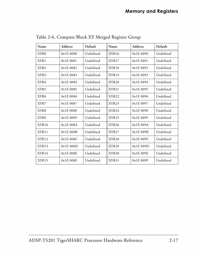
ADSP-TS201 TigerSHARC Processor Hardware Reference 2-17
Memory and Registers
Table 2-6. Compute Block XY Merged Register Group
Name Address Default Name Address Default
XYR0 0x1E 0080 Undefined XYR16 0x1E 0090 Undefined
XYR1 0x1E 0081 Undefined XYR17 0x1E 0091 Undefined
XYR2 0x1E 0082 Undefined XYR18 0x1E 0092 Undefined
XYR3 0x1E 0083 Undefined XYR19 0x1E 0093 Undefined
XYR4 0x1E 0084 Undefined XYR20 0x1E 0094 Undefined
XYR5 0x1E 0085 Undefined XYR21 0x1E 0095 Undefined
XYR6 0x1E 0086 Undefined XYR22 0x1E 0096 Undefined
XYR7 0x1E 0087 Undefined XYR23 0x1E 0097 Undefined
XYR8 0x1E 0088 Undefined XYR24 0x1E 0098 Undefined
XYR9 0x1E 0089 Undefined XYR25 0x1E 0099 Undefined
XYR10 0x1E 008A Undefined XYR26 0x1E 009A Undefined
XYR11 0x1E 008B Undefined XYR27 0x1E 009B Undefined
XYR12 0x1E 008C Undefined XYR28 0x1E 009C Undefined
XYR13 0x1E 008D Undefined XYR29 0x1E 009D Undefined
XYR14 0x1E 008E Undefined XYR30 0x1E 009E Undefined
XYR15 0x1E 008F Undefined XYR31 0x1E 009F Undefined

Universal (Ureg) Register Space
2-18 ADSP-TS201 TigerSHARC Processor Hardware Reference
Table 2-7. Compute Block YX Merged Register Group
Name Address Default Name Address Default
YXR0 0x1E 00C0 Undefined YXR16 0x1E 00D0 Undefined
YXR1 0x1E 00C1 Undefined YXR17 0x1E 00D1 Undefined
YXR2 0x1E 00C2 Undefined YXR18 0x1E 00D2 Undefined
YXR3 0x1E 00C3 Undefined YXR19 0x1E 00D3 Undefined
YXR4 0x1E 00C4 Undefined YXR20 0x1E 00D4 Undefined
YXR5 0x1E 00C5 Undefined YXR21 0x1E 00D5 Undefined
YXR6 0x1E 00C6 Undefined YXR22 0x1E 00D6 Undefined
YXR7 0x1E 00C7 Undefined YXR23 0x1E 00D7 Undefined
YXR8 0x1E 00C8 Undefined YXR24 0x1E 00D8 Undefined
YXR9 0x1E 00C9 Undefined YXR25 0x1E 00D9 Undefined
YXR10 0x1E 00CA Undefined YXR26 0x1E 00DA Undefined
YXR11 0x1E 00CB Undefined YXR27 0x1E 00DB Undefined
YXR12 0x1E 00CC Undefined YXR28 0x1E 00DC Undefined
YXR13 0x1E 00CD Undefined YXR29 0x1E 00DD Undefined
YXR14 0x1E 00CE Undefined YXR30 0x1E 00DE Undefined
YXR15 0x1E 00CF Undefined YXR31 0x1E 00DF Undefined
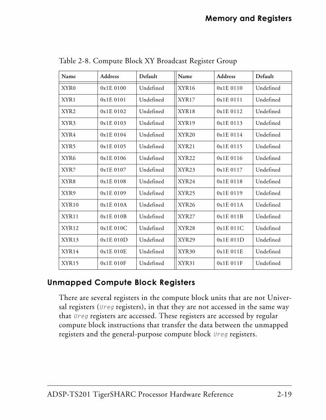
ADSP-TS201 TigerSHARC Processor Hardware Reference 2-19
Memory and Registers
Unmapped Compute Block Registers
There are several registers in the compute block units that are not Univer-sal registers (Ureg registers), in that they are not accessed in the same way that Ureg registers are accessed. These registers are accessed by regular compute block instructions that transfer the data between the unmapped registers and the general-purpose compute block Ureg registers.
Table 2-8. Compute Block XY Broadcast Register Group
Name Address Default Name Address Default
XYR0 0x1E 0100 Undefined XYR16 0x1E 0110 Undefined
XYR1 0x1E 0101 Undefined XYR17 0x1E 0111 Undefined
XYR2 0x1E 0102 Undefined XYR18 0x1E 0112 Undefined
XYR3 0x1E 0103 Undefined XYR19 0x1E 0113 Undefined
XYR4 0x1E 0104 Undefined XYR20 0x1E 0114 Undefined
XYR5 0x1E 0105 Undefined XYR21 0x1E 0115 Undefined
XYR6 0x1E 0106 Undefined XYR22 0x1E 0116 Undefined
XYR7 0x1E 0107 Undefined XYR23 0x1E 0117 Undefined
XYR8 0x1E 0108 Undefined XYR24 0x1E 0118 Undefined
XYR9 0x1E 0109 Undefined XYR25 0x1E 0119 Undefined
XYR10 0x1E 010A Undefined XYR26 0x1E 011A Undefined
XYR11 0x1E 010B Undefined XYR27 0x1E 011B Undefined
XYR12 0x1E 010C Undefined XYR28 0x1E 011C Undefined
XYR13 0x1E 010D Undefined XYR29 0x1E 011D Undefined
XYR14 0x1E 010E Undefined XYR30 0x1E 011E Undefined
XYR15 0x1E 010F Undefined XYR31 0x1E 011F Undefined

Universal (Ureg) Register Space
2-20 ADSP-TS201 TigerSHARC Processor Hardware Reference
Compute Block Status (XSTAT/YSTAT) Registers
The XSTAT and YSTAT registers are 32-bit compute block status registers that record the state of the compute block status flags. Every flag is updated when an instruction belonging to its computation unit is com-pleted. The X/YSTAT registers (reset value = 0x0000 0000) appear in Figure 2-3 and Figure 2-4. For more information on using the X/YSTAT registers, see the “Compute Block Registers” chapter in the ADSP-TS201 TigerSHARC Processor Programming Reference.
ALU Registers
The Parallel Results registers (PR0 and PR1) are two 32-bit registers used for sideways sum instructions. For more information regarding the PRx registers, see “ALU” in the ADSP-TS201 TigerSHARC Processor Program-ming Reference.
31 30 29 28 27 26 25 24 23 22 21 20 19 18 17 16
0 0 0 0 0 0 0 0 0 0 0 0 0 0 0 0 MIS—Multiplier floating-pt. invalid op., stickyMOS—Multiplier fixed-pt. overflow, stickyMVS—Multiplier floating-pt. overflow, stickyMUS—Multiplier floating-pt, underflow, stickyAIS—ALU floating-pt. invalid op., stickyAOS—ALU fixed-pt. overflow, stickyAVS—ALU floating-pt. overflow, stickyAUS—ALU floating-pt. underflow,stickyReservedIVEN—Exception enable on invalid floating-pt.OEN—Exception enable on overflow statusUEN—Exception enable on underflow statusReserved
Figure 2-3. XSTAT/YSTAT (Upper) Register Bit Descriptions

ADSP-TS201 TigerSHARC Processor Hardware Reference 2-21
Memory and Registers
Multiplier Registers
The Multiplier Results registers (MR3–0 and MR4) are used as accumulators for the different types of fixed-point Multiply-Accumulate instructions. For more information regarding the MRx registers, see “Multiplier” in the ADSP-TS201 TigerSHARC Processor Programming Reference. These regis-ters are accessed by different multiplier instructions.
Shifter Registers
The Bit FIFO Overflow register (BFOTMP) is a 64-bit register used in the PUTBITS instruction. For more information regarding the BFOTMP register, see the PUTBITS instruction in the ADSP-TS201 TigerSHARC Processor Programming Reference.
15 14 13 12 11 10 9 8 7 6 5 4 3 2 1 0
0 0 0 0 0 0 0 0 0 0 0 0 0 0 0 0
AZ—ALU zeroAN—ALU negativeAV—ALU overflowAC—ALU carryMZ—Multiplier zeroMN—Multiplier negativeMV—Multiplier overflowMU—Multiplier underflowSZ—Shifter zeroSN—Shifter negativeBF—Shifter Block floating-point flagsAI—ALU floating-point invalid operationMI—Multiplier floating-point invalid operationTROV—CLU trellis overflowTRSOV—CLU trellis overflow, sticky
Figure 2-4. XSTAT/YSTAT (Lower) Register Bit Descriptions

Universal (Ureg) Register Space
2-22 ADSP-TS201 TigerSHARC Processor Hardware Reference
Communications Logic Unit (CLU) Registers
The CLU instructions use Trellis (TR31–0) data registers, Trellis history (THR3–0) registers, and/or the Communication Control (CMCTL) register. Each register is 32 bits wide. For more information regarding these regis-ters, see the “CLU” chapter in the ADSP-TS201 TigerSHARC Processor Programming Reference.
IALU Register GroupsEach IALU has two Ureg groups. The first group is the general-purpose register file, which includes 32 normal-word registers each. The second group is the circular buffer register file which is used to specify parameters for circular buffering. The IALU register groups are listed in Table 2-9, Table 2-10, Table 2-11, and Table 2-12.
The circular buffer register files contain these registers:
• 3–0 circular buffer base registers JB3–0 and KB3–0
• 7–4 circular buffer length registers JL3–0 and KL3–0
• 31–8 Reserved

ADSP-TS201 TigerSHARC Processor Hardware Reference 2-23
Memory and Registers
Table 2-9. J-IALU Register Group
Name Address Default Name Address Default
J0 0x1E 0180 Undefined J16 0x1E 0190 Undefined
J1 0x1E 0181 Undefined J17 0x1E 0191 Undefined
J2 0x1E 0182 Undefined J18 0x1E 0192 Undefined
J3 0x1E 0183 Undefined J19 0x1E 0193 Undefined
J4 0x1E 0184 Undefined J20 0x1E 0194 Undefined
J5 0x1E 0185 Undefined J21 0x1E 0195 Undefined
J6 0x1E 0186 Undefined J22 0x1E 0196 Undefined
J7 0x1E 0187 Undefined J23 0x1E 0197 Undefined
J8 0x1E 0188 Undefined J24 0x1E 0198 Undefined
J9 0x1E 0189 Undefined J25 0x1E 0199 Undefined
J10 0x1E 018A Undefined J26 0x1E 019A Undefined
J11 0x1E 018B Undefined J27 0x1E 019B Undefined
J12 0x1E 018C Undefined J28 0x1E 019C Undefined
J13 0x1E 018D Undefined J29 0x1E 019D Undefined
J14 0x1E 018E Undefined J30 0x1E 019E Undefined
J15 0x1E 018F Undefined J31 0x1E 019F Undefined

Universal (Ureg) Register Space
2-24 ADSP-TS201 TigerSHARC Processor Hardware Reference
Table 2-10. K-IALU Register Group
Name Address Default Name Address Default
K0 0x1E 01A0 Undefined K16 0x1E 01B0 Undefined
K1 0x1E 01A1 Undefined K17 0x1E 01B1 Undefined
K2 0x1E 01A2 Undefined K18 0x1E 01B2 Undefined
K3 0x1E 01A3 Undefined K19 0x1E 01B3 Undefined
K4 0x1E 01A4 Undefined K20 0x1E 01B4 Undefined
K5 0x1E 01A5 Undefined K21 0x1E 01B5 Undefined
K6 0x1E 01A6 Undefined K22 0x1E 01B6 Undefined
K7 0x1E 01A7 Undefined K23 0x1E 01B7 Undefined
K8 0x1E 01A8 Undefined K24 0x1E 01B8 Undefined
K9 0x1E 01A9 Undefined K25 0x1E 01B9 Undefined
K10 0x1E 01AA Undefined K26 0x1E 01BA Undefined
K11 0x1E 01AB Undefined K27 0x1E 01BB Undefined
K12 0x1E 01AC Undefined K28 0x1E 01BC Undefined
K13 0x1E 01AD Undefined K29 0x1E 01BD Undefined
K14 0x1E 01AE Undefined K30 0x1E 01BE Undefined
K15 0x1E 01AF Undefined K31 0x1E 01BF Undefined

ADSP-TS201 TigerSHARC Processor Hardware Reference 2-25
Memory and Registers
Table 2-11. J-IALU Circular Buffer Register Group
Name Address Default
JB0 0x1E 01C0 Undefined
JB1 0x1E 01C1 Undefined
JB2 0x1E 01C2 Undefined
JB3 0x1E 01C3 Undefined
JL0 0x1E 01C4 Undefined
JL1 0x1E 01C5 Undefined
JL2 0x1E 01C6 Undefined
JL3 0x1E 01C7 Undefined
Reserved 0x1E 01C8–0x1E 01DF
N/A
Table 2-12. K-IALU Circular Buffer Register Group
Name Address Default
KB0 0x1E 01E0 Undefined
KB1 0x1E 01E1 Undefined
KB2 0x1E 01E2 Undefined
KB3 0x1E 01E3 Undefined
KL0 0x1E 01E4 Undefined
KL1 0x1E 01E5 Undefined
KL2 0x1E 01E6 Undefined
KL3 0x1E 01E7 Undefined
Reserved 0x1E 01E8–0x1E 01FF
N/A

Universal (Ureg) Register Space
2-26 ADSP-TS201 TigerSHARC Processor Hardware Reference
IALU Status (J31/JSTAT and K31/KSTAT) Registers
The JSTAT (for the J-IALU) and KSTAT (for the K-IALU) status registers records the state of the carry flags and is updated as a result of various IALU instructions. When being written to, the JSTAT register can be referred to as J31. When used as an operand in an IALU arithmetic, logi-cal, or function operation—J31 is treated as zero. The J31/JSTAT (K31/KSTAT ) registers (reset value = 0x0000 0000) appear in Figure 2-5. For information on using the J31/JSTAT (K31/KSTAT ) registers, see the “IALU” chapter of the ADSP-TS201 TigerSHARC Processor Programming Reference.
15 14 13 12 11 10 9 8 7 6 5 4 3 2 1 0
0 0 0 0 0 0 0 0 0 0 0 0 0 0 0 0
JZ J-IALU zeroJN J-IALU negativeJV J-IALU overflowJC J-IALU carryReserved
Figure 2-5. JSTAT/KSTAT (Lower Half) Register Bit Descriptions1
1 Bits 31–16 (not shown) are reserved (=0).

ADSP-TS201 TigerSHARC Processor Hardware Reference 2-27
Memory and Registers
Sequencer Register GroupsThis 32-bit register group is dedicated to sequencer registers, interrupt control, and status registers. See Table 2-13. All sequencer registers are accessible by single-word access only. For more information regarding the sequencer registers, see “Program Sequencer” in the ADSP-TS201 TigerSHARC Processor Programming Reference.
Table 2-13. Sequencer Register Group
Name Description Address Default
CJMP Computed jump address1 0x1E 0340 Undefined
Reserved N/A 0x1E 0341 N/A
RETI Return from interrupt address 0x1E 0342 Undefined
RETIB RETI alias, for interrupt nesting2 0x1E 0343 Undefined
RETS Return from subroutine address3 0x1E 0344 Undefined
DBGE Return from emulation address3 0x1E 0345 Undefined
Reserved N/A 0x1E 0346–0x1E 0347 N/A
LC0 Loop counter #0 0x1E 0348 Undefined
LC1 Loop counter #1 0x1E 0349 Undefined
Reserved N/A 0x1E 034A–0x1E 034F N/A
IVSW Software exception 0x1E 0350 Undefined
Reserved N/A 0x1E 0351–0x1E 0353 N/A
FLAGREG Flag control register 0x1E 0354 0x0000 0000
FLAGREGST Flag register set 0x1E 0355 Undefined
FLAGREGCL Flag register clear 0x1E 0356 Undefined
Reserved N/A 0x1E 0357 N/A
SQCTL Sequencer control register 0x1E 0358 0x0000 0004
SQCTLST Sequencer control register set bits 0x1E 0359 Undefined
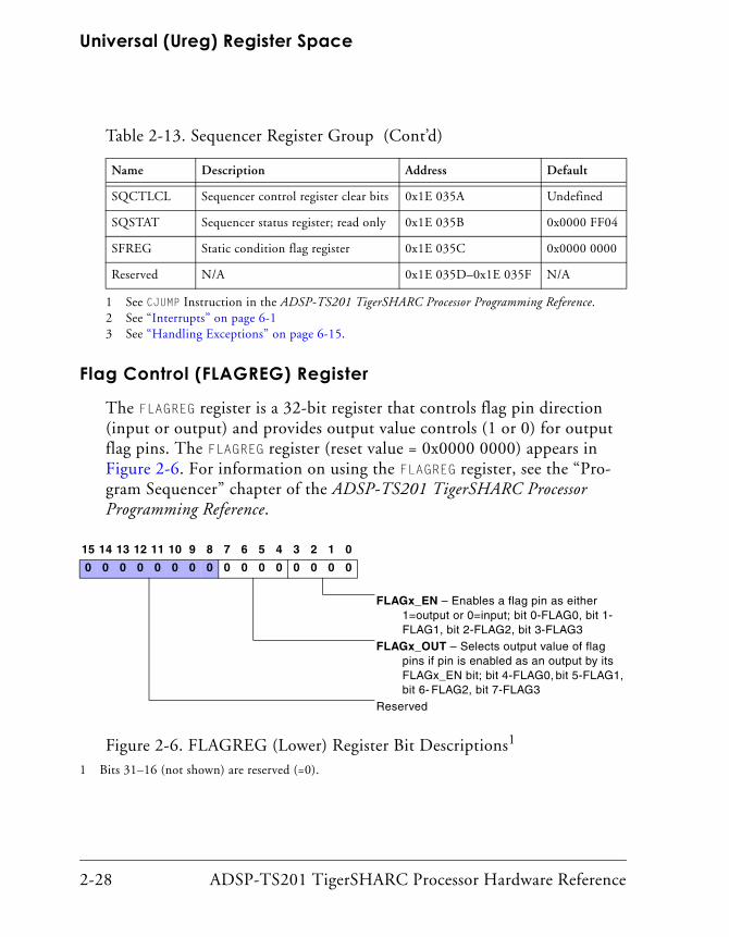
Universal (Ureg) Register Space
2-28 ADSP-TS201 TigerSHARC Processor Hardware Reference
Flag Control (FLAGREG) Register
The FLAGREG register is a 32-bit register that controls flag pin direction (input or output) and provides output value controls (1 or 0) for output flag pins. The FLAGREG register (reset value = 0x0000 0000) appears in Figure 2-6. For information on using the FLAGREG register, see the “Pro-gram Sequencer” chapter of the ADSP-TS201 TigerSHARC Processor Programming Reference.
SQCTLCL Sequencer control register clear bits 0x1E 035A Undefined
SQSTAT Sequencer status register; read only 0x1E 035B 0x0000 FF04
SFREG Static condition flag register 0x1E 035C 0x0000 0000
Reserved N/A 0x1E 035D–0x1E 035F N/A
1 See CJUMP Instruction in the ADSP-TS201 TigerSHARC Processor Programming Reference.2 See “Interrupts” on page 6-13 See “Handling Exceptions” on page 6-15.
15 14 13 12 11 10 9 8 7 6 5 4 3 2 1 0
0 0 0 0 0 0 0 0 0 0 0 0 0 0 0 0
FLAGx_EN – Enables a flag pin as either 1=output or 0=input; bit 0-FLAG0, bit 1-FLAG1, bit 2-FLAG2, bit 3-FLAG3
FLAGx_OUT – Selects output value of flag pins if pin is enabled as an output by its FLAGx_EN bit; bit 4-FLAG0, bit 5-FLAG1, bit 6- FLAG2, bit 7-FLAG3
Reserved
Figure 2-6. FLAGREG (Lower) Register Bit Descriptions1
1 Bits 31–16 (not shown) are reserved (=0).
Table 2-13. Sequencer Register Group (Cont’d)
Name Description Address Default

ADSP-TS201 TigerSHARC Processor Hardware Reference 2-29
Memory and Registers
Sequencer Control (SQCTL) Register
The sequencer is controlled and configured by writing to the SQCTL regis-ter. The SQCTL register (reset value = 0x0000 0004) appears in Figure 2-7. For information on using the SQCTL register, see the “Program Sequencer” chapter of the ADSP-TS201 TigerSHARC Processor Programming Reference.
15 14 13 12 11 10 9 8 7 6 5 4 3 2 1 0
0 0 0 0 0 0 0 0 0 0 0 0 0 1 0 0
ReservedGIE – Global interrupt enable, mask;
1=unmask, 0=maskSW – Exception (software interrupt), mask;
1=unmask, 0=maskReservedDBGEN – Debug enable; 1=disable, 0=enableNMOD – Normal mode; 0=User, 1=SupervisorTRCBEN – Trace buffer enable;
0=TRCBPTR and TRCBx retain value, 1=TRCBPTR cleared and TRCBx starts monitoring jumps (normal operation)
TRCBEXEN – Trace buffer exception enable;0=disable, 1=enable
Reserved
Figure 2-7. SQCTL (Lower) Register Bit Descriptions1,2
1 Bits 31–16 (not shown) are reserved (=0).2 There is a five cycle stall after any write to the SQCTL register.

Universal (Ureg) Register Space
2-30 ADSP-TS201 TigerSHARC Processor Hardware Reference
Static Flags (SFREG) Register
Static flags are used as static copies of conditions. When the programmer wishes to keep a condition value after another instruction changes its value, it can be copied into the SFREG and used later as a condition. All static condition flags are grouped into the SFREG register. The SFREG regis-ter (reset value = 0x0000 0000) appears in Figure 2-8. For information on using the SFREG register, see the “Program Sequencer” chapter of the ADSP-TS201 TigerSHARC Processor Programming Reference.
15 14 13 12 11 10 9 8 7 6 5 4 3 2 1 0
0 0 0 0 0 0 0 0 0 0 0 0 0 0 0 0
GSCF0 – IALU/global static flag 0GSCF1 – IALU/global static flag 1XSCF0 – X compute block static
flag 0XSCF1 – X compute block static
flag 1YSCF0 – Y compute block static
flag 0YSCF1 – Y compute block static
flag 1Reserved
Figure 2-8. SFREG (Lower) Register Bit Descriptions1
1 Bits 31–16 (not shown) are reserved (=0).

ADSP-TS201 TigerSHARC Processor Hardware Reference 2-31
Memory and Registers
Sequencer Control Set Bits (SQCTLST) Register
The SQCTLST bit is an alias used to write to SQCTL. When writing to this address, the data written into SQCTL is the OR of the old register value and the new data written into SQCTLST. A ‘1’ in any bit of the written data sets the corresponding bit in SQCTL, while a ‘0’ in written data does not change the bit value.
Sequencer Control Clear Bits (SQCTLCL) Register
The SQCTLCL bit is an alias used to write to SQCTL. When writing to this address, the data written into SQCTL is the AND of the old register value and the new data written into SQCTLCL. This way a ‘0’ in any bit of the written data clears the corresponding bit in SQCTL, while a ‘1’ in written data does not change the bit value.
Sequencer Status (SQSTAT) Register
This is a read-only register that holds information about the current status of the sequencer. The SQSTAT register (reset value = 0x0000 FF04) appears in Figure 2-9 and Figure 2-10. For information on using the SQSTAT regis-ter, see the “Program Sequencer” chapter of the ADSP-TS201 TigerSHARC Processor Programming Reference.

Universal (Ureg) Register Space
2-32 ADSP-TS201 TigerSHARC Processor Hardware Reference
31 30 29 28 27 26 25 24 23 22 21 20 19 18 17 16
0 0 0 0 0 0 0 0 0 0 0 0 0 0 0 0
ReservedBTBLK – BTB lock; 1=lock (every new entry
written to BTB is locked), 0=unlockedBTBEN – BTB enable; 1=enable, 0=disableReservedBTBMOD – Indicates BTB mode;
00=BTB disabled01=BTB enabled10=reserved11=BTB enabled, locking on
ReservedEMUL – Emulation interrupt, statusSW – Exception (software interrupt), statusGIE – Global Interrupt Enable, nestFLGx – Indicates input value of flag pins if pin
is enabled as an input by its FLAGx_EN bit; bit 16-FLAG0, bit 17-FLAG1, bit 18-FLAG2, bit 19-FLAG3
Figure 2-9. SQSTAT (Upper) Register Bit Descriptions

ADSP-TS201 TigerSHARC Processor Hardware Reference 2-33
Memory and Registers
15 14 13 12 11 10 9 8 7 6 5 4 3 2 1 0
1 1 1 1 1 1 1 1 0 0 0 0 0 1 0 0
MODE – Operation mode; 00=User, 01=Supervisor, 11=Emulation
IDLE – Set when processor is in idle stateSPVCMD – Five LSBs of the last executed
supervisor TRAP instructionEXCAUSE – Exception cause (last exception);
0000=TRAP, 0001=Watchpoint match, 0010=Floating-point exception, 0011=Ille-gal instruction line, 0100=Non-aligned access, 0101=Protected register access, 0110=Performance monitor counter wrap, 0111=Illegal IALU access, 1000=Emula-tion disabled exception, 1001=Trace buffer overflow, 1010=Memory system exception, 1111=No exception has occurred since reset
EMCAUSE – Emulation cause (last emulation trap); 0000=EMU instruction, 0001=JTAG caused emulation, 0010=Watchpoint match, 1111=No emulation exception has occurred since reset
Figure 2-10. SQSTAT (Lower) Register Bit Descriptions

Universal (Ureg) Register Space
2-34 ADSP-TS201 TigerSHARC Processor Hardware Reference
Cache Register GroupsThese 32-bit register groups are dedicated to cache command and status registers. See Table 2-14 and Table 2-15. All cache control and status reg-isters are accessible by single-word access only. For more information on using the cache registers, see “Memory and Buses” in the ADSP-TS201 TigerSHARC Processor Programming Reference.
Table 2-14. Cache Register Group A
Name Description Address Default
CACMD0 Cache command block 0 0x1E 03C0 Undefined
CCAIR0 Cache address/index block 0 0x1E 03C1 Undefined
CASTAT0 Cache status block 0 0x1E 03C2 0x0000 01C2
Reserved N/A 0x1E 03C3–0x1E 03C7 N/A
CACMD2 Cache command block 2 0x1E 03C8 Undefined
CCAIR2 Cache address/index block 2 0x1E 03C9 Undefined
CASTAT2 Cache status block 2 0x1E 03CA 0x0000 01C2
Reserved N/A 0x1E 03CB–0x1E 03CF N/A
CACMD4 Cache command block 4 0x1E 03D0 Undefined
CCAIR4 Cache address/index block 4 0x1E 03D1 Undefined
CASTAT4 Cache status block 4 0x1E 03D2 0x0000 01C2
Reserved N/A 0x1E 03D3–0x1E 03D7 N/A
CACMD6 Cache command block 6 0x1E 03D8 Undefined
CCAIR6 Cache address/index block 6 0x1E 03D9 Undefined
CASTAT6 Cache status block 6 0x1E 03DA 0x0000 01C2
Reserved N/A 0x1E 03DB–0x1E 03DF N/A

ADSP-TS201 TigerSHARC Processor Hardware Reference 2-35
Memory and Registers
Table 2-15. Cache Register Group B
Name Description Address Default
CACMD8 Cache command block 8 0x1E 03E0 Undefined
CCAIR8 Cache address/index block 8 0x1E 03E1 Undefined
CASTAT8 Cache status block 8 0x1E 03E2 0x0000 01C2
Reserved N/A 0x1E 03E3–0x1E 03E7 N/A
CACMD10 Cache command block 10 0x1E 03E8 Undefined
CCAIR10 Cache address/index block 10 0x1E 03E9 Undefined
CASTAT10 Cache status block 10 0x1E 03EA 0x0000 01C2
Reserved N/A 0x1E 03EB–0x1E 03FB N/A
CACMDB Cache command broadcast 0x1E 03FC Undefined
CCAIRB Cache address/index broadcast 0x1E 03FD Undefined
Reserved N/A 0x1E 03FE–0x1E 03FF N/A

Universal (Ureg) Register Space
2-36 ADSP-TS201 TigerSHARC Processor Hardware Reference
Cache/Memory System Command/Status(CACMDx, CCAIRx, and CASTATx) Registers
The embedded DRAM refresh rate and other embedded DRAM interface controls are applied to the interface using memory system control and sta-tus registers for each internal memory block. These registers include:
• Cache Status (CASTATx) registers
• Memory System Command (CACMDx) registers
• Cache Address/Index (CCAIRx) registers
The value for x can be 0, 2, 4, 6, 8, 10 or B (for broadcast to all blocks). For example, CACMD0 is the memory system command register for memory block 0, CACMD2 is the memory system command register for memory block 2, and so on. This numbering applies to the CCAIRx and CASTATx registers as well.
Note that reading a memory block on the cycle following a write to that blocks cache control registers causes a four cycle stall.
The CASTATx register is a read only register that indicates the cache status. This register can be read using the Ureg = Ureg register transfer instruc-tion. For bit definitions of these registers, see Figure 2-11, Figure 2-12, and DEFTS201.H bit definitions file in the ADSP-TS201 TigerSHARC Processor Programming Reference.
The bits in the CACMDx register are set or cleared using memory system commands, register transfer instructions (CACMDx = IALU_DATA_Ureg), or register immediate load instructions (CACMDx = Imm). For bit definitions of the commands for the CACMDx registers, see Table 2-16.
The bits in the CCAIRx register only may be set or cleared using register transfer instructions (CCAIRx = IALU_DATA_Ureg)1.
ADSP-TS201 TigerSHARC Processor Hardware Reference 2-37
Memory and Registers
There are different types of memory system commands. These commands are described in the “Memory and Buses” chapter in the ADSP-TS201 TigerSHARC Processor Programming Reference:
• Refresh rate select
• Cache enable
• Cache disable
• Set bus/cacheability (for bus transactions)
• Cache lock start
• Cache lock end
• Cache initialize (from memory)
• Cache copyback (to memory)
• Cache invalidate
Most of these instructions are executed as soon as the Memory System Command register is written (EX2 instruction pipeline stage executes the writes to CACMDx). Some of these Memory System Command register val-ues are executed as a sequence, and the execution is in the background to normal program execution. These commands are cache initialize, cache copyback, and cache invalidate. While the command is executed, other memory accesses (to the cache) are allowed. The accesses of core and sys-tem (DMA or external master) are in higher priority than the command execution. An instruction fetch has the same priority as memory system command execution. Therefore, the selection between the two sources – fetch or execute – (if there is a conflict) takes turns.
1 Where IALU_DATA_Ureg is any IALU data register (J30–0 or K30–0)

Universal (Ureg) Register Space
2-38 ADSP-TS201 TigerSHARC Processor Hardware Reference
31 30 29 28 27 26 25 24 23 22 21 20 19 18 17 16
0 0 0 0 0 1 1 1 1 1 1 1 0 0 0 0
ReservedCASTAT_I_CACHING – I-bus (read only)
Caching Status, 0=no caching, 1=cachingCASTAT_S_CACHING – S-bus Caching Sta-
tus, 00=no caching, 01=cache read, 10=cache write, 11=cache read/write
CASTAT_J_CACHING – J-bus Caching Sta-tus, 00=no caching, 01=cache read, 10=cache write, 11=cache read/write
CASTAT_K_CACHING – K-bus Caching Sta-tus, 00=no caching, 01=cache read, 10=cache write, 11=cache read/write
CASTAT_STL_ACTIVE – Cache Stall Mode Active, 1=stall mode active, 0=not stall mode inactive
ReservedCASTAT_COM_ABRTD – command aborted;
1 – indicates an aborted write attempt to a cache register during memory system command without STALL option
CASTAT_COM_ACTIVE – command active; 1 – indicates an ongoing memory or cache instruction
Figure 2-11. CASTATx (Upper) Register Bit Descriptions

ADSP-TS201 TigerSHARC Processor Hardware Reference 2-39
Memory and Registers
15 14 13 12 11 10 9 8 7 6 5 4 3 2 1 0
0 1 0 0 0 0 0 1 1 1 0 0 0 0 1 0
CASTAT_REFCNTR – embedded DRAM refresh rate
CASTAT_ENBL – cache enable; 1 – cache enabled0 – cache disabled
CASTAT_LOCK – cache lock mode; 1 – cache lock on0 – cache lock off
Figure 2-12. CASTATx (Lower) Register Bit Descriptions
Table 2-16. CACMDx Register Bit Definitions
Command Mnemonic Opcode Bits
31–26 25–24 23–15 14 13–0
CACMD_REFRESH 010100 00 00000000 0 Refresh_Rate
CACMD_EN 000000 00 00000000 0 00 0000 0000 0000
CACMD_DIS 000001 00 00000000 0 00 0000 0000 0000
CACMD_SLOCK 000010 00 00000000 0 00 0000 0000 0000
CACMD_ELOCK 000011 00 00000000 0 00 0000 0000 0000
CACHE_INIT 010000 00 Length Stall_Mode 00 0000 0000 0000
CACHE_INIT_LOCK 010001 00 Length Stall_Mode 00 0000 0000 0000
CACMD_CB 000100 00 Length Stall_Mode 00 0000 0000 0000
CACMD_INV 000101 00 Length Stall_Mode 00 0000 0000 0000
CACMD_SET_BUS 000111 00 Caching1 0 00 0000 0000 0000
1 Where caching sets bus caching ability for each bus; I-bus (bit 21) 0=no caching, 1=read caching; S-bus (bits 20–19), J-bus (bits 18–17), and K-bus (bits 16–) 00=no caching, 01 read caching, 10=write caching, and 11=read/write caching

Universal (Ureg) Register Space
2-40 ADSP-TS201 TigerSHARC Processor Hardware Reference
For the cache initialize, cache copyback, and cache invalidate commands, the CCAIRx register must be preloaded to hold either a start address or a start index depending on the command being executed in the correspond-ing CACMDx register.
In these cases, the bits in CCAIRx hold the following:
• When used as a start address, CCAIRx holds a 14-bit address, using bits 16–3 (bits 2–0 are ignored)
• When used as a start index, CCAIRx holds a 7-bit index, using bits 16–10 (bits 9–0 are ignored)
While a long execution command is in progress, the CACMDx and CCAIRx registers may not be changed. For more information, see the Stall_Mode option for cache initialize (from memory), cache copyback (to memory), and cache invalidate in the “Memory and Buses” chapter in the ADSP-TS201 TigerSHARC Processor Pro-gramming Reference.

ADSP-TS201 TigerSHARC Processor Hardware Reference 2-41
Memory and Registers
Interrupt Register GroupsThese 32-bit register groups are dedicated to interrupt vector, interrupt control, and status registers. See Table 2-17, Table 2-18, and Table 2-19. All interrupt control registers are accessible by single-word access only. For more information regarding the interrupt registers, see “Program Sequencer” in the ADSP-TS201 TigerSHARC Processor Programming Reference.
Interrupt Vector Table Register Groups
These 32-bit register groups are dedicated to interrupt vectors and con-trol—see Table 2-17, Table 2-18, Table 2-19, and “Interrupt Vector Table” on page 6-17.
Table 2-17. Interrupt Vector Table Register Group A
Name Description Address Default
IVKERNEL VDK kernel interrupt 0x1F 0300 Undefined
Reserved N/A 0x1F 0301 N/A
IVTIMER0LP Timer #0 low priority 0x1F 0302 Undefined
IVTIMER1LP Timer #1 low priority 0x1F 0303 Undefined
Reserved N/A 0x1F 0304–0x1F 0305 N/A
IVLINK0 Link #0 Reg 0x1F 0306 Undefined
IVLINK1 Link #1 Reg 0x1F 0307 Undefined
IVLINK2 Link #2 Reg 0x1F 0308 Undefined
IVLINK3 Link #3 Reg 0x1F 0309 Undefined
Reserved N/A 0x1F 030A–0x1F 030D N/A
IVDMA0 DMA #0 Reg 0x1F 030E 0x0000 0000
IVDMA1 DMA #1 Reg 0x1F 030F 0x0000 0000

Universal (Ureg) Register Space
2-42 ADSP-TS201 TigerSHARC Processor Hardware Reference
IVDMA2 DMA #2 Reg 0x1F 0310 0x0000 0000
IVDMA3 DMA #3 Reg 0x1F 0311 0x0000 0000
Reserved N/A 0x1F 0312–0x1F 0315 N/A
IVDMA4 DMA #4 Reg 0x1F 0316 0x0000 0000
IVDMA5 DMA #5 Reg 0x1F 0317 0x0000 0000
IVDMA6 DMA #6 Reg 0x1F 0318 0x0000 0000
IVDMA7 DMA #7 Reg 0x1F 0319 0x0000 0000
Reserved N/A 0x1F 031A–0x1F 031C N/A
IVDMA8 DMA #8 Reg 0x1F 031D 0x0000 0000
IVDMA9 DMA #9 Reg 0x1F 031E 0x0000 0000
IVDMA10 DMA #10 Reg 0x1F 031F 0x0000 0000
Table 2-18. Interrupt Vector Table Register Group B
Name Description Address Default
IVDMA11 DMA #11 Reg 0x1F 0320 0x0000 0000
Reserved N/A 0x1F 0321–0x1F 0324 N/A
IVDMA12 DMA #12 Reg 0x1F 0325 0x0000 0000
IVDMA13 DMA #13 Reg 0x1F 0326 0x0000 0000
Reserved N/A 0x1F 0327–0x1F 0328 N/A
IVIRQ0 IRQ0 Reg pin 0x1F 0329 0x3000 0000
IVIRQ1 IRQ1 Reg pin 0x1F 032A 0x3800 0000
IVIRQ2 IRQ2 Reg pin 0x1F 032B 0x8000 0000
IVIRQ3 IRQ3 Reg pin 0x1F 032C 0x0000 0000
Reserved N/A 0x1F 032D–0x1F 032F N/A
Table 2-17. Interrupt Vector Table Register Group A (Cont’d)
Name Description Address Default

ADSP-TS201 TigerSHARC Processor Hardware Reference 2-43
Memory and Registers
VIRPT VIRPT (vector Reg) 0x1F 0330 Undefined
Reserved N/A 0x1F 0331 N/A
IVBUSLK Bus lock vector 0x1F 0332 Undefined
Reserved N/A 0x1F 0333 N/A
IVTIMER0HP Timer 0 high priority 0x1F 0334 Undefined
IVTIMER1HP Timer 1 high priority 0x1F 0335 Undefined
Reserved N/A 0x1F 0336–0x1F 0338 N/A
IVHW Hardware error 0x1F 0339 Undefined
Reserved N/A 0x1F 033A–0x1F 033F N/A
Table 2-19. Interrupt Control Register Group
Name Description Address Default
ILATL ILAT, low half 0x1F 0340 0x0000 0000
ILATH ILAT high half 0x1F 0341 0x0000 0000
ILATSTL ILAT low half, set 0x1F 0342 Undefined
ILATSTH ILAT high half, set 0x1F 0343 Undefined
ILATCLL ILAT low half, clear 0x1F 0344 Undefined
ILATCLH ILAT high half, clear 0x1F 0345 Undefined
PMASKL PMASK low half 0x1F 0346 0x0000 0000
PMASKH PMASK high half 0x1F 0347 0x0000 0000
IMASKL IMASK low half 0x1F 0348 0xE3C3 C000
IMASKH IMASK high half 0x1F 0349 See Description
Reserved N/A 0x1F 034A–0x1F 034D N/A
INTCTL Interrupt control 0x1F 034E See Definition
Table 2-18. Interrupt Vector Table Register Group B (Cont’d)
Name Description Address Default

Universal (Ureg) Register Space
2-44 ADSP-TS201 TigerSHARC Processor Hardware Reference
Reserved N/A 0x1F 034F N/A
TIMER0L Timer 0 run val. low half 0x1F 0350 Undefined
TIMER0H Timer 0 run val. high half 0x1F 0351 Undefined
TIMER1L Timer 1 run val. low half 0x1F 0352 Undefined
TIMER1H Timer 1 run val. high half 0x1F 0353 Undefined
TMRIN0L Timer 0 init. val. low half 0x1F 0354 Undefined
TMRIN0H Timer 0 init. val. high half 0x1F 0355 Undefined
TMRIN1L Timer 1 init. val. low half 0x1F 0356 Undefined
TMRIN1H Timer 1 init. val. high half 0x1F 0357 Undefined
Reserved N/A 0x1F 0358–0x1F 035F N/A
Table 2-19. Interrupt Control Register Group (Cont’d)
Name Description Address Default

ADSP-TS201 TigerSHARC Processor Hardware Reference 2-45
Memory and Registers
Interrupt Control (INTCTL) Register
The INTCTL register is a 32-bit register that controls interrupt pin sensitiv-ity (level- or edge-sensitive interrupts) and provides run/stop control for the timers. The initial value of IMASKH after reset differs depending for normal reset versus reset with IRQEN (interrupt enable) strap pin active. (See Figure 2-13.) For more information, see “INTCTL Register” on page 6-5 and the “Program Sequencer” chapter of the ADSP-TS201 TigerSHARC Processor Programming Reference.
15 14 13 12 11 10 9 8 7 6 5 4 3 2 1 0
0 0 0 0 0 0 0 0 0 0 0 0 0 0 0 0
IRQ0_EDGE – Selects sensitivity of IRQ0 as 0=edge sensitive or 1=level sensitive
IRQ1_EDGE – Selects sensitivity of IRQ1 as 0=edge sensitive or 1=level sensitive
IRQ2_EDGE – Selects sensitivity of IRQ2 as 0=edge sensitive or 1=level sensitive
IRQ3_EDGE – Selects sensitivity of IRQ3 as 0=edge sensitive or 1=level sensitive
TMR0RN – Timer 0 runTMR1RN – Timer 1 runReserved
Figure 2-13. INCTL (Lower) Register Bit Descriptions12
1 Bits 31–16 (not shown) are reserved (=0).2 If the IRQEN strap pin =1 at reset, the reset value for INTCTL is 0x0000 000F.
If the IRQEN strap pin =0 at reset, the reset value for INTCTL is 0x0000 0000.

Universal (Ureg) Register Space
2-46 ADSP-TS201 TigerSHARC Processor Hardware Reference
Interrupt Latch (ILATL/ILATH) Registers
The ILAT register is a single 64-bit register accessed as two 32-bit registers ILATH and ILATL .
• ILATL—used to read the ILATL register—read only register; reset value 0x0
• ILATH—used to read the ILATH register—read only register; reset value 0x0
For bit definitions of these registers, see Figure 2-14, Figure 2-15, Figure 2-16, and Figure 2-17. For more information on using these regis-ters with interrupt processing, see “ILAT Register” on page 6-7.
Each bit is dedicated to an interrupt. When an interrupt occurs, the corre-sponding bit is set. The interrupt bits order is set according to the interrupt priority—bit 0 having lowest priority.
The ILAT register can be written through the set (ILATSTL or ILATSTH) and clear (ILATCLL or ILATCLH) addresses.
• ILATSTL low half, set—used to write to ILATL—write only register
• ILATSTH high half, set—used to write to ILATH—write only register
• ILATCLL low half, clear—used to clear ILATL—write only register
• ILATCLH high half, clear—used to clear ILATH—write only register
Writing to the set addresses updates the ILAT register to the OR of the old and written values. As a result, every set bit in the written data is set the corresponding bit in the ILAT register. Writing to the clear address will AND the data written with the old data of the ILAT register. In this case, a zero bit in the input data clears the corresponding bit in ILAT, while a set bit keeps it unchanged. The consequences and restrictions of these accesses are detailed in “ILAT Register” on page 6-7.

ADSP-TS201 TigerSHARC Processor Hardware Reference 2-47
Memory and Registers
Interrupt Pointer Mask (PMASKL/PMASKH) Registers
The PMASK register is a single 64-bit register that is accessed as two 32-bit registers, PMASKL and PMASKH.
• PMASKL low half—read only; reset value 0x0
• PMASKH high half—read only; reset value 0x0
For bit definitions of these registers, see Figure 2-14, Figure 2-15, Figure 2-16, and Figure 2-17. For more information on using these regis-ters with interrupt processing, see “PMASK Register” on page 6-6.
Interrupt Mask (IMASKL/IMASKH) Registers
The IMASK register is a single 64-bit register accessed as two 32-bit regis-ters, IMASKL and IMASKH. The initial value of IMASKH after reset differs depending for normal reset versus reset with IRQEN strap pin enable active.
• IMASKL low half—reset value 0xE3C3C000
• IMASKH high half—reset value 0x00010061 or 0x00011E61 (according to IRQEN strap pin state at reset)
For bit definitions of these registers, see Figure 2-14, Figure 2-15, Figure 2-16, and Figure 2-17. For more information on using these regis-ters with interrupt processing, see “IMASK Register” on page 6-5.

Universal (Ureg) Register Space
2-48 ADSP-TS201 TigerSHARC Processor Hardware Reference
31 30 29 28 27 26 25 24 23 22 21 20 19 18 17 16
0 0 0 0 0 0 0 0 0 0 0 0 0 0 0 0
ReservedINT_HWERR – Hardware errorReservedINT_TIMER1HP – Timer 1 high priorityINT_TIMER0HP – Timer 0 high priorityReservedINT_BUSLOCK – Bus lock interruptReservedINT_VIRPT – Vector interrupt
Figure 2-14. IMASKH, ILATH, PMASKH (Upper) Register Bit Descriptions
31 30 29 28 27 26 25 24 23 22 21 20 19 18 17 16
0 0 0 0 0 0 0 0 0 0 0 0 0 0 0 0
INT_DMA10 – Rx Link port DMA 2 interruptINT_DMA9 – Rx Link port DMA 1 interruptINT_DMA8 – Rx Link port DMA 0 interruptReservedINT_DMA7 – Tx Link port DMA 3 interruptINT_DMA6 – Tx Link port DMA 2 interruptINT_DMA5 – Tx Link port DMA 1 interruptINT_DMA4 – Tx Link port DMA 0 interruptReservedINT_DMA3 – Ext. port DMA 3 interruptINT_DMA2 – Ext. port DMA 2 interrupt
Figure 2-15. IMASKL, ILATL, PMASKL (Upper) Register Bit Descriptions

ADSP-TS201 TigerSHARC Processor Hardware Reference 2-49
Memory and Registers
15 14 13 12 11 10 9 8 7 6 5 4 3 2 1 0
0 0 0 0 0 0 0 0 0 0 0 0 0 0 0 0
INT_DMA11 – Rx Link port DMA 3 interrupt ReservedINT_DMA12 – Auto DMA 0INT_DMA13 – Auto DMA 0Reserved INT_IRQ0 – IRQ0 Interrupt pinINT_IRQ1 – IRQ1 Interrupt pinINT_IRQ2 – IRQ2 Interrupt pinINT_IRQ3 – IRQ3 Interrupt pinReserved
Figure 2-16. IMASKH, ILATH, PMASKH (Lower) Register Bit Descriptions
15 14 13 12 11 10 9 8 7 6 5 4 3 2 1 0
0 0 0 0 0 0 0 0 0 0 0 0 0 0 0 0
INT_KERNEL – VDK kernel interruptReservedINT_TIMER0LP – Timer 0 low priorityINT_TIMER1LP – Timer 1 low priorityReservedINT_LINK0 – Link port 0 interruptINT_LINK1 – Link port 1 interruptINT_LINK2 – Link port 2 interruptINT_LINK3 – Link port 3 interruptReservedINT_DMA0 – Ext. port DMA 0 interruptINT_DMA1 – Ext. port DMA 1 interrupt
Figure 2-17. IMASKL, ILATL, PMASKL (Lower) Register Bit Descriptions

Universal (Ureg) Register Space
2-50 ADSP-TS201 TigerSHARC Processor Hardware Reference
Timer Interrupt (TIMERxH/L) Registers
The TIMERx registers are single 64-bit registers accessed as two 32-bit regis-ters, TIMERxL and TIMERxH. The TIMERx registers contain the running value for the timers.
• TIMER0L Timer 0 running value low half—read only
• TIMER0H Timer 0 running value high half—read only
• TIMER1L Timer 1 running value low half—read only
• TIMER1H Timer 1 running value high half—read only
For more information on using these registers with interrupt processing, see “Timer Expired Interrupts” on page 6-19. For more information on using these registers with timer operations, see “Timers” on page 4-1.
Timer Initial Value (TMRINxH/L) Registers
The TMRINx registers are single 64-bit registers accessed as two 32-bit regis-ters, TMRINxL and TMRINxH. The TMRINx registers contain the initial value for the timers.
• TMRIN0L Timer 0 initial value low half
• TMRIN0H Timer 0 initial value high half
• TMRIN1L Timer 1 initial value low half
• TMRIN1H Timer 1 initial value high half
For more information on using these registers with interrupt processing, see “Timer Expired Interrupts” on page 6-19. For more information on using these registers with timer operations, see “Timers” on page 4-1.

ADSP-TS201 TigerSHARC Processor Hardware Reference 2-51
Memory and Registers
DMA Control and Status Register GroupThe DMA register groups are described in Table 2-21 on page 2-56 to Table 2-24 on page 2-60. The DMA TCB registers are only accessible via quad-word accesses.
DMA Control (DCNT) Register
The DMA control register shown in Table 2-20 on page 2-51 has three addresses.
Table 2-20. DMA Control Register Group
Name Description Address Default
DCNT DMA control 0x1F 0060 0x0000 0000
Reserved N/A 0x1F 0061–0x1F 0063 N/A
DCNTST DMA control, set bits 0x1F 0064 Undefined
Reserved N/A 0x1F 0065–0x1F 0067 N/A
DCNTCL DMA control. clr bits 0x1F 0068 Undefined
Reserved N/A 0x1F 0069–0x1F 006B N/A
DSTAT DMA status 0x1F 006C 0x0000 0000
Reserved N/A 0x1F 006D–0x1F 006F N/A
DSTATCL DMA status, clear bits 0x1F 0070 Undefined
Reserved N/A 0x1F 0071–0x1F 007F N/A

Universal (Ureg) Register Space
2-52 ADSP-TS201 TigerSHARC Processor Hardware Reference
The addresses are:
• DCNT regular address – read and write; reset value = 0x0000 0000.
• DCNTST set bits – write. When writing to this address, the register’s old value is OR’ed with the data written into it. Therefore to set a bit, write a “1” logic value to the desired bit location. To leave the bit value intact, write a logic “0”.
• DCNTCL clear bits – write. When writing to this address, the regis-ter’s old value is AND’ed with the data written into it. Therefore, to clear a specific bit, write a logic “0” to the desired bit location. To retain the bit’s original value, write a logic “1”.
See “Direct Memory Access” on page 7-1 for complete DMA register definitions.
31 30 29 28 27 26 25 24 23 22 21 20 19 18 17 16
0 0 0 0 0 0 0 0 0 0 0 0 0 0 0 0
ReservedDMA13_P – Pause DMA 13, 1 to pauseDMA12_P – Pause DMA 12, 1 to pause
Figure 2-18. DCNT (Upper) Register Bit Descriptions
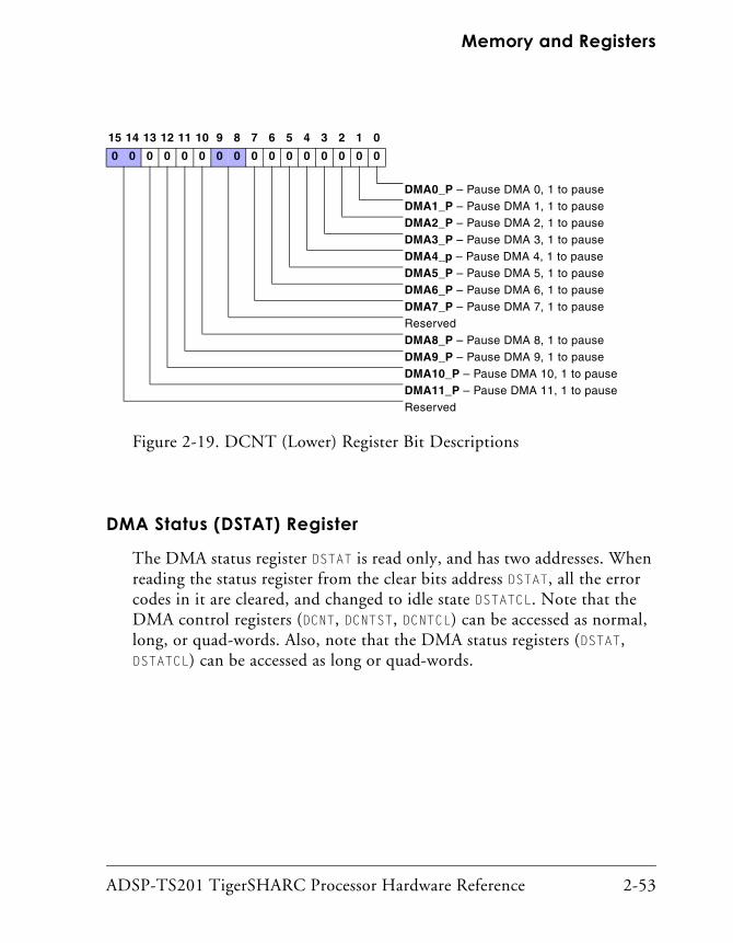
ADSP-TS201 TigerSHARC Processor Hardware Reference 2-53
Memory and Registers
DMA Status (DSTAT) Register
The DMA status register DSTAT is read only, and has two addresses. When reading the status register from the clear bits address DSTAT, all the error codes in it are cleared, and changed to idle state DSTATCL. Note that the DMA control registers (DCNT, DCNTST, DCNTCL) can be accessed as normal, long, or quad-words. Also, note that the DMA status registers (DSTAT, DSTATCL) can be accessed as long or quad-words.
15 14 13 12 11 10 9 8 7 6 5 4 3 2 1 0
0 0 0 0 0 0 0 0 0 0 0 0 0 0 0 0
DMA0_P – Pause DMA 0, 1 to pause DMA1_P – Pause DMA 1, 1 to pauseDMA2_P – Pause DMA 2, 1 to pauseDMA3_P – Pause DMA 3, 1 to pauseDMA4_p – Pause DMA 4, 1 to pauseDMA5_P – Pause DMA 5, 1 to pauseDMA6_P – Pause DMA 6, 1 to pauseDMA7_P – Pause DMA 7, 1 to pauseReservedDMA8_P – Pause DMA 8, 1 to pauseDMA9_P – Pause DMA 9, 1 to pauseDMA10_P – Pause DMA 10, 1 to pauseDMA11_P – Pause DMA 11, 1 to pauseReserved
Figure 2-19. DCNT (Lower) Register Bit Descriptions

Universal (Ureg) Register Space
2-54 ADSP-TS201 TigerSHARC Processor Hardware Reference
63 62 61 60 59 58 57 56 55 54 53 52 51 50 49 48
0 0 0 0 0 0 0 0 0 0 0 0 0 0 0 0
ReservedCH13 – DMA channel 13 statusCH12 – DMA channel 12 statusReserved
Figure 2-20. DSTATH (Upper) Register Bit Descriptions
31 30 29 28 27 26 25 24 23 22 21 20 19 18 17 16
0 0 0 0 0 0 0 0 0 0 0 0 0 0 0 0
ReservedCH7 – DMA channel 7 statusCH6 – DMA channel 6 statusCH5 – DMA channel 5 status
Bits17-15 continued on Figure 2-23
Figure 2-21. DSTATL (Upper) Register Bit Descriptions

ADSP-TS201 TigerSHARC Processor Hardware Reference 2-55
Memory and Registers
47 46 45 44 43 42 41 40 39 38 37 36 35 34 33 32
0 0 0 0 0 0 0 0 0 0 0 0 0 0 0 0
CH8 – DMA channel 8 statusCH9 – DMA channel 8 statusCH10 – DMA channel 10 statusCH11 – DMA channel 11 statusReserved
Figure 2-22. DSTATH (Lower) Register Bit Descriptions
15 14 13 12 11 10 9 8 7 6 5 4 3 2 1 0
0 0 0 0 0 0 0 0 0 0 0 0 0 0 0 0
CH0 – DMA channel 0 status;000 – Channel disabled001 – Block transfer in progress010 – Block transfer completed011 – Reserved
100 – Initialization of an active TCB1
101 – Illegal configuration in TCB2
110 – Reserved
111 – Address error – broadcast read3
1 CHx=100 status occurs for initialization of an active TCB with an active value. Clear this status by reading from the DSTATC register.
2 CHx=101 status could be as a result of setting the incorrect type field for an AutoDMA channel. Clear this status by reading from the DSTATC register.
3 CHx=111 status occurs if a source TCB address field is in the range 0x1C000000–0x1FFFFFFF
CH1 – DMA channel 1 statusCH2 – DMA channel 2 statusCH3 – DMA channel 3 statusCH4 – DMA channel 4 status
Bits17-15 continued on Figure 2-21 CH5 – DMA channel 5 status
Figure 2-23. DSTATL (Lower) Register Bit Descriptions

Universal (Ureg) Register Space
2-56 ADSP-TS201 TigerSHARC Processor Hardware Reference
External Port DMA TCB Register GroupNote that DMA registers can be accessed only as quad-words.
Table 2-21. External Port DMA TCB Register Group
Name Description Address Default
DCS0:DI DMA chan. 0 source TCB, index 0x1F 0000 0x0000 0000
DCS0:DX DMA chan.l 0 source TCB, x-dim 0x1F 0001 0x0100 0004
DCS0:DY DMA chan. 0 source TCB, y-dim 0x1F 0002 0x0000 0000
DCS0:DP DMA chan. 0 source TCB, prog. 0x1F 0003 0xD300 00001
DCD0:DI DMA chan. 0 destin. TCB, index 0x1F 0004 0x0000 0000
DCD0:DX DMA chan. 0 destin. TCB, x-dim 0x1F 0005 0x0100 0004
DCD0:DY DMA chan. 0 destin. TCB, y-dim 0x1F 0006 0x0000 0000
DCD0:DP DMA chan. 0 destin. TCB, prog. 0x1F 0007 0x5300 00001
DCS1:DI DMA chan. 1 source TCB, index 0x1F 0008 Undefined
DCS1:DX DMA chan. 1 source TCB, x-dim 0x1F 0009 Undefined
DCS1:DY DMA chan. 1 source TCB, y-dim 0x1F 000A Undefined
DCS1:DP DMA chan. 1 source TCB, prog. 0x1F 000B Undefined
DCD1:DI DMA chan. 1 destin. TCB, index 0x1F 000C Undefined
DCD1:DX DMA chan. 1 destin. TCB, x-dim 0x1F 000D Undefined
DCD1:DY DMA chan. 1 destin. TCB, y-dim 0x1F 000E Undefined
DCD1:DP DMA chan. 1 destin. TCB, prog. 0x1F 000F Undefined
DCS2:DI DMA chan. 2 source TCB, index 0x1F 0010 Undefined
DCS2:DX DMA chan. 2 source TCB, x-dim 0x1F 0011 Undefined
DCS2:DY DMA chan. 2 source TCB, y-dim 0x1F 0012 Undefined
DCS2:DP DMA chan. 2 source TCB, prog. 0x1F 0013 Undefined
DCD2:DI DMA chan. 2 destin. TCB, index 0x1F 0014 Undefined

ADSP-TS201 TigerSHARC Processor Hardware Reference 2-57
Memory and Registers
Link Port Transmit DMA TCB Register GroupNote that DMA registers can be accessed only as quad-words.
DCD2:DX DMA chan. 2 destin. TCB, x-dim 0x1F 0015 Undefined
DCD2:DY DMA chan. 2 destin. TCB, y-dim 0x1F 0016 Undefined
DCD2:DP DMA chan. 2 destin. TCB, prog. 0x1F 0017 Undefined
DCS3:DI DMA chan. 3 source TCB, index 0x1F 0018 Undefined
DCS3:DX DMA chan. 3 source TCB, x-dim 0x1F 0019 Undefined
DCS3:DY DMA chan. 3 source TCB, y-dim 0x1F 001A Undefined
DCS3:DP DMA chan. 3 source TCB, prog. 0x1F 001B Undefined
DCD3:DI DMA chan. 3 destin. TCB, index 0x1F 001C Undefined
DCD3:DX DMA chan. 3 destin. TCB, x-dim 0x1F 001D Undefined
DCD3:DY DMA chan. 3 destin. TCB, y-dim 0x1F 001E Undefined
DCD3:DP DMA chan. 3 destin. TCB, prog. 0x1F 001F Undefined
1 This default value only applies when EPROM boot mode select is active. Otherwise, the TY field is zero.
Table 2-22. Link Tx DMA TCB Register Group
Name Description Address Default
DC4:DI DMA channel 4 TCB, index 0x1F 0020 Undefined
DC4:DX DMA channel 4 TCB, x-dim 0x1F 0021 Undefined
DC4:DY DMA channel 4 TCB, y-dim 0x1F 0022 Undefined
DC4:DP DMA channel 4 TCB, prog. 0x1F 0023 Undefined
DC5:DI DMA channel 5 TCB, index 0x1F 0024 Undefined
DC5:DX DMA channel 5 TCB, x-dim 0x1F 0025 Undefined
Table 2-21. External Port DMA TCB Register Group (Cont’d)
Name Description Address Default
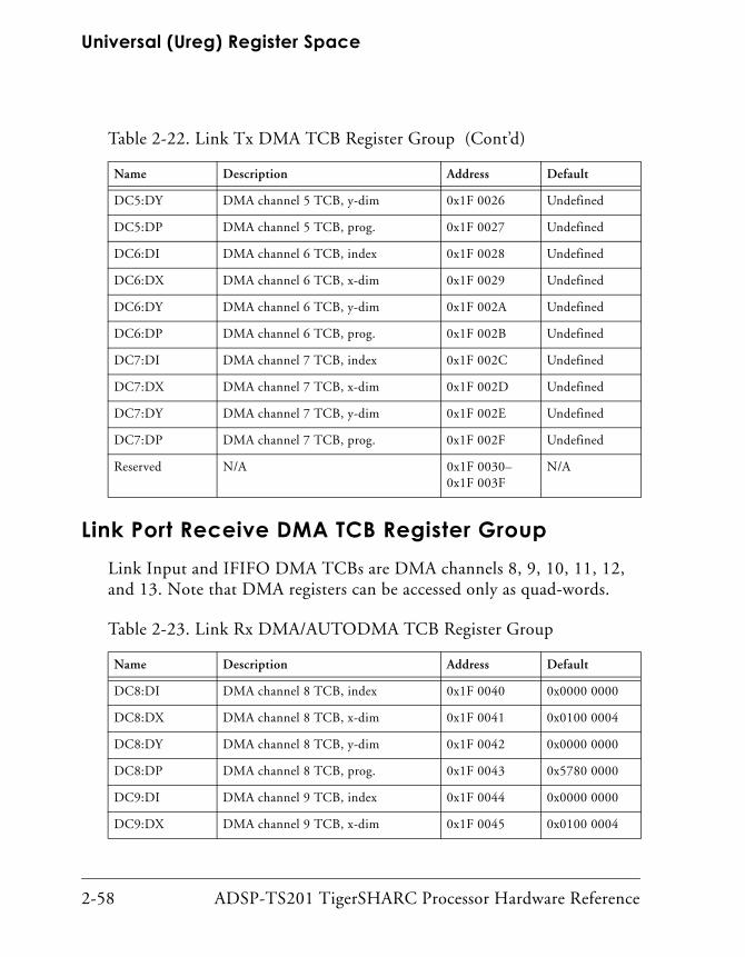
Universal (Ureg) Register Space
2-58 ADSP-TS201 TigerSHARC Processor Hardware Reference
Link Port Receive DMA TCB Register GroupLink Input and IFIFO DMA TCBs are DMA channels 8, 9, 10, 11, 12, and 13. Note that DMA registers can be accessed only as quad-words.
DC5:DY DMA channel 5 TCB, y-dim 0x1F 0026 Undefined
DC5:DP DMA channel 5 TCB, prog. 0x1F 0027 Undefined
DC6:DI DMA channel 6 TCB, index 0x1F 0028 Undefined
DC6:DX DMA channel 6 TCB, x-dim 0x1F 0029 Undefined
DC6:DY DMA channel 6 TCB, y-dim 0x1F 002A Undefined
DC6:DP DMA channel 6 TCB, prog. 0x1F 002B Undefined
DC7:DI DMA channel 7 TCB, index 0x1F 002C Undefined
DC7:DX DMA channel 7 TCB, x-dim 0x1F 002D Undefined
DC7:DY DMA channel 7 TCB, y-dim 0x1F 002E Undefined
DC7:DP DMA channel 7 TCB, prog. 0x1F 002F Undefined
Reserved N/A 0x1F 0030–0x1F 003F
N/A
Table 2-23. Link Rx DMA/AUTODMA TCB Register Group
Name Description Address Default
DC8:DI DMA channel 8 TCB, index 0x1F 0040 0x0000 0000
DC8:DX DMA channel 8 TCB, x-dim 0x1F 0041 0x0100 0004
DC8:DY DMA channel 8 TCB, y-dim 0x1F 0042 0x0000 0000
DC8:DP DMA channel 8 TCB, prog. 0x1F 0043 0x5780 0000
DC9:DI DMA channel 9 TCB, index 0x1F 0044 0x0000 0000
DC9:DX DMA channel 9 TCB, x-dim 0x1F 0045 0x0100 0004
Table 2-22. Link Tx DMA TCB Register Group (Cont’d)
Name Description Address Default

ADSP-TS201 TigerSHARC Processor Hardware Reference 2-59
Memory and Registers
DC9:DY DMA channel 9 TCB, y-dim 0x1F 0046 0x0000 0000
DC9:DP DMA channel 9 TCB, prog. 0x1F 0047 0x5780 0000
DC10:DI DMA channel 10 TCB, index 0x1F 0048 0x0000 0000
DC10:DX DMA channel 10 TCB, x-dim 0x1F 0049 0x0100 0004
DC10:DY DMA channel 10 TCB, y-dim 0x1F 004A 0x0000 0000
DC10:DP DMA channel 10 TCB, prog. 0x1F 004B 0x5780 0000
DC11:DI DMA channel 11 TCB, index 0x1F 004C 0x0000 0000
DC11:DX DMA channel 11 TCB, x-dim 0x1F 004D 0x0100 0004
DC11:DY DMA channel 11 TCB, y-dim 0x1F 004E 0x0000 0000
DC11:DP DMA channel 11 TCB, prog. 0x1F 004F 0x5780 0000
Reserved N/A 0x1F 0050–0x1F 0057
N/A
DC12:DI DMA channel 12 TCB, index 0x1F 0058 0x0000 0000
DC12:DX DMA channel 12 TCB, x-dim 0x1F 0059 0x0100 0001
DC12:DY DMA channel 12 TCB, y-dim 0x1F 005A 0x0000 0000
DC12:DP DMA channel 12 TCB, prog. 0x1F 005B 0x5380 0000
DC13:DI DMA channel 13 TCB, index 0x1F 005C 0x0000 0000
DC13:DX DMA channel 13 TCB, x-dim 0x1F 005D 0x0100 0001
DC13:DY DMA channel 13 TCB, y-dim 0x1F 005E 0x0000 0000
DC13:DP DMA channel 13 TCB, prog. 0x1F 005F 0x5380 0000
Table 2-23. Link Rx DMA/AUTODMA TCB Register Group (Cont’d)
Name Description Address Default

Universal (Ureg) Register Space
2-60 ADSP-TS201 TigerSHARC Processor Hardware Reference
AutoDMA Register GroupThe AutoDMA registers are used to implement a slave mode DMA (see “Direct Memory Access” on page 7-1). These registers can only be accessed through multiprocessing memory.
The AutoDMA channel 0 data registers (listed in appear in Table 2-24) contain 32-, 64-, or 128-bit data. When writing to this register, DMA channel 12 transfers the written data into the internal memory address programmed in the DMA. This register cannot be read, and can only be written through the multiprocessing address space. If the DMA is not ini-tialized, the data is lost.
The AutoDMA channel 1 data registers (listed in appear in Table 2-24) contain 32-, 64-, or 128-bit data. When writing to this register, DMA channel 13 transfers the written data into the internal memory address programmed in the DMA. This register cannot be read, and can only be written through the multiprocessing address space. If the DMA is not ini-tialized, the data is lost.
Table 2-24. AUTO DMA Register Group
Name Description Address Default
AUTODMA0:0 AutoDMA reg 0, data bits 31–0 0x1F 03E0 N/A
AUTODMA0:1 AutoDMA reg 0, data bits 63–32 0x1F 03E1 N/A
AUTODMA0:2 AutoDMA reg 0, data bits 95–64 0x1F 03E2 N/A
AUTODMA0:3 AutoDMA reg 0, data bits 127–96 0x1F 03E3 N/A
AUTODMA1:0 AutoDMA reg 1, data bits 31–0 0x1F 03E4 N/A
AUTODMA1:1 AutoDMA reg 1, data bits 63–32 0x1F 03E5 N/A
AUTODMA1:2 AutoDMA reg 1, data bits 95–64 0x1F 03E6 N/A
AUTODMA1:3 AutoDMA reg 1, data bits 127–96 0x1F 03E7 N/A
Reserved N/A 0x1F 03E8–0x1F 03FF
N/A

ADSP-TS201 TigerSHARC Processor Hardware Reference 2-61
Memory and Registers
DMA Index (DI), X-Dimension (DX),Y-Dimension (DY), and Pointer (DP) TCB Registers
Each of the four external memory DMA channels is controlled by a trans-fer control block (TCB) quad-word register pair. In addition, each of the four link ports to or from memory DMA channels is controlled by a TCB quad-word register. Finally, each of the two AutoDMA registers-to-mem-ory DMA channels is controlled by a TCB quad-word register. The registers that make up the TCBs are:
DMA index (DIx) register
This is the 32-bit Index register for the DMA. It can point to the address of external, internal memory, or link ports. (See Figure 2-24 and Figure 2-27.)
DMA X dimension (DXx) register
If a two-dimensional (2D) DMA is disabled, this register contains the 16-bit modify (LSBs) and 16-bit count (MSBs) values for the DMA. If a two-dimensional (2D) DMA is enabled, it contains the 16-bit modify and 16-bit count X dimension values. (See Figure 2-25 and Figure 2-28.) For some transfer types (TY bits in DPx register equal 011 or 111), the DXx holds a 10-bit count (MSBs) and 22-bit modify (LSBs).
DMA Y dimension (DYx) register
This register is used together with the DX register when a two-dimensional DMA is enabled. It contains the 16-bit modify and the 16-bit Y count dimension values. (See Figure 2-26 and Figure 2-29.) For some transfer types (TY bits in DPx register equal 011 or 111), the DYx holds a 10-bit count (MSBs) and 22-bit modify (LSBs).
For more information on using the TCB registers for DMA (and more details on the bits in the DIx, DXx, DYx, and DPx registers), see “Setting Up DMA Transfers” on page 7-15.

Universal (Ureg) Register Space
2-62 ADSP-TS201 TigerSHARC Processor Hardware Reference
31 30 29 28 27 26 25 24 23 22 21 20 19 18 17 16
0 0 0 0 0 0 0 0 0 0 0 0 0 0 0 0
ADDR – Source/Destination AddressBits continued on Figure 2-27
Figure 2-24. DI (DMA Index, Upper) Register Bit Descriptions
31 30 29 28 27 26 25 24 23 22 21 20 19 18 17 16
0 0 0 0 0 0 0 0 0 0 0 0 0 0 0 0
CNT – X Count Value
Figure 2-25. DX (DMA X Dimension, Upper) Register Bit Descriptions
31 30 29 28 27 26 25 24 23 22 21 20 19 18 17 16
0 0 0 0 0 0 0 0 0 0 0 0 0 0 0 0
CNT – Y Count Value
Figure 2-26. DY (DMA Y Dimension, Upper) Register Bit Descriptions

ADSP-TS201 TigerSHARC Processor Hardware Reference 2-63
Memory and Registers
DMA chaining pointer (DPx) register
This register is split into two fields, where the first is dedicated to DMA control and the second is dedicated to chaining. (See Figure 2-30.)
15 14 13 12 11 10 9 8 7 6 5 4 3 2 1 0
0 0 0 0 0 0 0 0 0 0 0 0 0 0 0 0
ADDR – Source/Destination AddressBits continued on Figure 2-24
Figure 2-27. DI (DMA Index, Lower) Register Bit Descriptions
15 14 13 12 11 10 9 8 7 6 5 4 3 2 1 0
0 0 0 0 0 0 0 0 0 0 0 0 0 0 0 0
MOD – X Modify Value
Figure 2-28. DX (DMA X Dimension, Lower) Register Bit Descriptions
15 14 13 12 11 10 9 8 7 6 5 4 3 2 1 0
0 0 0 0 0 0 0 0 0 0 0 0 0 0 0 0
MOD – Y Modify Value
Figure 2-29. DY (DMA Y Dimension, Lower) Register Bit Descriptions

Universal (Ureg) Register Space
2-64 ADSP-TS201 TigerSHARC Processor Hardware Reference
31 30 29 28 27 26 25 24 23 22 21 20 19 18 17 16
0 0 0 0 0 0 0 0 0 0 0 0 0 0 0 0
TY – Specifies the device type;000 – DMA disabled
001 – I/O link port DMA010 – Internal memory
011 – Internal memory (larger stride)100 – External memory
101 – External I/O device (Flyby)110 – Boot EPROM
111 – External memory (larger stride)PR – Determines priority ;
1=high. 0=normal2DDMA – Two-dimensional DMA;
1=2 dimensional, 0=1 dimensionalLEN – Operand length;
00 – Reserved01 – Normal (32-bit) word
10 – Long (64-bit) word11 – Quad (128-bit) word
INT – Interrupt enable;1=enabled, 0=disabled
DRQ – DMA request enable1=enabled, 0=disabled
CHEN – Chaining enabled1=enabled, 0=disabledCHTG – Chaining destination channel;
000 – Link Receive Channel 0001 – Link Receive Channel 1010 – Link Receive Channel 2011 – Link Receive Channel 3100 – Link Transmit Channel 0101 – Link Transmit Channel 1110 – Link Transmit Channel 2111 – Link Transmit Channel 3
CHPT – Chain pointer address1
1 The CHPT field includes bits 18–0 (bits 15–0 not shown).
Figure 2-30. DPx (Upper) Register Bit Descriptions

ADSP-TS201 TigerSHARC Processor Hardware Reference 2-65
Memory and Registers
Link Port Register GroupsThe Link Port Buffer registers are only accessible as quad words. There are two Link register groups described in Table 2-25 and Table 2-26. Link Control and Status registers can be accessed only as single words. See “Link Ports” on page 9-1 for complete Link register definitions.
Table 2-25. Link Port Receive/Transmit Buffer Register Group
Name Description Address Default
LBUFTX0:0 Link # 0 Tx data 0x1F 04A0 Undefined
LBUFTX0:1 Link # 0 Tx data 0x1F 04A1 Undefined
LBUFTX0:2 Link # 0 Tx data 0x1F 04A2 Undefined
LBUFTX0:3 Link # 0 Tx data 0x1F 04A3 Undefined
LBUFRX0:0 Link # 0 Rx data; Read only 0x1F 04A4 Undefined
LBUFRX0:1 Link # 0 Rx data; Read only 0x1F 04A5 Undefined
LBUFRX0:2 Link # 0 Rx data; Read only 0x1F 04A6 Undefined
LBUFRX0:3 Link # 0 Rx data; Read only 0x1F 04A7 Undefined
LBUFTX1:0 Link # 1 Tx data 0x1F 04A8 Undefined
LBUFTX1:1 Link # 1 Tx data 0x1F 04A9 Undefined
LBUFTX1:2 Link # 1 Tx data 0x1F 04AA Undefined
LBUFTX1:3 Link # 1 Tx data 0x1F 04AB Undefined
LBUFRX1:0 Link # 1 Rx data; Read only 0x1F 04AC Undefined
LBUFRX1:1 Link # 1 Rx data; Read only 0x1F 04AD Undefined
LBUFRX1:2 Link # 1 Rx data; Read only 0x1F 04AE Undefined
LBUFRX1:3 Link # 1 Rx data; Read only 0x1F 04AF Undefined
LBUFTX2:0 Link # 2 Tx data 0x1F 04B0 Undefined
LBUFTX2:1 Link # 2 Tx data 0x1F 04B1 Undefined
LBUFTX2:2 Link # 2 Tx data 0x1F 04B2 Undefined

Universal (Ureg) Register Space
2-66 ADSP-TS201 TigerSHARC Processor Hardware Reference
LBUFTX2:3 Link # 2 Tx data 0x1F 04B3 Undefined
LBUFRX2:0 Link # 2 Rx data; Read only 0x1F 04B4 Undefined
LBUFRX2:1 Link # 2 Rx data; Read only 0x1F 04B5 Undefined
LBUFRX2:2 Link # 2 Rx data; Read only 0x1F 04B6 Undefined
LBUFRX2:3 Link # 2 Rx data; Read only 0x1F 04B7 Undefined
LBUFTX3:0 Link # 3 Tx data 0x1F 04B8 Undefined
LBUFTX3:1 Link # 3 Tx data 0x1F 04B9 Undefined
LBUFTX3:2 Link # 3 Tx data 0x1F 04BA Undefined
LBUFTX3:3 Link # 3 Tx data 0x1F 04BB Undefined
LBUFRX3:0 Link # 3 Rx data; Read only 0x1F 04BC Undefined
LBUFRX3:1 Link # 3 Rx data; Read only 0x1F 04BD Undefined
LBUFRX3:2 Link # 3 Rx data; Read only 0x1F 04BE Undefined
LBUFRX3:3 Link # 3 Rx data; Read only 0x1F 04BF Undefined
Table 2-26. Link Control and Status Register Group
Name Description Address Default
LRCTL0 Link # 0 Rx control 0x1F 00E0 0x0000 0001(or 0x0000 0011)
LRCTL1 Link # 1 Rx control 0x1F 00E1 0x0000 0001(or 0x0000 0011)
LRCTL2 Link # 2 Rx control 0x1F 00E2 0x0000 0001(or 0x0000 0011)
LRCTL3 Link # 3 Rx control 0x1F 00E3 0x0000 0001(or 0x0000 0011)
LTCTL0 Link # 0 Tx control 0x1F 00E4 0x0000 0000
LTCTL1 Link # 1 Tx control 0x1F 00E5 0x0000 0000
Table 2-25. Link Port Receive/Transmit Buffer Register Group (Cont’d)
Name Description Address Default

ADSP-TS201 TigerSHARC Processor Hardware Reference 2-67
Memory and Registers
LTCTL2 Link # 2 Tx control 0x1F 00E6 0x0000 0000
LTCTL3 Link # 3 Tx control 0x1F 00E7 0x0000 0000
Reserved N/A 0x1F 00E6–0x1F 00EF
N/A
LRSTAT0 Link # 0 Rx status 0x1F 00F0 0x0000 0000
LRSTAT1 Link # 1 Rx status 0x1F 00F1 0x0000 0000
LRSTAT2 Link # 2 Rx status 0x1F 00F2 0x0000 0000
LRSTAT3 Link # 3 Rx status 0x1F 00F3 0x0000 0000
LTSTAT0 Link # 0 Tx status 0x1F 00F4 0x0000 0002
LTSTAT1 Link # 1 Tx status 0x1F 00F5 0x0000 0002
LTSTAT2 Link # 2 Tx status 0x1F 00F6 0x0000 0002
LTSTAT3 Link # 3 Tx status 0x1F 00F7 0x0000 0002
LRSTATC0 Link # 0 Rx status clear 0x1F 00F8 Undefined
LRSTATC1 Link # 1 Rx status clear 0x1F 00F9 Undefined
LRSTATC2 Link # 2 Rx status clear 0x1F 00FA Undefined
LRSTATC3 Link # 3 Rx status clear 0x1F 00FB Undefined
LTSTATC0 Link # 0 Tx status clear 0x1F 00FC Undefined
LTSTATC1 Link # 1 Tx status clear 0x1F 00FD Undefined
LTSTATC2 Link # 2 Tx status clear 0x1F 00FE Undefined
LTSTATC3 Link # 3 Tx status clear 0x1F 00FF Undefined
Table 2-26. Link Control and Status Register Group (Cont’d)
Name Description Address Default

Universal (Ureg) Register Space
2-68 ADSP-TS201 TigerSHARC Processor Hardware Reference
Link Receive Control (LRCTLx) Registers
The LRCTLx registers setup receive features for link ports. The LRCTLx reg-isters’ reset value is 0x0000 0001, when the LINK_DWIDTH strap pin =0 at reset (RDSIZE=0). When the LINK_DWIDTH strap pin =1 at reset, the LRCTLx registers’ reset value is 0x0000 0011 (RDSIZE=1).
15 14 13 12 11 10 9 8 7 6 5 4 3 2 1 0
0 0 0 0 0 0 0 0 0 0 0 0 0 0 0 1
REN Receive Enable1=enable, 0=disable
RVERE Verification Enable1=enable, 0=disable
RTOE Receive Time Out Check IRQ Enable1=enable, 0=disable
RBCMPE Receive Block Completion1=enable LxBCMPI input detection,0=disable LxBCMPI input detection
RDSIZE Data Size1 1=4 bit data, 0=1 bit data
1 The reset value of the RDSIZE bit depends on the value of the LINK_DWIDTH strap pin at reset. If LINK_DWIDTH=0 at reset, RDSIZE=0 (1 bit data).
ROVRE Receive Overrun Error IRQ Enable1=enable, 0=disable
RINIF Receive Initialization Forced1=force RINIV value, 0=not forced
RINIV Receive Initialization Value1=use 1 for data, 0=use 0 for data
Reserved
Figure 2-31. LRCTLx Low (Lower) Register Bit Descriptions2
2 The upper 16 bits (31–16) of LRCTLx are reserved (=0)

ADSP-TS201 TigerSHARC Processor Hardware Reference 2-69
Memory and Registers
Link Transmit Control (LTCTLx) Registers
The LTCTLx registers setup transmit features for link ports. The LTCTLx registers’ reset value is 0x0000 0001.
15 14 13 12 11 10 9 8 7 6 5 4 3 2 1 0
0 0 0 0 0 0 0 0 0 0 0 0 0 0 0 0
TEN Transmit Enable1=enable, 0=disable
TVERE Verification Enable1= enable, 0=disable
TTOE Transmit Time Out check IRQ Enable1=enable, 0=disable
TBCMPE Transmit Block Completion1=enable LxBCMPO output,0=disable LxBCMPO output
TDSIZE Data Size 1 = 4 bit data, 0 = 1 bit data
SPD Transfer Speed.Sets LxCLKOUT divisor from CCLK:000: divide CCLK by 1001: divide CCLK by 1.5010: divide CCLK by 2100: divide CCLK by 4011: (reserved)101: (reserved)110: (reserved)111: (reserved)
Reserved (DLLV3–0)Reserved
Figure 2-32. LTCTLx Low (Lower) Register Bit Descriptions1
1 The upper 16 bits (31–16) of LTCTLx are reserved (=0)

Universal (Ureg) Register Space
2-70 ADSP-TS201 TigerSHARC Processor Hardware Reference
Link Receive Status (LRSTATx) Registers
The LRSTATx registers indicate receive status for link ports. The LRSTATx registers’ reset value is 0x0000 0000.
15 14 13 12 11 10 9 8 7 6 5 4 3 2 1 0
0 0 0 0 0 0 0 0 0 0 0 0 0 0 0 0
RSTAT Receive buffers status00: buffer empty01: buffer valid (can still receive)11: buffer full10: buffer not ready (data transient)
RTER Receive timeout error indication1=error, 0=no error
RWER Receive write error1=error, 0=no error
RCSER Receiver checksum error1=error, 0=no error
ROVER Receive overrun error1=error, 0=no error
RINIT Receiver initialization status1=initialized, 0=not initialized
Reserved
Figure 2-33. LRSTATx Low (Lower) Register Bit Descriptions1
1 The upper 16 bits (31–16) of LRSTATx are reserved (=0)

ADSP-TS201 TigerSHARC Processor Hardware Reference 2-71
Memory and Registers
Link Transmit Status (LTSTATx) Registers
The LTSTATx registers indicate transmit status for link ports. The LTSTATx registers’ reset value is 0x0000 0002.
15 14 13 12 11 10 9 8 7 6 5 4 3 2 1 0
0 0 0 0 0 0 0 0 0 0 0 0 0 0 1 0
TVACANT Transmit Buffer Vacant1
1=transmit buffer vacant (buffer writable)0=transmit buffer not vacant (not writable)
1 TVACANT=1 indicates that the buffer is vacant, and the transmit DLL is locked. After enabling the transmitter (LTEN=1 in LTCTLx), the transmit DLL requires up to 800 SOCCLK cycles to stabilize.
TEMPTY Transmit Buffer Empty2
1=transmit buffer empty (buf. transmitted)0=transmit buffer not empty
2 TEMPTY should be tested for buffer transmitted before disabling the channel.
TTER Transmit Timeout Error1=error, 0=no error
TWER Transmit Write Error1=error, 0=no error
Reserved
Figure 2-34. LTSTATx Low (Lower) Register Bit Descriptions3
3 The upper 16 bits (31–16) of LTSTATx are reserved (=0)

Universal (Ureg) Register Space
2-72 ADSP-TS201 TigerSHARC Processor Hardware Reference
External Bus Interface Register GroupsThe external port registers appear in Table 2-27.
Table 2-27. Bus Interface Unit Register Group
Name Description Address Default
SYSCON System configuration register 0x1F 0080 0xXX00 9067
Reserved N/A 0x1F 0081–0x1F 0082
N/A
BUSLOCK System control register 0x1F 0083 See Definition
SDRCON SDRAM configuration register (see “SDRAM Programming” on page 8-67)
0x1F 0084 See Definition
Reserved N/A 0x1F 0085 N/A
SYSTAT System status register; Read only 0x1F 0086 See Definition
SYSTATCL System status register; destructive address (clear error); Read only
0x1F 0087 Undefined
Reserved N/A 0x1F 0088–0x1F 008B
N/A
BMAX Maximum cycle count for bus fairness (see “Bus Fairness (BMAX) Register” on page 8-44)
0x1F 008C See Definition
BMAXC Current count on BMAX; Read only 0x1F 008D Undefined
Reserved N/A 0x1F 008E–0x1F 009F
N/A

ADSP-TS201 TigerSHARC Processor Hardware Reference 2-73
Memory and Registers
System Configuration (SYSCON) Register
The SYSCON register defines bus control configuration. The SYSCON regis-ter’s reset value = 0xXX00 9067 (where XX—bits 22–31—are undefined). The processor’s mode (User or Supervisor) and the reset state of the SYS_REG_WE strap pin control write access to the SYSCON register. In User mode with the SYS_REG_WE strap pin disabled at reset, the SYSCON register can be written only once after hardware reset and cannot be changed dur-ing system operation—subsequent writes to SYSCON are ignored.
To write to the SYSCON register (and SDRCON register) more than once after reset in User mode, enable the SYS_REG_WE strap pin during reset. In Supervisor mode, SYSCON and SDRCON have no write restrictions.
The bit descriptions for this register are shown in Figure 2-35 and Figure 2-36. For more information on using this register, see “SYSCON Register Programming” on page 8-13. Note that bits 22-31 are undefined.

Universal (Ureg) Register Space
2-74 ADSP-TS201 TigerSHARC Processor Hardware Reference
31 30 29 28 27 26 25 24 23 22 21 20 19 18 17 16
0 0 0 0 0 0 0 0 0 0 0 0 0 0 0 0
ReservedHSTWIDTH – Host Bus Width
1=64 bits wide0=32 bits wide
MPWIDTH – Multiprocessing Bus Width1=64 bits wide0=32 bits wide
MEMWIDTH – Memory Bus Width1=64 bits wide0=32 bits wide
ReservedHOSTSLOW – Host Slow Protocol Bit
(See BNK0SLOW bit definition.)HOSTPIPE – Host Pipe Depth Bits
(See BNK0PIPE bits definition.)Bit 15 continued in Figure 2-36
Figure 2-35. SYSCON (Upper) Register Bit Descriptions

ADSP-TS201 TigerSHARC Processor Hardware Reference 2-75
Memory and Registers
15 14 13 12 11 10 9 8 7 6 5 4 3 2 1 0
1 0 0 1 0 0 0 0 0 1 1 0 0 1 1 1
BNK0IDLE – Memory Bank 0 Idle1=insert idle cycle between transactions0=no idle insertion
BNK0WAIT – Memory Bank 0 Internal Wait00=0 wait cycles01=1 wait cycle10=2 wait cycles11=3 wait cycles
BNK0PIPE – Memory Bank 0 Pipe Depth1
00=1 cycle pipe depth01=2 cycles pipe depth10=3 cycles pipe depth11=4 cycles pipe depthSame definitions as Host bits
BNK0SLOW – Memory Bank 0 Slow Protocol1=slow protocol active 0=synchronous and pipelined
BNK1IDLE – Memory Bank 1 Idle(See BNK0IDLE bit definition.)
BNK1WAIT – Memory Bank 1 Interval Wait(See BNK0WAIT bits definition.)
BNK1PIPE – Memory Bank 1 Pipe Depth(See BNK0PIPE bits definition.)
BNK1SLOW – Memory Bank 1 Slow Protocol(See BNK0SLOW bit definition.)
HOSTIDLE – Host Idle Bit(See BNK0IDLE bit definition.)
HOSTWAIT –Host Interval Wait Bits(See BNK0WAIT bits definition.)
Bit 16 continued in Figure 2-35 HOSTPIPE – Host Pipe Depth Bits(See BNK0PIPE bits definition.)
Figure 2-36. SYSCON (Lower) Register Bit Descriptions1 If using slow protocol, BNKx/HOSTPIPE bit is cleared.

Universal (Ureg) Register Space
2-76 ADSP-TS201 TigerSHARC Processor Hardware Reference
Bus Lock (BUSLOCK) System Control Register
The BUSLOCK register defines the bus lock status. The BUSLOCK register’s reset value is 0xXX00 0000 (where XX is undefined). Note that bits 22-31 are undefined.
SDRAM Configuration (SDRCON) Register
The SDRCON register defines SDRAM configuration. The SDRCON register’s reset value is 0xXX00 0000 (where XX is undefined). Note that this reset value indicates that at reset SDRAM is disabled. The processor’s mode (User or Supervisor) and the reset state of the SYS_REG_WE strap pin con-trol write access to the SDRCON register. In User mode with the SYS_REG_WE strap pin disabled at reset, the SDRCON register can be written only once after hardware reset and cannot be changed during system operation—subsequent writes to SDRCON are ignored.
To write to the SDRCON register (and SYSCON register) more than once after reset in User mode, enable the SYS_REG_WE strap pin during reset. In Supervisor mode, SYSCON and SDRCON have no write restrictions.
The bit descriptions for this register are shown in Figure 2-38 on page 2-77. Note that bits 22–31 are undefined.
15 14 13 12 11 10 9 8 7 6 5 4 3 2 1 0
0 0 0 0 0 0 0 0 0 0 0 0 0 0 0 0
BUSLK – BUSLOCK status indicator1=request bus lock from current master0=no request
Reserved
Figure 2-37. BUSLOCK (Lower) Register Bit Descriptions1
1 The upper 16 bits (31–16) of BUSLOCK are reserved (=0)

ADSP-TS201 TigerSHARC Processor Hardware Reference 2-77
Memory and Registers
System Status (SYSTAT) Register
The SYSTAT register is a read-only register that indicates the system/bus status. The SYSTAT register’s reset value is 0xXX00 SS0S (where XX is undefined, and SS is strap pin).
15 14 13 12 11 10 9 8 7 6 5 4 3 2 1 0
0 0 0 0 0 0 0 0 0 0 0 0 0 0 0 0
SDREN – SDRAM Enable1=enable, 0=disable
CAS – CAS Latency00 = 1 cycle, 01 = 2 cycles10 = 3 cycles, 11 = Reserved
PIPE – Pipe Depth1=1 cycle, 0=0 cycles
PAGE – Page Boundary For Burst Brake00 = 256 words, 01 = 512 words10 = 1K words, 11 = Reserved
ReservedREF – Refresh Rate (in SCLK cycles)
00 = Every 1100 cycles (SOC 250MHz)01 = Every 1850 cycles (SOC 300MHz)10 = Every 2200 cycles (SOC 250MHz)11 = Every 3700 cycles (SOC 300MHz)
PRC2RAS – Precharge-to-RAS Delay00 = 2 cycles, 01 = 3 cycles,10 = 4 cycles, 11 = 5 cycles
RAS2PRC – RAS-to-Precharge Delay000 = 2 cycles, 001 = 3 cycles, 010 = 4 cycles, 011 = 5 cycles, 100 = 6 cycles, 101 = 7 cycles110 = 8 cycles
INIT – Initialization Sequence1 = MRS after SDRAM refresh0 – MRS before SDRAM refresh
EMREN – Extended Mode Register1 = enabled; EMRS cycle precedes MRS0 = disabled
Figure 2-38. SDRCON (Lower) Register Bit Descriptions1
1 Bits 31–16 (not shown) are reserved (=0).

Universal (Ureg) Register Space
2-78 ADSP-TS201 TigerSHARC Processor Hardware Reference
Programs can read the SYSTAT register using the name SYSTAT or SYSTATCL (SYSTAT clear). The register name (address) determines whether the error bits (19–16) are cleared after the read. Note that bits 22-31 are undefined. The bit descriptions for this register are shown in Figure 2-39 on page 2-78 and Figure 2-40 on page 2-79.
• SYSTAT – no change in register contents
• SYSTATCL – error Bits19–16 are cleared after the read
31 30 29 28 27 26 25 24 23 22 21 20 19 18 17 16
0 0 0 0 0 0 0 0 0 0 0 0 0 0 0 0
ReservedMPREADERR – Self Multiproc. Read Error
1 = error (illegal read from self using multiprocessor memory space)0 = no error
SDRAMERR – SDRAM Error1 = error (access made to non-initialized SDRAM)0 = no error
AUTODMAERR – AutoDMA Error1 = error (data is written to AutoDMA while channel not initialized)0 = no error
BRODREADERR – Broadcast Read Error1 = error (slave broadcast read by another master)0 = no error
Figure 2-39. SYSTAT/SYSTATCL (Upper) Register Bit Descriptions

ADSP-TS201 TigerSHARC Processor Hardware Reference 2-79
Memory and Registers
15 14 13 12 11 10 9 8 7 6 5 4 3 2 1 0
0 0 0 0 0 0 0 0 0 0 0 0 0 0 0 0
PROCID – Processor ID in systemIndicates value of ID2–0 pins
ReservedBUSMSTR – Current Bus Master
Indicates the ID of the current bus masterHSTMSTR – Host Master
1 = bus master is the host0 = bus master is not the host
CLCKMULT – SCLK to CCLK Clock multiplierIndicates value of SCLKRAT2–0 pins000 = CCLK is 4xSLCLK001 = CCLK is 5xSLCLK010 = CCLK is 6xSLCLK011 = CCLK is 7xSLCLK100 = CCLK is 8xSLCLK101 = CCLK is 10xSLCLK110 = CCLK is 12xSLCLK111 = Reserved
ReservedBOOTMDE – Boot Mode (EBOOT strap pin)
1 = boot other than EPROM0 = EPROM boot
MRSCOMP – MRS Complete (ID=000 only)1 = MRS complete (SDRAM access legal)0 = MRS not complete
BUSLKACT – BUSLK Active1=BUSLK bit is set (processor holds bus)0=BUSLK bit is not set
Reserved
Figure 2-40. SYSTAT/SYSTATCL (Lower) Register Bit Descriptions

Universal (Ureg) Register Space
2-80 ADSP-TS201 TigerSHARC Processor Hardware Reference
Bus Master Maximum (BMAX) Register
The BMAX register is set with the maximum number of internal clock cycles (CCLK) for which the TigerSHARC processor is allowed to retain master-ship on the external bus. When reading this address, the returned value is the value written to the BMAX register, not the current cycle count. When the BMAX initialization count (bits 15–0) is 0xFFFF, the BMAX counter is disabled. (See Figure 2-41 on page 2-80.) See “Bus Fairness (BMAX) Reg-ister” on page 8-44 for more information.
Bus Master Maximum Current Count (BMAXC) Register
This address is read-only and returns the BMAX counter value when read. The BMAXC register’s reset value = 0xXX00 FFFF (where XX is undefined). Note that bits 22-31 are undefined. (See Figure 2-42 on page 2-80.)
15 14 13 12 11 10 9 8 7 6 5 4 3 2 1 0
1 1 1 1 1 1 1 1 1 1 1 1 1 1 1 1
BMAX – Bus Master Max Initialization Count0xFFFF = count disabled0xFFFE ≥ bus master max count
Figure 2-41. BMAX (Lower) Register Bit Descriptions1
1 The upper 16 bits (31–16) of BMAX are reserved (=0)
15 14 13 12 11 10 9 8 7 6 5 4 3 2 1 0
1 1 1 1 1 1 1 1 1 1 1 1 1 1 1 1
BMAXC – Bus Master Max Current Count0xFFFF = count disabled0xFFFE ≥ bus master current count
Figure 2-42. BMAXC (Lower) Register Bit Descriptions1
1 The upper 16 bits (31–16) of BMAXC are reserved (=0)

ADSP-TS201 TigerSHARC Processor Hardware Reference 2-81
Memory and Registers
JTAG Test and Emulation Register Groups
Table 2-28. JTAG Register Group
Name Description Address Default
EMUCTL Emulation Control 0x1F 03A0 0x0000 0020
EMUSTAT Emulation Status 0x1F 03A1 0x0000 0020
EMUDAT Emulation Data 0x1F 03A2 Undefined
IDCODE ID Code 0x1F 03A3 0xX27A F0CB
EMUIR:0 Emulation Instruction 0 0x1F 03A4 0x33C0 0000
EMUIR:1 Emulation Instruction 1 0x1F 03A5 0x33C0 0000
EMUIR:2 Emulation Instruction 2 0x1F 03A6 0x33C0 0000
EMUIR:3 Emulation Instruction 3 0x1F 03A7 0xB3C0 0000
Reserved Reserved 0x1F 03A8 N/A
OSPID OSPID 0x1F 03A9 Undefined
Reserved Reserved 0x1F 03AA–0x1F 03BF N/A

Universal (Ureg) Register Space
2-82 ADSP-TS201 TigerSHARC Processor Hardware Reference
Emulation Control (EMUCTL) Register
The EMUCTL register sets up emulation features. The EMUCTL register’s reset value is 0x0000 0020. Most bits in the EMUCTL register are used by the emulator and should not be modified by programs. The only bits in the EMUCTL register that are intended for program usage are the SWRST (soft-ware reset) bit and the BOOTDIS (boot disable) bit. (See Figure 2-43 on page 2-82.)
15 14 13 12 11 10 9 8 7 6 5 4 3 2 1 0
0 0 0 0 0 0 0 0 0 0 1 0 0 0 0 0
EMEN – Emulation Enable1=enable, 0=disable
TEME – TMS Emulation Exception1=exception, 0=no exception
EMUOE – Emulation Output Enable1=enable, 0=disable
SPFDIS – SPF Disable1=disable, 0=enable
SWRST – Software Reset1=reset request, 0=no reset request
BOOTDSBL – Boot Disable1
1=disable, 0=enable
1 The BOOTDSBL bit is cleared on hardware reset, but not cleared on software reset
Reserved
Figure 2-43. EMUCTL (Lower) Register Bit Descriptions2
2 The upper 16 bits (31–16) of EMUCTL are reserved (=0)

ADSP-TS201 TigerSHARC Processor Hardware Reference 2-83
Memory and Registers
Emulation Status (EMUSTAT) Register
The EMUSTAT register indicates emulation status. The EMUCTL register’s reset value is 0x0000 0002. (See Figure 2-44 on page 2-83.)
Silicon Version and ID Code (IDCODE) Register
The IDCODE register indicates processor model ID and silicon version. The EMUCTL register’s reset value is 0xV27A F0CB (where V is version). (See Figure 2-45 on page 2-83.)
15 14 13 12 11 10 9 8 7 6 5 4 3 2 1 0
0 0 0 0 0 0 0 0 0 0 0 0 0 0 1 0
EMUMOD – Emulation Mode1=emulation, 0=not emulation
IRFREE – Emulation Instruction Register Free1=EMUIR ready, 0=EMUIR not ready
INRESET – Emulation Output Enable1=reset active, 0=no reset
Reserved
Figure 2-44. EMUSTAT (Lower) Register Bit Descriptions1
1 The upper 16 bits (31–16) of EMUSTAT are reserved (=0)
31 30 29 28 27 26 25 24 23 22 21 20 19 18 17 16
0 0 0 0 0 0 0 0 0 0 0 0 0 0 0 0
ID31–28 – Silicon Version
ID27–0 – IDCODE (0x27A F0CB)1
1 The ID27–0 field includes bits 27–0 (bits 15–0 not shown).
Figure 2-45. IDCODE (Upper) Register Bit Descriptions

Universal (Ureg) Register Space
2-84 ADSP-TS201 TigerSHARC Processor Hardware Reference
Debug Register GroupsThe debug groups are described in Table 2-29 on page 2-84. The debug registers can only be accessed as single-word registers. In emulation mode, the debug registers can be accessed only by move, register to register, or immediate data load instructions. These registers cannot be loaded from or stored to memory directly. There is a five cycle stall after any write to the debug group registers.
Table 2-29. Debug Register Group
Register Description Address Default
WP0CTL Watchpoint 0 control 0x1E 0360 0x0000 0000
WP1CTL Watchpoint 1 control 0x1E 0361 0x0000 0000
WP2CTL Watchpoint 2 control 0x1E 0362 0x0000 0000
Reserved N/A 0x1E 0363 N/A
WP0STAT Watchpoint 0 status; (RO) 0x1E 0364 0x0000 0000
WP1STAT Watchpoint 1 status; (RO) 0x1E 0365 0x0000 0000
WP2STAT Watchpoint 2 status; (RO) 0x1E 0366 0x0000 0000
Reserved N/A 0x1E 0367 N/A
WP0L Watchpoint 0 low address 0x1E 0368 Undefined
WP0H Watchpoint 0 high address 0x1E 0369 Undefined
WP1L Watchpoint 1 low address 0x1E 036A Undefined
WP1H Watchpoint 1 high address 0x1E 036B Undefined
WP2L Watchpoint 2 low address 0x1E 036C Undefined
WP2H Watchpoint 2 high address 0x1E 036D Undefined
Reserved N/A 0x1E 036E–0x1E 036F N/A
CCNT0 Cycle counter low 0x1E 0370 Undefined
CCNT1 Cycle counter high 0x1E 0371 Undefined
PRFM Performance monitor mask 0x1E 0372 0x0000 0000

ADSP-TS201 TigerSHARC Processor Hardware Reference 2-85
Memory and Registers
PRFCNT Perform. monitor counter 0x1E 0373 0x0000 0000
TRCBMASK Trace buffer mask (RO) 0x1E 0374 0x0000 0000
TRCBPTR Trace buffer pointer (RO) 0x1E 0375 0x0000 0000
Reserved N/A 0x1E 0376–0x1E 037B N/A
TRCBVAL Trace buffer valid (RO) 0x1E 037C 0x0000 0000
Reserved N/A 0x1E 037D–0x1E 037F N/A
TRCB31–0 Trace buffer (RO) 0x1E 0140–0x1E015F 0x0000 0000
Table 2-29. Debug Register Group (Cont’d)
Register Description Address Default

Universal (Ureg) Register Space
2-86 ADSP-TS201 TigerSHARC Processor Hardware Reference
Watchpoint Control (WPxCTL) Registers
Each of the three watchpoints has a control register (WP0CTL, WP1CTL, and WP2CTL) used to define its operation. The WPxCTL registers’ reset values are 0x0000 0000. The bit descriptions for these registers are shown in Figure 2-46, Figure 2-47, and Figure 2-48.
15 14 13 12 11 10 9 8 7 6 5 4 3 2 1 0
0 0 0 0 0 0 0 0 0 0 0 0 0 0 0 0
OPMODE – Watchpoint Operation Mode00 = disable WP01 = enable WP address match10 = enable WP address range match11 = enable WP addr. out-of-range match
EXTYPE On Count Expiration Type00 = no exception01 = exception10 = emulation trap11 = reserved
SSTP – Single Step1=single step, 0=not single step
Reserved
Figure 2-46. WP0CTL (Lower) Register Bit Descriptions1
1 Bits 31–16 (not shown) are the watchpoint counter initialization (CNTINIT15–0) value.

ADSP-TS201 TigerSHARC Processor Hardware Reference 2-87
Memory and Registers
15 14 13 12 11 10 9 8 7 6 5 4 3 2 1 0
0 0 0 0 0 0 0 0 0 0 0 0 0 0 0 0
OPMODE – Watchpoint Operation Mode00 = disable WP01 = enable WP address match10 = enable WP address range match11 = enable WP addr. out-of-range match
EXTYPE On Count Expiration Type00 = no exception01 = exception10 = emulation trap11 = reserved
READ – Read Transaction Monitoring1=read monitor, 0=no read monitor
WRITE – Write Transaction Monitoring1=write monitor, 0=no write monitor
JK – Monitor Access on J-Bus, K-Bus, or Both01 = J-Bus10 = K-Bus11 = Both J- and K-Buses
Reserved
Figure 2-47. WP1CTL (Lower) Register Bit Descriptions1
1 Bits 31–16 (not shown) are the watchpoint counter initialization (CNTINIT15–0) value.

Universal (Ureg) Register Space
2-88 ADSP-TS201 TigerSHARC Processor Hardware Reference
15 14 13 12 11 10 9 8 7 6 5 4 3 2 1 0
0 0 0 0 0 0 0 0 0 0 0 0 0 0 0 0
OPMODE – Watchpoint Operation Mode00 = disable WP01 = enable WP address match10 = enable WP address range match11 = enable WP addr. out-of-range match
EXTYPE On Count Expiration Type00 = no exception01 = exception10 = emulation trap11 = reserved
READ – Read Transaction Monitoring1=read monitor, 0=no read monitor
WRITE – Write Transaction Monitoring1=write monitor, 0=no write monitor
Reserved
Figure 2-48. WP2CTL (Lower) Register Bit Descriptions1
1 Bits 31–16 (not shown) are the watchpoint counter initialization (CNTINIT15–0) value.

ADSP-TS201 TigerSHARC Processor Hardware Reference 2-89
Memory and Registers
Watchpoint Status (WPxSTAT) Registers
Each of the three watchpoints has a status register (WP0STAT, WP1STAT, and WP2STAT) used to indicate its operation. The WPxSTAT registers’ reset values are 0x0000 0000. The bit descriptions for this register are shown in Figure 2-49 on page 2-89.
Watchpoint Address Pointer (WPxL/WPxH) Registers
The watchpoint address pointers are 32-bit pointers defining the address, or address range, of the watchpoints. Their value after reset is undefined.
Performance Monitor Mask (PRFM) Register
The performance monitor mask (PRFM) register identifies which events are monitored then counted by the performance monitor counter (PRFCNT). The PRFM register’s reset value is 0x0000 0000. Bits 19–16 and 12–0 indi-cate which events are monitored, and bit 31 indicates if the events in the same cycle are summed or ORed. The bit descriptions for this register are shown in Figure 2-50 on page 2-90 and Figure 2-51 on page 2-91.
31 30 29 28 27 26 25 24 23 22 21 20 19 18 17 16
0 0 0 0 0 0 0 0 0 0 0 0 0 0 0 0
ReservedEX – Execution State
00 = Watchpoint disable01 = Watchpoint search active11 = Watchpoint count expired
Figure 2-49. WPxSTAT (Upper) Register Bit Descriptions1
1 Bits 15–0 (not shown) are the watchpoint current counter (CNTCURR15–0) value.

Universal (Ureg) Register Space
2-90 ADSP-TS201 TigerSHARC Processor Hardware Reference
31 30 29 28 27 26 25 24 23 22 21 20 19 18 17 16
0 0 0 0 0 0 0 0 0 0 0 0 0 0 0 0
SUMEN — Sum Events Count Enable
1 = enable sum1
0 = disable sumReservedCCYCLE — User Clock Cycles
1 = user clock cycle (instruction executed)0 = not user clock cycle
ISL — Instruction Lines1 = instruction line aborted0 = instruction line executed
BTBPR — BTB Prediction1 = BTB prediction TRUE0 = BTB prediction FALSE
SCYCLE — Stall Cycles1 = stall cycle (instruction stalled)0 = not stall cycle
Figure 2-50. PRFM (Upper) Register Bit Descriptions1 When more than one monitored event occurs at the same time, SUMEN selects whether the count
in PRFCNT is a sum of the counts for all of the events (enabled) or an OR of the counts (disabled).

ADSP-TS201 TigerSHARC Processor Hardware Reference 2-91
Memory and Registers
15 14 13 12 11 10 9 8 7 6 5 4 3 2 1 0
0 0 0 0 0 0 0 0 0 0 0 0 0 0 0 0
NGR — Non granted bus requests1
0001 – I-bus (sequencer–instr. fetch–bus)0010 – J-bus (J-IALU bus)0100 – K-bus (K-IALU bus)1000 – S-bus (SOC bus)
GR — Granted bus requests2
0001 – I-bus (sequencer–instr. fetch–bus)0010 – J-bus (J-IALU bus)0100 – K-bus (K-IALU bus)1000 – S-bus (SOC bus)
MODULE — Module executing instruction3
00001 – J-IALU00010 – K-IALU00100 – X compute block01000 – Y compute block10000 – Sequencer (control flow instr.)
Reserved
Figure 2-51. PRFM (Lower) Register Bit Descriptions1 If multiple bits are set in the NGR field, the value of the SUMEN bit determines whether the perfor-
mance count is a sum of the cycles or an OR of the cycles when multiple events occur on the same instruction line. For example, NGR=0110 causes the performance monitor to monitor for both J- and K-bus non granted requests.
2 If multiple bits are set in the GR field, the value of the SUMEN bit determines whether the perfor-mance count is a sum of the cycles or an OR of the cycles when multiple events occur on the same instruction line. For example, GR=0110 causes the performance monitor to monitor for both J- and K-bus granted requests.
3 If multiple bits are set in the MODULE field, the value of the SUMEN bit determines whether the performance count is a sum of the cycles or an OR of the cycles when multiple events occur on the same instruction line. For example, MODULE=01100 causes the performance monitor to monitor for both X and Y compute block instruction execution.

Universal (Ureg) Register Space
2-92 ADSP-TS201 TigerSHARC Processor Hardware Reference
Performance Monitor Counter (PRFCNT) Register
The purpose of the performance counter is to register the cycle where monitored conditions occur. The monitored condition is identified by the performance monitor mask register (PRFM). The register is cleared after reset.
Cycle Counter (CCNTx) Registers
The cycle counter is 64 bits long. The two Ureg registers that make up the cycle counter are CCNT0 and CCNT1. When JTAG is reset, CCNT is cleared. These two registers cannot be accessed with a long-word access; they can only be accessed in two single accesses. These registers can be written in emulator or supervisor modes only, although they are readable in all modes.
To keep the cycle counter consistent between the two read accesses, an access to cycle counter must read first the low part (CCNT0). When the low part is read, the high part (CCNT1) is copied into a shadow register, so the high part does not change between the two reads. Another read of the low part again copies the high part to the shadow register, which is always the source of the high part read.

ADSP-TS201 TigerSHARC Processor Hardware Reference 2-93
Memory and Registers
Trace Buffers and Pointer (TRCBx/TRCBPTR) Registers
Each time the TigerSHARC processor executes a non-sequential fetch, the PC of the non-sequentially fetched instruction is written into one of the trace buffer registers. The first write is into trace buffer #0; the second to #1, and so on in a circular manner. The trace buffer pointer (3 bits) iden-tifies the last written trace buffer. For more information, see “Instruction Address Trace Buffer (TBUF)” on page 10-8.
Table 2-30. Trace Buffer Register Group
Name Description Address Default
TRCB0 Trace buffer 0; Read only 0x1E 0140 0x0000 0000
TRCB1 Trace buffer 1; Read only 0x1E 0141 0x0000 0000
TRCB2 Trace buffer 2; Read only 0x1E 0142 0x0000 0000
TRCB3 Trace buffer 3; Read only 0x1E 0143 0x0000 0000
TRCB4 Trace buffer 4; Read only 0x1E 0144 0x0000 0000
TRCB5 Trace buffer 5; Read only 0x1E 0145 0x0000 0000
TRCB6 Trace buffer 6; Read only 0x1E 0146 0x0000 0000
TRCB7 Trace buffer 7; Read only 0x1E 0147 0x0000 0000
TRCB8 Trace buffer 8; Read only 0x1E 0148 0x0000 0000
TRCB9 Trace buffer 9; Read only 0x1E 0149 0x0000 0000
TRCB10 Trace buffer 10; Read only 0x1E 014A 0x0000 0000
TRCB11 Trace buffer 11; Read only 0x1E 014B 0x0000 0000
TRCB12 Trace buffer 12; Read only 0x1E 014C 0x0000 0000
TRCB13 Trace buffer 13; Read only 0x1E 014D 0x0000 0000
TRCB14 Trace buffer 14; Read only 0x1E 014E 0x0000 0000
TRCB15 Trace buffer 15; Read only 0x1E 014F 0x0000 0000
TRCB16 Trace buffer 16; Read only 0x1E 0150 0x0000 0000

Universal (Ureg) Register Space
2-94 ADSP-TS201 TigerSHARC Processor Hardware Reference
TRCB17 Trace buffer 17; Read only 0x1E 0151 0x0000 0000
TRCB18 Trace buffer 18; Read only 0x1E 0152 0x0000 0000
TRCB19 Trace buffer 19; Read only 0x1E 0153 0x0000 0000
TRCB20 Trace buffer 20; Read only 0x1E 0154 0x0000 0000
TRCB21 Trace buffer 21; Read only 0x1E 0155 0x0000 0000
TRCB22 Trace buffer 22; Read only 0x1E 0156 0x0000 0000
TRCB23 Trace buffer 23; Read only 0x1E 0157 0x0000 0000
TRCB24 Trace buffer 24; Read only 0x1E 0158 0x0000 0000
TRCB25 Trace buffer 25; Read only 0x1E 0159 0x0000 0000
TRCB26 Trace buffer 26; Read only 0x1E 015A 0x0000 0000
TRCB27 Trace buffer 27; Read only 0x1E 015B 0x0000 0000
TRCB28 Trace buffer 28; Read only 0x1E 015C 0x0000 0000
TRCB29 Trace buffer 29; Read only 0x1E 015D 0x0000 0000
TRCB30 Trace buffer 30; Read only 0x1E 015E 0x0000 0000
TRCB31 Trace buffer 31; Read only 0x1E 015F 0x0000 0000
Table 2-30. Trace Buffer Register Group (Cont’d)
Name Description Address Default

ADSP-TS201 TigerSHARC Processor Hardware Reference 3-1
3 SOC INTERFACE
The system-on-chip (SOC) interface connects the processor core’s buses (J-, K-, I-, and S-bus) to the I/O peripherals’ SOC bus. The SOC bus is 128-bits wide, and its clock (SOCCLK) operates at one half the processor core clock (CCLK) rate. The peripherals that can be masters or slaves on the SOC bus are:
• SOC interface
• External port (external bus interface unit, EBIU)
• DMA unit
The peripherals that can be only slaves on the SOC bus are:
• Link ports
• Interrupt controller
• Timers
• Flags
• JTAG port
Figure 3-1 shows a block diagram for these buses, bus masters, and bus slaves.

3-2 ADSP-TS201 TigerSHARC Processor Hardware Reference
Figure 3-1. SOC Interface and SOC Bus Connections
S-Bus
Memory
I-Bus
K-Bus
J-Bus
Processor CoreCompute Blocks
Integer ALUsSequencer
Non-Ureg Registers
SOCInterface
LinkPorts
ExternalPort (EBIU)
JTAGPort DMA
Timer
Interrupts
SOCBus
Flags
ClusterBus
128 Bits WideOperates at SOCCLK rate
Each128 Bits
WideOperateat CCLK
rate
64 Bits WideOperates atSCLK rate
Operate atLxCLKIN/OUT
rate
Extended CoreOperates atCCLK rate
Operate atSCLK rateOperates at
TCK rate
Interrupt Vector
FLAGx TMR0E DMARxIRQx

ADSP-TS201 TigerSHARC Processor Hardware Reference 3-3
SOC Interface
The SOC bus has a fixed priority scheme to arbitrate among the masters that request to perform a transaction on the SOC bus. From highest to lowest the SOC bus request priority is:
1. External port – EBIU – high priority (highest SOC bus priority)
An external port (EBIU) SOC bus request is high priority when:
• The EBIU IFIFO has more than two waiting transactions
• A write transaction has been waiting unserved for 10 CCLK cycles
• The EBIU IFIFO returns DMA data (from a high-priority DMA)
2. DMA high priority
A DMA request for the SOC bus is high priority when the TCB of either source or destination is set to high priority.
3. SOC interface
4. External port – EBIU – low priority
5. DMA low priority (lowest SOC bus priority)
When the SOC bus transaction has arbitrated for bus mastership and reaches the SOC interface, the transaction must compete for access to the target memory block. The processor uses a priority order when arbitrating between two (or more) internal buses making simultaneous accesses to the same internal memory block. For more information about the priority order for internal bus arbitration, see “Processor Microarchitecture” on page 8-5.
Transaction between the extended core and masters or slaves on the SOC bus go through the SOC interface. The SOC interface consists of FIFOs and buffers which control the data flow. Looking at Figure 3-2, it is possi-

3-4 ADSP-TS201 TigerSHARC Processor Hardware Reference
ble to examine the buffer structure of the SOC interface and follow the data flow for transactions. Because transactions across the SOC bus are influenced by the SOC interface FIFOs and buffers, it is important when assessing system performance to understand something of how these FIFOs and buffers operate.
The SOC interface output FIFO (OFIFO) interfaces with the processor core J- and K-buses. The transactions through the SOC OFIFO for the J- and K-buses are:
• Writes from the processor core to SOC registers or to external address space
• Read requests by the processor core from the SOC registers or from external address space (split transactions)
The SOC OFIFO also interfaces with the processor core I-bus. The trans-actions through the SOC OFIFO for the I-bus are Instruction fetches by the sequencer from external addresses or from emulator instruction (EMUIR) register.
Figure 3-2. SOC Interface Data Flow
S-Bus
I-Bus
K-Bus
J-Bus
SOC I/FOFIFO
SOC I/FIFIFO
SOC I/FOBUF
SOCBus
SOCInterface

ADSP-TS201 TigerSHARC Processor Hardware Reference 3-5
SOC Interface
The SOC interface input FIFO (IFIFO) interfaces with the processor core K- and S-buses. The transactions through the SOC IFIFO are:
• Writes to memory initiated by SOC masters (S-bus)
• Reads from memory initiated by SOC masters (S-bus)
• Writes to register initiated by SOC masters (K-bus)
• Reads from registers initiated by SOC masters (K-bus)
• Reads from SOC registers or external address space initiated by the processor core (K-bus)
The SOC interface output buffer (OBUF) interfaces with the processor core K- and S-buses. The transactions through the SOC OBUF return data from processor core registers (K-bus) or internal memory (S-bus) as a result of a read initiated by SOC masters.
For more information on SOC interface OFIFO, IFIFO, and OBUF operations, see “SOC Interface Operations” on page 3-5.
SOC Interface OperationsAs shown in Figure 3-2, the SOC interface connects the SOC bus to the processor core internal buses (J-, K-, I-, and S-bus) and uses FIFOs and buffers to manage the data flow. This section provides more detail on the SOC OFIFO, SOC IFIFO, and SOC OBUF operations.
SOC OFIFO TransactionsThe SOC OFIFO processes all processor core (internal bus) transactions that target the SOC bus or target external locations through the SOC bus.

SOC Interface Operations
3-6 ADSP-TS201 TigerSHARC Processor Hardware Reference
SOC IFIFO transactions that target internal memory use the S-bus. The S-bus must arbitrate for access to the targeted memory block. The S-bus transactions can be high or low priority for this arbitration. A transaction from SOC interface is high priority in the following cases:
• Read transaction
• DMA transaction marked as high priority (TCB was high)
• When there are at least two entries in the SOC interface IFIFO
• When a single transaction in the IFIFO has waited there for 16 CCLK cycles
The SOC IFIFO appears in Figure 3-2 with the other SOC interface FIFOs and buffers.
When a transaction is processed by the SOC OFIFO, the SOC OFIFO requests the SOC bus and executes the transaction on the SOC bus. For write transactions, this step completes the SOC OFIFO processing of the transaction. Read transactions require more steps to return data to the processor core. The additional steps for read transactions are that the data is returned to the processor core through the SOC IFIFO.
Many processor core read transactions are split transactions—a read from external space by the core that is translated to two transactions.
In the first transaction, the read request is made to the SOC address space (for example, a processor core read from an SOC Ureg register) or the read request is made to external address space (an access that goes through the SOC interface and then through the EBIU).
In the second transaction, the requested data is returned. When the pro-cessor core reads from an SOC Ureg register, the SOC interface generates a transaction on K-bus to return the data (write it) to the core register. When the processor core reads from an external location, the external port requests a transaction on the SOC bus which produces a transaction on K-bus (generated by the SOC interface IFIFO).

ADSP-TS201 TigerSHARC Processor Hardware Reference 3-7
SOC Interface
There are some cases in which SOC OFIFO operation can cause delays or stalls in the processor core instruction pipeline. These cases are a data dependency delay occurring on a read through the SOC OFIFO and a stall occurring while the SOC OFIFO is full.
From the instruction pipeline view, when the read request (first transac-tion) enters to the SOC interface OFIFO, the instruction is complete. The cycle count indicates no stalls related to delays for the second transaction in the split, although the destination register hasn’t been updated yet. If a dependency is generated on the destination register (waiting for the update from the second transaction), the cycle count does indicate the real latency of the data being written to the destination register.
Another instruction pipeline related issue occurs when the SOC OFIFO becomes full. The SOC interface can submit a series of transactions from the processor core to the SOC OFIFO, loading the FIFO. While the SOC OFIFO is full, further instructions targeting the SOC OFIFO are stalled, stalling the processor core.
SOC IFIFO/OBUF TransactionsThe SOC IFIFO processes two types of transactions that target the proces-sor core:
• Processor core read transactions – The SOC IFIFO processes the return of read data, resulting from a processor core read transaction executed by the SOC OFIFO.
• SOC bus master read or write transactions – The SOC IFIFO and OBUF process transactions executed on the SOC bus that target internal memory or target processor core Ureg registers.

SOC Interface Programming
3-8 ADSP-TS201 TigerSHARC Processor Hardware Reference
When a processor core read (returning read data) or an SOC master write transaction is processed by the SOC IFIFO, the SOC IFIFO requests an internal bus and executes the transaction. These transactions use the inter-nal S-bus when the transaction targets internal memory and use the internal K-bus when the transaction targets a processor core register.
For SOC master read transactions, the SOC IFIFO requests an internal bus and executes the transaction, but the read data returns through the SOC OBUF. These read transactions use the internal S-bus, unless the transaction targets a register (in that case, the K-bus is used).
SOC Interface ProgrammingThe SOC interface lets programmers develop I/O access routines without considering the number of cycles required for any transaction or worrying that a transaction can be indefinitely held off in the interface. The arbitra-tion schemes that prioritize processor core bus, SOC bus, external port, and DMA transactions provide for servicing all combinations of access requests and interface loading.
The programming issues that developers face in working with the SOC interface relate to understanding the issues that affect SOC interface per-formance and identifying techniques that work well with the SOC interface architecture.
Because processor core accesses through the SOC interface require arbitra-tion and synchronization across multiple clock domains and (depending on the access) may be held off by external devices, programming tech-niques that cause the processor core to wait for the result of an external access are poor SOC interface programming practices.

ADSP-TS201 TigerSHARC Processor Hardware Reference 3-9
SOC Interface
Some SOC interface programming practices to avoid include:
• Do not fetch instruction from external locations, instead fetch instructions from internal memory.
• Do not use data from external locations directly in instructions, instead use DMA to load the data into internal memory (then use the data).
• Do not target the same internal memory block from the processor core and from the SOC interface (for instance, a DMA) at the same time if possible, instead use the DMA complete interrupt to iden-tify when the data is ready (then use the data).
• Do not stall the processor core through over filling the SOC OFIFO with more than eight processor core read or writes to the SOC interface at a time during time critical code, instead load sets of SOC Ureg registers during startup code and do other SOC Ureg access in small groups (less than eight) keeping these accesses out-side of time critical code.
Some SOC interface programming practices to apply include:
• Do use DMA to move as much data as possible through the SOC interface. Also, use the DMA complete interrupt to identify when data is ready.
• Do target different memory blocks with the SOC interface and pro-cessor core as much as possible. This technique takes best advantage of the SOC interface architecture and memory interface architecture.

SOC Interface Programming
3-10 ADSP-TS201 TigerSHARC Processor Hardware Reference
• Do account for the time it may take for transactions to cross clock domains, FIFOs, and external hold offs when estimating system performance for handling external events such as external inter-rupts, flags, DMA requests, host accesses, and others.
• Do prioritize transactions according to their relative importance or their speed critical nature (for example, use the DMA high priority level as needed).
It is good to think about these SOC interface programming issues in terms of an I/O programming operation. Suppose a programmer who is learning how to develop a TigerSHARC system wants to experiment with SOC interface programming by writing an interrupt service routine for an external interrupt (IRQx) that sets a flag output. This project gets external input and provides external output.
The programmer could write the interrupt service routine and use an emulator to experiment with it on an ADSP-TS201 EZ-Kit. The most important experiment that the programmer can run is to measure the response time for the interrupt service routine execution while the system is only executing the routine. To make a reasonable assessment of the response time, the programmer should:
• Task the system with processor core operations and I/O peripheral operations that are similar to those expected on the production system.
• Identify the worst and best case scenarios for SOC interface contention.
• Run a series of experiments to identify the range of system response times and see how they vary with the factors that influence SOC interface performance.
Note that the ADSP-TS201 EZ-Kit comes with a set of example programs that may be modified to perform these types of I/O peripheral performance experiments.

ADSP-TS201 TigerSHARC Processor Hardware Reference 4-1
4 TIMERS
The TigerSHARC processor has two general-purpose 64-bit timers—timer 0 and timer 1. The timers are free-running counters that are loaded with an initial value, decrement the value to zero (expiring), give an indi-cation when expiring, automatically reload the value, and continue running. The expiration indicator is normally an interrupt, but also can be an external output pin for timer 0.
Each timer contains two long (64-bit) registers. One register is the initial value (TMRINxH/L) and the other is the running value (TIMERxH/L). The TMRINxH/L register is read/write and the TIMERxH/L is read-only. While the timer is running, the value in TIMERxH/L is updated at some point during every system-on-chip bus clock (SOCCLK) cycle.
As shown in Figure 4-1, the timer is a bus slave on the SOC bus. Because a read of the TIMERxH/L register by the processor core must cross clock domains, the point in time of the read (and therefore the value) may differ from one read to another. Consequently, results based on reading the TIMERxH/L register may vary. For more information on clock domains, see “SOC Interface” on page 3-1.
Note that the timer registers (TMRINxH/L and TIMERxH/L) can be accessed only by a single-word access. Each access is to the high or low half of the long registers; the 32-bit registers are TMRIN0H, TMRIN0L, TMRIN1H, TMRIN1L, TIMER0H, TIMER0L, TIMER1H, and TIMER1L.
The timer run (TMRxRN) bits in the interrupt control (INTCTL) register start (enable=1) or stop (disable=0) the timer count for each timer.

Timer Operations
4-2 ADSP-TS201 TigerSHARC Processor Hardware Reference
Timer OperationsThe timers are initialized to idle status after reset – the TMRxRN bits are cleared in the INTCTL register. To start and run a timer, the application sets the corresponding TMRxRN bit. When this bit is set, the value in
Figure 4-1. Timer and SOC Bus Connections
S-Bus
Memory
I-Bus
K-Bus
J-Bus
Processor CoreCompute Blocks
Integer ALUsSequencer
Non-Ureg Registers
SOCInterface
LinkPorts
ExternalPort (EBIU)
JTAGPort
DMA
Timer
Interrupts
SOCBus
Flags
ClusterBus
128 Bits WideOperates at SOCCLK rate
Each128 Bits
WideOperateat CCLK
rate
64 Bits WideOperates atSCLK rate
Operate atLxCLKIN/OUT
rate
Extended CoreOperates atCCLK rate
Operate atSCLK rateOperates at
TCK rate
Interrupt Vector
FLAGx TMR0E DMARxIRQx

ADSP-TS201 TigerSHARC Processor Hardware Reference 4-3
Timers
TMRINxH/L is copied to the TIMERxH/L register, and the timer starts count-ing down, one count every internal SOC interface clock (SOCCLK = CCLK/2) cycle.
Programs can stop the timer by clearing the TMRxRN bit and resume the timer count from that point by setting the TMRxRN bit. Note that this means that the TIMERxH/L register load is not affected by the operation of the TMRxRN bits. Only a write to a TMRINxH/L register loads the correspond-ing TIMERxH/L register with a new initial value.
Whenever the timer count reaches zero, the timer issues the two timer expire interrupts (high and low priority), reinitializes the counter to the initial value, and starts running again. If the timer is active (TMRxRN bit is set), writing a value to the TMRINxH/L register has no effect. Writing a dif-ferent value to TMRINxH/L while the timer is operating changes the initial value after the next expiration of the timer (when TMRINxH/L value is cop-ied again to the timer).
When an interrupt bit for a timer (INT_TIMER0LP, INT_TIMER1LP, INT_TIMER0HP, or INT_TIMER1HP) in the ILATx register is set or cleared by writing to the ILATSTx or ILATCLx registers, both the low and high priority interrupts for that timer are set or cleared.

Timer Programming
4-4 ADSP-TS201 TigerSHARC Processor Hardware Reference
Use the following procedure to control the timers:
1. (if the timer is currently running) Disable the timer by clearing its TMRxRN bit in the INTCTL register.
2. (if an interrupt is to be output) Setup the timer high and /or low priority interrupt.
a. Assign the interrupt vector address(es) for the routine(s) by loading the interrupt vector register(s) (IVTIMERxH/LP).
b. Unmask (enable ) the timer interrupt(s) by setting (=1) the INT_TIMERxH/LP bit(s) in the IMASK register.
c. Unmask (enable) global interrupts by setting the SQCTL_GIE bit in the SQCTL register.
If the only output is the TMR0E pin, programs do not need to set up the timer interrupt.
3. Load the initial value in the TMRINxH/L registers.
4. Run (enable) the timer by setting its timer run TMRxRN bit in the INTCTL register.
Timer ProgrammingThe example in Listing 4-1 provides a programming example for timer setup and usage. This assembly example sets up the timers to produce periodic interrupts that drive flag outputs. It is useful to observe the oper-ation of this code on an EZ-Kit Lite demonstration system, noting the operation of timers, interrupts, and flags.

ADSP-TS201 TigerSHARC Processor Hardware Reference 4-5
Timers
Listing 4-1. Periodic Timer Interrupt Generating Flag Output
/* This TigerSHARC assembly program sets up a periodic timer
interrupt to generate a periodic clock signal using a flag out-
put. On the ADSP-TS201 EZ-Kit, this program lights up LEDs for
each flag output, indicating the clock phase. */
#include <defts201.h>
#define PHASE_0 0
#define PHASE_1 1
#define PHASE_2 2
#define PHASE_3 3
#define LENGTH 4
#define QTR_PHASE_CLK 0x20
.section data1;
.var clock_phase[LENGTH] = PHASE_0, PHASE_1, PHASE_2, PHASE_3;
.var current_clock_phase = PHASE_0;
.section program;
_main:
.align_code 4;
xr0 = FLAGREG_FLAG0_EN | FLAGREG_FLAG1_EN |
FLAGREG_FLAG2_EN | FLAGREG_FLAG3_EN ;;
/* enable all flag pins as outputs */
FLAGREG = xr0;;
xr0 = FLAGREG_FLAG1_OUT;;
/* set flag1 high to start... */
FLAGREGST = xr0;;
j0 = j31 + clock_phase;;
/* setup circular buffers to read in clock phase */
jl0 = LENGTH;;
jb0 = j31 + clock_phase;;
j10 = j31 + _Timer_0_HPISR;;
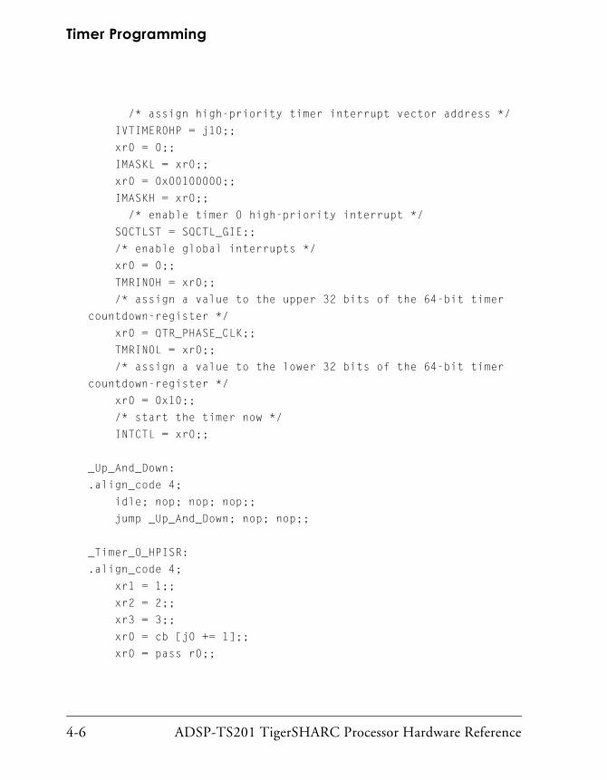
Timer Programming
4-6 ADSP-TS201 TigerSHARC Processor Hardware Reference
/* assign high-priority timer interrupt vector address */
IVTIMER0HP = j10;;
xr0 = 0;;
IMASKL = xr0;;
xr0 = 0x00100000;;
IMASKH = xr0;;
/* enable timer 0 high-priority interrupt */
SQCTLST = SQCTL_GIE;;
/* enable global interrupts */
xr0 = 0;;
TMRIN0H = xr0;;
/* assign a value to the upper 32 bits of the 64-bit timer
countdown-register */
xr0 = QTR_PHASE_CLK;;
TMRIN0L = xr0;;
/* assign a value to the lower 32 bits of the 64-bit timer
countdown-register */
xr0 = 0x10;;
/* start the timer now */
INTCTL = xr0;;
_Up_And_Down:
.align_code 4;
idle; nop; nop; nop;;
jump _Up_And_Down; nop; nop;;
_Timer_0_HPISR:
.align_code 4;
xr1 = 1;;
xr2 = 2;;
xr3 = 3;;
xr0 = cb [j0 += 1];;
xr0 = pass r0;;

ADSP-TS201 TigerSHARC Processor Hardware Reference 4-7
Timers
.align_code 4;
if xaeq, jump _Set_Clock_High_Phase_0; nop; nop; nop;;
/* if at clock phase 0, set the clock high */
xr4 = r0 - r1; nop; nop;;
if xaeq, jump _Set_Clock_High_Phase_1; nop; nop; nop;;
/* if at clock phase 1, set the clock high */
xr4 = r0 - r2; nop; nop;;
if xaeq, jump _Set_Clock_Low_Phase_2; nop; nop; nop;;
/* if at clock phase 2, set the clock low */
xr4 = r0 - r3; nop; nop;;
if xaeq, jump _Set_Clock_Low_Phase_3; nop; nop; nop;;
/* if at clock phase 3, set the clock low */
_Set_Clock_High_Phase_0:
.align_code 4;
xr0 = FLAGREG_FLAG1_OUT; nop; nop; nop;;
FLAGREGST = xr0; nop; nop; nop;;
rti (abs); nop; nop; nop;;
_Set_Clock_High_Phase_1:
.align_code 4;
xr0 = FLAGREG_FLAG1_OUT; nop; nop; nop;;
FLAGREGST = xr0; nop; nop; nop;;
rti (abs); nop; nop; nop;;
_Set_Clock_Low_Phase_2:
.align_code 4;
xr0 = ~(FLAGREG_FLAG1_OUT); nop; nop; nop;;
FLAGREGCL = xr0; nop; nop; nop;;
rti (abs); nop; nop; nop;;

Timer Expired (TMR0E) Pin and Signal Timing
4-8 ADSP-TS201 TigerSHARC Processor Hardware Reference
_Set_Clock_Low_Phase_3:
.align_code 4;
xr0 = ~(FLAGREG_FLAG1_OUT); nop; nop; nop;;
FLAGREGCL = xr0; nop; nop; nop;;
rti (abs); nop; nop; nop;;
_main.end:
Timer Expired (TMR0E) Pin and Signal Timing
The timer 0 expired (TMR0E) pin indicates that timer 0 has expired. When this timer expires, the processor issues a high pulse on the TMR0E pin for four SCLK cycles. It is important to note (as shown in Figure 4-1 on page 4-2) that the timer is a bus slave on the SOC bus. Because processor core accesses to control the timer must cross clock domains, the response of the timer may be affected by SOC interface loading. For more information on clock domains, see “SOC Interface” on page 3-1. For more information on TMR0E pin timing, see the ADSP-TS201 TigerSHARC Embedded Pro-cessor Data Sheet.

ADSP-TS201 TigerSHARC Processor Hardware Reference 5-1
5 FLAGS
The TigerSHARC processor has four general-purpose input or output flag (FLAG3–0) pins. Each pin may be configured as an input or output. As out-puts, programs may use the flag pins to signal events or conditions to any external device such as a host processor. As inputs, programs may read the flag pin input state in the FLAGREG register or use the pin input state as a condition in conditional instructions. After powerup reset, the FLAG3–0 pins are inputs with internal pull-up resistors that hold them at logic high value.
Flag OperationsTo setup and use input and output flag pins, use the following procedure:
1. Use the FLAGx_EN bits in the FLAGREG register to configure each of the FLAG3–0 pins as an input (FLAGx_EN=0) or output (FLAGx_EN=1).
2. (for output flag pins) Use the FLAGx_OUT bits in the FLAGREG regis-ter to select the output value for each of the FLAG3–0 pins.
3. (for input flag pins) Read the FLGx bits in the SQSTAT register to view the input value for each of the FLAG3–0 pins, or use the input flag conditions (FLAGx_IN) in conditional instructions.
As shown in Figure 5-1, the flag unit is a bus slave on the SOC bus. It is important to note that input and output flag operations must cross a num-ber of clock domains when changing output values or responding to

Flag Operations
5-2 ADSP-TS201 TigerSHARC Processor Hardware Reference
input. To guarantee that flag I/O is not lost, use a handshake protocol for flag I/O in the system. For more information on clock domains, see “SOC Interface” on page 3-1.
Figure 5-1. Flags and SOC Bus Connections
S-Bus
Memory
I-Bus
K-Bus
J-Bus
Processor CoreCompute Blocks
Integer ALUsSequencer
Non-Ureg Registers
SOCInterface
LinkPorts
ExternalPort (EBIU)
JTAGPort DMA
Timer
Interrupts
SOCBus
Flags
ClusterBus
128 Bits WideOperates at SOCCLK rate
Each128 Bits
WideOperateat CCLK
rate
64 Bits WideOperates atSCLK rate
Operate atLxCLKIN/OUT
rate
Extended CoreOperates atCCLK rate
Operate atSCLK rateOperates at
TCK rate
Interrupt Vector
FLAGx TMR0E DMARxIRQx

ADSP-TS201 TigerSHARC Processor Hardware Reference 5-3
Flags
Flag ProgrammingThe examples in Listing 5-1, Listing 5-2, Listing 5-3, and Listing 5-4 pro-vide a programming example for flag setup and usage. It is useful to observe the operation of this code on an EZ-Kit Lite demonstration sys-tem, noting the operation of timers, interrupts, and flags.
Listing 5-1. Loop Generating Flag Output(EZ-Kit Blink Example in Assembly)
/* This TigerSHARC assembly program toggles flag pin outputs to
blink connected LEDs on the ADSP-TS201 EZ-Kit. */
/* Macro definitions and include statements */
#include <defTS201.h>
/* Program Code for internal memory block 0 */
.section program;
/* Flag setup */
flagregst = FLAGREG_FLAG2_EN | FLAGREG_FLAG3_EN |
FLAGREG_FLAG2_OUT | FLAGREG_FLAG3_OUT ;;
/* FLAG2 and FLAG3 output enable */
flagregcl = ~(FLAGREG_FLAG2_OUT);;
_done:
lc0 = 0x989680;; /* this count sets a quick toggle speed */
/* lc0 = 0x5F5E10;; */ /* count for very quick toggle speed */
/* lc0 = 0x2FAF080;; */ /* count for slow toggle speed */
.align_code 4;

Flag Programming
5-4 ADSP-TS201 TigerSHARC Processor Hardware Reference
_loop1:
if nlc0e, jump _loop1 (NP); nop;nop;nop;;
xR0 = FLAGREG;;
/* flag toggle to blink EZ-Kit LEDs */
xR1= FLAGREG_FLAG2_OUT | FLAGREG_FLAG3_OUT;;
/* toggle flags */
xR0 = R0 XOR R1;;
FLAGREG = xR0;;
.align_code 4;
jump _done;nop;nop;nop;;

ADSP-TS201 TigerSHARC Processor Hardware Reference 5-5
Flags
Listing 5-2. Flag Input Generating Flag Output(EZ-Kit Push Buttons to LEDs Example)
/* This TigerSHARC assembly program uses flag input (pushbuttons)
to toggle flag pin outputs to blink connected LEDs on the
ADSP-TS201 EZ-Kit. */
// Macro Definitions & Includes
#include <defTS201.h>
.section program;
_start:
xR0 = 0x00000000;;
FLAGREG = xR0;;
/* clear all flag settings */
flagregst = FLAGREG_FLAG2_EN | FLAGREG_FLAG3_EN;;
/* enable FLAG2, FLAG3 as outputs */
j0 = _IRQ0_ISR;;
/* set IVIRQ0 interrupt vector */
IVIRQ0 = j0;;
xR0 = INT_IRQ0;;
/* unmask IRQ0 interrupt */
IMASKH = xR0;;
/* Write contents back to IMASKH register */
xr0 = SQCTL;;
/* Read contents of SQCTL register */
xr0 = bset r0 by SQCTL_GIE_P;;
/* Unmask and global interrupts enable */

Flag Programming
5-6 ADSP-TS201 TigerSHARC Processor Hardware Reference
SQCTL = xR0;;
/* Write contents back to IMASKH register */
_testflag0:
xR0 = SQSTAT;;
/* check FLAG0 status */
bitest r0 by 16;;
if xSEQ, jump _turnoff_flag2 (NP);;
_turnon_flag2:
flagregst = FLAGREG_FLAG2_OUT;;
/* turn on LED/FLAG2 */
jump _testflag1 (NP);;
_turnoff_flag2:
flagregcl = ~(FLAGREG_FLAG2_OUT);;
/* turn off LED\FLAG2 */
_testflag1:
xR0 = SQSTAT;;
/* check FLAG1 status */
bitest r0 by 17;;
if xSEQ, jump _turnoff_flag3 (NP);;
_turnon_flag3:
flagregst = FLAGREG_FLAG3_OUT;;
/* turn on LED/FLAG3 */
jump _delayloop (NP);;
_turnoff_flag3:
flagregcl = ~(FLAGREG_FLAG3_OUT);;
/* turn off LED/FLAG3 */

ADSP-TS201 TigerSHARC Processor Hardware Reference 5-7
Flags
_delayloop:
/* delay loop */
LC0 = 0x400000;;
.align_code 4;
wait0:
if NLC0E, jump wait0 (NP);;nop;;nop;;nop;;
jump _testflag0 (NP);;
_IRQ0_ISR:
/* IRQ0 ISR */
/* An RTI cannot be the first instruction of an ISR */
xr0 = FLAGREG;; /* check FLAG2/3 status */
xr0 = btgl r0 by FLAGREG_FLAG2_OUT_P;; /* toggle FLAG2 */
xr0 = btgl r0 by FLAGREG_FLAG3_OUT_P;; /* toggle FLAG3 */
FLAGREG = xr0;; /* write it back */
LC1 = 0x400000;; /* delay loop */
.align_code 4;
wait1:
if NLC1E, jump wait1 (NP);;nop;;nop;;nop;;
xr0 = FLAGREG;; /* check FLAG2/3 status */
xr0 = btgl r0 by FLAGREG_FLAG2_OUT_P;; /* toggle FLAG2 */
xr0 = btgl r0 by FLAGREG_FLAG3_OUT_P;; /* toggle FLAG3 */
FLAGREG = xr0;; /* write it back */
LC1 = 0x400000;; /* delay loop */
.align_code 4;
wait2:
if NLC1E, jump wait2 (NP);;nop;;nop;;nop;;
rti (NP) (ABS);;

Flag Programming
5-8 ADSP-TS201 TigerSHARC Processor Hardware Reference
Listing 5-3. Loop Generating Flag Output (EZ-Kit Flag Test Example)
/* This C program toggles flag pin outputs to blink connected
LEDs on the ADSP-TS201 EZ-Kit. */
#include “flag.h”
#include <sysreg.h>
#include <builtins.h>
volatile int i, j;
void main()
InitFlagAsOutput(2); /* Assign FLAG2 as an output */
InitFlagAsOutput(3); /* Assign FLAG3 as an output */
FlagHigh(2); /* Set FLAG2 high */
FlagLow(3); /* Set FLAG3 low */
while(1) /* Setup infinite loop here... */
for(i=0; i<8000000; i++);
/* Add an arbitrary delay here */
FlagLow(2); /* Set FLAG2 low */
FlagHigh(3); /* Set FLAG3 high */
for(j=0; j<8000000; j++);
/* Add an arbitrary delay here */
FlagHigh(2); /* Set FLAG2 high */
FlagLow(3); /* Set FLAG3 low */
/* End infinite WHILE(1) loop... */
/* End of main()... */

ADSP-TS201 TigerSHARC Processor Hardware Reference 5-9
Flags
Listing 5-4. Loop Generating Flag Output(EZ-Kit Blink Example in C)
/* This C program sets up a periodic timer interrupt to generate
flag output. On the ADSP-TS201 EZ-Kit, this program lights up
LEDs for each flag output. */
#include <defts201.h>
#include <sysreg.h>
#include <signal.h>
#define SET_INTCTL(x) asm(“INTCTL=%0;;”::”y”(x))
#define SET_FLAG(x) asm(“FLAGREGST=%0;;”::”y”(x))
#define CLR_FLAG(x) asm(“FLAGREGCL=%0;;”::”y”(x))
#define TIMER1H_PERIOD 25000000/2
volatile int irq0_count = 0;
volatile int irq1_count = 0;
volatile int blink_speed = 0;
volatile int timer_count = 0;
void irq1_isr(int signal)
irq1_count++;
// while(1);
if (irq1_count&1)
SET_FLAG(FLAGREG_FLAG1_OUT);
else
CLR_FLAG(~FLAGREG_FLAG1_OUT);
/* end irq1_isr */
void irq0_isr(int signal)
irq0_count++;
blink_speed--;

Flag (FLAG3-0) Pin and Signal Timing
5-10 ADSP-TS201 TigerSHARC Processor Hardware Reference
if (blink_speed<0)
blink_speed = 2;
/* end irq0_isr */
void timer1h_isr(int signal)
timer_count++;
if ((timer_count>>blink_speed)&1)
SET_FLAG(FLAGREG_FLAG0_OUT);
else
CLR_FLAG(~FLAGREG_FLAG0_OUT);
/* end timer1h_isr */
void main(void)
__builtin_sysreg_write(__IMASKH, 0);
__builtin_sysreg_write(__IMASKL, 0);
__builtin_sysreg_write(__TMRIN1H, 0);
__builtin_sysreg_write(__TMRIN1L, TIMER1H_PERIOD);
SET_FLAG(FLAGREG_FLAG0_EN|FLAGREG_FLAG1_EN);
interrupt(SIGIRQ0, irq0_isr);
interrupt(SIGIRQ1, irq1_isr);
interrupt(SIGTIMER1HP, timer1h_isr);
SET_INTCTL(INTCTL_TMR1RN);
while(1);
/* end main */
Flag (FLAG3-0) Pin and Signal TimingThe flag input and/or output (FLAG3–0) pins let the processor signal exter-nal devices or receive input from them. It is important to note (as shown in Figure 5-1 on page 5-2) that the flag unit is a bus slave on the SOC bus. Because processor core accesses to control the flag unit must cross clock domains, the response of the flags may be affected by SOC interface load-
ADSP-TS201 TigerSHARC Processor Hardware Reference 5-11
Flags
ing. For more information on clock domains, see “SOC Interface” on page 3-1. For more information on FLAG3–0 pin timing, see the ADSP-TS201 TigerSHARC Embedded Processor Data Sheet.

Flag (FLAG3-0) Pin and Signal Timing
5-12 ADSP-TS201 TigerSHARC Processor Hardware Reference

ADSP-TS201 TigerSHARC Processor Hardware Reference 6-1
6 INTERRUPTS
The TigerSHARC processor supports a variety of interrupts—external or internal event indicators. Interrupts can serve any of the following pur-poses in a system.
• Synchronization between core and non-core operations
• Error detection
• Debug feature operations
• Controls introduced by an application
Interrupts on the TigerSHARC processor are classified as either software interrupts or hardware interrupts.
Most interrupts in the TigerSHARC processor are dedicated. Four inter-rupt pins and two interrupt registers support general-purpose interrupts. All interrupt sources other than the interrupt pins and interrupt register are caused by events or dedicated hardware. For each interrupt there is a vector register in the Interrupt Vector Table (IVT) (in register groups 0x38 and 0x39) and a bit number in the interrupt latch, mask, and prior-ity mask registers.
For performance considerations, when a hardware interrupt occurs, it does not break the pipeline. The first instruction of the interrupt routine is inserted into the instruction flow after it has occurred. From this point, the instructions that are already in the pipeline complete their execution.

6-2 ADSP-TS201 TigerSHARC Processor Hardware Reference
Software interrupts are caused by an instruction that causes an internal event. Other instructions left in the instruction pipeline are not completed (flushed) after the instruction that has caused the software interrupt.
Hardware interrupts are caused by input to the external interrupt (IRQ3–0) pins and timer interrupts. Instructions left in the instruction pipeline are not completed after the cycle that the external interrupt is recognized. Hardware error interrupts are caused by:
• DMA error
• Inactive AutoDMA access
• Self multiprocessor space read
• Link port error
• Broadcast read from external memory
For more information on the instruction pipeline and interaction with interrupts, see Chapter 8, “Program Sequencer” in the ADSP-TS201 TigerSHARC Processor Programming Reference.
Interrupts are either level-sensitive or edge-sensitive—the hardware inter-rupts (IRQ3–0) can be configured as either level- or edge-sensitive according to the programming in the INTCTL register. The differences between the two types of interrupts are:
• Edge-sensitive interrupts are latched when they occur and remain latched until serviced or reset by an instruction. If it is not cleared during servicing, no new event is identified and the continued request is ignored.
• Level-sensitive interrupt requests must be sustained until serviced, otherwise they are not seen. If the request continues after being ser-viced, it is considered a new interrupt.

ADSP-TS201 TigerSHARC Processor Hardware Reference 6-3
Interrupts
A level-sensitive interrupt is normally driven as a result of some accessible register state and cleared either by reading the register or by writing an inactive value into it.
An edge-sensitive interrupt is event triggered (for example, by expiration of a timer).
The edge- or level-sensitivity for each interrupt is listed in “Interrupt Vector Table” on page 6-17.
Each of the interrupts implemented in the TigerSHARC processor has an interrupt vector register, which is the address of the interrupt routine that services the appropriate interrupt. The whole register file (31 entries with another 32 reserved entries) is referred to as the Interrupt Vector Table (IVT). The registers are 32 bits each, in order to enable internal and exter-nal memory interrupt routines.
For boot procedures, some of the interrupt vector registers are initialized at reset to specific addresses. In boot by EPROM and boot by link opera-tions, a DMA is initialized to load the boot data into memory address 0x0. When the boot DMA is executed, it issues a DMA interrupt. The DMA interrupt vector is also initialized to address 0x0.
To issue an interrupt, an interrupt request pin, IRQ3-0, is asserted. Each of the IRQ3-0 pins may be individually set to either edge-triggered or level-sensitive. See “Interrupt Control (INTCTL) Register” on page 2-45.
Software interrupts that are caused by a specific instruction occur immediately after the instruction that caused them. Therefore the pipeline is flushed after a software interrupt, and the instructions that were in the pipeline are not executed.
As shown in Figure 6-1, the interrupt unit is a bus slave on the SOC bus. It is important to note that interrupt register accesses must cross a number of clock domains when reading or writing register data. Corresponding response for software interrupts may vary with SOC bus loading. Because the interrupt vector input from the interrupt unit has a direct connection

6-4 ADSP-TS201 TigerSHARC Processor Hardware Reference
to the program sequencer, response to latched interrupts is not affected by SOC bus loading. For more information on clock domains, see “SOC Interface” on page 3-1.
Figure 6-1. Interrupts and SOC Bus Connections
S-Bus
Memory
I-Bus
K-Bus
J-Bus
Processor CoreCompute Blocks
Integer ALUsSequencer
Non-Ureg Registers
SOCInterface
LinkPorts
ExternalPort (EBIU)
JTAGPort DMA
Timer
Interrupts
SOCBus
Flags
ClusterBus
128 Bits WideOperates at SOCCLK rate
Each128 Bits
WideOperateat CCLK
rate
64 Bits WideOperates atSCLK rate
Operate atLxCLKIN/OUT
rate
Extended CoreOperates atCCLK rate
Operate atSCLK rate
Operates atTCK rate
Interrupt Vector

ADSP-TS201 TigerSHARC Processor Hardware Reference 6-5
Interrupts
Interrupt OperationsInterrupt operations on the processor include interrupt setup, interrupt (or exception) handling, and returning from the interrupt. The interrupt controller includes the following interrupt setup and control registers:
• Interrupt control (INTCTL) register
• Interrupt mask (IMASK) registers – IMASKH and IMASKL
• Priority mask (PMASK) registers – PMASKH and PMASKL
• Interrupt latch (ILAT) registers – ILATH and ILATL
The IMASK, PMASK, and ILAT registers have identical bit definitions; one bit for each interrupt source. The definitions for these registers are available in Figure 2-14 on page 2-48, Figure 2-15 on page 2-48, Figure 2-16 on page 2-49, Figure 2-17 on page 2-49, and Figure 2-13 on page 2-45. Additional programming information on these registers is available in Chapter 8, “Program Sequencer” in the ADSP-TS201 TigerSHARC Proces-sor Programming Reference.
INTCTL Register
The INTCTL register is a 32-bit register that controls interrupt pin sensitiv-ity (level- or edge-sensitive interrupts). This register also provides run/stop control for the timers.
IMASK Register
The IMASK register is a single 64-bit register accessed as two 32-bit regis-ters, IMASKL and IMASKH. Mask bits are individually dedicated to different interrupts. When an interrupt bit is set in the ILAT register, the corre-sponding interrupt is only accepted if the corresponding bit is also set in the IMASK register. Consequently, the order of the interrupt bits is identi-

Interrupt Operations
6-6 ADSP-TS201 TigerSHARC Processor Hardware Reference
cal to those found in the ILAT register. Bit2 in the SQCTL register is a global interrupt enable (GIE) bit. When cleared, no interrupts, except for excep-tion and emulation, are enabled.
PMASK Register
The PMASK register is a single 64-bit register that is accessed as two 32-bit registers, PMASKL and PMASKH. This register is identical to the IMASK register in bit assignment.
These registers help the hardware track nested interrupts by masking all interrupts with a lower or equal priority than the interrupt that is cur-rently being executed. The PMASK is a 64-bit register, of which 32 bits are implemented and 32 are reserved. When the TigerSHARC processor begins to service an interrupt, its bit in PMASK is set. Each set bit indicates this ISR is active or nested at some level. The most significant set bit in PMASK indicates which interrupt is currently served. The current interrupt bit is cleared once the service is completed, either by RTI instruction or by RDS instruction (see “if cond, RTI (ABS)” and “if cond, RDS” in the ADSP-TS201 TigerSHARC Processor Programming Reference).
When the PMASK is nonzero, all the interrupts with a lower or equal prior-ity to the most significant set bit in PMASK are disabled by it. For logic equations, the PMASK_R is defined as the mask created by PMASK; that is, all the bits above the most significant set bit are set and other bits are clear. A PMASK_R is only a definition and not a register.
The RETI register is updated only in the Execute2 pipe stage of the first instruction of the interrupt service routine. The first instruction cannot be an instruction that uses its value, such as RTI or RETI.

ADSP-TS201 TigerSHARC Processor Hardware Reference 6-7
Interrupts
During normal operations the PMASK is zero, and PMASK_R is 0xFF…F.
1. Assume that a link #0 interrupt occurred. PMASK = 0x00…040, and PMASK_R = 0xFF…F80. The interrupts of lower priority than link #0—namely, timer low priority interrupts and link #0 interrupt—are disabled by PMASK.
2. Following this, assume a DMA #2 interrupt occurred. PMASK = 0x00….08040, and PMASK_R is 0xFF…F0000. The timer low prior-ity, link, and DMA #0, #1 and #2 interrupts are disabled by PMASK. Returning from interrupt (which is DMA #2 interrupt) clears the most significant set bit in PMASK which is bit #15. The PMASK regis-ter is now 0x00…040, and PMASK_R is 0xFF…F80. The timer low priority interrupts and link #0 interrupt are disabled by PMASK, but the other link interrupts and DMA interrupts are enabled again.
ILAT Register
The ILAT register is a single 64-bit register accessed as two 32-bit registers, ILATL and ILATH. Each bit is dedicated to an interrupt—when an interrupt occurs and is latched, the corresponding bit is set. The order of interrupt bits is the interrupt priority—Bit0 is the lowest priority. See “Interrupt Mask (IMASKL/IMASKH) Registers” on page 2-47 for bit assignments.
An application may emulate an interrupt by writing to the ILAT register set address (ILATSTL or ILATSTH). Writing to these addresses updates the ILAT register to the OR of the old value and the new written value. As a result, every set bit in the written data sets the corresponding bit in the ILAT register. Setting an interrupt bit causes the TigerSHARC processor to assume the corresponding interrupt has occurred.
Interrupt bits can also be cleared by writing to the clear addresses (ILATCLL or ILATCLH). Such a write ANDs the data written with the old data of the ILAT register. In this case, a zero bit in the input data clears the corre-sponding bit in ILAT, while a set bit keeps it unchanged. This way, an

Interrupt Operations
6-8 ADSP-TS201 TigerSHARC Processor Hardware Reference
application can clear a pending interrupt before it is executed. Such an operation is very sensitive, and it should be executed under these conditions:
• Non-implemented (reserved) bits may not be set. When writing to either set or clear address, the reserved bits must be zero.
• Exception and emulation exception bits may not be set through ILATST. In order to cause an exception, use a TRAP instruction; in order to cause an emulation exception, use an EMUTRAP instruction.
• Interrupts that are level-triggered should not be changed—link interrupts, hardware error interrupts, or IRQ bits if programmed to be level-triggered.
• Writes to ILATL or ILATH should not be attempted.
• An interrupt should be cleared while it is masked, otherwise it may be served before it is cleared.
• Like all other sequencer registers, the set and clear addresses are single-word writes only.
Interrupt Service RoutinesWhen an interrupt occurs, the corresponding bit in the ILAT register is set. The ILAT bits are ANDed with the enable bits in the IMASK and with PMASK_R. If the global interrupt enable (GIE) bit in the SQCTL register is set and the result of the ILAT and IMASK and PMASK_R is not zero, the highest priority interrupt that is enabled is served.
ADSP-TS201 TigerSHARC Processor Hardware Reference 6-9
Interrupts
All the level-sensitive interrupts (IRQ3–0 pin interrupts, link port inter-rupt, and hardware error interrupt) may be deasserted only in one of the following states:
• During the interrupt service routine of this specific interrupt
• While the specific interrupt is disabled
• While all hardware interrupts are disabled
The following algorithm describes the interrupt service routine (ISR).
1. The interrupt vector in Interrupt Vector Table (IVT) is used as the next fetch address and the ISR’s first instruction is pushed into the pipeline.
If the interrupt is a hardware interrupt, normal execution contin-ues until the first instruction of the interrupt routine reaches pipeline stage EX2. Otherwise, for software exceptions that are not hardware interrupts, all the normal flow instructions that are in the pipeline are aborted.
While an interrupt is in the pipeline, all the hardware interrupts are disabled, although this is not reflected in the mask registers (PMASK or IMASK).
If the exception is disabled, the ILAT bit for the exception is not set and the exception is ignored. The reason is that the instruction line that caused the exception is lost.
In an ISR, the first instruction must not be RDS or RTI.
2. Instructions in the pipeline are executed.
3. Before the first instruction in the interrupt routine reaches pipeline stage EX2, the global interrupt enable (GIE) is rechecked. If the bit was cleared since the interrupt was generated by an instruction

Interrupt Operations
6-10 ADSP-TS201 TigerSHARC Processor Hardware Reference
already in the pipeline, then all the instructions in the pipeline are aborted and the TigerSHARC processor begins fetching from the normal flow (as if there were no interrupt).
If instructions are ordered in a specific way, it is possible to enter an ISR immediately after its bit is cleared in the IMASK register. While in the ISR, IMASK bit = 0, which does not affect operation in any way.
4. The return PC (which points to the instruction that would have been executed had the interrupt not occurred) is saved in the appropriate register—RETI for a hardware interrupt, RETS for a software interrupt, or DBGE for an emulation debug.
5. The TigerSHARC processor mode is changed to emulation mode if there was an emulation exception; otherwise it changes to supervi-sor mode.
6. When the first instruction in the interrupt routine reaches pipeline stage EX2 and if the interrupt is edge-triggered, the corresponding interrupt bit in the ILAT register is reset, and the same bit in the PMASK register is set. The interrupt bit in PMASK is set in any case, not just when the interrupt is level-sensitive.
A software interrupt occurs only when the instruction that caused it reaches pipeline stage EX2. When a software interrupt that was enabled occurs, all the instructions in the pipeline after the instruction that caused the exception are aborted, including hardware interrupt routine instruc-tions. If a software interrupt occurs during the time that the hardware interrupt is in the pipeline, the hardware interrupt is aborted with other instructions in the pipeline and the software interrupt procedure begins. The hardware interrupt bit is not reset, however, in order to save the (hardware) interrupt.

ADSP-TS201 TigerSHARC Processor Hardware Reference 6-11
Interrupts
The hardware ISR steps, illustrated and numbered in Figure 6-2, are as follows.
1. The processor determines the state after hardware interrupt (GIE AND IMASKN AND PMASK_RN).
2. The processor (after determining that masks are set):
a. Inserts the ISR fetch address
b. Stores the PC in RETI when the instruction reaches pipeline stage EX2
Storing PC in RETI happens only after the first instruction of the interrupt routine reaches EX2 with ILAT clear and PMASK bits set, if step 4 (below) conditions are met.
c. Executes instructions in pipeline, unless it encounters an exception or emulation condition
Note that exceptions and emulation conditions are not affected by GIE set.
3. The processor checks whether GIE is set when the first instruction in the ISR reaches pipeline stage EX2.
a. If NO, the processor flushes the pipeline, aborts the inter-rupt, and waits for next instruction.
b. If YES, the processor clears ILATN if interrupt is edge triggered
Note that exceptions and emulation conditions are not affected by GIE set.

Interrupt Operations
6-12 ADSP-TS201 TigerSHARC Processor Hardware Reference
Figure 6-2. Hardware Interrupts
NO
NO
YES
YES
NO
YES
ENABLED
GIEAND IMASK[N]AND PMASK_R[N]
FLUSH PIPEABORT INTERRUPT
INSERT ISR FETCH ADDRESSSTORE PC IN RETIEXECUTE INSTRUCTIONS IN PIPE
HW INTERRUPTILAT[N] SET
ISR@EX2
IS GIE SET?
ILAT[N] CLEAREDPMASK[N] SET
IF NESTING:STORE CONTEXTSTORE RETIB: EXECUTE ISR
RESTORE RETIB:RESTORE CONTEXTRTI
PMASK[N] CLEAREDJUMP TO RETI
1
2
3
3B
4
7
6
5
USER
SYSTEM
SYSTEMSYSTEM
SYSTEM
SYSTEM
SYSTEM
SYSTEM
USER
USER
3A

ADSP-TS201 TigerSHARC Processor Hardware Reference 6-13
Interrupts
4. If nesting, for hardware interrupt, the ISR should start by storing the processor context and store the contents of RETIB.
Note that instructions for storing the processor context and RETIB must be specified in the ISR.
5. The ISR executes, servicing the interrupt.
6. If the nesting was enabled, the ISR should end by restoring the RETIB contents, restoring the processor context and executing an RTI instruction.
Note that the instructions for restoring RETIB and the processor context must be specified in the ISR.
7. After the ISR completes, the processor clears PMASKN and jumps to RETI address.
Handling Interrupts
There are two methods of interrupt handling: one that uses nesting and one that does not. If the interrupt handling does not use nesting, other interrupts are disabled throughout the ISR or handling routine. If the interrupt handling routine does enable nesting, some special programming is required. The special programming required for nested interrupt han-dling routines is described in this section.
The first instructions in the interrupt routine must be dedicated to pre-serving the current status of the machine. All the registers used by the interrupt routine must be pushed onto a stack. The TigerSHARC proces-sor does not require a dedicated stack pointer since any one of the IALU registers can be used as a stack pointer. The application can store and load registers with the post-modify option, and it can work with two stacks in two memory blocks and store eight words every cycle.

Interrupt Operations
6-14 ADSP-TS201 TigerSHARC Processor Hardware Reference
While preserving the current machine status in a stack, the appropriate global interrupt enable bit (hardware or software) is still clear, so there is no danger of corrupting the return address PC (RETI). If, however, the interrupt was a hardware interrupt, software or emulation exceptions can still be processed, since the return address is saved in a different register (RETS or DBGE). This also applies to emulation exceptions when a software interrupt is executing its initial cycles.
Once the relevant registers are saved in memory, the return register should be saved. This operation is performed automatically by saving the return address alias RETIB. The RETIB register is an aliased name for RETI. If you use RETIB, you access RETI. Note that interrupt nesting is enabled by sav-ing off RETIB to memory or to another register.
If the system does not need to support nested hardware interrupts, there is no need to preserve the machine state in a stack. The return can be exe-cuted from the RETI register, and the hardware interrupt’s global disable bit should be left as is. However, software interrupts or debug interrupts may be nested. In these cases, the machine state should be retained before software/debug service is performed.
Returning From an Interrupt
The return from interrupt is performed using the RTI instruction (see “if cond, RTI (ABS)” in the ADSP-TS201 TigerSHARC Processor Program-ming Reference). The return address should be put in the RETIB register (recommended at about eight cycles beforehand to enable BTB usage). In non-nested hardware interrupt routines, the return address is already in the RETI register. If the non-nested exception is taken, the return address should be copied from the RETS or DBGE register (according to exception type) to the RETI register before the return. The use of the RETIB alias dis-ables all interrupts until the RTI instruction is executed—this is to protect the RETI register from being destroyed by another interrupt occurrence.

ADSP-TS201 TigerSHARC Processor Hardware Reference 6-15
Interrupts
The state of the machine must be saved in memory at the beginning of the interrupt routine. The full state should be restored in the original registers before the return. See “Handling Interrupts” on page 6-13.
The RTI instruction clears the highest set bit in PMASK register. The instruction then jumps to the address pointed by the value in the RETI reg-ister and re-enables the interrupts.
Interrupt routine restrictions:
• An interrupt routine may not refer to the RETI or RETS registers on the first instruction line.
• An interrupt routine may not use the RTI, RETI, or RDS instructions on the first instruction line.
Handling Exceptions
Exceptions are software interrupts—interrupts that are caused by code being executed. Figure 6-3 illustrates what transpires when a software interrupt is introduced. If the exception is enabled:
• SQCTL[21] is set in case of a regular exception, or SQCTL[22] is set in case of an emulation exception.
• The sequencer starts fetching from the address pointed to by the IVSW register in case of an exception, or from the EMUIR register in case of an emulation exception.
• PC is stored in RETS in case of an exception, or in DBGE register in case of an emulation exception.
• Instructions are flushed from the pipeline.
The return is executed by transferring the return address from RETS or DBGE (or from where it has been stored) to RETI without using RETIB. Then the RTI instruction should be executed.

Interrupt Operations
6-16 ADSP-TS201 TigerSHARC Processor Hardware Reference
If an exception occurs when it is not enabled, the exception is cleared and not serviced.
The exceptions are treated differently from other interrupts:
• The exception is tied to the instruction that caused it. The excep-tion process begins when the instruction that caused the exception reaches pipeline stage EX2. When this occurs, all instructions in the pipeline are aborted. If the instruction that caused the excep-
Figure 6-3. Software Exception (Interrupt)
NO
YES
ILAT[62] SET
STORE RETS IN MEMORYSTORE RETIEXECUTE ISRSAVE RETSFROM MEMORY TO RETIRTI; RESTORE RETI
EXCEPTIONCLEARED
EXCEPTIONOCCURS
ENABLED?
SQCTL[5] SET]
INSERT ISR FETCH ADDRESSSTORE PC IN RETSFLUSH INSTRUCTIONS IN PIPE
JUMP TO RETI
ISR@EX2

ADSP-TS201 TigerSHARC Processor Hardware Reference 6-17
Interrupts
tion was speculative and it was aborted, the exception does not take place. Unlike an abort, a predicated instruction that is not executed due to the condition can still cause the exception.
• The return address is saved in a different register to enable nesting between the hardware interrupt and the exception. The registers are RETS for exception or DBGE for emulation trap.
• If the exception is disabled when it is occurring, it is not latched. It is not latched because it is irrelevant to do so without the return address pointing to the cause (RETS or DBGS registers). In these cases the exception is lost.
• In order to protect the old RETI value before returning you must execute the following instruction lines, then jump to RETS:
[j31+temporary address] = RETI;;
RETI = RETS;;
RTI; RETI = [j31+temporary address];;
Interrupt Vector TableThe following subsections describe the interrupt types, noting the corre-sponding interrupt bit in the ILAT and IMASK interrupt registers.
Table 6-1. ADSP-TS201 Interrupt Vector Table
Priority Interrupt Description Sensitivity
63 (highest) DBG Debug exception. See “Emulation Exception Interrupt” on page 6-24.
edge
62 SW Software exception. See “Software Exception Interrupts” on page 6-23.
edge
61–58 Reserved Reserved
57 HWERR Hardware error. See “Hardware Error Interrupt” on page 6-22.
level

Interrupt Operations
6-18 ADSP-TS201 TigerSHARC Processor Hardware Reference
56–54 Reserved Reserved
53 TIMER1H Timer 1 high priority. See “Timer Expired Inter-rupts” on page 6-19.
edge
52 TIMER0H Timer 0 high priority edge
51 Reserved Reserved
50 BUSLOCK Buslock. See “Bus Lock Interrupt Register” on page 6-21.
edge
49 Reserved Reserved
48 VIRPT Vector Interrupt. See “Vector Interrupt” on page 6-21.
edge
47–45 Reserved Reserved
44 IRQ3 IRQ3 pin. See “External (IRQ3–0) Input Inter-rupts” on page 6-20.
edge or level
43 IRQ2 IRQ2 pin edge or level
42 IRQ1 IRQ1 pin edge or level
41 IRQ0 IRQ0 pin edge or level
40–39 Reserved Reserved
38 DMA13 DMA channel 13 complete. See “DMA Com-plete Interrupts” on page 6-20.
edge
37 DMA12 DMA channel 12 complete. edge
36–33 Reserved Reserved
32 DMA11 DMA channel 11 complete edge
31 DMA10 DMA channel 10 complete edge
30 DMA9 DMA channel 9 complete edge
29 DMA8 DMA channel 8 complete edge
28–26 Reserved Reserved
25 DMA7 DMA channel 7 complete edge
24 DMA6 DMA channel 6 complete edge
23 DMA5 DMA channel 5 complete edge
22 DMA4 DMA channel 4 complete edge
Table 6-1. ADSP-TS201 Interrupt Vector Table (Cont’d)
Priority Interrupt Description Sensitivity

ADSP-TS201 TigerSHARC Processor Hardware Reference 6-19
Interrupts
Timer Expired Interrupts
There are four timer interrupts: two for each timer, one as high priority and one as low priority. The purpose of having the two priorities per timer is to enable the user to choose which priority is needed. The timer inter-rupt vector registers are IVTIMER0HP, IVTIMER1HP, IVTIMER0LP, and IVTIMER1LP.
When the timer interrupt occurs, both high and low priority bits are set in ILAT (for example, for Timer 0 both Bit2 and Bit52). This is accom-plished by enabling the appropriate interrupt. When an interrupt bit for a timer (INT_TIMER0LP, INT_TIMER1LP, INT_TIMER0HP, or INT_TIMER1HP) in
21–18 Reserved Reserved
17 DMA3 DMA channel 3 complete edge
16 DMA2 DMA channel 2 complete edge
15 DMA1 DMA channel 1 complete edge
14 DMA0 DMA channel 0 complete edge
13–10 Reserved Reserved
9 LINK3 Link port 3 request. See “Link Port Service Request Interrupts” on page 6-20.
level
8 LINK2 Link port 2 request level
7 LINK1 Link port 1 request level
6 LINK0 Link port 0 request level
5–4 Reserved Reserved
3 TIMER1L Timer 1 low priority. See “Timer Expired Inter-rupts” on page 6-19.
edge
2 TIMER0L Timer 0 low priority edge
1 Reserved Reserved
0 (lowest) KERNEL Kernel edge
Table 6-1. ADSP-TS201 Interrupt Vector Table (Cont’d)
Priority Interrupt Description Sensitivity

Interrupt Operations
6-20 ADSP-TS201 TigerSHARC Processor Hardware Reference
the ILATx register is set or cleared by writing to the ILATSTx or ILATCLx registers, both the low and high priority interrupts for that timer are set or cleared.
After reset, the timer interrupts are disabled, and vectors are not initialized.
Link Port Service Request Interrupts
There are four link port channels that normally work with their dedicated DMA channels. The link port service request vector registers are IVLINK0, IVLINK1, IVLINK2, and IVLINK3. When a data element enters the link port receive buffer and its corresponding DMA channel is not initialized, the link port issues a service request interrupt.
After reset, the link interrupts are disabled, and vectors are not initialized.
DMA Complete Interrupts
There are 14 DMA channels. Each DMA channel can generate a DMA complete interrupt. The vector registers are IVDMA0, IVDMA1, IVDMA2, IVDMA3, IVDMA4, IVDMA5, IVDMA6, IVDMA7, IVDMA8, IVDMA9, IVDMA10, IVDMA11, IVDMA12, and IVDMA13. If the interrupt bit in the DMA’s transfer control block (TCB) is set, the DMA channel generates an interrupt when the channel completes the DMA block transfer.
After reset, the DMA interrupts are enabled and vectors are initialized to zero for boot purposes.
External (IRQ3–0) Input Interrupts
There are four general-purpose interrupt pins that can be programmed to be edge- or level-sensitive. The external interrupt (IRQ3–0) pin vector reg-isters are IVIRQ0, IVIRQ1, IVIRQ2, and IVIRQ3. When one of these interrupt pins is activated, an interrupt is issued (if enabled).

ADSP-TS201 TigerSHARC Processor Hardware Reference 6-21
Interrupts
The interrupt type for the interrupt pins is edge- or level-triggered accord-ing to INTCTL programming. See “Interrupt Control (INTCTL) Register” on page 2-45.
After reset, the IRQ interrupts are disabled, unless IRQEN strap option (on pin BM) is used to allow for “no boot, run from memory” mode. For more information on boot options, see “Processor Booting Methods” on page 11-2. Vectors are initialized for boot purposes.
Vector Interrupt
The vector interrupt is a general-purpose interrupt for another master’s use. Another master, either the host or a TigerSHARC processor, can write an address to this register. The write causes a vector interrupt to occur. The value that is written into the register is the address of the inter-rupt routine. The vector interrupt register is VIRPT.
After reset, the vector interrupt is enabled but the vector is not initialized. This is one of the events that can initiate booting by another master.
Bus Lock Interrupt Register
The bus lock interrupt is issued when the bus lock bit in the SQCTL register is set and the TigerSHARC processor becomes the bus master. The bus lock vector register is IVBUSLK. This interrupt is used to indicate that the TigerSHARC processor has locked the external bus.
After reset, the bus lock interrupt is disabled and vectors are not initialized.

Interrupt Operations
6-22 ADSP-TS201 TigerSHARC Processor Hardware Reference
Hardware Error Interrupt
The hardware error interrupt indicates that one of the following errors has occurred:
• Error in DMA – one of the CHxx fields in DSTAT register is 100 (TCB initialization error). Refer to “DMA Status Register (DSTAT/DSTATC)” on page 7-23.
• Data written to the AutoDMA while the corresponding AutoDMA channel is not initialized. Active while Bit17 of SYSTAT is active. Refer to the register description for “System Status (SYSTAT) Reg-ister” on page 2-77.
• Broadcast read from external memory. Active while Bit16 of SYS-TAT is active. Refer to the register description for “System Status (SYSTAT) Register” on page 2-77.
• Access to SDRAM when it is not enabled. Active while Bit18 of SYSTAT is active. Refer to the register description for “System Status (SYSTAT) Register” on page 2-77.
• Self multiprocessing read – active when Bit19 of SYSTAT is active. Refer to the register description for “System Status (SYSTAT) Reg-ister” on page 2-77.
• Link error – in one of the LSTATx registers in the fields RER or TER indicate an error. Refer to “Link Port Error Detection Mecha-nisms” on page 9-19. For additional information refer to “Link Port Status Registers” on page 9-26.
The hardware error interrupt vector register is IVHW.
After reset, the hardware error interrupt is disabled and vectors are not initialized.

ADSP-TS201 TigerSHARC Processor Hardware Reference 6-23
Interrupts
Software Exception Interrupts
Software exceptions are interrupts stemming from code execution. If an exception occurs when the interrupt is disabled, the exception is lost. The software interrupt vector register is IVSW. Software exceptions include:
• Floating-point invalid, if the IVEN bit in the XSTAT/YSTAT register is set. These exceptions are defined by the IEEE standard.
• Underflow, if the UEN bit in the XSTAT/YSTAT register is set
• Overflow, if the OEN bit in the XSTAT/YSTAT register is set
• Debug exceptions that cause supervisor exceptions:
• TRAP instruction
• Watchpoint match, when programmed to cause an exception
• Illegal operations:
• Undefined instruction (not on all cases)
• Illegal combination of instructions
• External access to an illegal space – multiprocessing broadcast read access by either load/store instruction or by fetch
• Illegal misalignment of load – not DAB accessible due to odd address for long-word; or address that is not quad-aligned for quad-word
• Protection violation – access to a supervisor register in user mode
• Two instructions in the same line with one destination
• More than three results in a single compute instruction line (for example, add and subtract, multiply, shift)
Interrupt Operations
6-24 ADSP-TS201 TigerSHARC Processor Hardware Reference
• Two 32-bit immediate instructions in the same line
• More than one branch in the same aligned quad-word with predic-tion bit set
After reset, the software exception is disabled and vectors are not initialized.
For more information on instruction execution and processor core status reported by the software exception, see the ADSP-TS201 TigerSHARC Processor Programming Reference.
Emulation Exception Interrupt
The emulation debug exception causes the TigerSHARC processor to go into emulation mode. The emulation exception does not have an interrupt vector register. After an emulation exception, the TigerSHARC processor fetches from EMUIR register.
In this mode, instructions are read from the JTAG interface and executed in a single step. Emulation mode can be caused by:
• An EMUTRAP instruction
• A watchpoint match (when programmed to cause an emulation trap)
• A JTAG emulation activation
During and after reset, the emulation trap is enabled.

ADSP-TS201 TigerSHARC Processor Hardware Reference 6-25
Interrupts
Interrupt ProgrammingThe example code in Listing 6-1 initializes the two timers and sets up their interrupts. The lower priority interrupt allows nesting, the higher one does not need to allow nesting. The example code in Listing 6-2 shows software exception interrupt handling.
Listing 6-1. Example Code for Nested Interrupts Using Two Timers
/*****************************/
/* */
/* Example of nested interrupts using two timers */
/* */
/******************************/
#include "defts201.h"
.section data1a;
.align 4;
.var register_store[4]; /* Internal memory used to store regis-
ters within ISR */
.align 4;
.var register_store_2[4]; /* Internal memory used to store regis-
ters within ISR */
.section program;
_Setup_Timer_Interrupt_Vectors:
j0 = j31 + _TIMER0HP_ISR;;
IVTIMER0HP = j0;; /* Set Timer0HP Interrupt Vector */
j0 = j31 + _TIMER1HP_ISR;;
IVTIMER1HP = j0;; /* Set Timer1HP Interrupt Vector */
_Unmask_Timer_Interrupts:

Interrupt Programming
6-26 ADSP-TS201 TigerSHARC Processor Hardware Reference
/* Unmasks Timer0 and Timer1 HP Interrupts without */
/* altering previously masked or unmasked interrupts */
xr0 = IMASKH;;
xr1 = INT_TIMER0H | INT_TIMER1H;;
xr0 = r0 or r1;;
IMASKH = xr0;;
_Enable_Hardware_Interrupts:
/* Enable the Hardware Interrupts Enable bit in SQCTL */
SQCTLST = SQCTL_GIE;;
_Setup_Timer_Registers:
/* Load values into Timer0 and Timer1 registers */
xr0 = 0x0;;
xr1 = 0xf;;
xr2 = 0xa;;
TMRIN0H = xr0;;
TMRIN1H = xr0;;
TMRIN0L = xr1;;
TMRIN1L = xr2;;
EnableFlag_out:
/* Enable FLAG2 and FLAG2 as outputs */
FLAGREGST = FLAGREG_FLAG2_EN | FLAGREG_FLAG3_EN;;
_Enable_Timers:
/* Enable the timers without altering any other */
/* settings in the INTCTL register */
xr0 = INTCTL;;
xr1 = INTCTL_TMR0RN | INTCTL_TMR1RN;;
xr0 = r0 or r1;;
INTCTL = xr0;;
_Done:
/* Endless loop */

ADSP-TS201 TigerSHARC Processor Hardware Reference 6-27
Interrupts
nop;nop;nop;nop;;
jump _Done;nop;nop;nop;;
_TIMER0HP_ISR:
/* Interrupt service routine for Timer0HP Interrupt */
/* This interrupt is the lower of the two being used. */
j0 = j31 + register_store;;
q[j0+=4] = xr3:0;; /* Store registers used in ISR to memory */
xr0 = RETIB;; /* Clears SQSTAT[20] enabling servicing of higher
priority interrupts */
/*********************************/
/* Add main function of ISR here */
/*********************************/
xr1 = FLAGREG;;
xr2 = btgl r1 by FLAGREG_FLAG2_OUT_P;;
FLAGREG = xr2;; /* Toggle flag2 LED on EZ-KIT */
RETIB = xr0;; /* Sets SQSTAT[20] no longer enabling servicing of
higher priority interrupts */
j0 = j31 + register_store;;
xr3:0 = q[j0+=4];; /* Restore registers previously saved to mem-
ory */
RTI(ABS);;
_TIMER1HP_ISR:
/* Interrupt service routine for Timer1HP Interrupt. This inter-
rupt is the highest of the two being used. Therefore there is no
need to enable nesting. */
j0 = j31 + register_store_2;;
q[j0+=4] = xr3:0;; /* Store registers used in ISR to memory */
/*********************************/
/* Add main function of ISR here */

Interrupt Programming
6-28 ADSP-TS201 TigerSHARC Processor Hardware Reference
/*********************************/
xr1 = FLAGREG;;
xr2 = btgl r1 by FLAGREG_FLAG3_OUT_P;;
FLAGREG = xr2;; /* Toggle flag3 LED on EZ-KIT */
j0 = j31 + register_store_2;;
xr3:0 = q[j0+=4];; /* Restore registers previously saved to mem-
ory */
RTI(ABS);;

ADSP-TS201 TigerSHARC Processor Hardware Reference 6-29
Interrupts
Listing 6-2. Example Code for Software Exception Interrupt Handling
/******************************/
/* */
/* Example of Software Exception Interrupt handling */
/* */
/*******************************/
#include "defts201.h"
.section data1a;
.align 4;
.var register_store[4]; /* Internal memory used to store regis-
ters within ISR */
.align 4;
.var register_store_2[5]; /* Internal memory used to store regis-
ters within ISR */
.section program;
_Setup_Timer_Interrupt_Vectors:
j0 = j31 + _TIMER0HP_ISR;;
IVTIMER0HP = j0;; /* Set Timer0HP Interrupt Vector */
j0 = j31 + _SW_ISR;;
IVSW = j0;; /* Set Timer0HP Interrupt Vector */
_Unmask_Timer_Interrupts:
/* Unmasks Timer0 Interrupt without altering previously maksed or
unmasked interrupts */
xr0 = IMASKH;;
xr1 = INT_TIMER0H;;
xr0 = r0 or r1;;
IMASKH = xr0;;
Interrupt Programming
6-30 ADSP-TS201 TigerSHARC Processor Hardware Reference
_Enable_HW_SW_Interrupts:
/* Enable Hardware Interrupts and Software exceptions in SQCTL */
SQCTLST = SQCTL_GIE | SQCTL_SW;;
_Setup_Timer_Registers:
/* Load values into Timer0 and Timer1 registers */
xr0 = 0x0;;
xr1 = 0xffff;;
TMRIN0H = xr0;;
TMRIN0L = xr1;;
_Enable_Flag_Out:
/* Enable FLAG2 and FLAG3 as outputs */
FLAGREGST = FLAGREG_FLAG2_EN | FLAGREG_FLAG3_EN;;
_Enable_Timer:
/* Enable the timer without altering any other settings in the
INTCTL register */
xr0 = INTCTL;;
xr1 = INTCTL_TMR0RN;;
xr0 = r0 or r1;;
INTCTL = xr0;;
_Done:
/* Endless loop */
nop;nop;nop;nop;;
jump _Done;nop;nop;nop;;
_TIMER0HP_ISR:
/* Interrupt service routine for Timer0HP Interrupt */
j0 = j31 + register_store;;
q[j0+=4] = xr3:0;; /* Store registers used in ISR to memory */

ADSP-TS201 TigerSHARC Processor Hardware Reference 6-31
Interrupts
/*********************************/
/* Add main function of ISR here */
/*********************************/
j0 = j0+1;;
q[j0+= 4] = xr3:0;; /* Forces a software exception due to
unaligned quad access */
xr1 = flagreg;;
xr2 = btgl r1 by FLAGREG_FLAG2_OUT_P;;
flagreg = xr2;; /* Toggle Flag2 LED */
j0 = j31 + register_store;;
xr3:0 = q[j0+=4];; /* Restore registers previously saved to mem-
ory */
RTI(ABS);;
_SW_ISR:
/* Interrupt service routine for Software Exceptions. This inter-
rupt is higher than all Hardware interrupts. There is no need to
enable nesting as RETS is used to store return address and not
RETI. */
j0 = j31 + register_store_2;;
q[j0+=4] = xr3:0;; /* Store registers used in ISR to memory */
[j0+=1] = RETI;; /* Stores RETI value for last interrupt */
RETI = RETS;; /* Replace RETI with RETS to return to point
where SW exception occurred and not HW interrupt */
/*********************************/
/* Add main function of ISR here */
/*********************************/
xr1 = flagreg;;
xr2 = btgl r1 by FLAGREG_FLAG3_OUT_P;;
flagreg = xr2;; /* Toggle Flag3 LED */
j0 = j31 + register_store_2;;

Interrupt (IRQ3-0) Pin and Signal Timing
6-32 ADSP-TS201 TigerSHARC Processor Hardware Reference
xr3:0 = q[j0+=4];; /* Restore registers previously saved to mem-
ory */
RTI(ABS); RETI = [j31 +j0];; /* Return from interrupt and restore
RETI */
Interrupt (IRQ3-0) Pin and Signal TimingThe external interrupt (IRQ3–0) pins let the processor signal receive inter-rupt input from external devices. It is important to note (as shown in Figure 6-1 on page 6-4) that the interrupt controller is a bus slave on the SOC bus. Because the interrupt vector input from the interrupt unit has a direct connection to the program sequencer, response to latched interrupts is not affected by SOC bus loading. For more information on clock domains, see “SOC Interface” on page 3-1. For more information on IRQ3–0 pin timing, see the ADSP-TS201 TigerSHARC Embedded Processor Data Sheet.

ADSP-TS201 TigerSHARC Processor Hardware Reference 7-1
7 DIRECT MEMORY ACCESS
Direct Memory Access (DMA) is a mechanism for transferring data with-out executing instructions in the processor core. The TigerSHARC processor on-chip DMA controller relieves the processor core of the bur-den of moving data between internal memory and an external device/memory, or between link ports and internal or external memory. The fully integrated DMA controller allows the TigerSHARC core proces-sor, or an external device, to specify data transfer operations and return to normal processing while the DMA controller carries out the data transfers in the background.
As shown in Figure 7-1, the DMA unit can be a bus master or a bus slave on the SOC bus. It is important to note that DMA register accesses must cross a number of clock domains when reading or writing register data. Corresponding response for controlling DMA transfers may vary with SOC bus loading. For more information on clock domains, see “SOC Interface” on page 3-1.
The TigerSHARC processor DMA competes with other internal bus mas-ters for internal memory access. For more information, see “Processor Microarchitecture” on page 8-5. This conflict is minimized because large internal memory bus bandwidth is available.
The TigerSHARC processor DMA includes 14 DMA channels of which four are dedicated to the transfer of data to and from external memory devices (including other TigerSHARC processors in the cluster), eight to

7-2 ADSP-TS201 TigerSHARC Processor Hardware Reference
Figure 7-1. DMA and SOC Bus Connections
S-Bus
Memory
I-Bus
K-Bus
J-Bus
Processor CoreCompute Blocks
Integer ALUsSequencer
Non-Ureg Registers
SOCInterface
LinkPorts
ExternalPort (EBIU)
JTAGPort DMA
Timer
Interrupts
SOCBus
Flags
ClusterBus
128 Bits WideOperates at SOCCLK rate
Each128 Bits
WideOperateat CCLK
rate
64 Bits WideOperates atSCLK rate
Operate atLxCLKIN/OUT
rate
Extended CoreOperates atCCLK rate
Operate atSCLK rateOperates at
TCK rate
Interrupt Vector
FLAGx TMR0E DMARxIRQx

ADSP-TS201 TigerSHARC Processor Hardware Reference 7-3
Direct Memory Access
the link ports and two to the AutoDMA registers. These DMA channels allow for the following transfer types (the <–> symbol indicates “to and from”)
• Internal memory <–> External memory or memory-mapped peripherals
• Internal memory <–> Internal memory of another TigerSHARC processor via the cluster bus
• Internal memory <–> Host processor
• Internal memory <–> Link port I/O
• External memory or memory-mapped peripherals <–> Link port I/O
• External memory <–> External peripherals
• Link port I/O –> Link port I/O
• Cluster bus master –> Slave internal memory via AutoDMA
Internal-to-internal memory transfers are not directly supported. Trans-fers may be executed through the multiprocessing space, although this loads the cluster bus.
The AutoDMA registers (see “AutoDMA Register Control” on page 7-32) are accessed by a cluster bus master or by the core itself via the multipro-cessing address space. They cannot be accessed via the internal address space.
In chained DMA operations, a DMA transfer can be programmed to auto-initialize another DMA operation to follow the current one. This technique is primarily used for the same DMA channel, but in some cases, it may be used for a different channel.

7-4 ADSP-TS201 TigerSHARC Processor Hardware Reference
The TigerSHARC processor also has four external DMA request pins (DMAR3–0) that allow for external I/O devices to request DMA services. As a response to the DMA request, the TigerSHARC processor performs DMA transfers according to DMA channel initialization.
In order for a DMA channel to be initialized, the program must write to the DMA channel’s Transfer Control Block (TCB). Figure 7-2 shows a block diagram of the DMA controller.
The transfer control block is a quad-word (128-bit) register that contains the vital information required to perform a DMA. The form of the TCB register is shown in Figure 7-3 on page 7-5.
In the case of a transmitter TCB, the four words contain the address of the source data (DI), the number of words to be transferred (DX/DY), the address increment (DX/DY), and the control bits (DP).
Figure 7-2. DMA Block Diagram
TRANSMITTERTCB
REGISTERS
RECEIVERTCB
REGISTERS
DMA CONTROLLERDMA
REQUESTS
INTERNALBUS
INTERFACE

ADSP-TS201 TigerSHARC Processor Hardware Reference 7-5
Direct Memory Access
In the case of a receiver TCB these four words contain destination address (DI), the number of words to be received (DX/DY), the address increment (DX/DY), and the control bits (DP).
The DMA index (DI) register is the 32-bit index register for the DMA. This contains the source or destination of the data to be transmitted or received and can point to internal, external memory, or the link ports.
The DMA X modify/count (DX) register contains a 16-bit count value and a 16-bit modify value.1 The count value is stored in the upper 16 bits (16-31) and the modify in the lower (0-15). If a two-dimensional DMA is enabled, then this register contains the modify and count values for the X dimension only. The value of X count must always be the number of nor-mal (32-bit) words to be transferred. Likewise, the modify value is the number of normal words to modify the count. For example, if we wanted to transmit four quad-words (16 normal words), then the count value would be 0x10 and the modify value 0x4 if the operand length in the DP register is set to quad-word. If the operand length (in the DP register) was set to long-word, the modify value would be 0x2. Programming the DMA TCB parameters is not limited to those as previously described. Figure 7-4 on page 7-7 shows some of the many options available for DMA operation.
There are two restrictions that need to be considered when pro-gramming the DMA TCBs. The first is that the pointer must fall on an aligned boundary as specified by the operand length in the DP
Figure 7-3. DMA TCB Registers
1 When TY=011 or 111, the count field is 10 bits and the modify field is 22 bits.
31
63
95
127
DI REGISTER
DX REGISTER
DY REGISTER
DP REGISTER
32
64
96
0
7-6 ADSP-TS201 TigerSHARC Processor Hardware Reference
field. For example, it is not possible to set up a DMA TCB with an operand length of quad-word and a modify value of two as this results in a quad-word being transmitted from a non-quad-aligned address and a software exception being generated. The second is that the count values entered into the DX and DY fields must be an integer multiple of the operand length. So if the operand length is programmed to long-word then the count values need to be a mul-tiple of two.
The DY register is used in conjunction with the DX. This register contains the 16-bit modify and 16-bit count values for the DMA in the Y dimen-sion.1 If two-dimensional DMA is not selected, load this register with 0x0 or a value that is consistent with the previous notes.
The DP register contains all the control information for the DMA. This register is split into two main fields. The first contains all the control information and the second the chaining information. The breakdown of this register is shown in Figure 7-9 on page 7-19 and Table 7-3 on page 7-20.
The cluster bus (EP) TCBs are loaded by writing to the DCSx registers for the source TCB and the DCDx registers for the destination TCBs, where x can be any value ranging from 0 to 3. The DCx registers are written-to, in order to load the TCBs for the link ports or the AutoDMA registers. The X can be any value from 4 to 13 depending on whether you are writing to link port receive, transmit, or AutoDMA channels.
1 When TY=011 or 111, the count field is 10 bits and the modify field is 22 bits.

ADSP-TS201 TigerSHARC Processor Hardware Reference 7-7
Direct Memory Access
Figure 7-4. DMA Data Transfer Examples
0X80100
MEMORY LOCATION
0X80101
0X80102
0X80103
0X80104
0X80105
0X80106
0X80107
SECONDQUADWORD
TRANSFER
(A) QUAD WORD TRANSFERWITH MODIFY VALUE OF FOUR
0X80100
MEMORY LOCATION
0X80101
0X80102
0X80103
0X80104
0X80105
0X80106
0X80107
(B) LONG WORD TRANSFERWITH MODIFY VALUE OF TWO
0X80100
MEMORY LOCATION
0X80101
0X80102
0X80103
0X80104
0X80105
0X80106
0X80107
NEW DMA SOURCEPOINTER ONCE MODIFIED
(C) LONG WORD TRANSFERWITH MODIFY VALUE OF FOUR
0X80100
MEMORY LOCATION
0X801010X80102
0X80103
0X80104
0X80105
0X80106
0X80107
(D) NORMAL WORD TRANSFERWITH MODIFY VALUE OF FOUR
FIRSTQUADWORD
TRANSFER
FIRSTLONG
WORDTRANSFER
SECONDLONG
WORDTRANSFER
FIRST NORMALWORD TRANSFER
SECOND NORMALWORD TRANSFER
FIRST LONGWORD TRANSFER
SECOND LONGWORD TRANSFER
THIRD LONGWORD TRANSFER
FOURTH LONGWORD TRANSFER
NEW DMA SOURCEPOINTER ONCE MODIFIED
NEW DMA SOURCEPOINTER ONCE MODIFIED
NEW DMA SOURCEPOINTER ONCE MODIFIED
DMA SOURCEPOINTER AS SPECIFIED
IN DI REGISTER
DMA SOURCEPOINTER AS SPECIFIED
IN DI REGISTER
DMA SOURCEPOINTER AS SPECIFIED
IN DI REGISTER
DMA SOURCEPOINTER AS SPECIFIED
IN DI REGISTER

DMA Controller Features
7-8 ADSP-TS201 TigerSHARC Processor Hardware Reference
DMA Controller FeaturesThere are 14 DMA channels dedicated to six types of transfers:
Cluster Bus TransfersCluster bus data transfers move data between the TigerSHARC processor internal memory and external memory or external I/O devices.
For internal to external memory transfers, transmitter DMA TCB registers are programmed with the internal memory address, the address increment, the number of transfers, and the control bits. Receiver DMA TCB regis-ters are programmed with the external memory address, the address increment, the number of transfers, and the control bits.
Table 7-1. DMA Transfer Types
Transfer Type Description
Internal memory <–> Cluster bus This transfer can be done in both directions and requires programming two Transfer Control Blocks (TCB). One is a transmitting TCB and the other a receiving TCB.
External memory <–> External I/O Device This transfer can be done in both directions and requires programming two Transfer Control Blocks. One is a transmitting TCB and the other a receiving TCB.
Auto DMA register –> Internal memory This requires one receiver TCB.
Internal/external memory –> Link ports This requires one transmitter TCB.
Link ports –> Internal/external memory This requires one receiver TCB.
Link port –> Link port This requires one receiver TCB.

ADSP-TS201 TigerSHARC Processor Hardware Reference 7-9
Direct Memory Access
For external to internal memory transfers, transmitter DMA TCB registers are programmed with the external memory address, the address increment, the number of transfers, and control bits. Receiver DMA TCB registers are programmed with the internal memory address, the address increment, the number of transfer, and control bits.
Once setup programming is complete, DMA transfers start automatically and either continue until the entire block is transferred, or until one trans-action after each DMAR3-0 pulse. The programming of the TCBs determines the instructions to be followed.
For external device and external memory transfers, an additional DMA capability allows the TigerSHARC processor to support data transfers between an external device and external memory (flyby transactions). This transfer does not interfere with internal TigerSHARC processor operations.
An external I/O device, unlike memory, gives an indication of readiness for data transfer. A source device is ready if it has data to write. A receiver is ready when it has space in its write buffer. There are two techniques available for synchronizing these devices with the TigerSHARC processor DMA channels:
• The source or receiver can assert a DMA Request input (DMARx) every time it is ready to transfer new data. The DMA, requests are accumulated in the DMA and a transaction is issued on the corre-sponding channel per DMA request. Up to 15 requests may be accumulated.
• A source that can be a master on the cluster bus can write to an AutoDMA register. After data is written to the AutoDMA register, the AutoDMA channel transfers the data according to its initialization.

DMA Controller Features
7-10 ADSP-TS201 TigerSHARC Processor Hardware Reference
AutoDMA TransfersReceiver DMA TCB registers are programmed with the internal memory address, the address increment, the number of transfers, and the control bits.
Once setup is complete, when an external master (either a host or another TigerSHARC processor) writes to the AutoDMA register, a DMA request is initiated and the DMA channels transfers the data to the internal memory.
Link Port TransfersLink port DMA transfers handle data transmitted and received through the TigerSHARC processor’s link ports.
For external or internal memory to link port transfers, transmitter DMA TCB registers are programmed with the external/internal memory address, the address increment, the number of transfers, and the control bits.
Once transmitter TCB programming is complete, DMA transfers start automatically and continue until the block transfer is completed. The transmitting link port generates a DMA request if it is ready to receive data for transmission. The DMA from external/internal memory to the link port is then completed. This process is repeated until the entire data block is transferred.
For link port to external or internal memory transfers, receiver DMA TCB registers are programmed with the external/internal memory address, the address increment, the number of transfers, and the control bits.
Once receiver TCB programming is completed, DMA transfers start auto-matically and the link port waits until data is received. The link port then generates a DMA request, and the DMA transfer to external/internal memory completes. This process continues until the block transfer is completed.

ADSP-TS201 TigerSHARC Processor Hardware Reference 7-11
Direct Memory Access
For link port to external/internal memory transfers, receiver DMA TCB registers are programmed with the external/internal memory address, the address increment, the number of transfers, and the control bits.
Once receiver TCB programming is completed, DMA transfers start auto-matically and the link port waits until data is received. The link port then generates a DMA request and the DMA transfer to external/internal mem-ory completes. This process continues until the block transfer is completed.
Two-Dimensional DMAThe DMA is able to address and transfer two-dimensional memory arrays, where X and Y array dimensions are defined in transmitter and receiver TCB registers.
• Receiver array dimensions can differ from those of the transmitter, as long as the total number of words in source and destination are equal.
• A two-dimensional memory array can be moved to a one-dimen-sional array and vice versa, as long as the total number of words in source and destination are equal.
• A two-dimensional block in memory can be transmitted via links, or a block received through links or from AutoDMA can be placed in memory as a two-dimensional array.
Chained DMAChained DMA allows for the DMA controller to auto-initialize multiple DMA transfers, thus minimizing loading on the processor core. The chain pointer field of the DMA control bits points to the address in memory that contains the next TCB to be loaded (which contains the address,

DMA Architecture
7-12 ADSP-TS201 TigerSHARC Processor Hardware Reference
increment, number of transfers, and control bits for the next block of transfers). The new TCB is loaded when the current DMA transfer completes.
The TigerSHARC processor DMA controller has a great flexibility of options with chained DMA sequences.
• Single channel chained DMA
When the chain pointer in the current TCB points to TCB data used to set up another DMA on the same channel.
• Cross channel chained DMA on link ports
When one link port DMA channel sets up a DMA transfer on a different link port DMA channel.
• Chain insertion
When a high priority DMA operation or another DMA chain may be inserted into an already active DMA chain.
DMA ArchitectureDMA transfers are characterized by the direction of data flow, that is, from the transmitter (source) to the receiver (destination). If the transmit-ter or receiver is memory, it is characterized by a TCB register. Link and AutoDMA channels have one TCB register each. A transmit channel has one source TCB register. A receive link or AutoDMA channel has one des-tination TCB register. Feedthrough, from the receiver link to another transmitter link, can be caused by programming a receiver link channel TCB to send data to the target transmitter link buffer.
DMA initiates a transaction as specified by TCB programming and requests. The TCB programming determines if the DMA operates contin-uously or on requests (handshake mode). The link channels and

ADSP-TS201 TigerSHARC Processor Hardware Reference 7-13
Direct Memory Access
AutoDMA channels always work by requests, which are generated inter-nally by the link or by the AutoDMA registers. The memory-to-memory DMA channels can work either autonomously after initialization, or in handshake mode, using DMAR3-0 input pins. The bus transaction is always initiated by the DMA; the source of the transaction is the transmitter; and the transaction destination is the receiver.
Transactions that involve link or transactions where the transmitter is the internal memory are issued on the internal bus. Transactions where the transmitter is external memory are driven by the DMA directly to the EBIU. For more information, see “Processor Microarchitecture” on page 8-5.
DMA Request (DMAR3-0) PinsThe DMA request pins (DMAR3-0) allow I/O devices to request DMA ser-vices from the TigerSHARC processor. As a response to a DMA request, the TigerSHARC processor performs DMA transfers according to DMA channels initialization. Any DMA request from an uninitialized channel is ignored. The DMAR3-0 inputs are edge-sensitive.
The TigerSHARC processor supports external DMA request input signals, DMAR0, DMAR1, DMAR2, and DMAR3, and output signals, IORD, IOWR, and IOEN, to support DMA transfers between external peripheral devices. In flyby transactions, internal memory or peripherals are not involved. Only chan-nel 0 should be defined to work in flyby mode.
By asserting a DMAR3-0 pin and waiting for the appropriate bus transaction to be performed by the TigerSHARC processor, an I/O device can transfer data to TigerSHARC processor internal memory or links. Any flyby out-put can be used to transfer data between an I/O device and external memory—in this case, the TigerSHARC processor performs a bus transac-tion but does not read or write data. “Handshake Mode” on page 7-64 provides additional information regarding DMAR I/O.

DMA Architecture
7-14 ADSP-TS201 TigerSHARC Processor Hardware Reference
TerminologyThere are a number of terms that repeatedly appear in the DMA discus-sions in this chapter. These terms include:
External Port Input FIFO (IFIFO)
Refers to the TigerSHARC processor external bus interface unit (EBIU) input FIFO. It is used for all externally-supplied data by bus masters (other TigerSHARC processors or a host processor), direct writes or exter-nal reads. The IFIFO also holds on-chip destination addresses and data attributes.
External Port Output FIFO (OFIFO)
Refers to the TigerSHARC processor EBIU output FIFO. It is used for all outgoing external port addresses, data, and transaction control signals, including DMA transfers to and from external address space.
Transfer Control Block (TCB)
A quad-word that defines a set of parameters for the DMA operation.
DMA TCB register
A quad-word register that contains a Transfer Control Block.
TCB chain loading
The process in which the TigerSHARC processor’s DMA controller downloads a TCB from memory and autoinitializes the DMA TCB register.
AutoDMA registers
Two virtual DMA registers that can only be accessed by a cluster bus mas-ter. These registers allow data to be moved to a block defined by the channel’s TCB register. For more information, see “AutoDMA Register Control” on page 7-32.

ADSP-TS201 TigerSHARC Processor Hardware Reference 7-15
Direct Memory Access
Setting Up DMA TransfersDMA operations can be programmed by the TigerSHARC processor core processor, by an external host processor, or by the (external) TigerSHARC processor bus master. The operation is programmed by writing to the memory-mapped DMA TCB registers. The TCB register is a quad-word register that indicates the DMA block transfer. A DMA channel is set up by writing a quad-word to each of the DMA TCB registers. Each register must be loaded with a starting address for the block, an address modifier, and a word count. Similar to link DMA channels, an AutoDMA register channel has only one TCB register.
In the case of link ports, once a DMA block is set up and enabled, data words received are automatically transferred to the internal memory or external memory or to another link port transmit buffer. Likewise, when the transmitting link is ready to transmit data, a quad-word is automati-cally transferred from internal or external memory to the transmitter link buffer. These transfers continue until the entire data buffer is received or transmitted.
If the TCB is programmed to issue an interrupt, then DMA interrupts are generated when an entire block of data has been transferred. This occurs when the DMA channel’s count register has decremented to zero and the last element of data has been transferred. For more information, see “DMA Interrupts” on page 7-49.
DMA Transfer Control Block RegistersThe TCB registers used to control and configure DMA operations are part of the memory-mapped register sets (“DMA Control and Status Register Group” on page 2-51). These can be accessed as quad-words only.

DMA Transfer Control Block Registers
7-16 ADSP-TS201 TigerSHARC Processor Hardware Reference
The remaining sections in this chapter describe the different operating modes of the DMA controller together with the associated control regis-ters and bits. DMA TCB registers are detailed in the following subsections.
DMA Channel ControlEach of the four external memory DMA channels is controlled by a TCB quad-word register pair. In addition, each of the four link ports to or from memory DMA channels is controlled by a TCB quad-word register. Finally, each of the two AutoDMA registers-to-memory DMA channels is controlled by a TCB quad-word register.
Transfer Control Block (TCB) Registers
Each TCB register is 128 bits long and is divided into four 32-bit registers These registers are illustrated in Figure 7-5 and listed by channel in Table 7-2.
• DMA index (DI) register
• DMA X dimension count and increment (DX) register
• DMA Y dimension count and increment (DY) register
• DMA control and chaining pointer (DP) register
Figure 7-5. TCB Register
DI REGISTER
DX REGISTER
DY REGISTER
DP REGISTER
31
63
95
127
0
32
64
96

ADSP-TS201 TigerSHARC Processor Hardware Reference 7-17
Direct Memory Access
These four registers form a quad-word TCB that can be loaded as an aligned quad-word from memory via chaining or by the core. The follow-ing conditions apply (note only quad accesses are allowed).
• Loading an inactive TCB (TY field in DP register = 000) into a TCB register reinitializes the state of the DMA channel, clearing the channel status bits to zero. The DMA request counters are flushed and any internal DMA states are reset.
• Loading an active TCB into an active channel TCB register gener-ates an interrupt. The DSTAT register (see “DMA Status Register (DSTAT/DSTATC)” on page 7-23) can be read to determine if the channel is active.
To initiate a new master DMA sequence after the current one has finished, the program must write new parameters to the TCB registers, re-enabling the DMA. (For chained DMA operations, this is done automatically.)
Table 7-2. DMA Channels and Associated TCB Registers
DMAChannel
TCB Registers Description
0 DCS0DCD0
External port channel 0 source TCBExternal port channel 0 destination TCB
1 DCS1DCD1
External port channel 1 source TCBExternal port channel 1 destination TCB
2 DCS2DCD2
External port channel 2 source TCBExternal port channel 2 destination TCB
3 DCS3DCD3
External port channel 3 source TCBExternal port channel 3 destination TCB
4 DC4 Link port 0 transmit TCB
5 DC5 Link port 1 transmit TCB
6 DC6 Link port 2 transmit TCB
7 DC7 Link port 3 transmit TCB

DMA Transfer Control Block Registers
7-18 ADSP-TS201 TigerSHARC Processor Hardware Reference
DIx Register
This is the 32-bit Index register for the DMA. It can point to the address of external, internal memory, or link ports.
DXx Register
If a two-dimensional (2D) DMA is disabled, this register contains the 16-bit modify (LSBs) and 16-bit count (MSBs) values for the DMA. If a two-dimensional (2D) DMA is enabled, it contains the 16-bit modify and 16-bit count X dimension values, where X count is the number of normal words to be transferred, and X modify is the number of normal words to modify the address pointer.
8 DC8 Link port 0 receive TCB
9 DC9 Link port 1 receive TCB
10 DC10 Link port 2 receive TCB
11 DC11 Link port 3 receive TCB
12 DC12 AutoDMA channel 0 TCB
13 DC13 AutoDMA channel 1 TCB
Figure 7-6. DIx Register
Table 7-2. DMA Channels and Associated TCB Registers (Cont’d)
DMAChannel
TCB Registers Description
ADDRESS
31 0

ADSP-TS201 TigerSHARC Processor Hardware Reference 7-19
Direct Memory Access
DYx Register
This register is used together with the DX register when a two-dimensional DMA is enabled. It contains the 16-bit modify and the 16-bit Y count dimension values, where Y modify is the difference between the address of the last data element in a row and the address of the first element in the following row. If a two-dimensional (2D) DMA is disabled, this register is loaded with 0x0 or a valid value as previously described.
DPx Register
This register is split into two fields, where the first is dedicated to DMA control and the second is dedicated to chaining.
Figure 7-7. DXx Register1
1 When TY=011 or 111, the count field is 10 bits and the modify field is 22 bits.
Figure 7-8. DYx Register1
1 When TY=011 or 111, the count field is 10 bits and the modify field is 22 bits.
31 30 29 28 27 26 25 24 23 22 21 20 19 18 17 16
0 0 0 0 0 0 0 0 0 0 0 0 0 0 0 0
TY Specifies the device typePR Determines priority
Figure 7-9. DPx (Upper) Register Bit Descriptions1
31 016 15
X COUNT X MODIFY
31 016 15
Y COUNT Y MODIFY

DMA Transfer Control Block Registers
7-20 ADSP-TS201 TigerSHARC Processor Hardware Reference
2DDMA Two-dimensional DMALEN Operand lengthINT Interrupt enable
DRQ DMA request enableCHEN Chaining enabled
CHTG Chaining destination channel
1 The CHPT field includes bits 18–0 (bits 15–0 not shown).
Table 7-3. DPx Register Bit Descriptions
Bit Description
CHPTBits18–0
Chain PointerThese bits contain Bits20–2 of the address in memory where the next TCB register contents are to be found. Bits1–0 of the memory address are not required as the address must be quad-word aligned. For example if the next TCB register contents are stored at memory location 0x87128–0x8712B then the CHPT field would contain b00100001110001001010 (0x21C4A).
CHTGBits21–19
Chaining destination channelThis field only applies for link port DMAs1 and specifies the DMA channel TCB registers in which the quad-word pointed to by the CHPT field should be loaded.000 – Link Receive Channel 0, 001 – Link Receive Channel 1, 010 – Link Receive Channel 2, 011 – Link Receive Channel 3, 100 – Link Transmit Channel 0, 101 – Link Transmit Channel 1, 110 – Link Transmit Channel 2, and 111 – Link Trans-mit Channel 3
CHEN Bit22
Chaining Enabled0 – No Chaining1 – DMA loads chaining targets channel TCB registers from internal memoryThis bit disables chaining or enables chaining. If set the DMA loads the chaining destination channel TCB registers from the internal memory location pointed to by the CHPT and MS fields.
31 30 29 28 27 26 25 24 23 22 21 20 19 18 17 16
0 0 0 0 0 0 0 0 0 0 0 0 0 0 0 0
Figure 7-9. DPx (Upper) Register Bit Descriptions1 (Cont’d)

ADSP-TS201 TigerSHARC Processor Hardware Reference 7-21
Direct Memory Access
DRQBit23
DMA Request Enable0 – Once the DMA channel is enabled, the whole block is transferred1 – DMA issues transactions only upon requestIf cleared (=0) this bit disables the functionality of the DMARx pins on external port DMA transfers. This results in the entire block of data being transferred once the TCB registers have been written to.If enabled (=1) this bit results in external port transactions occurring only upon a request signaled on the DMARx pins.For AutoDMA channels this bit must always be set.
INTBit24
Interrupt Enable0 – DMA interrupt is disabled1 – The DMA interrupts the core after transferring the whole blockIf cleared (=0) this bit disables the generation of an interrupt on completion of the DMA block transfer.When enabled (=1) an interrupt is generated upon completion of the DMA. The interrupt is generated when the count field of the DMA channels TCB decrements to zero.
LENBits26–25
Operand Length00 – Reserved01 – Normal (32-bit) word10 – Long (64-bit) word11 – Quad (128-bit) wordThese bits specify the length of the operand to be transferred on each DMA trans-action. The original source or destination address specified in the DIx register must be aligned to a word boundary as specified with the setting of these bits. Thus if operand length is set to quad, then the address originally loaded in the DIx register must be divisible by four.
2DDMA Bit27
Two-Dimensional DMA0 – One-dimensional DMA: DY register is meaningless1 – Two-dimensional DMA: DX controls X dimension addresses, increment, and count. The DY register controls Y dimension addresses, increment, and count.In this mode of operation, the DX register contains the X dimension addresses, increment and count. The DY register controls the Y dimension addresses, incre-ment, and count. When disabled (cleared = 0), the contents of the DY register are simply ignored, and a normal one-dimensional DMA is performed.
Table 7-3. DPx Register Bit Descriptions (Cont’d)
Bit Description

DMA Transfer Control Block Registers
7-22 ADSP-TS201 TigerSHARC Processor Hardware Reference
PRBit28
Determines Priority0 – DMA request priority is normal1 – DMA request priority is highThis bit determines the priority of the DMA. When set (PR = 1), the DMA request is given a high priority. If the TCB refers to an external address, then the Priority Access (DPA) pin is set. See cluster bus definition for more information on the DPA pin. If the TCB refers to an internal address, the DMA asserts its high priority internal bus request. When the priority bit is cleared (PR=0), the DMA request priority is normal. This bit also indicates the priority in the DMA channel arbitration.
TYBits31–29
Specify the Device Type000 – DMA disabled001 – I/O link port DMA; select this type when performing link-port-to-link-port transfers.010 – Internal memory (with 16-bit modify and 16-bit count); select this type in the source TCB if the source is internal memory; select this type in the destination TCB if the destination is internal memory. If a >16-bit modify value is needed, use the 011 type.011 – Internal memory (with 22-bit modify and 10-bit count2); select this type in the source TCB if the source is internal memory; select this type in the destination TCB if the destination is internal memory. Unless a >16-bit modify value is needed, use the 010 type.100 – External memory (with 16-bit modify and 16-bit count); select this type in the source TCB if the source is external memory; select this type in the destination if the destination is external memory. If a >16-bit modify value is needed, use the 111 type.101 – External I/O device (Flyby)110 – Boot EPROM This type allows for DMA accesses to the boot EPROM memory. The BMS pin is used to select the device when this type is set.111 – External memory (with 22-bit modify and 10-bit count2); select this type in the source TCB if the source is external memory; select this type in the destination if the destination is external memory. Unless a >16-bit modify value is needed, use the 100 type.
1 Link channel TCBs CHTG field may be programmed with any other link channel. However, CHTG should not be cross chained with any other DMA channels.
2 When the TY = 011 or 111 transfer types are selected, the DXx and DYx registers change from holding a 16-bit count and 16-bit modify to holding a 10-bit count and 22-bit modify.
Table 7-3. DPx Register Bit Descriptions (Cont’d)
Bit Description

ADSP-TS201 TigerSHARC Processor Hardware Reference 7-23
Direct Memory Access
DMA Control and Status RegistersThe following registers act as status and control registers for the DMA:
• DMA Status Register – DSTAT
• DMA Control Registers – DCNT, DCNTST, DCNTCL
DMA Status Register (DSTAT/DSTATC)The DSTAT register allocates a field of three status bits per channel, indicat-ing whether the channel is currently disabled or active; whether the DMA has completed or not; and whether an error has been detected. The bits are read only and a field is cleared by loading the respective TCB register.
• DMA active status is set when the DMA channel is enabled (when the TY field of the DPx register is set).
• DMA completion status is set when the last DMA transaction is completed.
• DMA error status is set if an illegal or error condition is detected.
There are three DMA channel status states in which a hardware interrupt may be generated. These states are reached if one or more of the following conditions occur:
• Writing to already active DMA channels TCB registers
• Writing an illegal configuration to DMA channels TCB registers (DP register)
• Initializing a DMA channel to read from broadcast memory space
DMA Control and Status Registers
7-24 ADSP-TS201 TigerSHARC Processor Hardware Reference
If any of these conditions occur a hardware interrupt is generated if enabled and the status bits can only be cleared by reading from the DSTATC register. The DSTAT and DSTATC registers must be read as either a long or quad-word. Normal word reading of these registers is not permitted.
63 62 61 60 59 58 57 56 55 54 53 52 51 50 49 48
0 0 0 0 0 0 0 0 0 0 0 0 0 0 0 0
ReservedCH13CH12
Reserved
Figure 7-10. DSTAT (Bits 63-48) Register Bit Descriptions
31 30 29 28 27 26 25 24 23 22 21 20 19 18 17 16
0 0 0 0 0 0 0 0 0 0 0 0 0 0 0 0
ReservedCH7CH6CH5
Bits17-15 continued on Figure 7-13
Figure 7-11. DSTAT (Bits 31-16) Register Bit Descriptions

ADSP-TS201 TigerSHARC Processor Hardware Reference 7-25
Direct Memory Access
47 46 45 44 43 42 41 40 39 38 37 36 35 34 33 32
0 0 0 0 0 0 0 0 0 0 0 0 0 0 0 0
CH8CH9CH10CH11Reserved
Figure 7-12. DSTAT (Bits 47-32) Register Bit Descriptions
15 14 13 12 11 10 9 8 7 6 5 4 3 2 1 0
0 0 0 0 0 0 0 0 0 0 0 0 0 0 0 0
CH0 DMA channel # status 000 – Channel disabled001 – Block transfer in progress010 – Block transfer completed011 – Reserved100 – Initialization of an active TCB with an
active value. When this condition occurs the status can only be cleared by reading from the DSTATC register.101 – Illegal configuration in TCB. This could be as a result of setting the incor-rect type field for an AutoDMA channel. Again reading from DSTATC can clear this status.
110 – Reserved111 – Address error – broadcast read. This
occurs if a source TCB address field is in the range 0x1C000000 - 0x1FFFFFFF
CH1CH2 CH3CH4
Bits17-15 continued on Figure 7-11 CH5
Figure 7-13. DSTAT (Bits 15-0) Register Bit Descriptions

DMA Control and Status Registers
7-26 ADSP-TS201 TigerSHARC Processor Hardware Reference
DMA Control Registers There are three DMA control registers—DCNT, DCNTST, and DCNTCL.
DCNT Register
This 32-bit control register controls the DMA flow. Setting DCNT bits stop DMA flow at the end of the current transaction; clearing DCNT bits resumes a suspended transaction. Initial value of the DCNT after reset is 0x0.
17 16 15 14 13 12 11 10 9 8 7 6 5 4 3 2 1 0
0 0 0 0 0 0 0 0 0 0 0 0 0 0 0 0 0 0
PA0 Pause bit0 – Continue transferring data1 – Stop channel # data transfer after current transaction (if started)
PA1 Pause bitPA2 Pause bitPA3 Pause bitPA4 Pause bitPA5 Pause bitPA6 Pause bitPA7 Pause bitReservedPA8 Pause bitPA9 Pause bitPA10 Pause bitPA11 Pause bitReserved PA12 Pause bitPA13 Pause bit
Figure 7-14. DCNT (Lower) Register1
1 Bits 31–18 (not shown) are reserved.
ADSP-TS201 TigerSHARC Processor Hardware Reference 7-27
Direct Memory Access
DCNTST Register
The DCNTST register is a 32-bit register alias used to set DCNT bits. The value written to DCNTST is ORed with DCNT, and the result is loaded into DCNT. For example, writing a 1 to bit n in the register sets the correspond-ing bit n in the DCNT register.
DCNTCL Register
The DCNTCL register is a 32-bit register alias used to clear DCNT bits. The value written to DCNTCL is ANDed with DCNT, and the result is loaded into DCNT. For example, writing a 0 to bit n in the register resets the corre-sponding bit n in the DCNT register.
DMA Control Register Restrictions
The following restrictions apply to the DMA Control register usage.
Operand Length Setup (Len) Restrictions
In external port (EP) channels, the LEN field (normal word, long word, or quad word) must be the same in both TCBs. If the TY setup of either source or destination TCB is boot EPROM, the LEN field must be 0x1 (normal word).
In link (receive and transmit) channels the LEN field must always be quad-word (0x3). For AutoDMA channels, the LEN field must be the same as the transactions to the AutoDMA register.
Count (DXx Count and DYx Count) Restrictions
For EP channels, the total counts should be identical.
• DX_COUNT: when the 2DDMA bit is cleared
• DX_COUNT * DY_COUNT: when the 2DDMA bit is set
The 2DDMA bit may be set in one of the TCBs and cleared in the other.

DMA Control and Status Registers
7-28 ADSP-TS201 TigerSHARC Processor Hardware Reference
There is no restriction on count registers in link DMA channels. In all cases, if a channel is not idle, the DX_COUNT cannot be zero. If 2DDMA is set, DY_COUNT cannot be 0 or 1.
Type Setup – Links Transmit (Channels 4 to 7) Restrictions
For DMA control registers, link transmit channels can be set up as only one of the following:
• 2 (internal memory)
• 4 (external memory)
Type Setup – Links Receive (Channels 8 to 11) Restrictions
For DMA control registers, link receive channels can be set up as only one of the following:
• 1 (link port),
• 2 (internal memory), or
• 4 (external memory)

ADSP-TS201 TigerSHARC Processor Hardware Reference 7-29
Direct Memory Access
Type Setup – EP (Channels 0 to 3) Restrictions
The legal DMA type Source>>Destination pairs are:
Type Setup – AutoDMA (Channels 12, 13) Restrictions
AutoDMA is limited to internal memory. The type must be 2 (internal memory).
DMA Request Restrictions
In both AutoDMA channels, the DRQ bit (DMA Request) must be set.
In EP channels (channels 0 to 3), the DRQ bit must be the same in both TCB registers.
Alignment Restrictions
If the LEN field is 2 (long-word), the following fields must be even (bit 0 cleared):
• DI
• DX_MODIFY
EP Channels (0 to 3) Type Restrictions
Source Type Destination Type
2 (internal memory—16-bit count/16-bit modifier) 4, 6, or 7
3 (internal memory—10-bit count/22-bit modifier) 4, 6, or 7
4 (external memory—16-bit count/16-bit modifier) 2, 3, or 5
5 (external I/O flyby—16-bit count/16-bit modifier) 4 or 7
6 (boot EPROM—16-bit count/16-bit modifier) 2 or 3
7 (external memory—10-bit count/22-bit modifier) 2, 3, or 5
0 (channel disabled) Any
Any 0 (channel disabled)

DMA Control and Status Registers
7-30 ADSP-TS201 TigerSHARC Processor Hardware Reference
• DY_MODIFY (if relevant)
• DX_COUNT
If the LEN field is 3 (quad-word), the values must all be multiplicands of 4 (Bits1–0 cleared).
For type = 6 (boot EPROM), these registers must all be multiplicands of 4 (Bits1–0 cleared).
Address Range Restrictions
The following correlation must exist between the TY field in the DP register and the address any time the TCB is active:
• TY = 1 (link) ⇒ address is of one of the link transmit registers (see “Link Port Register Groups” on page 2-65).
• TY = 2 (internal memory) ⇒ address is in internal memory range, and not in the registers (see “Internal Address Space” on page 2-7).
• TY = 4 (external memory) ⇒ address is in external memory range (address31–22 nonzero). It can be in host, external memory, or multiprocessing space.
When a link DMA channel (transmit or receive channel) becomes active, if the transmit buffer is empty (for transmit channel) or if the receive buffer is not empty (for receive channel), a DMA request is immediately issued.

ADSP-TS201 TigerSHARC Processor Hardware Reference 7-31
Direct Memory Access
DMA Controller OperationsThe DMA controller supports:
• “Link Port DMA Control” on page 7-31
• “External Port DMA Control” on page 7-32
• “AutoDMA Register Control” on page 7-32
Link Port DMA ControlThe TigerSHARC processor’s four link ports are able to use DMA trans-fers to handle transmit and receive data. Two DMA channels are assigned to each link port, where the link port DMA request specifies the DMA channel that serves them.
• The link port input channel has a receiver TCB register.
• The link port output channel has a transmitter TCB register.
The number of words to be transferred is defined as X count or X count times Y count (if 2DDMA is set), but in any case, only quad-word transfers are allowed. A receive link port can signal the DMA channel to complete the count before the X and Y counters expire. The DMA signals a transmit port that the last data item has been sent (see “Link Port Communication Protocol” on page 9-12).
Discussions in this chapter assume normal block completion; X count = Y count = 0x0000.
The link DMA channel is enabled as long as the TY field is not set to 000 in the TCB register DP. Control bits and chaining address are as defined in TCB register DP, where if chaining is enabled, one quad-word TCB regis-ter is loaded. The link’s functionality is specified in “Link Ports” on page 9-1. Finally, DMA request priority is fixed—link 3 is highest and link 0 is the lowest.

DMA Controller Operations
7-32 ADSP-TS201 TigerSHARC Processor Hardware Reference
External Port DMA ControlThe TigerSHARC processor’s external port is able to use DMA transfers to transmit and receive data. Four DMA channels are assigned to external port operations. Each channel can work in handshake mode, using its DMARx pin. Either 32-bit (word), 64-bit (long-word), or 128-bit (quad-word) internal data widths can be used when transferring data between internal and external memory.
AutoDMA Register ControlThe AutoDMA is a technique used to implement a slave mode DMA. There are two virtual registers—AutoDMA0 and AutoDMA1. Each of the AutoDMAs has an AutoDMA channel associated with it, channels 12 and 13, respectively. When an external master (host or another TigerSHARC processor) writes to one of the AutoDMA registers, this register issues a DMA request to its associated channel and the DMA channel transfers the data to internal memory according to its TCB programming. Either 32-,
Table 7-4. Pin Definitions – External Port DMA/Flyby
Signal Description
DMAR3–0 DMA Request Pins. Enable external I/O devices to request DMA services from the DSP. In response to DMARx, the DSP performs DMA transfers according to the DMA channel’s initialization. The DSP ignores DMA requests from uninitial-ized channels.
IOWR I/O Write. When a DSP DMA channel initiates a flyby mode read transaction, the DSP asserts the IOWR signal during the data cycles. This assertion makes the I/O device sample the data instead of the TigerSHARC processor.
IORD I/O Read. When a DSP DMA channel initiates a flyby mode write transaction, the DSP asserts the IORD signal during the data cycle. This assertion with the IOEN makes the I/O device drive the data instead of the TigerSHARC processor.
IOEN I/O Device Output Enable. Enables the output buffers of an external I/O device for fly-by transactions between the device and external memory. Active on fly-by transactions.

ADSP-TS201 TigerSHARC Processor Hardware Reference 7-33
Direct Memory Access
64- or 128-bit internal data width can be used when transferring data between the data registers and internal memory. The DMA data registers channel is enabled as long as the TY field is not set to 000 in the TCB reg-ister DP. Control bits and chaining address are as defined in TCB register DP. If chaining is enabled, one TCB register is loaded.
If a write to AutoDMA occurs when the channel is uninitialized and chaining is disabled, the data written is lost, an error interrupt is issued, and an error is indicated in the SYSTAT register. If a write to AutoDMA occurs when the channel is disabled and chaining is enabled, the data written is buffered and forwarded to its destina-tion when the TCB load for the channel completes (no interrupt, no error). Refer to the “System Status (SYSTAT) Register” on page 2-77 for additional information.
DMA TransfersThe following subsections discuss the operation of the TigerSHARC pro-cessor’s DMA controller and DMA transfers.
Internal Memory Buses
DMA controller operations are carried out on any one of the three inter-nal memory buses. All I/O ports (link and external) are connected to the internal memory via the three memory buses. For more information, see “Processor Microarchitecture” on page 8-5. The DMA controller gener-ates an internal memory access on one of these buses.

DMA Controller Operations
7-34 ADSP-TS201 TigerSHARC Processor Hardware Reference
DMA Channels
Memory-to-memory DMA channels consist of two TCB registers (one for receive and one for transmit) that specify:
• A data buffer in internal and external memory
• Control fields
• The method of requesting a transfer
Link memory DMA channels consist of one TCB register that also speci-fies a data buffer in internal or external memory, control fields, and the hardware required to request DMA service. Any receiver link channel TCB register can define another link port as a memory-mapped device.
AutoDMA register memory is similar to link memory except that AutoDMA registers are always receivers. The AutoDMA register memory TCB cannot define another link port as a memory-mapped device. The destination must always be to internal memory.
The DMA controller contains priority logic to determine which channel or I/O can drive which bus in any given cycle.
DMA Memory AddressingThe DMA is able to access the full address space. Each channel includes an Index register (DIx) and a Modify register (DMx) in its TCB register, which are used to set up a data buffer in the memory.
The 32-bit TCB register DI holds the block’s initial address and must be initialized with a starting address for the data buffer. The address in the DI register is directed to one of the internal memories, to a link register address, or to the external memory space. This must be consistent with the TCB transfer type—TY field in DPx register. (See “DPx Register” on page 7-19.)

ADSP-TS201 TigerSHARC Processor Hardware Reference 7-35
Direct Memory Access
The data transferred may be a normal, long, or quad-word. This is speci-fied in the LEN field of the TCB control register DPx. (See “DPx Register” on page 7-19.) The LEN field must be unique per channel. (Both external port channel’s TCBs must have the same LEN value.)
After each data transfer to or from internal memory, the DMA controller adds the modify value to the Index register to generate the address for the next DMA transfer. The modify value is added to the index value and written back into the Index register. The modify value in the X modify field in the TCB register DX is a 16-bit signed integer, allowing both incre-ments and decrements. Similarly the Y modify field in the TCB register DY is a 16-bit signed integer. The 16 bits are sign-extended when used with the 32-bit Index register.
If the Index register is modified out of the address range of an exist-ing memory allocation or changes range between internal and external memory space, results are unpredictable.
Each DMA channel has a Count register (the X count field in the TCB register DX) that has to be initialized with the number of words to be trans-ferred, regardless of the data item length (32, 64, or 128 bits). The count register is decremented after each DMA transfer on that channel. The dec-rement value is 1, 2, or 4 depending on the normal, long, or quad-word access specified. When the count reaches zero, the DMA is complete, and the interrupt for that channel can be generated.
If the X count field in the TCB register DX is initialized with zero, DMA transfers on that channel are not disabled. Moreover, 216 transfers are performed. This occurs because the first transfer is ini-tiated before the count value is tested. The correct way to disable a DMA channel is to clear its DMA enable bit in the corresponding control register.
Each DMA channel TCB also has a chain pointer—the CHPT field in the TCB register DP. The chain pointer is used in chained DMA operations. (See “DMA Chaining” on page 7-40.)

DMA Controller Operations
7-36 ADSP-TS201 TigerSHARC Processor Hardware Reference
When DMA is from internal/external memory to the external/internal memory, two TCB registers are used. One is used for the internal DMA address generation; the second is used to generate 32-bit addresses to be driven out of the external port. If the two-dimensional DMA option is enabled, the count value equals the TCB register DX X count times the TCB register DY Y count. It is important to stress that different count val-ues cause the DMA to cease once the transfer of the shorter block is complete.
“Transfer Control Block (TCB) Registers” on page 7-16 lists the TCB registers for each DMA channel. The TCB registers are disabled following a hardware reset, except for the boot channel TCB. For more information, see “Processor Booting Methods” on page 11-2.
DMA Channel PrioritizationThe overall DMA prioritization is defined by internal bus priority as well as DMA channels priority.
Internal Memory Bus Priority
DMA arbitration resolves priority conflicts between DMA channels. Internal memory buses have different arbitration levels that define priority between internal memory bus masters. The internal memory bus priority is described in “Processor Microarchitecture” on page 8-5.
DMA Channel Priority
Because more than one DMA channel may have a request active in a par-ticular cycle, a prioritization scheme is used to select the channel to service. The TigerSHARC processor always uses a fixed prioritization between I/O groups. Table 7-5 on page 7-37 lists the DMA groups in descending order of priority.

ADSP-TS201 TigerSHARC Processor Hardware Reference 7-37
Direct Memory Access
Priority is also set according to these considerations:
• Incoming data has higher priority than outgoing data, in order to reduce the possibility of stalling the cluster bus. For this reason, the AutoDMA register channels are assigned the highest priority. Receiving links have priority over transmitting links.
• The links have higher priority than the external ports because their lower bandwidth is not likely to block the bus.
• External port channels have a rotating priority. The sequence in which they rotate is 3-2-1-0.
• If the PR bit is set in TCB register DP, channel x asserts the highest priority inside its group. If more than one channel has one of its PR bits set in the TCB register DP, priority is resolved according to the priority list.
• The DMA controller determines the highest priority chan-nel/device(s) that is requesting during every cycle. If the DMA is transferring a block and a higher priority channel requests DMA services, arbitration is carried out and the transfer is stopped.
• TCB chain loading receives the channel’s priority. For example, a higher priority channel data transfer is performed before a lower priority TCB chain loading.
Table 7-5. DMA Channel Priority
Channel Description Priority
Channel 13 AutoDMA Registers Highest
Channel 12 ⇓

DMA Controller Operations
7-38 ADSP-TS201 TigerSHARC Processor Hardware Reference
Rotating Priority
The priority of channels 0 to 3 rotates—that is, every time a new selection is made, the priority is set again. The priority of the channels after reset is:
• channel 3 (highest)
• channel 2
• channel 1
• channel 0 (lowest)
Channel 11 (Link 3) Receiving Links ⇓
Channel 10 (Link 2) ⇓
Channel 9 (Link 1) ⇓
Channel 8 (Link 0) ⇓
Channel 7 (Link 3) Transmitting Links ⇓
Channel 6 (Link 2) ⇓
Channel 5 (Link 1) ⇓
Channel 4 (Link 0) ⇓
Channel 3 (DMAR3) External Ports (EPs) ⇓
Channel 2 (DMAR2) ⇓
Channel 1 (DMAR1) ⇓
Channel 0 (DMAR0) Lowest
Table 7-5. DMA Channel Priority (Cont’d)
Channel Description Priority

ADSP-TS201 TigerSHARC Processor Hardware Reference 7-39
Direct Memory Access
Every time a new selection is made, the priority changes. The newly selected channel receives the highest priority, where priority descends in the same order as above, but in a cyclical fashion. For example, if channel 1 becomes the next selected channel, the priority is:
• channel 1 (highest)
• channel 0
• channel 3
• channel 2 (lowest)
If the next selected channel is channel 0, the priority scheme is:
• channel 0 (highest)
• channel 3
• channel 2
• channel 1 (lowest)
The priority within channels 0 to 3 is kept while higher priority channels (one or more of channels 4–13) are selected. When the higher priority channel (or channels) completes its transfer, the last priority order for channels 0 to 3 is kept unchanged.
This is under the assumption that all channels do not set the priority bit in TCB, or that all channels do set it. If one or more of the channels is set to high priority, it is selected at a separate arbitration level. In this case there is one round robin for the higher priority channels, and another round robin for the lower priority channels. For example, if after reset channel 2, the TCB priority bit is set, the priority is:
• channel 2 (priority bit set)
• channel 3 (highest)

DMA Controller Operations
7-40 ADSP-TS201 TigerSHARC Processor Hardware Reference
• channel 1
• channel 0 (lowest)
If channel 1 requests and the request is granted, the priority scheme is:
• channel 2 (priority bit set)
• channel 1 (highest)
• channel 0
• channel 3 (lowest)
If during the operation of channel 1, channel 2 makes a request, it is granted and the channel 1 operation is interrupted. When it completes executing its transactions, the scheme of the lower priority channels is unchanged, and channel 1 wins the arbitration and continues its transfers.
If there is more than one channel with priority bit set, the arbitration between these channels is in a similar round robin manner.
DMA ChainingDMA chaining allows the TigerSHARC processor’s DMA controller to auto-initialize itself between multiple DMA transfers. Using chaining, multiple DMA operations can be set up, in which each operation can have different attributes and I/Os.
There are some restrictions on chaining DMA across DMA channels. For internal/external memory DMA transfers, cross channel DMA is not per-mitted. DMA processes between internal/external memory can only be chained within the same channel. Link port DMA processes, however, may be chained across channels.
If chaining across link port DMA channels, the system should enable the DMA error interrupt. This interrupt should be enabled to detect cross-channel chaining to an already active channel.

ADSP-TS201 TigerSHARC Processor Hardware Reference 7-41
Direct Memory Access
In chained DMA operations, the TigerSHARC processor automatically sets up another DMA transfer when the entire contents of the current buffer have been transmitted or received. It is important to understand how the following terms apply to chained DMA operations:
Transfer Control Block (TCB)
The chain pointer (field CHPT in TCB control register DP) is used to point to the next set of DMA parameters stored in internal memory. The chain target field (CHTG) in the TCB indicates the channel to be initiated.
Each TCB has a chaining enable bit (CHEN) in register DP. The channel is selected according to the value of the CHTG field in TCB register DP. The address in the CHPT field of the same register selects the TCB’s internal memory address. (See “DPx Register” on page 7-19.)
For external/internal memory transfers, the chaining between the internal and external channels must be coordinated. Both channels must have the chaining enable bit set.
TCB chain loading
The DMA controller automatically reads the TCB from internal memory and loads the values into the channel TCB registers to set up the next DMA sequence at the end of the present one. This process is called TCB chain loading.
DMA sequence
A DMA sequence is defined as the sum of the DMA transfers for a single channel, from the TCB registers initialization to when the count register decrements to zero.

DMA Controller Operations
7-42 ADSP-TS201 TigerSHARC Processor Hardware Reference
Enabling and Disabling Chaining
DMA transfers are initiated by writing a quad-word from memory to the TCB register (EP channels require both TCB registers to be loaded). Chaining occurs if the chain enable bit is set, and the chain pointer is a valid address.
The CHPT field in TCB register DP can be loaded at any time during the DMA sequence. This allows a DMA channel to have chaining disabled (when the CHEN bit is set to 0 in TCB register DP) until some event occurs that loads the CHPT field with a target address, sets the CHEN bit, and defines the CHTG field. DMA chaining operations can be performed across I/O devices. While updating an active TCB, it must be paused by writing to the channel field in the DCNT register.
Generating a DMA Complete Interrupt While Chaining
If the INT (interrupt enable) bit in TCB register DP is high, an interrupt occurs at the end of the current block transfer. Interrupts occur at the end of the chain sequence, instead of after each transfer, when the INT bit is set in the last chained TCB register.
Transfer Control Blocks and Chain Loading
During TCB chain loading, the DMA channel TCB registers are loaded with values retrieved from internal memory. The TCB is stored in four consecutive locations of an aligned quad-word.
The TCB for each DMA channel can be loaded under core control by exe-cuting a quad-word memory read instruction to the DMA TCB registers. The TCB can also be loaded through chaining or by an external direct write. For transfers between internal and external memories, two TCBs must be loaded.

ADSP-TS201 TigerSHARC Processor Hardware Reference 7-43
Direct Memory Access
TCB chain loading is requested like all other DMA operations. A TCB loading request is latched and held in the DMA controller until it becomes the highest priority request. If multiple chaining requests are present, the highest priority DMA channel is dealt with first. DMA chan-nel request priorities are listed in Table 7-5 on page 7-37.
Setting Up and Starting the Chain
To set up and initiate a chain of DMA operations, the program should establish this sequence:
• Set up all TCBs in internal memory
• Write to the appropriate DMA control (DCNT) register
The TCB setup in the DP register includes:
• Set the CHEN (chaining enable) bit
• Define the CHTG (channel target) bits
• Define the CHPT (chaining pointer) bits, noting that the TCB’s address is four times the value of this field
Chain Insertion
A high priority DMA operation or chain can be inserted into an active DMA chain. In order to do so the current channel transactions must be stalled by setting the corresponding pause bit in the DCNT register. A new DMA chain can be inserted into the current chain without affecting the current DMA transfer. The new chain is inserted by the TigerSHARC processor core by writing the CHEN, CHTG, and CHPT bits in the TCB register DP. Once the TCB is updated, the xpause bit in register DCNT is reset and the data transfer continues from where it left off.

DMA Controller Operations
7-44 ADSP-TS201 TigerSHARC Processor Hardware Reference
Two-Dimensional DMAThis section describes the changes in functionality that occur when the TigerSHARC processor is placed in two-dimensional DMA mode. Two-dimensional DMA mode is enabled by setting the 2DDMA bit in the TCB DP control register. This mode applies to external or internal addresses. The benefit of two dimensional addressing is reordering data from a row-major orientation into a column-major representation allow-ing easier access to the columns.
Figure 7-15. DMA Channel 0 Chain Insertion Example
DI
DP CHAIN POINTER
DX COUNT DX MODIFY
DY COUNT DY MODIFY
DI
DP CHAIN POINTER
DX COUNT DX MODIFY
DY COUNT DY MODIFY
TCB FOR DCD0 SOURCE
TCB FOR DCD0 DESTINATION
DI
DP CHAIN POINTER
DX COUNT DX MODIFY
DY COUNT DY MODIFY
DI
DP CHAIN POINTER
DX COUNT DX MODIFY
DY COUNT DY MODIFY
DI
DP CHAIN POINTER
DX COUNT DX MODIFY
DY COUNT DY MODIFY
DI
DP CHAIN POINTER
DX COUNT DX MODIFY
DY COUNT DY MODIFY
TCB FOR DCD0 SOURCE
TCB FOR DCD0 DESTINATION
TCB FOR DCD0 SOURCE
TCB FOR DCD0 DESTINATION
NE
WD
MA
CH
AIN
INS
ER
TE
D
DI
DP CHAIN POINTER
DX COUNT DX MODIFY
DY COUNT DY MODIFY
DI
DP CHAIN POINTER
DX COUNT DX MODIFY
DY COUNT DY MODIFY
DI
DP CHAIN POINTER
DX COUNT DX MODIFY
DY COUNT DY MODIFY
DI
DP CHAIN POINTER
DX COUNT DX MODIFY
DY COUNT DY MODIFY
TCB FOR DCD0 SOURCE
TCB FORDCD0 DESTINATION
TCB F OR DCD0 SOURCE
TCB FOR DCD0 DESTINATION
ONLY THESE TRANSMITTER ANDRECEIVER TCB CONTENTS NEEDBE LOADED MANUALLY TO TCBTO REGISTERS
PAUSE THIS DMA CHANNEL. READ THE DMATCB TRANSMIT AND RECEIVE REGISTERS.MODIFY THE CHTG AND CHPT FIELDS ANDWRITE BACK TO DMA TCB TRANSMIT ANDRECEIVE REGISTERS. UNPAUSE DMA.

ADSP-TS201 TigerSHARC Processor Hardware Reference 7-45
Direct Memory Access
Two-Dimensional DMA Channel Organization
In two-dimensional mode, two-dimensional DMA array addressing can be performed on any DMA channel, receiver or transmitter. The index (DI) register is loaded with the first address in the data array and maintains the current address by adding the X modify value after each transfer as long as the X count field has not reached zero. The X modify value in the DX reg-ister contains the offset added to the current address to point to the next element in the X dimension (next column). The X count field in the DX register and the column index (CIX) register1 both initially contain the number of words in the X dimension. The DMA transfer size of normal, long, or quad word accesses can only be applied in the X dimension. The DX register is decremented after each transfer and contains the number of words left in the current row. The count field of the CIX register is used to reload DX register count field when it decrements to zero.
The Y modify value in the DY register contains the offset added to the cur-rent address to point to the next element in the Y dimension (first location in next row). When the X count field reaches zero, only the Y modify value is added to the current address on the following cycle, and the Y count field is decremented. The X modifier is not added. The Y modify value in the DY register is a signed integer, allowing both increments and decrements. The modify bits are sign-extended when used with the 32-bit index register. The Y count field in the DY register initially contains the number of words in the Y dimension (number of rows) and is decre-mented each time the X count field reaches zero. After the Y count field reaching zero, the DMA block transfer is complete, spanning a matrix of the size X count times transfer size times Y count. If chaining is enabled, the chain pointer field (CHPT) in the DP register points to the start of a buffer in internal memory containing the next set of DMA parameters.
Following formula will help generating the DX and the DY counts and modifiers.
1 The CIX register is a DMA controller, internal usage only register.

DMA Controller Operations
7-46 ADSP-TS201 TigerSHARC Processor Hardware Reference
The DX register contains the column count (COL) and the transfer size (TXS) in the X direction, where the upper 16 bits of DX contain the count and the lower 16bits the modifier or stride, which is influenced by the number or rows (ROW):
// DX
DX = TXS*COL << 16;; // word count in x direction
DX |= TXS*ROW;; // column stride is row length
The modifier for the DY register can be positive or negative. In this case, a negative value has been used to return to the original location off set by one element of the transfer size TXS, also the last modifier in X direction (columns) was not applied, so we have to subtract it from the total num-ber locations. Finally, as the lowest 16 bits contain only the negative modifier, the upper 16 bits of the counts must be masked before both halves are logically ORed:
// DY
DY = ROW << 16;; // word count in y
DY |= (-TXS*(((COL-1)*ROW)-1))&0xffff;; // row stride backwards
Two-Dimensional DMA Operation
A two-dimensional DMA transfer occurs in the following manner.
In the first phase,
• The current address stored in the DI register is output and a DMA memory cycle is initiated.
• In the same cycle, the X modify value stored in the DX register modify field is added to the current address in the DI register.

ADSP-TS201 TigerSHARC Processor Hardware Reference 7-47
Direct Memory Access
• The DX register count field is decremented.
• If the decremented DX register count field is zero, the second phase is executed and no modify value from the DX register modify field is added.
In the second phase,
• The X count is restored into the DX register count field from the count field of the CIX register.1
• The Y increment value in the DY register modify field is added to the current address in the DI register.
• The DY register count field is decremented.
• If the Y count is zero, the DMA sequence is ended, and the channel becomes inactive until the next pointer is written again.
A key feature of two-dimensional DMA sequence (or any DMA sequence) is the first DMA transfer begins before the address is modified. This means the DMA cannot be disabled by setting either the count in the DX register or the count in the DY register to zero. To disable two-dimensional DMA, the 2DDMA bit must be set to zero in the DP control register. To dis-able the DMA channel, the TY field should be reset in the DP register.
When the X count becomes zero, but the Y count is nonzero, the X count must be reloaded with the original value. The count field of the DX register functions as the initial count register while DX count decrements. The count field of the DX register holds the original count value that is restored in DX count register.
1 The CIX register is a DMA controller, internal usage only register.

DMA Controller Operations
7-48 ADSP-TS201 TigerSHARC Processor Hardware Reference
Examples of Two Dimensional DMA Transfers
Using two dimensional DMA is an efficient method of rearranging data received in row-major fashion, so that an algorithm, requiring sequential access to the column elements (column-major) can benefit from the reordering.
First Example: 2 columns, 6 rows, transfer size is 1:
2col x 6row memory layout (linear addressing, with word #):
1 2 1-3-5-7-9-11-
3 4 -2-4-6-8-10-12
5 6
7 8
9 10
11 12
COL = 2, ROW = 6, TXS = 1 results in following parameters:
DX = (1 * 2) << 16; //(TXS * COL)
DX |= (1 * 6); //(TXS * ROW)
So the value placed in DX will be 0x00020006. For DY following calcula-tions are necessary:
DY = 6 << 16;; // ROW
DY |= -1*(((1)*6)-1)&0xffff;; // -TXS*(((COL-1)*ROW)-1)
So the value placed in DY will be 0x0006fffb.
Second Example
3col x 4 row memory layout (linear addressing, with word #):
1 2 3 1-4-7-10-
4 5 6 -2-5-8-11-
7 8 9 -3-6-9-12
10 11 12

ADSP-TS201 TigerSHARC Processor Hardware Reference 7-49
Direct Memory Access
COL = 3, ROW = 4, TXS = 1 results in following parameters:
DX = (1 * 3) << 16; //(TXS * COL)
DX |= (1 * 4); //(TXS * ROW)
So the value placed in DX will be 0x00030004. For DY following calcula-tions are necessary:
DY = 4 << 16;; // ROW
DY |= -1*(((2)*4)-1)&0xffff;; // -TXS*(((COL-1)*ROW)-1)
So the value placed in DY will be 0x0004fff9.
DMA InterruptsA DMA transfer complete interrupt is generated by the DMA if the INT bit in the channel’s DPx register is set. (See “DPx Register” on page 7-19.) The DMA generates the interrupt when an active DMA channel’s transfer count (X count field in the channel’s DXx register) decrements to zero and the transfer completes. When the DMA destination is in internal memory, transfer complete means that the last element of data has reached its desti-nation in internal memory. When the DMA destination is external, transfer complete means that the last element of data has reached the exter-nal peripheral’s buffer (either the external port OFIFO or the link port transmit buffer).
The count register(s) must decrement to zero as a result of the actual DMA transfers—merely writing zero to a count register does not generate the interrupt.

DMA Controller Operations
7-50 ADSP-TS201 TigerSHARC Processor Hardware Reference
Each DMA channel transfer control block has its own interrupt. The DMA interrupts are latched in the ILAT register and are enabled in the IMASK register. For more information, see “DMA Complete Interrupts” on page 6-20.
Although the EP DMA channel access priority rotates, the inter-rupt priorities of all DMA channels are fixed.
As an alternative to interrupts, polling the DSTAT register can be used to determine when a single DMA sequence has completed. If chaining is enabled, however, polling the DSTAT should not be used because the next DMA sequence may be underway by the time the polled status is returned.

ADSP-TS201 TigerSHARC Processor Hardware Reference 7-51
Direct Memory Access
Starting and Stopping DMA SequencesThis section discusses starting, ending, suspending, and resuming DMA sequences.
Starting a DMA Sequence
A DMA sequence starts when one of the following occurs:
• The DMA channel is enabled, chaining is disabled, the DMA request bit is set, and a DMA request input transitions from high to low.
• The DMA channel is enabled, chaining is disabled, and the DMA request bit is cleared.
• Chaining is enabled, the DMA request bit is set, and a DMA request input transitions from high to low. Once the block transfer is completed, TCB chain loading of the channel TCB registers occurs and the DMA starts a new DMA sequence.
• Chaining is enabled and the DMA request bit is reset. Once the block transfer is completed, TCB chain loading of the channel TCB registers occurs and the DMA starts a new DMA sequence.
To start a new DMA sequence after the current one is finished, the pro-gram must write new parameters to the TCB registers.
Writing an active TCB to an active TCB register causes a hardware error interrupt.

External Port DMA
7-52 ADSP-TS201 TigerSHARC Processor Hardware Reference
Ending a DMA Sequence
A DMA sequence ends when one of the following occurs:
• A channel is disabled by resetting the TY field in one of the TCB and DP registers.
• The count registers decrement to zero and chaining ends.
Suspending a DMA Sequence
A DMA sequence is suspended when the pause bit in one of the DCNT reg-isters is set. (See “DCNTST Register” on page 7-27.)
Resuming a DMA Sequence
A DMA sequence is resumed when the pause bit in one of the DCNT regis-ters is reset. (See “DCNTCL Register” on page 7-27.)
Whenever the DMA request goes low again, the DMA sequence continues from where it left off.
External Port DMAFour DMA channels define internal/external memory transfers, where each channel has two TCB DP registers and where the LEN field in each one must be the same. These registers define the following.
• A channel is enabled if both TY fields in the TCB DP registers are not set to 000.
• A channel’s priority is high if the PR bit is set in either one of the TCB and DP registers.
• DMA interrupt is enabled if the INT bit is set in either one of the TCB DP registers.

ADSP-TS201 TigerSHARC Processor Hardware Reference 7-53
Direct Memory Access
• DMA request mode is enabled if the DRQ bit is set in either one of the TCB DP registers.
• Internal and external memory transfer is set up in the TY field of the TCB and DP registers. This allows efficient data transfers between the TigerSHARC processor’s internal memory and exter-nal memory or devices.
The CHTG field must point to the operating channel in both TCBs’ DP reg-isters if chaining is enabled—for example, in TCBs of channel 1, the CHTG must be 1 in both TCBs. Each TCB register is loaded according to the respective CHPT fields.
Internal and External Address GenerationDMA transfers between the TigerSHARC processor internal memory and external memory require the DMA controller to generate addresses for both. The external address is generated according to the information in the external memory TCB register. (See “DMA Channel Control” on page 7-16.) The internal memory address is generated according to the information in the internal memory TCB register, where both TCB regis-ters belong to the same channel. If the 2DDMA bit in TCB DP register is set for one of the TCBs, the address is also updated with the modifier values in the TCB DY register. Internal-to-internal memory and external-to-exter-nal memory transfers are not supported, although external memory to and from external device transfers are supported.

External Port DMA
7-54 ADSP-TS201 TigerSHARC Processor Hardware Reference
External Port DMA Transfer TypesThe TY field in the TCBx DP register specifies the type of DMA transfer to perform. Each DMA channel has a transmitter and a receiver TCB regis-ter, where transmitters drive data and receivers get it.
External to Internal Memory
There are two ways to move data from external to internal memory:
• Program one of the four DMA channels to move a block from one memory to the other. In this case, the transmitter and receiver TCBs should be programmed.
The configurations for transmitter and receiver TCBs in this case are described in Table 7-6 on page 7-55 and Table 7-7 on page 7-56 respectively.
• Use one of the two AutoDMA register channels. In this case, the external device first programs the channel’s TCB registers and then writes data to the target AutoDMA data register. Writing to this address invokes the corresponding DMA channel.
The configuration for the receiver TCB in this case is described in Table 7-8 on page 7-57.

ADSP-TS201 TigerSHARC Processor Hardware Reference 7-55
Direct Memory Access
Table 7-6. Dual TCB Channel – External Memory TCB
Transmitter TCB Configuration
Register Field Description
DI External memory address
DX Number of words to transfer and address modifier. The DX register also refers to X dimension data when the 2DDMA bit is set in the DP register.
DY Number of Y dimension words to transfer and address modifier when the 2DDMA bit is set in the DP register; otherwise irrelevant.
DP TY External memory
DP PR Sets the channel priority1 – Increases the channel priority – the cluster bus transaction is
signaled as a DPA (Priority Access) transaction
DP 2DDMA Sets the two-dimensional mode1 – Enables the two-dimensional mode – DY register becomes rele-vant
DMA mode. (See “Two-Dimensional DMA” on page 7-44.)
DP LEN Can be word, double word or quad-word. Note the lowest internal bus utilization is achieved with quad-words.
DP INT Sets interrupt1 – Interrupts the core after the complete block is transferred. (Enabled if set in either the source or destination TCB DP register.)
DP DRQ Sets transfer mode1 – Transfers each data item per DMARx assertion. (Enabled if set in either the source or destination TCB DP register.)
DP CHEN Sets chaining mode1 – Enables chaining.
DP CHTG Defines the TCB register to be loaded; must be the same channel.
DP CHPT Chaining pointer – relevant when chaining is enabled.

External Port DMA
7-56 ADSP-TS201 TigerSHARC Processor Hardware Reference
Table 7-7. Dual TCB Channel – Internal Memory TCB
Receiver TCB Configuration
Register Field Description
DI Internal memory address
DX Number of words to transfer and address modifier. The DX register also refers to X dimension data when the 2DDMA bit is set in the DP regis-ter.
DY Number of Y dimension words to transfer and address modifier when the 2DDMA bit is set in the DP register; otherwise irrelevant.
DP TY Internal memory
DP PR Channel priority1 – Increases the channel priority – internal bus DMA request
priority is high.
DP 2DDMA Sets the two-dimensional DMA mode1 – Enables the two-dimensional DMA mode; the DY register
becomes relevant (See“Two-Dimensional DMA” on page 7-44).
DP LEN Must be the same as the value specified in the LEN field of the trans-mitter’s TCB DP register.
DP INT Sets interrupt1 – Interrupts the core once the complete block is transferred. (Enabled if set in either the source or destination TCB DP register.)
DP DRQ Sets transfer mode1 – Transfers each data item per DMARx assertion. (Enabled if set in either the source or destination TCB DP register.)
DP CHEN Sets chaining mode; 1 – Enables chainingThis setting must be identical to transmitter TCB.
DP CHTG Defines TCB register to be loaded; must be the same channel.
DP CHPT Chaining pointer – relevant when chaining is enabled.

ADSP-TS201 TigerSHARC Processor Hardware Reference 7-57
Direct Memory Access
Internal to External Memory
Consider the case where the transfer direction is from internal to the external memory. The configurations for transmitter and receiver TCBs are described in Table 7-9 on page 7-58 and Table 7-10 on page 7-59 respectively.
Table 7-8. AutoDMA Channel Operation – Internal Memory TCB
Receiver TCB Configuration
Register Field Description
DI Internal memory address
DX Number of words to transfer and address modifier. The DX register also refers to X dimension data when the 2DDMA bit is set in the DP regis-ter.
DY Number of Y dimension words to transfer and address modifier when 2DDMA bit is set in the DP register; otherwise irrelevant.
DP TY Internal memory
DP PR Channel priority – must always be set to 1
DP 2DDMA Sets the two-dimensional DMA mode1 – Enables two-dimensional DMA mode; DY register becomes
relevant. (See “Two-Dimensional DMA” on page 7-44.)
DP LEN Can be word, double word, or quad-word.
DP INT Sets interrupt1 – Interrupts the core once the complete block is transferred.
DP DRQ Must always be set to 1.
DP CHEN Sets chaining mode1 – Enables chaining
DP CHTG Defines TCB register to be loaded; must be the same channel.
DP CHPT Chaining pointer – relevant when chaining is enabled.

External Port DMA
7-58 ADSP-TS201 TigerSHARC Processor Hardware Reference
Table 7-9. Internal Memory TCB
Transmitter TCB Configuration
Register Field Description
DI Internal memory address
DX Number of words to transfer and address modifier. The DX register also refers to X dimension data when the 2DDMA bit is set in the DP register.
DY Number of Y dimension words to transfer and address modifier when the 2DDMA bit is set in the DP register; otherwise irrelevant.
DP TY Internal memory
DP PR Channel priority1 – Increases the channel priority – internal bus DMA request
priority is high.
DP 2DDMA Sets the two-dimensional DMA mode1 – Enables two-dimensional DMA mode; the DY register becomes relevant. (See “Two-Dimensional DMA” on page 7-44.)
DP LEN Can be word, double word, or quad-word. Note the lowest internal bus utilization is achieved with quad-words.
DP INT Sets interrupt1 – Interrupts the core once the complete block is transferred.
DP DRQ Sets transfer mode1 – Transfers each data item per request.
DP CHEN Sets chaining mode1 – Enables chaining.
DP CHTG Defines TCB register to be loaded; must be the same channel.
DP CHPT Chaining pointer – relevant when chaining is enabled.

ADSP-TS201 TigerSHARC Processor Hardware Reference 7-59
Direct Memory Access
Table 7-10. External Memory TCB
Receiver TCB Configuration
Register Field Description
DI External memory address
DX Number of words to transfer and address modifier. The DX register also refers to X dimension data when the 2DDMA bit is set in the DP regis-ter.
DY Number of Y dimension words to transfer and address modifier when the 2DDMA bit is set in the DP register; otherwise irrelevant.
DP TY External memory
DP PR Channel priority1 – Increases the channel priority – cluster bus transaction is signaled as a Priority Access transaction.
DP 2DDMA Sets the two-dimensional DMA mode1 – Enables two-dimensional DMA mode; the DY register becomes relevant. (See “Two-Dimensional DMA” on page 7-44.)
DP LEN Must be the same as the value specified in the LEN field of the transmit-ter’s TCB DP register.
DP INT Sets interrupt1 – Interrupts the core once the complete block is transferred.Irrelevant when the INT bit is set in the transmitter’s TCB DP register.
DP DRQ Sets transfer mode1 – Transfers each data item per request.Irrelevant when the DRQ bit is set in the transmitter’s TCB DPregister.
DP CHEN Sets chaining mode 1 – Enables chaining The setting must be identical to transmitter TCB.
DP CHTG Defines TCB register to be loaded; must be the same channel.
DP CHPT Chaining pointer – relevant when chaining is enabled.

External Port DMA
7-60 ADSP-TS201 TigerSHARC Processor Hardware Reference
External I/O Device to External Memory (Flyby)
Consider the case where the transfer direction is from an external I/O device to the external memory. There is no internal memory access. The configurations for transmitter and receiver TCBs are described in Table 7-11 on page 7-60 and Table 7-12 on page 7-61 respectively. For more information, see “Flyby Transactions” on page 8-74.
Table 7-11. I/O Device TCB – External I/O Device to External Memory (Flyby)
Transmitter TCB Configuration
Register Field Description
DI Irrelevant
DX Number of words to transfer and address modifier; modify must be 0.
DY Irrelevant
DP TY External I/O device (Flyby)
DP PR Irrelevant
DP 2DDMA Must be cleared.
DP LEN Can be either word or double word.
DP INT Sets interrupt1 – Interrupts the core once the complete block is transferred.
DP DRQ Sets transfer mode1 – Transfers each data item per request.
DP CHEN Sets chaining1 – Enables chaining.
DP CHTG Defines TCB register to be loaded; must be channel 0.
DP CHPT Chaining pointer – relevant when chaining is enabled.

ADSP-TS201 TigerSHARC Processor Hardware Reference 7-61
Direct Memory Access
Table 7-12. External Memory TCB – External I/O Device to External Memory (Flyby)
Receiver TCB Configuration
Register Field Description
DI External memory address
DX Number of words to transfer, increment is irrelevant.The DX register also refers to X dimension data when the 2DDMA bit is set in the DP register.
DY Number of Y dimension words to transfer and address modifier when the 2DDMA bit is set in the DP register; otherwise irrelevant.
DP TY External memory
DP PR Channel priority1 – Increases the channel priority – cluster bus transaction is
signaled as a Priority Access transaction
DP 2DDMA Sets the two-dimensional DMA mode1 – Enables two-dimensional DMA mode; the DY register becomes rel-evant. (See “Two-Dimensional DMA” on page 7-44.)
DP LEN Must be the same as the value specified in the LEN field of the trans-mitter’s TCB DP register.
DP INT Sets interrupt1 – Interrupts the core once the complete block is transferred.Irrelevant when INT bit is set in the transmitter’s TCB DP register.
DP DRQ Sets transfer mode1 – Transfers each data item per request.Irrelevant when DRQ bit is set in transmitter’s TCB DP register.
DP CHEN Sets chaining mode1 – Enables chaining.Irrelevant when the CHEN bit is set in the transmitter’s TCB DP regis-ter.
DP CHTG Defines TCB register to be loaded; must be channel 0.
DP CHPT Chaining pointer – relevant when chaining is enabled.

External Port DMA
7-62 ADSP-TS201 TigerSHARC Processor Hardware Reference
External Memory to External I/O Device (Flyby)
Consider the case where the transfer direction is from external memory to an external I/O device. There are no internal memory accesses and the data held in the OFIFO is irrelevant. The configurations for transmitter and receiver TCBs are described in Table 7-13 on page 7-62 and Table 7-14 on page 7-63 respectively. For more information, see “Flyby Transactions” on page 8-74.
Table 7-13. External Memory TCB – External Memory to External I/O Device (Flyby)
Transmitter TCB Configuration
Register Field Description
DI External memory address
DX Number of data elements to transfer, increment is irrelevant. The DX register also refers to X dimension data when the 2DDMA bit is set in the DP register.
DY Number of Y dimension words to transfer and address modifier when the 2DDMA bit is set in the DP register; otherwise irrelevant.
DP TY External memory
DP PR Sets channel priority – 1 – Increases the channel priority – cluster bus transaction is signaled as a PA (Priority Access) transaction.
DP 2DDMA Sets the two-dimensional mode1 – Enables two-dimensional DMA mode; the DY register becomes relevant. (See “Two-Dimensional DMA” on page 7-44.)
DP LEN Can be either word or double word.
DP INT Sets interrupt – 1 – Interrupts the core once the complete block is transferred
DP DRQ Sets transfer mode – 1 – Transfers each data item per request.
DP CHEN Sets chaining mode – 1 – Enables chaining.
DP CHTG Defines TCB register to be loaded; must be channel 0.
DP CHPT Chaining pointer – relevant when chaining is enabled.

ADSP-TS201 TigerSHARC Processor Hardware Reference 7-63
Direct Memory Access
DMA Semaphores
Since DMA channels are a system resource, a device that wants to use a DMA channel must determine whether one is currently available. It is rec-ommended this be done through software, using an agreed upon location
Table 7-14. I/O Device TCB – External Memory to External I/O Device (Flyby)
Receiver TCB Configuration
Register Field Description
DI Irrelevant
DX Number of words to transfer and address modifier.
DY Irrelevant
DP TY External I/O device (Flyby)
DP PR Irrelevant
DP 2DDMA Must be cleared.
DP LEN Must be the same value as the LEN field in the transmitter’s TCB DP register.
DP INT Sets interrupt1 – Interrupts the core once the complete block is transferred. Irrele-vant if the INT bit is set in the transmitter’s TCB DP register.
DP DRQ Sets transfer mode1 – Transfers each data item per request. Irrelevant if the DRQ bit is set in the transmitter’s TCB DP register.
DP CHEN Sets chaining1 – Enables chaining. Irrelevant if the CHEN bit is set in the trans-mitter’s TCB DP register.
DP CHTG Defines TCB register to be loaded; must be channel 0.
DP CHPT Chaining pointer – relevant when chaining is enabled.

External Port DMA
7-64 ADSP-TS201 TigerSHARC Processor Hardware Reference
in each processor’s memory to specify which channels are currently avail-able. This memory location should only be modified using a read-modify-write operation.
Handshake Mode
Each of the four external port DMA channels can be driven by a request control—DMAR0, DMAR1, DMAR2 and DMAR3.
An access is requested when the external device pulls DMARx low. The fall-ing edge is detected by the TigerSHARC processor and synchronized to the processor’s I/O clock. In order to be recognized in a particular cycle, the DMARx low transition must meet the setup time specified in the data sheet, otherwise it may take effect in the following cycle. The DMA chan-nel x (same channel as DMARx) issues the transactions according to the programming in its TCBs. If the source is external, or the transaction is flyby, the transaction is issued to the cluster bus via OFIFO. If the source is internal, the transaction is issued on the internal bus, and the data read from the source is written to the cluster bus via OFIFO.
The external device does not have to wait for the actual bus transaction before making another request. The requests are stored in a working counter maintained internally by the TigerSHARC processor. The counter holds a maximum of 15 requests, so the external device can make up to 15 requests before the first one has been serviced.
More than 15 requests without a DMA transfer is likely to cause unpredictable results.
The associated DMARx signal is ignored if a DMA channel is disabled.

ADSP-TS201 TigerSHARC Processor Hardware Reference 7-65
Direct Memory Access
Flyby Mode
In flyby mode, the TigerSHARC processor operates as an independent DMA controller. Flyby mode transfers are similar to standard DMA trans-fers; although it is important that the data width match the external I/O device’s width.
For these transactions, the TigerSHARC processor relinquishes the data bus during the transaction and then activates in the external memory and the I/O devices in parallel. Memory is controlled in the regular way, and the I/O device is controlled with the IORD, IOWR, and IOEN pins. The exter-nal (SDRAM) memory access behaves the same as all other SDRAM accesses—the FIFOs drive or latch data if the transfer is to or from inter-nal memory. Finally, the TCB for the DMA channel must be preloaded to generate the external memory addresses and word count.
The TY field in the channel 0 DCD0:DP or DSD0:DP register (which is exter-nal I/O device) and the DRQ field in the same register (where DMA request is enabled) allow the DMA to be driven by the DMA request lines, and the I/O device to be controlled by the control signals. This way, the exter-nal port bus interface unit (EBIU) can interface external memory and external I/O devices in a single cycle. For more information, see “Flyby Transactions” on page 8-74.

Link Port DMA
7-66 ADSP-TS201 TigerSHARC Processor Hardware Reference
Link Port DMAFour DMA channels define link ports to internal memory, external mem-ory, or other link ports transfers. Another four channels define internal memory, external memory, or other link ports to link ports transfers.
Link Ports DMA Transfer TypesThe TY field in the TCBx DP register specifies the type of DMA transfer to be used. Receiving link DMA channels have a receiver TCB register, and transmitting link DMA channels have a transmitter TCB register.
Link Port to Internal/External Memory
In order to move data from link ports to internal or external memory, the receiver TCB must be programmed. The DMA initiates a transfer by mak-ing a request of the internal bus. As a result, data is transferred from the link port to internal or external memory (OFIFO). The TCB configura-tion is described in Table 7-15 on page 7-67.

ADSP-TS201 TigerSHARC Processor Hardware Reference 7-67
Direct Memory Access
Table 7-15. Link to Internal/External Memory TCB
Receiver TCB Configuration
Register Field Description
DI Internal/external memory address
DX Number of words to transfer and address modifier. The DX register also refers to X dimension data when the 2DDMA bit is set in the DP regis-ter.
DY Number of Y dimension words to transfer and address modifier when the 2DDMA bit is set in the DP register; otherwise irrelevant.
DP TY Internal/external memory
DP PR Channel priority1.......Increases the channel priority – internal/cluster bus DMA request priority is high.
DP 2DDMA Sets the two-dimensional DMA mode1 – Enables two-dimensional DMA mode; the DY register becomes rele-vant. (See “Two-Dimensional DMA” on page 7-44.)
DP LEN Always set to quad-word.
DP INT Sets interrupt1 – Interrupts the core once the complete block is transferred.
DP DRQ Don’t care (set in hardware).
DP CHEN Sets chaining1 – Enables chaining.
DP CHTG Defines the TCB register to be loaded; may be any link channel.
DP CHPT Chaining pointer – relevant if chaining is enabled.

Link Port DMA
7-68 ADSP-TS201 TigerSHARC Processor Hardware Reference
Internal/External Memory to Link
Consider the case where the transfer direction is from internal or external memory to link port.
• Internal memory to LinkThe DMA initiates a transfer by requesting data from internal memory. At this stage, data is loaded to the link port when it is available on the internal data bus.
• External memory to LinkThe DMA initiates an internal transfer to fill up the OFIFO buffer, and the external port starts an output to the external device (one or more times depending on the packing mode). Link address is put into IFIFO with read data, whereupon the IFIFO requests an internal bus access to link port. Once the bus is granted, it drives the data on the data bus. The transmitter TCB configuration is described in Table 7-16 on page 7-69.

ADSP-TS201 TigerSHARC Processor Hardware Reference 7-69
Direct Memory Access
Receiving Link Port to Link Port
In order to move data from one link port to another link port, the receiver TCB should be programmed as a link TCB. See Table 7-17 on page 7-70. The DMA initiates a transfer by requesting the internal bus, and data is transferred from the link port that requested the DMA services to the receiver link port.
Table 7-16. Internal/External Memory to Link TCB
Transmitter TCB Configuration
Register Field Description
DI Internal/external memory address
DX Number of words to transfer and address modifier. The DX register also refers to X dimension data when the 2DDMA bit is set in the DP register.
DY Number of Y dimension words to transfer and address modifier when the 2DDMA bit is set in the DP register; otherwise irrelevant.
DP TY Internal/external memory
DP PR Channel priority1 – Increases the channel priority – internal/cluster bus DMA request priority is high.
DP 2DDMA Sets the two-dimensional DMA mode1 – Enables two-dimensional DMA mode; DY register becomes rele-vant. (See “Two-Dimensional DMA” on page 7-44.)
DP LEN Always set to quad-word.
DP INT Sets interrupt1 – Interrupts the core once the complete block is transferred.
DP DRQ Don’t care (set in hardware)
DP CHEN Sets chaining1 – Enables chaining.
DP CHTG Defines TCB register to be loaded; may be any link channel.
DP CHPT Chaining pointer – relevant when chaining is enabled.

Link Port DMA
7-70 ADSP-TS201 TigerSHARC Processor Hardware Reference
Table 7-17. Link to Link TCB
Receiver TCB Configuration
Register Field Description
DI Link port address• 0x1F04A0 for link #0 • 0x1F04A8 for link #1 • 0x1F04B0 for link #2• 0x1F04B8 for link #3
DX Number of words to transfer and address modifier – the address modi-fier must be set to 0.
DY Irrelevant
DP TY I/O link ports or DMA data registers
DP PR Channel priority1 – Increases the channel priority—internal bus DMA request
priority is high.
DP 2DDMA Cleared.
DP LEN Always set to quad-word.
DP INT Sets interrupt1 – Interrupts the core once the complete block is transferred.
DP DRQ Don’t care (set in hardware).
DP CHEN Sets chaining1 – Enables chaining.
DP CHTG Defines TCB register to be loaded; may be any link channel.
DP CHPT Chaining pointer – relevant if chaining is enabled.

ADSP-TS201 TigerSHARC Processor Hardware Reference 7-71
Direct Memory Access
DMA ThroughputThis section discusses overall DMA throughput when several DMA chan-nels are trying to access internal or external memory at the same time.
Internal Memory DMAThe DMA channels and I/O devices arbitrate for access to the TigerSHARC processor’s internal memory and buses. The DMA control-ler determines, on a cycle-by-cycle basis, which channel is allowed access to the three internal buses or OFIFO, and consequently which channel reads or writes to internal memory. The priority of the DMA channels is discussed in “DMA Channel Prioritization” on page 7-36.
There is no overall throughput loss in switching between channels. Any combination of link ports and external port transfers has the same maxi-mum internal transfer rate, which is one DMA transfer per cycle.
The internal memory clock rate and bus widths are at least twice the external port clock rate and bus width. Thus the bandwidth of each internal bus is at least four times greater than the external port bandwidth.
In the case of link ports, assuming all the links operate at half the core frequency, the maximum link port bandwidth is 1/16 of an internal bus bandwidth.
External Memory DMAWhen the DMA transfer is between the TigerSHARC processor internal memory and external memory, the external memory may have one or more wait states. External memory wait states, however, do not reduce the

DMA Operation on Boot
7-72 ADSP-TS201 TigerSHARC Processor Hardware Reference
overall internal DMA transfer rate if other channels have data available to transfer. The TigerSHARC processor internal data buses are not held up by an incomplete external transfer.
When data is to be transferred from internal to external memory, the internal memory data is placed in the external port’s OFIFO, completing the OFIFO write request. The external memory access then begins inde-pendently. For external-to-internal DMA, the internal bus DMA request is not made until the external memory data is at the output of the IFIFO. In both cases, the external DMA address is maintained in the address FIFO until the data transfer is completed.
In Flyby mode, DMA transfers occur between an external device and external memory. This means that no internal resources of the TigerSHARC processor, other than the assigned DMA channel, are uti-lized and internal DMA throughput is not affected.
DMA Operation on BootDMA operation on booting is described in “Processor Booting Methods” on page 11-2.

ADSP-TS201 TigerSHARC Processor Hardware Reference 7-73
Direct Memory Access
DMA ExamplesThis section provides the following DMA examples:
• Example Code for External Port DMA Transfers With Interrupts (Listing 7-1)
• Example Code for Chained External Port DMA Transfers With Interrupts (Listing 7-2)
• Example Code for Cross Channel Link Port DMA Transfers With Interrupts (Listing 7-3)
Listing 7-1. External Port DMA Transfers With Interrupts
/*****************************************/
/* */
/* Example of External Port DMA transfers with interrupts */
/* */
/*****************************************/
#include "defts201.h"
#define N 1024 /* Number of 32-bit words to DMA */
#define MODIFY 4 /* Modify for quad transfers */
.section data1a;
.align 4;
.var register_store[8]; /* Internal memory used to store regis-
ters within ISR */
.align 4;
.var register_store_2[4]; /* Internal memory used to store regis-
ters within ISR */
.align 4;

DMA Examples
7-74 ADSP-TS201 TigerSHARC Processor Hardware Reference
.var DC0_Source_TCB[4] =
tx_data, /* DI register */
N<<16 | MODIFY, /* DX register */
0x0, /* DY register */
TCB_INTMEM | TCB_QUAD | TCB_INT; /* DP register */
.align 4;
.var DC0_Destination_TCB[4] =
ext_data, /* DI register */
N<<16 | MODIFY, /* DX register */
0x0, /* DY register */
TCB_EXTMEM | TCB_QUAD | TCB_INT; /* DP register */
.align 4;
.var DC1_Source_TCB[4] =
ext_data, /* DI register */
N<<16 | MODIFY, /* DX register */
0x0, /* DY register */
TCB_EXTMEM | TCB_QUAD | TCB_INT; /* DP register */
.align 4;
.var DC1_Destination_TCB[4] =
rx_data, /* DI register */
N<<16 | MODIFY, /* DX register */
0x0, /* DY register */
TCB_INTMEM | TCB_QUAD | TCB_INT; /* DP register */
.section data2a;
.var tx_data[N]; /* Buffer containing data to transmit to exter-
nal memory */
.var rx_data[N]; /* Buffer containing data received from external
memory */
.section sdram0;
.var ext_data[N]; /* Buffer in external memory where DMA data is
written to and read from */
.section program;

ADSP-TS201 TigerSHARC Processor Hardware Reference 7-75
Direct Memory Access
Initialize_Bus_SDRAM:
/* Initializes SYSCON and SDRCON */
xr0 = SYSCON_MP_WID64 | SYSCON_MEM_WID64 |
SYSCON_MSH_PIPE2 | SYSCON_MSH_WT0 | SYSCON_MSH_IDLE |
SYSCON_MS1_PIPE1 | SYSCON_MS1_WT0 | SYSCON_MS1_IDLE |
SYSCON_MS0_SLOW | SYSCON_MS0_WT3 | SYSCON_MS0_IDLE ;;
SYSCON = xr0;;
xr0 = SDRCON_INIT | SDRCON_RAS2PC5 | SDRCON_PC2RAS2 |
SDRCON_REF3700 | SDRCON_PG256 | SDRCON_CLAT2 |
SDRCON_ENBL ;;
SDRCON = xr0;;
/* Initialize the buffer with incremental data */
LC0 = N;; /* Initialize loop counter 0 */
j0 = tx_data;; /* pointer to buffer */
xr0 = 1;; /* Increment value */
xr1 = 0;; /* Initial value in buffer */
_Fill_Tx_Data:
/* Fills the source buffer with data to DMA */
xr1 = r1 + r0;; /* Increment initial value with increment
value */
[j0+=1] = xr1;; /* Write to buffer */
if NLC0E, jump _Fill_Tx_Data;; /* If loop counter has not expired
then repeat */
_Setup_DMA_interrupt_Vectors:
j0 = j31 + _DMA0_ISR;;
IVDMA0 = j0;; /* Set DMA Channel 0 Interrupt Vector */
j0 = j31 + _DMA1_ISR;;
IVDMA1 = j0;; /* Set DMA Channel 1 Interrupt Vector */

DMA Examples
7-76 ADSP-TS201 TigerSHARC Processor Hardware Reference
_Unmask_DMA_Interrupts:
/* Unmasks DMA channel 0 and 1 Interrupts without altering previ-
ously masked or unmasked interrupts */
xr0 = IMASKH;;
xr1 = INT_DMA0 | INT_DMA1;;
xr0 = r0 or r1;;
IMASKH = xr0;;
_Enable_Hardware_Interrupts:
/* Enable the Hardware Interrupts Enable bit in SQCTL */
SQCTLST = SQCTL_GIE;;
_Load_DMA0_TCBs:
/* Load values into DMA0 transmit and receive TCBs */
j0 = DC0_Source_TCB;; /* Load pointer to TCB data */
xr3:0 = q[j0+j31];
j0 = DC0_Destination_TCB;; /* Load pointer to TCB data */
yr3:0 = q[j0+j31];;
/* Only once both source and destination TCBs are loaded will the
dma then commence */
DCS0 = xr3:0;; /* Load DMA0 source TCB */
DCD0 = yr3:0;; /* Load DMA0 destination TCB */
_Enable_Flag_Out:
/* Enable FLAG2 and FLAG3 as outputs */
FLAGREGST = FLAGREG_FLAG2_EN | FLAGREG_FLAG3_EN;;
_Done:
/* Endless loop */
idle;nop;nop;nop;;
jump _Done;nop;nop;nop;;
_DMA0_ISR:

ADSP-TS201 TigerSHARC Processor Hardware Reference 7-77
Direct Memory Access
/* Interrupt service routine for DMA Channel 0 Interrupt */
j0 = j31 + register_store;;
q[j0+=4] = xr3:0;; /* Store registers used in ISR to memory */
q[j0+=4] = yr3:0;; /* Store registers used in ISR to memory
*/
/*********************************/
/* Add main function of ISR here */
/*********************************/
xr1 = flagreg;;
xr2 = btgl r1 by FLAGREG_FLAG2_OUT_P;;
flagreg = xr2;; /* Toggle Flag2 LED */
j0 = DC1_Source_TCB;; /* Load pointer to TCB data */
xr3:0 = q[j0+j31];
j0 = DC1_Destination_TCB;; /* Load pointer to TCB data */
yr3:0 = q[j0+j31];;
/* Only once both source and destination TCBs are loaded will the
dma then commence */
DCS1 = xr3:0;; /* Load DMA1 source TCB */
DCD1 = yr3:0;; /* Load DMA1 destination TCB */
j0 = j31 + register_store;;
xr3:0 = q[j0+=4];; /* Restore registers previously saved to mem-
ory */
yr3:0 = q[j0+=4];; /* Restore registers previously saved to mem-
ory */
RTI(ABS);;
_DMA1_ISR:
/* Interrupt service routine for DMA Channel 1 Interrupt */
j0 = j31 + register_store_2;;
q[j0+=4] = xr3:0;;

DMA Examples
7-78 ADSP-TS201 TigerSHARC Processor Hardware Reference
/*********************************/
/* Add main function of ISR here */
/*********************************/
xr1 = flagreg;;
xr2 = btgl r1 by FLAGREG_FLAG3_OUT_P;;
flagreg = xr2;; /* Toggle Flag3 LED */
j0 = j31 + register_store_2;;
xr3:0 = q[j0+=4];; /* Restore registers previously saved to mem-
ory */
RTI(ABS);;
Listing 7-2. Example Code for Chained External Port DMA Transfers With Interrupts
/********************************************/
/* */
/* Chained External Port DMA transfers with IRQs */
/* */
/*********************************************/
#include "defts201.h"
#define N 1024
#define MODIFY 4
.section data1a;
.var chain_flag = 0x0; /* Used to check if DMA channel 1 chain
has started */
.align 4;
.var register_store[8]; /* Internal memory used to store regis-
ters within ISR */
.align 4;
.var register_store_2[4]; /* Internal memory used to store regis-
ters within ISR */
ADSP-TS201 TigerSHARC Processor Hardware Reference 7-79
Direct Memory Access
/* Each of the following TCBs CHPT field points to it's own
address. Thus the exact same DMA transfer is repeated endlessly
*/
.align 4;
.var DC0_Source_TCB[4] =
tx_data, /* DI register */
N<<16 | MODIFY, /* DX register */
0x0, /* DY register */
TCB_INTMEM | TCB_QUAD | TCB_INT | /* DP register */
TCB_CHAIN | DC0_Source_TCB >> 2;
.align 4;
.var DC0_Destination_TCB[4] =
ext_data, /* DI register */
N<<16 | MODIFY, /* DX register */
0x0, /* DY register */
TCB_EXTMEM | TCB_QUAD | TCB_INT | /* DP register */
TCB_CHAIN | DC0_Destination_TCB >> 2;
.align 4;
.var DC1_Source_TCB[4] =
ext_data, /* DI register */
N<<16 | MODIFY, /* DX register */
0x0, /* DY register */
TCB_EXTMEM | TCB_QUAD | TCB_INT | /* DP register */
TCB_CHAIN | DC1_Source_TCB >> 2;
.align 4;
.var DC1_Destination_TCB[4] =
rx_data, /* DI register */
N<<16 | MODIFY, /* DX register */
0x0, /* DY register */
TCB_INTMEM | TCB_QUAD | TCB_INT | /* DP register */
TCB_CHAIN | DC1_Destination_TCB >> 2;
.section data2a;

DMA Examples
7-80 ADSP-TS201 TigerSHARC Processor Hardware Reference
.var tx_data[N]; /* Buffer containing data to transmit to exter-
nal memory */
.var rx_data[N]; /* Buffer to store data read from external mem-
ory */
.section sdram0;
.var ext_data[N]; /* Buffer in external memory where DMA data is
written to and read from */
.section program;
Initialize_Bus_SDRAM:
/* Initialises SYSCON and SDRCON */
xr0 = SYSCON_MP_WID64 | SYSCON_MEM_WID64 |
SYSCON_MSH_PIPE2 | SYSCON_MSH_WT0 | SYSCON_MSH_IDLE |
SYSCON_MS1_PIPE1 | SYSCON_MS1_WT0 | SYSCON_MS1_IDLE |
SYSCON_MS0_SLOW | SYSCON_MS0_WT3 | SYSCON_MS0_IDLE;;
SYSCON = xr0;;
xr0 = SDRCON_INIT | SDRCON_RAS2PC5 | SDRCON_PC2RAS2 |
SDRCON_REF3700 | SDRCON_PG256 | SDRCON_CLAT2 |
SDRCON_ENBL;;
SDRCON = xr0;;
/* Initialize the buffer with incremental data */
LC0 = N;; /* Initialize loop counter 0 */
j0 = tx_data;; /* pointer to buffer */
xr0 = 1;; /* Increment value */
xr1 = 0;; /* Initial value in buffer */
_Fill_Tx_Data:
/* Fills the source buffer with data to DMA */
xr1 = r1 + r0;; /* Increment initial value with increment
value */
[j0+=1] = xr1;; /* Write to buffer */

ADSP-TS201 TigerSHARC Processor Hardware Reference 7-81
Direct Memory Access
if NLC0E, jump _Fill_Tx_Data;; /* If loop counter has not
expired then repeat */
_Setup_DMA_interrupt_Vectors:
j0 = j31 + _DMA0_ISR;;
IVDMA0 = j0;; /* Set DMA Channel 0 Interrupt Vector */
j0 = j31 + _DMA1_ISR;;
IVDMA1 = j0;; /* Set DMA Channel 1 Interrupt Vector */
_Unmask_DMA_Interrupts:
/* Unmasks DMA channel 0 and 1 Interrupts without altering previ-
ously masked or unmasked interrupts */
xr0 = IMASKH;;
xr1 = INT_DMA0 | INT_DMA1;;
xr0 = r0 or r1;;
IMASKH = xr0;;
_Enable_Hardware_Interrupts:
/* Enable the Hardware Interrupts Enable bit in SQCTL */
SQCTLST = SQCTL_GIE;;
_Load_DMA0_TCBs:
/* Load values into DMA0 transmit and receive TCBs */
j0 = DC0_Source_TCB;; /* Load pointer to TCB data */
xr3:0 = q[j0+j31];
j0 = DC0_Destination_TCB;; /* Load pointer to TCB data */
yr3:0 = q[j0+j31];;
/* We only need to write to these TCBs once as the TCB chain
points to itself resulting in an endless DMA chain. Only once
both source and destination TCBs are loaded will the dma then
commence. */
DCS0 = xr3:0;; /* Load DMA0 source TCB */
DCD0 = yr3:0;; /* Load DMA0 destination TCB */

DMA Examples
7-82 ADSP-TS201 TigerSHARC Processor Hardware Reference
_Enable_Flag_Out:
/* Enable FLAG2 and FLAG3 as outputs */
FLAGREGST = FLAGREG_FLAG2_EN | FLAGREG_FLAG3_EN;;
_Done:
/* Endless loop */
nop;nop;nop;nop;;
jump _Done;nop;nop;nop;;
_DMA0_ISR:
/* Interrupt service routine for DMA Channel 0 Interrupt */
j0 = j31 + register_store;;
q[j0+=4] = xr3:0;; /* Store registers used in ISR to memory */
q[j0+=4] = yr3:0;; /* Store registers used in ISR to memory */
/*********************************/
/* Add main function of ISR here */
/*********************************/
xr1 = flagreg;;
xr2 = btgl r1 by FLAGREG_FLAG2_OUT_P;;
flagreg = xr2;; /* Toggle Flag2 LED */
j0 = chain_flag;; /* Load pointer to chain_flag */
xr0 = [j0+j31];; /* Load value of chain_flag */
xr1 = 1;;
r0 = r1-r0;; /* Check if equal zero */
if nxaeq, jump _Start_DMA1_Chain;; /* If not equal to zero
then load TCBs */
j0 = j31 + register_store;;
xr3:0 = q[j0+=4];; /* Restore registers previously saved to mem-
ory */
yr3:0 = q[j0+=4];; /* Restore registers previously saved to mem-
ory */

ADSP-TS201 TigerSHARC Processor Hardware Reference 7-83
Direct Memory Access
RTI(ABS);;
_Start_DMA1_Chain:
/* If the chain_flag is not set then we need to start the DMA for
DMA Channel 1, we only need to write to these TCBs once as the TCB
chain points to itself resulting in an endless DMA chain. */
xr0 = 1;; /* Once we have reached this point we need to set the
chain_flag */
[j0 + j31] = xr0;;
j0 = DC1_Source_TCB;; /* Load pointer to TCB data */
xr3:0 = q[j0+j31];
j0 = DC1_Destination_TCB;; /* Load pointer to TCB data */
yr3:0 = q[j0+j31];;
/* Only once both source and destination TCBs are loaded will the
dma then commence */
DCS1 = xr3:0;; /* Load DMA1 source TCB */
DCD1 = yr3:0;; /* Load DMA1 destination TCB */
j0 = j31 + register_store;;
xr3:0 = q[j0+=4];; /* Restore registers previously saved to mem-
ory */
yr3:0 = q[j0+=4];; /* Restore registers previously saved to mem-
ory */
RTI(ABS);;
_DMA1_ISR:
/* Interrupt service routine for DMA Channel 1 Interrupt */
j0 = j31 + register_store_2;;
q[j0+=4] = xr3:0;;
/*********************************/
/* Add main function of ISR here */
/*********************************/
xr1 = flagreg;;

DMA Examples
7-84 ADSP-TS201 TigerSHARC Processor Hardware Reference
xr2 = btgl r1 by FLAGREG_FLAG3_OUT_P;;
flagreg = xr2;; /* Toggle Flag3 LED */
j0 = j31 + register_store_2;;
xr3:0 = q[j0+=4];;
RTI(ABS);;
Listing 7-3. Example Code for Cross Channel Link Port DMA Transfers With Interrupts
/**********************************************/
/* */
/* Cross Channel Link Port DMA transfers with interrupts */
/* */
/**********************************************/
#include "defts201.h"
#define N 1024
#define MODIFY 4
.section data1a;
.align 4;
.var register_store[4]; /* Internal memory used to store regis-
ters within ISR */
.align 4;
.var register_store_2[4]; /* Internal memory used to store regis-
ters within ISR */
.align 4;
.var register_store_3[4]; /* Internal memory used to store regis-
ters within ISR */
.align 4;
.var register_store_4[4]; /* Internal memory used to store regis-
ters within ISR */
.align 4;

ADSP-TS201 TigerSHARC Processor Hardware Reference 7-85
Direct Memory Access
.var register_store_5[4]; /* Internal memory used to store regis-
ters within ISR */
/* Each of the following TCBs CHPT field points to the next link
port TCB storage address thus cross channeling a DMA transfer
from link port 0 to link port 1 to link port 2 and finally onto
link port 3. The final link port 3 TCB does not have chaining
enabled and thus the chain stops after the transfer through all
four link ports has completed. */
.align 4;
.var DC4_Source_TCB[4] =
tx_data, /* DI register */
N<<16 | MODIFY, /* DX register */
0x0, /* DY register */
TCB_INTMEM | TCB_QUAD | TCB_INT | /* DP register */
TCB_CHAIN | DC5_Source_TCB >> 2 |
TCB_DMA5DEST;
.align 4;
.var DC5_Source_TCB[4] =
tx_data, /* DI register */
N<<16 | MODIFY, /* DX register */
0x0, /* DY register */
TCB_INTMEM | TCB_QUAD | TCB_INT | /* DP register */
TCB_CHAIN | DC6_Source_TCB >> 2 |
TCB_DMA6DEST;
.align 4;
.var DC6_Source_TCB[4] =
tx_data, /* DI register */
N<<16 | MODIFY, /* DX register */
0x0, /* DY register */
TCB_INTMEM | TCB_QUAD | TCB_INT | /* DP register */
TCB_CHAIN | DC7_Source_TCB >> 2 |
TCB_DMA7DEST;

DMA Examples
7-86 ADSP-TS201 TigerSHARC Processor Hardware Reference
.align 4;
.var DC7_Source_TCB[4] =
tx_data, /* DI register */
N<<16 | MODIFY, /* DX register */
0x0, /* DY register */
TCB_INTMEM | TCB_QUAD | TCB_INT; /* DP register */
.section data2a;
.var tx_data[N]; /* Buffer containing data to transmit to link
ports */
.section program;
/* Initialize the buffer with incremental data */
LC0 = N;; /* Initialize loop counter 0 */
j0 = tx_data;; /* pointer to buffer */
xr0 = 1;; /* Increment value */
xr1 = 0;; / Initial value in buffer */
_Fill_Tx_Data:
/* Fills the source buffer with data to DMA */
xr1 = r1 + r0;; /* Increment initial value with increment
value */
[j0+=1] = xr1;; /* Write to buffer */
if NLC0E, jump _Fill_Tx_Data;; /* If loop counter has not
expired then repeat */
_Setup_DMA_interrupt_Vectors:
j0 = j31 + _DMA4_ISR;;
IVDMA4 = j0;; / Set DMA Channel 4 Interrupt Vector */
j0 = j31 + _DMA5_ISR;;
IVDMA5 = j0;; /* Set DMA Channel 5 Interrupt Vector */
j0 = j31 + _DMA6_ISR;;
IVDMA6 = j0;; /* Set DMA Channel 6 Interrupt Vector */
j0 = j31 + _DMA7_ISR;;

ADSP-TS201 TigerSHARC Processor Hardware Reference 7-87
Direct Memory Access
IVDMA7 = j0;; /* Set DMA Channel 7 Interrupt Vector */
j0 = j31 + _HWERR_ISR;;
IVHW = j0;; /* Set Hardware Error Interrupt Vector */
_Unmask_DMA_Interrupts:
/* Unmasks DMA channels for all link port transmit interrupts
without altering previously masked or unmasked interrupts. Also
the HW interrupt in the event that an active DMA channel is writ-
ten to with an active value */
xr0 = IMASKH;;
xr1 = INT_DMA4 | INT_DMA5 | INT_DMA6 | INT_DMA7 | INT_HWERR;;
xr0 = r0 or r1;;
IMASKH = xr0;;
_Enable_Hardware_Interrupts:
/* Enable the Hardware Interrupts Enable bit in SQCTL */
SQCTLST = SQCTL_GIE;;
_Set_Up_Linkports:
/* Set link port transmission characteristics */
xr0 = LTCTL_TCLKDIV2 | LTCTL_TDSIZE | LTCTL_TEN;;
LTCTL0 = xr0;;
LTCTL1 = xr0;;
LTCTL2 = xr0;;
LTCTL3 = xr0;;
_Load_DMA4_TCB:
/* Load values into DMA0 transmit and receive TCBs */
j0 = DC4_Source_TCB;; /* Load pointer to TCB data */
xr3:0 = q[j0+j31];;

DMA Examples
7-88 ADSP-TS201 TigerSHARC Processor Hardware Reference
/* We only need to write to the TCB once as the TCB chain points
to the next TCB for the next link port resulting in a DMA chain
transitioning from link port 0 to link port 1 to link port 2 to
link port 3 */
DC4 = xr3:0;; /* Load DMA0 source TCB */
_Enable_Flag_Out:
/* Enable FLAG2 and FLAG3 as outputs */
FLAGREGST = FLAGREG_FLAG2_EN | FLAGREG_FLAG3_EN;;
_Done:
/* Endless loop */
nop;nop;nop;nop;;
jump _Done;nop;nop;nop;;
_DMA4_ISR:
/* Interrupt service routine for DMA Channel 4 Interrupt */
j0 = j31 + register_store;;
q[j0+=4] = xr3:0;; /* Store registers used in ISR to memory */
/*********************************/
/* Add main function of ISR here */
/*********************************/
xr1 = flagreg;;
xr2 = btgl r1 by FLAGREG_FLAG2_OUT_P;;
flagreg = xr2;; /* Toggle Flag2 LED */
j0 = j31 + register_store;;
xr3:0 = q[j0+=4];; /* Restore registers previously saved to mem-
ory */
RTI(ABS);;
_DMA5_ISR:
/* Interrupt service routine for DMA Channel 5 Interrupt */

ADSP-TS201 TigerSHARC Processor Hardware Reference 7-89
Direct Memory Access
j0 = j31 + register_store_2;;
q[j0+=4] = xr3:0;; /* Store registers used in ISR to memory */
/*********************************/
/* Add main function of ISR here */
/*********************************/
xr1 = flagreg;;
xr2 = btgl r1 by FLAGREG_FLAG2_OUT_P;;
flagreg = xr2;; /* Toggle Flag2 LED */
j0 = j31 + register_store_2;;
xr3:0 = q[j0+=4];; /* Restore registers previously saved to mem-
ory */
RTI(ABS);;
_DMA6_ISR:
/* Interrupt service routine for DMA Channel 6 Interrupt */
j0 = j31 + register_store_3;;
q[j0+=4] = xr3:0;; /* Store registers used in ISR to memory */
/*********************************/
/* Add main function of ISR here */
/*********************************/
xr1 = flagreg;;
xr2 = btgl r1 by FLAGREG_FLAG2_OUT_P;;
flagreg = xr2;; /* Toggle Flag2 LED */
j0 = j31 + register_store_3;;
xr3:0 = q[j0+=4];; /* Restore registers previously saved to mem-
ory */
RTI(ABS);;
_DMA7_ISR:
/* Interrupt service routine for DMA Channel 7 Interrupt */

DMA Examples
7-90 ADSP-TS201 TigerSHARC Processor Hardware Reference
j0 = j31 + register_store_4;;
q[j0+=4] = xr3:0;; /* Store registers used in ISR to memory */
/*********************************/
/* Add main function of ISR here */
/*********************************/
xr1 = flagreg;;
xr2 = btgl r1 by FLAGREG_FLAG2_OUT_P;;
flagreg = xr2;; /* Toggle Flag2 LED */
j0 = j31 + register_store_4;;
xr3:0 = q[j0+=4];; /* Restore registers previously saved to mem-
ory */
RTI(ABS);;
_HWERR_ISR:
/* Interrupt service routine for Hardware Error Interrupt */
j0 = j31 + register_store_5;;
q[j0+=4] = xr3:0;; /* Store registers used in ISR to memory */
/*********************************/
/* Add main function of ISR here */
/*********************************/
xr1 = flagreg;;
xr2 = btgl r1 by FLAGREG_FLAG3_OUT_P;;
flagreg = xr2;; /* Toggle Flag3 LED */
j0 = j31 + register_store_5;;
xr3:0 = q[j0+=4];; /* Restore registers previously saved to mem-
ory */
RTI(ABS);;

ADSP-TS201 TigerSHARC Processor Hardware Reference 8-1
8 EXTERNAL PORT AND SDRAM INTERFACE
The TigerSHARC processor can be used as a single processor or as one element in a multiprocessor system. The processor can act as a standalone TigerSHARC processor or system, or it can be controlled by a host com-puter (for example, the TigerSHARC processor system can be an add-in board on a PC). The system architecture is flexible, and can be imple-mented according to the application requirements. The software features for the different options lie within the TigerSHARC processor. This chap-ter focuses on the external bus interface of the TigerSHARC processor, which includes the bus arbitration logic and the external address, data, and control buses.
The fastest protocol is the pipelined protocol. The TigerSHARC proces-sor uses this protocol to interface with other TigerSHARC processors within a cluster. The TigerSHARC processor can also use this protocol to interface with host and intelligent memory systems. The protocol has a peak performance of one data transfer every bus clock cycle and can sus-tain a throughput close to this peak performance because there is no restriction of address range for continuous flow in full throughput.
Another fast protocol is the SDRAM protocol. This protocol is defined by industry-standard SDRAM chips. The TigerSHARC processor has an on-chip SDRAM controller that drives all the SDRAM control signals (RAS, CAS, SDWE, SDCKE, LDQM, and HDQM) and handles the initialization and refresh of the SDRAM chips. The peak data throughput to the SDRAM is one data transfer every clock cycle. The throughput can be kept close to the maximum if sequential accesses are kept in the same page. This restric-tion is also applicable to block transfers by DMA. The overhead of a single access to SDRAM is high.

External Bus Features
8-2 ADSP-TS201 TigerSHARC Processor Hardware Reference
The TigerSHARC processor also supports slow device protocol. This pro-tocol should be used for non-performance critical devices. In most systems, these devices should be connected on a secondary bus, since it may increase the load on the bus and slow the more critical accesses. It is possible, however, to put the slower devices directly on the external bus.
The external bus accommodates both 32-bit and 64-bit data bus widths and 32-bit address and control signals. Most signals are bidirectional since the TigerSHARC processor can be either the master or the slave on the external bus.
The external bus interface unit can be configured to many different setups by writing to the different external port control registers—SYSCON and SDRCON (see “External Bus Interface Register Groups” on page 2-72). These two registers can be initialized any time during system operation or they can be restricted to be written only once. The control for this write feature depends on the setting of the strap pin SYS_REG_WE on reset. The setup of these two registers should be identical in all TigerSHARC proces-sors in a given system. A broadcast write is recommended when initializing the SYSCON and SDRCON registers.
The SYSCON and SDRCON registers can always be written in emula-tion mode.
External Bus FeaturesThe external bus includes:
• Bus width: 64- or 32-bits, configured separately for memory, mul-tiprocessing or host interface
• Pipelined transactions with a programmable number of pipeline stages
• Programmable IDLE states
ADSP-TS201 TigerSHARC Processor Hardware Reference 8-3
External Port and SDRAM Interface
• Protocol supporting wait cycles inserted by the target slave, using the ACK pin
• EPROM and FLASH interface: 8-bit data bus with a fixed number of wait cycles, read or write
• Host interface
• SDRAM interface: no wait cycles required
• Support for slow I/O devices
• Glueless multiprocessing with other TigerSHARC processors, based on distributed bus arbitration
• Support of DMA transactions for external I/O devices through handshake mode
• Support for flyby mode transactions between SDRAM memory and I/O in DMA
• Support for cluster bus arbitration (response only) while processor is in the software reset state.
Bus Interface I/O PinsThis section presents external bus interface unit (EBIU) I/O pins in Table 8-1 on page 8-4. Some related information sources on the EBIU pins are:
• Multiprocessing interface pins in Table 8-3 on page 8-35
• SDRAM interface I/O pins in Table 8-4 on page 8-55.
• External port data alignment in Figure 8-24 on page 8-64 and Figure 8-23 on page 8-60

Bus Interface I/O Pins
8-4 ADSP-TS201 TigerSHARC Processor Hardware Reference
Table 8-1. Pin Definitions – External Port Bus Controls
Signal Description
ADDR31–0 Address Bus. The DSP issues addresses for accessing memory and peripherals on these pins. In a multiprocessor system, the bus master drives addresses for access-ing internal memory or I/O processor registers of other ADSP-TS201s. The DSP inputs addresses when a host or another DSP accesses its internal memory or I/O processor registers.
DATA63–0 External Data Bus. The DSP drives and receives data and instructions on these pins. Pullup/down resistors on unused DATA pins are unnecessary.
RD Memory Read. RD is asserted whenever the DSP reads from any slave in the sys-tem, excluding SDRAM. When the DSP is a slave, RD is an input and indicates read transactions that access its internal memory or universal registers. In a multi-processor system, the bus master drives RD. RD changes concurrently with ADDR pins.
WRL Write Low. WRL is asserted in two cases: When the ADSP-TS201 writes to an even address word of external memory or to another external bus agent; and when the ADSP-TS201 writes to a 32-bit bus (host, memory, or DSP programmed to 32-bit bus). An external master (host or DSP) asserts WRL for writing to a DSP’s low word of internal memory. In a multiprocessor system, the bus master drives WRL. WRL changes concurrently with ADDR pins. When the DSP is a slave, WRL is an input and indicates write transactions that access its internal memory or universal registers.
WRH Write High. WRH is asserted when the ADSP-TS201 writes a long word (64 bits) or writes to an odd address word of external memory or to another external bus agent on a 64-bit data bus. An external master (host or another DSP) must assert WRH for writing to a DSP’s high word of 64-bit data bus. In a multiprocessing system, the bus master drives WRH. WRH changes concurrently with ADDR pins. When the DSP is a slave, WRH is an input and indicates write transactions that access its internal memory or universal registers.
ACK Acknowledge. External slave devices can de-assert ACK to add wait states to exter-nal memory accesses. ACK is used by I/O devices, memory controllers and other peripherals on the data phase. The DSP can de-assert ACK to add wait states to read and write accesses of its internal memory. The pullup is 50 Ω on low-to-high transactions and is 500 Ω on all other transactions.
BMS Boot Memory Select. BMS is the chip select for boot EPROM or flash memory. During reset, the DSP uses BMS as a strap pin (EBOOT) for EPROM boot mode. In a multiprocessor system, the DSP bus master drives BMS.

ADSP-TS201 TigerSHARC Processor Hardware Reference 8-5
External Port and SDRAM Interface
Processor MicroarchitectureThe TigerSHARC processor functions differently depending on the type of system in which it is used. It can perform as a single processor or in a multiprocessing system on a common external bus (as shown in Figure 8-1 on page 8-6). There may be a host (or host interface) in the system as well, where the arbitration between multiple TigerSHARC processors and between TigerSHARC processors and the host is accomplished using a distributed arbitration logic on the TigerSHARC processors themselves.
In a multiprocessor system, each TigerSHARC processor must be identi-fied by its own ID. The ID is set by three input pins that are connected to a constant value. There must always be a single processor in a system with ID=000 because the ID0 processor is required to initialize any external SDRAM memory. Also, the ID0 processor has internal pull-up and pull-down resistors that are active during and after reset. For more infor-
MS1–0 Memory Select. MS0 or MS1 is asserted whenever the DSP accesses memory banks 0 or 1 respectively. MS1–0 are decoded memory address pins that change concurrently with ADDR pins. When ADDR31–27 = 0b00110, MS0 is asserted. When ADDR31–27 = 0b00111, MS1 is asserted. In multiprocessor systems, the master DSP drives MS1–0.
MSH Memory Select Host. MSH is asserted whenever the DSP accesses the host address space (ADDR31 = 0b1). MSH is a decoded memory address pin that changes con-currently with ADDR pins. In a multiprocessor system, the bus master DSP drives MSH.
BRST Burst. The current bus master (DSP or host) asserts this pin to indicate that it is reading or writing data associated with consecutive addresses. A slave device can ignore addresses after the first one and increment an internal address counter after each transfer. For host-to-DSP burst accesses, the DSP increments the address automatically while BRST is asserted.
Table 8-1. Pin Definitions – External Port Bus Controls (Cont’d)
Signal Description

Processor Microarchitecture
8-6 ADSP-TS201 TigerSHARC Processor Hardware Reference
Figure 8-1. Typical Multiprocessing Cluster Configuration
CLKS/REFSADDR31–0
DATA63–0
BR1BR7–2,0
ADDR31–0
DATA63–0
BR0BR7–1
BMS
CONTROL
ADSP-TS201S #0
CONTROL
ADSP-TS201S #1
ADSP-TS201S #7ADSP-TS201S #6ADSP-TS201S #5ADSP-TS201S #4ADSP-TS201S #3ADSP-TS201S #2
RESET RST_IN
ID2–0
CLKS/REFS
SCLK_VREF
VREF
SCLK
SCLKRAT2–0
000
CLOCK
REFERENCE
ADDR
DATA
HOSTPROCESSORINTERFACE(OPTIONAL)
ACK
GLOBALMEMORY
ANDPERIPHERALS
(OPTIONAL)
OE
ADDR
DATA
CS
ADDR
DATA
BOOTEPROM
(OPTIONAL)
RD
MS1–0ACK
ID2–0001
HBGHBR
BOFF
BRST
CS
WEWRH/L
CO
NT
RO
L
AD
DR
ES
S
DA
TA
CO
NT
RO
L
AD
DR
ES
S
DA
TA
SDRAMMEMORY
(OPTIONAL)
MSSD3–0
IORD
IOEN
RASCAS
LDQM
HDQMSDWE
SDCKESDA10
CSRAS
CAS
DQM
WE
CKEA10
ADDR
DATA CLK
MSH
DMAR3–0
DPACPA
LINKDEVICES(4 MAX)
(OPTIONAL)LxCLKINP/N
LxACKO
LxDATI3–0P/N
LxBCMPI
LxBCMPO
LxDATO3–0P/NLxCLKOUTP/N
LxACKI
TMR0E
BM
CONTROLIMP1–0
LINK
IRQ3–0
FLAG3–0
LINK
RST_IN
BUSLOCK
CLOCK
DS2–0
IOWR
JTAG
POR_IN
RST_OUT
REFERENCE
LINKDEVICES

ADSP-TS201 TigerSHARC Processor Hardware Reference 8-7
External Port and SDRAM Interface
mation on these features, see the ADSP-TS201 TigerSHARC Embedded Processor Data Sheet. For more information, see “Multiprocessing Inter-face” on page 8-34.
Other agents defined on the external bus can be memory chips, I/O devices, or bridges to other buses. Additionally, every TigerSHARC pro-cessor and the host in the system can be accessed as slaves.
Transaction on the external bus can be word (32-bits), long (64-bits) or quad (128-bits) length. The address must be aligned to its size—that is, quad-word transactions must be quad-word aligned and long-word must be long-word aligned. Since the bus width (32- or 64-bits) may be smaller than the transaction size, a transaction may be spread over a few external bus cycles in order to be transferred in its entirety.
As shown in Figure 8-2, the external port (EBIU) can be a bus master or a bus slave on the SOC bus. It is important to note that EBIU register accesses must cross a number of clock domains when reading or writing register data. Corresponding response for EBIU register accesses may vary with SOC bus loading. For more information on clock domains, see “SOC Interface” on page 3-1.
External port input FIFO (IFIFO) refers to the TigerSHARC processor EBIU input FIFO. It is used for all:
• Externally-supplied data by bus masters (other TigerSHARC pro-cessors or a host processor)
• External reads (when the TigerSHARC processor is the external bus master)
The IFIFO also holds on-chip destination addresses and data attributes (when the TigerSHARC processor is a bus slave).

Processor Microarchitecture
8-8 ADSP-TS201 TigerSHARC Processor Hardware Reference
External port output FIFO (OFIFO) refers to the TigerSHARC processor BIU output FIFO. It is used for all outgoing external port addresses, data, and transaction control signals, including DMA transfers to and from external address space.
Figure 8-2. External Port and SOC Bus Connections
S-Bus
Memory
I-Bus
K-Bus
J-Bus
Processor CoreCompute Blocks
Integer ALUsSequencer
Non-Ureg Registers
SOCInterface
LinkPorts
ExternalPort (EBIU)
JTAGPort DMA
Timer
Interrupts
SOCBus
Flags
ClusterBus
128 Bits WideOperates at SOCCLK rate
Each128 Bits
WideOperateat CCLK
rate
64 Bits WideOperates atSCLK rate
Operate atLxCLKIN/OUT
rate
Extended CoreOperates atCCLK rate
Operate atSCLK rateOperates at
TCK rate
Interrupt Vector
FLAGx TMR0E DMARxIRQx

ADSP-TS201 TigerSHARC Processor Hardware Reference 8-9
External Port and SDRAM Interface
The source of the cluster bus transaction can be either from the processor core (instruction fetch or operand access) or the DMA controller. In order to optimize the transactions flow, it is important to have a general under-standing of the BIU. The EBIU data transfers are illustrated in Figure 8-3 on page 8-10.
An external transaction is initiated by the internal master (DMA or core). The transaction is strobed by the OFIFO and, in turn, is driven on the external bus. If the transaction is a write transaction, the transaction is completed at this point. If it is a read transaction, the data read on the external transaction is strobed in the IFIFO and is written later to its tar-get (defined by the original internal transaction).
Transactions can be initiated on the external bus and driven into internal TigerSHARC processor elements. For example, memory and Uregs can be read and written by an external bus master—another TigerSHARC pro-cessor or host. The transaction is identified according to the memory map (see “Multiprocessor Space” on page 2-6) and processor ID, strobed by the IFIFO, and driven on the internal bus in turn. If the external transaction is read, the data is returned to the master that initiated the transaction through the slave’s OBUF.
On DMA transactions (reads or writes), addresses are written to the OFIFO through a dedicated address bus. All external transfers use the sys-tem on chip (SOC) interface.
The internal S-bus is used for both external and internal SOC interface transactions, where the S-bus can execute a new transaction every cycle. The S-bus provides the interface between the SOC interface and memory. (See Figure 8-2 on page 8-8.) The cause of a transaction can be an instruc-

Processor Microarchitecture
8-10 ADSP-TS201 TigerSHARC Processor Hardware Reference
Figure 8-3. External Bus Interface Unit (EBIU) Data Transfers
SO
CIN
TE
RF
AC
E
SO
CB
US
ADDRCTRL
DMA CONTROLLER
EXTERNAL BUS INTERFACE UNIT(EBIU)
OFIFO
IFIFO
OBUF
ADDR
DATA
EBIU
EBIU EBIU
EBIU
EBIU
OFIFO
IFIFO
OBUF
OFIFO
IFIFO
OBUF
OFIFO
IFIFO
OBUF
OFIFO
IFIFO
OBUF
OFIFO
IFIFO
OBUF
ADDR
DATA
ADDR
DATA
ADDR
DATA
ADDR
DATA
ADDR
DATA
ADDR
DATA
ADDR
DATA
DATA
ADDR
DATA
DATA
ADDR
DATA
EXTERNAL WRITE - TigerSHARC BUS MASTER EXTERNAL READ - TigerSHARC BUS MASTER
INTERNAL WRITE - TigerSHARC BUS SLAVE INTERNAL READ - TigerSHARC BUS SLAVE
DMA READ - TigerSHARC BUS MASTERDMA WRITE - TigerSHARC BUS MASTER
SO
CIN
TE
RF
AC
E
SO
CB
US
SO
CIN
TE
RF
AC
E
SO
CB
US
SO
CIN
TE
RF
AC
E
SO
CB
US
SO
CIN
TE
RF
AC
E
SO
CB
US
SO
CIN
TE
RF
AC
E
SO
CB
US
ADDRCTRL
DMA CONTROLLER
CTRL CTRL

ADSP-TS201 TigerSHARC Processor Hardware Reference 8-11
External Port and SDRAM Interface
tion fetch, a DMA transfer, a load or store instruction, or an IFIFO transaction (internal address accessed by an external master or data returned from an external read).
On previous TigerSHARC processors, the buses are associated with memory blocks, rather than the buses being associated with func-tional blocks. This difference leads to performance differences in applications that are optimized for previous TigerSHARC proces-sors, rather than those optimized for the ADSP-TS201.
The processor uses the following priority order when arbitrating between two (or more) internal buses making simultaneous accesses to the same internal memory block. Each transaction source can come from a bus or the bus’s FIFO. In the following priority order, a FIFO indicates a trans-action (held in the FIFO) that was not acknowledged by the memory block on the first access, while a bus represents the first access itself.
1. S-bus FIFO (SOC interface FIFO, high priority)
2. S-bus (SOC interface, high priority)
3. J-bus/K-bus FIFO
4. J-bus
5. K-bus
6. S-bus FIFO (SOC interface FIFO, low priority)
7. S-bus (SOC interface, low priority)
8. I-bus (instruction fetch FIFO)
9. I-bus (instruction fetch)

Processor Microarchitecture
8-12 ADSP-TS201 TigerSHARC Processor Hardware Reference
A transaction from SOC interface is high priority in the following cases:
• Read transaction
• DMA transaction marked as high priority (TCB was high)
• When there are at least two entries in the SOC-interface IFIFO
• When a single transaction in the IFIFO has waited there for 16 CCLK cycles
The processor uses the following priority order when arbitrating between two (or more) internal masters making simultaneous accesses to the SOC bus.
1. High priority cluster bus interface transactions (highest)
2. High priority DMA transactions
3. SOC interface transactions
4. Low priority cluster bus transactions
5. Low priority DMA transactions (lowest)
The DMA request priority is determined by the source TCB priority bit (see “DPx Register” on page 7-19).
The cluster bus interface is high priority in the following cases.
• The IFIFO has more than two waiting transactions
• A write transaction has been waiting unserved for 10 CCLK cycles
• The IFIFO returns DMA data (from a high-priority DMA)
In all other cases, the IFIFO request has low priority.

ADSP-TS201 TigerSHARC Processor Hardware Reference 8-13
External Port and SDRAM Interface
SYSCON Register ProgrammingThe SYSCON register, described in “System Configuration (SYSCON) Reg-ister” on page 2-73, is the system configuration register and must be programmed before bus traffic begins (if default values need to be changed). In User mode, SYSCON is write once after reset, unless the SYS_REG_WE strap pin is enabled. In Supervisor mode, SYSCON has no write restrictions.
For each of the banks there are mode bits—the fields are shown in Figure 2-35 on page 2-74 and Figure 2-36 on page 2-75. The setup of these fields is orthogonal—each of the fields can be programmed to a dif-ferent value.
Bus WidthThe bus width is configured separately for memory access (using MS1–0 or MSSD3–0), host—master or slave— transactions (using MSH), and multipro-cessing memory access (using multiprocessor addresses). For a 32-bit bus, the HME bits =000, and for a 64-bit bus, the HME bits =111. Note that if either the host or memory bus width is 64-bits, the multiprocessing width must also be 64-bits. The valid width settings are shown in Table 8-2

SYSCON Register Programming
8-14 ADSP-TS201 TigerSHARC Processor Hardware Reference
Slow Device Protocol for BusFor slow device protocol setup, the slow protocol bit (Bit5 for bank 0, Bit11 for bank 1, and Bit17 for host) is set. Additionally, the pipeline depth field is set to 0b00 and the IDLE bit is a “don’t care” bit—it can be programmed either way. The internal wait field identifies the number of internal wait cycles on slow accesses. If the number of internal waits is zero, the external wait mechanism cannot be used for these transactions.
Pipelined Protocol for BusFor pipelined protocol setup, the slow protocol bit is cleared and the pipe-line depth field is set to the required pipeline depth (0b00 for one cycle, 0b01 for two cycles, 0b10 for three cycles, and 0b11 for four cycles). This defines the pipeline depth for read transactions only; pipeline depth for write transactions is always one. The IDLE bit is set if there are multiple
Table 8-2. Host, Multiprocessor, and External Bus Width Settings
SYSCON Bits Bus Width
(H)21
(M)20
(E)19
0 0 0 32-bit wide Host, Multiprocessor, and External memory bus
0 0 1 Illegal
0 1 0 32-bit wide Host and External memory bus64-bit wide Multiprocessor bus
0 1 1 32-bit wide Host bus64-bit wide Multiprocessor and External memory bus
1 0 0 Illegal
1 0 1 Illegal
1 1 0 64-bit wide Host and Multiprocessor bus32-bit wide External memory bus
1 1 1 64-bit wide Host, Multiprocessor, and External memory bus

ADSP-TS201 TigerSHARC Processor Hardware Reference 8-15
External Port and SDRAM Interface
slaves in the address range of this bank, in order to prevent contention on the data bus on transitions between different slaves on consecutive reads. If this bank contains a single slave, the IDLE bit should be cleared. The internal wait field is irrelevant for pipelined transactions. In pipelined pro-tocol, there is no internal wait state programming.
For systems using SBSRAM and pipelined protocol, it is important to note that only flow through ZBT SBRAM can be gluelessly con-nected to cluster bus.
Initial Value for Bus OperationThe initial value after reset, which can be used as the default, uses a 32-bit bus width for host, multiprocessing and memory access and uses the fol-lowing bus configuration:
• Bank 0: slow protocol, three wait states, idle insert
• Bank 1: pipelined protocol, one cycle pipe depth, no wait states, idle insert
• Host: pipelined protocol, two cycle pipe depth, no wait states, idle insert
Pipelined Protocol InterfaceThe TigerSHARC processor uses the pipelined protocol to interface with other TigerSHARC processors, the host, and fast synchronous memories. The transaction is also performed by the pipelined protocol when the TigerSHARC processor is accessed as a slave.
This protocol was created for pipelining the transactions with a through-put of one datum per cycle, although the latency of the transaction can be up to four cycles. The address and controls of a transaction are issued on the address cycle and the data is transferred a few cycles later—in the case

Pipelined Protocol Interface
8-16 ADSP-TS201 TigerSHARC Processor Hardware Reference
of TigerSHARC processor, one to four cycles depending on the transac-tion direction and system configuration programming. The TigerSHARC processor can issue an address of a new transaction every cycle and doesn’t need to wait for the data cycle of the first transaction before beginning the address cycle of the new transaction.
Control Signals for Pipelined TransactionsThe control signals used in pipelined transactions are listed below.
• RD – the transaction is read.
• WRH and WRL – the transaction is written if one of these is active. The two signals also indicate which word on the data bus is valid.
• BRST – Indicates the next cycle belongs to the same transaction as the current cycle—for example, when accessing a quad-word on a bus width of 32-bits, BRST is active on the first three cycles of the four cycle transaction.
• ACK – Driven by the target slave on the data cycle. If asserted, the slave is ready to complete the data cycle; otherwise wait cycles are generated.
Using Basic Pipelined TransactionsThe basic pipelined transaction is shown in Figure 8-4 on page 8-17. In the address cycle, the address is issued with the RD or WRx (WRL, WRH or both) asserted. The data cycle begins after one to four cycles, as specified in the target slave configuration and the direction of the transaction. The delay between the address cycle and the data cycle is the pipeline depth. In the data cycle, the data is transferred according to the transaction direc-tion. If the slave is ready, it asserts the ACK signal and either drives or strobes the data. If the slave is not ready, it deasserts the ACK signal and delays the data. The exact way the ACK signal behaves is discussed in “Wait Cycles” on page 8-23.

ADSP-TS201 TigerSHARC Processor Hardware Reference 8-17
External Port and SDRAM Interface
The pipeline depth is configured according to the slave and the transac-tion type (read or write). For write transactions, the pipeline depth is always 1. For read from another TigerSHARC processor in multiprocess-ing systems, the pipeline depth is always 4. When reading from external memory banks or host memory space, the pipeline depth is user-program-mable and can be up to four cycles. Pipeline depth can be selected individually for each of the banks (bank0, bank1, and host) in the SYSCON register after reset.
Single transactions take a different number of cycles according to transac-tion size and external bus width:
• Normal word transactions: one cycle
• Long word transactions on 64-bit bus: one cycle
• Long word transactions on 32-bit bus: two cycles
• Quad word transactions on 64-bit bus: two cycles
• Quad word transactions on 32-bit bus: four cycles
Figure 8-4. Basic Pipelined Transaction
ADDRESSCYCLE
DATACYCLE
SCLK
ADDR,RD / WRx
DATA
ACK
PIPELINE DEPTH = 2

Pipelined Protocol Interface
8-18 ADSP-TS201 TigerSHARC Processor Hardware Reference
The transaction type is determined by the RD and WRL/WRH signals on the address cycle. The WRL and WRH signals also determine which words of the 64-bit bus should be written to memory. See the External Port Alignment Figure 8-24 on page 8-64.
Using Burst Pipelined TransactionsThe pipeline is effective when used in sequential accesses having the same pipeline depth. Sequential accesses may be the result of one transaction which is too wide for the bus width, or merely distinct pipelined transac-tions. The first is called burst transaction and is indicated by the BRST pin. The BRST pin is valid on the address cycle.
The BRST signal is used to indicate transaction continuation in pipelined protocol transactions. It is used to qualify consecutive accesses on the sys-tem bus and indicates that the next cycle belongs to the same transaction as the current cycle.
The BRST signal is important to the TigerSHARC processor when it is act-ing as a slave. The BRST signal indicates that multiple transactions that are part of a burst access are to be interpreted as a single transaction. One example can be illustrated in a multiprocessor system where one TigerSHARC processor master attempts to access another TigerSHARC processor slave’s transfer control block (TCB) registers.
Because the TCB registers may only be accessed via quad-word accesses, a multiword transfer over the system bus must be qualified by the BRST sig-nal, so the transfer is properly interpreted as a quad-word access by the slave TigerSHARC processor. Without the BRST signal, this same access is interpreted as four normal word (32-bit) accesses, which result in an ille-gal TCB register access.
A generic slave device (i.e., a device other than a TigerSHARC processor acting as slave) can use the BRST signal to accept the first address in a burst transfer and then automatically increment that address as successive data words arrive.

ADSP-TS201 TigerSHARC Processor Hardware Reference 8-19
External Port and SDRAM Interface
The BRST signal must be connected in a multiprocessor TigerSHARC pro-cessor system in order to qualify long-word and quad-word accesses between DSPs. The BRST signal may optionally be connected between a host device and a TigerSHARC processor. If burst accesses (including but not limited to long-word and/or quad-word accesses) between host and TigerSHARC processors are required, then BRST must be connected and used to qualify these accesses for the TigerSHARC processor slave.
Figure 8-5 on page 8-20 and Figure 8-6 on page 8-21 illustrate examples of different types of sequential transactions in a 32-bit bus. Figure 8-5 on page 8-20 shows a quad-word write that is executed in four cycles, where the BRST pin is asserted on the first three cycles. This transaction is fol-lowed by a word write, and then two long writes where the BRST is asserted in the first cycle of each transaction. The pipeline depth is one cycle since these are write transactions.
An idle cycle is inserted between transactions to prevent contention between drivers. Figure 8-6 on page 8-21 shows two quad-word read transactions where each transaction takes four bus cycles. The two transac-tions are separated by an idle cycle. Idle cycles are inserted in the following cases.
• Read followed by read from two different memory banks, different TigerSHARC processors, host, or combination of the above, if the second read’s pipeline depth is smaller or equal to the first read pipeline depth.
• Read followed by read from the same memory bank, and the IDLE bit of this memory bank in the SYSCON register is set.
• Read followed by write or write followed by read, if the second transaction’s pipeline depth is smaller or equal to the first transac-tion pipeline depth.
• Write followed by write to multiprocessor space.

Pipelined Protocol Interface
8-20 ADSP-TS201 TigerSHARC Processor Hardware Reference
• Write to multiprocessor space followed by write to other slave.
• Write or read to-or-from multiprocessor space if the next transac-tion is to SRAM or host memory. Idle cycles are inserted until the transaction ends. This idle insertion supports SRAMs without ACK control.
If the corresponding IDLE bit is cleared, sequences of write, a sequence of a multicycle transaction, or sequences of reads from the same slave are not separated with an idle cycle.
Figure 8-5. Pipelined Transactions – Sequential Writes Pipeline Depth = 1, Bus Width = 32
AA1 AA2 AA3 AA4 AB1 AC1 AC2 AD1 AD2
DA1 DA2 DA3 DA4 DB1 DC1 DC2 DD1 DD2
SCLK
ADDR
DATA
WRx
BRST
ACK
QUAD-WORD LONG-WORD LONG-WORDWORD

ADSP-TS201 TigerSHARC Processor Hardware Reference 8-21
External Port and SDRAM Interface
Sequential accesses with different pipeline depths receive special treat-ment. If the first transaction has a smaller pipeline depth than the second transaction, the address cycles are issued with no gap, even though there may be a gap between the data cycles. If the pipeline depth of the first transaction is larger than the pipeline depth of the second, the transactions cannot be sequential. As shown in Figure 8-7 on page 8-22, the second transaction address cycle is delayed after the first transaction. The purpose of the delay is to keep the data cycles of the two transactions separate. The delay between the two transactions is the difference in the pipeline depth if no idle cycle is inserted, or the difference between the pipeline depths
Figure 8-6. Burst Read Followed by Burst Read to Same Memory BankPipeline Depth = 4, Bus Width = 32, IDLE Bit Set
AA0 AA1 AA2 AA3 AB0 AB1 AB2 AB3
DA0 DA1 DA2 DA3 D0
SCLK
ADDR
DATA
RD
BRST
ACK
QUAD-WORD
IDLE
DB1
QUAD-WORD
DATA SLAVE A DATA SLAVE B

Pipelined Protocol Interface
8-22 ADSP-TS201 TigerSHARC Processor Hardware Reference
plus one if the conditions for idle insertion are true. If the difference between the pipeline depths is one, an idle cycle is inserted. The second transaction address cycle begins two cycles after the end of the first transaction.
The illustrated sequence in Figure 8-7 assumes a different pipeline depth and a bus width of 32.
Figure 8-7. Read Followed by Read From Different Slave
AA0 AA1 AA2 AA3 AB0 AB1 AB2 AB3
DA0 DA1 DA2 DA3 D0
SCLK
ADDR
DATA
RD
BRST
ACK
QUAD-WORD
DB1
QUAD-WORD
IDLEPIPE
DEPTHDIFF
PIPE LEVEL 3 PIPE LEVEL 2
DB2
DATA SLAVE A DATA SLAVE B

ADSP-TS201 TigerSHARC Processor Hardware Reference 8-23
External Port and SDRAM Interface
Wait CyclesIn regular read transactions, if the slave is ready in time for the data cycle of the targeted transactions, the slave asserts the ACK signal in the data cycle. If the slave is not ready, it deasserts the ACK signal on the data cycle and keeps it deasserted until it can continue. ACK also may be deasserted after a write transaction if the slave cannot forward the data to its destina-tion on time. Some important points to know about operation of the ACK signal include:
• ACK is an open drain output. The ACK signal can be driven low by multiple slave processors simultaneously without contention.
• ACK is kept high by an internal 500Ω pull-up of the DSP with ID=000.
• ACK is pulled down by a slave DSP to halt an access.
• ACK is pulled up by an internal 50Ω pull-up of the DSP with ID=000 when slave DSPs stop driving ACK low (low-to-high transitions).
The ACK signal can be issued in response to any data cycle in a multicycle transaction. There is no restriction on its length.
When the ACK signal is deasserted, it stalls all the outstanding transactions, including transactions that are targeted to other slaves. Since the bus is stalled on the cycle following the active ACK cycle, the slave has to sample any new address that the master may issue on the cycle that the ACK signal was deasserted. Figure 8-8 on page 8-25 shows an example of ACK signal usage. In this example, the datum, da1, is not ready in time and is issued

Pipelined Protocol Interface
8-24 ADSP-TS201 TigerSHARC Processor Hardware Reference
one cycle later. The ACK signal is deasserted on the da1 data cycle and asserted in the next cycle to indicate valid data. The consequences of the wait cycle are listed below.
• The master samples the data one cycle later.
• The address cycle following the ACK signal (ab2) is stretched by one cycle.
• All the slaves that have pending transactions on the cycle following the ACK signal are stalled for the number of cycles that the ACK sig-nal was deasserted. For example, between the ab0 address cycle and the db0 data cycle there are five cycles, although the pipeline depth is only four.
The address and controls driven on the bus on the cycle of the ACK signal must be latched by the slave.
Reads from memory banks that follow a read from multiprocessor space are delayed. The ACK signal is high assuming that memory does not have to drive ACK.
The sequence illustrated in Figure 8-8 is true when the ACK signal is not active and Bus Width = 32.
Write transactions use the ACK signal wait cycles differently from read transactions. Here the slave asserts the ACK signal as long as its write buffer has sufficient free slots. See Figure 8-9 on page 8-26. In this example, the address cycle, aa3, triggers the slave to deassert the ACK signal. This extends the transaction pipeline for two cycles. The extended cycles begin one cycle after the ACK signal was deasserted—for example, ab2 and db1 are

ADSP-TS201 TigerSHARC Processor Hardware Reference 8-25
External Port and SDRAM Interface
extended for two additional cycles. All the slaves strobe address ab1, and the target slave of transaction samples datum, db0, in the cycle that the ACK signal is deasserted.
In Figure 8-9 on page 8-26, transaction ab0 and ab1 are targeted to different slaves. If a slave drives the ACK signal low and the follow-ing transaction is to a different slave, the target slave of the second transaction may not drive the ACK signal before the first slave has completed the transaction. This applies to the cycle following the cycle in which the ACK signal was high.
Figure 8-8. Burst Read Access Followed by Burst Read
AA0 AA1 AA2 AA3 AB0 AB1 AB2 AB3
DA0 DA1 DA2 DA3
SCLK
ADDR
DATA
RD
BRST
ACK
QUAD-WORD
DB1
QUAD-WORD
DB0

Slow Device Protocol Interface
8-26 ADSP-TS201 TigerSHARC Processor Hardware Reference
Slow Device Protocol InterfaceThe TigerSHARC processor supports a slow device protocol that can be used for simple devices. The slow device protocol can be configured for address spaces belonging to bank0, bank1, or host. The slow device proto-col is set by programming the relevant bits in the SYSCON register.
• Slow = 1
• Pipeline depth = 0b00 (fixed when slow bit is set)
Figure 8-9. Burst Write Access Followed by a Burst Write
AA0 AA1 AA2 AA3 AB0 AB1 AB2 AB3
DA0 DA1 DA2 DA3
SCLK
ADDR
DATA
WR
BRST
ACK
QUAD-WORD
DB1
QUAD-WORD
DB0 DB2 DB3

ADSP-TS201 TigerSHARC Processor Hardware Reference 8-27
External Port and SDRAM Interface
• Wait cycles = programmed according to system requirements
• IDLE cycle = 1 (fixed when slow bit is set)
The purpose of this setup is to enable a direct connection to simple and low-performance, non-critical memories or peripherals. The protocol can work with synchronous or asynchronous devices.
The basic protocol, when the configuration is “zero wait cycles”, is shown in Figure 8-10 on page 8-28 and Figure 8-11 on page 8-29. The memory select is asserted to begin the transaction and the address is driven with it. In the next cycle, the RD or WRx signal (according to the transaction type) is asserted. Data is driven by the TigerSHARC processor if the transaction is write. If the transaction is read, the slave can start driving the data. The TigerSHARC processor latches the data at the end of this cycle. For the zero-wait-cycles configuration, wait cycles cannot be inserted by deassert-ing the ACK signal.
In the slow protocol, the MS0-1 signals act as control signals and not as select signals. The external memory device used with this protocol should be able to latch the data on the first rising edge of either MS0-1 or the WRx signal. One of the key requirements for this device is that it meets the hold time for both address and data. The right number of wait cycles to guaran-tee enough data setup time is user configurable.

Slow Device Protocol Interface
8-28 ADSP-TS201 TigerSHARC Processor Hardware Reference
Figure 8-10. Slow Protocol Write With 0 Wait Cycles
SCLK
ADDR
DATA
MS1-0
WRx
ACK
0 WAIT DATA

ADSP-TS201 TigerSHARC Processor Hardware Reference 8-29
External Port and SDRAM Interface
Figure 8-11. Slow Protocol Read With 0 Wait Cycles
SCLK
ADDR
DATA
MS1-0
RD
ACK
0 WAIT DATA

Slow Device Protocol Interface
8-30 ADSP-TS201 TigerSHARC Processor Hardware Reference
In slow device protocol, wait cycles can be inserted as required. The SYSCON register includes a field for the number of internal wait cycles—between zero and three.
Figure 8-12. Slow Protocol Write With Wait Cycles
SCLK
ADDR
DATA
MS1-0
WRx
BASIC INT WAITCYCLES
DATA

ADSP-TS201 TigerSHARC Processor Hardware Reference 8-31
External Port and SDRAM Interface
Figure 8-12 on page 8-30 and Figure 8-13 on page 8-31 illustrate slow transactions with one or more wait cycles. This situation is similar to the zero-wait-state transaction, but the second cycle (one cycle after the mem-ory select is asserted) is repeated according to the number of internal wait cycles.
External wait cycles can be inserted by deasserting the ACK signal. This can only be done when at least one internal wait state has been configured. To insert external wait cycles, the ACK signal must be deasserted one cycle or more before the last wait cycle. The extra wait cycles are repeated until one cycle after the ACK signal has been asserted. See Figure 8-14 on page 8-32 for an example.
Figure 8-13. Slow Protocol Read With Wait Cycles
SCLK
ADDR
DATA
MS1-0/H
RD
BASIC INT WAITCYCLES
DATA

EPROM Interface
8-32 ADSP-TS201 TigerSHARC Processor Hardware Reference
EPROM InterfaceThe TigerSHARC processor can be configured with the EBOOT strap pin during reset to boot from an external 8-bit EPROM. In this case, the pro-gram is loaded from the EPROM into internal memory by an automatic
Figure 8-14. Slow Protocol Read/Write With External Wait Cycles
SCLK
ADDR
DATAWR
DATARD
RD/WRx
ACK
MS1-0/H
BASIC
INTWAIT
CYCLES
LAST INTWAIT
CYCLE
EXTWAIT
CYCLES
LAST EXTWAIT
CYCLE DATA
EXTERNAL WAITCYCLES COUNT

ADSP-TS201 TigerSHARC Processor Hardware Reference 8-33
External Port and SDRAM Interface
process as part of the reset sequence. The TigerSHARC processor uses DMA channel 0 to load the program. The TigerSHARC processor bus interface packs bytes to 32-bit instructions. EPROM may also be accessed at runtime (after reset) using DMA. The boot EPROM cannot be accessed by the core. The EPROM is a byte address space and is not part of the TigerSHARC processor memory space. It is limited to 16M bytes (maxi-mum address is 0xFF FFFF, ADDR31–24 = 0). The data is driven on the regular data bus Bits7–0.
The TigerSHARC processor uses 16 wait cycles for each read access from the EPROM. During the boot process, the BMS pin is used as the EPROM chip select pin until completion.
Figure 8-15. Access to Boot EPROM – 16 Wait Cycles
SCLK
ADDR
DATA
RD
BMS
A1 A2
DATA1
DATA IS SAMPLED HERE

Multiprocessing Interface
8-34 ADSP-TS201 TigerSHARC Processor Hardware Reference
This type of transaction can be operated by the DMA channels anytime. The transaction can also operate as write for flash memory programming. The write transaction is identical to the EPROM read, but the write does not scatter the bytes. When a word is written to the flash memory, it is driven on the external bus on Bits31–0. Since the flash memory is con-nected only to the bottom byte, the useful data is only on Bits7–0. It is the programmer’s responsibility to distribute the data on the bottom bytes of the words. In TigerSHARC processor’s internal or external RAM, the data should be organized as shown in Figure 8-16. After the last boot EPROM bus cycle, there are three idle cycles (for slow EPROM disconnect time).
Multiprocessing InterfaceThe TigerSHARC processor incorporates distributed arbitration logic that supports multiprocessing. There can be up to eight processors plus a host connected to the same external bus and each of the bus agents can become the master of the bus.
The I/O pins that are related to multiprocessing are listed in Table 8-3.
Figure 8-16. Data Preparation for Write to 8-Bit FLASH
0
1
2
3
4
5
6
7
8
9
ADDRESS
ORIGINALDATA
DATA FORFLASH MEMORY
A3 A2 A1 A0
B3 B2 B1 B0
A3
A2
A1
A0
B3
B2
B1
B0

ADSP-TS201 TigerSHARC Processor Hardware Reference 8-35
External Port and SDRAM Interface
Table 8-3. Pin Definitions – External Port Arbitration
Signal Description
BR7–0 Multiprocessing Bus Request Pins. Used by the DSPs in a multiprocessor system to arbitrate for bus mastership. Each DSP drives its own BRx line (corresponding to the value of its ID2–0 inputs) and monitors all others. In systems with fewer than eight DSPs, set the unused BRx pins high (VDD_IO).
ID2–0 Multiprocessor ID. Indicates the DSP’s ID, from which the DSP determines its order in a multiprocessor system. These pins also indicate to the DSP which bus request (BR0–BR7) to assert when requesting the bus: 000 = BR0, 001 = BR1, 010 = BR2, 011 = BR3, 100 = BR4, 101 = BR5, 110 = BR6, or 111 = BR7. ID2–0 must have a constant value during system operation and can change during reset only.
BM Bus Master. The current bus master DSP asserts BM. For debugging only. At reset this is a strap pin.
BOFF Back Off. A deadlock situation can occur when the host and a DSP try to read from each other’s bus at the same time. When deadlock occurs, the host can assert BOFF to force the DSP to relinquish the bus before completing its outstanding transaction.
BUSLOCK Bus Lock Indication. Provides an indication that the current bus master has locked the bus. At reset, this is a strap pin.
HBR Host Bus Request. A host must assert HBR to request control of the DSP’s exter-nal bus. When HBR is asserted in a multiprocessing system, the bus master relin-quishes the bus and asserts HBG once the outstanding transaction is finished.
HBG Host Bus Grant. Acknowledges HBR and indicates that the host can take control of the external bus. When relinquishing the bus, the master DSP three-states the ADDR31–0, DATA63–0, MSH, MSSD3–0, MS1–0, RD, WRL, WRH, BMS, BRST, IORD, IOWR, IOEN, RAS, CAS, SDWE, SDA10, SDCKE, LDQM and HDQM pins, and the DSP puts the SDRAM in self-refresh mode. The DSP asserts HBG until the host deasserts HBR. In multiprocessor systems, the current bus master DSP drives HBG, and all slave DSPs monitor it.

Multiprocessing Interface
8-36 ADSP-TS201 TigerSHARC Processor Hardware Reference
All on-chip arbiters in a cluster of TigerSHARC processors operate in lock-step on a cycle-by-cycle basis. In this way, every TigerSHARC pro-cessor tracks and follows the arbitration sequence of the shared bus. Bus arbitration is accomplished with the use of the BR7-0, HBR and HBG pins. The BR7-0 pins arbitrate between TigerSHARC processors, and HBR and HBG pins pass control of the bus to the host. If the system has less than eight TigerSHARC processors, any unused BRx pins must be deasserted.
Every TigerSHARC processor has three identification input pins used to distinguish between TigerSHARC processors. These are the ID2-0 pins, where the ID2-0 pins of each TigerSHARC processor are set to a unique number and used as the processor ID. A rotating bus priority is imple-mented to ensure bus fairness between TigerSHARC processors. After reset, the TigerSHARC processor with ID = 000 becomes the master and priority rotates in a round robin fashion, going up from the present mas-
CPA Core Priority Access. Asserted while the DSP’s core accesses external memory. This pin enables a slave DSP to interrupt a master DSP’s background DMA trans-fers and gain control of the external bus for core-initiated transactions. CPA is an open drain output, connected to all DSPs in the system. If not required in the sys-tem, leave CPA unconnected (external pullups will be required for DSP ID=1 through ID=7).
DPA DMA Priority Access. Asserted while a high-priority DSP DMA channel accesses external memory. This pin enables a high-priority DMA channel on a slave DSP to interrupt transfers of a normal-priority DMA channel on a master DSP and gain control of the external bus for DMA-initiated transactions. DPA is an open drain output, connected to all DSPs in the system. If not required in the system, leave DPA unconnected (external pullups will be required for DSP ID=1 through ID=7).
Table 8-3. Pin Definitions – External Port Arbitration (Cont’d)
Signal Description

ADSP-TS201 TigerSHARC Processor Hardware Reference 8-37
External Port and SDRAM Interface
ter. Priority rotation is interrupted either when the host that has highest priority in the system requests the bus, or when a TigerSHARC processor requests the bus by activating the CPA and DPA (Priority Access) pins.
In previous SHARC® processors (ADSP-2106x and ADSP-2116x families), the use of a processor with ID = 001 was mandatory for multiprocessing systems to function correctly. The SHARC proces-sors use ID = 001 to select the bus master after reset and reserve ID = 000 for single processor systems.
In TigerSHARC processors, the ID pins operate differently. Multi-processing TigerSHARC systems must always have a processor with ID = 000, which is the bus master after reset. Under some cir-cumstances, multiprocessing TigerSHARC systems cannot function properly unless a processor with ID = 000 is present. For example, the ID = 000 processor must be present in any system including SDRAM because this processor performs the initializa-tion (Mode Register Set MRS) of the SDRAM. Also, there are issues related to pull-downs, pull-ups, and open drain pull-ups which are only enabled on the processor with ID = 000.
The TigerSHARC processor can lock the bus in certain cases. For more information, see “Bus Lock (BUSLOCK) Register” on page 8-44. The fol-lowing arbitration flow occurs when there is no bus lock.
System priority in descending order is:
• Host
• TigerSHARC processor (BR along with CPA asserted)
• TigerSHARC processor (BR along with DPA asserted)
• TigerSHARC processor (BR asserted)
Multiprocessing Interface
8-38 ADSP-TS201 TigerSHARC Processor Hardware Reference
The current master yields the bus under these conditions:
• The current master does not request the bus and another slave asserts its BR or HBR.
• The current master requests the bus, but another slave asserts its BR and CPA. The current master does not assert CPA.
• The current master requests the bus, but another slave asserts its BR and DPA. The current master does not assert CPA or DPA.
• The current master requests the bus, but the host asserted its HBR.
• The current master requests the bus, but the value of the BMAX reg-ister expires and another slave asserts its BR. The BMAX register holds a count of cycles for which the TigerSHARC processor may keep the bus. The count is in internal cycles (CCLK frequency). See “Bus Master Maximum (BMAX) Register” on page 2-80 for more details.
Bus Arbitration ProtocolWhen one of the TigerSHARC processors needs to become a master, it asserts its own BR line, while at the same time monitoring the other BR lines. The current master, after completing its transaction, deasserts its own BR. Then, bus mastership is passed to the new requester. The new bus master retains the bus mastership by maintaining its BR, which is asserted continuously. When the current master relinquishes the bus, it is assigned the lowest priority. When other slaves want to become masters, each of them asserts their own BR and the slave with the highest priority gains the mastership of the bus. The remaining competing slaves keep their BRs asserted until gaining bus mastership according to their priority. There is no pipeline between masters. The current master completes all its pending transactions (transactions that have begun executing on the cluster bus)

ADSP-TS201 TigerSHARC Processor Hardware Reference 8-39
External Port and SDRAM Interface
before relinquishing the bus. Because of master change cycles, an IDLE cycle occurs when mastership is passed from the current master to a new master.
The bus arbitration allows any TigerSHARC processor to gain temporary priority over the current master. This is achieved by two wired OR pins—CPA and DPA.
The host can be a bus master on the TigerSHARC processor’s external bus—it uses HBR and HBG for gaining control of the bus. In order for the host to become bus master, the host must assert HBR and wait until HBG is asserted by the current TigerSHARC processor master. The TigerSHARC processor relinquishes the external bus and indicates this by asserting HBG.
Figure 8-17. External Bus Arbitration Sequence, CPA/DPA/HBR Inactive
TS0 IS THEMASTER
TS1 IS THEMASTER
TS2 IS THEMAST ER
TS0 IS THEMASTER
SCLK
TURNOVERCYCLE
TURNOVERCYCLE
TURNOVERCYCLE
BR0
BR1
BR2
CPA
DPA
HBR
Multiprocessing Interface
8-40 ADSP-TS201 TigerSHARC Processor Hardware Reference
After completing all outstanding transactions, the host keeps HBR asserted for as long as it needs the bus. The master that last relinquished the bus keeps its BR line asserted, so that when the host deasserts HBR, it becomes the master again.
Core Priority Access (CPA) Pin
The core priority access (CPA) pin is asserted when the TigerSHARC pro-cessor core accesses external memory. This allows a slave TigerSHARC processor to interrupt background transfers of a DMA channel belonging to a master TigerSHARC processor and gain control of the external bus. The current master in this case terminates its transaction and passes the bus mastership to the requesting TigerSHARC processor by deasserting its BR. When CPA is asserted, only TigerSHARC processors with core transac-tions can request the bus. The other requesting TigerSHARC processors deassert their BRs when they sense that CPA is asserted. When more than one TigerSHARC processor requests the bus by asserting their BRs along with CPA, the TigerSHARC processor with the highest priority gains bus mastership.

ADSP-TS201 TigerSHARC Processor Hardware Reference 8-41
External Port and SDRAM Interface
Figure 8-18. External Bus Arbitration Sequence; Only One Active DPA; HBR Inactive
TS0 IS THEMASTER
TS2 IS THEMASTER
TS0 IS THEMASTER
TS1 IS THEMASTER
SCLK
TURNOVERCYCLE
TURNOVERCYCLE
TURNOVER
CYCLES
BR0
BR1
BR2
CPA
DPA
HBR
BY TIGERSHARC #2

Multiprocessing Interface
8-42 ADSP-TS201 TigerSHARC Processor Hardware Reference
DMA Priority Access (DPA) Pin
The DMA Priority Access, DPA, is asserted when a TigerSHARC processor high priority DMA channel accesses external memory—only if CPA is not asserted. This allows a high priority DMA channel belonging to a slave TigerSHARC processor to interrupt background transfers of a regular pri-ority DMA channel belonging to a master TigerSHARC processor and gain control of the external bus. The current master in this case terminates its transaction and passes the bus mastership to the requesting TigerSHARC processor by deasserting its BR. When DPA is asserted, only TigerSHARC processors with high priority DMA transactions can request the bus. The other requesting TigerSHARC processors deassert their BRs
Figure 8-19. External Bus Arbitration Sequence; More Than One Active CPA; HBR Active
TS #0 IS THEMASTER
HOST IS THEMASTER
TS #1 IS THEMASTER
TS #2 IS THEMASTER
SCLK
TURNOVER
CYCLES(TS#1 MSTR)
TURNOVERCYCLE
T URNOVERCYCLE
BR0
BR1
BR2
CPA
HBR
HBG
BY T IGERSHARC #1 AND #2 BY TIGERSHARC #2

ADSP-TS201 TigerSHARC Processor Hardware Reference 8-43
External Port and SDRAM Interface
when they sense DPA is asserted. When more than one TigerSHARC pro-cessor requests the bus by asserting their BRs along with DPA, the TigerSHARC processor with the highest priority gains the bus mastership.
When a priority access (CPA or DPA) finishes, and no other priority access is being requested – there are two idle cycles for the previous master (that was interrupted) to gain control of the bus. One cycle is to sense that the priority access is over, the second is to take control of the bus. This is illustrated in Figure 8-19 on page 8-42.
In the arbitration process, requesting bus agents with an active CPA have higher priority over requesting bus agents with an active DPA. This implies that requesting bus agents with an active DPA deassert their BRs upon sensing that a CPA is asserted by other bus agents.
Once the bus is owned by the TigerSHARC processor with the bus lock, the bus lock priority is almost the highest in the system. The TigerSHARC processor relinquishes the bus when the HBR and BOFF pins are asserted according to the protocol described in “Back Off (BOFF) Pin” on page 8-48. When bus lock is set, the bus is not relinquished by either a CPA, DPA, or a HBR assertion, nor by the BMAX count expire.
In an TigerSHARC processor cluster system, when one of the slave DSPs requests a priority access CPA or DPA, the TigerSHARC pro-cessor that has control of the bus deasserts the bus request line. Once the priority access is completed, there are two turnover cycles for the original TigerSHARC processor to regain control of the bus—one for the TigerSHARC processor to sense the priority access is done, and another to take control of the bus. This is illus-trated in Figure 8-19 on page 8-42, which shows only one turnover cycle. This is because there are two priority accesses being requested. It only takes one turnover cycle to transfer from one master to another.

Multiprocessing Interface
8-44 ADSP-TS201 TigerSHARC Processor Hardware Reference
Bus Fairness (BMAX) Register
The system designer may want to limit the time a single TigerSHARC processor holds the bus, in order to prevent bus starvation of other masters in the system. The BMAX register defines the period that the TigerSHARC processor may own the bus. The time is defined in SOCCLK (or CCLK/2) cycles. The BMAX counter is initiated to the defined value when the TigerSHARC processor gets hold of the bus and starts counting down. Countdown is paused while the host gets HBG, so the amount of time that the host is the bus master is not included as a part of the specific TigerSHARC processor share in the bus. When the BMAX count expires and there is another bus request asserted by another TigerSHARC proces-sor in the system, the master TigerSHARC processor relinquishes the bus for at least one cycle. If no other bus request is asserted, the BMAX counter is reloaded and the master continues to own the bus. When the BMAX counter is initialized with the value 0xFFFF (the reset value), the BMAX counter is disabled.
The BMAX count is not precise due to synchronization between clock domains over the SOC bus, there may be a skew in the period. Addition-ally, when the BMAX count expires, the bus is not relinquished until the current transaction has been completed. When the bus lock (BUSLK) bit in the BUSLOCK register is set, the BMAX expire is ignored until the bus lock is cleared. Once it is cleared, the bus is relinquished.
Bus Lock (BUSLOCK) Register
The bus lock feature is implemented in order to support atomic read-modify-write operations. When a TigerSHARC processor needs to access a semaphore, the processor requests a bus lock by setting its BUSLK bit in the BUSLOCK register (see “Bus Lock (BUSLOCK) System Control Register” on page 2-76). Setting this bit causes the bus arbitration logic to request the bus; and maintains BR assertion as long as the BUSLK bit is set. Once the BUSLK bit is cleared, arbitration resumes the regular path. Before accessing a semaphore, the TigerSHARC processor should check whether

ADSP-TS201 TigerSHARC Processor Hardware Reference 8-45
External Port and SDRAM Interface
it is the current bus master by reading the BUSMSTR bit field in the SYSTAT register. If the TigerSHARC processor is the current master, writing to the semaphore location can be executed safely.
The system indicates whether or not the bus is locked by the TigerSHARC processor via a BUSLOCK pin. This enables the system to propagate the bus lock indication by way of a bridge to another bus.
There is also support for bus lock in the interrupt mechanism. When the bus lock bit is set and the TigerSHARC processor gets hold of the bus, a bus lock interrupt is set. For more information, see “Bus Lock Interrupt Register” on page 6-21.
Software (Processor Core) Reset Operation
The external port continues to operate even while the processor is in a software reset state (SWRST bit =1). While in software reset, the bus inter-face provides:
• Bus arbitration – The arbitration process on the cluster bus contin-ues, but the processor that is in software reset cannot request the bus.
• Transaction response – The external port IFIFO replies to cluster bus transactions that are targeted to the processor, but these trans-actions are held in the IFIFO until the software reset is completed. Then, the transactions are executed by the processor’s SOC bus.
• Static status – The processor’s control and status registers may not change value as result of the software reset.
• Emulation response – If during software reset an emulation excep-tion is issued, the emulation response is delayed until the processor exits software reset.

Host Processor Interface
8-46 ADSP-TS201 TigerSHARC Processor Hardware Reference
Host Processor InterfaceThe host processor interface connects a host to the TigerSHARC proces-sor’s external bus. When the host is a slave, it uses the same protocol as the TigerSHARC processor—pipelined or slow device protocol depending on the host interface configuration specified in the SYSCON register. The host can access the TigerSHARC processor in the same pipelined protocol as any other TigerSHARC processor. The host can also access any of the slaves in the system using its own protocol. There are some slight differ-ences between the host’s behavior and the TigerSHARC processor’s behavior. These differences are detailed below.
When a transaction to any address space (except the host space) follows a read from the host, the non-host transaction is serialized—for example, the non-host transaction takes place only after all host transactions have completely terminated. This is illustrated in Figure 8-20.
When the host accesses a TigerSHARC processor, it should comply with all the rules of TigerSHARC processor pipelined transactions. The most important rules are:
• Pipeline depth is always four for read and one for write.
• There are IDLE cycle restrictions.
• No read from broadcast address space is allowed.
• The host must operate with an identical system configuration as other TigerSHARC processors on the cluster bus.

ADSP-TS201 TigerSHARC Processor Hardware Reference 8-47
External Port and SDRAM Interface
• The host does not receive bus grant before the TigerSHARC pro-cessor (ID #0) has initialized the SDRAM. (See “SDRAM Programming” on page 8-67.)
• The TigerSHARC processor puts the SDRAM in self-refresh mode before the processor relinquishes the bus to the host. The host, in order to use the SDRAM, should change the SDRAM mode to normal work. Before returning the bus to the TigerSHARC proces-sor, the host should put the SDRAM into self-refresh mode again.
Figure 8-20. Write to Host Transaction Followed by a Read Cycle From the Host by the TigerSHARC Processor, Bus Width = 32
AA0 AA1 AA2 AA3 AB0 AB1
DA0 DA1 DA2 DA3
SCLK
ADDR
DATA
WR
BRST
ACK
QUAD-WORD
DB0
QUAD-WORD
PIPE LEVEL 1 HOST PIPE LEVEL 2
DB1
RD
HA0 HA1 AB2
PIPE LEVEL 1
HD0 HD1
LONG_WORD

Host Processor Interface
8-48 ADSP-TS201 TigerSHARC Processor Hardware Reference
When the host executes burst transactions to and from the TigerSHARC processor, the TigerSHARC processor allows for a continuous burst of more than four data units. The host issues a starting burst address. As long as BRST is asserted, the TigerSHARC processor increments the address internally. The BRST pin is used to indicate transaction continuation—in this case the transaction is ended on every quad-word address. The first transaction should begin and the last transaction should end in quad-word aligned addresses.
Back Off (BOFF) PinThe host, one of the masters in the system, can request the bus, as explained in “Bus Arbitration Protocol” on page 8-38. In some cases, a deadlock situation may occur. This happens when the host and the TigerSHARC processor are trying to read from each other’s bus at the same time—see Figure 8-21 on page 8-49. In this case, the TigerSHARC processor has control of its system bus, the host has control of its system bus, and both issue a read transaction from each other. This results in the host bridge requesting both buses to execute both transactions. Neither of the buses is relinquished before the current master completes its own transaction. Likewise, neither of the transactions is completed because the buses are not relinquished. To resolve the deadlock, one of the requesters has to give up the bus, allowing the other requester to complete its read transaction. The TigerSHARC processor is designed to yield the bus to the host when the latter asserts BOFF, signaling the TigerSHARC processor to yield. In response, the TigerSHARC processor asserts HBG, allowing the host to execute its transactions. After the host completes the transactions and relinquishes the bus, the TigerSHARC processor performs the read transactions that were suspended when BOFF was asserted.
The backoff mechanism may not be used to stop write transactions to host.

ADSP-TS201 TigerSHARC Processor Hardware Reference 8-49
External Port and SDRAM Interface
The backoff mechanism can only be active when the TigerSHARC proces-sor has reached the data cycle of transactions targeted to the host; this occurs after the host has deasserted the ACK pin. If the host is programmed to be accessed by the TigerSHARC processor in slow protocol with zero wait states, the backoff mechanism cannot be used because in this case the ACK signal cannot be asserted for the transaction.
Backoff also overrides a bus lock. If the host can access resources that are protected by a semaphore, there should be a system solution for the sema-phore. One possible solution is to implement semaphores on the bridge in a way that does not require bus lock. If the semaphore is set when read and the read data is the previous value, there is no need for bus lock on the semaphore access. The host interface can be notified of a bus lock by the BUSLOCK pin.
Figure 8-21. Deadlock Scenario
CLUSTERBUS
HOST SYSTEM BUSSDRAM
SRAM
HOST PROCESSOR
HOST BRIDGE
DSP
DSP
DSP READ FROM HOST MEMORY
HOST READ FROM DSP

SDRAM Interface
8-50 ADSP-TS201 TigerSHARC Processor Hardware Reference
SDRAM InterfaceThe ADSP-TS201 TigerSHARC processor has a dedicated address space to support SDRAM. The banks in this address space are selected by the MSSD3–0 (Memory Select SDRAM) select lines, which can be used for direct interface with SDRAM devices. The SDRAM is accessed on mem-ory address range 0x4000 0000 to 0x7FFF FFFF (see “External Memory Bank Space” on page 2-4).
The ADSP-TS201 processor supports standard (3.3V) SDRAM and low-power (2.5V) SDRAM.
SDRAM, unlike conventional DRAM, is synchronous to the SCLK (sys-tem clock). All inputs are sampled and all outputs are valid at the rising edge of the clock. The synchronous interface allows data transfer every cycle, yielding high throughput up to 500M Bytes/second for a 32-bit bus width, and 1G Bytes/second for a 64-bit bus width. The SDRAM has sev-eral types of burst accesses, depending on the initialization of its mode register, SDRCON. Each access type is preceded by issuance of the appropri-ate command to the SDRAM. The SDRAM specific modes should be initialized in the SDRCON register. (See “SDRAM Configuration (SDRCON) Register” on page 2-76.) The SDRAM interface provides a glueless interface with standard SDRAMs—6M bits, 64M bits, 128M bits, 256M bits, and 512M bits. The TigerSHARC processor directly sup-ports a maximum of 64M words x 32 bits of SDRAM per bank for a total of 856M words.
For SDRAM, all initialization MRS (Mode Register Set) command and configuration is done by processor with ID000. This ID should always be present in any TigerSHARC processor cluster.
The SDRAM is organized internally into two or four banks. The SDRAM Bank Select pins determine which bank is being addressed. The SDRAM has a programmable read latency parameter that must be initialized by the application according to the type of device and the operating clock frequency.

ADSP-TS201 TigerSHARC Processor Hardware Reference 8-51
External Port and SDRAM Interface
In order to meet the demanding SDRAM timing requirements, the TigerSHARC processor allows the SDRAM address and controls to be pipelined. The pipeline depth bit in the SDRCON register is used for this purpose. When this bit is set, data in write accesses are delayed by one cycle, allowing the address and controls to be externally latched and optionally manipulated in one cycle (for example, selection between Dual In-line Memory Modules (DIMMs) in the array). In pipelined read accesses, data is sampled by the TigerSHARC processor one cycle later. (CAS latency plus pipeline cycle are maximum four cycles.) (Refer to the timing diagram in the ADSP-TS201 TigerSHARC Embedded Processor Data Sheet.) Pipelining can be used when connecting several SDRAM devices in parallel such that their collective load is too high to be driven by the TigerSHARC processor.
SDRAM chips are available from different vendors. Each vendor has vari-ations on timing requirements pertaining to ACT to PRE command delays (tRAS) and PRE to ACT command delays (tRP). In order to support all major vendors and different speed grades, the SDRCON register is programmed to help the system designer meet the specific SDRAM timing requirements. The bit fields are CAS latency, PRE to RAS delay, and RAS to PRE delay. See “SDRAM Configuration (SDRCON) Register” on page 2-76 for more information regarding SDRCON register definitions.
The TigerSHARC processor programs the SDRAM to full-page bursts. This allows other bus agents that have their own SDRAM controller, for example, an external host, to perform full-page burst transactions. The TigerSHARC processor itself operates in bursts of up to four data units. Whenever possible, however, it issues a new CAS for the following transac-tion early enough to make the whole sequence look like a continuous burst.
The TigerSHARC processor includes a programmable refresh rate in order to meet refresh timing. This rate may be used to coordinate between the clock rate and the required refresh rate. See “Setting the Refresh Counter Value – Refresh Rate” on page 8-70.

SDRAM Interface
8-52 ADSP-TS201 TigerSHARC Processor Hardware Reference
The following are definitions used throughout this chapter.
• Bank Activate Command. Activates the selected bank and latches in a new row address. It must be applied before a read or write command.
• Burst Length. Determines the number of words that the SDRAM inputs or outputs after detecting a write or read command, respec-tively. Although the SDRAM device is programmed for full-page burst, the controller uses quad-word (128 bits) burst mode. For 32-bit bus width, the burst length is 4 words, and for 64-bit width, the burst length is 2 words. Only the first read or write command is accompanied with an external address that is driven by the control-ler until the burst is interrupted by another address.
• Burst Type. Determines the order in which the SDRAM delivers or stores burst data after detecting a read or write command, respec-tively. The processor supports sequential accesses only.
• CAS Latency. The delay, in clock cycles, between when the SDRAM detects the read command and when it provides the data at its out-put pins. The speed grade of the device and the application’s clock frequency determine the value of the CAS latency. The application must program the CAS latency value into the SDRCON register.
• CBR Automatic Refresh (CAS before RAS) Mode. In this mode, the SDRAM drives its own refresh cycle with no external control input. At cycle end, all SDRAM banks are precharged (IDLE).
• HDQM/LDQM Data I/O Mask Function. The HDQM/LDQM pins are used by the controller to mask write operations. See “Understanding DQM Operation” on page 8-79.
• SDRCON Register. An IOP register that contains programmable SDRAM control and configuration parameters that support differ-ent vendor’s timing and power up sequence requirements.
ADSP-TS201 TigerSHARC Processor Hardware Reference 8-53
External Port and SDRAM Interface
• Mode Register. The SDRAM configuration register that contains user-defined parameters corresponding to the processor SDRCON reg-ister. After initial power up and before executing a read or write command, the application must program the initialization sequence in the SDRCON register.
• Page Size. The size, in words, of the SDRAM page. The processor supports 1024-, 512-, and 256-word page sizes. Page size is a pro-grammable option in the SDRCON register.
• Precharge Command. Precharges an active bank.
• Refresh Rate. Programmable value in the SDRCON register. The refresh rate enables applications to coordinate SCLK rate with the SDRAM’s required refresh rate.
• Self-Refresh. The SDRAM internal timer initiates automatic refresh cycles periodically, without external control input. This command places the SDRAM device in a low power mode.
• tRAS. Active Command time. Required delay between issuing an activate command and issuing a precharge command. A ven-dor-specific value. This option is programmable in the SDRCON register.
• tRC. Bank Cycle time. The required delay between successive Bank Activate commands to the same bank. This vendor-specific value is defined as tRC = tRP + tRAS. The processor fixes the value of this parameter so it is a non-programmable option.

SDRAM Interface
8-54 ADSP-TS201 TigerSHARC Processor Hardware Reference
• tRCD. RAS to CAS Delay. The required delay between an ACT com-mand and the start of the first read or write operation. This vendor-specific value is defined as tRCD = CL. The processor fixes the value of this parameter so it is a non-programmable option.
• tRP. Precharge Time. The required delay between issuing a pre-charge command and issuing an activate command. This vendor-specific value is programmable in SDRCON.
Figure 8-22 on page 8-54 shows the SDRAM controller interface between the internal TigerSHARC processor core and the external SDRAM device.
Figure 8-22. SDRAM Controller Interface (for a 64-bit Bus Configuration)
ADSP-TS201
CLOCK
CLKCKE
RAS
CASWE
[H:L]DQM
SDRAM64-BITCS
BA0
BA1
A13-0
DQ63-0
D63-0A11-1
A10
INT CLKINT RD
INT WR
INT ACK
INT MSSDCOREDMA
EXTERNALPORTBUFFERS
D63-0
A31-0
ENABLED
BUSY
SDCKE
RASCAS
SDWE
[H:L]DQM
SDA10
MSSD3-0
A14
A15
COMMAND
INTE
RFACE
ADDRESS
MULTIPLEXER
A1-9,11,12,13
DELAY BUFFER
INT RESET

ADSP-TS201 TigerSHARC Processor Hardware Reference 8-55
External Port and SDRAM Interface
The TigerSHARC processor normally generates an external memory address, which then asserts the corresponding SDRAM memory select line (MSSD3–0), along with RD and WR accesses. These control signals are inter-cepted by the SDRAM controller. The memory access to SDRAM is based on the mapping of the addresses and memory selects. The configuration is programmed in the SDRCON register. The SDRAM controller can hold off the TigerSHARC processor core or I/O processor as determined by refresh, non-sequential access, or page miss latency overhead.
The SDRAM controller provides a glueless interconnection between the SDRAM control, address, and data pins and the TigerSHARC processor’s internal Harvard Architecture buses. The internal 32-bit address bus is multiplexed by the SDRAM controller to generate the corresponding chip select, row address, column address, and bank select signals to the SDRAM.
SDRAM Interface I/O PinsTable 8-4 lists the I/O pins associated with the SDRAM. Other bus inter-face I/O pins are detailed in Table 8-1 on page 8-4.
Table 8-4. Pin Definitions – External Port SDRAM Controller
Signal Description
MSSD3–0 Memory Select SDRAM. MSSD0, MSSD1, MSSD2, or MSSD3 is asserted when-ever the DSP accesses SDRAM memory space. MSSD3–0 are decoded memory address pins that are asserted whenever the DSP issues an SDRAM command cycle (access to ADDR31:30 = 0b01—except reserved spaces). In a multiprocessor system, the master DSP drives MSSD3–0.
RAS Row Address Select. When sampled low, RAS indicates that a row address is valid in a read or write of SDRAM. In other SDRAM accesses, it defines the type of operation to execute according to SDRAM specification.
CAS Column Address Select. When sampled low, CAS indicates that a column address is valid in a read or write of SDRAM. In other SDRAM accesses, it defines the type of operation to execute according to the SDRAM specification.

SDRAM Interface
8-56 ADSP-TS201 TigerSHARC Processor Hardware Reference
SDRAM Physical ConnectionThe SDRAM address and data pins can be connected directly to the TigerSHARC processor address and data pins. The data bus is either the full 64 bits or the lower 32 bits according to the memory bus width pro-gramming in SYSCON (see “SYSCON Register Programming” on
LDQM Low Word SDRAM Data Mask. When sampled high, three-states the SDRAM DQ buffers. LDQM is valid on SDRAM transactions when CAS is asserted, and inactive on read transactions. On write transactions, LDQM is active when access-ing an odd address word on a 64-bit memory bus to disable the write of the low word.
HDQM High Word SDRAM Data Mask. When sampled high, three-states the SDRAM DQ buffers. HDQM is valid on SDRAM transactions when CAS is asserted, and inactive on read transactions. On write transactions, HDQM is active when accessing an even address in word accesses or when memory is configured for a 32-bit bus to disable the write of the high word.
SDA10 SDRAM Address bit 10 pin. Separate A10 signals enable SDRAM refresh opera-tion while the DSP executes non-SDRAM transactions.
SDCKE SDRAM Clock Enable. Activates the SDRAM clock for SDRAM self-refresh or suspend modes. A slave DSP in a multiprocessor system does not have the pullup or pulldown. A master DSP (or ID=0 in a single processor system) has a pullup before granting the bus to the host, except when the SDRAM is put in self refresh mode. In self refresh mode, the master has a pulldown before granting the bus to the host.
SDWE SDRAM Write Enable. When sampled low while CAS is active, SDWE indicates an SDRAM write access. When sampled high while CAS is active, SDWE indi-cates an SDRAM read access. In other SDRAM accesses, SDWE defines the type of operation to execute according to SDRAM specification.
Table 8-4. Pin Definitions – External Port SDRAM Controller (Cont’d)
Signal Description
ADSP-TS201 TigerSHARC Processor Hardware Reference 8-57
External Port and SDRAM Interface
page 8-13). The address connection is according to the bus width and there is an option to split the load on different pins. For 32-bit bus, the connection is listed below.
• SDRAM address Bits9–0 are connected to TigerSHARC processor ADDR9–0
• SDRAM address Bit10 is connected to TigerSHARC processor pin SDA10
• SDRAM address Bits15–11 are connected to TigerSHARC proces-sor ADDR15–11 (or as many as required)
In a 64-bit bus, the address should be shifted. The scheme should be as follows.
• SDRAM address Bits9–0 are connected to TigerSHARC processor ADDR10–1
• SDRAM address Bit10 is connected to TigerSHARC processor pin SDA10
• SDRAM address Bits14–11 are connected to TigerSHARC proces-sor ADDR15–12 (or as many as required)
The control signals are specific SDRAM control signals. These signals are listed below.
• MSSD3–0 – SDRAM Chip Select
• RAS – Row Address Strobe
• CAS – Column Address Strobe
• SDWE – SDRAM Write Enable
• LDQM – Data Mask for Low Word (data Bits31–0)

SDRAM Interface
8-58 ADSP-TS201 TigerSHARC Processor Hardware Reference
• HDQM – Data Mask for High Word (data Bits63–32
• SDCKE – Clock Enable
In large memory systems, there are often many SDRAM chips that can overload the address bus. For this reason, SDRAM address Bits 15–0 are duplicated on TigerSHARC processor ADDR31–16. The scheme for a 32-bit connection is as follows:
• SDRAM address Bits 9–0 are connected to TigerSHARC processor ADDR25–16
• SDRAM address Bit 10 is connected to TigerSHARC processor pin SDA10
• SDRAM address Bits 15–11 are connected to TigerSHARC pro-cessor ADDR31–27 (or as many as required)
The scheme for a 64-bit bus is as follows.
• SDRAM address Bits 9–0 are connected to TigerSHARC processor ADDR26–17
• SDRAM address Bit 10 is connected to TigerSHARC processor pin SDA10
• SDRAM address Bits 14–11 are connected to TigerSHARC pro-cessor ADDR31–28 (or as many as required)
Another option to reduce the load is to buffer the address and control sig-nals in registers to delay these signals in a cycle. In this case the pipeline depth bit in SDRCON should be set.

ADSP-TS201 TigerSHARC Processor Hardware Reference 8-59
External Port and SDRAM Interface
Bank Select Pins
The connections of the address pins as bank select lines for the SDRAM device varies depending on the following factors: operational voltage of the SDRAM device being used (standard 3.3V or 2.5V low-power SDRAM) and the number of banks that the part has.
For standard SDRAMs, any of the ADDR15–11 pins can be used as bank select as long as the pins do not drive address bits used either as row or column addresses and drive the same address bits during active and read or write cycles. For two banks, BS=ADDR11 or BS can equal any address in the ADDR15–11 range. For four banks, BS1–0=ADDR12–11 or BS1–0 can equal any other address pair in the ADDR15–11 range.
For low-power SDRAMs, the use of the address lines as bank select signals is limited to ADDR15-14. For two banks, any of the two address lines can be used, BS=ADDR14 or ADDR15. For four banks, BS1–0=ADDR15–14 must be used.

SDRAM Interface
8-60 ADSP-TS201 TigerSHARC Processor Hardware Reference
Internal Address and SDRAM Physical Connection
Figure 8-23, Table 8-5, Table 8-6, and Table 8-7 describe external port data alignment and SDRAM connections for a 64-bit wide system bus. Figure 8-24, Table 8-8, Table 8-9, and Table 8-10 describe external port data alignment and SDRAM connections for a 32-bit wide system bus.
Figure 8-23. External Port Data Align for 64-bit
32-BIT NORMAL WORD (EVEN ADDRESS2)
63 55 47 39 31 23 15 7 0DATA63-0
PROM BOOT
64-BIT HOST
LDQM1
64-BIT WIDE BUS3
RD
WRL
1 FOR SDRAM ACCESSES ONLY2 ADDRESS PINS CONNECTION (ADSP-TS201 TO EXTERNAL DATA) = A1>A03 CONFIGURED IN SYSCON BUS WIDTH SETTINGS
32-BIT NORMAL WORD (ODD ADDRESS2)
HDQM1
WRH
64-BIT LONG WORD

ADSP-TS201 TigerSHARC Processor Hardware Reference 8-61
External Port and SDRAM Interface
Table 8-5. Word Page Size 256, 64-Bit Bus Width
Physical TigerSHARC Processor Pin
Bank Active Cycle Internal Address
Column Access Cycle Internal Address
Physical SDRAM Pin
A0 8 0 NC
A1 9 1 A0
A2 10 2 A1
A3 11 3 A2
A4 12 4 A3
A5 13 5 A4
A6 14 6 A5
A7 15 7 A6
A8 16 8 A7
A9 17 9 A8
A10 18 10 A9
SDA10 19 Zero A10/AP
A11 Irrelevant Irrelevant NC
A12 20 20 A11 or Bank
A13 21 21 A12 or Bank
A14 22 22 A13 or Bank
A15 23 23 A14 or Bank

SDRAM Interface
8-62 ADSP-TS201 TigerSHARC Processor Hardware Reference
Table 8-6. Word Page Size 512, 64-Bit Bus Width
Physical TigerSHARC Processor Pin
Bank Active Cycle Internal Address
Column Access Cycle Internal Address
Physical SDRAM Pin
A0 9 0 NC
A1 10 1 A0
A2 11 2 A1
A3 12 3 A2
A4 13 4 A3
A5 14 5 A4
A6 15 6 A5
A7 16 7 A6
A8 17 8 A7
A9 18 9 A8
A10 19 10 A9
SDA10 20 Zero A10/AP
A11 Irrelevant Irrelevant NC
A12 21 21 A11 or Bank
A13 22 22 A12 or Bank
A14 23 23 A13 or Bank
A15 24 24 A14 or Bank

ADSP-TS201 TigerSHARC Processor Hardware Reference 8-63
External Port and SDRAM Interface
Table 8-7. Word Page Size 1K, 64-Bit Bus Width
Physical TigerSHARC Processor Pin
Bank Active Cycle Internal Address
Column Access Cycle Internal Address
Physical SDRAM Pin
A0 10 0 NC
A1 11 1 A0
A2 12 2 A1
A3 13 3 A2
A4 14 4 A3
A5 15 5 A4
A6 16 6 A5
A7 17 7 A6
A8 18 8 A7
A9 19 9 A8
A10 20 10 A9
SDA10 21 Zero A10/AP
A11 Irrelevant Irrelevant NC
A12 22 22 A11 or Bank
A13 23 23 A12 or Bank
A14 24 24 A13 or Bank
A15 25 25 A14 or Bank
SDRAM Interface
8-64 ADSP-TS201 TigerSHARC Processor Hardware Reference
Figure 8-24. External Port Data Align for 32-bit
63 55 47 39 31 23 15 7 0DATA63-0
PROM BOOT
32-BIT HOST
32-BIT NORMAL WORD (EVEN AND ODD)2
LDQM1
32-BIT WIDE BUS3
RD
WRL
1 FOR SDRAM ACCESSES ONLY2 ADDRESS PINS CONNECTION (ADSP-TS201): EXTERNAL DATA = A0>A03 CONFIGURED IN SYSCON BUS WIDTH SETTINGS
ADSP-TS201 TigerSHARC Processor Hardware Reference 8-65
External Port and SDRAM Interface
Table 8-8. Word Page Size 256, 32-Bit Bus Width
Physical TigerSHARC Processor Pin
Bank Active Cycle Internal Address
Column Access Cycle Internal Address
Physical SDRAM Pin
A0 8 0 A0
A1 9 1 A1
A2 10 2 A2
A3 11 3 A3
A4 12 4 A4
A5 13 5 A5
A6 14 6 A6
A7 15 7 A7
A8 16 8 A8
A9 17 9 A9
A10 Irrelevant Irrelevant NC
SDA10 18 0 A10/AP
A11 19 19 A11 or Bank
A12 20 20 A12 or Bank
A13 21 21 A13 or Bank
A14 22 22 A14 or Bank
A15 23 23 A15 or Bank

SDRAM Interface
8-66 ADSP-TS201 TigerSHARC Processor Hardware Reference
Table 8-9. Word Page Size 512, 32-Bit Bus Width
Physical TigerSHARC Processor Pin
Bank Active Cycle Internal Address
Column Access Cycle Internal Address
Physical SDRAM Pin
A0 9 0 A0
A1 10 1 A1
A2 11 2 A2
A3 12 3 A3
A4 13 4 A4
A5 14 5 A5
A6 15 6 A6
A7 16 7 A7
A8 17 8 A8
A9 18 9 A9
A10 Irrelevant Irrelevant NC
SDA10 19 Zero A10/AP
A11 20 20 A11 or Bank
A12 21 21 A12 or Bank
A13 22 22 A13 or Bank
A14 23 23 A14 or Bank
A15 24 24 A15 or Bank

ADSP-TS201 TigerSHARC Processor Hardware Reference 8-67
External Port and SDRAM Interface
SDRAM ProgrammingSDRAM components are available from several vendors. Each vendor has different SDRAM product requirements for the power up sequence and the timing parameters—tRAS (ACT to PRE command delay), tRCD and tRP
Table 8-10. Word Page Size 1K, 32-Bit Bus Width
Physical TigerSHARC Processor Pin
Bank Active Cycle Internal Address
Column Access Cycle Internal Address
Physical SDRAM Pin
A0 10 0 A0
A1 11 1 A1
A2 12 2 A2
A3 13 3 A3
A4 14 4 A4
A5 15 5 A5
A6 16 6 A6
A7 17 7 A7
A8 18 8 A8
A9 19 9 A9
A10 Irrelevant Irrelevant NC
SDA10 20 Zero A10/AP
A11 21 21 A11 or Bank
A12 22 22 A12 or Bank
A13 23 23 A13 or Bank
A14 24 24 A14 or Bank
A15 25 25 A15 or Bank

SDRAM Interface
8-68 ADSP-TS201 TigerSHARC Processor Hardware Reference
(PRE to ACT command delay). Use only SDRAMs that comply with Joint Electronic Device Engineering Council (JEDEC) specifications. In order to support multiple vendors, the TigerSHARC processor SDRCON register can be programmed to meet these requirements. (See Figure 2-38 on page 2-77.)
The SDRCON register of the TigerSHARC processor stores the configuration information of the SDRAM interface. Writing configuration parameters initiates commands to the SDRAM that take effect immediately.
In the SDRCON register, the parameter bits support the following operations:
• Enabling SDRAM
• Selecting the CAS Latency Value – CAS
• Setting the SDRAM Buffering Option – Pipeline Depth
• Selecting the SDRAM Page Size – Page Boundary
• Setting the Refresh Counter Value – Refresh Rate
• Selecting the Precharge to RAS Delay
• Selecting the RAS to Precharge Delay
• Setting the SDRAM Power-Up Mode – Initialization Sequence
• Enabling the Extended Mode (EMR) Register
Enabling SDRAM
Bit0 should be set if there is an SDRAM in the system, otherwise it should be cleared. Any access to SDRAM while this bit is cleared causes a hard-ware error interrupt.

ADSP-TS201 TigerSHARC Processor Hardware Reference 8-69
External Port and SDRAM Interface
Selecting the CAS Latency Value – CAS
The CAS latency value defines the delay, in number of system clock cycles (SCLK), between the time that the SDRAM detects the read command and the time that it provides the data at its output pins. This parameter facili-tates matching the SDRAM operation with the processor’s ability to latch the data output.
CAS latency does not apply to write cycles.
The CAS Bits2–1 in the SDRCON register select the CAS latency value as follows.
00 = 1 cycle latency
01 = 2 cycles latency
10 = 3 cycles latency
11 = Reserved
Generally, the frequency of the operation determines the value of the CAS latency.
Setting the SDRAM Buffering Option – Pipeline Depth
Systems that use several SDRAM devices connected in parallel may require buffering between the processor and multiple SDRAM devices in order to meet overall system timing requirements. To meet such timing requirements and enable intermediary buffering, the processor supports pipelining of SDRAM address and control signals. The pipeline depth Bit3 in the SDRCON register enables this mode:
Pipeline depth = 0 Disable pipelining
Pipeline depth = 1 Enable pipelining

SDRAM Interface
8-70 ADSP-TS201 TigerSHARC Processor Hardware Reference
When set (= 1), the SDRAM controller delays the data in write accesses by one cycle, enabling the processor to latch the address and controls exter-nally. In read accesses, the SDRAM controller samples data one cycle later.
Figure 8-25 on page 8-71 shows another single processor example in which the SDRAM interface connects to multiple banks of SDRAM to provide 512M of SDRAM in a 4-bit I/O configuration. This configura-tion results in 16M x 32-bit words. In this example, 0xA and 0xB output from the registered buffers are the same signal, but are buffered separately. In the registered buffers, a delay of one clock cycle occurs between the input (Ix) and its corresponding output (0xA or 0xB).
Selecting the SDRAM Page Size – Page Boundary
The processor’s SDRAM controller page boundary bits define the page size, in number of words, of the SDRAM’s banks. The setup of Bits 5–4 in the SDRCON register is as follows.
00 = 256 words
01 = 512 words
10 = 1024 words
11 = Reserved
Setting the Refresh Counter Value – Refresh Rate
Since the clock supplied to the SDRAM can vary, the processor provides a programmable refresh counter to coordinate the SOC clock rate with the SDRAM device’s required refresh rate. Bits 8–7 select between four differ-ent refresh rates calculated with the following equation:
fcycles sdramclockxtref
rows-----------⎠
⎞ clock refresh_rate× )(=⎝⎛=

ADSP-TS201 TigerSHARC Processor Hardware Reference 8-71
External Port and SDRAM Interface
Figure 8-25. Single System With SDRAM Standard Devices (32-bit Bus)
DATA31-0
ADSP-TS201
MSSD3-0
RAS
CAS
LDQM
SDWE
CLK
SDCKE
CONTROL
A13-11
A9-0
SDA10
REGISTEREDBUFFERS
I0
I5
I4
I2
I1O0A
O5A
O4A
O3A
O2A
O1A
O0B
O5B
O4B
O3B
O2B
O1B
IX13-0
OxA13-0
OxB13-0
RAS
CAS
DQMWE
CLK
CKE
SDRAM #14M X 4 X 4
DATA3-0
A13-0
CS
RAS
CAS
DQM
WE
CLK
CKE
SDRAM #34M X 4 X 4
DATA3-0
A13-0CS
RAS
CAS
DQMWE
CLKCKE
SDRAM #24M X 4 X 4
DATA3-0
A13-0CS
RAS
CAS
DQM
WE
CLK
CKE
SDRAM #44M X 4 X 4
DATA3-0
A13-0CS
RAS
CAS
DQMWE
CLKCKE
SDRAM #84M X 4 X 4
DATA3-0
A13-0CS
RAS
CAS
DQMWE
CLKCKE
SDRAM #64M X 4 X 4
DATA3-0
A13-0CS
RAS
CAS
DQMWE
CLKCKE
SDRAM #74M X 4 X 4
DATA3-0
A13-0CS
RAS
CAS
DQM
WE
CLKCKE
SDRAM #54M X 4 X 4
DATA3-0
A13-0CS
AB13:0
AA13:0
23-20
27-24
31-28
7-4
15-12
11-8
19-163-0
AB13-0
ADDR14
CTRL6
20
20
SDRAM BANK 1ADDR & CTRL
SDRAM BANK 2ADDR & CTRL
I3
D Q
QD

SDRAM Interface
8-72 ADSP-TS201 TigerSHARC Processor Hardware Reference
Where:
• 00 = Once every 1100 cycles
• 01 = Once every 1850 cycles
• 10 = Once every 2200 cycles
• 11 = Once every 3700 cycles
Selecting the Precharge to RAS Delay
The tRP value (precharge to RAS delay) defines the required delay, in num-ber of system clock cycles (SCLK), between the time the SDRAM controller issues a PRE command and the time it issues an ACT command.
The setup of Bits10–9 in the SDRCON register for this parameter is shown in Table 8-11.
Selecting the RAS to Precharge Delay
The tRAS value (RAS to Precharge Delay) defines the required delay, in number of system clock cycles (SCLK), between the time the SDRAM con-troller issues an ACT command and the time it issues a PRE command.
The setup of Bits13–11 in the SDRCON register for this parameter is shown in Table 8-12.
Table 8-11. Precharge to RAS Delay (tRP) Bits
Delay SDRCON Bits10–9
2 cycles 00
3 cycles 01
4 cycles 10
5 cycles 11

ADSP-TS201 TigerSHARC Processor Hardware Reference 8-73
External Port and SDRAM Interface
Setting the SDRAM Power-Up Mode – Initialization Sequence
To avoid unpredictable start-up modes, SDRAM devices must follow a specific initialization sequence during power up. The processor provides two commonly used power-up options.
The Init Sequence bit (14) in the SDRCON register selects the SDRAM power-up mode. When set (=1), the SDRAM controller sequentially issues: a PRE command, eight AutoRefresh cycles, and an MRS (Mode Reg-ister Set) command. When cleared (=0), the SDRAM controller issues, in this order: a PRE command, an MRS (Mode Register Set) command, and eight AutoRefresh cycles.
Enabling the Extended Mode (EMR) Register
The EMR enabled bit 15 in the SDRCON register enables the extended mode register set. When set (=1), the SDRAM controller issues an EMRS cycle preceding the MRS command. When cleared (=0), the init sequence pro-ceeds as explained in the “Setting the SDRAM Power-Up Mode – Initialization Sequence” on page 8-73 without the preceding EMRS command.
Table 8-12. RAS to Precharge Delay (tRAS) Bits
Delay SDRCON Bits13–11
2 cycles 000
3 cycles 001
4 cycles 010
5 cycles 011
6 cycles 100
7 cycles 101
8 cycles 110

SDRAM Interface
8-74 ADSP-TS201 TigerSHARC Processor Hardware Reference
Please note that the EMR enable bit should only be set when interfacing to low-power SDRAM devices (2.5V).
Flyby TransactionsFlyby transactions are used by the DMA for transferring data between an external I/O device and external SDRAM memory (for example, DMA may be programmed to transfer data from an A/D device to the SDRAM). A flyby transaction is issued by a DMA channel that is programmed to execute flyby transactions (see “DPx Register” on page 7-19). The flyby transaction applies only to SDRAM.
In flyby transactions, the TigerSHARC processor relinquishes the data bus during the transaction and then activates in the external memory and the I/O devices in parallel. Memory is driven in the regular way and the I/O device is controlled with the IORD, IOWR, and IOEN pins.
During flyby write transactions (memory write and I/O read), the signals IORD and IOEN are driven active after the rising edge of SCLK one cycle before the data cycle. The I/O device samples the IORD signal at the rising edge of SCLK, and valid data is driven after this edge. The IOEN signal is driven active as long as the I/O devices drives the data bus. If there are flyby transactions interleaved with regular write transaction to the same SDRAM page, there is an IDLE cycle added between the two transactions.
Figure 8-26 shows an example of a flyby write transaction. In transactions CA0 and CA2, the current bus master drives the data. During transaction CA1, the I/O device drives the data. IDLE cycles are inserted between the CA0 and CA1 writes and are inserted between the CA1 and CA2 writes to avoid data contention. In this case, data drivers are switching from the current bus master to the I/O devices and back to the current bus master. The IORD signal can be used, for example, to control FIFO pointers. The IOEN signal should be used to control the I/O devices’s output buffers. IOEN is driven low one cycle before the data cycle to improve the data setup and the frequency of operation.

ADSP-TS201 TigerSHARC Processor Hardware Reference 8-75
External Port and SDRAM Interface
The sequence illustrated in Figure 8-26 applies when:
• Transfer is followed by another burst write transfer from I/O to the SDRAM device
• Flyby transaction and bus width = 64
Flyby transactions are used by the DMA controller to transfer data between an external I/O device and external SDRAM memory. (For the ADSP-TS201 processor, flyby transactions are supported with the external
Figure 8-26. Synchronous Burst Write Transfer
Followed by Another Burst Write Transfer1
1 Note that if the SDRAM is set to pipelined mode (one cycle delay), the IORD, IOWR, and IOEN sig-nals are delayed for one cycle with the transaction.
MSSD,RAS,CAS,
SDWE
A15–0
IORD
DATA31–0
SCLK
AC NOP WR NOP STOP NOP WR NOP STOP WR NOP
RA CA0 CA1 CA2
D00 D10 D20D01 D11 D21 D22 D23
IOWR (HI)
IOEN

SDRAM Interface
8-76 ADSP-TS201 TigerSHARC Processor Hardware Reference
SDRAM memory space only. A flyby transaction type can be from SDRAM memory to I/O (flyby read) or from I/O to SDRAM memory (flyby write). A flyby transaction is issued by a DMA channel that is pro-grammed to execute flyby transactions using the TY field of the DPx register. (See “DPx Register” on page 7-19.)
In flyby transactions, the ADSP-TS201 relinquishes the data bus during the data transaction(s) and selects the external SDRAM memory and the I/O device in parallel. The SDRAM memory is controlled using the appropriate SDRAM controller signals (MSSDx, RAS, CAS, and SDWE), and the I/O device is controlled with the IORD, IOWR, and IOEN pins.
The IORD and IOWR signals on the ADSP-TS201 processor replace the FLYBY signal from previous TigerSHARC processors for flyby mode transactions.
During flyby read transactions (external SDRAM memory read and I/O write), the IOWR signal is active during the data cycle. The memory drives data after the rising edge of SCLK and the I/O device latches the data on the rising edge of SCLK when the IOWR signal is active.
Figure 8-27 shows an example of a flyby read transaction. In transactions, CA0 and CA2 data are read by the current bus master, while the I/O device latches CA1 data. In order to support SDRAM flyby read transac-tions, the I/O devices should be a synchronous device.
The sequence illustrated in Figure 8-27 applies when:
• Transfer is followed by another burst read transfer from the SDRAM to I/O device
• Flyby transaction; CAS latency = 2; bus width = 64

ADSP-TS201 TigerSHARC Processor Hardware Reference 8-77
External Port and SDRAM Interface
SDRAM Interface ThroughputTable 8-13 lists the data throughput rates for the processor’s core or DMA read/write accesses to SDRAM. The following assumptions are made for the information in this table:
• CAS latency = 2 cycles (CL = 2)
• No SDRAM buffering (pipeline depth = 0)
• tRP = 2 cycles, tRAS = 3 cycles, and tRCD (fixed) = CL = 2 cycles
Figure 8-27. Synchronous Burst Read Transfer
MSSD,RAS,CAS,
SDWE
A15–0
IORD
DATA31–0
SCLK
AC NOP RD NOP RD NOP RD
RA CA0 CA1 CA2
D13D01 D03D00 D02 D10 D11 D12
IOWR
IOEN
(HI)
(HI)
D20

SDRAM Interface
8-78 ADSP-TS201 TigerSHARC Processor Hardware Reference
Multiprocessing OperationIn a multiprocessing environment, the SDRAM is shared among two or more TigerSHARC processors. SDRAM input signals are always driven by the bus master. The slave processors track the commands that the master processor issues to the SDRAM. This feature or function helps to synchro-nize the SDRAM refresh counters and to prevent needless refreshing operations.
Table 8-13. Data Throughput Rates 1,2
Accesses Operations Page Throughput per SDRAM Clock (64-bit words)
Sequential Uninterrupted Read Same 1 word/1 cycle
Non-sequential Uninterrupted Read Same 1 word/1 cycle
Sequential Interrupted Read Same 1 word/ 8 cycles(6 + CL)
Sequential Uninterrupted Write Same 1 word/1 cycle
Non-sequential Uninterrupted Write Same 1 word/1 cycle
Sequential Interrupted Write Same 1 word/1 cycle
Both Read to Write Same 1 word/6 cycles
Both Write to Read Same 1 word/4 cycles(2 + CL)
Non-sequential Read Different 1 word/12 cycles(6 + tRP + tRCD + CL)
Non-sequential Write Different 1 word/6 cycles
Autorefresh before read Read Different 1 word/17 cycle6 + 2(tRP + tRAS + tRCD + CL)
Autorefresh before write Write Different 1 word/11 cycle2 + 2(tRP + tRAS + tRCD)
1 SYSCON external bus width configuration: 64-bit bus2 With SDRAM buffering (pipeline depth = 1), replace any instance of (CL) with (CL+1)

ADSP-TS201 TigerSHARC Processor Hardware Reference 8-79
External Port and SDRAM Interface
In multiprocessor systems, where the bus mastership changes, the current bus master automatically issues a precharge command (PRE) before the bus is relinquished to the new bus master. This way, the new bus master can safely start accessing the SDRAM by simply issuing an activation com-mand (ACT).
In TigerSHARC multiprocessor systems where SDRAM is used, the Mode Register Set sequence is only issued by the TigerSHARC processor with ID = 000. Therefore, a TigerSHARC processor with ID = 000 must be present in every multiprocessor system.
Understanding DQM OperationThe HDQM/LDQM pins are used by the controller to mask write operations. HDQM three-states the SDRAM DQ buffers when performing 32-bit writes to even addresses in a 64-bit bus configuration, or when bus is configured as a 32-bit bus. LDQM three-states the SDRAM DQ buffers when perform-ing writes to odd addresses in a 64-bit bus configuration. This data mask function does not apply for read operations, where the LDQM and HDQM pins are always low (inactive).
Powering Up After ResetAfter reset, once the SDRCON register is written to in the user application code, the controller initiates the selected power up sequence. The exact sequence is determined by the Init Sequence bit and Extended Mode Reg-ister bit in the SDRCON register. In a multiprocessing environment, the power up sequence is initiated by the TigerSHARC processor with ID = 000. Note that software reset does not reset the controller and does not re-initiate a power up sequence.

SDRAM Interface
8-80 ADSP-TS201 TigerSHARC Processor Hardware Reference
SDRAM Controller CommandsThis section describes each command the SDRAM controller uses to man-age the SDRAM interface. These commands are transparent to applications.
A summary of the various commands used by the on-chip controller for the SDRAM interface is as follows.
MRS
(Mode Register Set). Initializes the SDRAM operation parameters during the power up sequence.
PRE
(Precharge). Precharges the active bank.
ACT
(Bank Activate). Activates a page in the required bank.
Read
Read from SDRAM.
Write
Write to SDRAM.
REF
(Refresh). Causes the SDRAM to enter refresh mode and generate all addresses internally.
SREF
(Self-Refresh). Places the SDRAM in self-refresh mode, in which it con-trols its refresh operations internally.

ADSP-TS201 TigerSHARC Processor Hardware Reference 8-81
External Port and SDRAM Interface
NOP
(No Operation). Issued after a read or write to enable burst operation or to insert wait cycles for different SDRAM accesses. MSSD3–0 is deasserted during this command.
Mode Register Set (MRS) Command
Mode Register Set (MRS) is a part of the system initialization sequence. MRS initializes SDRAM operation parameters by using ADDR13–0 of the SDRAM as data input. The MRS command is issued only by the TigerSHARC processor with ID = 000, and must be issued prior to the first SDRAM access after power up.
MRS consists of two optional sequences of which only one is selected, depending on the SDRCON Init Sequence bit. The availability of two optional types is to help support different SDRAM vendors.
MRS initializes the following parameters (using ADDR13–0):
Burst length – full page; Bits2–0; hardwired in the TigerSHARC processor
Wrap type – sequential; Bit3; hardwired in the TigerSHARC processor
Ltmode – latency mode (CAS latency); Bits6–4; set according to SDRCON programming
Bits13–7 – always 0; hardwired in the TigerSHARC processor
When executing MRS, the SDRAM must be in IDLE state in all its banks. The SDRAM cannot accept any other access during the two clock cycles following MRS. The SDRAM pin state during the MRS command is shown in Table 8-14 below.

SDRAM Interface
8-82 ADSP-TS201 TigerSHARC Processor Hardware Reference
Previous to the MRS sequence in which the SDRAM parameters are initial-ized, the TigerSHARC processor SDRAM controller may also issue an additional mode register set command depending on the programmed value in the EMR bit in SDRCON.
This extra sequence is issued when the corresponding bit is enabled, which should only be the case when specifically required by the SDRAM device being interfaced to (i.e. low-power SDRAM devices). Otherwise, the EMR bit should be cleared in which case only a MRS will be issued by the controller.
Although, this is also a MRS command, the difference between the two sequences, MRS and EMRS, lies on the data sent via the address lines driven by the TigerSHARC SDRAM controller (also see “Bank Select Pins” on page 8-59).
The extended mode register controls power saving related functions and initializes the following parameters (using ADDR13–0 as for MRS):
• Partial array self-refresh (PASR) – the self-refresh coverage is set to four banks; bits 2–0; hardwired in the TigerSHARC processor
• Temperature compensated self-refresh (TCSR) – the self-refresh frequency is set to its maximum (maximum case temperature 85°C); bits 4–3; hardwired in the TigerSHARC processor
Bits 13–5 – always 0; hardwired in the TigerSHARC processor

ADSP-TS201 TigerSHARC Processor Hardware Reference 8-83
External Port and SDRAM Interface
Precharge (PRE) Command
The PRE command has two functions—terminate a read or write cycle and precharge the active bank.
Terminating Read/Write Cycles
The exact moment when the PRE command is issued to terminate a read or write cycle depends on the SDRAM latency mode.
Precharging
After powerup a PRE command to all SDRAM banks is issued (SDA10 high). However, only the active bank precharges. Only one bank at a time can be active—no single bank precharge supported.
Precharge is issued in these cases:
1. During the SDRAM Init Sequence
2. Before ACT – access to a new page
Table 8-14. Pin State During MRS Command
Pin State
MSSD3–0 low
CAS low
RAS low
SDWE low
SDCKE high
A15–14 = A31–30 00 = MRS10 = EMRS

SDRAM Interface
8-84 ADSP-TS201 TigerSHARC Processor Hardware Reference
3. Before refresh cycle
4. Before the TigerSHARC processor relinquishes the external bus
Following a PRE command, the SDRAM cannot accept any other access for the precharge to RAS delay, tRP. The appropriate field in the SDRCON register should be programmed according to the SDRAM characteristics.
The SDRAM pin state during the PRE command is shown in Table 8-15.
Bank Active (ACT) Command
The ACT (Bank Active) command precedes any read or write access to a page that was not accessed beforehand. The ACT command is preceded with a PRE command. The ACT command asserts RAS and MSSD3–0 in order to enable the SDRAM to latch the row address. The ACT command opens up the SDRAM page, which remains open until the next precharge com-mand. This is done to keep the page open even if there are occurrences of non-SDRAM accesses within a flow of accesses to a single SDRAM page.
Table 8-15. Pin State During PRE Command
Pin State
MSSD3–0 low
SDWE low
RAS low
CAS high
SDCKE high
SDA10 high

ADSP-TS201 TigerSHARC Processor Hardware Reference 8-85
External Port and SDRAM Interface
Read Command
A Read command is preceded by an ACT command if it is the first access to the page. In Read commands, SDWE is deasserted and CAS and MSSD3–0 are asserted to enable the SDRAM to latch the column address according to which burst start address is set.
The delay between ACT and Read commands is determined by the tRCD parameter. Data is available after the tRCD and CAS latency requirements are met.
Single transactions take a different number of cycles according to transac-tion size and external bus width.
• Single word read – 1 cycle
• Long word read on 64-bit bus – 1 cycle
• Long word read on 32-bit bus – 2 cycles
• Quad word read on 64-bit bus – 2 cycles
• Quad word read on 32-bit bus – 4 cycles
If no new command is issued to the SDRAM after a Read command, the TigerSHARC processor continues reading from the sequential addresses. This is called “page mode” or “burst”. If the whole transaction is more
Table 8-16. Pin State During ACT Command
Pin State
MSSD3–0 low
CAS high
RAS low
SDWE high
SDCKE high
SDRAM Interface
8-86 ADSP-TS201 TigerSHARC Processor Hardware Reference
than one cycle (for example, quad transactions on a 32-bit bus), no new command is issued to the SDRAM and the rest of the data is read from sequential addresses. When the whole transaction is completed, the SDRAM can continue in different ways:
• If there is no new SDRAM transaction, the Bstop command is issued followed by a precharge command closing the active page.
• If there is an SDRAM read transaction to the same page, a new transaction begins in the next cycle.
• If there is an SDRAM write to the same page, Bstop command is issued and the write begins after a delay of CAS latency to prevent contention on the data bus.
• If there is an SDRAM access to another page, Bstop command is issued and then, following the RAS-to-precharge (tRP) delay, Pre-charge (PRE) and Bank Active ACT cycles are issued.
Different examples of Read sequences are shown in Figure 8-28 on page 8-87 through Figure 8-29 on page 8-88.
Table 8-17. Pin State During Read Command
Pin State
MSSD3–0 low
CAS low
RAS low
SDWE high
SDCKE high

ADSP-TS201 TigerSHARC Processor Hardware Reference 8-87
External Port and SDRAM Interface
Bus Width = 64
For the sequence in Figure 8-28, the following is true:
• CAS latency = 2
• Bus width = 64
Figure 8-28. Bus Width = 64(Burst Read Followed by Burst Read in the Same Page)
SCLK
QUAD-WORD QUAD-WORD
SDCKE
MSSD3-0
RAS
CAS
SDWE
A11-0
DATA63-0
DQM
AC
T
RE
AD
RE
AD
BS
TO
P
DA1 DA2 DB1 DB2
CB1CA1RA1

SDRAM Interface
8-88 ADSP-TS201 TigerSHARC Processor Hardware Reference
Bus Width = 32
For the sequence in Figure 8-29, the following is true:
• CAS latency = 2
• Bus width = 32
Figure 8-29. Bus Width = 32(Burst Read Followed by Burst Read in the Same Page)
SCLK
QUAD-WORD QUAD-WORD
SDCKE
MSSD3-0
RAS
CAS
SDWE
A11-0
DATA31-0
DQM
AC
T
RE
AD
RE
AD
BS
TO
P
DA1 DA2 DA3 DA4
CB1CA1RA1
DB1 DB2 DB3

ADSP-TS201 TigerSHARC Processor Hardware Reference 8-89
External Port and SDRAM Interface
Write Command
A Write command is preceded by an ACT command if it is the first access to the page. In Write commands, CAS, SDWE, and MSSD3–0 are asserted to enable the SDRAM to latch the column address to set the burst start address.
The delay between ACT and Write commands is determined by the tRCD parameter. Data is driven by the TigerSHARC processor on the Write command.
Single write transactions take a different number of cycles according to transaction size and external bus width.
• Single word write – 1 cycle
• Long word write on 64-bit bus – 1 cycle
• Long word write on 32-bit bus – 2 cycles
• Quad word write on 64-bit bus – 2 cycles
• Quad word write on 32-bit bus – 4 cycles
If no new command is issued to the SDRAM after a Write command is issued, the SDRAM continues writing to sequential addresses. This is called ‘page mode’ or ‘burst’. If the whole transaction is more than one cycle—for example, quad write on a 32-bit bus—no new command is issued to the SDRAM and the rest of the data is written to sequential addresses. When the whole transaction is completed, the SDRAM can continue in different ways:
• If there is no new SDRAM transaction, Bstop command is issued, followed by a precharge command closing the active page.
• If there is an SDRAM write transaction to the same page, a new transaction begins on the next cycle.

SDRAM Interface
8-90 ADSP-TS201 TigerSHARC Processor Hardware Reference
• If there is an SDRAM read to the same page, Bstop command is issued to stop the write transaction, and the read transaction begins on the next cycle.
• If there is an SDRAM access to another page, BSTOP command is issued and then, keeping to the RAS-to-precharge (tRP) delay con-straint, Precharge (PRE) and ACT cycles are issued.
Table 8-18. Pin State During Write Command
Pin State
MSSD3–0 low
CAS low
RAS high
SDWE low
SDCKE high

ADSP-TS201 TigerSHARC Processor Hardware Reference 8-91
External Port and SDRAM Interface
Bus Width = 64
For the sequence in Figure 8-31, the following is true:
• CAS latency = 2
• Bus width = 64
Figure 8-30. Bus Width = 64(Burst Write Followed by Burst Write in the Same Page)
SCLK
SDCKE
MSSD3-0
RAS
CAS
SDWE
A11-0
DATA63-0
DQM
AC
T
WR
ITE
BS
TO
P
RA1 CA1 CB1
DA1 DA2 DB1 DB2
WR
ITE
QUAD-WORD QUAD-WORD

SDRAM Interface
8-92 ADSP-TS201 TigerSHARC Processor Hardware Reference
Bus Width = 32
For the sequence in Figure 8-31, the following is true:
• CAS latency = 2
• Bus width = 32
Figure 8-31. Bus Width = 32(Burst Write Followed by Burst Write in the Same Page)
SCLK
QUAD-WORD QUAD-WORD
SDCKE
MSSD3-0
RAS
CAS
SDWE
A11-0
DATA31-0
DQM
AC
T
WR
ITE
WR
ITE
BS
TO
PDA1 DA2 DA3 DA4
CB1CA1RA1
DB1 DB2 DB3 DB4
ADSP-TS201 TigerSHARC Processor Hardware Reference 8-93
External Port and SDRAM Interface
Refresh (REF) Command
The REF command is a request to the SDRAM to perform a CBR (CAS Before RAS) refresh transaction. This transaction is generated automati-cally by the TigerSHARC processor and causes all addresses to be produced internally in the SDRAM. Before executing the REF command, the SDRAM controller executes a precharge (PRE) command to the active bank. The next active (ACT) command is given by the controller only after a minimum delay equal to tRC, where:
The refresh cycle is required by the SDRAM to keep the data valid. The refresh frequency is set in the SDRCON register (see “SDRAM Program-ming” on page 8-67). In a multiprocessing system, the refresh is done by the current bus master. To eliminate problems caused by differences between TigerSHARC processors in refresh counter initialization, every slave TigerSHARC processor monitors the external bus and resets its own counter when identifying a refresh cycle.
Self-Refresh (SREF) Command
The TigerSHARC processor enters self-refresh mode before the bus is relinquished to the host. The purpose is to keep the SDRAM self-refreshed in case the host doesn’t interface with the SDRAM. If the
Table 8-19. Pin State During REF Command
Pin State
MSSD3–0 low
CAS low
RAS low
SDWE high
SDCKE high
tRC tRP tRAS 1+ +=

SDRAM Interface
8-94 ADSP-TS201 TigerSHARC Processor Hardware Reference
host can interface with the SDRAM, it releases the SDRAM from self-refresh mode and returns it to self-refresh mode before relinquishing the bus to the TigerSHARC processor. Before entering into self-refresh mode, the same conditions that apply to the refresh mode (see “Refresh (REF) Command” on page 8-93) must be sustained. Similarly, reaccessing the SDRAM after exiting from self-refresh mode is also limited by the same restrictions as for refresh mode. Self-refresh mode is entered by deas-serting the SDCKE signal and is exited by reasserting the same signal.
The SREF command causes refresh operations to be performed internally by the SDRAM without any external control. Before executing the SREF command, the SDRAM controller precharges all banks. After exit from self-refresh mode, the SDRAM controller waits for tRC number of cycles before executing a bank active command (ACT).
Programming ExampleThis section provides a programming example written for the TigerSHARC processor. The example shown in Listing 8-1 on page 8-95 demonstrates how to set up the SDRAM controller to work with the ADSP-TS201 EZ-KIT Lite™.
Table 8-20. Pin State During SREF Command
Pin State
MSSD3–0 low
CAS low
RAS low
SDWE high
SDCKE low

ADSP-TS201 TigerSHARC Processor Hardware Reference 8-95
External Port and SDRAM Interface
Listing 8-1. SDRAM Controller Setup for ADSP-TS201 EZ-KIT Lite
#include <defts201.h>
#include "TSEZkitDef.h"
.section program;
SDRAM_Init:
xr0 = SYSCON_MP_WID64 | SYSCON_MEM_WID64 |
SYSCON_MSH_PIPE2 | SYSCON_MSH_WT0 | SYSCON_MSH_IDLE |
SYSCON_MS1_PIPE1 | SYSCON_MS1_WT0 | SYSCON_MS1_IDLE |
SYSCON_MS0_SLOW | SYSCON_MS0_WT3 | SYSCON_MS0_IDLE ;;
SYSCON = xr0;;
xr0 = SDRCON_INIT | SDRCON_RAS2PC5 | SDRCON_PC2RAS2 |
SDRCON_REF3700 | SDRCON_PG256 | SDRCON_CLAT2 |
SDRCON_ENBL ;;
SDRCON = xr0 ;;

SDRAM Interface
8-96 ADSP-TS201 TigerSHARC Processor Hardware Reference

ADSP-TS201 TigerSHARC Processor Hardware Reference 9-1
9 LINK PORTS
The ADSP-TS201 TigerSHARC processor has four full-duplex link ports. Link ports provide an optional communication channel. It is intended to be used for point-to-point communications between TigerSHARC proces-sors in a system, but can be used to interface to any other device that is designed to work in the same protocol.
The link ports on the ADSP-TS201 TigerSHARC processor use low volt-age differential signalling (LVDS) circuitry. Each link port has both a receive and transmit channel and is capable of full-duplex operation.
ADSP-TS201’s link ports are similar to those on previous TigerSHARC processors in the way the links are accessed by the core and the DMA, but the link ports differ in their physical implementation.
Data is driven and latched on both the rising and falling edge of the link clock.
Transfer control at the core occurs through interrupts or polling. Transfer control at the DMA occurs through the dedicated DMA channels for transmit and receive.
DMA chaining is supported, and all link ports can be used for booting.
ADSP-TS201 TigerSHARC processor link ports are not compati-ble with previous TigerSHARC processor or SHARC DSP link ports.

Link Architecture
9-2 ADSP-TS201 TigerSHARC Processor Hardware Reference
Link ArchitectureAs shown in Figure 9-1, the link ports are bus slaves on the SOC bus. It is important to note that link port register accesses must cross a number of clock domains when reading or writing register data.
Figure 9-1. Link Ports and SOC Bus Connections
S-Bus
Memory
I-Bus
K-Bus
J-Bus
Processor CoreCompute Blocks
Integer ALUsSequencer
Non-Ureg Registers
SOCInterface
LinkPorts
ExternalPort (EBIU)
JTAGPort DMA
Timer
Interrupts
SOCBus
Flags
ClusterBus
128 Bits WideOperates at SOCCLK rate
Each128 Bits
WideOperateat CCLK
rate
64 Bits WideOperates atSCLK rate
Operate atLxCLKIN/OUT
rate
Extended CoreOperates atCCLK rate
Operate atSCLK rateOperates at
TCK rate
Interrupt Vector
FLAGx TMR0E DMARxIRQx

ADSP-TS201 TigerSHARC Processor Hardware Reference 9-3
Link Ports
Corresponding response for link port controls may vary with SOC bus loading. For more information on clock domains, see “SOC Interface” on page 3-1.
The link port has two parts—transmitter and receiver. The transmit chan-nel has a double buffer and the receive channel has a triple buffer, as shown in Figure 9-2 on page 9-3. The LBUFTXx and LBUFRXx registers are 28-bit, memory-mapped Ureg registers. The shift registers are not accessi-ble by software.
Figure 9-2. Link Port Architecture
TX BUFFER
TX SHIFTREGISTER
RX BUFFER
RX TEMPORARYBUFFER
RX SHIFTREGISTER
SOC BUS

Link Architecture
9-4 ADSP-TS201 TigerSHARC Processor Hardware Reference
Link I/O PinsTable 9-1 describes the I/O pins related to the link ports. There is a set of link pins for each link port. The ‘x’ in the signal name indicates the link port—0, 1, 2, or 3.
Table 9-1. Pin Definitions – Link Ports
Signal Description
LxDATO3–0P Link Ports 3–0 Data 3–0 Transmit LVDS P
LxDATO3–0N Link Ports 3–0 Data 3–0 Transmit LVDS N
LxCLKOUTP Link Ports 3–0 Transmit Clock LVDS P
LxCLKOUTN Link Ports 3–0 Transmit Clock LVDS N
LxACKI Link Ports 3–0 Transmitter Acknowledge Input. Using this signal, the receiver indicates to the transmitter that it may continue the transmission
LxBCMPO Link Ports 3–0 Block Completion. When the transmission is executed using DMA, this signal indicates to the receiver that the transmitted block is com-pleted. At reset, the L1BCMPO, L2BCMPO, and L3BCMPO pins are strap pins. Prior to port initialization, the link port drives LxBCMPO high (deas-serted), indicating to the receiver TigerSHARC processor that the port is connected.
LxDATI3–0P Link Ports 3–0 Data 3–0 Receive LVDS P
LxDATI3–0N Link Ports 3–0 Data 3–0 Receive LVDS N
LxCLKINP Link Ports 3–0 Receive Clock LVDS P
LxCLKINN Link Ports 3–0 Receive Clock LVDS N
LxACKO Link Ports 3–0 Receiver Acknowledge Output. Using this signal, the receiver indicates to the transmitter that it may continue the transmission.
LxBCMPI Link Ports 3–0 Block Completion. When the reception is executed using DMA, this signal indicates to the receiver that the receive block is completed. When reset is deasserted, a high (deasserted) value on LxBCMPI indicates that the port is connected.

ADSP-TS201 TigerSHARC Processor Hardware Reference 9-5
Link Ports
Each link port has two independent channels that can operate simulta-neously. The transmit channel transfers data to a second device, and the receive channel gets data from a second device. Each channel communi-cates using up to four data bits, using the LxCLKOUTP/N, LxACKI, LxCLKINP/N, and LxACKO signals to control the data transfer. LxBCMPI and LxBCMPO signals are used to signal that the current data block transmission has been completed. Link ports should be connected as shown in Figure 9-3 or Figure 9-4.
The ADSP-TS201 processor’s link ports are clocked LVDS high-speed data ports. LVDS is a standard for differential signaling between distant elements at higher speeds than single-ended techniques. This technique allows data transmission between two ADSP-TS201 TigerSHARC proces-
Figure 9-3. Link Configuration (4-Bit Mode)
Figure 9-4. Link Configuration (1-Bit Mode)
LXDATO3–0P
LxDATO3–0N
LxCLKOUTP
LxCLKOUTN
LxACKI
LxBCMPO
LxDATI3–0P
LXDATI3–0N
LxCLKINP
LxCLKINN
LxACKO
LXBCMPI
4*2/
1*2/
LXDATO0P
LxDATO0N
LxCLKOUTP
LxCLKOUTN
LxACKI
LxBCMPO
LxDATI0P
LXDATI0N
LxCLKINP
LxCLKINN
LxACKO
LXBCMPI
1*2/
1*2/

Link Architecture
9-6 ADSP-TS201 TigerSHARC Processor Hardware Reference
sors, or between a TigerSHARC processor and an FPGA. LVDS provides higher frequency, higher noise immunity, lower power consumption and less electro-magnetic interference.
LVDS signalling requires differential termination. Figure 9-5 shows an ADSP-TS201 link port transmitting to a close ADSP-TS201 device. The internal 100 Ω termination resistors (RT) on the receiver side provide the required termination. The traces on the board must be matched in order to keep the same delays for all data pins and clock. The routing of the sin-gle-ended signals (LxACKI, LxACKO, LxBCMPI, and LxBCMPO) is not as critical, but delays should be kept close to those of the differential signals.
Figure 9-5. ADSP-TS201S To ADSP-TS201S Configuration
RT
ADSP-TS201S TRANSMITTER
LINKDATA
OUTPUT
LxCLKINN
LxCLKINP
LxCLKOUTN
LxCLKOUTP
LxBCMPO
LxACKI
LxBCMPI
LxACKO
ADSP-TS201S RECEIVER
RT
LxDATO3–0N
LxDATO3–0P
LxDATI3–0N
LxDATI3–0P
LINKCLOCK
OUTPUT
LINKDATAINPUT
LINKCLOCKINPUT

ADSP-TS201 TigerSHARC Processor Hardware Reference 9-7
Link Ports
Link Transmit and Receive DataData transfer is performed by writing to the transmit buffer and reading from the receive buffer. All the data written to the transmit buffer is cop-ied to the shift register once it is empty, and then transmitted. The receiver enables data movement in, only when the receive shift register is empty, or when there is space in the receive buffers to accept the data from shift register when receive of this quad-word is completed. After the whole quad word has been received, the receiver moves the data from the shift register to the receive buffer when it is free. The link control moves the data into the receive buffer as its first priority. If the receive buffer is full, it copies the data into the temporary receive buffer, and keeps it there until the receive buffer is free. The receiver controls the data flow by deas-serting LxACK0. Up to two quad words can be shifted in after the LxACKO deassertion.
Table 9-2. Link Port TX and RX Buffer Registers
Register (Quad Words) Link Ports 0–3 Registers
LBUFTX0 Link # 0 transmit register
LBUFRX0 Link # 0 receive register
LBUFTX1 Link # 1 transmit register
LBUFRX1 Link # 1 receive register
LBUFTX2 Link # 2 transmit register
LBUFRX2 Link # 2 receive register
LBUFTX3 Link # 3 transmit register
LBUFRX3 Link # 3 receive register

Link Architecture
9-8 ADSP-TS201 TigerSHARC Processor Hardware Reference
Table 9-3. Link Port Control and Status Registers
Register (Normal Word) Link Ports 0–3 Control and Status Registers
LRCTL0 Link # 0 receive control register
LRCTL1 Link # 1 receive control register
LRCTL2 Link # 2 receive control register
LRCTL3 Link # 3 receive control register
LTCTL0 Link # 0 transmit control register
LTCTL1 Link # 1 transmit control register
LTCTL2 Link # 2 transmit control register
LTCTL3 Link # 3 transmit control register
LRSTAT0 Link # 0 receive status register
LRSTAT1 Link # 1 receive status register
LRSTAT2 Link # 2 receive status register
LRSTAT3 Link # 3 receive status register
LTSTAT0 Link # 0 transmit status register
LTSTAT1 Link # 1 transmit status register
LTSTAT2 Link # 2 transmit status register
LTSTAT3 Link # 3 transmit status register
LRSTATC0 Link # 0 receive status clear register
LRSTATC1 Link # 1 receive status clear register
LRSTATC2 Link # 2 receive status clear register
LRSTATC3 Link # 3 receive status clear register
LTSTATC0 Link # 0 transmit status clear register
LTSTATC1 Link # 1 transmit status clear register
LTSTATC2 Link # 2 transmit status clear register
LTSTATC3 Link # 3 transmit status clear register

ADSP-TS201 TigerSHARC Processor Hardware Reference 9-9
Link Ports
Link DMAEach link port is associated with two DMA channels. One channel is used for transmitting data while the other is used for receiving data. The two DMA channels can interface with internal memory, external memory, or other link port buffers.
The link port issues a service request to the transmit DMA channel when the LBUFTXx register is empty and the DMA channel is enabled. The link port issues a DMA request to the receive link DMA channel when it receives a data quad-word—that is, when the LBUFRXx register is full and the DMA channel is enabled.
When a link DMA channel (transmit or receive) becomes active and the transmit buffer is empty (for transmit channel) or the receive buffer is full (for receive channel), a DMA request is imme-diately issued.
The receive DMA can also be used for pass-through transfers by writing to the transmit register of another channel. The DMA also takes care to transfer data only when the transmit register of the target link is free.
Link Block CompletionIn some applications, the receiver may not know exactly how many quad-words it will receive from the transmitter. The block completion fea-ture allows the transmitter to indicate to the receiver that the block transfer is complete when all of the data for that block has been transmitted.
When the DMA writes the last quad-word to the transmit buffer of the transmitting link port, it issues a buffer complete indication along with it. The link port issues LxBCMPO active when it transmits this quad-word and the TBCMPE bit in LTCTLx is set. See “Link Port Control Registers” on page 9-21.

Link Architecture
9-10 ADSP-TS201 TigerSHARC Processor Hardware Reference
When LxBCMPI is sampled active, the receiving link port transfers this information to the DMA together with its DMA request. The TCB word counters are cleared by the DMA and the DMA sequence completes.
Link InterruptsThe link ports have dedicated interrupts for controlling data flow when performing link port receive transfers using the processor core (as opposed to DMA). The link port receive interrupt is asserted only if the DMA channel for a link port has not been initialized. A receive link port asserts the link receive interrupt when a quad-word received by the link port is waiting in the LBUFRXx register. The link port receive interrupt is level-sen-sitive and therefore if the DMA channel associated with the link port becomes active after the link port interrupt has been asserted, the link port receive interrupt will be deasserted and a DMA request will be issued.
Link Reset Initialization and BootLink port booting is a slave boot mode; the TigerSHARC processor expects boot code to be placed internally. After reset, all four receive link port DMA channels are initialized to transfer a 256-word block (boot ker-nel) to internal memory addresses 0 through 255 and set to issue an interrupt at the end of the block (similar to an external port DMA). The corresponding DMA interrupts are set to address zero. For more informa-tion, see “Processor Booting Methods” on page 11-2.
The DMA channel of any port not being used for boot must be cleared and reinitialized. If the DMA channel is not deactivated, the link inter-rupt mechanism does not work. The link may be reinitialized as well.
For link port boot, place a 500Ω resistor between the BMS pin and VDD_IO supply.
Applying reset (RST_IN=0) or disabling the link ports through the link port control registers flushes the link port buffers.

ADSP-TS201 TigerSHARC Processor Hardware Reference 9-11
Link Ports
It is important to be aware of the sequence of events for link port booting. The link port boot sequence following a reset is:
1. Link port booting is always enabled. The hardware reset value for the LRCTLx register enables the link port receive (REN=1).
2. The processor detects that external boot (EBOOT) strap pin (boot memory select (BMS) pin at runtime) is high, and waits for an exter-nal processor or link port boot to begin.
Because link port receive is always enabled at reset, link port boot-ing does not depend on the EBOOT strap pin value.
3. When the device booting the processor through the link port is ready, the device de-asserts (=1) the LxBCMPI pin of the link port to initialize the port. The processor responds by executing the link receive DMA and receiving the 256 word boot kernel.
This link port initialization using the LxBCMPI pin for a hardware handshake only occurs the first time the port is used after reset. Note that it may require up to 2500 SOCCLK clock cycles from LxBCMPI pin assertion to receiver initialization. After this initializa-tion, normal usage of the LxBCMPI pin applies.
Link Alternate (Software) InitializationThe first time a link port receiver is used after reset, the port requires an initialization handshake. Most systems perform this handshake by de-asserting (=1) the LxBCMPI pin of the link port to initialize the port. See “Link Reset Initialization and Boot” on page 9-10. When a device (for example, an FPGA or host) is connected to a link port receiver, but the device cannot generate an initialization handshake on the LxBCMPI pin, the system can use alternate (software) initialization of the link port.

Link Port Communication Protocol
9-12 ADSP-TS201 TigerSHARC Processor Hardware Reference
Alternate initialization of the link port uses the REN (receive enable), RINIF (receive initialization, forced), and RINIV (receive initialization, value) bits in the link port’s LRCTLx register. The usage of these bits for initialization is follows:
• If REN=1, the link port receive is enabled, and link initialization forced is disabled.
• If REN=0 and RINIF=0, the link port receive is disabled, and link initialization forced disabled.
• If REN=0, RINIF=1, and RINIV=0, the link port receive is disabled, and link initialization is forced to a value of 0. This software state is the same as the LxBCMPI pin being held low (=0).
• If REN=0, RINIF=1, and RINIV=1, the link port receive is disabled, and link port initialization is forced to a value of 1. This software state is the same as the LxBCMPI pin being held high (=1).
To perform alternate initialization, the processor does the following:
1. Write REN=0, RINIF=1, and RINIV=1 (initialize link port receive)
2. Write REN=1 (link port receive enable)
Link Port Communication ProtocolThe link port communicates through a 1- or 4-bit data bus per direction (RX or TX), using three control signals. These pins are listed in Table 9-1 on page 9-4. In 1-bit mode, the LxDATI0P/N and LxDATO0P/N pins are used for link port transfers.
Each link port has two independent channels that can operate simulta-neously. The transmit channel transfers data to an external device, the receive channel gets data from an external device. Each channel communi-cates using up to four data bits, using the LxCLKOUTP/N, LxACKI,

ADSP-TS201 TigerSHARC Processor Hardware Reference 9-13
Link Ports
LxCLKINP/N and LxACKO signals to control the data transfer. LxBCMPI and LxBCMPO signals are used to signal that the current buffer transmission has been completed.
There are some general rules that apply to the timing in the link port pro-tocol (shown in Figure 9-6 through Figure 9-14). Understanding these rules makes it easier to recognize patterns in these diagrams. The general rules are:
• First data (1-bit or 4-bit) is transferred on the rising edge of the link clock (LXCLKOUTP for discussion purposes). This is always true.
• Last data (1-bit or 4-bit) is transferred on the falling edge of the link clock (LXCLKOUTP for discussion purposes). This is always true.
• LXCLKOUTP is driven low when the link is idle.
The minimum granularity of the transfer is a quad word. A quad word can be transferred in 16 clock cycles when the four data bits are enabled or 64 clock cycles when only one data bit is enabled. Figure 9-6 and Figure 9-7 show these two cases.
Figure 9-6. 4-bit Data Enabled
D3–0 D7–4 D11–8 D15–12
D127–0
D115–112 D119–116 D123–120 D127–124
LBUFRXx/LBUFTXx
LxCLKOUTp
LxDATAO3–0

Link Port Communication Protocol
9-14 ADSP-TS201 TigerSHARC Processor Hardware Reference
The transmission is initiated when LxACKI is sampled high, meaning that the receive buffer is vacant. As shown in Figure 9-8 and Figure 9-9, the first data element is driven valid before first LxCLKOUTP rising edge and the last data element is transmitted before last clock falling edge. LxCLKOUTP is driven low when the link is idle.
Figure 9-10 illustrates that Link “b” is not ready to receive more data.
The completion of a transfer and the beginning of a new one change according to the RVERE (Enable Verification) bit in the LRCTLx register and the TVERE bit in the LTCTLx register. If the TVERE bit is set, the checksum
Figure 9-7. 1-bit Data Enabled
Figure 9-8. Link “a” Transmits a Single Quad Word to Link “b”
D0 D1 D2 D3
D127–0
D124 D125 D126 D127
LBUFRXx/LBUFTXx
LxCLKOUTp
LxDATAO0
LaCLKOUTP
LaDATAO3–0
LaACKI
D3–0 D7–4 D11–8 D15–12 D115–112 D119–116 D123–120 D127–124
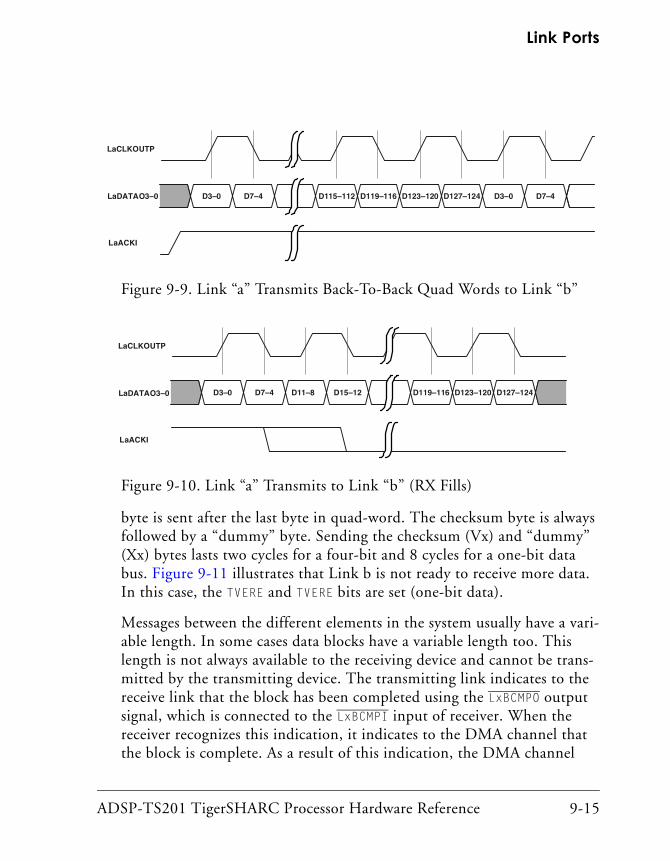
ADSP-TS201 TigerSHARC Processor Hardware Reference 9-15
Link Ports
byte is sent after the last byte in quad-word. The checksum byte is always followed by a “dummy” byte. Sending the checksum (Vx) and “dummy” (Xx) bytes lasts two cycles for a four-bit and 8 cycles for a one-bit data bus. Figure 9-11 illustrates that Link b is not ready to receive more data. In this case, the TVERE and TVERE bits are set (one-bit data).
Messages between the different elements in the system usually have a vari-able length. In some cases data blocks have a variable length too. This length is not always available to the receiving device and cannot be trans-mitted by the transmitting device. The transmitting link indicates to the receive link that the block has been completed using the LxBCMPO output signal, which is connected to the LxBCMPI input of receiver. When the receiver recognizes this indication, it indicates to the DMA channel that the block is complete. As a result of this indication, the DMA channel
Figure 9-9. Link “a” Transmits Back-To-Back Quad Words to Link “b”
Figure 9-10. Link “a” Transmits to Link “b” (RX Fills)
LaCLKOUTP
LaDATAO3–0
LaACKI
D3–0 D7–4 D115–112 D119–116 D123–120 D127–124 D3–0 D7–4
LaCLKOUTP
LaDATAO3–0
LaACKI
D3–0 D7–4 D119–116 D123–120 D127–124D15–12D11–8

Link Port Communication Protocol
9-16 ADSP-TS201 TigerSHARC Processor Hardware Reference
ignores the fact that its counter is not expired and behaves as if the block is completed. This is reflected in DMA channel status and (if programmed) interrupt and chaining operations.
The LxBCMPO signal indicates block completion by changing to low after first LxCLKOUT rising edge in the last quad-word of the block. It is set high (inactive) before the last LxCLKOUT falling edge of the same quad-word. See the ADSP-TS201 TigerSHARC Embedded Processor Data Sheet for further details. It is inactive if the TBCMPE bit is cleared in the LTCTLx register or while link transactions are executed by the processor core.
Figure 9-12 illustrates how Link “a” signals Link “b” that the current buffer has been completed.
Figure 9-11. Link “a” Transmits to Link “b” With Verification (RX Fills)
Figure 9-12. Link “a” Transmits to Link “b” With Block Completion
LaCLKOUTP
LaDATAO0
LaACKI
D0 D1 V1D127 V0 V7 X0 X7
LAST QUAD WORD IN THE CURRENT BLOCK
LaCLKOUTP
LaDATAO3–0
LaBCMPO
D3–0 D7–4 D11–8 D119–116 D123–120 D127–124

ADSP-TS201 TigerSHARC Processor Hardware Reference 9-17
Link Ports
In Figure 9-13 Link “a” signals Link “b” that the current buffer has been completed. A new quad word follows the completed block.
Link Port Transmission DelaysThe links should be able to overcome delays between the source and desti-nation. The delays of the different link signals (LxCLKOUT and LxDAT3–O) are matched to tolerances specified in the data sheet. There are two delay restrictions in the system:
• The delay of LxCLKOUT of transmitter to LxCLKIN of the receiver plus the delay of LxACKO of receiver to LxACKI of transmitter should be less than one-half quad-word transfer period.
• The difference between the trace delay of LxBCMPO and the data and clock trace delay is a maximum one-third of a quad-word transfer period.
The first restriction is that the gating factor for determining distance of operation is the round-trip propagation delay LxCLKOUT of transmitter to LxCLKIN of the receiver plus the delay of LxACKO of receiver to LxACKI of transmitter. If the transmitter sends data and the receiver signals that it is
Figure 9-13. Link “a” Transmits to Link “b” With Block Completion(A New Block From Link “a” Immediately Follows Completion of First)
LAST QUAD WORD IN THE CURRENT BLOCK
D3–0 D7–4 D11–8 D119–116 D123–120 D127–124
LaCLKOUTP
LaDATAO3–0
LaBCMPO
D3–0 D7–4 D11–8
FOLLOWING BLOCK

Link Port Transmission Delays
9-18 ADSP-TS201 TigerSHARC Processor Hardware Reference
not ready to accept more data via LxACKO, the transmitter must sample LxACKI before it sends the next transmission of data. If LxACKI is not sam-pled in time, data is lost by the receiver.
For example, while using 4-bit mode transmission, 16 link clock cycles are required to transfer one quad-word (64 cycles are required using 1-bit mode). So, 8 link clock cycles represents a one-half quad-word transfer period using 4-bit mode transmission, and 32 link clock cycles represents a one-half quad-word transfer period using 1-bit mode transmission.
Figure 9-14. Link “a” Transmits to Link “b” With Delay
LAST SAMPLEIN A QUAD WORD
LaCLKOUT
LaDATO3–0
LaACKI
LbCLKIN
LbDATI3–0
LbACKO
DELAY DELAY
SETUP

ADSP-TS201 TigerSHARC Processor Hardware Reference 9-19
Link Ports
Link Port Error Detection MechanismsThe link ports support on-the-fly error detection. When the link port detects an error condition, it operates according to the following:
1. If a time out error is detected, the TTER (Transmit Timeout Error) bit in LTSTATx or RTER (Receive Timeout Error) bit in LRSTATx is set accordingly. If the time out errors are enabled in the LRCTLx or LTCTLx registers, a hardware error interrupt is asserted. (See “Hard-ware Error Interrupt” on page 6-22.)
2. If a data overrun is detected on the receiver the ROVER bit in LRSTATx is set accordingly. If the receive overrun error is enabled in LRCTLx, a hardware error interrupt is asserted. (See “Hardware Error Interrupt” on page 6-22.)
3. If verification is enabled in LRCTLx and an incorrect checksum is detected, the RCSER bit in LRSTATx is set accordingly, and a hard-ware error interrupt is asserted. (See “Hardware Error Interrupt” on page 6-22.)
4. If an active value is written to LRCTLx or LTCTLx and the value in this control register is active, the register over write is prevented, the RWER bit is set in LRSTATx or the TWER bit is set in LTSTATx accordingly, and a hardware error interrupt is asserted. (See “Hard-ware Error Interrupt” on page 6-22.)
The error indication fields of LRSTATx and LTSTATx can be cleared by read-ing from the clear registers LRSTATCx and LTSTATCx respectively.

Link Port Error Detection Mechanisms
9-20 ADSP-TS201 TigerSHARC Processor Hardware Reference
Link Transmitter TimeoutIf the transmitter’s LxACKI is deasserted for a time period of 2048 clock cycles and the transmitter has data to transmit, a timeout error occurs, and the TTER bit is set in LTSTATx. LxACKI has a weak pull down resistor that holds it deasserted in case it is not being driven.
Unlike previous TigerSHARC processors, the ADSP-TS201 does not need or provide an optional connectivity check for error detec-tion because the transmit timeout and pull-down on LxACKI are sufficient for detecting that a receiver is not connected.
Link Receiver TimeoutIf the receiver has its receive buffer full but there is not any read access to it for 2048 clock cycles, a time-out error occurs, and the RTER bit is set in LRSTATx.
Link Verification ErrorThe transmitter creates and sends a special verification byte on every transmitted quad word (if it is enabled). This byte is a checksum calcu-lated from all data bytes that have been transmitted. It is sent at the end of every 16-byte (quad word) transmission. The receiver compares the trans-mitted verification byte to the local verification byte created during data reception. If the two bytes differ, the RCSER bit is set in the LSTATx register and a hardware interrupt is issued.
The checksum algorithm is:
Checksum = Least-Significant-Byte of (B0 + B1 + … + B15)
where B0, B1, and so on are byte1, byte2 …

ADSP-TS201 TigerSHARC Processor Hardware Reference 9-21
Link Ports
Link Transmit/Receive Write ErrorWriting an active value into transmit or receive control register is legal only when the corresponding register is inactive. Writing an active value to an active control register does not succeed and causes a write error.
Link Port Control RegistersThe ADSP-TS201 processor’s link control register is split into two control registers—receive link control register (LRCTLx) and transmit control regis-ter (LTCTLx). These registers define the flavor of the link protocol that is used in a specific application. These registers are not to be changed during link operation.
Writing to a control register an active value is allowed only when the reg-ister has an inactive value (LREN in LRCTL or LTEN in LTCTL are cleared). In order to change the setup while link is running, an inactive value has to be

Link Port Control Registers
9-22 ADSP-TS201 TigerSHARC Processor Hardware Reference
written to stop operation of the link, and then the new active value should be written. Ignoring this rule shall cause a hardware error interrupt, and the new value will not be written.
15 14 13 12 11 10 9 8 7 6 5 4 3 2 1 0
0 0 0 0 0 0 0 0 0 0 0 0 0 0 0 1
REN Receive Enable1=enable, 0=disable
RVERE Verification Enable1=enable, 0=disable
RTOE Receive Time Out Check IRQ Enable1=enable, 0=disable
RBCMPE Receive Block Completion1=enable LxBCMPI input detection,0=disable LxBCMPI input detection
RDSIZE Data Size1 1=4 bit data, 0=1 bit data
1 The reset value of the RDSIZE bit depends on the value of the LINK_DWIDTH strap pin at reset. If LINK_DWIDTH=0 at reset, RDSIZE=0 (1 bit data).
ROVRE Receive Overrun Error IRQ Enable1=enable, 0=disable
RINIF Receive Initialization Forced1=force RINIV value, 0=not forced
RINIV Receive Initialization Value1=use 1 for data, 0=use 0 for data
Reserved
Figure 9-15. LRCTLx Low (Lower) Register Bit Descriptions2
2 The upper 16 bits (31–16) of LRCTLx are reserved (=0)

ADSP-TS201 TigerSHARC Processor Hardware Reference 9-23
Link Ports
Table 9-4. LRCTLx Register
Reset Value = 0x0000 0001 (if LINK_DWIDTH, Reset Value = 0x0000 0011)
Bit Field Definition Default
0 REN Link Receive Enable. When cleared, the receive channel goes to idle state. LxACKO is driven low. On reset, the REN set.
1
1 RVERE Verification Enable. Enables checksum verification for received data. On reset, this bit is cleared.
0
2 RTOE Time-Out Enable. Enables interrupt on timeout check for received data. On reset, this bit is cleared.
0
3 RBCMPE Block Completion Enable. Enables the receiver to signal the DMA that the whole block has been received. On reset, this bit is cleared.
0
4 RDSIZE
Data Size1. 0: 1 bit1: 4 bitsFor LRCTLx, on reset this bit gets its value of the strap “LINK_DWIDTH”.
0,1
5 ROVRE Over-Run Enable 0
6 RINIF Rx initialized state forced by software enable 0
7 RINIV Rx initialized state forced value enable 0
31–8 Reserved N/A 0
1 The reset value of the RDSIZE bit in LRCTLx depends on the setting for the LINK_DWIDTH strap pin.
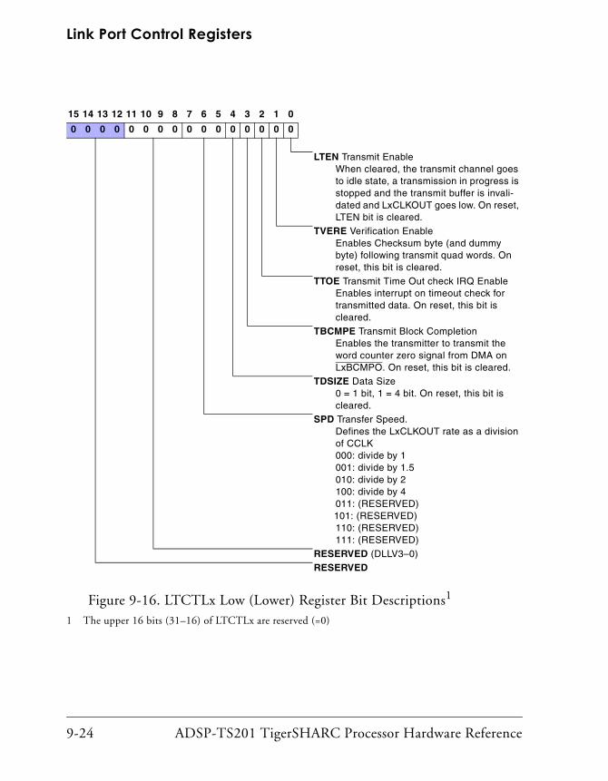
Link Port Control Registers
9-24 ADSP-TS201 TigerSHARC Processor Hardware Reference
15 14 13 12 11 10 9 8 7 6 5 4 3 2 1 0
0 0 0 0 0 0 0 0 0 0 0 0 0 0 0 0
LTEN Transmit EnableWhen cleared, the transmit channel goes to idle state, a transmission in progress is stopped and the transmit buffer is invali-dated and LxCLKOUT goes low. On reset, LTEN bit is cleared.
TVERE Verification EnableEnables Checksum byte (and dummy byte) following transmit quad words. On reset, this bit is cleared.
TTOE Transmit Time Out check IRQ EnableEnables interrupt on timeout check for transmitted data. On reset, this bit is cleared.
TBCMPE Transmit Block CompletionEnables the transmitter to transmit the word counter zero signal from DMA on LxBCMPO. On reset, this bit is cleared.
TDSIZE Data Size 0 = 1 bit, 1 = 4 bit. On reset, this bit is cleared.
SPD Transfer Speed.Defines the LxCLKOUT rate as a division of CCLK000: divide by 1001: divide by 1.5010: divide by 2100: divide by 4011: (RESERVED)
101: (RESERVED)110: (RESERVED)111: (RESERVED)
RESERVED (DLLV3–0)RESERVED
Figure 9-16. LTCTLx Low (Lower) Register Bit Descriptions1
1 The upper 16 bits (31–16) of LTCTLx are reserved (=0)

ADSP-TS201 TigerSHARC Processor Hardware Reference 9-25
Link Ports
Table 9-5. LTCTLx Register1
Reset Value = 0x0000 0000
Bit Field Definition Default
0 LTEN Link Transmit Enable. When cleared, the transmit channel goes to idle state, a transmission in progress is stopped and the trans-mit buffer is invalidated and LxCLKOUT goes low. On reset, LTEN bit is cleared.
0
1 TVERE Verification Enable. Enables Checksum byte (and dummy byte) following transmit quad words. On reset, this bit is cleared.
0
2 TTOE Time-Out Enable.Enables interrupt on timeout check for trans-mitted data. On reset, this bit is cleared.
0
3 TBCMPE Block Comp. Enable. be Enables the transmitter to transmit the word counter zero signal from DMA on LxBCMPO. On reset, this bit is cleared.
0
4 TDSIZE Data Size. 0 = 1 bit data, 1 = 4 bit data. On reset, this bit is cleared.
0
7–5 SPD2–0 Transfer Speed 0
11–8 Reserved DLLV3–0 0
31–12 Reserved N/A 0
1 See “Link Port Control Registers” on page 9-21.

Link Port Status Registers
9-26 ADSP-TS201 TigerSHARC Processor Hardware Reference
Link Port Status RegistersThe link status register is split into two status registers – receive link status register (LRSTATx) and transmit status register (LTSTATx). These registers show the link runtime status. These registers are read-only registers.
15 14 13 12 11 10 9 8 7 6 5 4 3 2 1 0
0 0 0 0 0 0 0 0 0 0 0 0 0 0 0 0
RSTAT Receive buffers status00: buffer empty01: buffer valid (can still receive)11: buffer full10: buffer not ready (data transient)
RTER Receive timeout error indication1=error, 0=no error
RWER Receive write error1=error, 0=no error
RCSER Receiver checksum error1=error, 0=no error
ROVER Receive overrun error1=error, 0=no error
RINIT Receiver initialization status1=initialized, 0=not initialized
Reserved
Figure 9-17. LRSTATx Low (Lower) Register Bit Descriptions1
1 The upper 16 bits (31–16) of LRSTATx are reserved (=0)

ADSP-TS201 TigerSHARC Processor Hardware Reference 9-27
Link Ports
Table 9-6. LRSTATx Register1
Reset Value = 0x0000 0000
Bit Field Definition Default
1–0 RSTAT1–0 Receive Status. 00: buffer empty01: buffer valid (can still receive)11: buffer full and data valid10: buffer not available because of synchronization problem — data not ready (in transient temporary state)
0
2 RTER Time-Out Error 0
3 RWER Write Error. an active value was written to control register when previous value of control register was active.
0
4 RCSER Check Sum Error 0
5 ROVER Over-Run Error 0
6 RINIT Receiver initialization status 0
31–7 Reserved N/A 0
1 See “Link Port Status Registers” on page 9-26.

Link Port Status Registers
9-28 ADSP-TS201 TigerSHARC Processor Hardware Reference
15 14 13 12 11 10 9 8 7 6 5 4 3 2 1 0
0 0 0 0 0 0 0 0 0 0 0 0 0 0 0 0
TVACANT Transmitter VacantWhen set, the transmitter is vacant—data for transmit can be written to transmit buffer.Note: After enabling the transmitter (LTEN bit set in LTCTLx) it takes up to 800 SOC-CLK cycles for this bit to assert.
TEMPTY Transmit is empty.When set, transmit is empty and all data that has been written to the transmit buffer has been transmitted.Note: This should be tested before dis-abling the channel.
TTER Transmit timeout errorindication.
TWER Transmit write error – an active value was written to control register when previ-ous value of control register was active
RESERVED
Figure 9-18. LTSTATx Low (Lower) Register Bit Descriptions1
1 The upper 16 bits (31–16) of LTSTATx are reserved (=0)

ADSP-TS201 TigerSHARC Processor Hardware Reference 9-29
Link Ports
Table 9-7. LTSTATx Register1
Reset Value = 0x0000 0002
Bit Field Definition Default
0 TVACANT Transmit Vacant. When set, the transmitter is vacant—data for transmit can be written to transmit buffer.Note: After enabling the transmitter (LTEN bit set in LTCTLx) it takes up to 800 SOCCLK cycles for this bit to assert.
0
1 TEMPTY Transmit Empty. When set, transmit is empty and all data that has been written to the transmit buffer has been transmit-ted.Note: This should be tested before disabling the channel.
1
2 TTER Time-Out Error 0
3 TWER Write Error. – an active value was written to control register when previ-ous value of control register was active
0
31–4 Reserved N/A 0
1 See “Link Port Status Registers” on page 9-26.

Link Port Status Registers
9-30 ADSP-TS201 TigerSHARC Processor Hardware Reference

ADSP-TS201 TigerSHARC Processor Hardware Reference 10-1
10 JTAG PORT ANDTEST/DEBUG INTERFACE
The functionality described in this chapter is useful for both software debugging and services usually found in operating system (OS) kernels. These features are implemented in the TigerSHARC processor hardware to allow debuggers and operating systems to build the more complex aspects of their features. The functionality is grouped into levels. These levels build upon each other to allow greater control and visibility of the TigerSHARC processor for the debugger or kernel.
The debugging approach is based on the idea of protected execution (user mode) and unprotected execution (supervisor mode). In user mode, some of the system resources can be made accessible. However, when those resources must be managed by an OS kernel, they are restricted. When user code tries to access a protected resource, an exception occurs and the access is aborted.
The debugger can control the TigerSHARC processor in one of two ways:
• Using a debug monitor (running in supervisor mode)
• Using an In-circuit emulator (ICE)
In supervisor mode, some system resources are allocated to the monitor. (For example, memory, communication channel-to-host, interrupt, flag bits, and so on.)
The ICE, by comparison, uses a reserved communication channel (the JTAG test access port) to control the TigerSHARC processor. This way the ICE can be non-intrusive to the system, as well as control systems that cannot communicate with a host system.

10-2 ADSP-TS201 TigerSHARC Processor Hardware Reference
As shown in Figure 10-1, the JTAG port is a bus slave on the SOC bus. It is important to note that debug register accesses must cross a number of clock domains when reading or writing register data. Corresponding response for emulator software exceptions may vary with SOC bus load-ing. Because the emulator interrupt (an interrupt input to the interrupt unit) has a direct connection to the program sequencer, response to latched emulator interrupts is not affected by SOC bus loading. For more information on clock domains, see “SOC Interface” on page 3-1.
Since many of the functions needed by the debug monitor and the ICE overlap, most of the debug functions in the TigerSHARC processor are shared between the two methods. There are some features that need to be optionally restricted by the ICE so that the debugger can be used in super-visor mode.
Debug capabilities are available either through the ICE or through the supervisor mode. As already mentioned, the ICE mode is accessed through the JTAG port. The supervisor mode is entered via an interrupt, an excep-tion, or a specific software watchpoint. When the TigerSHARC processor is in supervisor or emulation mode, it has complete access to all of the TigerSHARC processor’s resources.

ADSP-TS201 TigerSHARC Processor Hardware Reference 10-3
JTAG Port and Test/Debug Interface
Figure 10-1. JTAG Port and SOC Bus Connections
S-Bus
Memory
I-Bus
K-Bus
J-Bus
Processor CoreCompute Blocks
Integer ALUsSequencer
Non-Ureg Registers
SOCInterface
LinkPorts
ExternalPort (EBIU)
JTAGPort DMA
Timer
Interrupts
SOCBus
Flags
ClusterBus
128 Bits WideOperates at SOCCLK rate
Each128 Bits
WideOperateat CCLK
rate
64 Bits WideOperates atSCLK rate
Operate atLxCLKIN/OUT
rate
Extended CoreOperates atCCLK rate
Operate atSCLK rateOperates at
TCK rate
Interrupt Vector
FLAGx TMR0E DMARxIRQx

Operating Modes
10-4 ADSP-TS201 TigerSHARC Processor Hardware Reference
Table 10-1 details debug concepts and capabilities.
Operating ModesThe TigerSHARC processor operates in one of three modes—emulator, supervisor, and user. In user and supervisor modes, all instructions are executed normally. In user mode, however, the register access is limited. In emulation mode, none of the control flow instructions (excluding If
Table 10-1. Debug Concepts
Debug Tools Debug Feature
Watchpoints Allows a user to specify particular watchpoint address ranges and conditions that halt the processor when those conditions are met. The user can then examine the state of the processor, restore that state, and continue instruction execution. Software breakpoints and single step are implemented using watchpoint as well.
Multiprocessing Capability
Allows a user to single step and set breakpoints in a multiproces-sor system.
Trace History Allows a trace of the program counter to be recreated. An on-chip trace buffer (FIFO) stores the last eight branches (all discontinu-ous values of the program counter) taken by the program sequencer, allowing the recent program path to be recreated.
Cycle Count Provides the basic functionality for all code profiling functions.
Performance Monitoring
Allows internal resources to be monitored unobtrusively. The debugger can specify which internal resource(s) should be monitored.
Access to Protected Registers Provides access to protected registers. Protected registers are only accessible in supervisor mode or ICE. They cannot be accessed by user mode and are protected from accidental modifications that could cause system damage.
Watchpoint Counters Allows the user to search for the nth occurrence of an event before halting.
Exception Aborts execution of the next and the following piped instructions. For more information, see “Handling Exceptions” on page 6-15.

ADSP-TS201 TigerSHARC Processor Hardware Reference 10-5
JTAG Port and Test/Debug Interface
True, RTI (np);) may be used—control flow instructions may cause problems and it is illegal to use them in emulation. Operating modes are discussed in “Operation Modes” on page 1-18.
Debug ResourcesThe processor provides a number of debug resources, including:
• “Special Instructions” on page 10-5
• “Watchpoints” on page 10-5
• “Instruction Address Trace Buffer (TBUF)” on page 10-8
Special InstructionsThe TigerSHARC processor supports special instructions (traps) which are used to aid system debugging. These instructions are required to implement both software breakpoints (in debuggers) and operating system calls (for OS kernels).
WatchpointsAddress watchpoints allow the user to examine the state of the processor whenever a set of user-defined memory access conditions occurs.
There are three watchpoint sets that can operate in parallel. At each watchpoint, the user can define conditions for bus access cycles and the operation the TigerSHARC processor should execute when these occur.
Programming – Control and Address Pointer Registers
Each watchpoint has two address registers—WPiL and WPiH. See “Watch-point Address Pointer (WPxL/WPxH) Registers” on page 2-89 for more information. When the watchpoint is programmed for a single address,

Debug Resources
10-6 ADSP-TS201 TigerSHARC Processor Hardware Reference
only the low address register (WPiL) is used. If the watchpoint is searching for an address range, the WPiL holds the low address, and the WPiH holds the high address.
It is important to set the Address Pointer registers first (before the WPiCTL register) which define the actual watchpoint operation. The address regis-ters of a watchpoint cannot be changed when the watchpoint is active.
A watchpoint operation is defined by its Control register—WPiCTL (where i is 0, 1, or 2 for different watchpoints). Figure 2-46 on page 2-86, Figure 2-47 on page 2-87, and Figure 2-48 on page 2-88 show the config-uration of the WPiCTL registers.
Watchpoint Operation
The following information must be programmed into the Watchpoint registers before a search can begin:
• Address or address range
• Count
When the control register is set to a non-idle operation, the count field is set to the initial count. After the count field is reset, the watchpoint hard-ware monitors the internal buses for a transaction address matching what is specified in the watchpoint address registers.
Whenever there is a match, the counter is decremented.
After the counter reaches zero, an exception is initiated—either a software exception or an emulator trap according to Bits3–2 in the EXtype field in WPiCTL. At this point, the Status register indicates ‘watchpoint count expired’. To begin another search, the user must rewrite the control register.

ADSP-TS201 TigerSHARC Processor Hardware Reference 10-7
JTAG Port and Test/Debug Interface
The three watchpoints are associated with different buses. Watchpoint 0 is used to monitor instruction fetches on the I-bus. Watchpoint 0 supports a single step option (SSTP) which is used by emulation to perform single step operations. Watchpoint 1 is used to monitor data accesses over the J- and K-buses. Watchpoint 1 supports detection of accesses by either J, K, or both. Watchpoint 1 also supports detection of read accesses only, write accesses only, or both. Watchpoint 2 is used to monitor data accesses over the S-bus. Watchpoint 2 supports detection of read accesses only, write accesses only, or both.
Watchpoint Status (WPiSTAT)
The WPiSTAT register indicates the current status of the search. It holds the current count of the search and the mode the watchpoint is executing. When the counter expires, the watchpoint status Bits17–16 change to 11.
31 30 29 28 27 26 25 24 23 22 21 20 19 18 17 16
0 0 0 0 0 0 0 0 0 0 0 0 0 0 0 0
ReservedEX Execution
Figure 10-2. WPxSTAT (Upper) Register Bit Descriptions1
1 The lower 16 bits of WPxSTAT (not shown) are the watch point current count.
Table 10-2. WPiSTAT Register Bit Descriptions
Bits Name Description
15–0 VALUE Watchpoint ValueDetermines the current value of the watchpoint counter.
17–16 EX Execution BitWatchpoint is executing00 – Watchpoint disabled01 – Searching for match11 – Watchpoint count expired
31–18 Reserved Reserved

Performance Monitors
10-8 ADSP-TS201 TigerSHARC Processor Hardware Reference
Instruction Address Trace Buffer (TBUF)Since the program counter is not accessible in real time off chip when exe-cuting instructions from internal memory, a trace buffer has been provided to assist code debugging.
The trace buffer is an eight register list that stores a history of the last four to eight branches taken by the program sequencer, allowing the user to fully recreate the path the program took for the last eight branches.
The branches are written into the eight Trace Buffer registers in a circular manner. The first is written into TRCB0, the next into TRCB1, and so on until TRCB7. The ninth branch is written back into TRCB0, and so on. In order to ascertain the last register, the user must refer to the Trace Buffer pointer register, which points to the last written entry.
The trace buffer always holds the PC of the branch instruction line. In case of a computed branch, it also stores the target PC of the branch on the next entry. To distinguish between the jump PC and the target PC, the TRCBMASK should be used. Every bit in the TRCBMASK is associated with the corresponding TRCBi register. If it is cleared, the TRCBi holds the PC of the jump instruction line. If set, the TRCBi holds the target PC of the jump.
Performance MonitorsThe performance monitors are targeted to optimize the functioning of a working application. The monitors provide indications of how many times an event occurs during a specific run. These monitors are con-structed of three registers—cycle counter, performance monitor mask, and performance monitor counter. The cycle counter and performance moni-tor should be initialized to zero by the user before a specific run. The ratio between the total count and the performance monitor counter gives the required indication.

ADSP-TS201 TigerSHARC Processor Hardware Reference 10-9
JTAG Port and Test/Debug Interface
When the performance monitor counter expires, it issues an exception.
Cycle Counter (CCNT1–0)CCNT1–0 counts cycles while the program is executing. All cycles are counted. The cycle counter is a 64-bit counter that increments with every cycle, including executions in both user and supervisor modes. All hold, wait state, aborted instructions, and other delay cycles are also counted.
When the TigerSHARC processor enters emulator mode, the cycle counter halts, since it is irrelevant.
Performance Monitor Mask – PRFMThe Performance Monitor Mask is a 32-bit register that defines the events that are monitored by the performance counters. Every bit in the Perfor-mance Monitor refers to an event that reflects the application performance (for example, the number of stall cycles in the system). See “Performance Monitor Mask (PRFM) Register” on page 2-89.
When only one bit in the PRFM register is set, the feature indicated by this bit is counted while the TigerSHARC processor is running in user and supervisor mode. The count is halted when the TigerSHARC processor is in emulation mode. For certain events (for example, compute block instructions or bus transactions), the counter may compute more than one transaction/instruction every cycle, according to the event occurrence.
When more than one bit is set in the mask, the count is according to the SUM bit (Bit 31). If the SUM bit is clear, and more than one bit in the Per-formance Mask is set, PRFCNT counts every cycle where one of the events occurs. The counter, however, does not sum the events but ORs them. If the SUM bit is set, the events are summed. In this case, on a cycle where the compute block (X or Y) executes two instructions, the counter is incre-mented by two, and on bus transactions (Bits14–12) the counter could be incremented by three.

Performance Monitors
10-10 ADSP-TS201 TigerSHARC Processor Hardware Reference
Where the SUM bit is set, there are restrictions on the different events that can be combined. The set bits must be a subset of one of the following groups.
• Bits11–0 – granted or non granted bus requests
• Bits20–12 – transactions per bus
• Bits29–21 – instructions
The Performance Monitor Mask is disabled by clearing all bits in the mask.
Performance Monitor CounterThe Performance Monitor counts the events according to the pro-grammed mask. It counts the events while the TigerSHARC processor is in user or supervisor mode.

ADSP-TS201 TigerSHARC Processor Hardware Reference 10-11
JTAG Port and Test/Debug Interface
JTAG FunctionalityThe TigerSHARC processor supports the IEEE Standard 1149.1 Test Access Port.
JTAG Port I/O PinsTable 10-3 describes those TigerSHARC processor pins used by JTAG emulation hardware. Underlined or overbarred pin names indicate nega-tive true signals.
Table 10-3. JTAG and Emulation I/O Pins
Signal Type Description
TRST InputAsynchronous
Test Reset (JTAG)Resets the test state machine. The TRST signal must be asserted after power up to ensure proper JTAG operation. The TRST signal has a 40 kΩ internal pull-up resistor.
TCK Input Test Clock (JTAG)Provides an asynchronous clock for JTAG boundary scan.
TDI Input Test Data Input (JTAG)A serial data input of the boundary scan path. This signal has a 40 kΩ internal pull-up resistor.
TDO Output Test Data Output (JTAG)A serial data output of the boundary scan path.
TMS Input Test Mode Select (JTAG)Controls the test state machine. This signal has a 40 kΩ internal pull-up resistor.
EMU Output EmulationConnected to the ADSP-TS201 DSP EZ-ICE target board connector only.

JTAG Functionality
10-12 ADSP-TS201 TigerSHARC Processor Hardware Reference
As an extension to the JTAG standard, the TMS and EMU pins have these additional debugging functions:
• The TMS pin (when TEME bit in the EMUCTL register is set) functions as an emulation exception pin. An emulation exception is issued on every rising edge of the TMS signal. This function is in addition to TMS functionality in JTAG.
• The EMU output is an open drain signal (for wired OR) driven only if the EMUOE bit in the EMUCTL register is set. The EMU pin gives the following indications:
• On watchpoint event no exception (EXtype field in WPiCTL) is 00, the EMU is pulled down for 20 CCLK cycles.
• Whenever the TigerSHARC processor is in emulation mode and ready for a new instruction line driven into the EMUIR register, the EMU pin is driven low until such an instruction is inserted. For more information, see “Emulator Mode” on page 1-20.

ADSP-TS201 TigerSHARC Processor Hardware Reference 10-13
JTAG Port and Test/Debug Interface
JTAG Instruction RegisterThe JTAG Instruction register is five bits long and allows the Test Access Port (TAP) controller to select any of the scannable data registers. The LSB is the first to be shifted out through the TDO. The encoding of this Instruction register follows the TigerSHARC processor implementation.
Data RegistersThe Data registers are selected via the Instruction register. Once a particu-lar Data register’s value is written into the Instruction register, and the TAP state is changed to SHIFT-DR, the particular data going in and out of the TigerSHARC processor depends on the definition of the Data register selected. See the IEEE 1149.1 specification for more details.
Table 10-4. JTAG Port Access Instruction Decode
If IR4–0 Value is... Corresponding Instruction is... To...
00000 EXTEST Execute EXTEST
10000 Sample/Preload Execute sample and preload
01000 EMUIR Scan in EMUIR register
10100 EMUDAT Scan EMUDAT register
01110 IDCODE Scan ID code register
11110 SAMPLEPC Sample PC from which the TigerSHARC processor is running
10001 EMUTRAP Execute an emulation trap
10011 OSPID Scan OSPID register
00100 EMUCTL Scan EMUCTL register
01100 EMUSTAT Scan EMUSTAT register
11111 BYPASS Bypass

JTAG Functionality
10-14 ADSP-TS201 TigerSHARC Processor Hardware Reference
When registers are scanned out of the device, the LSB is the first bit to go out of the TigerSHARC processor.
The data registers are:
• Bypass
A IEEE 1149.1 required register, this is a one (1) bit register.
• Boundary
Registers used by multiple JTAG instructions. All three of the JTAG instructions that use the boundary are required by the IEEE 1149.1 specification.
• EMUIR
The JTAG instruction loads 48 bits, of which the 32 LSBs are loaded into the EMUIR register. The EMUIR is a 128-bit register. In emulation mode the register is loaded four times in a sequence (with the same JTAG instruction) or is loaded until one word has the EX bit set (then the rest of the EMUIR slots are considered NOPs); and each time the data is loaded into the next word in EMUIR—Bits31–0 are loaded first, next Bits63–32 are loaded, and so on.
When the four EMUIR loads have completed (or the instruction line was completed with the EX bit set), the instructions that were loaded to the JTAG are fed into the sequencer and executed.
When a quad-word is loaded into EMUIR, it should include one full instruction line. The instruction line must not continue to the next quad-word. In this case the last slots have to be filled with “no operation” (NOP) instructions. Except for the restriction of not

ADSP-TS201 TigerSHARC Processor Hardware Reference 10-15
JTAG Port and Test/Debug Interface
crossing the quad-word boundary, this is similar to the assembler coding described in “Instruction Set” in the ADSP-TS201 TigerSHARC Processor Programming Reference.
Writing to EMUIR when the TigerSHARC processor is not in emu-lator mode is an illegal operation.
• EMUDAT
This is a 48-bit register whose 32 MSBs are used to scan the Ureg of the same name. The emulator uses this register to read and set all other registers in the TigerSHARC processor.
The emulator also uses this register to access memory. There must be an instruction that uses the IALUs to generate the address for the memory access whose target or source is EMUDAT. When the emulator executes a series of memory accesses, the TigerSHARC processor should insert hold cycles to allow all of the accesses to complete (just as it does normally).

JTAG Functionality
10-16 ADSP-TS201 TigerSHARC Processor Hardware Reference

ADSP-TS201 TigerSHARC Processor Hardware Reference 11-1
11 SYSTEM DESIGN
This chapter provides information that is useful for developing ADSP-TS201 TigerSHARC processor based systems and applications. There are descriptions of how to use the TigerSHARC processor in single processor implementations, in multiple TigerSHARC processor designs, and in testing scenarios. Hardware, software, and system design informa-tion are included.
When engineers are designing a system that includes the ADSP-TS201 TigerSHARC processor, they need a number of documentation resources including manuals, data sheets, and engineer-to-engineer notes. Many of these documents are identified in the reference sections:
• “Booting References” on page 11-8
• “Hardware Design References” on page 11-17
• “Thermal Design References” on page 11-27
• “Other Design and Test References” on page 11-28
• “Recommended Reading References” on page 11-31
Included in both Analog Devices manuals and data sheet are references of source materials, such as Engineer-to-Engineer Notes or Application Notes, available on the Internet. The documents listed here are considered to be essential to any design involving the ADSP-TS201 TigerSHARC processor and are maintained in the form of Engineer-to-Engineer notes due to the dynamic nature of this information and the capability to update these documents more easily whenever it may become necessary.

Processor Booting Methods
11-2 ADSP-TS201 TigerSHARC Processor Hardware Reference
The application and engineer-to-engineer notes from Analog Devices that are mentioned in this chapter are available at:
http://www.analog.com/dsp/appnotes
Processor Booting MethodsThis section explains the functional operation booting methods and pro-vides a high-level overview of available boot loader kernels (booting software) for the ADSP-TS20x TigerSHARC processors.
This section includes information on boot kernels for ADSP-TS201S and ADSP-TS202S processors. Boot kernels for ADSP-TS203S processors form a subset of the discussed functionality because this processor has only two link ports and a 32-bit external bus. Except for these restrictions, the information in this section applies to all ADSP-TS20x processors.
It is important to note that the information in this section, while considered complete and accurate when printed, may be updated as new information becomes available. Please use the information in any versions of ADSP-TS20x TigerSHARC Processor Boot Loader Kernels Operation (EE-200) engineer-to-engineer note that are published after the publication date of this book.
After reset, the ADSP-TS20xS has four boot options for beginning opera-tion: EPROM boot, host boot, link port boot, and no boot. Systems select among these options using strap mode pins. After the boot mode is selected, the processor boot loads (if in a master mode) or is boot loaded (if in a slave mode) with 256 words of boot data. Typically, this boot data contains the boot kernel for the selected mode. After this initial load is complete, the boot kernel executes, loading the developer’s program into the processor and starting execution of that program.

ADSP-TS201 TigerSHARC Processor Hardware Reference 11-3
System Design
Using Boot Modes and Boot Loader KernelsA loader kernel is a program executed by the processor that is appended to user application code by the elfloader utility (elfloader.exe) of the VisualDSP++® development tools. The processor executes the loader ker-nel at boot time, allowing the processor to initialize its internal and external memory sections defined in the application code.
The loader kernel is a self-modifying program that is transferred into the processor’s internal memory. The ADSP-TS20x family of processors sup-ports three booting methods: EPROM booting (via the external port), host booting (via an external host processor or another ADSP-TS20x pro-cessor), and link booting (via the processor’s link ports). VisualDSP++ includes three distinct loader kernels that support each of the processor’s booting modes. Additionally, there are several no-boot modes, which do not require kernels.
To understand the booting process for each of the boot modes in further detail, please refer to the ADSP-TS20x TigerSHARC Proces-sor Boot Loader Kernels Operation (EE-200) engineer-to-engineer note.
Executing a Processor Boot OperationThe booting mode is selected by the processor’s BMS pin. While the proces-sor is held in reset, the BMS pin is an active input. If BMS is sampled low a certain number of SCLK cycles after reset, EPROM boot mode is selected; a number of SCLK cycles after this, the BMS pin becomes an output and serves as the EPROM chip select. If BMS is sampled high instead, the ADSP-TS20x processor is in an idle state, waiting for a host boot or a link port boot to occur. The exact timing for sampling BMS boot strap and fol-lowing driving of BMS is provided in the processor’s data sheet.

Processor Booting Methods
11-4 ADSP-TS201 TigerSHARC Processor Hardware Reference
At reset, a weak internal pull-down resistor is on the BMS pin. Depending upon the external line loading on this pin, this pull-down resistor may not be sufficient. You may need to add an external pull-down resistor to select EPROM booting mode. If host or link boot is desired, BMS must be held high during and after reset and may be tied directly to VDD_IO, provided it is never used as a chip select.
Each booting method is described in detail in the following sections.
EPROM Boot
Booting the processor from an EPROM is a master boot mode—a boot mode in which the TigerSHARC processor starts and controls the external data fetch process.
The ADSP-TS20xS processor defaults to EPROM booting depending on the value of the BMS strap pin. When the processor is configured to boot from EPROM, BMS is active during the boot sequence and should be con-nected to the chip select signal of the EPROM. For additional information refer to the BMS strap pin section.
When EPROM boot mode is selected, the ADSP-TS20x processor initial-izes its external port DMA channel 0 to transfer 256 32-bit words of code from the boot EPROM into memory block 0 locations 0x00-0xFF of the ADSP-TS20x processor. The corresponding interrupt vector (for DMA channel 0) is initialized to internal memory address 0x00. Upon comple-tion of the DMA, the ADSP-TS20x processor continues program execution from address location 0x00. These 256 words of code act as a boot loader to initialize the rest of the ADSP-TS20x processor’s memory. The VisualDSP++ development tools provide a default boot loader kernel source file (TS201_prom.asm). For more information on this boot kernel, see the ADSP-TS20x TigerSHARC Processor Boot Loader Kernels Operation (EE-200) engineer-to-engineer note.
ADSP-TS201 TigerSHARC Processor Hardware Reference 11-5
System Design
Host Boot
Booting the processor from a host is a slave boot mode—a boot mode in which the TigerSHARC processor expects an external device to start and control the placement of code in the processor’s memory.
The ADSP-TS20xS processor supports booting from an external master (host or another ADSP-TS20xS). Any master on the cluster bus can boot the ADSP-TS20xS through writes to its internal memory or through autoDMA.
To configure the processor for host boot, place a pullup resistor between BMS and VDD_IO. For resistor value information, see the ADSP-TS201S TigerSHARC Embedded Processor Data Sheet.
When a host or link boot mode is selected, the ADSP-TS20x processor enters an idle state after reset, waiting for the external host processor or link port to boot it. Host booting uses the ADSP-TS20x processor’s AUTODMA registers (either channel), both of which are initialized to transfer 256 words of code to block 0, locations 0x00-0xFF of the ADSP-TS20x processor’s internal memory. The corresponding interrupt vector is initialized to point to address 0x00. Thus, upon completion of the DMA, the ADSP-TS20x processor continues execution at memory location 0x00. These 256 words of code act as a boot loader to initialize the rest of the ADSP-TS20x processor’s memory. The VisualDSP++ development tools supplies a default boot loader, named TS201_host.asm. For more information on this boot kernel, see the ADSP-TS20x TigerSHARC Processor Boot Loader Kernels Operation (EE-200) engineer-to-engineer note.
An example code of a ADSP-TS20x processor acting as a master, host booting another ADSP-TS20x processor is provided with the examples for the ADSP-TS201S EZ-KIT Lite™ development system.

11-6 ADSP-TS201 TigerSHARC Processor Hardware Reference
Link Port Boot
Booting the processor from a link port is a slave boot mode—a boot mode in which the TigerSHARC processor expects an external device to start and control the placement of code in the processor’s memory.
All four receive link port DMA channels are initialized after reset to trans-fer a 256-word block to internal memory addresses 0 through 255, and to issue an interrupt at the end of the block (similar to an external port DMA). The corresponding DMA interrupts are set to address zero. For additional information refer to the BMS and TMR0E strap pin sections.
To configure the processor for Link Port boot place a pullup resistor between BMS and VDD_IO. For resistor value information, see the ADSP-TS201S TigerSHARC Embedded Processor Data Sheet.
When a host or link boot mode is selected, the ADSP-TS20x processor enters an idle state after reset, waiting for the host or link port to boot it. A link boot can use any of the ADSP-TS20x processor’s link ports, all of whose DMAs are initialized to transfer 256 words of code to ADSP-TS20x processor’s memory block 0, locations 0x00-0xFF. The corresponding DMA interrupt vectors are initialized to 0. Thus, upon completion of the link DMA, the ADSP-TS20x processor continues execution at location 0x00. These 256 words of code act as a boot loader to initialize the rest of ADSP-TS20x processor’s memory. Analog Devices supplies a default boot loader, TS201_link.asm, with the VisualDSP++ tools set. For more infor-mation on this boot kernel, see the ADSP-TS20x TigerSHARC Processor Boot Loader Kernels Operation (EE-200) engineer-to-engineer note.
No Boot
Starting the processor in no boot is a master boot mode—a boot mode in which the TigerSHARC processor starts and controls the external data fetch process. In no boot mode, the TigerSHARC processor starts from an IRQ vector (externally or internally) fetching data.

ADSP-TS201 TigerSHARC Processor Hardware Reference 11-7
System Design
The ADSP-TS20xS processor begins execution from the memory address selected with one of the IRQ3-0 interrupt signals. Using the ‘no boot’ option, the ADSP-TS20xS starts running from memory when one of the interrupts is asserted. For additional information refer to the BMS and BM strap pin sections.
To configure the processor for No boot (boot from memory address) place a pullup resistor from BM to VDD_IO and place a pullup resistor from BMS to VDD_IO. For resistor value information, see the ADSP-TS201S TigerSHARC Embedded Processor Data Sheet.
When a host or link boot mode is selected, the ADSP-TS20x processor enters an idle state after reset, waiting for the host or link port to boot it. It does not have to be booted by the host or a link port. If external inter-rupts IRQ3–0 are enabled (selected at reset by the IRQEN strap pin), they can be used to force code execution according to the default interrupt vec-tors, as shown in Table 11-1.
In this scenario, another device, such as a host processor, initializes the appropriate memory with the appropriate code and then forces the corre-sponding interrupt.
Another no-boot method of starting up the ADSP-TS20x processor is for a host to initialize a memory buffer with code and then force that code execution via a vector interrupt.
Table 11-1. IRQ3–0 Default Interrupt Vectors
Interrupt Address
IRQ0 0x30000000 (MS0)
IRQ1 0x38000000 (MS1)
IRQ2 0x80000000 (MSH)
IRQ3 0x00000000 (Internal Memory)

Hardware System Design Guidelines
11-8 ADSP-TS201 TigerSHARC Processor Hardware Reference
Many intricate details must be addressed when the chip is started up. The standard supplied boot loader kernels take care of those details, so system start up based on those loaders is highly recommended.
Booting ReferencesThe following documents from Analog Devices provide information that is helpful for developing a system boot process.
1. ADSP-TS20x TigerSHARC Processor Boot Loader Kernels Operation (EE-200), Analog Devices, Inc.
2. Considerations for porting code from the ADSP-TS101S TigerSHARC processor to the ADSP-TS201S TigerSHARC processor (EE-205), Analog Devices, Inc.
3. ADSP-TS201 TigerSHARC Processor Hardware Reference. Analog Devices, Inc.
4. ADSP-TS201 TigerSHARC Processor Programming Reference. Analog Devices, Inc.
5. ADSP-TS201S TigerSHARC Embedded Processor Data Sheet. Analog Devices, Inc.
Hardware System Design GuidelinesThis section discusses specific hardware issues when implementing a sys-tem design, which incorporates any of the ADSP-TS20xS TigerSHARC processors. This document is provided as an aid to hardware engineers for
ADSP-TS201 TigerSHARC Processor Hardware Reference 11-9
System Design
designing systems with silicon revision 1.0 and higher. All guidelines pro-vided in this section apply to the ADSP-TS201S, ADSP-TS202S, and ADSP-TS203S TigerSHARC processors.
It is important to note that the information in this section, while considered complete and accurate when printed, may be updated as new information becomes available. Please use the information in any versions of ADSP-TS20xS TigerSHARC System Design Guide-lines (EE-179) that are published after the publication date of this book.
It is important to run PCB signal integrity analysis for all signals in a single or multiprocessor ADSP-TS20xS based systems.
Power SuppliesThe ADSP-TS20xS processor has four power supply domains VDD (Inter-nal), VDD_A (Analog PLL), VDD_IO (External I/O) and a VDD_DRAM (DRAM) domain. The VDD_A supply is a filtered version of the VDD supply.

Hardware System Design Guidelines
11-10 ADSP-TS201 TigerSHARC Processor Hardware Reference
The ADSP-TS20xS processor requires bypass capacitors on each supply. In many cases it is difficult to place lots of supply bypass capacitors close to the package pins, especially on the bottom side of the PCB board. It is recommended that PCB designers prioritize decoupling capacitor place-ment in the following order:
• Low-ESR/low-ESL capacitors are recommended for proper bypass-ing. In some cases, performing SPICE analyses of the power supply filtering characteristics may be necessary.
• Enough “bulk” capacitors must be used to prevent power supply ripple that exceeds maximum or minimum power supply tolerances caused by current transients in the system. Several parallel electro-lytic and/or tantalum capacitors are preferred in order to minimize ESR and to provide sufficient capacitance.
For power supply decoupling specific to each supply, please see the most current versions of ADSP-TS20xS TigerSHARC System Design Guidelines (EE-179).
System Clock (SCLK) PinThe SCLK design and distribution are very important for reliable system operation. In addition to the SCLK considerations in the following sec-tions, see the ADSP-TS20xS TigerSHARC Embedded Processor Data Sheet and ADSP-TS20xS TigerSHARC System Design Guidelines (EE-179) for additional guidance.
Considerations for SCLK Design
Careful analysis is required when choosing components for generating, buffering and distributing the SCLK signals on a PCB. Refer to the ADSP-TS20xS data sheet specification for SCLK input jitter requirements.

ADSP-TS201 TigerSHARC Processor Hardware Reference 11-11
System Design
Single-stage or dual-stage clock tree designs are typically used to create a clock distribution network. Figure 11-1 shows a couple of examples of these types of designs.
In most instances single stage clock designs provide lower jitter specifica-tions and tighter duty-cycle control than dual or multi-stage clock designs. It is very important to simulate all designs, however dual and multi-stage designs require special attention when analyzing total jitter (OSC jitter & BUF jitter) and duty cycle impact. Designers should review manufacturer data sheets and application notes before choosing oscillators, crystals and clock driver components to ensure they meet the jitter and duty cycle requirements for the SCLK of the ADSP-TS20xS.
Other factors to consider: When selecting components, the output-to-out-put skew between various clock buffer outputs should be as small as possible to ensure high speed operation of the external bus interface. Make sure the output rise and fall times of clock drivers are symmetrical. Review power supply grid and supply decoupling for all clock generation compo-nents. Signal integrity analysis should be run on all clock signals to ensure no external coupling and they meet or exceed the SCLK specifications.
Considerations for SCLK Distribution
In single and multiprocessor designs careful clock design and distribution is required to ensure proper and full-speed internal and external operation.
Figure 11-1. Clock Generation Examples
DUAL STAGE
OSCILLATOR BUFFERCLOCK #0
CLOCK #N
SINGLE STAGE
CLOCKGENERATORAND BUFFER
CLOCK #0
CLOCK #N

Hardware System Design Guidelines
11-12 ADSP-TS201 TigerSHARC Processor Hardware Reference
Listed below are some guidelines for clock distribution.
• PCB connections should be point-to-point from the clock buffer output to all clock inputs. Trace lengths should be matched to minimize skew.
• Capacitance on all clock signals should be matched.
• Minimize the number of PCB vias.
• Maintain same number of vias on each clock signal.
• Do not run clock signals close to other signals on same layer.
• Do not run any signals directly above or below the clock signals.
• Use a high quality low jitter clock source for generating the clock reference.
• Use a low-jitter clock buffer driver (see jitter specification in the data sheet).
• Use a low output-to-output skew clock buffer driver.

ADSP-TS201 TigerSHARC Processor Hardware Reference 11-13
System Design
• All clock signals from the clock buffer outputs to the SCLK inputs should be carefully reviewed.
• A single multiple-output clock buffer should be used to drive the clock signals to all devices including DSPs, FPGAs, ASICs and Memories (see Figure 11-2). Using multiple clock buffer chips increases the clock-to-clock skew between clock signals and is not recommended (see Figure 11-2 on page 11-13).
Figure 11-2. Recommended Clock Distribution Method
TigerSHARC #0
(USE MATCHED PCB TRACE LENGTH FROM CLOCK BUFFER TO EACH CLOCK INPUT)
TigerSHARC #1
SCLK
TigerSHARC #7
FPGA OROTHER
DEVICES
SCLK SCLK SCLK
CLOCKSOURCE
SINGLECLOCK BUFFER
CLK #0 CLK #1 CLK #7 CLK #N
ID=0 ID=1 ID=7

Hardware System Design Guidelines
11-14 ADSP-TS201 TigerSHARC Processor Hardware Reference
Figure 11-3. Not Recommended Clock Distribution Method
TigerSHARC #0
(USING MULTIPLE CLOCK BUFFERS IS NOT RECOMMENDED)
TigerSHARC #1
SCLK
TigerSHARC #7
FPGA OROTHER
DEVICES
SCLK SCLK SCLK
CLOCKSOURCE
CLOCKBUFFER
CLK #0 CLK #1 CLK #7 CLK #N
ID=0 ID=1 ID=7
CLOCKBUFFER

ADSP-TS201 TigerSHARC Processor Hardware Reference 11-15
System Design
Boundary Scan and Emulator PinsThe ADSP-TS20xS has six pins associated with the boundary scan and emulator interface. The pins, EMU, TCK, TDI, TDO, TMS, and TRST should be connected to a boundary scan pod connector if the ADSP-TS20xS emula-tor is used.
The Analog Devices family of emulators are tools which aid developers when testing and debugging a hardware and software system. Analog Devices has supplied an IEEE 1149.1 compliant Joint Test Action Group (JTAG) Test Access Port (TAP) on each JTAG TigerSHARC processor. The emulator uses the TAP to access the internals of the TigerSHARC processor, allowing the developer to load code, set breakpoints, observe variables, observe memory, examine registers, and so on.
For details on designing the JTAG scan path on your target system, refer to ADSP-TS201 TigerSHARC Embedded Processor Data Sheet and Ana-log Devices Engineer-to-Engineer Note EE-68 Analog Devices JTAG Emulation Technical Reference (2.4), available on the Analog Devices Internet site: http://www.analog.com.
External Ports PinsIn a single-processor system, the ID2-0 pins of the single processor must be set to “000”. In a multi-processor system, the processor IDs must be uniquely assigned starting from “000” up to “111”; a single TigerSHARC

Hardware System Design Guidelines
11-16 ADSP-TS201 TigerSHARC Processor Hardware Reference
cluster can gluelessly support up to 8 DSPs. For both single and multiple processor topologies, it is imperative to include processor ID2-0 = “000” in the system, since this processor supports the following features upon reset:
• Has active internal pull-ups or pull-downs on certain external sig-nals when ID2-0= “000” (DSP ID 0). See ADSP-TS201S TigerSHARC Embedded Processor Data Sheet for details.
• Is the default bus master, and can therefore provide active bus arbi-tration signals to an external host processor.
• Has an on-chip SDRAM controller, which provides an MRS sequence to any external SDRAM present in the system.
If there is an external host on the cluster bus and common data are shared between the host and the TigerSHARC processor(s), the endianess on both sides must be matched to each other. Note, the TigerSHARC proces-sor is only little endian and does not support big endian.
The TigerSHARC processor’s addressing is word-oriented (32-bit). Some host processors’ addressing is byte-oriented. Therefore, for connecting to these processors the least-significant bit of the TigerSHARC processor’s address bus should be connected to the third least-significant bit of the host processor’s address bus, regardless if a 32-bit or 64-bit bus width is specified.
The address and data busses may float for several cycles during bus-mas-tership transitions between a TigerSHARC processor and a host. Floating in this case means that these inputs are not driven by any source. The ADSP-TS20xS contains internal pull-up resistors to ensure busses don’t float under these conditions.

ADSP-TS201 TigerSHARC Processor Hardware Reference 11-17
System Design
Link Ports PinsThe ADSP-TS201S and ADSP-TS202S contain four full duplex Link port whereas the (ADSP-TS203S) contains only two full duplex Link Ports. Each link port’s receive and transmit sections operate independently and may or may not be used or connected to other link partners. If link ports are used in the system, all required link port pins must be connected between link partners. It is important to consider link port LVDS signal sensitivity in PCB design. For important guidance on PCB design for link port LVDS signals, see ADSP-TS20xS TigerSHARC System Design Guide-lines (EE-179).
Hardware Design ReferencesThe following documents from Analog Devices provide information that is helpful for system design.
1. ADSP-TS201S TigerSHARC Embedded Processor Data Sheet, Analog Devices, Inc.
2. ADSP-TS20xS TigerSHARC System Design Guidelines (EE-179), Analog Devices, Inc.
3. Estimating Power For The ADSP-TS201S (EE-170), Analog Devices, Inc.
4. Analog Devices JTAG Emulation Technical Reference (EE-68), Analog Devices, Inc.
5. Thermal Relief Design for the ADSP-TS201S TigerSHARC Pro-cessor (EE-182), Analog Devices, Inc.
6. User Guide to ADSP-TS201S TigerSHARC processor IBIS files (EE-198)
7. ADSP-TS201S TigerSHARC Processor Hardware Reference, Ana-log Devices, Inc.

Processor Thermal Relief Methods
11-18 ADSP-TS201 TigerSHARC Processor Hardware Reference
8. ADSP-TS201S TigerSHARC Processor Programming Reference, Analog Devices, Inc.
9. ADSP-TS20x TigerSHARC Processor Boot Loader Kernels Opera-tion (EE-200), Analog Devices, Inc.
10.Considerations for porting code from the ADSP-TS101S TigerSHARC processor to the ADSP-TS201S TigerSHARC pro-cessor (EE-205), Analog Devices, Inc.
Processor Thermal Relief MethodsThis section discusses thermal relief design considerations for Analog Devices ADSP-TS20xS TigerSHARC processors. This information assists PCB and hardware system designers by providing thermal data as well as heat sink recommendations to allow for proper design of their thermal relief system.
It is important to note that the information in this section, while considered complete and accurate when printed, may be updated as new information becomes available. Please use the information in any versions of Thermal Relief Design for the ADSP-TS201S TigerSHARC Processor (EE-182) that are published after the publi-cation date of this book.
This section discusses the following topics:
• Thermal overview
• Thermal calculations
• Heat sink basics
• Heat sinks: pin fins vs. rectangular-fins
• Heat sink recommendations

ADSP-TS201 TigerSHARC Processor Hardware Reference 11-19
System Design
• PCB design for thermal dissipation
• Thermal simulations
• Alternate thermal relief solutions
• Terminology
Thermal OverviewProper thermal management is required to ensure that the processor oper-ates within the temperature specifications provided in the ADSP-TS201S TigerSHARC Embedded Processor Data Sheet. Operating within the speci-fied temperature range ensures proper processor operation and reliability.
The overall power estimation can also be used to estimate a thermal relief budget for the processor. Equation 11-1 gives a value for the total core thermal weighted average power. Note that Equation 11-1 yields the total core thermal weighted average power consumption for a single ADSP-TS20xS in a given system. Guard-banding this value is recom-mended for a thermal relief design that allows the system to operate within specified thermal parameters, even under worst-case conditions.
Equation 11-1. Total Core Thermal Weighted Average Power Calculation
For more information on power consumption for the ADSP-TS20x pro-cessor, please refer to the Estimating Power for ADSP-TS201S TigerSHARC Processors (EE-170) engineer-to-engineer note, which can be found on the Analog Devices Web site, http://www.analog.com.)
PThermal PDD (average) PDD_IO (average) PDD_DRAM (average)+ +=

Processor Thermal Relief Methods
11-20 ADSP-TS201 TigerSHARC Processor Hardware Reference
After thermal calculations have been completed, if it is determined that a heat sink is necessary in the system, use a heat sink with a minimum foot-print equal to the size the processor package.
Figure 11-4 is a simple model of a thermal system, showing the compo-nents of the processor package. This model shows all of the associated components present in a thermal system. Note that there are two possible avenues for thermal heat dissipation: the primary heat dissipation path (i.e., the path with the least thermal resistance) is via the “top” of the pro-cessor package (through the thermal path denoted by θJC), and the secondary heat dissipation path is through the “bottom” of the processor package, via the package balls (through the thermal path denoted by θJB) to the PCB.
The maximal thermal energy of the processor can be transferred when the thermal resistance from each component in the system is minimized. Thus, the thermal energy generated by the processor can be dissipated to the cooler ambient air of the system (or through the PCB by the use of thermal vias and an internal or external thermal plane).
The values for θJA, θJB, and θJC are provided in the “Thermal Characteristics” section of the ADSP-TS201S TigerSHARC Embed-ded Processor Data Sheet.
Figure 11-4. Thermal System Model Example
DIE
JATCASE
TAMB
LAMINATE
HEAT SPREADER
TJUNCTION
THERMALADHESIVE
PCB
JC
JB

ADSP-TS201 TigerSHARC Processor Hardware Reference 11-21
System Design
Thermal CalculationsTo calculate the thermal performance of a system, the first parameter that should be known at the time of performing thermal calculations is the maximum ambient air temperature, TAMBIENT, of the system. The second parameter that should be known is the value of the processor’s thermal power consumption (PTHERMAL). The third parameter is the junc-tion-to-ambient thermal resistance, θJA. These three system parameters are required to calculate the maximum junction temperature, as shown in Equation 11-2.
Equation 11-2. Processor Junction Temperature Calculation
From the result of Equation 11-2, the calculated value for TJUNCTION can be used to solve for the calculated value for the processor’s case tempera-ture, TCASE, using Equation 11-3. The result of Equation 11-3 determines whether a heat sink is required to allow the ADSP-TS20x to operate within the thermal operating conditions specified in the ADSP-TS20xS data sheet. If the calculated value for TCASE exceeds the maximum speci-fied case temperature for the device (from the ADSP-TS20xS data sheet), a heat sink is required.
TJUNCTION PTHERMAL θJA×( ) TAMBIENT+=

Processor Thermal Relief Methods
11-22 ADSP-TS201 TigerSHARC Processor Hardware Reference
Equation 11-3. Heat Sink Requirement Calculation
If a heat sink is required for the processor, an appropriate heat sink with the proper thermal performance characteristics should be chosen. The fol-lowing two parameters for the heat sink must be known: the sink-to-ambient (θSA) thermal resistance, and the thermal resistance of the thermal interface material (θCS), which resides between the processor’s case (i.e. processor package) and the bottom surface of the heat sink.
Knowing these two thermal resistance parameters of the desired heat sink, it is now possible to calculate the case temperature (TCASE) of the proces-sor with the heat sink attached by using Equation 11-4.
Equation 11-4. Derived Heat Sink Requirement Calculation
If the resultant value from Equation 11-4 exceeds the maximum value for TCASE (MAX) (from the ADSP-TS20xS data sheet), a heat sink with better thermal characteristics is required.
Equation 11-4 yields a conservative estimate for the value for TCASE. This is because there are other paths in the system to sink the thermal energy (for example, through the PCB). A more comprehensive model of the sys-tem to include these additional paths can be used when performing the thermal calculations for the processor. (The value for θJB is provided in the data sheet for the ADSP-TS20xS processor.)
TCASE (max) TJUNCTION PTHERMAL θJC×( )–=
TCASE (max) TAMBIENT PTHERMAL θSA×( ) PTHERMAL θCS×( )+ +<

ADSP-TS201 TigerSHARC Processor Hardware Reference 11-23
System Design
For a specific application, the heat sink’s thermal resistance values can be obtained from the particular heat sink vendor.
Heat Sink BasicsA heat sink is characterized by its thermal resistance, which describes the flow of heat from the heat sink to the ambient air for a given rise in the heat sink temperature.
Thermal resistance is measured in units of °C/W. Heat sink to local ambi-ent thermal resistance (θSA) is a measure of the thermal resistance from the bottom of the heat sink to the local ambient air. Lowering the thermal resistance between the processor and the ambient air increases the thermal solution’s efficiency.
Thermal resistance is dependent upon the following four parameters:
1. Heat sink material
2. Thermal conductivity of the heat sink
3. Geometry of the heat sink
4. Air velocity through the fins of the heat sink
Pin Fins versus Rectangular FinsAlthough rectangular-fin heat sinks have been around longer, pin-fin heat sinks perform better than rectangular-fin heat sinks, especially in environ-ments that provide little or no airflow in the system. (See comparison in Figure 11-5.) Due to the omni-directional structure of pin-fin heat sinks, air can penetrate and exit the heat sink at every possible angle, providing more efficiency. The round shape of the “pin-fins” creates turbulence within the heat sink; this turbulence breaks the stagnant air boundary lay-ers around the pins, enhancing the heat sink’s thermal performance. In

Processor Thermal Relief Methods
11-24 ADSP-TS201 TigerSHARC Processor Hardware Reference
addition, the round pin structure exposes a large percentage of the surface area to incoming airflow without presenting an extreme pressure resistance to the incoming airflow.
Heat sinks of many different sizes are available from the listed manufac-turers. Following is a list of recommended heat sink manufacturers and specific heat sinks that exhibit required thermal relief performance. Visit the Web sites listed below for more information.
• Cool Shield Inc., http://www.coolshieldinc.com:
• Cool Innovations, http://www.coolinnovations.com:
• AAVID Thermalloy, http://www.aavidthermalloy.com
PCB Design for Thermal DissipationFigure 11-6, a thermal model of the BGA_ED package, shows that more thermal energy is dissipated through the top of the package since the die is upside-down in the package. Due to system design constraints, there may be situations where sufficient clearance to install a heat sink on the device
Figure 11-5. Pin-Fin vs. Rectangular-Fin Heat Sink Example
PIN FINHEAT SINK
RECTANGULAR FINHEAT SINK

ADSP-TS201 TigerSHARC Processor Hardware Reference 11-25
System Design
may not be available (or there may be enough room only for a smaller heat sink that may not have sufficient heat dissipation characteristics) to allow for thermal power dissipation to escape through this interface.
In this situation, thermal energy can be dissipated from the solder balls of the BGA_ED package to a thermal (i.e. heat sinking) plane of the PCB. Thermal vias in the PCB can be used in conjunction with a heat sinking plane (i.e., a copper layer or some other type of thermally conductive material) of sufficient area to allow thermal transfer to a heat sink or some other means of thermal relief.
Thermal SimulationsDue to the high-performance of modern DSP-based systems, proper ther-mal management is critical for desired performance and operation. Performing thermal simulations on a given system is one method of ensur-ing proper system performance.
Correct processor performance is not guaranteed when TCASE is exceeded; please ensure that the operating value for TCASE is within the range speci-fied in the ADSP-TS20xS data sheet.
Figure 11-6. ADSP-TS20xS BGA-ED Thermal Model
PA
TAMB
LAMINATE
HEAT SPREADER
TJUNCTION
THERMALADHESIVE
PCB
JC
CS TCASE
SA TSINK
TPCB
DIEJB

Processor Thermal Relief Methods
11-26 ADSP-TS201 TigerSHARC Processor Hardware Reference
Below is a listing of vendors that provide thermal simulation software. These companies can also provide thermal simulation assistance.
• Maya (http://www.mayahtt.com)
• Flotherm (http://www.flowtherm.com)
• ThermoAnalytics, Inc. (http://www.thermoanalytics.com)
• Harvard Thermal Inc. (http://www.harvardthermal.com)
Thermal Design Terminology• PDD: The total power consumed on the VDD voltage domain by the
TigerSHARC core. This is an average value, not an instantaneous or peak value.
• PDD_IO: The total power consumed on the VDD_IO voltage domain by the Link Ports and Cluster Bus of the TigerSHARC processor. This value is system dependent, and is an average value, (not an instantaneous or peak value).
• PDD_DRAM: The total power consumed by the internal DRAM of the processor. This is an average value, not an instantaneous or peak value.
• PTHERMAL: The total average thermal power consumed by the processor.
• Heat transfer coefficient: theta (θ), given in °C/W.
• Thermal resistance: A measure of the flow of heat from one medium to another.
• Thermal equilibrium: System state when the electrical power dissi-pated in the device is equal to the heat flow out of the device.

ADSP-TS201 TigerSHARC Processor Hardware Reference 11-27
System Design
• TAMBIENT: The temperature of the local air surrounding the pro-cessor in the system.
• TCASE: The case temperature of the processor.
• TJUNCTION: The processor junction temperature.
• TSINK: The temperature of the heat sink.
• θCA: The thermal resistance between the case of the processor and the ambient air.
• θJA: The thermal resistance between the junction of the processor and the ambient air.
• θJB: The thermal resistance between the junction and the balls of the package.
• θJC: The thermal resistance between the junction and the case of the processor.
• θSA: The thermal resistance between the heat sink and the ambient air. This is also sometimes known as the thermal resistance of the thermal interface material (applied between the heat sink and the processor package), or θTIM.
Thermal Design ReferencesThe following documents from Analog Devices provide information that is helpful for developing processor thermal management.
1. Thermal Relief Design for the ADSP-TS201S TigerSHARC Pro-cessor (EE-182), Analog Devices, Inc.
2. Estimating Power For The ADSP-TS201S (EE-170), Analog Devices, Inc.

Other Design and Test References
11-28 ADSP-TS201 TigerSHARC Processor Hardware Reference
3. ADSP-TS201S TigerSHARC Embedded Processor Data Sheet, Analog Devices, Inc.
4. ADSP-TS20xS TigerSHARC System Design Guidelines (EE-179), Analog Devices, Inc.
5. ADSP-TS201S TigerSHARC Processor Hardware Reference, Ana-log Devices, Inc.
6. ADSP-TS201S TigerSHARC Processor Programming Reference, Analog Devices, Inc.
Other Design and Test ReferencesWhen designing TigerSHARC processor systems, a number of resources are available, including:
• “ADSP-TS201 Processor EZ-KIT Lite” on page 11-28
• “ADSP-TS201S MP System Simulation and Analysis Cluster Bus Topology – Signal Integrity and PCB Design Considerations” on page 11-29
• “IBIS Models” on page 11-29
• “FPGA Link Port Support” on page 11-30
ADSP-TS201 Processor EZ-KIT LiteThe ADSP-TS201 processor EZ-KIT Lite provides developers with a cost-effective method for initial evaluation of the ADSP-TS201 TigerSHARC processor Family. The EZ-KIT Lite includes two TigerSHARC processors on the desktop evaluation board and fundamen-tal debugging software to facilitate architecture evaluations via a

ADSP-TS201 TigerSHARC Processor Hardware Reference 11-29
System Design
USB-based, PC-hosted tool set. With this EZ-KIT Lite, users can learn more about Analog Devices TigerSHARC processor hardware and soft-ware development and prototype applications.
ADSP-TS201S MP System Simulation and AnalysisCluster Bus Topology – Signal Integrity and PCB Design Considerations
This technical article (available at http://www.analog.com) describes the PCB implementation of the Analog Devices ADSP-TS201S TigerSHARC processors in clustered systems with detailed signal integrity & timing analysis of cluster bus communication.
IBIS ModelsI/O Buffer Information Specification (IBIS) models provide transistor characteristics for output drivers for use in circuit modeling.
It is recommended that users perform simulation tests to ensure proper signal integrity. For these purposes, Analog Devices supplies IBIS models. TigerSHARC processor IBIS models are available on the Analog Devices Web site http://www.analog.com.
For more information access:
• The Analog Devices Web site at http://www.analog.com and search for modeling information by entering keyword “IBIS”, in the web site search feature.
• The ANSI/EIA-656-A Home page under “Models” link http://www.eigroup.org

Other Design and Test References
11-30 ADSP-TS201 TigerSHARC Processor Hardware Reference
FPGA Link Port SupportThere are links and articles (available at http://www.analog.com) that identify implementations and third party providers of FPGA support for ADSP-TS201S TigerSHARC processors.

ADSP-TS201 TigerSHARC Processor Hardware Reference 11-31
System Design
Recommended Reading ReferencesThe text High-Speed Digital Design: A Handbook of Black Magic is rec-ommended for further reading. This book is a technical reference that covers the problems encountered in state-of-the-art, high frequency digital circuit design and is an excellent source of information and practical ideas.
Topics covered in the book include:
• High-Speed Properties of Logic Gates
• Measurement Techniques
• Transmission Lines
• Ground Planes and Layer Stacking
• Terminations
• Vias
• Power Systems
• Connectors
• Ribbon Cables
• Clock Distribution
• Clock Oscillators
High-Speed Digital Design: A Handbook of Black Magic, Johnson and Graham, Prentice Hall, Inc., ISBN 0-13-395724-1.

Recommended Reading References
11-32 ADSP-TS201 TigerSHARC Processor Hardware Reference


ADSP-TS201 TigerSHARC Processor Hardware Reference I-1
I INDEX
Symbols.D unit, See IALU.L unit, See ALU.M unit, See multiplier.S unit, See shifterθCA (case-to-ambient thermal resistance), 11-27θJA (junction-to-ambient thermal resistance),
11-27θJB (junction-to-base thermal resistance), 11-27θJC (junction-to-case thermal resistance), 11-27θSA (sink-to-ambient thermal resistance), 11-27
Numerics16-bit count, DMA, 7-1816-bit modify, DMA, 7-182DDMA (two dimension DMA) bit, 2-64,
7-19, 7-21enabling/disabling, 7-47
32-bit bus, 8-13, 8-17and SDRAM, 8-60, 8-65, 8-66, 8-67
64-bit bus, 8-13, 8-17and SDRAM, 8-60, 8-61, 8-62, 8-63
AA10 (address 10) pin, SDRAM, 8-6AC (ALU carry) bit, 2-21
See also ALU statusaccelerator, See CLU (communications logic
unit)
accessesbus arbitration, 3-3
accesses, bus arbitration, 8-11, 8-12accesses, sequential, 8-18access time, 1-22ACK (memory acknowledge) pin, 1-6, 8-3, 8-6,
8-16, 8-23, 8-24and back off, 8-49description, 8-4slow protocol, 8-27wait cycle insertion, 8-23
acknowledge (ACK) pin, See ACK (memory acknowledge) pin
ACT (activate) command, 8-86pin state, 8-85
active status, DMA, 7-23ACT-to-PRE delay (tRAS), 8-51addition, reverse carry, 1-14additional literature, xxivADDR (DMA address) bits, 2-62ADDR31–0 (address bus) pins, 1-6, 2-1, 8-1,
8-6and SDRAM, 8-57, 8-58description, 8-4
address (ADDR31–0) pins, See ADDR31–0 (address bus) pins

INDEX
I-2 ADSP-TS201 TigerSHARC Processor Hardware Reference
addressesbranch target, 1-17from register, 1-16immediate, 1-16indirect, 1-14jump, 1-17relative, 1-17
addressing See also bit reversed addressing and
circular buffer addressingcircular buffer, 1-14direct, 1-16indirect, 1-16modulo, 1-14
address modify, DMA, 7-5, 7-18address pointer registers, 10-5address range restrictions, DMA, 7-30address space, 2-1
external memory bank space, 2-3, 2-4 to 2-5
external multiprocessor space, 2-3, 2-6 to 2-7, 2-60
host address space, 2-4internal address space, 2-3, 2-7
AI (ALU invalid) bit, 2-21 See also ALU status
AIS (ALU invalid, sticky) bit, 2-20 See also ALU status
algorithmsdigital filters, 1-14Fourier transforms, 1-14path search, 1-12turbo code, 1-12Viterbi coding, 1-12
alignment, external bus data, 8-7alignment of words, 1-11alignment restrictions, DMA, 7-29alternate initialization, link port, 9-12
ALU (arithmetic logic unit), 1-2, 1-4, 1-33registers, 2-20status, 1-33
ambient air temperature, 11-21AN (ALU negative) bit, 2-21
See also ALU statusAOS (ALU overflow, sticky) bit, 2-20
See also ALU statusarbitration
between buses, 1-22, 1-28, 3-3, 8-11, 8-12
DMA priority, 3-6, 7-22SOC bus, 3-3SOC interface priority, 3-6, 8-12system priority, 8-37
architectureDMA unit, 7-4external port, 8-5features, 1-7link port, 9-2SOC interface, 3-2Static Superscalar, 1-8system, 1-5
asynchronous devices, slow protocol, 8-27asynchronous protocol, 2-4audience, intended, xxiAUS (ALU underflow, sticky) bit, 2-20
See also ALU statusautoDMA, 2-60, 2-61, 7-10, 7-27
booting, 11-5channels, 1-27, 7-3, 7-37error condition, 6-22external to internal DMA transfers, 7-54hardware error interrupt, 7-33operation, 7-9, 7-13setup restrictions, 7-29two dimension, 7-11

ADSP-TS201 TigerSHARC Processor Hardware Reference I-3
INDEX
autoDMA registers, 7-14, 7-16, 7-32, 7-34accesses, 7-3channel operation, 7-57control, 7-32DMA priority, 7-37register group, 2-12, 2-60usage, 7-10
AUTODMAx, y (autoDMA data registers) registers
address, 2-60auto setup, DMA, 7-41AV (ALU overflow) bit, 2-21
See also ALU statusAVS (ALU overflow, sticky) bit, 2-20
See also ALU statusAZ (ALU zero) bit, 2-21
See also ALU status
Bback off (BOFF) pin, See BOFF pinbank activate (ACT) command, 8-84banks of memory, 2-2
bus pipeline depth, 8-17idle insertion, 8-19slow device protocol, 8-26wait cycles, 8-23
BF (block floating-point) bit, 2-21 See also shifter status
BFOTMO (bit FIFO temp) register, 2-21BFOTMP (bit FIFO temp) register, 1-13bit field manipulation, 1-13bit FIFO, 1-13bit operations, 1-13bit reverse addressing, 1-14bit set, clear, toggle, and test, 1-13bit wise barrel shifter, See shifter
block completioninterrupt, 7-21link port, 9-9
blocks of data length, link port, 9-15blocks of memory, 2-2
broadcast, 2-36BM (bus master) pin, 1-6, 6-21, 8-6
description, 8-35usage, 11-7
BMAX (bus fairness count) bits, 2-80BMAX (bus fairness count) register, 2-80,
8-44address, 2-72and system priority, 8-38
BMAXC (bus fairness count current count) bits, 2-80
BMAXC (bus fairness count current count) register, 2-80
BMS (boot memory select) pin, 1-6, 1-22, 8-6
description, 8-4EPROM boot, 8-33usage, 9-11, 11-3, 11-4, 11-5, 11-6, 11-7
BNKxIDLE (memory bank x idle insert) bit, 2-75
BNKxPIPE (memory bank x pipe depth select) bits, 2-75
BNKxSLOW (memory bank slow protocol select) bits, 2-75
BNKxWAIT (memory bank x wait select) bits, 2-75
BOFF (back off) pin, 1-6, 2-4, 8-6, 8-35, 8-48 to 8-49
boot EPROMconnections, 8-6DMA, 7-22

INDEX
I-4 ADSP-TS201 TigerSHARC Processor Hardware Reference
booting, 6-3boot loading, 1-22EPROM boot with (BMS) pin, 6-3host boot, 1-31interrupts, 6-21link boot, 6-3, 9-10, 9-11methods, 11-2mode, 11-3options, 11-2references, 11-8
boot loader kernels, 11-3, 11-8BOOTMDE (boot mode) bit, 2-79boot memory select (BMS) pin, See BMS
(boot memory select) pinboundary scan, 11-15BR7–0 (bus request) pins, 1-6, 8-6, 8-36,
8-44and bus arbitration, 8-38and priority access, 8-40, 8-42, 8-43and system priority, 8-37description, 8-35
branchpenalty, 1-17prediction, 1-17, 6-24target address, 1-17
branch target buffer (BTB), See BTBbroadcast
access, 2-19distribution, 2-3DMA channel error interrupt, 7-23read access, 2-11, 6-22, 6-23write, system control registers, 8-2write access, 2-3write accesses, 2-11
broadcast to all memory blocks, 2-36BRST (burst access) pin, 1-6, 1-28, 8-6,
8-16burst pipelined transactions, 8-18description, 8-5host processor, 8-48
BSTOP (burst stop) command, 8-86, 8-89, 8-90
BTB (branch target buffer), 1-2, 1-4, 1-9, 1-15, 1-17, 1-21, 2-32
BTBEN (BTB enable) bit, 2-32BTBLK (BTB lock) bit, 2-32BTBMOD (BTB mode) bits, 2-32BTBPR (BTB predictor) bit, 2-90buffering/distributing the clock, 11-10burst (BRST) pin, See BRST pinburst pipeline transaction, 8-18burst read transfer timing, 8-21, 8-25,
8-87, 8-88burst stop (BSTOP) command, See
BSTOP commandburst write transfer timing, 8-26, 8-92
SDRAM, 8-75bus, 1-23
arbitration, 1-28, 1-30, 3-3clock domains, 3-2clock rate, 1-24cluster, 1-9, 1-24data, 1-11DMA, 1-26I-, J-, K-, and S-buses, 1-23SOC bus, 3-2width, 1-4, 1-5
bus arbitration, 1-30, 7-36, 8-1, 8-3, 8-5, 8-11, 8-12, 8-36, 8-37, 8-48 to 8-49
protocol, 8-38 to 8-39SOC priority, 3-6system priority, 8-37
bus control/status registers, 2-60, 2-80buses
cluster bus, 3-2DMA operations, 7-33processor core buses, 3-1SOC bus, 3-2system bus, 1-29

ADSP-TS201 TigerSHARC Processor Hardware Reference I-5
INDEX
bus fairness count (BMAX) register See BMAX register
bus interface unit, 1-21, 2-80 See also EBIUI/O pins, 8-3
BUSLK (bus lock status) bit, 2-76BUSLKACT (bus lock active) bit, 2-79bus lock, 1-30, 6-21, 8-37, 8-44
See also BUSLOCK register, BUSLOCK interrupt, and IVBUSLK register
and back off, 8-49BUSLOCK (bus lock) interrupt
description, 6-21vector table, 6-18
BUSLOCK (bus lock) pin, 1-6, 8-6, 8-49description, 8-35
BUSLOCK (bus lock) register, 2-72, 2-76, 8-44
address, 2-72and BMAX count, 8-44
bus master (BM) pin See BM pin
bus masters/slaves See also BM pinexternal bus, 8-10SOC bus, 3-1
BUSMSTR (current bus master ID) bits, 2-79
bus request (BR7–0) pins, See BR7–0 (bus request) pins
bus width, 8-13, 8-16, 8-17, 8-75, 8-76, 8-87, 8-88, 8-91, 8-92
32 bit, 8-88, 8-9264 bit, 8-87, 8-91external memory, 8-13external port, 8-2, 8-15host, 8-13host processor, 8-13multiprocessor, 8-13
bypass capacitors, 11-10byte word, 1-11
Ccache, 1-3, 1-4CACHE_INIT (cache initialize)
command, 2-39CACHE_INIT_LOCK (cache initialize
lock) command, 2-39cache address/index (CCAIRx) registers,
2-36address, 2-34
cache command (CACMDx) registers, 2-36
address, 2-34command opcodes, 2-39load/transfer restrictions, 2-36write latency, 2-36
cache command aborted (CASTAT_COM_ABRTD) bit, 2-38
cache command active (CASTAT_COM_ACTIVE) bit, 2-38
cache enable (CASTAT_ENBL) bit, 2-39cache lock mode (CASTAT_LOCK) bit,
2-39cache registers, 2-34, 2-34 to 2-40cache status (CASTATx) registers, 2-36CACMD_CB (cache copyback) command,
2-39, 2-40CACMD_DIS (cache disable) command,
2-39CACMD_ELOCK (cache end lock)
command, 2-39CACMD_EN (cache enable) command,
2-39CACMD_INIT (cache initialize)
command, 2-40CACMD_INV (cache invalid) command,
2-39, 2-40

INDEX
I-6 ADSP-TS201 TigerSHARC Processor Hardware Reference
CACMD_REFRESH (cache refresh) command, 2-39
CACMD_SET_BUS (set bus cacheability) command, 2-39
CACMD_SLOCK (cache start lock) command, 2-39
CACMDx (cache command) registers, 2-36
address, 2-34command opcodes, 2-39load/transfer restrictions, 2-36write latency, 2-36
capacitors, bypass, 11-10CAS (CAS latency select) bits, 2-77, 8-69CAS (column address select) pin, 1-6, 8-1,
8-6, 8-51, 8-57, 8-85, 8-86, 8-89description, 8-55example, 8-71latency, 8-51, 8-76, 8-86, 8-87, 8-88,
8-89, 8-91, 8-92case-to-ambient thermal resistance (θCA),
11-27CASTAT_COM_ABRTD (cache
command aborted) bit, 2-38CASTAT_COM_ACTIVE (cache
command active) bit, 2-38CASTAT_ENBL (cache enable) bit, 2-39CASTAT_LOCK (cache lock mode) bit,
2-39CASTAT_REF_ACTIVE (cache refresh
active status) bit, 2-38CASTAT_REFCNTR (refresh rate) bits,
2-39CASTAT_STL_ACTIVE (cache stall
mode active status) bit, 2-38CASTATx (cache status) registers, 2-36,
2-38, 2-39write latency, 2-36
CBR (CAS before RAS) transaction, 8-93See also SDRAM, refresh rate
CCAIRx (cache address/index) registers, 2-36
address, 2-34load/transfer restrictions, 2-36write latency, 2-36
CCLK (processor core clock), 1-17, 3-1CCNT1–0 (cycle counter) registers, 2-84,
2-92CCYCLE (user clock cycles) bit, 2-90CDMA algorithm, despreader, 1-12chained DMA, 7-11, 7-14
arbitration for chain loading, 7-43auto setup, 7-41chain insertion, 7-12chain pointer, 7-20cross channel restrictions, 7-40destination channel, 7-20disabling, 7-42DMA complete interrupt, 7-42enabling, 7-20, 7-42example, 7-44, 7-73operation, 7-6operations, 7-3setup/start, 7-43
chain insertion, 7-43check register dependencies, 1-16checksum, link port
algorithm, 9-20byte, 9-15error, 9-19
CHEN (chained DMA enable) bit, 2-64, 7-19, 7-20, 7-41, 7-43
CHPT (chained DMA pointer) bits, 2-64, 7-19, 7-20, 7-41, 7-43
CHTG (DMA channel target) bits, 7-19, 7-20, 7-43
CHx (DMA channel status) bits, 2-54circular buffer
addressing, 1-14overflow, 1-14

ADSP-TS201 TigerSHARC Processor Hardware Reference I-7
INDEX
CIX (column index) register, 7-47CJMP (computed jump) instruction, 1-17CJMP (computed jump) register, 2-27CKE (SDRAM clock enable) pin, 8-6CLCKMULT (SCLKRATx pin input)
bits, 2-79clear bit, 1-13clock distribution, 11-10, 11-12, 11-13clock domains, 1-17, 3-2
DMA unit, 7-2extended core, 1-25external port, 8-8flags, 5-1interrupts, 6-3link port, 9-2timer, 4-8
clock duty cycle requirements, 11-11clock generation components, 11-11clock input, system, 8-6clock jitter requirements, 11-10clock rate, bus, 1-24CLU (communications logic unit), 1-2,
1-4, 1-12, 1-33registers, 2-22status, 1-33
cluster bus, 1-9, 1-24, 3-2bus master DMA, 7-3priority, 3-6, 8-12transfers, 7-8
cluster multiprocessing, 1-30CMCTL (communication control)
register, 2-22CNT-X (DMA X count) bits, 2-62CNT-Y (DMA Y count) bits, 2-62column address select (CAS) pin, See CAS
pincolumn count (COL), 7-46column index (CIX) register, 7-45columns, two dimension DMA, 7-45communication protocol, link port, 9-12
completion status, DMA, 7-23complex numbers, 1-12COM port, McBSP, See link portcompute block, 1-4, 1-9, 1-10, 1-22
data registers, 2-14, 2-20multiplier registers, 2-21pipeline, 1-16registers, unmapped, 2-19RF groups, 2-14shifter registers, 2-21status, 2-20status registers, 2-20unmapped registers, 2-19
compute block register groups, 2-12, 2-14access restrictions, 1-19X registers, 2-15XY (broadcast access) registers, 2-19XY (merged access) registers, 2-17Y registers, 2-16YX (merged access) registers, 2-18
context save/restore, 6-12nested interrupts, 6-14
context switching, 1-17control bus, 8-6control flow, See sequencerCONTROLIMP1–0 (control impedance)
pins, 1-6, 8-6conventions, xxxiiicore, processor, 3-2, 3-5core clock (CCLK), 1-17, 3-1core priority access (CPA) pin, See CPA
(core priority access) pincounters, free-running, See timersCPA (core priority access) pin, 1-6, 8-6,
8-40 to 8-43See also DPA pin, 8-36and system priority, 8-38description, 8-36
crossbar configuration, 1-30

INDEX
I-8 ADSP-TS201 TigerSHARC Processor Hardware Reference
cross channel DMAexamples, 7-73restrictions, 7-40
CS (SDRAM chip select) pin, 8-6customer support, xxvcycle counter, 1-21, 10-4cycle counter (CCNT1–0) registers, 2-92,
10-9
DDAB (data alignment buffer), 1-2data (Dreg) registers, 1-24data, immediate, 1-16DATA63–0 (data bus) pins, 1-6, 8-1, 8-6
description, 8-4EPROM boot, 8-33
data access, 1-24data alignment
32-bit bus, 8-6464-bit bus, 8-60FLASH memory data, 8-34SDRAM connections, 8-60
data alignment buffer (DAB), 6-23data block length, link port, 9-15data bus (DATA63–0) pins, See
DATA63–0 pinsdata flow, 1-22data latching/driving, link port, 9-1data overrun error , link port, 9-19data packing, 1-29data registers, 10-13data sheets, 11-1data structures, 1-14data throughput rates, 8-78
data transferscluster bus, 7-8DMA operations, 7-1, 7-7, 7-8, 7-33,
7-45external-to-external memory (flyby),
7-60, 7-62external-to-internal memory, 7-54flyby mode transfers, 7-13internal-to-external memory, 7-57internal-to-internal memory, 7-3multi-word transfers, 8-18normal, long, and quad word, 8-17readiness, 7-9read wait cycle insertion, 8-23, 8-31terminology, 7-14write wait cycle insertion, 8-24
data transfer timingburst read timing, 8-21, 8-25, 8-87, 8-88burst write timing, 8-26, 8-92CPA/DPA/HBR timing, 8-39EPROM access timing, 8-33FLASH write timing, 8-34link port timing, 9-1, 9-13pipeline depth and timing, 8-22pipelined protocol timing, 8-14, 8-16,
8-20SDRAM timing, 8-75slow protocol timing, 8-14, 8-28, 8-29,
8-31data types, 1-11, 1-12DBG (debug) interrupt, 6-17DBGE (debug emulation) register, 6-14
address, 2-27exceptions, 6-15usage, 6-10
DBGEN (debug enable) bit, 2-29DCDx (DMA channel dest TCB) registers,
7-6, 7-17chaining example, 7-44

ADSP-TS201 TigerSHARC Processor Hardware Reference I-9
INDEX
DCDx, DI (ext port DMA dest TCB index) registers, 2-56
DCDx, DP (ext port DMA dest chain ptr) registers, 2-56
DCDx, DX (ext port DMA dest X dim) registers, 2-56
DCDx, DY (ext port DMA dest Y dim) registers, 2-56
DCNT (DMA control) register, 2-51, 7-26, 7-43
DCNTCL (DMA control clear) register, 7-27
DCNTST (DMA control set) register, 7-27DCSx (DMA channel src TCB) registers,
7-6, 7-17DCSx, DI (ext port DMA src TCB index)
registers, 2-56DCSx, DP (ext port DMA src chain ptr)
registers, 2-56DCSx, DX (ext port DMA src X dim)
registers, 2-56DCSx, DY (ext port DMA src Y dim)
registers, 2-56DCx (DMA channel TCB) registers, 7-17DCx, DI (link port RX DMA TCB index)
registers, 2-58DCx, DI (link port TX DMA TCB index)
registers, 2-57DCx, DP (link port RX DMA chain ptr)
registers, 2-58DCx, DP (link port TX DMA chain ptr)
registers, 2-57DCx, DX (link port RX DMA X dim)
registers, 2-58DCx, DX (link port TX DMA X dim)
registers, 2-57DCx, DY (link port TX DMA Y dim)
registers, 2-57
deadlock, 8-48 to 8-49debug
concepts, 10-4functionality, 10-1registers, 2-84resources, 10-5
debug (DBG) interrupt, 6-17debug registers group, 2-12, 2-84
access restriction, 1-21delay lines, 1-14dependency
check, 1-16DESPREAD instruction, 1-12destination address, DMA, 7-5development enhancements, 1-7device type, DMA, 7-22digital filters, 1-14direct addressing, 1-14direct calls, 1-16direct jumps, 1-16direct memory access (DMA), See DMAdistributing/buffering the clock, 11-10DIx (DMA index) registers, 2-61, 2-62,
7-5, 7-18chaining example, 7-44operation, 7-16two dimension DMA operation, 7-45usage, 7-34
DIx (ext port DMA dest TCB index) registers, 2-56
DIx (ext port DMA src TCB index) registers, 2-56
DIx (link port RX DMA TCB index) registers, 2-58
DIx (link port TX DMA TCB index) registers, 2-57

INDEX
I-10 ADSP-TS201 TigerSHARC Processor Hardware Reference
DMA, 1-21, 1-23, 1-27, 2-60, 6-3, 6-22, 7-1, 7-33 to 7-34, 7-41
active status, 7-23aligned boundaries, 7-6architecture, 7-12 to 7-13block complete interrupts, 7-15boot DMA processes, 7-72completion status, 7-23count values, 7-6data transfer readiness, 7-9device type, 7-22disable/enable, 7-47DMA interrupt, 1-26, 6-3, 6-20, 7-40enable/disabled, 7-22ending a sequence, 7-52error status, 7-23examples, 7-73high priority, 3-6, 7-39, 8-12inactive/active TCB loading, 7-17internal/external memory setup, 7-36internal memory arbitration, 7-1interrupts, 7-17, 7-21, 7-23, 7-49memory addressing, 7-34, 7-34 to 7-36operand length, 7-6, 7-21pausing a sequence, 7-26, 7-52priority select, 7-22programming, 7-15 to 7-30request enable, 7-21resuming a sequence, 7-52rows and columns, 7-45SDRAM accesses, 8-1semaphores, 7-63SOC bus, 3-3, 7-1starting a sequence, 7-15, 7-17suspending a sequence, 7-52terminology, 7-14throughput, 7-71 to 7-72transfer complete, 7-49transfer types, 7-3, 7-8, 7-33transfer word count, 7-18
DMA (direct memory access), See DMADMA, autoDMA, 2-60, 2-61, 7-9, 7-13,
7-14, 7-16, 7-27channel priority, 7-37control, 7-32errors, 6-22external to internal, 7-54operation, 7-34restrictions, 7-29two dimension, 7-11
DMA, chained, 7-6, 7-11, 7-14, 7-17, 7-19, 7-31, 7-33, 7-35, 7-40, 7-40 to 7-43, 7-50, 7-51
chain insertion, 7-43DMA complete interrupt, 7-42enable, 7-20enable/disable, 7-42example, 7-44insertion, 7-12operations, 7-3priority, 7-37set up and start, 7-43
DMA, external port, 1-28, 2-56, 7-32, 7-52 to 7-65, 8-3, 8-9, 8-11
cluster bus transfers, 7-8 to 7-9EPROM access, 8-34EPROM boot, 8-33flyby mode, 7-13, 7-32flyby transactions, 8-74 to 8-76handshake mode, 7-64host processor DMA, 7-10
DMA, link port, 1-32, 7-10, 7-31, 7-66 to 7-69, 9-9
channels, 9-9link input and IFIFO DMA TCB, 2-58link port service interrupts, 6-20

ADSP-TS201 TigerSHARC Processor Hardware Reference I-11
INDEX
DMA, two dimension, 7-11, 7-19, 7-21, 7-27, 7-31, 7-36
enable, 7-21examples, 7-48transfer steps, 7-46
DMA13–0 (DMA channel complete) interrupts, 6-18
DMA addressalignment restrictions, 7-29destination, 7-5increment, 7-5modify, 7-18range restrictions, 7-30
DMA chained, 1-27, 2-63chain pointer, 7-20
DMA chaining enable (CHEN) bit, 7-41DMA chaining pointer (DP) register, 2-63DMA channel complete (DMA13–0)
interrupts, 6-18DMA channels, 1-26, 2-56, 2-58, 6-20,
7-1, 7-8, 7-16 to 7-23, 7-34, 7-36 to 7-40
autoDMA, 7-32booting, 11-4, 11-5chaining, 7-3control, 7-16cross channel chaining, 7-20, 7-40external memory, 7-16external port, 1-29, 7-54hardware error interrupt, 7-23idle state, 2-53initialization, 7-4, 7-17link port, 7-34, 9-16pausing to update a TCB, 7-42priority, 7-36, 7-37, 7-38priority and chain loading, 7-43setup restrictions, 7-28, 7-29single and cross chained DMA, 7-12TCB registers, 7-17uninitialized channels, 7-32
DMA control (DCNT) register, See DCNT register
DMA control and chaining pointer (DPx) registers, See DPx registers
DMA control clear (DCNTCL) register, See DCNTCL register
DMA controller, 1-4, 1-26, 7-1, 7-8 to 7-11, 7-31 to 7-52
data flow, 7-4features, 7-8internal registers, 7-45operations, 7-31
DMA control set (DCNTST) register, See DCNTST register
DMA data transfer, 7-7 DMA index (DIx) register, See DIx
registersDMA priority access (DPA) pin, See DPA
(DMA priority access) pinDMAR3–0 (DMA request) pins, 1-6, 1-27,
3-2, 7-4, 7-13, 7-32, 8-6data readiness, 7-9DMA priority, 7-38enable, 7-21handshake mode, 7-64operation, 7-9, 7-13
DMA registers, 2-51, 7-15 to 7-30access restrictions, 2-7control and status, 7-23, 7-26 to 7-30DMA registers group, 2-12, 2-51receiver TCB, 7-8restrictions, 7-27 to 7-30TCB registers, 7-15, 7-16
DMA request (DMAR3–0) pins, See DMAR3–0 pins
DMA request (DRQ) bit, setup restrictions, 7-29
DMA sequence, 7-41, 7-51 to 7-52set up and start, 7-51

INDEX
I-12 ADSP-TS201 TigerSHARC Processor Hardware Reference
DMA status (DSTAT) register, 7-23, 7-23 to 7-25
DMA transfer control block (TCB), See TCB
DMA type field (TY) bits, 7-17DMAx_P (DMA channel pause) bits, 2-52DMA X dim count/modify (DXx) registers,
2-61, 7-5operation, 7-16two dimension DMA operation, 7-45
DMA Y dim count/modify (DYx) registers, 2-61, 7-6
operation, 7-16two dimension DMA operation, 7-45
documentation resources, 11-1double (Rmd) registers, 1-10, 1-11DPA (DMA priority access) pin, 1-6, 8-6,
8-42 to 8-43See also CPA pin, 8-6and bus arbitration, 8-39and system prioritydescription, 8-36
DPx (DMA chain pointer) registers, 2-63, 2-64, 7-5, 7-6, 7-19
bit descriptions, 7-20chaining example, 7-44operationusage, 7-43
DPx (ext port DMA dest chain ptr) registers, 2-56
DPx (ext port DMA src chain ptr) registers, 2-56
DPx (link port RX DMA chain ptr) registers, 2-58
DPx (link port TX DMA chain ptr) registers, 2-57
DRAM, embedded See embedded DRAM
Dreg (data) registers, 1-24, 2-20
DRQ (DMA request enable) bit, 2-64, 7-19, 7-21, 7-29
DS2–0 (drive strength) pins, 1-6, 8-6DSP architecture, 1-8, 1-33DSTAT (DMA status) register, 2-51, 2-53dual register accesses, 2-10dual TCB channel, 7-55, 7-56dual words, 1-15dummy byte, link port, 9-15D unit, See IALUduty cycle requirements, clock, 11-11DXx (DMA X dim count/modify) registers,
2-61, 2-62, 7-5, 7-18, 7-19chaining example, 7-44restrictions, 7-27row/column calculation, 7-46two dimension DMA operation, 7-45usage, 7-35
DXx (ext port DMA dest X dim) registers, 2-56
DXx (ext port DMA src X dim) registers, 2-56
DXx (link port RX DMA X dim) registers, 2-58
DXx (link port TX DMA X dim) registers, 2-57
DYx (DMA Y dim count/modify) registers, 2-61, 2-62, 7-6, 7-19
chaining example, 7-44restrictions, 7-27row/column calculation, 7-46two dimension DMA operation, 7-45usage, 7-35
DYx (ext port DMA dest Y dim) registers, 2-56
DYx (ext port DMA src Y dim) registers, 2-56
DYx (link port TX DMA Y dim) registers, 2-57

ADSP-TS201 TigerSHARC Processor Hardware Reference I-13
INDEX
EEBIU (external bus interface unit), 2-12,
3-2EBOOT (EPROM boot strap) pin, 8-32
usage, 9-11edge sensitive interrupts, 6-3, 6-5, 6-10,
6-19, 6-20, 6-21embedded DRAM, 1-4, 1-33EMCAUSE (emulator cause) bit, 2-33EMREN (SDRAM extended mode
register) bit, 2-77EMU (emulator) pin, 8-6, 10-11EMUCTL (emulator control) register, 1-20EMUIR (emulator instruction) register,
1-21EMUL (emulator interrupt, pointer) bit,
2-32emulation, 2-33
debug, 6-10, 6-24EMUIR (emulator instruction) register,
6-15emulation technical reference, 11-17EMU pin, 10-11exception, 1-20, 6-10, 6-15
emulatormode, 1-18, 1-20 to 1-21, 6-10, 6-24,
10-4trap, 1-20, 6-17, 6-24, 10-6
emulator trap (EMUTRAP) instruction, 1-20
EMUMOD (emulator mode) bit, 2-83EMUSTAT (emulator status) register, 2-83EMUTRAP (emulator trap) instruction,
1-20endian matching, 11-16engineer-to-engineer notes, 11-1EPROM, DMA access to, 7-22EPROM booting, 1-22, 11-2, 11-4
(BMS) pin, 6-3
EPROM interface, 8-3, 8-32, 8-32 to 8-34error detection mechanisms, link port, 9-19error interrupt, DMA, 7-40error status, DMA, 7-23ESL capacitors, 11-10ESR capacitors, 11-10estimating power, 11-17, 11-27EX (watch point execution state) bits, 2-89EXCAUSE (exception cause) bit, 2-33exception (software interrupt), 2-27, 6-2,
6-10, 6-15 to 6-17, 6-23, 6-24clear pending, 6-8instruction pipeline, 6-15operation flow, 6-16return address, 6-17
exceptions, 2-29, 2-32, 10-4arithmetic, 1-26software, 2-20
executionrate, 1-16time, 1-23
extended core, 3-2extended word, 1-11external bus, 1-28, 7-8 to 7-9
and host interface, 1-28control signals, 8-16features, 8-2normal, long, or quad word transactions,
8-7external bus interface unit (EBIU), 8-2
See also external portexternal I/O device to external memory
(flyby), 7-60external memory, 1-29, 1-31, 2-3, 2-4 to
2-5bank space, 2-4bus pipeline depth, 8-17bus width, 8-13, 8-15

INDEX
I-14 ADSP-TS201 TigerSHARC Processor Hardware Reference
external memory DMA, 1-26, 1-27, 7-3, 7-7, 7-9
addressing, 7-53chained, 7-41channels, 7-1, 7-16flyby mode transfers, 7-13link port transfers, 7-10memory to link TCB, 7-68, 7-69setup, 7-28, 7-36, 7-55, 7-59, 7-61, 7-63throughput, 7-71to external I/O device (flyby), 7-62to external memory, 7-60, 7-62to internal memory, 7-54transfer complete, 7-49type select, 7-22
external port, 1-3, 1-5, 1-9, 1-22, 1-28 to 1-31, 7-14, 7-27, 7-52 to 7-65, 8-1 to 8-49
burst transfer timing, 8-87, 8-88, 8-92bus width, 8-2, 8-60connections, 8-6CPA/DPA/HBR arbitration timing,
8-39data alignment, 8-60, 8-64EPROM access timing, 8-33external bus interface unit (EBIU), 7-65FIFOs, 1-28FLASH memory data, 8-34flyby mode, 7-65high priority transfers, 8-12IFIFO (input FIFO), 7-14, 7-68, 7-71,
8-7, 8-9, 8-10OFIFO (output FIFO), 7-49, 7-62,
7-68, 7-72, 8-8, 8-9pipelined protocol, 8-15reset operations, 8-45sequential accesses, 8-18slow protocol, 8-26 to 8-29
external port, (continued)SOC bus priority, 3-3transfers to link port, 1-32Ureg accesses, 8-9
external port bus interface unit (EBIU), 3-2external port DMA, 7-52
channel priority, 7-37channels, 1-27control, 7-32examples, 7-73priority, 7-38setup restrictions, 7-28, 7-29transfer types, 7-54
external port registers group, 2-12, 2-56EXTYPE (watch point on count expiration
type) bits, 2-86, 2-87, 2-88EZ-KIT Lite, 11-28
FFFT algorithms, 1-14fixed-point data formats, 1-10flag (FLAG3–0) pins, See FLAG3–0 pinsFLAG3–0 (flag I/O) pins, 1-6, 1-25, 3-2,
5-1, 5-10flag control (FLAGREG) register, 5-1flag input (FLAGx_IN) conditions, 5-1flag input/output enable (FLAGx_EN)
bits, 5-1flag output select (FLAGx_OUT) bits, 5-1flag pin input value (FLGx) bits, 5-1FLAGREG (flag control) register, 2-27,
2-28, 5-1flags, 5-1 to 5-11
clock domains, 5-1handshake protocol, 5-2programming, 5-3SOC bus, 5-1
FLAGx_EN (flag enable) bits, 2-28, 5-1FLAGx_IN (flag input) conditions, 5-1

ADSP-TS201 TigerSHARC Processor Hardware Reference I-15
INDEX
FLAGx_OUT (flag output select) bits, 2-28, 5-1
FLASH memory data preparation, 8-34FLASH memory interface, 8-3, 8-34FLGx (FLAG pin input value) bits, 2-32,
5-1floating-point data format, 1-10flyby mode, 7-60, 7-62, 7-65
DMA, 7-13DMA type select, 7-22operations, 7-32transactions, 7-9, 7-60 to 7-63, 8-3,
8-74, 8-74 to 8-76formats, 1-12
data word, 1-11fixed-point, 1-10floating-point, 1-5, 1-10
Fourier transforms, 1-14FPGA support, 11-30free-running counters, See timersfull-duplex operation, link port, 9-1
GGIE (global interrupt enable) bit, 2-29, 6-6
interrupt service routines, 6-9nesting, 2-32
global interrupt enable (GIE) bit, 6-6interrupt service routines, 6-9
global memory, 1-28, 1-30, 2-2connections, 8-6
global static flags, See SFREG registerGR (granted bus request) bits, 2-91GSCFx (IALU static flag) bits, 2-30
Hhandling interrupts, 6-13, 6-14handshake mode, 7-64handshake protocol, flags, 5-2
hardware error (HWERR) interrupt, 6-17, 6-22
DMA channel, 7-23link port write error, 9-22operations, 6-22
hardware interrupt, 1-20, 6-2, 6-8, 6-10, 6-17, 6-22
interrupt flow, 6-12operation, 6-11operation flow, 6-11, 6-12
HBG (host bus grant) pin, 1-6, 1-31, 8-6description, 8-35
HBR (host bus request) pin, 1-6, 1-31, 8-6description, 8-35
HDQM (high word SDRAM data mask) pin, 1-6, 8-6
description, 8-56operations, 8-79
heat dissipation, 11-20, 11-25heat sinks
See also thermal relief design, 11-22rectangular vs. pin fin, 11-23requirement, 11-22
heat transfer coefficient, 11-26high priority DMA, 7-22, 7-37
bus arbitration, 8-12chain insertion, 7-43chain loading, 7-43
high priority external port, 8-12high priority SOC interface, 8-12high word SDRAM data mask (HDQM)
pin, 8-58high word SDRAM data mask (LDQM)
pin, 8-1host bus grant (HBG) pin, 1-31, 8-36
and back off, 8-48and bus arbitration, 8-39and bus fairness, 8-44

INDEX
I-16 ADSP-TS201 TigerSHARC Processor Hardware Reference
host bus request (HBR) pin, 1-31, 8-36, 8-43
and bus arbitration, 8-39and system priority, 8-38transfer timing, 8-41, 8-42
HOSTIDLE (host idle insert) bits, 2-75HOSTPIPE (host pipe depth select) bits,
2-74host processor, 1-28, 1-30
address bus connections, 11-16address space, 2-4autoDMA operations, 7-10booting, 1-22, 1-31, 11-2, 11-5bus pipeline depth, 8-17bus width, 8-13, 8-15connections, 8-6deadlock recovery, 8-49DMA, 7-3flags, 5-1interface, 1-31, 8-3, 8-46 to 8-48pipeline protocol, 8-1slow protocol, 8-26, 8-29
HOSTSLOW (host slow protocol select) bit, 2-74
HOSTWAIT (host wait select) bits, 2-75HSTMSTR (host master) bit, 2-79HSTWIDTH (host bus width select) bit,
2-74HWERR (hardware error) interrupt, 6-17
II (instruction) bus, 1-2, 1-23IAB (instruction alignment buffer), 1-2,
1-4IALU (integer ALU), 1-2, 1-4, 1-14, 1-22,
1-33execution latency, 1-15IALU registers, 2-22, 6-13immediate extensions, 1-16
IALU (integer ALU), (continued)registers, 1-14, 2-22RF groups, 2-22status, 1-33, 2-26
IALU registers, 2-22access restrictions, 1-19
IALU registers group, 2-12, 2-22J-IALU registers, 2-23, 2-25K-IALU registers, 2-24, 2-25
IBIS (I/O buffer information specification) models, 11-29
I-bus, 3-1arbitration priority, 8-11SOC interface, 3-4
ID2–0 (processor ID) pins, 1-6, 2-2, 2-6, 8-5, 8-6
an memory accesses, 8-9description, 8-35usage, 11-15
IDCODE (silicon version and processor model) register, 2-83
IDLE (idle cycle insertion) bit, 8-14, 8-19IDLE (state) bit, 2-33idle cycle insertion, 8-19, 8-20, 8-34idle cycles, external port, 8-2idle state, timers, 4-2IDLE state/instruction, 1-20IEEE 754/854 standard
exceptions, 1-32See also data alignment and data types
IFIFO (input FIFO), 2-58, 8-7IFIFO (input FIFO), external port, 7-14,
8-7, 8-9data flow, 8-10threshold, 3-6, 8-12
IFIFO (input FIFO), SOCmaximum delay, 3-6threshold, 3-6

ADSP-TS201 TigerSHARC Processor Hardware Reference I-17
INDEX
ILATH/L (interrupt latch) registers, 2-46, 2-48, 6-5, 6-7, 6-8, 6-9, 6-10, 6-11, 6-19
address, 2-43DMA interrupts, 7-50timer, 4-3
IMASKH/L (interrupt mask) registers, 2-47, 2-48, 6-5, 6-8, 6-9, 6-11, 6-17
address, 2-43DMA interrupts, 7-50reset value, 2-45timer, 4-4
immediate address, 1-16immediate data, 1-16immediate extension, 1-15, 1-16indirect addressing, 1-14indirect jump, 1-16INIT (SDRAM initialization sequence) bit,
2-77initialization, link port, 9-11INRESET (emulator output enable) bit,
2-83instruction
address trace buffer (TBUF), 10-8combination constraints, 1-16dispatch/decode, See sequencerline, 1-16slot restrictions, 1-16
instruction parallelism, 1-16, 1-33, 2-10, 2-11
instruction pipelineexceptions, 6-15interrupt operation, 6-9interrupts, 6-1, 6-2RETI register, 6-6SOC interface, 3-7
instructionsbit field manipulation, 1-13bit manipulation, 1-13control flow, 1-15immediate extension, 1-15, 1-16
INT (DMA complete interrupt enable) bit, 2-64, 7-19, 7-21
chained DMA, 7-42INT_BUSLOCK (bus lock interrupt) bit,
2-48INT_DMA13–0 (DMA interrupt) bits,
2-49INT_HWERR (hardware error interrupt)
bit, 2-48INT_IRQ3–0 (IRQ3–0 interrupt pin) bits,
2-49INT_LINK3–0 (link interrupt) bits, 2-49INT_TIMERxH (timer high priority
interrupt) bits, 2-48INT_TIMERxL (timer low priority
interrupt) bits, 2-49INT_VIRPT (vector interrupt) bit, 2-48INTCTL (interrupt control) register, 2-45,
4-2, 6-2, 6-3, 6-5address, 2-43timer, 4-1
integer arithmetic logic unit, See IALUinternal address space, 2-7internal DSP address and SDRAM physical
connection, 8-60internal memory, 1-30, 1-31, 2-2, 2-3, 2-6,
2-7, 2-60, 2-61bus arbitration, 7-1, 7-36EPROM boot, 8-32
internal memory DMA, 1-26, 1-27, 7-3, 7-33
addressing, 7-53chained, 7-41internal-to-internal transfers, 7-3link port transfers, 7-10

INDEX
I-18 ADSP-TS201 TigerSHARC Processor Hardware Reference
internal memory DMA, (continued)memory to link TCB, 7-68, 7-69setup, 7-36setup restrictions, 7-28TCB, 7-56TCB setup, 7-57, 7-58throughput, 7-71to external memory, 7-57transfer complete, 7-49transfers, 7-7, 7-8type select, 7-22
internal memory space, 2-2internal transfer, 1-23interrupt, 1-26, 6-1, 6-1 to 6-32
autoDMA error interrupt, 7-33clear pending, 6-8, 6-9DMA, 6-3exception, 2-29, 2-32, 6-2, 6-10, 6-15 to
6-17, 6-23 to 6-24exception (software interrupt), 2-27global enable/disable, 6-6handling, 6-13, 6-14hardware interrupt, 1-20hardware interrupt, clear pending, 6-8instruction pipeline, 6-1, 6-2, 6-9latching, 2-46, 6-7latency, 1-26level/edged sensitivity, 6-5link, 2-41, 9-10, 9-25link port service request, 6-8, 6-20masking, 6-5, 6-8nesting, 6-13priority masking, 6-6program sequencer, 6-15recursion, 6-13sensitivity, edge or level, 6-2software interrupt, 2-29, 2-32software interrupt (exception), 2-27, 6-2,
6-10, 6-15 to 6-17, 6-23 to 6-24
interrupt, (continued)timer, 6-20timer 0 expired interrupt, 4-1timer expired interrupt, 1-24timer expired interrupts, 4-3types, 6-1 to 6-3unmasking, 6-5vector, 2-41 to 2-44, 6-21
interrupt, hardware, 6-10interrupt bit, 6-10interrupt control (INTCTL) register, 6-5
timer, 4-1interrupt enable strap (IRQEN) pin, 6-21interrupt input pin (IRQ3–0) interrupts,
6-18interrupt latch (ILATH/L) registers, 6-5
timer, 4-3interrupt mask, 6-1interrupt mask (IMASKH/L) registers,
2-47, 6-5timer, 4-4
interrupt pins, See IRQ3–0 (interrupt request) pins
interrupt priority mask (PMASKH/L) registers, 2-47
interrupt register groups, 2-12, 2-41, 2-41 to 2-44
interrupt registers, 2-41, 6-1, 6-6, 6-10, 6-11, 6-13, 6-21
RETI register, 10-5interrupt registers group, 6-1interrupts, DMA, 6-20
channel hardware error, 7-23complete interrupt, 7-15, 7-42, 7-49error interrupt, 7-40examples, 7-73interrupt enable, 7-21link port service request, 7-30TCB load, 7-17

ADSP-TS201 TigerSHARC Processor Hardware Reference I-19
INDEX
interrupts, hardware, 6-2, 6-10, 6-17, 6-22interrupt flow, 6-12operation, 6-11
interrupt service routine (ISR), 6-8GIE bit, 6-9operation, 6-9operation flow, 6-11restrictions, 6-15
interrupt service routine, See ISR (interrupt service routine)
interrupt vector, 1-31, 6-1, 6-3, 6-21data flow, 6-4register, 6-1, 6-3
interrupt vector table (IVT), 2-41 to 2-44, 6-1, 6-3, 6-9
register groups, 2-41I/O buffer information specification (IBIS)
models, 11-29I/O device
SOC IFIFO transactions, 3-7TCB setup (flyby), 7-60, 7-62
IOEN (I/O enable) pin, 1-6, 7-13, 7-32, 8-6, 8-74
I/O enable (IOEN) pin, 7-32I/O programming
flags, 5-3SOC interface, 3-8timer, 4-4
IORD (I/O read) pin, 1-6, 7-13, 7-32, 8-6, 8-74
I/O read (IORD) pin, 7-32IOWR (I/O write) pin, 1-6, 7-13, 7-32,
8-6, 8-74I/O write (IOWR) pin, 7-32IRFREE (emulator instruction register free)
bit, 2-83IRQ_EDGE (interrupt edge/level
sensitivity select) bits, 2-45IRQ3–0 (external interrupt) bits, 2-49
IRQ3–0 (external interrupt) pins, 1-6, 1-26, 2-42, 2-45, 2-47, 3-2, 6-1, 6-2, 6-3, 6-20, 8-6, 11-7
clear pending, 6-8interrupts, 6-18sensitivity, 6-5timing, 6-32
IRQEN (interrupt enable strap) pin, 2-45, 2-47, 6-21, 11-7
ISL (instruction line status) bit, 2-90ISR (interrupt service routine), 6-3, 6-6,
6-8 to 6-15GIE bit, 6-9nested ISRs, 6-13 to 6-14operation, 6-9, 6-11operation mode, 1-20restrictions, 6-15RETI register update, 6-6RTI/RDS instructions, 6-9
IVBUSLK (bus lock interrupt vector) register, 2-43, 6-21
IVDMAx (DMA complete interrupt vector) registers
address, 2-41description, 6-20
IVEN (exception enable on invalid floating-point) bit, 2-20, 6-23
IVHW (hardware error interrupt vector) register
description, 6-22IVIRQx (external input interrupt vector)
registersaddress, 2-42description, 6-20
IVKERNEL (VDK kernel interrupt vector) register
address, 2-41IVLINKx (link port service request
interrupt vector) registers, 2-41description, 6-20

INDEX
I-20 ADSP-TS201 TigerSHARC Processor Hardware Reference
IVSW (software interrupt vector) register, 6-15
address, 2-27description, 6-23
IVTIMERxH/LP (timer high/low priority interrupt vector) registers
description, 6-19IVTIMERxH/LP (timer interrupt vector)
registers, 2-41, 2-43
JJ (J-IALU) bus, 1-2, 1-23J31/JSTAT register, 2-26J-bus, 3-1
arbitration priority, 8-11SOC interface, 3-4
JC (J-IALU carry) bit, 2-26 See also IALU status
jitter requirements, clock, 11-10JK (watch point J- or K-bus access
monitoring) bits, 2-87JN (J-IALU negative) bit, 2-26
See also IALU statusJSTAT (J-IALU status) register, 2-26
bit descriptions, 2-26JTAG (joint test action group) port, 1-3,
1-21, 1-32, 2-92, 6-24, 10-11access instruction decode , 10-13connections, 8-6controller, 1-21functionality, 10-11instruction, 1-20instruction register, 10-13pins , 10-11port reset, 10-11
JTAG scan path design, 11-15JUMP instruction
latency, 1-17
junction-to-ambient thermal resistance (θJA), 11-21, 11-27
junction-to-base thermal resistance (θJB), 11-27
junction-to-case thermal resistance (θJC), 11-27
JV (J-IALU overflow) bit, 2-26 See also IALU status
JZ (J-IALU zero) bit, 2-26 See also IALU status
KK (K-IALU) bus, 1-2, 1-23K-bus, 3-1
arbitration priority, 8-11SOC interface, 3-4
KC (K-IALU carry) bit, 2-26 See also IALU status
KERNEL (VisualDSP kernel software) interrupt, 6-19
kernels, boot loader, 11-3kernel software, 6-19KN (K-IALU negative) bit, 2-26
See also IALU statusKV (K-IALU overflow) bit, 2-26
See also IALU statusKZ (K-IALU zero) bit, 2-26
See also IALU status
Llatency
IALU (integer ALU), 1-15interrupt, 1-26jump, 1-17
LBUFRXx (link port receive buffer) registers, 2-65, 9-3, 9-7
LBUFTXx (link port transmit buffer) registers, 2-65, 9-7
LCx (loop counter) register, 2-27

ADSP-TS201 TigerSHARC Processor Hardware Reference I-21
INDEX
LDQM (low word SDRAM data mask) pin, 1-6, 8-6
description, 8-56example, 8-71operations, 8-79
LEN (DMA operand length) bits, 2-64, 7-19, 7-21
restrictions, 7-27usage, 7-35usage restrictions, 7-29
length of data blocks, link port, 9-15level sensitive interrupts, 6-3, 6-5, 6-19,
6-20clearing/deasserting, 6-9clear pending, 6-8
LINK_DWIDTH (link port data width strap) pin, 2-68
LINK3–0 (link port service request) interrupts, 6-19
link booting mode, 11-6link clock, data latching, 9-1link port, 1-3, 1-4, 1-5, 1-9, 1-21, 1-22,
1-32, 7-66 to 7-694-bit mode configuration example, 9-5architecture, 9-2 to 9-12block completion, 9-9communication protocol, 9-12configuration, 9-13connections, 8-6data blocks length, 9-15data latching/driving, 9-1data transfer timing, 9-13description, 9-1DMA, 9-9error detection, 9-19full-duplex operation, 9-1initialization, 9-10, 9-11interrupt, 2-41, 9-10I/O pins, 9-4pass-through transfers, 9-9
link port, (continued)protocol, 9-12receive channel, 9-3receive data, 9-7receiver configuration, 9-6service request, 9-9service requests, 7-30SOC interface connections, 9-2termination resistors (RT), 9-6transfer complete, 9-14transmission delays, 9-17transmission start, 9-14transmit buffer, 7-49transmit channel, 9-3transmit data, 9-7transmitter configuration, 9-6
link port boot, 1-22, 9-10, 9-11, 11-2link port clock (LxCLKIN/OUT) pins,
1-18, 3-2link port DMA, 1-27, 7-3, 7-31, 7-66
channels, 1-27, 7-1, 7-28control, 7-31examples, 7-73receive priority, 7-38TCB setup, 7-67, 7-69, 7-70to internal/external memory, 7-66to internal/external memory TCB, 7-67to link TCB, 7-70transfers, 7-10transfer types, 7-66transmit priority, 7-38
link port receive buffer (LBUFRXx) registers, 2-65
link port receive control (LRCTLx) registers, 2-66
INDEX
I-22 ADSP-TS201 TigerSHARC Processor Hardware Reference
link port registers, 2-65LRSTATx registers, 9-26LTSTATx registers, 9-26receive DMA registers group, 2-58registers group, 2-12, 2-65transmit DMA registers group, 2-57
link port service request (LINK3–0) interrupts, 6-8, 6-19, 6-20
link port service request interrupt, 1-26, 6-20
clear pending, 6-8link port transmit buffer (LBUFTXx)
registers, 2-65, 9-3link port transmit control (LTCTLx)
registers, 2-66link transmit status (LTSTATx) register,
2-70, 9-26load, 1-14
CACMDx registers, restrictions, 2-36CCAIRx registers, restrictions, 2-36
loader kernels, boot, 11-3load register, 1-23, 2-9long word, 1-11long word transactions, 8-7, 8-17long word transfers, 7-7low voltage differential signalling (LVDS),
9-1low word SDRAM data mask (LDQM)
pin, 8-1, 8-57LRCTLx (link port receive control)
registers, 2-66, 2-68, 9-8, 9-21LREN (link receive enable) bit
usage, 9-21LRSTATx (link port receive status)
registers, 9-8, 9-26LTCTLx (link port transmit control)
registers, 2-66, 2-69, 9-8, 9-21
LTEN (link transmit enable) bit, 9-24usage, 9-21
LTSTATx (link port transmit status) registers, 2-71, 9-8, 9-26
L unit, See ALULVDS (low voltage differential signalling),
9-1, 11-17LxACKI (link port transmit acknowledge
input) pins, 1-6, 8-6, 9-4, 9-14LxACKO (link port receiver acknowledge
output) pins, 1-6, 8-6, 9-4LxBCMPI (link port block complete input)
pins, 1-6, 8-6, 9-4, 9-10LxBCMPO (link port block complete
output) pins, 1-6, 8-6, 9-4delay restriction, 9-17usage, 9-9, 9-16
LxCLKIN/OUT (link port clock) pins, 1-6, 1-18, 3-2, 8-6, 9-4
delay restriction, 9-17LxDATI3–0P/N (link ports data in) pins,
1-6, 8-6, 9-4LxDATO3–0P/N (link port data out) pins,
1-6, 8-6, 9-4
Mmanual
audience, xxicontents, xxiiconventions, xxxiiinew in this edition, xxivrelated documents, xxviii
manuals, related, 11-1masking interrupts, 6-1, 6-8master, bus, 8-10master boot mode, 11-4, 11-6master mode, 11-2masters, SOC bus, 3-1

ADSP-TS201 TigerSHARC Processor Hardware Reference I-23
INDEX
memoryblocks and banks, 2-2bus arbitration, 3-3, 8-11, 8-12connections to global, 8-6external, 1-29flyby mode transfers, 7-13global, 1-28, 1-30internal, external, multiprocessor space,
2-2internal/external DMA, 7-3internal-to-internal transfers, 7-3map, 2-1organization, 1-5shared, 1-28throughput, 1-22
memory, external, 1-28memory, internal, 1-8, 1-22memory access wait states, 1-29memory banks, 8-19
See also external memory, 8-19slow device protocol, 8-26wait cycles, 8-23
memory blocks, 1-3, 1-8, 1-22See also internal memory, 1-8broadcast, 2-36
memory-mapped I/O, 1-28memory read (RD) pin, 8-16, 8-27memory refresh rate
(CASTAT_REFCNTR) bits, 2-39memory select, 2-5memory select SDRAM (MSSD) pin, 8-50,
8-57, 8-85, 8-89memory write high (WRH) pin, 8-16, 8-27memory write low (WRL) pin, 8-16, 8-27MEMWIDTH (memory bus width select)
bit, 2-74merged access, 2-11, 2-17, 2-18merged distribution, 2-3mesh configuration, 1-30
MI (multiplier invalid) bit, 2-21 See also shifter status
micro architecture, 8-5MIS (multiplier invalid, sticky) bit, 2-20
See also multiplier statusMN (multiplier negative) bit, 2-21
See also multiplier statusmode, 1-17, 1-18 to 1-19, 2-33, 10-4 to
10-5emulator mode, 1-18, 1-20 to 1-21,
2-33, 6-10, 6-24, 10-4supervisor, 2-73supervisor mode, 1-18, 1-20, 2-33, 6-10,
8-13, 10-4user, 2-73user mode, 1-18, 1-19, 2-33, 8-13, 10-4
MODE (operation mode) bit, 2-33mode register set (MRS) command, 8-81MODULE (unit executing instruction)
bits, 2-91modulo addressing, 1-14MOD-X (DMA X modify value) bits, 2-63MOD-Y (DMA Y modify value) bits, 2-63MOS (multiplier overflow, sticky) bit, 2-20
See also multiplier statusmove register, 1-23, 2-9MPWIDTH (multiprocessor bus width
select) bit, 2-74MR (multiplier results) registers, 2-21MRS (mode register set) command, 8-81
pin state, 8-83MRSCOMP (MRS complete) bit, 2-79MS1–0 (memory bank select) pins, 1-6,
2-2, 2-3, 2-4, 2-5, 8-5, 8-6MSH (host select) pin, 2-2, 2-3, 2-4, 2-5,
8-5, 8-6MSSD3–0 (memory select SDRAM) pins,
1-6, 2-2, 2-4, 2-5, 8-6, 8-50description, 8-55example, 8-71

INDEX
I-24 ADSP-TS201 TigerSHARC Processor Hardware Reference
MU (multiplier underflow) bit, 2-21 See also multiplier status
multichannel buffered serial port, McBSP, See link ports
multiplier, 1-2, 1-4, 1-33status, 1-33
multiplier registers, 2-21multiply-accumulator, See multipliermultiprocessing, 1-30, 1-31, 1-32, 2-3, 2-6,
2-7, 2-60, 8-34 to 8-49, 8-93, 10-4external port, 8-1illegal access, 6-23self read error, 6-22system, 1-7
multiprocessing bus request, See BR pin, 8-44
multiprocessing interface, 8-34 to 8-49multiprocessor ID, See ID pin, 2-6multiprocessor interface
SDRAM operations, 8-78multiprocessor space, 2-6
DMA usage, 7-3idle insertion, 8-19register accesses, 2-8register access restrictions, 2-9
multiprocessor system, 8-5bus width, 8-13, 8-15connections, 8-6topology design, 11-16
multiprocessor systemsburst pipelined transfers, 8-19
M unit, See multiplierMUS (multiplier underflow, sticky) bit,
2-20 See also multiplier status
MV (multiplier overflow) bit, 2-21 See also multiplier status
MVS (multiplier overflow, sticky) bit, 2-20 See also multiplier status
MZ (multiplier zero) bit, 2-21 See also multiplier status
Nnesting interrupts, 6-13
context save/restore, 6-14NGR (non granted bus request) bits, 2-91NMOD (normal mode) bit, 1-20, 2-29no boot (run) mode, 11-2, 11-6normal read or write access, 2-11normal word
data format, 1-11transactions, 8-7, 8-17transfers, 7-7
OOEN (exception enable on overflow) bit,
2-20, 6-23OFIFO (output FIFO), external port,
7-14, 7-72, 8-8, 8-9operand length
DMA, 7-21setup, 7-27
operand sizeexternal bus, 8-7
operation mode, 1-17, 1-18 to 1-19, 2-33, 10-4 to 10-5
emulator mode, 1-18, 1-20 to 1-21, 2-33, 6-10, 6-24, 10-4
supervisor mode, 1-18, 1-20, 2-33, 6-10, 10-4
user mode, 1-18, 1-19, 2-33, 10-4OPMODE (watch point operation mode)
bits, 2-86, 2-87, 2-88overflow, circular buffer, 1-14
Ppacking data, 1-29

ADSP-TS201 TigerSHARC Processor Hardware Reference I-25
INDEX
PAGE (SDRAM page boundary select) bits, 2-77
page boundary selection, 8-70page/word size, 8-61, 8-62, 8-63, 8-65,
8-66, 8-67parallelism rules, instruction, 1-33, 2-10
register groups, 2-11parallel results (PRx) registers, 2-20pass-through transfers, link port, 9-9path search algorithm, 1-12PAx (DMA channel pause) bits, 7-26PC (program counter), 1-2PDD (power consumed from VDD supply),
11-26PDD_DRAM (power consumed from
VDD_DRAM supply), 11-26PDD_IO (power consumed from VDD_IO
supply), 11-26pending interrupt, clear, 6-8, 6-9performance, clock domains and, 1-18performance monitor, 1-21, 2-89, 2-92,
10-4, 10-8 to 10-10performance monitor counter (PRFCNT)
register, 2-92, 10-10performance monitor mask (PRFM)
register, 2-89, 10-9peripheral, I/O
SOC IFIFO transactions, 3-7pins, 10-11
See also pins by namepin state
ACT command, 8-85MRS command, 8-83PRE command, 8-84Read command, 8-86REF command, 8-93, 8-94Write command, 8-90
PIPE (SDRAM pipe depth) bits, 2-77pipeline, 1-9, 1-16, 1-17
pipeline depthdata transfer timing, 8-21, 8-22host processor, 8-46
pipelined protocol, 2-4, 8-1, 8-14, 8-15basic transaction, 8-16, 8-16 to 8-18burst transactions, 8-18control signals, 8-16data transfer timing, 8-20idle cycle insertion, 8-19latency, 8-15pipeline depth, 8-2, 8-16, 8-17, 8-19,
8-51pipelined transactions, 8-18 to 8-22wait cycles, 8-23
PMASKH/L (interrupt priority mask) registers, 2-47, 2-48, 6-5, 6-6, 6-9, 6-11
address, 2-43operation example, 6-7usage, 6-11
pointer, DMA chain, 7-20pointer wraparound, 1-14POR_IN (power on reset, DRAM) pin,
1-6, 8-6porting code, 11-8post-modify addressing, 1-14[ += ] post-modify with update operator,
1-14power supply
decoupling, 11-10domains, 11-9grid, 11-11ripple, 11-10
PR (DMA priority) bit, 7-19, 7-22PR (DMA priority) bits, 2-64PRC2RAS (precharge to RAS delay) bits,
2-77PRE (precharge) command, 8-51, 8-83,
8-84, 8-86, 8-90

INDEX
I-26 ADSP-TS201 TigerSHARC Processor Hardware Reference
precharge (PRE) command, See PRE (precharge) command
precharging SDRAM, 8-83pre-modify addressing, 1-14[ + ] pre-modify no update operator, 1-14PRE-to-ACTIV (tRP) delay, 8-51PRE-to-RAS (tRP) delay, 8-72PRFCNT (performance monitor counter)
register, 2-85, 2-92, 10-10PRFM (performance monitor mask)
register, 2-84, 2-89, 10-9priority, DMA, 7-22, 7-36priority, system, 8-37priority access, 3-3, 8-11, 8-12priority mask (PMASKH/L) registers, 6-5,
6-6priority scheme, SOC bus, 3-3processor booting methods, 11-2processor core, 3-2
buses, 3-1SOC OFIFO transactions, 3-5
processor core clock (CCLK), 3-1processor ID input, 8-6PROCID (processor ID pins input) bits,
2-79program fetch, See sequencerprogramming control registers, 10-5programming model, 1-33program sequencer, 1-33, 10-8
interrupts, 6-15registers group, 2-12
protected registers, 10-4protocol, link port, 9-12protocol, pipelined or asynchronous, 2-4PRx (parallel results) registers, 2-20
Qquad registers
accesses, 2-10aligned, 1-10
quad word, 1-11, 1-15transactions, 8-7, 8-17transfers, 7-7
RRAS (row address select) pin, 1-6, 8-6
description, 8-55example, 8-71
RAS-to-PRE (tRAS) delay, 8-72, 8-73RBCMPE (receive block completion
detect) bit, 2-68, 9-22RCSER (receive checksum error) bit, 9-19,
9-20RD (memory read) pin, 1-6, 8-6, 8-16
description, 8-4pipelined transactions, 8-16slow protocol, 8-27transaction type, 8-18
RDS (return from subroutine) instructionusage restriction, 6-9
RDSIZE (receive data size) bit, 2-68, 9-22READ (read) command, 8-85
pin state, 8-86READ (watch point read transaction
monitoring) bit, 2-87, 2-88receive channel, link port, 9-3receive data, link port, 9-7receiver configuration, link port, 9-6receiver error detection, link port, 9-20receiver TCB registers, 7-4, 7-8receiving link port to link port, 7-69recursion of interrupts, 6-13REF (refresh) command, 8-93, 8-94
pin state, 8-93, 8-94REF (SDRAM refresh rate) bits, 2-77refresh cache, 2-39refresh counter (refresh rate) value, 8-70refresh rate, 8-1, 8-51refresh rate (CASTAT_REFCNTR) bits,
2-39

ADSP-TS201 TigerSHARC Processor Hardware Reference I-27
INDEX
register See also registers by nameaccesses, multiprocessor, 2-8accesses, single, dual, and quad, 2-10access restrictions, 2-9addresses, 2-13addresses and register groups, 2-13dependency check, 1-16for addresses, 1-16IALU registers, 6-13interrupt operation, 6-3load access, 2-9memory mapped, 2-1move access, 2-9register groups, 2-8 to 2-65single, double, quad, 1-10, 1-11store access, 2-9timer registers, 4-1transfer access, 2-9Ureg (universal) registers, 1-29, 1-31
register file, 1-4register groups, 2-13related documents, xxviiiREN (link port receive enable) bit, 2-68,
9-11, 9-12, 9-22reserved bits, 2-13reset, 1-21RESET (reset) pin, 1-21reset, interrupt vector registers, 6-3reset, JTAG, 10-11reset and boot, 9-11reset initialization, link port, 9-10reset input, system, 8-6restore context, 6-12restrictions
sequencer instructions, 1-16result
availability, 1-16RETI (return from interrupt) instruction,
1-17, 6-6
RETI (return from interrupt) register, 6-6, 6-10, 6-11, 6-13, 10-5
address, 2-27instruction pipeline, 6-6usage, 6-10, 6-11
RETS (return from subroutine) register, 6-14
address, 2-27exceptions, 6-15usage, 6-10
return address, 6-10, 6-14exceptions, 6-17
return from interrupt (RETI) registers, 6-6, 6-10, 6-11, 6-13
return from interrupt, See RTI instructionreturning from interrupt, 6-14reverse carry addition, 1-14RINIF (link port RX initialization forced)
bit, 2-68, 9-12, 9-22RINIV (link port RX initialization value)
bit, 2-68, 9-12, 9-22rotate, 1-13rotating priority, DMA, 7-38ROVER (receive overrun error) bit, 9-19ROVRE (receive overrun error IRQ
enable) bit, 2-68, 9-22row address strobe (RAS) pin, 8-1, 8-57rows (ROW), 7-46rows, DMA (2D), 7-45RST_IN (reset input) pin, 1-6, 8-6RST_OUT (reset output) pin, 1-6, 8-6RTER (receive timeout error) bit, 9-19RTI (return from interrupt) instruction,
1-17, 6-6, 6-13, 6-14 to 6-15operation, 6-15usage restriction, 6-9
RTOE (receive time out IRQ enable) bit, 2-68, 9-22
run (no boot), 1-22runtime initialization, link port, 9-11

INDEX
I-28 ADSP-TS201 TigerSHARC Processor Hardware Reference
RVERE (receive enable verification) bit, 2-68, 9-14, 9-22
RWER (receive write error) bit, 9-19
SS (SOC interface) bus, 1-3, 1-23save context, 6-12SBSRAM systems, 8-15S-bus, 3-1, 8-9
arbitration priority, 8-11SOC interface, 3-4
scalability and multiprocessing, 1-30SCLK (system clock input) pin, 1-6, 1-17,
5-11, 8-6, 11-10usage, 11-11
SCLK_VREF (clock voltage reference) pin, 1-6, 8-6
SCLKRAT2–0 (clock ratio select) pins, 1-6, 1-18, 8-6
SCYCLE (stall cycle status) bit, 2-90SDA10 (SDRAM address 10) pin, 1-6, 8-6,
8-57, 8-58description, 8-56example, 8-71
SDCKE (SDRAM clock enable) pin, 1-6, 8-6, 8-58, 8-89
description, 8-56example, 8-71
SDRAM, 1-29, 2-2, 8-85, 8-93access error, 6-22buffering (pipe depth) option, 8-69data transfer timing, 8-75enable, 8-68flyby protocol, 8-74page size selection, 8-70PRE-to-RAS delay, 8-51programming, 8-47, 8-67, 8-94protocol, 2-4, 8-1RAS-to-PRE delay, 8-51, 8-86
SDRAM, (continued)refresh, 8-1, 8-51, 8-94refresh rate, 8-1, 8-51system example, 8-71
SDRAM clock enable (SDCKE) pin, 8-1SDRAM configuration (SDRCON)
register, 2-76, 8-2SDRAM controller, 8-1
commands, 8-80setup (EZ-Kit Lite), 8-95
SDRAM interface, 8-3, 8-50 to 8-95DQM operations, 8-79multiprocessor operations, 8-78powering up after reset, 8-79programming example, 8-94throughput, 8-77
SDRAM pinsconnections and data alignment, 8-60I/O pins, 8-55physical connection, 8-56SDCKE pin, 8-94SDRAM I/O pins, 8-55 to 8-56SDRAM physical connection, 8-60 to
8-67SDWE pin, 8-85
SDRAM write enable (SDWE) pin, 8-1SDRCON (SDRAM configuration)
register, 2-76, 8-50, 8-58, 8-93address, 2-72reset operations, 8-79usage restrictions, 8-2
SDREN (SDRAM enable) bit, 2-77SDWE (SDRAM write enable) pin, 1-6,
8-6, 8-57description, 8-56example, 8-71
self-refresh (SREF) command, 8-93semaphores, 1-30, 7-63, 8-44, 8-49

ADSP-TS201 TigerSHARC Processor Hardware Reference I-29
INDEX
sequencer, 1-2, 1-4, 1-15, 1-22, 1-33immediate extensions, 1-16instruction restrictions, 1-16pipeline, 1-16registers, 2-27 to 2-33
sequencer control (SQCTL) register, 2-27, 2-29, 2-31, 6-21
sequencer registers, 2-27access restrictions, 1-19registers group, 2-12, 2-27
sequencer status (SQSTAT) register, 2-28, 2-31
sequential accesses, 8-18service request, link port, 9-9set bits, 1-13SFREG (static condition flags) register,
2-28, 2-30shared memory, 1-28, 2-2shifter, 1-2, 1-4, 1-13, 1-33
status, 1-33shifter registers, 2-21short word, 1-11signal integrity, 11-29SIMD (single-instruction, multiple-data),
1-10single (Rm) registers, 1-10, 1-11single processor system, 1-5single register accesses, 2-10single words, 1-15sink-to-ambient thermal resistance (θSA),
11-27slave, bus, 8-10slave boot mode, 11-5, 11-6slave mode, 11-2slaves, SOC bus, 3-1slow protocol, 8-2, 8-3, 8-14, 8-26, 8-26 to
8-31and back off, 8-49data transfer timing, 8-28, 8-29, 8-31EPROM access timing
EPROM access timing, 8-33wait cycle insertion, 8-31
SN (shifter negative) bit, 2-21 See also shifter status
SOC busarbitration, 3-3clock (SOCCLK), 1-18, 3-1DMA unit, 7-1external port, 8-7flags, 5-1interrupts, 6-3, 6-4link port, 9-2masters/slaves, 3-1, 3-2timer, 4-1, 4-2
SOCCLK (SOC bus clock), 1-18, 3-1SOC IFIFO
maximum delay, 3-6threshold, 3-6transactions, 3-5, 3-7
SOC IFIFO (input FIFO), 3-4SOC interface, 1-3, 2-13, 3-1
clock (SOCCLK), 4-3clock rate, 1-24data flow, 3-2do’s and don’ts, 3-9external port, 8-10FIFOs and buffers, 3-4high priority, 3-6, 8-12instruction pipeline, 3-7operations, 3-5programming, 3-8SOC bus priority, 3-3
SOC OBUF (output buffer), 3-4transactions, 3-5
SOC OFIFO (output FIFO), 3-4transactions, 3-4, 3-5
SOC Ureg (universal) registers, 2-2, 2-13, 3-6
software exception (SW) interrupt, 6-17

INDEX
I-30 ADSP-TS201 TigerSHARC Processor Hardware Reference
software interrupt (exception), 1-26, 2-20, 6-2, 6-10, 6-15 to 6-17, 6-23, 6-24
operation flow, 6-16SPD (transmit transfer speed) bits, 2-69,
9-24special instructions, 10-5split transactions, 3-6SPVCMD (supervisor command) bits,
2-33SQCTL (sequencer control) register, 1-20,
2-27, 2-29, 6-15, 6-21address, 2-27timer, 4-4write stall, 2-29
SQSTAT (sequencer status) register, 1-25, 2-28, 2-31, 2-32
address, 2-28SREF (self-refresh) command, 8-93SSTP (watch point single step) bit, 2-86stack, 6-13
See also nesting interruptsstack pointer, 6-13stalls, 1-16static condition flag register (SFREG),
2-28, 2-30Static Superscalar, 1-8store/load instructions, 1-23store register, 1-14, 1-23, 2-9strap mode pins, boot select, 11-2SUMEN (sum events count enable) bit,
2-90S unit, See shifterSupervisor, 8-13supervisor mode, 1-20, 2-73, 8-13supply decoupling, 11-11support, technical or customer, xxvSW (exception status) bit, 2-32SW (software exception) interrupt, 6-17SW (software interrupt enable) bit, 2-29synchronous devices, slow protocol, 8-27
synchronous DRAM, See SDRAMsynchronous write transfer timing, 8-75SYS_REG_WE (system register write
enable strap) pin, 2-73, 2-76, 8-2, 8-13
SYSCON (system configuration) register, 2-73, 2-76, 8-19, 8-26
address, 2-72and SDRAM, 8-56bus pipeline depth, 8-17host access, 2-4host processor, 8-46memory access protocol, 2-4programming, 8-13 to 8-15slow protocol, 8-30usage restrictions, 8-2
SYSTAT (system status) register, 2-77, 6-22
address, 2-72bus master ID, 8-45
systemdesign, 11-1development enhancements, 1-5multiprocessor, 1-7single processor, 1-5
system, SDRAM, 8-71system architecture, 8-5 to 8-12system bus, 1-29system clock (SCLK), 1-17system clock ratio (SCLKRATx) pins, 1-18system configuration (SYSCON) register
slow protocol, 8-30usage restrictions, 8-2
system design guidelines, 11-17system-on-chip (SOC), See SOC interface
or SOC bussystem-on-chip (SOC) interface, 1-4, 3-1
clock rate, 1-24system priority, 8-37

ADSP-TS201 TigerSHARC Processor Hardware Reference I-31
INDEX
system register write enable strap (SYS_REG_WE) pin, 8-2
SZ (shifter zero) bit, 2-21 See also shifter status
Ttarget address, branch, 1-17TBCMPE (transmit block complete
enable) bit, 2-69, 9-9, 9-24TCB, 2-56, 2-58, 6-20, 6-22, 7-4, 7-9,
7-11, 7-15 to 7-23, 7-32, 7-34, 7-35, 7-55 to 7-63
arbitration, 8-12description, 7-14DMA channels, 7-34DMA type restrictions, 7-30external to internal transfers, 7-54 to
7-57flyby mode, 7-65link port DMA, 7-31, 7-66 to 7-69, 7-70loading restrictions, 7-17operand length restrictions, 7-27operation, 7-12restrictions, 7-5, 7-29updating an active, 7-42
TCB, chained DMA, 7-12, 7-41, 7-42chaining example, 7-44chain loading, 7-41, 7-42, 7-43, 7-51
TCB, external I/O device to memory (flyby), 7-60, 7-61, 7-62
TCB, external memoryto internal memory, 7-54, 7-55, 7-56,
7-57to I/O (flyby), 7-63
TCB, high priority DMA, 3-6, 7-37, 7-39, 8-12
TCB, internal memory to external memory, 7-58, 7-59
TCB, receiver, 7-4, 7-8TCB, transmitter, 7-4, 7-8
TCB registers, 7-4, 7-5, 7-15, 7-16DMA channel error interrupt, 7-23DMA channels, 7-17DMA channel status, 7-23next TCB, 7-20quad word relationship, 7-16receiver, 7-4transmitter, 7-4, 7-8two dimension DMA operation, 7-45usage, 7-15
TCK (test clock) pin, 8-6, 10-11TDI (test data input) pin, 8-6, 10-11TDO (test data output) pin, 8-6, 10-11TDSIZE (transmit data size) bit, 2-69,
9-24technical support, xxvTEME bit, 1-20TEMPTY (transmit buffer empty) bit,
2-71, 9-28TEN (transmit enable) bit, 2-69terminating read/write cycles, 8-83termination resistors (RT), link port, 9-6test, bit, 1-13test access port (TAP) controller, 10-13test clock (TCK) pin, 10-11test data input (TDI) pin, 10-11test data output (TDO) pin, 10-11test mode select (TMS) pin, 10-11test reset (TRST) pin, 10-11thermal equilibrium, 11-26thermal model, 11-24thermal performance, 11-21thermal power consumption, 11-21thermal relief design, 11-17, 11-18, 11-27thermal resistance, 11-20, 11-23, 11-26thermal simulations, 11-25thermal system model, 11-20θCA (case-to-ambient thermal resistance),
11-27

INDEX
I-32 ADSP-TS201 TigerSHARC Processor Hardware Reference
θJA (junction-to-ambient thermal resistance), 11-27
θJB (junction-to-base thermal resistance), 11-27
θJC (junction-to-case thermal resistance), 11-27
θSA (sink-to-ambient thermal resistance), 11-27
THR3–0 (trellis history) registers, 2-22time out error, link port, 9-19timer 0 expired (TMR0E) pin, 1-24, 4-8timer expired interrupts, 1-24, 4-3timer high and low priority (TIMERxH/L)
interrupts, 6-18, 6-19, 6-20timer initial value (TMRINxH/L) registers,
4-1timer run (TMRxRN) bits, 2-45, 4-1timer running value (TIMERxH/L)
registers, 4-1timers, 1-24, 4-1 to 4-8
clock domains, 4-8control procedure, 4-4enable/disable, 4-1idle state, 4-2interrupts, 6-20programming, 4-4SOC bus, 4-1, 4-2SOC interface clock (SOCCLK), 4-3timer registers, 2-50, 4-1
TIMERxH/L (timer high and low priority) interrupts, 6-18
TIMERxH/L (timer running value) registers, 2-50, 4-1
address, 2-44timing analysis, 11-29TMR0E (timer 0 expired) pin, 1-6, 1-24,
3-2, 4-4, 4-8, 8-6, 11-6TMRINxH/L (timer initial value) registers,
2-50, 4-1TMRxRN (timer run) bits, 2-45, 4-1
TMS (test mode select) pin, 10-11toggle, bit, 1-13torroid configuration, 1-30TR31–0 (trellis) data registers, 2-22trace buffer (TRCBx) registers, 2-93trace buffer pointer (TRCBPTR) register,
2-93trace history, 10-4transfer, 1-14
CACMDx register restrictions, 2-36CCAIRx register restrictions, 2-36
transfer complete, DMA, 7-49transfer complete, link port, 9-14transfer control block (TCB), See TCBtransfer/move register instructions, 1-23transfer register, 1-23, 2-9transfers, normal/long/quad word, 7-7transfer size (TXS), 7-46transfer types, DMA, 7-3transfer word count, DMA, 7-18transmission delays, link port, 9-17transmission start, link port, 9-14transmit channel, link port, 9-3transmit data, link port, 9-7transmitter configuration, link port, 9-6transmitter error detection, link port, 9-20transmitter TCB registers, 7-4, 7-8transmitter verification error, link port,
9-20TRAP (supervisor trap) instruction, 6-23tRAS, See ACT-to-PRE (tRAS) delayTRCBEN (trace buffer enable) bit, 2-29TRCBEXEN (trace buffer exception
enable) bit, 2-29TRCBMASK (trace buffer mask) register,
2-85TRCBPTR (trace buffer pointer) register,
2-85tree configuration, 1-30

ADSP-TS201 TigerSHARC Processor Hardware Reference I-33
INDEX
TROV (trellis overflow) bit, 2-21 See also CLU status
tRP, See PRE-to-ACT (tRP) delayTRSOV (trellis overflow, sticky) bit, 2-21
See also CLU statusTRST (test reset) pin, 8-6, 10-11TTER (transmit timeout error) bit, 2-71,
9-28usage, 9-19
TTOE (transmit timeout IRQ enable) bit, 2-69, 9-24
turbo code algorithm, 1-12TVACANT (transmit buffer vacant) bit,
2-71, 9-28TVERE (transmit verification enable) bit,
2-69, 9-24usage, 9-14
TWER (transmit write error) bit, 2-71, 9-19, 9-28
two dimension DMA, 7-5, 7-6, 7-11, 7-19, 7-21, 7-36, 7-45
examples, 7-48link port DMA, 7-31register operations, 7-45registers, 7-18restrictions, 7-27transfer steps, 7-46
TY (DMA type) bits, 2-64, 7-17, 7-19, 7-22
disabling DMA, 7-47restrictions, 7-27usage, 7-34usage restrictions, 7-30
UUEN (exception enable on underflow) bit,
2-20, 6-23unified address space, 1-29universal (Ureg) registers, 1-23, 1-29
definition, 2-8
unmapped compute block registers, 2-19unused bits, 2-13Ureg (universal) registers, 1-23, 1-29, 2-2,
2-7, 2-13, 2-14, 2-19, 2-20, 2-22, 2-92
definition, 2-8external access, 8-9link port, 9-3register space, 2-8
user mode, 1-19, 2-73, 8-13
VVDD (internal supply voltage) pins, 11-9VDD_A (analog PLL supply voltage) pins,
11-9VDD_DRAM (DRAM supply voltage) pins,
11-9VDD_IO (external I/O supply voltage) pins,
11-9vector interrupt (VIRPT) interrupt, 1-26,
6-18vector interrupt (VIRPT) register, 6-21VIRPT (vector interrupt) register, 6-18,
6-21address, 2-43
VisualDSP kernel software (KERNEL) interrupt, 6-19
Viterbi algorithm, 1-12VREF (voltage reference) pin, 1-6
Wwait cycle insertion, 8-3, 8-23
slow protocol, 8-31timing, 8-25, 8-26
wait states, memory access, 1-29watchpoint, 1-20, 2-84, 2-86, 2-89, 10-2,
10-4, 10-5 to 10-8match exception, 6-23operation, 10-6

INDEX
I-34 ADSP-TS201 TigerSHARC Processor Hardware Reference
watchpoint address (WPxH/L) registers, 2-89
watchpoint control (WPxCTL) registers, 2-86, 10-5 to ??
watchpoint status (WPxSTAT) registers, 2-89, 10-7
WE (write enable) pin, SDRAM, 8-6web resources, 11-2word (operand) length, DMA, 7-21word alignment, external bus, 8-7word/page size, 8-61, 8-62, 8-63, 8-65,
8-66, 8-67words, single-, dual-, or quad-, 1-15word sizes
and alignment, 1-11word widths, 1-29WPxCTL (watchpoint control) registers,
2-86address, 2-84
WPxH/L (watchpoint address) registers, 2-89
address, 2-84WPxSTAT (watchpoint status) registers,
2-89address, 2-84bit descriptions, 10-7
WRH (memory write high) pin, 1-6, 8-6, 8-16
description, 8-4pipelined transactions, 8-16slow protocol, 8-27transaction type, 8-18
WRITE (watch point write transaction monitoring) bit, 2-87, 2-88
Write (write) command, 8-89, 8-90write errors, link port, 9-21write transaction wait cycle insertion, 8-24WRL (memory write low) pin, 1-6, 8-6,
8-16description, 8-4pipelined transactions, 8-16slow protocol, 8-27transaction type, 8-18
XXSCFx (X compute block static flag) bits,
2-30X/YSTAT compute block status registers,
2-20
YYSCFx (Y compute block static flag) bits,
2-30
ZZBT SBRAM, 8-15